EP3086181B1 - Entwicklungsbox - Google Patents
Entwicklungsbox Download PDFInfo
- Publication number
- EP3086181B1 EP3086181B1 EP14870774.8A EP14870774A EP3086181B1 EP 3086181 B1 EP3086181 B1 EP 3086181B1 EP 14870774 A EP14870774 A EP 14870774A EP 3086181 B1 EP3086181 B1 EP 3086181B1
- Authority
- EP
- European Patent Office
- Prior art keywords
- chip
- conductive connecting
- contact
- connecting pieces
- developing cartridge
- Prior art date
- Legal status (The legal status is an assumption and is not a legal conclusion. Google has not performed a legal analysis and makes no representation as to the accuracy of the status listed.)
- Active
Links
Images




Classifications
-
- G—PHYSICS
- G03—PHOTOGRAPHY; CINEMATOGRAPHY; ANALOGOUS TECHNIQUES USING WAVES OTHER THAN OPTICAL WAVES; ELECTROGRAPHY; HOLOGRAPHY
- G03G—ELECTROGRAPHY; ELECTROPHOTOGRAPHY; MAGNETOGRAPHY
- G03G21/00—Arrangements not provided for by groups G03G13/00 - G03G19/00, e.g. cleaning, elimination of residual charge
- G03G21/16—Mechanical means for facilitating the maintenance of the apparatus, e.g. modular arrangements
- G03G21/1642—Mechanical means for facilitating the maintenance of the apparatus, e.g. modular arrangements for connecting the different parts of the apparatus
- G03G21/1652—Electrical connection means
-
- G—PHYSICS
- G03—PHOTOGRAPHY; CINEMATOGRAPHY; ANALOGOUS TECHNIQUES USING WAVES OTHER THAN OPTICAL WAVES; ELECTROGRAPHY; HOLOGRAPHY
- G03G—ELECTROGRAPHY; ELECTROPHOTOGRAPHY; MAGNETOGRAPHY
- G03G15/00—Apparatus for electrographic processes using a charge pattern
- G03G15/06—Apparatus for electrographic processes using a charge pattern for developing
- G03G15/08—Apparatus for electrographic processes using a charge pattern for developing using a solid developer, e.g. powder developer
- G03G15/0822—Arrangements for preparing, mixing, supplying or dispensing developer
- G03G15/0863—Arrangements for preparing, mixing, supplying or dispensing developer provided with identifying means or means for storing process- or use parameters, e.g. an electronic memory
-
- G—PHYSICS
- G03—PHOTOGRAPHY; CINEMATOGRAPHY; ANALOGOUS TECHNIQUES USING WAVES OTHER THAN OPTICAL WAVES; ELECTROGRAPHY; HOLOGRAPHY
- G03G—ELECTROGRAPHY; ELECTROPHOTOGRAPHY; MAGNETOGRAPHY
- G03G15/00—Apparatus for electrographic processes using a charge pattern
- G03G15/06—Apparatus for electrographic processes using a charge pattern for developing
- G03G15/08—Apparatus for electrographic processes using a charge pattern for developing using a solid developer, e.g. powder developer
- G03G15/0822—Arrangements for preparing, mixing, supplying or dispensing developer
- G03G15/0865—Arrangements for supplying new developer
-
- G—PHYSICS
- G03—PHOTOGRAPHY; CINEMATOGRAPHY; ANALOGOUS TECHNIQUES USING WAVES OTHER THAN OPTICAL WAVES; ELECTROGRAPHY; HOLOGRAPHY
- G03G—ELECTROGRAPHY; ELECTROPHOTOGRAPHY; MAGNETOGRAPHY
- G03G21/00—Arrangements not provided for by groups G03G13/00 - G03G19/00, e.g. cleaning, elimination of residual charge
- G03G21/16—Mechanical means for facilitating the maintenance of the apparatus, e.g. modular arrangements
- G03G21/18—Mechanical means for facilitating the maintenance of the apparatus, e.g. modular arrangements using a processing cartridge, whereby the process cartridge comprises at least two image processing means in a single unit
- G03G21/1839—Means for handling the process cartridge in the apparatus body
- G03G21/1842—Means for handling the process cartridge in the apparatus body for guiding and mounting the process cartridge, positioning, alignment, locks
- G03G21/1853—Means for handling the process cartridge in the apparatus body for guiding and mounting the process cartridge, positioning, alignment, locks the process cartridge being mounted perpendicular to the axis of the photosensitive member
-
- G—PHYSICS
- G03—PHOTOGRAPHY; CINEMATOGRAPHY; ANALOGOUS TECHNIQUES USING WAVES OTHER THAN OPTICAL WAVES; ELECTROGRAPHY; HOLOGRAPHY
- G03G—ELECTROGRAPHY; ELECTROPHOTOGRAPHY; MAGNETOGRAPHY
- G03G21/00—Arrangements not provided for by groups G03G13/00 - G03G19/00, e.g. cleaning, elimination of residual charge
- G03G21/16—Mechanical means for facilitating the maintenance of the apparatus, e.g. modular arrangements
- G03G21/18—Mechanical means for facilitating the maintenance of the apparatus, e.g. modular arrangements using a processing cartridge, whereby the process cartridge comprises at least two image processing means in a single unit
- G03G21/1839—Means for handling the process cartridge in the apparatus body
- G03G21/1867—Means for handling the process cartridge in the apparatus body for electrically connecting the process cartridge to the apparatus, electrical connectors, power supply
-
- G—PHYSICS
- G03—PHOTOGRAPHY; CINEMATOGRAPHY; ANALOGOUS TECHNIQUES USING WAVES OTHER THAN OPTICAL WAVES; ELECTROGRAPHY; HOLOGRAPHY
- G03G—ELECTROGRAPHY; ELECTROPHOTOGRAPHY; MAGNETOGRAPHY
- G03G21/00—Arrangements not provided for by groups G03G13/00 - G03G19/00, e.g. cleaning, elimination of residual charge
- G03G21/16—Mechanical means for facilitating the maintenance of the apparatus, e.g. modular arrangements
- G03G21/18—Mechanical means for facilitating the maintenance of the apparatus, e.g. modular arrangements using a processing cartridge, whereby the process cartridge comprises at least two image processing means in a single unit
- G03G21/1839—Means for handling the process cartridge in the apparatus body
- G03G21/1867—Means for handling the process cartridge in the apparatus body for electrically connecting the process cartridge to the apparatus, electrical connectors, power supply
- G03G21/1871—Means for handling the process cartridge in the apparatus body for electrically connecting the process cartridge to the apparatus, electrical connectors, power supply associated with a positioning function
-
- G—PHYSICS
- G03—PHOTOGRAPHY; CINEMATOGRAPHY; ANALOGOUS TECHNIQUES USING WAVES OTHER THAN OPTICAL WAVES; ELECTROGRAPHY; HOLOGRAPHY
- G03G—ELECTROGRAPHY; ELECTROPHOTOGRAPHY; MAGNETOGRAPHY
- G03G21/00—Arrangements not provided for by groups G03G13/00 - G03G19/00, e.g. cleaning, elimination of residual charge
- G03G21/16—Mechanical means for facilitating the maintenance of the apparatus, e.g. modular arrangements
- G03G21/18—Mechanical means for facilitating the maintenance of the apparatus, e.g. modular arrangements using a processing cartridge, whereby the process cartridge comprises at least two image processing means in a single unit
- G03G21/1875—Mechanical means for facilitating the maintenance of the apparatus, e.g. modular arrangements using a processing cartridge, whereby the process cartridge comprises at least two image processing means in a single unit provided with identifying means or means for storing process- or use parameters, e.g. lifetime of the cartridge
Definitions
- the present invention relates to a developing cartridge.
- This type of developing cartridge (that is, the divided cartridge) generally includes at least: a cartridge body, a supply roller, a doctor blade, a developing roller and a memory unit.
- the developing cartridge realizes data communication by direct contact between a terminal of the memory unit and a terminal contact point on the laser printer.
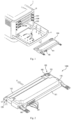
- FIG. 1-FIG. 4 show a structure of a developing cartridge used in the prior art.
- a developing cartridge 100 (100K, 100C, 100M, 100Y) is detachably installed into the main body 10 of a laser printer 1 along an installation direction A, where the developing cartridge 100 includes a cartridge body 110, a power reception unit 170 is provided on the end of one side of the cartridge body 110 close to a developing roller 140, a driving force reception unit 160 is provided on the end of the other side of the cartridge body 110 close to the developing roller 140, and a memory unit 180 is then provided on a back surface 101 of the cartridge body 110 of the developing cartridge 100 along the installation direction A of the developing cartridge 100, the memory unit is closer to the power reception unit 170 in relative to the driving force reception unit 160 and the memory unit 180 is provided with four terminals 181.
- the terminal contact point 13 on a cover 11 of the laser printer includes an end surface 131 and a side surface 132.
- the terminals 181 of the memory unit 180 come into contact with the front end surfaces 131 of the terminal contact points 13 on the cover 11.
- a circuit board 111 is provided inside the cover 11, and the electrical connections between the terminal contact points 13 on the cover 11 and the circuit board 111 are achieved via a spring 14.
- a press member 12 is provided on the cover 11 and is juxtaposed with the terminal contact point 13 at a certain distance, and when the cover 11 is closed, the press member 12 imposes a forward push force on the developing cartridge 100 installed in the main body 10, which may restrict the developing cartridge 100 from shifting forward and backward.
- the memory unit generally has two sides, where the front side is disposed with terminals that come into contact with the terminal contact points on the cover of the laser printer directly, and the reverse side is disposed with a memory as well as a capacitor, a resistor or other electronic components that are connected to the memory.
- the terminal contact points on the cover squeeze the memory to some degree to enable those electronic components welded onto the reverse side of the memory unit to become deformed or displaced due to the squeeze, thus the memory unit cannot work normally or even gets damaged, thereby affecting the developing cartridge to perform communications with the laser printer via the memory unit.
- the developing cartridges When a plurality of developing cartridges is installed into the main body of the laser printer together, there will be a certain gap between the developing cartridges.
- the developing cartridges usually enter and exit from the main body of the laser printer by the cooperation of a pair of or pairs of guide rail protrusions on two side plates of the developing cartridges with guide rails at two corresponding inner sides of the main body of the laser printer, and in order to easily install the developing cartridges into the printer and easily remove them from the printer, the guide rail protrusions on the developing cartridges must be in clearance fit with the guide rails inside the main body of the laser printer, in this case, when the laser printer starts to work, a driving force will cause the developing cartridges to vibrate up and down between guide clearances, this will bring about effects in two aspects: in one aspect, due to small contact areas between the terminals of the memory unit on back surfaces of the developing cartridges and the end surfaces of the terminal contact points on the cover, when the developing cartridges are vibrating up and down, elastic elongating and shortening
- Prior art document CN 202018562 U describes a chip with metal contacts.
- a laser printer with four processing boxes is disclosed, where each processing box includes a toner cartridge and a cover, and the toner cartridge includes the chip placement socket.
- the chip is disposed in the chip placement socket and one side of the chip has the metal contacts which are outward. When the cover of the laser printer is closed, the chip contacts of the cover are in contact with the metal contacts of the chip.
- Prior art document CN 102012667 A describes a chip fixing device and a processing box with the same for a laser printer, where the chip fixing device includes a base and a shield, and the base is provided with a slot and a support platform.
- the present invention provides a developing cartridge to solve the technical problem that an existing developing cartridge is prone to vibration up and down during its use and there will be a poor contact between terminals of memory unit and end surfaces of terminal contact points on a cover.
- the invention is set out in the appended set of claims.
- the conductive connecting pieces are provided on the upper surface (upper stepped surface) or the back surface (lower stepped surface) of the cartridge body, the side surfaces of the chip contact heads on the cover of the printer press the developing cartridge upward or downward when coming into contact with the conductive connecting pieces, which prevents the developing cartridge from vibrating up and down during use, thereby solving the technical problem that an existing developing cartridge may easily vibrate up and down during its use and there will be poor contacts between chip terminals and end surfaces of chip contact heads on a cover.
- the laser printer is the same as that in the background, and except the specially described structure of the developing cartridge, the remaining structures of the developing cartridge are the same as in the background.
- the present invention employs a technical solution of: achieving the limit of the developing cartridge in up and down directions by means of a squeezing contact formed between side surfaces of chip contact heads on the cover of the laser printer and an upper surface of a chip on a developing cartridge, and reference may be made to Embodiments 1, 2 and 3 for details. A brief description will be made hereunder on Embodiments 1, 2 and 3.
- the present invention uses conductive connecting pieces with larger areas to be securely connected to the chip terminals, the side surfaces of the chip contact heads on the cover of the laser printer then come into contact with the conductive connecting pieces with larger contact areas, and thus abnormal operation of the developing cartridge due to the poor contact may be reduced efficiently.
- a developing cartridge 500 (500K, 500Y) is installed into a main body of a laser printer
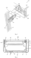
- chip contact heads 13 on the cover 11 after traveling a circular path R, come into contact with conductive connecting pieces 570 which are connected to a chip that is located on an upper stepped surface 502 of the developing cartridge 500, via side surfaces 132 of the chip contact heads.
- the side surfaces 132 of the chip contact heads 13 on the cover 11 contact, on one hand, with the conductive connecting pieces 570 connected to the chip, to achieve electrical connections, and on the other hand, press the conductive connecting pieces 570 to limit up and down vibrations of the developing cartridge 500; reference may be made to FIG. 6 for a pressed force F.
- the cover 11 has been designed with corresponding protrusions 12 which may press against the back 501 of the developing cartridge 500 when the cover 11 is closed, this may guarantee that the developing cartridge 500 will not vibrate in forward and backward directions.
- a developing cartridge 200 includes a cartridge body 30, and an upper surface of the cartridge body 30 is provided with a chip holder 36.
- Conductive connecting pieces 34 and a chip 35 are installed and fixed in the chip holder 36; limit posts 37 and receiving grooves 38 are successively provided on the upper surface 31 of the cartridge body 30 in compliance with rear ends of the conductive connecting pieces 34.
- the chip holder 36 includes: a plurality of supporting platforms 361 symmetrically provided at both ends of the chip holder 36, a plurality of limit blocks 362 provided at a side adjacent to the supporting platforms 361, baffles 363, and slots 364 formed between adjacent limit blocks 362; the receiving grooves 38 locate at a rear end of the chip holder 36, and limit posts 37 locate between the chip holder 36 and the receiving grooves 38.
- the conductive connecting piece 34 includes: a rear end 346, a central I-shaped hole 343, a front-end bend portion 344 and barbed teeth 345 thereon; the conductive connecting piece further includes: a protrusion 342 in contact with the chip terminal, where the protrusion 342 is formed by stamping in a direction where the conductive connecting piece 34 extends towards the front-end bend portion 344.
- FIG. 10 is a schematic diagram where the conductive connecting pieces 34 come into contact with the side surfaces 132 of the chip contact heads 13 of the laser printer when being connected to the chip 35.
- FIG. 7, FIG. 8 , FIG. 9A, FIG. 9B and FIG. 10 when the terminals 351 of the chip 35 is placed facing up on the supporting platforms 361 in the chip holder 36, the limit blocks 362 in the front of the chip holder 36 and the baffles at three sides of the rear play a role of limiting the chip 35 on all sides, then the conductive connecting pieces 34 are placed across the chip 35 successively so that the front-end bend portions 344 of the conductive connecting pieces 34 are reversely inserted into the slots 334 in the front of the chip holder 36 successively, and since edges of the front-end bend portions 344 of the conductive connecting pieces 34 are carried with the barbed teeth 345, it is difficult for the front-ends of the conductive connecting pieces 34 to loose and out from the slots 364; meanwhile the protrusions 342 formed by stamping on the conductive connecting pieces 34 are abutting joint with the chip terminals 351 one by one, the I-shaped holes 343 in the middle of the conductive connecting
- the following structural changes may also be made to the chip holder, the limit posts and the receiving grooves of the conductive connecting pieces.
- a chip holder 36' includes: a plurality of supporting platforms 361', limit blocks 362', baffles 363' and slots 365', symmetrically provided at both ends of the chip holder 36'.
- a chip 35' includes: terminals 351' on the front side, notches 352' and protrusions 353' at left and right ends.
- a conductive connecting piece 34' includes: a front-end bending protrusion 341', a central hole 343' and a rear-end contact part 346'.
- FIG. 11-FIG. 15 when the terminals 351' on a front side of the chip 35' are placed facing up on the chip supporting platforms 361' in the chip holder 36', two limit blocks 362' in the front of the chip holder 36' are just caught in the chip notches 352', the baffles 363' at three sides of the rear play a role of limiting the chip 35' on all sides, and meanwhile the protrusions 353' at left and right ends of the chip fit in with the slots 365' in the chip holder 36', then the rear-end contact parts 346' of the conductive connecting pieces 34' are placed in receiving grooves 38', and then the central holes 343' of the conductive connecting pieces 34' are pressed and socketed to the limit posts 37' in turn, at this time, the front-end bending protrusions 341' of the conductive connecting pieces 34' are abutting joint with the terminals 351' of the chip one by one, and press the chip 35'downward
- a push bar 33' may be provided at the ends of the receiving grooves 38' of the conductive connecting pieces.
- FIG. 15 when the side surfaces 132 of the chip contact heads 13 of the printer come into contact with the rear-end contact parts 346' of the conductive connecting pieces 34', the end surfaces 131 of the chip contact heads 13 of the printer will press against the push bar 33'.
- the push bar 33' will impose a backward push force on the chip contact heads 13 of the laser printer to ensure good connections among a circuit board 111, springs 14 and the chip contact heads 13 inside the cover 11.
- a developing cartridge 300 includes a cartridge body 40, and a stepped surface 41 is provided at the back end of the upper surface of the cartridge body 40, where the stepped surface 41 is provided with a chip holder 43, setting the stepped surface may prevent components on the chip holder and elements mounted thereon from being scraped during the process of installing and disassembling the developing cartridge.
- Conductive connecting pieces 44 and a chip 45 are installed and fixed on the chip holder 43, and the chip holder 43 includes one pair of supporting platforms 46, two rows of limit posts 47, elastic fixing buckles 48 and elastic limit buckles 49.
- FIG. 17 For position relations of the components on the chip holder 43, reference may be made to a locally exploded view of the developing cartridge as shown in FIG. 17 and a structural diagram of the chip holder 43 as shown in FIG. 18 , where the two rows of limit posts 47 mainly function as limiting and fixing the conductive connecting pieces 44, which are provided at a position close to the front of the chip holder 43; the elastic fixing buckles 48 and the elastic limit buckles 49 are provided at both ends of the chip holder 43 respectively; the one pair of supporting platforms 46 mainly function as supporting and limiting the chip 45, and the elastic fixing buckles 48 and the elastic limit buckles 49, which correspond to the one pair of supporting platforms, is provided at a position away from the chip holder 43.
- the chip 45 includes: terminals 451 on the front side of the chip, stepped ends 452 at both ends of the reverse side of the chip and a notch 453.
- the conductive connecting piece 44 includes: a front-end limit hole 442, a central protrusion 441 and a back-end arch-shaped contact surface 443.
- FIG. 21 is a view of the conductive connecting pieces 44 coming into contact with side surfaces of the chip contact heads 13 of the laser printer when being connected to the chip 45.
- the central protrusions 441 and the back-end arch-shaped contact surfaces 443 of the conductive connecting pieces 44 are placed facing up to enable the limit holes 442 on the conductive connecting pieces to face the limit posts 47 of the chip holder 43 and be socketed thereto, the limit posts 47 and the limit holes 442 are in a state of interference fit herein so as to restrict the conductive connecting pieces 44 from moving, then the terminals 451 on the front side of the chip 45 is placed facing down on the supporting platforms 46, the supporting platforms 46 not only may support the chip 45, but also restrict the chip 45 from moving forward and backward, and at this time, the terminals 451 of the chip just come into contact with the protrusions 441 on the conductive connecting pieces 44, meanwhile the stepped end 452 at one end of the reverse side of the chip 45 is inserted into the elastic fixing buckles 48, the stepped end 452 at the other end of the reverse side of the chip 45 is pressed into the elastic limit buckles 49, and thus
- the assembly process where the conductive connecting pieces 44 come into contact with the chip 45 is finished.
- the cover 11 of the laser printer is closed, the end surfaces 131 of the chip contact heads 13 of the printer come into contact with the arch-shaped contact surfaces 443 of the conductive connecting pieces firstly, and then slide towards the front ends of the conductive connecting pieces 44 till the side surfaces 132 of the chip contact heads 13 of the printer and the arch-shaped contact surfaces 443 achieve pressure contacts. Then, electrical connections are achieved among the chip 45, the conductive connecting pieces 44 and the chip contact heads 13 of the printer.
- a developing cartridge 400 includes a cartridge body 70, where the cartridge body 70 includes an upper stepped surface 71 and a back surface 91.
- the back surface 91 of the cartridge body 70 is provided with a chip holder 73.
- a chip 75 is provided with chip terminals 751 and a notch 752;
- conductive connecting pieces 74 are provided with circular I-shaped holes 741 and back-end contact surfaces 742;
- the upper stepped surface 71 of the cartridge body 70 is provided with a plurality of limit posts 77 matching the number of the chip terminals and a plurality of elastic limit buckles 79 arranged in a row.
- the chip 75 and the conductive connecting pieces 74 are connected via springs 76, the springs 76 are provided in spring holes 78 which run through the upper stepped surface 71 and the back surface 91 of the cartridge body 70; one end of the spring 76 stands against the terminal 751, and the other end of the spring stands against the conductive connecting piece 74.
- the chip holder 73 is further provided with a screw hole 81, and the chip 75 is fixed in the chip holder 73 via a screw 80.
- the developing cartridge is omitted, as shown in FIG. 25 .
- FIG. 22-FIG. 25 firstly, on the back surface 91 of the cartridge body 70, the terminals 751 on the front side of the chip 75 are placed in the chip holder 73 into which the spring holes 78 are provided, and the screw 80 is used to secure the chip 75 after the notch 752 of the chip is aligned with the screw hole 81.
- the springs 76 are placed in the corresponding spring holes 78 respectively, and then the circular I-shaped holes 741 of the conductive connecting pieces 74 are pressed and socketed to the limit posts 77, meanwhile the back-end contact surfaces 742 of the conductive connecting pieces 74 are pressed into the elastic limit buckles 79, in this case, one end of the spring 76 stands against the terminal 751 of the chip, the other end of the spring stands against the back-end contact surface 742 of the conductive connecting piece 74, and then electrical connections between the conductive connecting pieces 74 and the chip 75 are achieved. Then, the assembly process where the conductive connecting pieces 74 come into contact with the chip 75 via the springs 76 is achieved.
- the conductive connecting pieces have a structure as shown in FIG. 31 .
- the conductive connecting piece 64 includes: a front-end limit hole 642, an elastic sheet 641 stamped in the middle and a back-end arch-shaped contact surface 643.
- the front-end limit hole 642 is engaged with the limit post 77, the elastic sheet 641 stands against the terminal 751 of the chip, and then electrical connections between the conductive connecting pieces 64 and the chip 75 are achieved.
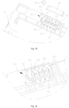
- the limit posts in this embodiment may also have a replaced structure as follows. As shown in FIG. 26-FIG. 30 , at a position corresponding to a chip holder 63 of a back surface 51 of a cartridge body 60, a press bar 67 is provided on an upper stepped surface 61 of the cartridge body 60, where the press bar 67 is located at front ends of the conductive connecting pieces 64; a plurality of limit posts 671 matching the number of the terminals of the chip is provided at the back (that is, facing towards the back surface 51 of the cartridge body 60) of the press bar 67, the front ends of the conductive connecting pieces 64 are inserted into the back of the press bar 67 to enable the limit holes 642 on the conductive connecting pieces 64 to be pressed and socketed to the limit posts 671 of the press bar 67 in turn, here, the limit posts 671 may be hot melted so as to better secure the conductive connecting pieces 64.
- the structure of the chip may be replaced by the structure of the chip 45 as shown in FIG. 19 , and the chip holder may be provided with a chip supporting platform, as shown in FIG. 27 , FIG. 29 and FIG. 30 , a chip supporting platform 62 is provided at the right side of the chip holder 63, which together with a screw 50 support and fix the chip 45.
- a push bar is provided, as shown in FIG. 26 , FIG. 28 and FIG. 32 , a push bar 66 parallel to the press bar 67 is provided close to the back end, and the push bar 66 will impose a backward push force on the end surfaces of the chip contact heads 13 of the laser printer to ensure good connections among a circuit board 111, springs 14 and the chip contact heads 13 inside the cover 11.
- FIG. 26-FIG. 32 firstly, on the upper stepped surface 61 of the cartridge body 60 of a developing cartridge 600, the conductive connecting pieces 64 are successively inserted along slots 661 that are below the push bar 66 so that the elastic sheets 641 which are formed by stamping the middle of the conductive connecting pieces 64 enter into through holes 68 below limit buckles 69 and back ends of the conductive connecting pieces 64 extend to the below of the press bar 67.
- the limit posts 671 may be hot melted so as to better secure the conductive connecting pieces 64, then the terminals 451 on the front side of the chip 45 face the through holes 68 so that the stepped end 452 at one end of the chip 45 is inserted into the chip supporting platform 62 of the chip holder 63 and the stepped end 452 at the other end is pressed into the chip holder 63 correspondingly, at this time, the terminals 451 on the chip 45 come into contact with the elastic sheets 641 on the conductive connecting pieces 64 which pass through the through holes 68, one by one accordingly, and the chip 45 is just caught between baffles 58 of the chip holder 63 and limit blocks 59 of the chip holder 63 in a length direction of the chip, meanwhile the notch 453 on the chip 45 stands against a catching block
- a handle 630 is provided at a position close to the middle of the back end of the cartridge body 60, as shown in FIG. 26 .
- Setting the handle 630 may guarantee the convenience of installing the developing cartridge into the main body of the printer or disassembling it from the main body of the printer.
- Embodiment 3 the same structural features as in Embodiment 3 will not be repeated here; while the difference lies in the manner in which the back ends of the conductive connecting pieces are brought into contact with side surfaces of the chip contact heads on the cover of the printer.
- a conductive connecting piece 64' includes: a front-end limit hole 642', an elastic sheet 641' stamped in the middle, and a contact surface 643' and a guide surface 644' that bend upward and extend from both sides of the back end respectively, where functions and assembly and contact modes of parts of the conductive connecting piece 64' are the same as those of the conductive connecting piece 64, except the contact surface 643' and the guide surface 644' that bend upward and extend from both sides of the back end of the conductive connecting piece 64', the guide surface 644' extending from an end of the contact surface 643' in a certain degree.
- the chip contact head 13 on the cover of the printer is guided by two guide surfaces 644' at the back end of the conductive connecting piece 64' to enter between two contact surfaces 643', and since the two guide surfaces 644' open towards two sides, they may succeed in guiding the chip contact head 13 along the two contact surfaces 643', and the two contact surfaces 643' squeeze side surface of the chip contact head 13 to some extent and catch the chip contact head 13 between the two contact surface 643', a close-fitted engagements may be achieved between the chip contact head 13 on the cover of the printer and the conductive connecting piece 64', meanwhile a plurality of separators 661 extending from the push bar 66 may prevent the guide surfaces 644' at the back ends of adjacent conductive connecting pieces 64' from contacting with each other.
- a bottom contact surface may be formed by extending between the contact surfaces bending upward and extending from both sides of the back end of the conductive connecting piece, along bottom surface of the back end of the conductive connecting piece.
- a developing cartridge 700 includes a cartridge body 800, where an upper surface 803 of the cartridge body 800 is provided with a chip assembly 810, and a back surface 801 of the cartridge body 800 is provided with a conductive connecting piece assembly 820 at a position corresponding to the chip assembly 810.
- the chip assembly 810 includes a chip 850 and a chip holder 811, the chip holder 811 is provided with a chip slot 812, a protrusion 813 and a reserved space 814.
- the conductive connecting piece assembly 820 includes a conductive connecting piece 840 and a holder 821 thereof, the holder 821 is provided with a conductive connecting piece slot 822 and an adhesive locating post 823.
- the chip 850 includes a substrate 854, terminals 851 disposed on a front side 855 (as shown in FIG. 41A ) of the substrate 854 and electronic components 852 disposed on a reverse side 856 (as shown in FIG. 41B ) of the substrate 854. There is an open slot 853 on the substrate 854.
- the conductive connecting piece 840 includes a printer contact part 841 (in contact with the chip contact head 13 on the cover 11 of the laser printer), where the printer contact parts 841 is provided with teeth 842 in the shape of a right angled triangle; the conductive connecting piece 840 also includes a transition area 844 and an elastic contact part 843 (in elastic contact with the terminals 851 of the chip 850), where a plane in which the transition areas 844 is located is perpendicular to a plane in which the printer contact part 841 is located, the elastic contact part 843 is the front part of the transition area 844 and the elastic contact part 843 is an elastic surface bending inwards slightly.
- the printer contact part 841 together with the teeth 842 thereon enter into the conductive connecting piece slot 822, and at this time, the adhesive locating post 823 on the holder 821 of the conductive connecting pieces is just brought into contact with and adhere to the transition area 844 of the conductive connecting piece 840.
- the elastic contact part 843 on the conductive connecting piece 840 is in elastic contact with the terminals 851 on the chip 850 correspondingly.
- the above chip holder and the holder of the conductive connecting piece may be provided on the cartridge body of the developing cartridge separately, and may also be integrally injection-molded with the cartridge body of the developing cartridge. Moreover, corresponding to the position of the upper surface 803 of the cartridge body 800, the chip assembly 810 may also be provided on a back surface 802 of the cartridge body 800, and then the conductive connecting piece assembly 820 is provided on the upper surface 803 of the cartridge body 800 in compliance with the chip assembly 810.
- Communication function between the developing cartridge and the laser printer via the chip can be achieved according to Embodiment 5, and direct contacts between the terminals of the chip and the chip contact heads on the cover of the laser printer are avoided, which will cause those electronic components welded onto the reverse side of the chip to become deformed or misplaced due to the squeeze, thereby solving the problem of chip malfunctioning and even being damaged, which is the problem intended to be solved in the background technology.
- Embodiments 1, 2 and 3 are based on the optimal and most convenient design solutions without departing from the keystone that the developing cartridge comes into contact with the side surfaces of the chip contact heads of the printer via the conductive connecting pieces on the upper surface or the upper stepped surface of the cartridge body, and structures of the chip holder, the conductive connecting pieces and the chip as described in embodiments of the present invention above may be freely combined according to specific designs.
- the developing cartridge which has been installed with the chip, the conductive connecting pieces and other components described in Embodiments 1, 2 and 3 above is loaded into the main body of the laser printer, as shown in FIG. 5-FIG. 6, where during the process of closing the cover 11, the chip contact heads 13 on the cover 11, after traveling a circular path R, come into contact, via the side surfaces 132, with the conductive connecting pieces 570 which are connected to the chip and located on the upper stepped surface 502 of the developing cartridge 500, and press the developing cartridge 500 downward.
- the side surfaces 132 of the chip contact heads 13 on the cover 11 contact, on one hand, with the conductive connecting pieces 570 connected to the chip, to achieve electrical connections, and on the other hand, press the conductive connecting pieces 570 to limit up and down vibrations of the developing cartridge 500 between guide gaps; reference may be made to FIG. 6 for a pressed force F.
- the cover 11 has been designed with corresponding protrusions 12 which may press against the back 501 of the developing cartridge 500 when the cover 11 is closed, this may guarantee that the developing cartridge 500 will not vibrate in front and back directions.
- the number of the conductive connecting pieces is determined according to the number of the memory terminals.
- a conductive elastic material may be adhered at the back ends where the conductive connecting pieces come into contact with the side surfaces of the chip contact heads on the cover of the printer; such material has adhesiveness at the sides that are in contact with the back ends of the conductive connecting pieces, and such material has electrical-conductivity as a whole and elasticity; when the side surfaces of the chip contact heads on the cover come into contact with and press such conductive elastic material, such conductive elastic material may be deformed rapidly and cover the side surfaces of the chip contact heads to achieve flexible electrical connections between the side surfaces of the chip contact heads and the conductive connecting pieces, and in this case, contact areas of the side surfaces of the chip contact heads will become larger and more efficient, which further ensures good contacts between the side surfaces of the chip contact heads and the conductive connecting pieces, such conductive elastic material may be, for example,
- conductive connecting piece 64" includes: a front-end limit hole 642", an elastic sheet 641” stamped in the middle and a back-end contact surface 643", where functions and assembly and contact modes of parts of the conductive connecting pieces 64" are the same as those of the conductive connecting piece 64, the difference therebetween lies in that the back-end contact surface 643" of the conductive connecting piece 64" is adhered with a conductive elastic sponge 56.
- FIG. 36 shows a view where the side surfaces of the chip contact heads 13 on the cover of the laser printer come into contact with the conductive connecting pieces 64" adhered with the conductive elastic sponge 56 at the back ends thereof, where a plurality of conductive elastic sponges 56 are separated by a plurality of separators 661 extending from the push bar 66.
- the separator 611 may prevent the plurality of conductive elastic sponges 56 from contacting with each other.
- FIG. 37 shows a schematic diagram where the side surfaces 132 of the chip contact heads 13 on the cover of the laser printer come into contact with terminals 581 on the front surface of the chip 580.
- contacts between the memory terminals on the developing cartridge and the side surfaces of the chip contact heads on the cover can be achieved according to technical solutions in Embodiments 1, 2 and 3, and reliability of the contacts increases, moreover, the developing cartridge has decreased vibration during a printing process, avoiding effects on the developing process, and ensuring stability of printing quality, thereby solving the problem of poor contacts between the chip terminals on the developing cartridge and the end surfaces of the chip contact heads on the cover, which is what is intended to be solved in the background, and meanwhile additionally solving the technical problem of shifting of a developing roller and a photosensitive drum due to vibrations and thus affecting the developing process and causing the printing quality unstable.
Landscapes
- Physics & Mathematics (AREA)
- General Physics & Mathematics (AREA)
- Engineering & Computer Science (AREA)
- Computer Vision & Pattern Recognition (AREA)
- Electrophotography Configuration And Component (AREA)
Claims (5)
- Entwicklungskartusche (500, 600), die abnehmbar in einem Drucker installiert ist, wobei eine Abdeckung (11) des Druckers mit einer Vielzahl von Chipkontaktköpfen (13) versehen ist, wobei jeder der Chipkontaktköpfe (13) eine Endfläche (131) und eine Seitenfläche (132) umfasst, wobei die Entwicklungskartusche (500, 600) umfasst:einen Kartuschenkörper (60) und einen Chip (45, 75) und eine Vielzahl von leitenden Verbindungsstücken (64), die auf dem Kartuschenkörper (60) vorgesehen sind, wobei der Kartuschenkörper (60) eine obere Fläche, die nach oben gerichtet ist, und eine hintere Fläche (51) aufweist, die nach unten gerichtet ist, wenn die Entwicklungskartusche (500, 600) installiert und in den Drucker eingesetzt ist,dadurch gekennzeichnet, dass ein Ende jedes leitenden Verbindungsstücks (64) mit einem Chipanschluss (451, 751) verbunden ist, und dass, wenn die Entwicklungskartusche (500, 600) installiert und in den Drucker eingesetzt ist und die Abdeckung (11) geschlossen ist, das andere Ende des leitenden Verbindungsstücks (64) mit der Seitenfläche (132) eines entsprechenden Chipkontaktkopfes (13) auf der Abdeckung (11) des Druckers in Kontakt kommt, so dass die Seitenflächen (132) der Chipkontaktköpfe (13) auf der Abdeckung (11) des Druckers die Entwicklungskartusche (500, 600) nach oben oder unten drücken, wenn sie in Kontakt mit den leitenden Verbindungsstücken (64) kommen, und ein Leseende der oberen Fläche des Kartuschenkörpers (60) mit einer abgestuften Fläche (61, 502) versehen ist, wobei das Leseende nahe an der Vielzahl von Chipkontaktköpfen (13) auf der Abdeckung (11) liegt, und die Vielzahl von leitenden Verbindungsstücken (64) auf der abgestuften Fläche (61, 502) vorgesehen sind,wobei die Entwicklungskartusche (500, 600) ferner einen Chiphalter (63, 73) umfasst, wobei der Chiphalter (63, 73) auf der Rückseite (51) des Kartuschenkörpers (60) vorgesehen ist und der Chip (45, 75) in dem Chiphalter (63, 73) installiert und befestigt ist,wobei jedes der leitenden Verbindungsstücke (64) umfasst: ein vorderseitiges Begrenzungsloch (642), ein in der Mitte gestanztes elastisches Blatt (641) und eine rückseitige bogenförmige Kontaktfläche (643); wobei an einer Position, die dem Chiphalter (63) entspricht, die obere abgestufte Fläche (61) des Kartuschenkörpers (60) mit einem Pressbalken (67) versehen ist, und Begrenzungsschnallen (69), die in einer Reihe angeordnet sind, ein Durchgangsloch (68), das durch die obere abgestufte Fläche (61) und die hintere Fläche (51) des Kartuschenkörpers (60) verläuft, vorgesehen ist, der Pressbalken (67) am vorderen Ende jedes der leitenden Verbindungsstücke (64) angeordnet ist, eine Vielzahl von Begrenzungspfosten (671), die der Anzahl der Chipanschlüsse (451) entsprechen, an der Rückseite des Pressbalkens (67) vorgesehen sind, das vordere Ende jedes der leitenden Verbindungsstücke (64) in die Rückseite des Pressbalkens (67) eingeführt ist, die Begrenzungslöcher (642) der leitenden Verbindungsstücke (64) nacheinander in die Begrenzungspfosten (671) des Pressbalkens (67) gepresst und eingesteckt werden die Begrenzungspfosten (671) und die leitenden Verbindungsstücke (64) in einer Heißschmelzbefestigungsverbindung stehen, die elastischen Blätter (641) durch die Durchgangslöcher (68) hindurchgehen, um gegen die Chipanschlüsse (451) zu stehen, um elektrische Verbindungen zwischen den leitenden Verbindungsstücken (64) und dem Chip (45) zu erreichen.
- Entwicklungskartusche (500, 600) nach Anspruch 1, wobei die Mehrzahl von leitenden Verbindungsstücken (64) auf der oberen Oberfläche des Kartuschenkörpers (60) vorgesehen ist.
- Entwicklungskartusche (500, 600) nach Anspruch 1, wobei ein Schraubenloch (52), das durch die obere abgestufte Fläche (61) und die hintere Fläche (51) des Kartuschenkörpers (60) verläuft, vorgesehen ist.
- Entwicklungskartusche (500, 600) nach Anspruch 3, wobei der Chip (45) ferner umfasst: abgestufte Enden (452), die an beiden Enden der Rückseite des Chipanschlusses (451) vorgesehen sind, und der Chiphalter (63) ferner eine Stützplattform (62) umfasst, wobei das abgestufte Ende (452) an einem Ende des Chips (45) in die Stützplattform (62) eingesetzt ist und das abgestufte Ende (452) an dem anderen Ende in dem Chiphalter (63) durch eine Schraube (50), die durch das Schraubenloch (52) hindurchgeht, befestigt ist.
- Die Entwicklungskartusche (500, 600) nach einem der Ansprüche 1 bis 4, ferner eine Druckstange (66) umfassend, die in der Lage ist, gegen die Endflächen der Chipkontaktköpfe (13) des Druckers zu stehen und eine Rückwärtsdruckkraft auf die Chipkontaktköpfe (13) des Druckers auszuüben.
Applications Claiming Priority (4)
| Application Number | Priority Date | Filing Date | Title |
|---|---|---|---|
| CN201320838368.6U CN203673222U (zh) | 2013-12-18 | 2013-12-18 | 一种显影盒 |
| CN201420479297 | 2014-08-22 | ||
| CN201410608971.4A CN105629691B (zh) | 2014-08-22 | 2014-10-31 | 一种显影盒 |
| PCT/CN2014/092900 WO2015090142A1 (zh) | 2013-12-18 | 2014-12-03 | 一种显影盒 |
Publications (4)
| Publication Number | Publication Date |
|---|---|
| EP3086181A1 EP3086181A1 (de) | 2016-10-26 |
| EP3086181A4 EP3086181A4 (de) | 2017-10-18 |
| EP3086181B1 true EP3086181B1 (de) | 2025-02-19 |
| EP3086181C0 EP3086181C0 (de) | 2025-02-19 |
Family
ID=56936216
Family Applications (1)
| Application Number | Title | Priority Date | Filing Date |
|---|---|---|---|
| EP14870774.8A Active EP3086181B1 (de) | 2013-12-18 | 2014-12-03 | Entwicklungsbox |
Country Status (2)
| Country | Link |
|---|---|
| US (1) | US9785110B2 (de) |
| EP (1) | EP3086181B1 (de) |
Families Citing this family (10)
| Publication number | Priority date | Publication date | Assignee | Title |
|---|---|---|---|---|
| JP6590534B2 (ja) | 2015-05-29 | 2019-10-16 | キヤノン株式会社 | プロセスカートリッジ及び画像形成装置 |
| JP6566806B2 (ja) * | 2015-09-16 | 2019-08-28 | キヤノン株式会社 | カートリッジおよび軸受部材 |
| US9996052B2 (en) * | 2016-02-10 | 2018-06-12 | Canon Kabushiki Kaisha | Cartridge capable of being inserted in an apparatus main body of an image forming apparatus |
| JP6880925B2 (ja) * | 2017-03-30 | 2021-06-02 | ブラザー工業株式会社 | 現像カートリッジ |
| JP6809337B2 (ja) * | 2017-03-30 | 2021-01-06 | ブラザー工業株式会社 | 現像カートリッジ |
| JP6992720B2 (ja) * | 2018-09-27 | 2022-01-13 | 沖電気工業株式会社 | 画像形成装置 |
| US11409225B2 (en) * | 2019-12-27 | 2022-08-09 | Canon Kabushiki Kaisha | Image forming apparatus with draw-out unit having electrically contactable contact pairs |
| US11392078B2 (en) | 2020-04-24 | 2022-07-19 | Lexmark International, Inc. | Electrical connector assembly for an image forming device |
| DE212021000253U1 (de) * | 2020-08-10 | 2022-08-31 | Jiangxi Yibo E-Tech Co., Ltd. | Entwicklungskartusche, Trommelkartusche und Bilderzeugungsvorrichtung |
| CN115755551A (zh) * | 2022-11-14 | 2023-03-07 | 珠海奔图电子有限公司 | 一种导电连接结构及图像形成装置 |
Citations (3)
| Publication number | Priority date | Publication date | Assignee | Title |
|---|---|---|---|---|
| US20030123896A1 (en) * | 2001-12-28 | 2003-07-03 | Canon Kabushiki Kaisha | Process cartridge and electrophotographic image forming apparatus |
| WO2010018816A1 (ja) * | 2008-08-12 | 2010-02-18 | パナソニック電工株式会社 | メモリカードソケット |
| CN202018562U (zh) * | 2011-04-13 | 2011-10-26 | 珠海赛纳打印科技股份有限公司 | 一种处理盒 |
Family Cites Families (4)
| Publication number | Priority date | Publication date | Assignee | Title |
|---|---|---|---|---|
| JP3600391B2 (ja) | 1997-01-07 | 2004-12-15 | 株式会社リコー | 画像形成装置 |
| CN102012667B (zh) | 2010-11-04 | 2012-07-04 | 珠海天威飞马打印耗材有限公司 | 芯片固定装置及带有该装置的激光打印机用处理盒 |
| KR101833375B1 (ko) * | 2011-07-21 | 2018-02-28 | 에스프린팅솔루션 주식회사 | 현상카트리지 및 이를 포함하는 화상형성장치 |
| CN202975595U (zh) | 2012-11-29 | 2013-06-05 | 珠海天威飞马打印耗材有限公司 | 碳粉盒 |
-
2014
- 2014-12-03 EP EP14870774.8A patent/EP3086181B1/de active Active
-
2016
- 2016-06-14 US US15/181,977 patent/US9785110B2/en active Active
Patent Citations (3)
| Publication number | Priority date | Publication date | Assignee | Title |
|---|---|---|---|---|
| US20030123896A1 (en) * | 2001-12-28 | 2003-07-03 | Canon Kabushiki Kaisha | Process cartridge and electrophotographic image forming apparatus |
| WO2010018816A1 (ja) * | 2008-08-12 | 2010-02-18 | パナソニック電工株式会社 | メモリカードソケット |
| CN202018562U (zh) * | 2011-04-13 | 2011-10-26 | 珠海赛纳打印科技股份有限公司 | 一种处理盒 |
Also Published As
| Publication number | Publication date |
|---|---|
| US9785110B2 (en) | 2017-10-10 |
| EP3086181A1 (de) | 2016-10-26 |
| EP3086181C0 (de) | 2025-02-19 |
| US20160349697A1 (en) | 2016-12-01 |
| EP3086181A4 (de) | 2017-10-18 |
Similar Documents
| Publication | Publication Date | Title |
|---|---|---|
| EP3086181B1 (de) | Entwicklungsbox | |
| JP5013278B2 (ja) | Icカード用コネクタ | |
| US9823714B2 (en) | Hard disk quick release unit and hard disk replacement module | |
| RU2013107402A (ru) | Картридж для печатающего материала и система подачи печатающего материала | |
| JP2012221592A (ja) | コネクタ | |
| CN105629691A (zh) | 一种显影盒 | |
| WO2012118478A1 (en) | A spring loaded lid | |
| CN112421321A (zh) | 卡座装置和电子设备 | |
| EP2937944A1 (de) | Steckverbinder | |
| JP2020508246A (ja) | チップ、インクカートリッジおよびインクカートリッジ取り出し方法 | |
| JP2014006955A (ja) | ハードディスク固定装置 | |
| JP4403458B2 (ja) | チップトレイ | |
| JP2003115354A (ja) | カード用コネクタ | |
| CN115275680A (zh) | 卡座组件及电子设备 | |
| CN217372015U (zh) | 一种处理盒芯片拆装夹具 | |
| WO2015090142A1 (zh) | 一种显影盒 | |
| CN112886297B (zh) | 堆叠式卡座 | |
| US8098444B2 (en) | Clutching jig | |
| JP2009016042A (ja) | メモリカード用ソケット | |
| CN203405672U (zh) | 一种存储元件容纳单元及显影盒 | |
| CN205193433U (zh) | 一种显影盒 | |
| CN117944371A (zh) | 芯片及墨盒 | |
| KR102099704B1 (ko) | 배터리 커넥터 | |
| JP7160558B2 (ja) | 車載装置 | |
| CN214427751U (zh) | 一种显影盒 |
Legal Events
| Date | Code | Title | Description |
|---|---|---|---|
| PUAI | Public reference made under article 153(3) epc to a published international application that has entered the european phase |
Free format text: ORIGINAL CODE: 0009012 |
|
| 17P | Request for examination filed |
Effective date: 20160714 |
|
| AK | Designated contracting states |
Kind code of ref document: A1 Designated state(s): AL AT BE BG CH CY CZ DE DK EE ES FI FR GB GR HR HU IE IS IT LI LT LU LV MC MK MT NL NO PL PT RO RS SE SI SK SM TR |
|
| AX | Request for extension of the european patent |
Extension state: BA ME |
|
| DAX | Request for extension of the european patent (deleted) | ||
| RIN1 | Information on inventor provided before grant (corrected) |
Inventor name: WANG, PENG Inventor name: LUO, LAI Inventor name: YIN, ZHONGLI Inventor name: LIN, HUASHEN Inventor name: HUANG, WANHONG Inventor name: WANG, CHAO Inventor name: CAO, JIANXIN Inventor name: WEI, SHENGYU |
|
| RIC1 | Information provided on ipc code assigned before grant |
Ipc: G03G 21/18 20060101ALI20170906BHEP Ipc: G03G 15/08 20060101AFI20170906BHEP |
|
| A4 | Supplementary search report drawn up and despatched |
Effective date: 20170914 |
|
| RAP1 | Party data changed (applicant data changed or rights of an application transferred) |
Owner name: NINESTAR CORPORATION |
|
| STAA | Information on the status of an ep patent application or granted ep patent |
Free format text: STATUS: EXAMINATION IS IN PROGRESS |
|
| 17Q | First examination report despatched |
Effective date: 20210507 |
|
| GRAP | Despatch of communication of intention to grant a patent |
Free format text: ORIGINAL CODE: EPIDOSNIGR1 |
|
| STAA | Information on the status of an ep patent application or granted ep patent |
Free format text: STATUS: GRANT OF PATENT IS INTENDED |
|
| RIC1 | Information provided on ipc code assigned before grant |
Ipc: G03G 21/16 20060101ALI20241002BHEP Ipc: G03G 21/18 20060101ALI20241002BHEP Ipc: G03G 15/08 20060101AFI20241002BHEP |
|
| INTG | Intention to grant announced |
Effective date: 20241017 |
|
| GRAS | Grant fee paid |
Free format text: ORIGINAL CODE: EPIDOSNIGR3 |
|
| GRAA | (expected) grant |
Free format text: ORIGINAL CODE: 0009210 |
|
| STAA | Information on the status of an ep patent application or granted ep patent |
Free format text: STATUS: THE PATENT HAS BEEN GRANTED |
|
| AK | Designated contracting states |
Kind code of ref document: B1 Designated state(s): AL AT BE BG CH CY CZ DE DK EE ES FI FR GB GR HR HU IE IS IT LI LT LU LV MC MK MT NL NO PL PT RO RS SE SI SK SM TR |
|
| REG | Reference to a national code |
Ref country code: GB Ref legal event code: FG4D |
|
| REG | Reference to a national code |
Ref country code: CH Ref legal event code: EP |
|
| REG | Reference to a national code |
Ref country code: IE Ref legal event code: FG4D |
|
| REG | Reference to a national code |
Ref country code: DE Ref legal event code: R096 Ref document number: 602014091583 Country of ref document: DE |
|
| U01 | Request for unitary effect filed |
Effective date: 20250313 |
|
| U07 | Unitary effect registered |
Designated state(s): AT BE BG DE DK EE FI FR IT LT LU LV MT NL PT RO SE SI Effective date: 20250319 |
|
| PG25 | Lapsed in a contracting state [announced via postgrant information from national office to epo] |
Ref country code: RS Free format text: LAPSE BECAUSE OF FAILURE TO SUBMIT A TRANSLATION OF THE DESCRIPTION OR TO PAY THE FEE WITHIN THE PRESCRIBED TIME-LIMIT Effective date: 20250519 |
|
| PG25 | Lapsed in a contracting state [announced via postgrant information from national office to epo] |
Ref country code: PL Free format text: LAPSE BECAUSE OF FAILURE TO SUBMIT A TRANSLATION OF THE DESCRIPTION OR TO PAY THE FEE WITHIN THE PRESCRIBED TIME-LIMIT Effective date: 20250219 |
|
| PG25 | Lapsed in a contracting state [announced via postgrant information from national office to epo] |
Ref country code: ES Free format text: LAPSE BECAUSE OF FAILURE TO SUBMIT A TRANSLATION OF THE DESCRIPTION OR TO PAY THE FEE WITHIN THE PRESCRIBED TIME-LIMIT Effective date: 20250219 |
|
| PG25 | Lapsed in a contracting state [announced via postgrant information from national office to epo] |
Ref country code: IS Free format text: LAPSE BECAUSE OF FAILURE TO SUBMIT A TRANSLATION OF THE DESCRIPTION OR TO PAY THE FEE WITHIN THE PRESCRIBED TIME-LIMIT Effective date: 20250619 Ref country code: NO Free format text: LAPSE BECAUSE OF FAILURE TO SUBMIT A TRANSLATION OF THE DESCRIPTION OR TO PAY THE FEE WITHIN THE PRESCRIBED TIME-LIMIT Effective date: 20250519 |
|
| PG25 | Lapsed in a contracting state [announced via postgrant information from national office to epo] |
Ref country code: HR Free format text: LAPSE BECAUSE OF FAILURE TO SUBMIT A TRANSLATION OF THE DESCRIPTION OR TO PAY THE FEE WITHIN THE PRESCRIBED TIME-LIMIT Effective date: 20250219 |
|
| PG25 | Lapsed in a contracting state [announced via postgrant information from national office to epo] |
Ref country code: GR Free format text: LAPSE BECAUSE OF FAILURE TO SUBMIT A TRANSLATION OF THE DESCRIPTION OR TO PAY THE FEE WITHIN THE PRESCRIBED TIME-LIMIT Effective date: 20250520 |
|
| PG25 | Lapsed in a contracting state [announced via postgrant information from national office to epo] |
Ref country code: SM Free format text: LAPSE BECAUSE OF FAILURE TO SUBMIT A TRANSLATION OF THE DESCRIPTION OR TO PAY THE FEE WITHIN THE PRESCRIBED TIME-LIMIT Effective date: 20250219 |
|
| PG25 | Lapsed in a contracting state [announced via postgrant information from national office to epo] |
Ref country code: CZ Free format text: LAPSE BECAUSE OF FAILURE TO SUBMIT A TRANSLATION OF THE DESCRIPTION OR TO PAY THE FEE WITHIN THE PRESCRIBED TIME-LIMIT Effective date: 20250219 |
|
| PG25 | Lapsed in a contracting state [announced via postgrant information from national office to epo] |
Ref country code: SK Free format text: LAPSE BECAUSE OF FAILURE TO SUBMIT A TRANSLATION OF THE DESCRIPTION OR TO PAY THE FEE WITHIN THE PRESCRIBED TIME-LIMIT Effective date: 20250219 |
|
| PLBE | No opposition filed within time limit |
Free format text: ORIGINAL CODE: 0009261 |
|
| STAA | Information on the status of an ep patent application or granted ep patent |
Free format text: STATUS: NO OPPOSITION FILED WITHIN TIME LIMIT |
|
| 26N | No opposition filed |
Effective date: 20251120 |
|
| U20 | Renewal fee for the european patent with unitary effect paid |
Year of fee payment: 12 Effective date: 20251230 |