EP3084849B1 - Reflective solder mask layer for led package and method of fabricating a light emitting structure - Google Patents
Reflective solder mask layer for led package and method of fabricating a light emitting structure Download PDFInfo
- Publication number
- EP3084849B1 EP3084849B1 EP14825437.8A EP14825437A EP3084849B1 EP 3084849 B1 EP3084849 B1 EP 3084849B1 EP 14825437 A EP14825437 A EP 14825437A EP 3084849 B1 EP3084849 B1 EP 3084849B1
- Authority
- EP
- European Patent Office
- Prior art keywords
- mask layer
- led
- metal bond
- led die
- layer
- Prior art date
- Legal status (The legal status is an assumption and is not a legal conclusion. Google has not performed a legal analysis and makes no representation as to the accuracy of the status listed.)
- Active
Links
- 229910000679 solder Inorganic materials 0.000 title claims description 51
- 238000004519 manufacturing process Methods 0.000 title 1
- 239000000758 substrate Substances 0.000 claims description 50
- 229910052751 metal Inorganic materials 0.000 claims description 29
- 239000002184 metal Substances 0.000 claims description 29
- OAICVXFJPJFONN-UHFFFAOYSA-N Phosphorus Chemical compound [P] OAICVXFJPJFONN-UHFFFAOYSA-N 0.000 claims description 25
- 239000000463 material Substances 0.000 claims description 20
- 239000003973 paint Substances 0.000 claims description 19
- 238000006243 chemical reaction Methods 0.000 claims description 9
- 238000000034 method Methods 0.000 claims description 9
- 239000002245 particle Substances 0.000 claims description 6
- 239000004065 semiconductor Substances 0.000 claims description 4
- 239000011230 binding agent Substances 0.000 claims description 3
- 239000002096 quantum dot Substances 0.000 claims description 2
- 238000000151 deposition Methods 0.000 claims 1
- 239000000203 mixture Substances 0.000 description 10
- GWEVSGVZZGPLCZ-UHFFFAOYSA-N Titan oxide Chemical compound O=[Ti]=O GWEVSGVZZGPLCZ-UHFFFAOYSA-N 0.000 description 4
- 230000008021 deposition Effects 0.000 description 4
- 238000010521 absorption reaction Methods 0.000 description 3
- 229910052782 aluminium Inorganic materials 0.000 description 3
- XAGFODPZIPBFFR-UHFFFAOYSA-N aluminium Chemical compound [Al] XAGFODPZIPBFFR-UHFFFAOYSA-N 0.000 description 3
- 238000000605 extraction Methods 0.000 description 3
- 229920001296 polysiloxane Polymers 0.000 description 3
- -1 ZiO2 Chemical compound 0.000 description 2
- 239000000853 adhesive Substances 0.000 description 2
- 230000001070 adhesive effect Effects 0.000 description 2
- 230000004907 flux Effects 0.000 description 2
- 230000031700 light absorption Effects 0.000 description 2
- 230000008569 process Effects 0.000 description 2
- 238000002310 reflectometry Methods 0.000 description 2
- 238000007650 screen-printing Methods 0.000 description 2
- 238000005476 soldering Methods 0.000 description 2
- RYGMFSIKBFXOCR-UHFFFAOYSA-N Copper Chemical compound [Cu] RYGMFSIKBFXOCR-UHFFFAOYSA-N 0.000 description 1
- 239000004593 Epoxy Substances 0.000 description 1
- 229910045601 alloy Inorganic materials 0.000 description 1
- 239000000956 alloy Substances 0.000 description 1
- 230000004888 barrier function Effects 0.000 description 1
- 239000003086 colorant Substances 0.000 description 1
- 239000004020 conductor Substances 0.000 description 1
- 229910052802 copper Inorganic materials 0.000 description 1
- 239000010949 copper Substances 0.000 description 1
- 238000005260 corrosion Methods 0.000 description 1
- 230000007797 corrosion Effects 0.000 description 1
- 230000000593 degrading effect Effects 0.000 description 1
- 238000010292 electrical insulation Methods 0.000 description 1
- 230000008020 evaporation Effects 0.000 description 1
- 238000001704 evaporation Methods 0.000 description 1
- 238000010438 heat treatment Methods 0.000 description 1
- 230000006872 improvement Effects 0.000 description 1
- 238000005259 measurement Methods 0.000 description 1
- 238000012986 modification Methods 0.000 description 1
- 230000004048 modification Effects 0.000 description 1
- 238000004806 packaging method and process Methods 0.000 description 1
- 238000000206 photolithography Methods 0.000 description 1
- 229910052594 sapphire Inorganic materials 0.000 description 1
- 239000010980 sapphire Substances 0.000 description 1
- 238000005507 spraying Methods 0.000 description 1
- 230000007480 spreading Effects 0.000 description 1
- 230000007704 transition Effects 0.000 description 1
- 238000009736 wetting Methods 0.000 description 1
Images

Classifications
-
- H—ELECTRICITY
- H01—ELECTRIC ELEMENTS
- H01L—SEMICONDUCTOR DEVICES NOT COVERED BY CLASS H10
- H01L33/00—Semiconductor devices having potential barriers specially adapted for light emission; Processes or apparatus specially adapted for the manufacture or treatment thereof or of parts thereof; Details thereof
- H01L33/48—Semiconductor devices having potential barriers specially adapted for light emission; Processes or apparatus specially adapted for the manufacture or treatment thereof or of parts thereof; Details thereof characterised by the semiconductor body packages
- H01L33/58—Optical field-shaping elements
- H01L33/60—Reflective elements
-
- H—ELECTRICITY
- H01—ELECTRIC ELEMENTS
- H01L—SEMICONDUCTOR DEVICES NOT COVERED BY CLASS H10
- H01L25/00—Assemblies consisting of a plurality of individual semiconductor or other solid state devices ; Multistep manufacturing processes thereof
- H01L25/03—Assemblies consisting of a plurality of individual semiconductor or other solid state devices ; Multistep manufacturing processes thereof all the devices being of a type provided for in the same subgroup of groups H01L27/00 - H01L33/00, or in a single subclass of H10K, H10N, e.g. assemblies of rectifier diodes
- H01L25/04—Assemblies consisting of a plurality of individual semiconductor or other solid state devices ; Multistep manufacturing processes thereof all the devices being of a type provided for in the same subgroup of groups H01L27/00 - H01L33/00, or in a single subclass of H10K, H10N, e.g. assemblies of rectifier diodes the devices not having separate containers
- H01L25/075—Assemblies consisting of a plurality of individual semiconductor or other solid state devices ; Multistep manufacturing processes thereof all the devices being of a type provided for in the same subgroup of groups H01L27/00 - H01L33/00, or in a single subclass of H10K, H10N, e.g. assemblies of rectifier diodes the devices not having separate containers the devices being of a type provided for in group H01L33/00
- H01L25/0753—Assemblies consisting of a plurality of individual semiconductor or other solid state devices ; Multistep manufacturing processes thereof all the devices being of a type provided for in the same subgroup of groups H01L27/00 - H01L33/00, or in a single subclass of H10K, H10N, e.g. assemblies of rectifier diodes the devices not having separate containers the devices being of a type provided for in group H01L33/00 the devices being arranged next to each other
-
- H—ELECTRICITY
- H01—ELECTRIC ELEMENTS
- H01L—SEMICONDUCTOR DEVICES NOT COVERED BY CLASS H10
- H01L33/00—Semiconductor devices having potential barriers specially adapted for light emission; Processes or apparatus specially adapted for the manufacture or treatment thereof or of parts thereof; Details thereof
- H01L33/005—Processes
-
- H—ELECTRICITY
- H01—ELECTRIC ELEMENTS
- H01L—SEMICONDUCTOR DEVICES NOT COVERED BY CLASS H10
- H01L33/00—Semiconductor devices having potential barriers specially adapted for light emission; Processes or apparatus specially adapted for the manufacture or treatment thereof or of parts thereof; Details thereof
- H01L33/02—Semiconductor devices having potential barriers specially adapted for light emission; Processes or apparatus specially adapted for the manufacture or treatment thereof or of parts thereof; Details thereof characterised by the semiconductor bodies
- H01L33/04—Semiconductor devices having potential barriers specially adapted for light emission; Processes or apparatus specially adapted for the manufacture or treatment thereof or of parts thereof; Details thereof characterised by the semiconductor bodies with a quantum effect structure or superlattice, e.g. tunnel junction
-
- H—ELECTRICITY
- H01—ELECTRIC ELEMENTS
- H01L—SEMICONDUCTOR DEVICES NOT COVERED BY CLASS H10
- H01L33/00—Semiconductor devices having potential barriers specially adapted for light emission; Processes or apparatus specially adapted for the manufacture or treatment thereof or of parts thereof; Details thereof
- H01L33/02—Semiconductor devices having potential barriers specially adapted for light emission; Processes or apparatus specially adapted for the manufacture or treatment thereof or of parts thereof; Details thereof characterised by the semiconductor bodies
- H01L33/10—Semiconductor devices having potential barriers specially adapted for light emission; Processes or apparatus specially adapted for the manufacture or treatment thereof or of parts thereof; Details thereof characterised by the semiconductor bodies with a light reflecting structure, e.g. semiconductor Bragg reflector
-
- H—ELECTRICITY
- H01—ELECTRIC ELEMENTS
- H01L—SEMICONDUCTOR DEVICES NOT COVERED BY CLASS H10
- H01L33/00—Semiconductor devices having potential barriers specially adapted for light emission; Processes or apparatus specially adapted for the manufacture or treatment thereof or of parts thereof; Details thereof
- H01L33/48—Semiconductor devices having potential barriers specially adapted for light emission; Processes or apparatus specially adapted for the manufacture or treatment thereof or of parts thereof; Details thereof characterised by the semiconductor body packages
- H01L33/50—Wavelength conversion elements
- H01L33/501—Wavelength conversion elements characterised by the materials, e.g. binder
-
- H—ELECTRICITY
- H01—ELECTRIC ELEMENTS
- H01L—SEMICONDUCTOR DEVICES NOT COVERED BY CLASS H10
- H01L33/00—Semiconductor devices having potential barriers specially adapted for light emission; Processes or apparatus specially adapted for the manufacture or treatment thereof or of parts thereof; Details thereof
- H01L33/48—Semiconductor devices having potential barriers specially adapted for light emission; Processes or apparatus specially adapted for the manufacture or treatment thereof or of parts thereof; Details thereof characterised by the semiconductor body packages
- H01L33/62—Arrangements for conducting electric current to or from the semiconductor body, e.g. lead-frames, wire-bonds or solder balls
-
- H—ELECTRICITY
- H01—ELECTRIC ELEMENTS
- H01L—SEMICONDUCTOR DEVICES NOT COVERED BY CLASS H10
- H01L2224/00—Indexing scheme for arrangements for connecting or disconnecting semiconductor or solid-state bodies and methods related thereto as covered by H01L24/00
- H01L2224/01—Means for bonding being attached to, or being formed on, the surface to be connected, e.g. chip-to-package, die-attach, "first-level" interconnects; Manufacturing methods related thereto
- H01L2224/10—Bump connectors; Manufacturing methods related thereto
- H01L2224/15—Structure, shape, material or disposition of the bump connectors after the connecting process
- H01L2224/16—Structure, shape, material or disposition of the bump connectors after the connecting process of an individual bump connector
- H01L2224/161—Disposition
- H01L2224/16151—Disposition the bump connector connecting between a semiconductor or solid-state body and an item not being a semiconductor or solid-state body, e.g. chip-to-substrate, chip-to-passive
- H01L2224/16221—Disposition the bump connector connecting between a semiconductor or solid-state body and an item not being a semiconductor or solid-state body, e.g. chip-to-substrate, chip-to-passive the body and the item being stacked
- H01L2224/16225—Disposition the bump connector connecting between a semiconductor or solid-state body and an item not being a semiconductor or solid-state body, e.g. chip-to-substrate, chip-to-passive the body and the item being stacked the item being non-metallic, e.g. insulating substrate with or without metallisation
-
- H—ELECTRICITY
- H01—ELECTRIC ELEMENTS
- H01L—SEMICONDUCTOR DEVICES NOT COVERED BY CLASS H10
- H01L2924/00—Indexing scheme for arrangements or methods for connecting or disconnecting semiconductor or solid-state bodies as covered by H01L24/00
- H01L2924/10—Details of semiconductor or other solid state devices to be connected
- H01L2924/11—Device type
- H01L2924/12—Passive devices, e.g. 2 terminal devices
- H01L2924/1204—Optical Diode
- H01L2924/12041—LED
-
- H—ELECTRICITY
- H01—ELECTRIC ELEMENTS
- H01L—SEMICONDUCTOR DEVICES NOT COVERED BY CLASS H10
- H01L2933/00—Details relating to devices covered by the group H01L33/00 but not provided for in its subgroups
- H01L2933/0008—Processes
- H01L2933/0033—Processes relating to semiconductor body packages
-
- H—ELECTRICITY
- H01—ELECTRIC ELEMENTS
- H01L—SEMICONDUCTOR DEVICES NOT COVERED BY CLASS H10
- H01L2933/00—Details relating to devices covered by the group H01L33/00 but not provided for in its subgroups
- H01L2933/0008—Processes
- H01L2933/0033—Processes relating to semiconductor body packages
- H01L2933/0041—Processes relating to semiconductor body packages relating to wavelength conversion elements
-
- H—ELECTRICITY
- H01—ELECTRIC ELEMENTS
- H01L—SEMICONDUCTOR DEVICES NOT COVERED BY CLASS H10
- H01L2933/00—Details relating to devices covered by the group H01L33/00 but not provided for in its subgroups
- H01L2933/0008—Processes
- H01L2933/0033—Processes relating to semiconductor body packages
- H01L2933/0058—Processes relating to semiconductor body packages relating to optical field-shaping elements
-
- H—ELECTRICITY
- H01—ELECTRIC ELEMENTS
- H01L—SEMICONDUCTOR DEVICES NOT COVERED BY CLASS H10
- H01L2933/00—Details relating to devices covered by the group H01L33/00 but not provided for in its subgroups
- H01L2933/0008—Processes
- H01L2933/0033—Processes relating to semiconductor body packages
- H01L2933/0066—Processes relating to semiconductor body packages relating to arrangements for conducting electric current to or from the semiconductor body
-
- H—ELECTRICITY
- H01—ELECTRIC ELEMENTS
- H01L—SEMICONDUCTOR DEVICES NOT COVERED BY CLASS H10
- H01L33/00—Semiconductor devices having potential barriers specially adapted for light emission; Processes or apparatus specially adapted for the manufacture or treatment thereof or of parts thereof; Details thereof
- H01L33/48—Semiconductor devices having potential barriers specially adapted for light emission; Processes or apparatus specially adapted for the manufacture or treatment thereof or of parts thereof; Details thereof characterised by the semiconductor body packages
- H01L33/50—Wavelength conversion elements
- H01L33/505—Wavelength conversion elements characterised by the shape, e.g. plate or foil
-
- H—ELECTRICITY
- H01—ELECTRIC ELEMENTS
- H01L—SEMICONDUCTOR DEVICES NOT COVERED BY CLASS H10
- H01L33/00—Semiconductor devices having potential barriers specially adapted for light emission; Processes or apparatus specially adapted for the manufacture or treatment thereof or of parts thereof; Details thereof
- H01L33/48—Semiconductor devices having potential barriers specially adapted for light emission; Processes or apparatus specially adapted for the manufacture or treatment thereof or of parts thereof; Details thereof characterised by the semiconductor body packages
- H01L33/50—Wavelength conversion elements
- H01L33/507—Wavelength conversion elements the elements being in intimate contact with parts other than the semiconductor body or integrated with parts other than the semiconductor body
-
- H—ELECTRICITY
- H01—ELECTRIC ELEMENTS
- H01L—SEMICONDUCTOR DEVICES NOT COVERED BY CLASS H10
- H01L33/00—Semiconductor devices having potential barriers specially adapted for light emission; Processes or apparatus specially adapted for the manufacture or treatment thereof or of parts thereof; Details thereof
- H01L33/48—Semiconductor devices having potential barriers specially adapted for light emission; Processes or apparatus specially adapted for the manufacture or treatment thereof or of parts thereof; Details thereof characterised by the semiconductor body packages
- H01L33/52—Encapsulations
- H01L33/54—Encapsulations having a particular shape
Definitions
- This invention relates to packages for phosphor-converted light emitting diodes (pcLEDs) and, in particular, to a package that increases light extraction.
- pcLEDs phosphor-converted light emitting diodes
- the substrate has metal traces that interconnect the LED dies and lead to anode and cathode electrodes for connection to a power supply.
- the LED dies it is common for the LED dies to be GaN-based and emit blue light, where a phosphor (e.g., a YAG phosphor) is deposited over all the LED dies. The combination of the blue light leaking though the phosphor and the yellow-green phosphor light creates white light.
- a phosphor e.g., a YAG phosphor
- Some light from the LED dies and some light from the phosphor is emitted in the downward direction and is partially absorbed by the substrate. Further, if the individual LED dies are also mounted on submounts (typically much larger than the LED die), and the submount electrodes are bonded to the substrate, the submount surface also absorbs some of the LED and phosphor light. Such absorption by the substrate and submount reduces the overall efficiency of the module.
- WO2013/063030-A discloses a light emitting device of the prior art. It discloses the use of a reflective solder mask and white paint, the white paint being provided around light emitting elements on a substrate and on oozed out solder material so as to decrease absorption of light emitted.
- a starting substrate comprises aluminum for sinking heat.
- a thin dielectric layer is formed over the top surface of the substrate, and metal traces are patterned over the dielectric.
- the metal traces define small-area solder pads for a plurality of LED dies, larger anode and cathode electrodes (also solder pads) for the module, and interconnections between the LED dies and electrodes.
- screen printing is used to deposit a solder mask over the substrate.
- the solder mask deposits a dielectric that has openings exposing the various electrodes and LED die solder pads.
- the dielectric is a highly reflective material, such as a binder including TiO 2 , ZiO 2 , VO 2 , or other suitable reflective particles, that scatter and reflect any impinging light.
- the reflective material may be the same white paint that is used in integrating spheres, with a reflectivity greater than about 94%.
- the solder mask openings may be small enough such that the peripheries of the LED dies align with or overhang the reflective material, so that any downward light from the LED dies will be reflected by the reflective material.
- a reflective ring, forming vertical walls, is then affixed to the substrate to surround the array of LED dies.
- a phosphor is then deposited within the ring (the ring is also used as a mold) to encapsulate the LED dies and wavelength convert the light emitted from the LED dies.
- the phosphor also serves to conduct heat away from the LED dies.
- the LED dies emit blue light, and the blue light plus the phosphor light creates white light.
- the LED dies may or may not include a submount.
- a submount is typically used to simplify handling, add mechanical strength, and/or to provide robust and simple electrodes for soldering to a circuit board. If such a submount is used, the submount is as small as practical so as to not intercept the downward light from the LED semiconductor layers.
- Dome lenses may be molded over the LED dies prior to the deposition of the phosphor for improving light extraction.
- the reflective solder mask adds no additional steps, yet greatly improves the efficiency of the LED module.
- Fig. 1 illustrates a conventional LED die 12. Although a flip-chip die is shown in the examples, the present invention is applicable to any type of LED die, including vertical LED dies, lateral LED dies, etc.
- the LED die 12 includes a bottom anode electrode 14 coupled to a p-layer 16 and a bottom cathode electrode 18 coupled to an n-layer 20 by a conductor 22 that fills in an etched opening, covered with a dielectric, in the p-layer 16 and active layer 24.
- the electrode configuration may be more complex and include distributed electrodes for better spreading of current across the LED die 12.
- the active layer 24 generates light having a peak wavelength. In one example, the peak wavelength is a blue wavelength, and the layers 16, 20, and 24 are GaN-based.
- the layers 16, 20, and 24 are epitaxially grown over a substrate 26, such as sapphire.
- the growth substrate may be removed and replaced by a transparent support substrate affixed to the semiconductor layers by an adhesive or by other techniques.
- there is no support substrate although handling of the thin LED semiconductor layers becomes more difficult.
- the LED die 12 may be optionally mounted on a submount 28 for ease of handling, mechanical support, heat sinking, and simplifying the electrode structure for mounting on a printed circuit board.
- the submount 28 includes a thermally conductive body 30, bottom electrodes 32 and 34, and vias 36 and 37 connecting the bottom electrodes 32/34 to the LED die electrodes 14/18. Additional pads (not shown) on the submount surface are used to connect the LED die electrodes 14/18 to the vias 36/37.
- the typical submount is much larger than the LED die 12 to accomplish the above-mentioned functions. However, in the preferred embodiment of the invention, it is desirable to make the submount much smaller than the typical size to minimize light absorption by the submount surface.
- the growth substrate 26 is removed after the LED die 12 is mounted on the submount 28.
- LED die hereinafter refers to either the bare chip (e.g., Fig. 1 ) or the chip mounted on a submount (e.g., Fig. 2 ).
- Fig. 3 illustrates a possible bottom electrode configuration for either the LED die 12 or the submount 28.
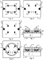
- Fig. 4 is a top down view of a substrate 40 for an array of LED dies 12.
- Fig. 7 shows a cross sectional view of the substrate 40.
- the substrate 40 may include a body 41 formed of aluminum or an alloy for heat sinking.
- the substrate 40 may have any shape, such as rectangular, circular, etc.
- the length or diameter of the substrate 40 depends on the number of LED dies it supports and will typically range from 1 cm to 4 cm.
- the substrate 40 is typically connected in an array of substrates by narrow connectors that are later cut for singulation to simplify handling and speed processing.
- a non-conductive dielectric layer 42 ( Fig. 7 ) is formed over the body 41 for electrical insulation.
- a patterned metal layer such as copper, is formed over the dielectric layer 42 to define small solder pad groups 44A, 44B, 44C, and 44D for each of the LED dies 12 in the array, and to define larger solder pads 46 and 48 for the array's anode and cathode electrodes.
- the solder pad groups 44A-D may include one or more heat sink connections.
- the metal layer also forms interconnections 50 between the LED dies 12 and the electrodes 46 and 48. In the example, only four LED dies 12 are connected in series and parallel. In other embodiments, more or fewer LED dies 12 may be interconnected in series and/or parallel to achieve the desired electrical characteristics and flux.
- a problem with the related prior art LED modules is that a significant portion of the LED light emitted downward is absorbed by the mounting substrate. The most absorption by the substrate occurs in the vicinity of each LED die 12, since that is where the light is the brightest. The present invention minimizes such absorption.
- a white (diffusing) paint 52 is screen printed over the substrate 40 in all places except where solder is to be applied.
- Fig. 7 is a discontinuous cross-section along line 7-7 in Fig. 5 and shows the paint 52 in cross-section.
- the screen is a mesh that is patterned to block the deposition of the white paint 52 over the solder pad groups 44A, 44B, 44C, and 44D.
- the white paint 52 is a viscous dielectric that is then cured. Accordingly, the white paint 52 replaces a conventional solder mask, and no additional steps are required.
- a solder mask restricts any deposited solder, such as molten solder that flows over the substrate 40, to areas that are exposed by the mask.
- Examples of a diffusing white paint include a binder (such as silicone) infused with particles of TiO 2 , ZiO 2 , VO 2 , or other suitable reflective scattering particles.
- the white paint is applied, in conjunction with a mask, by jetting, spraying, a photolithography process with evaporation, or other technique.
- the white paint 52 material should be thermally conductive.
- the reflectivity of the white paint 52 is at least 90% for visible light.
- the white paint 52 as the solder mask, it is ensured that the reflective material extends to the edge of the LED dies 12 and even under the LED dies 12 between the electrodes. Accordingly, the white paint 52 maximizes the reflective surface area of the substrate, limits the applied solder to only the areas exposed by the solder mask, and acts as a corrosion barrier for the metal traces, without any added process steps, so there is synergy in the inventive process.
- a conventional solder mask material (e.g., used for non-LED circuit boards) is applied directly over the substrate 40 followed by the deposition of the white paint 52 (using the same mask pattern) if the conventional solder mask material is desired for adequate protection of the substrate 40 and to reduce costs.
- the white paint 52 protects the solder mask material from degrading due to the high intensity blue or UV light.
- a solder 54 ( Fig. 7 ) is then applied to the various solder pads for wetting.
- the solder 54 may be screen-printed, or applied with a solder mask, or applied in any other conventional way.
- the solder 54 may be a solder paste.
- the LED die 12 electrodes are soldered to the substrate's solder pads using a heating process. As seen, there is no gap between the white paint 52 and the edge of the LED dies 12. If the LED dies were vertical LED dies, only the bottom electrode would be directly soldered to one of the substrate's 42 solder pads, and the top electrode would be wire-bonded to another solder pad. If the LED dies were lateral LED dies, the bottom thermal pad would be soldered to one of the substrate's 42 solder pads and both top electrodes would be wire-bonded to associated solder pads. In virtually all LED dies, there is at least one bottom metal bond pad that serves as an electrical and/or thermal pad.
- solder is not used. Instead the bonding may be by an ultrasonic weld, a conductive adhesive (electrically and thermally conductive), or using other techniques. In such cases, the "solder mask" would be referred to by a suitable name but would still define the areas on the substrate 40 where the bottom metal bond pad of the LED die is to be bonded, and the exposed areas would be approximately the size of the LED die.
- Fig. 7 is a compressed and magnified cross-sectional view of a portion of the substrate 40 along line 7-7 in Fig. 5 cutting across two of the LED dies 12 in the horizontal direction.
- a solder 54 is shown connecting the LED die electrodes to the solder pad groups 44A and 44D.
- Domed lenses 58 may optionally be molded over the LED dies 12 for improved light extraction and protection of the LED dies 12.
- LED dies 12 may be enclosed in domed lens prior to soldering, with or without a submount.
- a reflective ring 60 is affixed to the surface of the substrate 40, surrounding the array of LED dies 12.
- the ring 60 may be a reflective metal or a material coated with a reflective layer.
- the ring 60 may be affixed with silicone or epoxy.
- Fig. 9 is a compressed and magnified cross-sectional view of a portion of the substrate 40 along line 9-9 in Fig. 8 cutting across two of the LED dies 12 in the horizontal direction and the ring 60, where walls of the ring 60 extend above the tops of the LED dies 12 and reflect and mix the light.
- a viscous phosphor mixture 62 is deposited within the ring 60, acting as a mold, and cured.
- the phosphor mixture 62 may be a mixture of silicone and phosphor particles. Many ways to deposit the phosphor mixture 62 are envisioned, such as by using a syringe, screen printing, positioning a pre-formed tablet in the ring that is then melted, etc.
- the phosphor mixture 62 encapsulates the LED dies 12 for added protection.
- the thickness of the phosphor mixture 62 and phosphor particle density are controlled to achieve the desired combination of blue light leakage and phosphor conversion.
- the phosphor may be a single phosphor (e.g., YAG) or a combination of phosphors (e.g., YAG and red, or green and red, etc.) to achieve the desired color emission.
- the indices of refraction of the various layers are selected to provide a transition from the high index GaN to the low index of air to minimize total internal reflection (TIR).
- the reflective surface of the substrate 40 under the phosphor mixture 62 reflects back over 94% of all the phosphor light emitted in a downward direction.
- any number of LED dies 12 may be mounted on the substrate 40, and the diameter of the ring 60 is that needed to surround the LED dies 12 and may be adjusted accordingly. Any number of the resulting substrates 40 can be connected in a system to achieve any desired flux. In one embodiment, the resulting structure emits white light. Other emission colors are possible by selecting different LED dies and phosphors. A quantum dot material may be substituted for the phosphor mixture 62.
Landscapes
- Engineering & Computer Science (AREA)
- Microelectronics & Electronic Packaging (AREA)
- Power Engineering (AREA)
- Computer Hardware Design (AREA)
- Manufacturing & Machinery (AREA)
- Physics & Mathematics (AREA)
- Condensed Matter Physics & Semiconductors (AREA)
- General Physics & Mathematics (AREA)
- Led Device Packages (AREA)
Applications Claiming Priority (2)
| Application Number | Priority Date | Filing Date | Title |
|---|---|---|---|
| US201361917421P | 2013-12-18 | 2013-12-18 | |
| PCT/IB2014/066349 WO2015092579A1 (en) | 2013-12-18 | 2014-11-26 | Reflective solder mask layer for led phosphor package |
Publications (2)
| Publication Number | Publication Date |
|---|---|
| EP3084849A1 EP3084849A1 (en) | 2016-10-26 |
| EP3084849B1 true EP3084849B1 (en) | 2019-10-02 |
Family
ID=52345473
Family Applications (1)
| Application Number | Title | Priority Date | Filing Date |
|---|---|---|---|
| EP14825437.8A Active EP3084849B1 (en) | 2013-12-18 | 2014-11-26 | Reflective solder mask layer for led package and method of fabricating a light emitting structure |
Country Status (6)
| Country | Link |
|---|---|
| US (2) | US10204887B2 (zh) |
| EP (1) | EP3084849B1 (zh) |
| JP (1) | JP6542227B2 (zh) |
| KR (1) | KR102305948B1 (zh) |
| CN (1) | CN105814704A (zh) |
| WO (1) | WO2015092579A1 (zh) |
Families Citing this family (10)
| Publication number | Priority date | Publication date | Assignee | Title |
|---|---|---|---|---|
| JP6542227B2 (ja) | 2013-12-18 | 2019-07-10 | ルミレッズ ホールディング ベーフェー | Led蛍光体パッケージ用の反射性はんだマスク層 |
| WO2017095712A1 (en) * | 2015-12-02 | 2017-06-08 | Koninklijke Philips N.V. | Led metal pad configuration for optimized thermal resistance, solder reliability, and smt processing yields |
| JP2019033160A (ja) * | 2017-08-07 | 2019-02-28 | 株式会社小糸製作所 | 基板および車両用灯具 |
| KR20190019745A (ko) * | 2017-08-18 | 2019-02-27 | 주식회사 루멘스 | 발광소자 및 그 제조방법 |
| US11153976B2 (en) | 2018-05-24 | 2021-10-19 | International Business Machines Corporation | Implementing IR reflective mask to minimize CTE mismatch between laminate and PTH copper |
| EP3598510B1 (en) * | 2018-07-18 | 2022-02-23 | Lumileds LLC | Light emitting diode device and producing methods thereof |
| CN110737137B (zh) * | 2019-10-31 | 2022-09-13 | 厦门天马微电子有限公司 | Led基板及制作方法、背光模组及显示装置 |
| KR20220033521A (ko) * | 2020-04-17 | 2022-03-16 | 닝보 선푸 엘이디 컴퍼니 리미티드 | 자외선 led 장치 |
| US11873954B2 (en) | 2020-09-03 | 2024-01-16 | Signify Holding B.V. | Lighting board and luminaire using the lighting board |
| TWI815639B (zh) * | 2022-09-02 | 2023-09-11 | 矽品精密工業股份有限公司 | 電子封裝件及其製法 |
Citations (2)
| Publication number | Priority date | Publication date | Assignee | Title |
|---|---|---|---|---|
| US20130109136A1 (en) * | 2011-10-31 | 2013-05-02 | Nordson Corporation | Methods of fabricating electronics assemblies |
| US20130328070A1 (en) * | 2012-06-06 | 2013-12-12 | Cree, Inc. | Light emitting devices and substrates with improved plating |
Family Cites Families (40)
| Publication number | Priority date | Publication date | Assignee | Title |
|---|---|---|---|---|
| US6120883A (en) * | 1996-08-19 | 2000-09-19 | Furon Company | Computer printable top coating |
| JP2002314143A (ja) * | 2001-04-09 | 2002-10-25 | Toshiba Corp | 発光装置 |
| US6841623B2 (en) * | 2001-06-29 | 2005-01-11 | Bayer Inc. | Low molecular weight nitrile rubber |
| JP2003185813A (ja) * | 2001-12-21 | 2003-07-03 | Mitsui Chemicals Inc | 反射体およびその用途 |
| US8574959B2 (en) | 2003-11-10 | 2013-11-05 | Stats Chippac, Ltd. | Semiconductor device and method of forming bump-on-lead interconnection |
| TWI534915B (zh) | 2003-11-10 | 2016-05-21 | 恰巴克有限公司 | 引線上凸塊之倒裝晶片互連 |
| US20050270755A1 (en) * | 2004-06-04 | 2005-12-08 | Inventec Corporation | Method for preventing pins of semiconductor package from short circuit during soldering |
| KR101193740B1 (ko) * | 2004-06-30 | 2012-10-22 | 크리 인코포레이티드 | 발광 소자의 패키징을 위한 칩-규모 방법 및 칩 규모로 패키징된 발광 소자 |
| JP2008091459A (ja) * | 2006-09-29 | 2008-04-17 | Rohm Co Ltd | Led照明装置及びその製造方法 |
| US8426740B2 (en) * | 2008-05-29 | 2013-04-23 | Denki Kagaku Kogyo Kabushiki Kaisha | Metal base circuit board |
| WO2009148543A2 (en) * | 2008-05-29 | 2009-12-10 | Cree, Inc. | Light source with near field mixing |
| KR101039957B1 (ko) * | 2008-11-18 | 2011-06-09 | 엘지이노텍 주식회사 | 발광 장치 및 이를 구비한 디스플레이 장치 |
| KR101064026B1 (ko) | 2009-02-17 | 2011-09-08 | 엘지이노텍 주식회사 | 발광 디바이스 패키지 및 그 제조방법 |
| DE202009018419U1 (de) | 2009-03-09 | 2011-08-17 | Tridonic Jennersdorf Gmbh | LED-Modul mit verbesserter Lichtleistung |
| US8184230B2 (en) | 2009-05-08 | 2012-05-22 | Honeywell International Inc. | High efficiency backlight assembly for flat panel display assembly and method for the manufacture thereof |
| US20110049545A1 (en) | 2009-09-02 | 2011-03-03 | Koninklijke Philips Electronics N.V. | Led package with phosphor plate and reflective substrate |
| DE112011100376T5 (de) * | 2010-01-29 | 2012-11-29 | Citizen Electronics Co., Ltd. | Verfahren zur herstellung einer licht aussendenden vorrichtung und licht aussendende vorrichtung |
| US9012938B2 (en) | 2010-04-09 | 2015-04-21 | Cree, Inc. | High reflective substrate of light emitting devices with improved light output |
| US9105824B2 (en) | 2010-04-09 | 2015-08-11 | Cree, Inc. | High reflective board or substrate for LEDs |
| DE102010029368A1 (de) | 2010-05-27 | 2011-12-01 | Osram Opto Semiconductors Gmbh | Elektronische Anordnung und Verfahren zum Herstellen einer elektronischen Anordnung |
| CN102315185A (zh) | 2010-06-29 | 2012-01-11 | 昆山旭扬电子材料有限公司 | 电子组件模块 |
| WO2012016226A1 (en) * | 2010-07-30 | 2012-02-02 | Bytemobile, Inc. | Systems and methods for video cache indexing |
| JP2012089357A (ja) * | 2010-10-20 | 2012-05-10 | Sumitomo Light Metal Ind Ltd | Led照明基板用積層体及びそれを用いたled照明 |
| TWI441361B (zh) | 2010-12-31 | 2014-06-11 | Interlight Optotech Corp | 發光二極體封裝結構及其製造方法 |
| US9461023B2 (en) | 2011-10-28 | 2016-10-04 | Bridgelux, Inc. | Jetting a highly reflective layer onto an LED assembly |
| JP5673190B2 (ja) | 2011-02-18 | 2015-02-18 | 日亜化学工業株式会社 | 発光装置 |
| EP2500623A1 (en) * | 2011-03-18 | 2012-09-19 | Koninklijke Philips Electronics N.V. | Method for providing a reflective coating to a substrate for a light-emitting device |
| JP5670250B2 (ja) | 2011-04-18 | 2015-02-18 | イビデン株式会社 | Led基板、発光モジュール、発光モジュールを有する機器、led基板の製造方法、発光モジュールの製造方法、及び発光モジュールを有する機器の製造方法 |
| JP2012243846A (ja) | 2011-05-17 | 2012-12-10 | Sumitomo Chemical Co Ltd | 金属ベース回路基板および発光素子 |
| CN103650181A (zh) | 2011-06-29 | 2014-03-19 | 松下电器产业株式会社 | 发光装置 |
| KR101850431B1 (ko) * | 2011-07-07 | 2018-05-31 | 엘지이노텍 주식회사 | 발광 모듈 및 이를 포함하는 조명 시스템 |
| KR101246087B1 (ko) * | 2011-07-08 | 2013-03-21 | 한전원자력연료 주식회사 | 솔레노이드 밸브 박스를 내장한 핵연료 집합체의 성능 검사 테이블 |
| JP2013033843A (ja) * | 2011-08-02 | 2013-02-14 | Sony Corp | 回路基板、回路基板の製造方法、表示装置および電子機器 |
| US20130032211A1 (en) * | 2011-08-03 | 2013-02-07 | National Tsing Hua University | Air Compression System Having Characteristic of Storing Unstable Energy and Method for Controlling the Same |
| KR101142434B1 (ko) * | 2011-09-08 | 2012-05-08 | (주)오비메드 | 조기양막파수 산모에서 비침습적인 양수 내 염증 및 감염의 예측 또는 진단 방법 |
| JP2013135084A (ja) | 2011-12-26 | 2013-07-08 | Nitto Denko Corp | 発光ダイオード装置の製造方法 |
| US8541802B2 (en) * | 2012-01-31 | 2013-09-24 | Bridgelux, Inc. | Phosphor placement in white light emitting diode assemblies |
| US20130264970A1 (en) | 2012-04-06 | 2013-10-10 | Yew Cheong Kuan | Light emitting diode (led) components and methods for improved light extraction |
| US9383496B2 (en) * | 2012-06-05 | 2016-07-05 | Rambus Delaware Llc | Edge lit lighting assembly with spectrum adjuster |
| JP6542227B2 (ja) | 2013-12-18 | 2019-07-10 | ルミレッズ ホールディング ベーフェー | Led蛍光体パッケージ用の反射性はんだマスク層 |
-
2014
- 2014-11-26 JP JP2016540036A patent/JP6542227B2/ja active Active
- 2014-11-26 CN CN201480069463.1A patent/CN105814704A/zh active Pending
- 2014-11-26 WO PCT/IB2014/066349 patent/WO2015092579A1/en active Application Filing
- 2014-11-26 US US15/103,474 patent/US10204887B2/en active Active
- 2014-11-26 EP EP14825437.8A patent/EP3084849B1/en active Active
- 2014-11-26 KR KR1020167019152A patent/KR102305948B1/ko active IP Right Grant
-
2019
- 2019-02-05 US US16/268,097 patent/US11189601B2/en active Active
Patent Citations (2)
| Publication number | Priority date | Publication date | Assignee | Title |
|---|---|---|---|---|
| US20130109136A1 (en) * | 2011-10-31 | 2013-05-02 | Nordson Corporation | Methods of fabricating electronics assemblies |
| US20130328070A1 (en) * | 2012-06-06 | 2013-12-12 | Cree, Inc. | Light emitting devices and substrates with improved plating |
Also Published As
| Publication number | Publication date |
|---|---|
| JP6542227B2 (ja) | 2019-07-10 |
| JP2017501578A (ja) | 2017-01-12 |
| US11189601B2 (en) | 2021-11-30 |
| KR102305948B1 (ko) | 2021-09-28 |
| EP3084849A1 (en) | 2016-10-26 |
| CN105814704A (zh) | 2016-07-27 |
| KR20160101056A (ko) | 2016-08-24 |
| WO2015092579A1 (en) | 2015-06-25 |
| US20160315069A1 (en) | 2016-10-27 |
| US20190304956A1 (en) | 2019-10-03 |
| US10204887B2 (en) | 2019-02-12 |
Similar Documents
| Publication | Publication Date | Title |
|---|---|---|
| US11189601B2 (en) | Reflective solder mask layer for LED phosphor package | |
| JP4791381B2 (ja) | 発光デバイスの製造方法 | |
| US8791471B2 (en) | Multi-chip light emitting diode modules | |
| TWI400819B (zh) | 用於線光源之發光二極體模組 | |
| JP5842813B2 (ja) | 発光装置および発光装置の製造方法 | |
| US9512968B2 (en) | LED module | |
| JP6354273B2 (ja) | 発光装置及び発光装置の製造方法 | |
| US20160005939A1 (en) | Light emitting diode (led) components including contact expansion frame and methods of fabricating same | |
| US20180226552A1 (en) | Light-emitting element package | |
| KR20110000730A (ko) | 표면 실장 led 모듈 및 표면 실장 led 모듈의 제조 방법 | |
| EP2745320B1 (en) | Led mixing chamber with reflective walls formed in slots | |
| JP6964345B2 (ja) | 発光素子パッケージ及び光源装置 | |
| EP2312657A1 (en) | Light emitting diode device, light emitting apparatus and method of manufacturing light emitting diode device | |
| US20160079483A1 (en) | Light-emitting unit and semiconductor light-emitting device | |
| US9117689B2 (en) | Light emitting device and manufacturing method thereof | |
| TW201349598A (zh) | 發光半導體元件及其製作方法 | |
| US10355180B2 (en) | Light emitting device and light emitting module | |
| US20150200336A1 (en) | Wafer level contact pad standoffs with integrated reflector | |
| US20220102599A1 (en) | Deep molded reflector cup used as complete led package | |
| US9029902B2 (en) | Optoelectronic semiconductor device comprising a semiconductor chip, a carrier substrate and a film | |
| CN110085729B (zh) | 光源模块 | |
| US9954144B2 (en) | Wafer level contact pad solder bumping for surface mount devices with non-planar recessed contacting surfaces | |
| CN117832209A (zh) | 发光模组及显示装置 | |
| KR20150142121A (ko) | 반도체 발광소자 |
Legal Events
| Date | Code | Title | Description |
|---|---|---|---|
| PUAI | Public reference made under article 153(3) epc to a published international application that has entered the european phase |
Free format text: ORIGINAL CODE: 0009012 |
|
| 17P | Request for examination filed |
Effective date: 20160718 |
|
| AK | Designated contracting states |
Kind code of ref document: A1 Designated state(s): AL AT BE BG CH CY CZ DE DK EE ES FI FR GB GR HR HU IE IS IT LI LT LU LV MC MK MT NL NO PL PT RO RS SE SI SK SM TR |
|
| AX | Request for extension of the european patent |
Extension state: BA ME |
|
| DAX | Request for extension of the european patent (deleted) | ||
| STAA | Information on the status of an ep patent application or granted ep patent |
Free format text: STATUS: EXAMINATION IS IN PROGRESS |
|
| 17Q | First examination report despatched |
Effective date: 20180423 |
|
| RAP1 | Party data changed (applicant data changed or rights of an application transferred) |
Owner name: LUMILEDS HOLDING B.V. |
|
| RAP1 | Party data changed (applicant data changed or rights of an application transferred) |
Owner name: LUMILEDS HOLDING B.V. |
|
| GRAP | Despatch of communication of intention to grant a patent |
Free format text: ORIGINAL CODE: EPIDOSNIGR1 |
|
| STAA | Information on the status of an ep patent application or granted ep patent |
Free format text: STATUS: GRANT OF PATENT IS INTENDED |
|
| RIC1 | Information provided on ipc code assigned before grant |
Ipc: H01L 33/60 20100101AFI20190529BHEP Ipc: H01L 33/62 20100101ALN20190529BHEP |
|
| RIC1 | Information provided on ipc code assigned before grant |
Ipc: H01L 33/62 20100101ALN20190605BHEP Ipc: H01L 33/60 20100101AFI20190605BHEP |
|
| INTG | Intention to grant announced |
Effective date: 20190619 |
|
| GRAS | Grant fee paid |
Free format text: ORIGINAL CODE: EPIDOSNIGR3 |
|
| GRAA | (expected) grant |
Free format text: ORIGINAL CODE: 0009210 |
|
| STAA | Information on the status of an ep patent application or granted ep patent |
Free format text: STATUS: THE PATENT HAS BEEN GRANTED |
|
| AK | Designated contracting states |
Kind code of ref document: B1 Designated state(s): AL AT BE BG CH CY CZ DE DK EE ES FI FR GB GR HR HU IE IS IT LI LT LU LV MC MK MT NL NO PL PT RO RS SE SI SK SM TR |
|
| REG | Reference to a national code |
Ref country code: GB Ref legal event code: FG4D |
|
| REG | Reference to a national code |
Ref country code: CH Ref legal event code: EP Ref country code: AT Ref legal event code: REF Ref document number: 1187165 Country of ref document: AT Kind code of ref document: T Effective date: 20191015 |
|
| REG | Reference to a national code |
Ref country code: DE Ref legal event code: R096 Ref document number: 602014054688 Country of ref document: DE |
|
| REG | Reference to a national code |
Ref country code: IE Ref legal event code: FG4D |
|
| REG | Reference to a national code |
Ref country code: NL Ref legal event code: MP Effective date: 20191002 |
|
| REG | Reference to a national code |
Ref country code: LT Ref legal event code: MG4D |
|
| REG | Reference to a national code |
Ref country code: AT Ref legal event code: MK05 Ref document number: 1187165 Country of ref document: AT Kind code of ref document: T Effective date: 20191002 |
|
| PG25 | Lapsed in a contracting state [announced via postgrant information from national office to epo] |
Ref country code: LT Free format text: LAPSE BECAUSE OF FAILURE TO SUBMIT A TRANSLATION OF THE DESCRIPTION OR TO PAY THE FEE WITHIN THE PRESCRIBED TIME-LIMIT Effective date: 20191002 Ref country code: PL Free format text: LAPSE BECAUSE OF FAILURE TO SUBMIT A TRANSLATION OF THE DESCRIPTION OR TO PAY THE FEE WITHIN THE PRESCRIBED TIME-LIMIT Effective date: 20191002 Ref country code: NO Free format text: LAPSE BECAUSE OF FAILURE TO SUBMIT A TRANSLATION OF THE DESCRIPTION OR TO PAY THE FEE WITHIN THE PRESCRIBED TIME-LIMIT Effective date: 20200102 Ref country code: NL Free format text: LAPSE BECAUSE OF FAILURE TO SUBMIT A TRANSLATION OF THE DESCRIPTION OR TO PAY THE FEE WITHIN THE PRESCRIBED TIME-LIMIT Effective date: 20191002 Ref country code: SE Free format text: LAPSE BECAUSE OF FAILURE TO SUBMIT A TRANSLATION OF THE DESCRIPTION OR TO PAY THE FEE WITHIN THE PRESCRIBED TIME-LIMIT Effective date: 20191002 Ref country code: LV Free format text: LAPSE BECAUSE OF FAILURE TO SUBMIT A TRANSLATION OF THE DESCRIPTION OR TO PAY THE FEE WITHIN THE PRESCRIBED TIME-LIMIT Effective date: 20191002 Ref country code: PT Free format text: LAPSE BECAUSE OF FAILURE TO SUBMIT A TRANSLATION OF THE DESCRIPTION OR TO PAY THE FEE WITHIN THE PRESCRIBED TIME-LIMIT Effective date: 20200203 Ref country code: BG Free format text: LAPSE BECAUSE OF FAILURE TO SUBMIT A TRANSLATION OF THE DESCRIPTION OR TO PAY THE FEE WITHIN THE PRESCRIBED TIME-LIMIT Effective date: 20200102 Ref country code: FI Free format text: LAPSE BECAUSE OF FAILURE TO SUBMIT A TRANSLATION OF THE DESCRIPTION OR TO PAY THE FEE WITHIN THE PRESCRIBED TIME-LIMIT Effective date: 20191002 Ref country code: AT Free format text: LAPSE BECAUSE OF FAILURE TO SUBMIT A TRANSLATION OF THE DESCRIPTION OR TO PAY THE FEE WITHIN THE PRESCRIBED TIME-LIMIT Effective date: 20191002 Ref country code: ES Free format text: LAPSE BECAUSE OF FAILURE TO SUBMIT A TRANSLATION OF THE DESCRIPTION OR TO PAY THE FEE WITHIN THE PRESCRIBED TIME-LIMIT Effective date: 20191002 Ref country code: GR Free format text: LAPSE BECAUSE OF FAILURE TO SUBMIT A TRANSLATION OF THE DESCRIPTION OR TO PAY THE FEE WITHIN THE PRESCRIBED TIME-LIMIT Effective date: 20200103 |
|
| PG25 | Lapsed in a contracting state [announced via postgrant information from national office to epo] |
Ref country code: IS Free format text: LAPSE BECAUSE OF FAILURE TO SUBMIT A TRANSLATION OF THE DESCRIPTION OR TO PAY THE FEE WITHIN THE PRESCRIBED TIME-LIMIT Effective date: 20200224 Ref country code: HR Free format text: LAPSE BECAUSE OF FAILURE TO SUBMIT A TRANSLATION OF THE DESCRIPTION OR TO PAY THE FEE WITHIN THE PRESCRIBED TIME-LIMIT Effective date: 20191002 Ref country code: CZ Free format text: LAPSE BECAUSE OF FAILURE TO SUBMIT A TRANSLATION OF THE DESCRIPTION OR TO PAY THE FEE WITHIN THE PRESCRIBED TIME-LIMIT Effective date: 20191002 Ref country code: RS Free format text: LAPSE BECAUSE OF FAILURE TO SUBMIT A TRANSLATION OF THE DESCRIPTION OR TO PAY THE FEE WITHIN THE PRESCRIBED TIME-LIMIT Effective date: 20191002 |
|
| PG25 | Lapsed in a contracting state [announced via postgrant information from national office to epo] |
Ref country code: AL Free format text: LAPSE BECAUSE OF FAILURE TO SUBMIT A TRANSLATION OF THE DESCRIPTION OR TO PAY THE FEE WITHIN THE PRESCRIBED TIME-LIMIT Effective date: 20191002 |
|
| REG | Reference to a national code |
Ref country code: CH Ref legal event code: PL |
|
| REG | Reference to a national code |
Ref country code: DE Ref legal event code: R097 Ref document number: 602014054688 Country of ref document: DE |
|
| PG2D | Information on lapse in contracting state deleted |
Ref country code: IS |
|
| PG25 | Lapsed in a contracting state [announced via postgrant information from national office to epo] |
Ref country code: MC Free format text: LAPSE BECAUSE OF FAILURE TO SUBMIT A TRANSLATION OF THE DESCRIPTION OR TO PAY THE FEE WITHIN THE PRESCRIBED TIME-LIMIT Effective date: 20191002 Ref country code: LU Free format text: LAPSE BECAUSE OF NON-PAYMENT OF DUE FEES Effective date: 20191126 Ref country code: RO Free format text: LAPSE BECAUSE OF FAILURE TO SUBMIT A TRANSLATION OF THE DESCRIPTION OR TO PAY THE FEE WITHIN THE PRESCRIBED TIME-LIMIT Effective date: 20191002 Ref country code: CH Free format text: LAPSE BECAUSE OF NON-PAYMENT OF DUE FEES Effective date: 20191130 Ref country code: EE Free format text: LAPSE BECAUSE OF FAILURE TO SUBMIT A TRANSLATION OF THE DESCRIPTION OR TO PAY THE FEE WITHIN THE PRESCRIBED TIME-LIMIT Effective date: 20191002 Ref country code: DK Free format text: LAPSE BECAUSE OF FAILURE TO SUBMIT A TRANSLATION OF THE DESCRIPTION OR TO PAY THE FEE WITHIN THE PRESCRIBED TIME-LIMIT Effective date: 20191002 Ref country code: LI Free format text: LAPSE BECAUSE OF NON-PAYMENT OF DUE FEES Effective date: 20191130 Ref country code: IS Free format text: LAPSE BECAUSE OF FAILURE TO SUBMIT A TRANSLATION OF THE DESCRIPTION OR TO PAY THE FEE WITHIN THE PRESCRIBED TIME-LIMIT Effective date: 20200202 |
|
| PLBE | No opposition filed within time limit |
Free format text: ORIGINAL CODE: 0009261 |
|
| STAA | Information on the status of an ep patent application or granted ep patent |
Free format text: STATUS: NO OPPOSITION FILED WITHIN TIME LIMIT |
|
| REG | Reference to a national code |
Ref country code: BE Ref legal event code: MM Effective date: 20191130 |
|
| PG25 | Lapsed in a contracting state [announced via postgrant information from national office to epo] |
Ref country code: IT Free format text: LAPSE BECAUSE OF FAILURE TO SUBMIT A TRANSLATION OF THE DESCRIPTION OR TO PAY THE FEE WITHIN THE PRESCRIBED TIME-LIMIT Effective date: 20191002 Ref country code: SM Free format text: LAPSE BECAUSE OF FAILURE TO SUBMIT A TRANSLATION OF THE DESCRIPTION OR TO PAY THE FEE WITHIN THE PRESCRIBED TIME-LIMIT Effective date: 20191002 Ref country code: SK Free format text: LAPSE BECAUSE OF FAILURE TO SUBMIT A TRANSLATION OF THE DESCRIPTION OR TO PAY THE FEE WITHIN THE PRESCRIBED TIME-LIMIT Effective date: 20191002 |
|
| 26N | No opposition filed |
Effective date: 20200703 |
|
| PG25 | Lapsed in a contracting state [announced via postgrant information from national office to epo] |
Ref country code: IE Free format text: LAPSE BECAUSE OF NON-PAYMENT OF DUE FEES Effective date: 20191126 |
|
| PG25 | Lapsed in a contracting state [announced via postgrant information from national office to epo] |
Ref country code: BE Free format text: LAPSE BECAUSE OF NON-PAYMENT OF DUE FEES Effective date: 20191130 Ref country code: SI Free format text: LAPSE BECAUSE OF FAILURE TO SUBMIT A TRANSLATION OF THE DESCRIPTION OR TO PAY THE FEE WITHIN THE PRESCRIBED TIME-LIMIT Effective date: 20191002 |
|
| PG25 | Lapsed in a contracting state [announced via postgrant information from national office to epo] |
Ref country code: CY Free format text: LAPSE BECAUSE OF FAILURE TO SUBMIT A TRANSLATION OF THE DESCRIPTION OR TO PAY THE FEE WITHIN THE PRESCRIBED TIME-LIMIT Effective date: 20191002 |
|
| PG25 | Lapsed in a contracting state [announced via postgrant information from national office to epo] |
Ref country code: MT Free format text: LAPSE BECAUSE OF FAILURE TO SUBMIT A TRANSLATION OF THE DESCRIPTION OR TO PAY THE FEE WITHIN THE PRESCRIBED TIME-LIMIT Effective date: 20191002 Ref country code: HU Free format text: LAPSE BECAUSE OF FAILURE TO SUBMIT A TRANSLATION OF THE DESCRIPTION OR TO PAY THE FEE WITHIN THE PRESCRIBED TIME-LIMIT; INVALID AB INITIO Effective date: 20141126 |
|
| PG25 | Lapsed in a contracting state [announced via postgrant information from national office to epo] |
Ref country code: TR Free format text: LAPSE BECAUSE OF FAILURE TO SUBMIT A TRANSLATION OF THE DESCRIPTION OR TO PAY THE FEE WITHIN THE PRESCRIBED TIME-LIMIT Effective date: 20191002 |
|
| PG25 | Lapsed in a contracting state [announced via postgrant information from national office to epo] |
Ref country code: MK Free format text: LAPSE BECAUSE OF FAILURE TO SUBMIT A TRANSLATION OF THE DESCRIPTION OR TO PAY THE FEE WITHIN THE PRESCRIBED TIME-LIMIT Effective date: 20191002 |
|
| P01 | Opt-out of the competence of the unified patent court (upc) registered |
Effective date: 20230530 |
|
| PGFP | Annual fee paid to national office [announced via postgrant information from national office to epo] |
Ref country code: GB Payment date: 20231121 Year of fee payment: 10 |
|
| PGFP | Annual fee paid to national office [announced via postgrant information from national office to epo] |
Ref country code: FR Payment date: 20231123 Year of fee payment: 10 Ref country code: DE Payment date: 20231127 Year of fee payment: 10 |