EP3084810B1 - Interconnexions à base de cobalt et procédés pour leur fabrication - Google Patents
Interconnexions à base de cobalt et procédés pour leur fabrication Download PDFInfo
- Publication number
- EP3084810B1 EP3084810B1 EP15729733.4A EP15729733A EP3084810B1 EP 3084810 B1 EP3084810 B1 EP 3084810B1 EP 15729733 A EP15729733 A EP 15729733A EP 3084810 B1 EP3084810 B1 EP 3084810B1
- Authority
- EP
- European Patent Office
- Prior art keywords
- layer
- fill material
- cobalt
- adhesion layer
- opening
- Prior art date
- Legal status (The legal status is an assumption and is not a legal conclusion. Google has not performed a legal analysis and makes no representation as to the accuracy of the status listed.)
- Active
Links
- GUTLYIVDDKVIGB-UHFFFAOYSA-N cobalt atom Chemical compound [Co] GUTLYIVDDKVIGB-UHFFFAOYSA-N 0.000 title claims description 135
- 229910017052 cobalt Inorganic materials 0.000 title claims description 134
- 239000010941 cobalt Substances 0.000 title claims description 134
- 238000000034 method Methods 0.000 title claims description 107
- 238000004519 manufacturing process Methods 0.000 title description 6
- 239000000463 material Substances 0.000 claims description 178
- 239000011572 manganese Substances 0.000 claims description 100
- 229910052748 manganese Inorganic materials 0.000 claims description 57
- PWHULOQIROXLJO-UHFFFAOYSA-N Manganese Chemical compound [Mn] PWHULOQIROXLJO-UHFFFAOYSA-N 0.000 claims description 52
- 239000000758 substrate Substances 0.000 claims description 45
- 229910052751 metal Inorganic materials 0.000 claims description 38
- 239000002184 metal Substances 0.000 claims description 38
- 229910052710 silicon Inorganic materials 0.000 claims description 22
- 239000010703 silicon Substances 0.000 claims description 16
- XUIMIQQOPSSXEZ-UHFFFAOYSA-N Silicon Chemical compound [Si] XUIMIQQOPSSXEZ-UHFFFAOYSA-N 0.000 claims description 15
- 229910052799 carbon Inorganic materials 0.000 claims description 14
- 239000000203 mixture Substances 0.000 claims description 14
- 229910052757 nitrogen Inorganic materials 0.000 claims description 14
- IJGRMHOSHXDMSA-UHFFFAOYSA-N Atomic nitrogen Chemical compound N#N IJGRMHOSHXDMSA-UHFFFAOYSA-N 0.000 claims description 12
- 229910052802 copper Inorganic materials 0.000 claims description 12
- 229910052721 tungsten Inorganic materials 0.000 claims description 11
- 229910052732 germanium Inorganic materials 0.000 claims description 9
- 229910052760 oxygen Inorganic materials 0.000 claims description 9
- 229910052739 hydrogen Inorganic materials 0.000 claims description 7
- WPBNNNQJVZRUHP-UHFFFAOYSA-L manganese(2+);methyl n-[[2-(methoxycarbonylcarbamothioylamino)phenyl]carbamothioyl]carbamate;n-[2-(sulfidocarbothioylamino)ethyl]carbamodithioate Chemical compound [Mn+2].[S-]C(=S)NCCNC([S-])=S.COC(=O)NC(=S)NC1=CC=CC=C1NC(=S)NC(=O)OC WPBNNNQJVZRUHP-UHFFFAOYSA-L 0.000 claims description 7
- 239000001257 hydrogen Substances 0.000 claims description 6
- 125000004435 hydrogen atom Chemical class [H]* 0.000 claims description 6
- 229910052759 nickel Inorganic materials 0.000 claims description 6
- 229910052719 titanium Inorganic materials 0.000 claims description 6
- 229910052782 aluminium Inorganic materials 0.000 claims description 5
- 229910052790 beryllium Inorganic materials 0.000 claims description 5
- 229910052796 boron Inorganic materials 0.000 claims description 5
- 229910052793 cadmium Inorganic materials 0.000 claims description 5
- 229910052791 calcium Inorganic materials 0.000 claims description 5
- 229910052804 chromium Inorganic materials 0.000 claims description 5
- 229910052735 hafnium Inorganic materials 0.000 claims description 5
- 229910052738 indium Inorganic materials 0.000 claims description 5
- 229910052741 iridium Inorganic materials 0.000 claims description 5
- 229910052749 magnesium Inorganic materials 0.000 claims description 5
- 229910052750 molybdenum Inorganic materials 0.000 claims description 5
- 229910052758 niobium Inorganic materials 0.000 claims description 5
- 229910052697 platinum Inorganic materials 0.000 claims description 5
- 229910052702 rhenium Inorganic materials 0.000 claims description 5
- 229910052703 rhodium Inorganic materials 0.000 claims description 5
- 229910052709 silver Inorganic materials 0.000 claims description 5
- 229910052718 tin Inorganic materials 0.000 claims description 5
- 229910052720 vanadium Inorganic materials 0.000 claims description 5
- 229910052725 zinc Inorganic materials 0.000 claims description 5
- 229910052726 zirconium Inorganic materials 0.000 claims description 5
- OKTJSMMVPCPJKN-UHFFFAOYSA-N Carbon Chemical compound [C] OKTJSMMVPCPJKN-UHFFFAOYSA-N 0.000 claims description 3
- QVGXLLKOCUKJST-UHFFFAOYSA-N atomic oxygen Chemical compound [O] QVGXLLKOCUKJST-UHFFFAOYSA-N 0.000 claims description 3
- 239000001301 oxygen Substances 0.000 claims description 3
- 229910052763 palladium Inorganic materials 0.000 claims description 2
- 239000010410 layer Substances 0.000 description 287
- 230000008569 process Effects 0.000 description 71
- 238000000151 deposition Methods 0.000 description 36
- 230000008021 deposition Effects 0.000 description 32
- 239000004065 semiconductor Substances 0.000 description 16
- 238000005240 physical vapour deposition Methods 0.000 description 14
- 239000012790 adhesive layer Substances 0.000 description 13
- 239000010949 copper Substances 0.000 description 12
- 238000000231 atomic layer deposition Methods 0.000 description 11
- 238000005229 chemical vapour deposition Methods 0.000 description 11
- 238000009792 diffusion process Methods 0.000 description 11
- 230000004888 barrier function Effects 0.000 description 10
- 229910017043 MnSix Inorganic materials 0.000 description 9
- 239000000956 alloy Substances 0.000 description 9
- RRZKHZBOZDIQJG-UHFFFAOYSA-N azane;manganese Chemical compound N.[Mn] RRZKHZBOZDIQJG-UHFFFAOYSA-N 0.000 description 9
- 230000008018 melting Effects 0.000 description 9
- 238000002844 melting Methods 0.000 description 9
- 229910045601 alloy Inorganic materials 0.000 description 8
- 238000001465 metallisation Methods 0.000 description 8
- RYGMFSIKBFXOCR-UHFFFAOYSA-N Copper Chemical compound [Cu] RYGMFSIKBFXOCR-UHFFFAOYSA-N 0.000 description 7
- 239000010408 film Substances 0.000 description 7
- 238000012545 processing Methods 0.000 description 7
- 229910052715 tantalum Inorganic materials 0.000 description 7
- GUVRBAGPIYLISA-UHFFFAOYSA-N tantalum atom Chemical compound [Ta] GUVRBAGPIYLISA-UHFFFAOYSA-N 0.000 description 7
- 239000010409 thin film Substances 0.000 description 7
- XKRFYHLGVUSROY-UHFFFAOYSA-N Argon Chemical compound [Ar] XKRFYHLGVUSROY-UHFFFAOYSA-N 0.000 description 6
- 238000013459 approach Methods 0.000 description 6
- 230000015572 biosynthetic process Effects 0.000 description 6
- WFKWXMTUELFFGS-UHFFFAOYSA-N tungsten Chemical compound [W] WFKWXMTUELFFGS-UHFFFAOYSA-N 0.000 description 6
- 239000010937 tungsten Substances 0.000 description 6
- 239000002019 doping agent Substances 0.000 description 5
- -1 for example Substances 0.000 description 5
- 238000013508 migration Methods 0.000 description 5
- 230000005012 migration Effects 0.000 description 5
- PXHVJJICTQNCMI-UHFFFAOYSA-N nickel Substances [Ni] PXHVJJICTQNCMI-UHFFFAOYSA-N 0.000 description 5
- 239000010936 titanium Substances 0.000 description 5
- 238000009736 wetting Methods 0.000 description 5
- 238000005137 deposition process Methods 0.000 description 4
- 230000009977 dual effect Effects 0.000 description 4
- 238000009713 electroplating Methods 0.000 description 4
- GNPVGFCGXDBREM-UHFFFAOYSA-N germanium atom Chemical compound [Ge] GNPVGFCGXDBREM-UHFFFAOYSA-N 0.000 description 4
- 229910021332 silicide Inorganic materials 0.000 description 4
- FVBUAEGBCNSCDD-UHFFFAOYSA-N silicide(4-) Chemical compound [Si-4] FVBUAEGBCNSCDD-UHFFFAOYSA-N 0.000 description 4
- 239000010944 silver (metal) Substances 0.000 description 4
- 229910052786 argon Inorganic materials 0.000 description 3
- 150000001875 compounds Chemical class 0.000 description 3
- 230000001351 cycling effect Effects 0.000 description 3
- 230000003247 decreasing effect Effects 0.000 description 3
- 239000003989 dielectric material Substances 0.000 description 3
- 230000006870 function Effects 0.000 description 3
- 239000012535 impurity Substances 0.000 description 3
- 229910052909 inorganic silicate Inorganic materials 0.000 description 3
- 229910052883 rhodonite Inorganic materials 0.000 description 3
- 150000004760 silicates Chemical class 0.000 description 3
- 239000007787 solid Substances 0.000 description 3
- BPQQTUXANYXVAA-UHFFFAOYSA-N Orthosilicate Chemical compound [O-][Si]([O-])([O-])[O-] BPQQTUXANYXVAA-UHFFFAOYSA-N 0.000 description 2
- 229910052581 Si3N4 Inorganic materials 0.000 description 2
- VYPSYNLAJGMNEJ-UHFFFAOYSA-N Silicium dioxide Chemical compound O=[Si]=O VYPSYNLAJGMNEJ-UHFFFAOYSA-N 0.000 description 2
- 229910000577 Silicon-germanium Inorganic materials 0.000 description 2
- LEVVHYCKPQWKOP-UHFFFAOYSA-N [Si].[Ge] Chemical compound [Si].[Ge] LEVVHYCKPQWKOP-UHFFFAOYSA-N 0.000 description 2
- 125000004429 atom Chemical group 0.000 description 2
- 230000008901 benefit Effects 0.000 description 2
- DDHRUTNUHBNAHW-UHFFFAOYSA-N cobalt germanium Chemical compound [Co].[Ge] DDHRUTNUHBNAHW-UHFFFAOYSA-N 0.000 description 2
- 238000001514 detection method Methods 0.000 description 2
- 238000007772 electroless plating Methods 0.000 description 2
- 230000005669 field effect Effects 0.000 description 2
- 239000007789 gas Substances 0.000 description 2
- SCCCLDWUZODEKG-UHFFFAOYSA-N germanide Chemical compound [GeH3-] SCCCLDWUZODEKG-UHFFFAOYSA-N 0.000 description 2
- 239000011229 interlayer Substances 0.000 description 2
- 238000010849 ion bombardment Methods 0.000 description 2
- 238000002955 isolation Methods 0.000 description 2
- 230000015654 memory Effects 0.000 description 2
- 229910044991 metal oxide Inorganic materials 0.000 description 2
- 150000004706 metal oxides Chemical class 0.000 description 2
- 230000002265 prevention Effects 0.000 description 2
- MZLGASXMSKOWSE-UHFFFAOYSA-N tantalum nitride Chemical compound [Ta]#N MZLGASXMSKOWSE-UHFFFAOYSA-N 0.000 description 2
- 229910000531 Co alloy Inorganic materials 0.000 description 1
- 229910016803 Mn4N Inorganic materials 0.000 description 1
- 229910020177 SiOF Inorganic materials 0.000 description 1
- RTAQQCXQSZGOHL-UHFFFAOYSA-N Titanium Chemical compound [Ti] RTAQQCXQSZGOHL-UHFFFAOYSA-N 0.000 description 1
- NRTOMJZYCJJWKI-UHFFFAOYSA-N Titanium nitride Chemical compound [Ti]#N NRTOMJZYCJJWKI-UHFFFAOYSA-N 0.000 description 1
- 239000000853 adhesive Substances 0.000 description 1
- 230000001070 adhesive effect Effects 0.000 description 1
- 238000005275 alloying Methods 0.000 description 1
- 230000009286 beneficial effect Effects 0.000 description 1
- 230000005540 biological transmission Effects 0.000 description 1
- 239000003990 capacitor Substances 0.000 description 1
- 230000001413 cellular effect Effects 0.000 description 1
- 230000008859 change Effects 0.000 description 1
- 238000005352 clarification Methods 0.000 description 1
- 238000011109 contamination Methods 0.000 description 1
- 229910021419 crystalline silicon Inorganic materials 0.000 description 1
- 230000001627 detrimental effect Effects 0.000 description 1
- 230000000694 effects Effects 0.000 description 1
- 239000011521 glass Substances 0.000 description 1
- 238000011065 in-situ storage Methods 0.000 description 1
- 230000001939 inductive effect Effects 0.000 description 1
- 239000011810 insulating material Substances 0.000 description 1
- 238000001459 lithography Methods 0.000 description 1
- PYLLWONICXJARP-UHFFFAOYSA-N manganese silicon Chemical compound [Si].[Mn] PYLLWONICXJARP-UHFFFAOYSA-N 0.000 description 1
- 238000004377 microelectronic Methods 0.000 description 1
- 238000012986 modification Methods 0.000 description 1
- 230000004048 modification Effects 0.000 description 1
- 150000004767 nitrides Chemical class 0.000 description 1
- 230000003287 optical effect Effects 0.000 description 1
- 238000004806 packaging method and process Methods 0.000 description 1
- 238000007747 plating Methods 0.000 description 1
- 239000002861 polymer material Substances 0.000 description 1
- 239000002096 quantum dot Substances 0.000 description 1
- 239000000523 sample Substances 0.000 description 1
- 230000035945 sensitivity Effects 0.000 description 1
- 235000012239 silicon dioxide Nutrition 0.000 description 1
- 239000000377 silicon dioxide Substances 0.000 description 1
- HQVNEWCFYHHQES-UHFFFAOYSA-N silicon nitride Chemical compound N12[Si]34N5[Si]62N3[Si]51N64 HQVNEWCFYHHQES-UHFFFAOYSA-N 0.000 description 1
- 239000002356 single layer Substances 0.000 description 1
- 125000006850 spacer group Chemical group 0.000 description 1
- 239000000126 substance Substances 0.000 description 1
- 238000006467 substitution reaction Methods 0.000 description 1
- 239000011800 void material Substances 0.000 description 1
Images


Classifications
-
- H—ELECTRICITY
- H01—ELECTRIC ELEMENTS
- H01L—SEMICONDUCTOR DEVICES NOT COVERED BY CLASS H10
- H01L23/00—Details of semiconductor or other solid state devices
- H01L23/52—Arrangements for conducting electric current within the device in operation from one component to another, i.e. interconnections, e.g. wires, lead frames
- H01L23/522—Arrangements for conducting electric current within the device in operation from one component to another, i.e. interconnections, e.g. wires, lead frames including external interconnections consisting of a multilayer structure of conductive and insulating layers inseparably formed on the semiconductor body
- H01L23/532—Arrangements for conducting electric current within the device in operation from one component to another, i.e. interconnections, e.g. wires, lead frames including external interconnections consisting of a multilayer structure of conductive and insulating layers inseparably formed on the semiconductor body characterised by the materials
- H01L23/53204—Conductive materials
- H01L23/53209—Conductive materials based on metals, e.g. alloys, metal silicides
- H01L23/53257—Conductive materials based on metals, e.g. alloys, metal silicides the principal metal being a refractory metal
- H01L23/53261—Refractory-metal alloys
-
- H—ELECTRICITY
- H01—ELECTRIC ELEMENTS
- H01L—SEMICONDUCTOR DEVICES NOT COVERED BY CLASS H10
- H01L21/00—Processes or apparatus adapted for the manufacture or treatment of semiconductor or solid state devices or of parts thereof
- H01L21/70—Manufacture or treatment of devices consisting of a plurality of solid state components formed in or on a common substrate or of parts thereof; Manufacture of integrated circuit devices or of parts thereof
- H01L21/71—Manufacture of specific parts of devices defined in group H01L21/70
- H01L21/768—Applying interconnections to be used for carrying current between separate components within a device comprising conductors and dielectrics
- H01L21/76801—Applying interconnections to be used for carrying current between separate components within a device comprising conductors and dielectrics characterised by the formation and the after-treatment of the dielectrics, e.g. smoothing
- H01L21/76829—Applying interconnections to be used for carrying current between separate components within a device comprising conductors and dielectrics characterised by the formation and the after-treatment of the dielectrics, e.g. smoothing characterised by the formation of thin functional dielectric layers, e.g. dielectric etch-stop, barrier, capping or liner layers
- H01L21/76831—Applying interconnections to be used for carrying current between separate components within a device comprising conductors and dielectrics characterised by the formation and the after-treatment of the dielectrics, e.g. smoothing characterised by the formation of thin functional dielectric layers, e.g. dielectric etch-stop, barrier, capping or liner layers in via holes or trenches, e.g. non-conductive sidewall liners
-
- H—ELECTRICITY
- H01—ELECTRIC ELEMENTS
- H01L—SEMICONDUCTOR DEVICES NOT COVERED BY CLASS H10
- H01L21/00—Processes or apparatus adapted for the manufacture or treatment of semiconductor or solid state devices or of parts thereof
- H01L21/70—Manufacture or treatment of devices consisting of a plurality of solid state components formed in or on a common substrate or of parts thereof; Manufacture of integrated circuit devices or of parts thereof
- H01L21/71—Manufacture of specific parts of devices defined in group H01L21/70
- H01L21/768—Applying interconnections to be used for carrying current between separate components within a device comprising conductors and dielectrics
- H01L21/76838—Applying interconnections to be used for carrying current between separate components within a device comprising conductors and dielectrics characterised by the formation and the after-treatment of the conductors
- H01L21/76841—Barrier, adhesion or liner layers
- H01L21/76843—Barrier, adhesion or liner layers formed in openings in a dielectric
- H01L21/76846—Layer combinations
-
- H—ELECTRICITY
- H01—ELECTRIC ELEMENTS
- H01L—SEMICONDUCTOR DEVICES NOT COVERED BY CLASS H10
- H01L21/00—Processes or apparatus adapted for the manufacture or treatment of semiconductor or solid state devices or of parts thereof
- H01L21/70—Manufacture or treatment of devices consisting of a plurality of solid state components formed in or on a common substrate or of parts thereof; Manufacture of integrated circuit devices or of parts thereof
- H01L21/71—Manufacture of specific parts of devices defined in group H01L21/70
- H01L21/768—Applying interconnections to be used for carrying current between separate components within a device comprising conductors and dielectrics
- H01L21/76838—Applying interconnections to be used for carrying current between separate components within a device comprising conductors and dielectrics characterised by the formation and the after-treatment of the conductors
- H01L21/76841—Barrier, adhesion or liner layers
- H01L21/76843—Barrier, adhesion or liner layers formed in openings in a dielectric
- H01L21/76847—Barrier, adhesion or liner layers formed in openings in a dielectric the layer being positioned within the main fill metal
-
- H—ELECTRICITY
- H01—ELECTRIC ELEMENTS
- H01L—SEMICONDUCTOR DEVICES NOT COVERED BY CLASS H10
- H01L21/00—Processes or apparatus adapted for the manufacture or treatment of semiconductor or solid state devices or of parts thereof
- H01L21/70—Manufacture or treatment of devices consisting of a plurality of solid state components formed in or on a common substrate or of parts thereof; Manufacture of integrated circuit devices or of parts thereof
- H01L21/71—Manufacture of specific parts of devices defined in group H01L21/70
- H01L21/768—Applying interconnections to be used for carrying current between separate components within a device comprising conductors and dielectrics
- H01L21/76838—Applying interconnections to be used for carrying current between separate components within a device comprising conductors and dielectrics characterised by the formation and the after-treatment of the conductors
- H01L21/76877—Filling of holes, grooves or trenches, e.g. vias, with conductive material
- H01L21/76879—Filling of holes, grooves or trenches, e.g. vias, with conductive material by selective deposition of conductive material in the vias, e.g. selective C.V.D. on semiconductor material, plating
-
- H—ELECTRICITY
- H01—ELECTRIC ELEMENTS
- H01L—SEMICONDUCTOR DEVICES NOT COVERED BY CLASS H10
- H01L21/00—Processes or apparatus adapted for the manufacture or treatment of semiconductor or solid state devices or of parts thereof
- H01L21/70—Manufacture or treatment of devices consisting of a plurality of solid state components formed in or on a common substrate or of parts thereof; Manufacture of integrated circuit devices or of parts thereof
- H01L21/71—Manufacture of specific parts of devices defined in group H01L21/70
- H01L21/768—Applying interconnections to be used for carrying current between separate components within a device comprising conductors and dielectrics
- H01L21/76838—Applying interconnections to be used for carrying current between separate components within a device comprising conductors and dielectrics characterised by the formation and the after-treatment of the conductors
- H01L21/76877—Filling of holes, grooves or trenches, e.g. vias, with conductive material
- H01L21/76882—Reflowing or applying of pressure to better fill the contact hole
-
- H—ELECTRICITY
- H01—ELECTRIC ELEMENTS
- H01L—SEMICONDUCTOR DEVICES NOT COVERED BY CLASS H10
- H01L21/00—Processes or apparatus adapted for the manufacture or treatment of semiconductor or solid state devices or of parts thereof
- H01L21/70—Manufacture or treatment of devices consisting of a plurality of solid state components formed in or on a common substrate or of parts thereof; Manufacture of integrated circuit devices or of parts thereof
- H01L21/71—Manufacture of specific parts of devices defined in group H01L21/70
- H01L21/768—Applying interconnections to be used for carrying current between separate components within a device comprising conductors and dielectrics
- H01L21/76838—Applying interconnections to be used for carrying current between separate components within a device comprising conductors and dielectrics characterised by the formation and the after-treatment of the conductors
- H01L21/76877—Filling of holes, grooves or trenches, e.g. vias, with conductive material
- H01L21/76883—Post-treatment or after-treatment of the conductive material
-
- H—ELECTRICITY
- H01—ELECTRIC ELEMENTS
- H01L—SEMICONDUCTOR DEVICES NOT COVERED BY CLASS H10
- H01L23/00—Details of semiconductor or other solid state devices
- H01L23/52—Arrangements for conducting electric current within the device in operation from one component to another, i.e. interconnections, e.g. wires, lead frames
- H01L23/522—Arrangements for conducting electric current within the device in operation from one component to another, i.e. interconnections, e.g. wires, lead frames including external interconnections consisting of a multilayer structure of conductive and insulating layers inseparably formed on the semiconductor body
- H01L23/5226—Via connections in a multilevel interconnection structure
-
- H—ELECTRICITY
- H01—ELECTRIC ELEMENTS
- H01L—SEMICONDUCTOR DEVICES NOT COVERED BY CLASS H10
- H01L23/00—Details of semiconductor or other solid state devices
- H01L23/52—Arrangements for conducting electric current within the device in operation from one component to another, i.e. interconnections, e.g. wires, lead frames
- H01L23/522—Arrangements for conducting electric current within the device in operation from one component to another, i.e. interconnections, e.g. wires, lead frames including external interconnections consisting of a multilayer structure of conductive and insulating layers inseparably formed on the semiconductor body
- H01L23/532—Arrangements for conducting electric current within the device in operation from one component to another, i.e. interconnections, e.g. wires, lead frames including external interconnections consisting of a multilayer structure of conductive and insulating layers inseparably formed on the semiconductor body characterised by the materials
- H01L23/53204—Conductive materials
- H01L23/53209—Conductive materials based on metals, e.g. alloys, metal silicides
- H01L23/53257—Conductive materials based on metals, e.g. alloys, metal silicides the principal metal being a refractory metal
- H01L23/53266—Additional layers associated with refractory-metal layers, e.g. adhesion, barrier, cladding layers
-
- H—ELECTRICITY
- H01—ELECTRIC ELEMENTS
- H01L—SEMICONDUCTOR DEVICES NOT COVERED BY CLASS H10
- H01L23/00—Details of semiconductor or other solid state devices
- H01L23/52—Arrangements for conducting electric current within the device in operation from one component to another, i.e. interconnections, e.g. wires, lead frames
- H01L23/522—Arrangements for conducting electric current within the device in operation from one component to another, i.e. interconnections, e.g. wires, lead frames including external interconnections consisting of a multilayer structure of conductive and insulating layers inseparably formed on the semiconductor body
- H01L23/532—Arrangements for conducting electric current within the device in operation from one component to another, i.e. interconnections, e.g. wires, lead frames including external interconnections consisting of a multilayer structure of conductive and insulating layers inseparably formed on the semiconductor body characterised by the materials
- H01L23/5329—Insulating materials
- H01L23/53295—Stacked insulating layers
-
- H—ELECTRICITY
- H01—ELECTRIC ELEMENTS
- H01L—SEMICONDUCTOR DEVICES NOT COVERED BY CLASS H10
- H01L29/00—Semiconductor devices specially adapted for rectifying, amplifying, oscillating or switching and having potential barriers; Capacitors or resistors having potential barriers, e.g. a PN-junction depletion layer or carrier concentration layer; Details of semiconductor bodies or of electrodes thereof ; Multistep manufacturing processes therefor
- H01L29/40—Electrodes ; Multistep manufacturing processes therefor
- H01L29/43—Electrodes ; Multistep manufacturing processes therefor characterised by the materials of which they are formed
- H01L29/49—Metal-insulator-semiconductor electrodes, e.g. gates of MOSFET
- H01L29/4966—Metal-insulator-semiconductor electrodes, e.g. gates of MOSFET the conductor material next to the insulator being a composite material, e.g. organic material, TiN, MoSi2
-
- H—ELECTRICITY
- H01—ELECTRIC ELEMENTS
- H01L—SEMICONDUCTOR DEVICES NOT COVERED BY CLASS H10
- H01L29/00—Semiconductor devices specially adapted for rectifying, amplifying, oscillating or switching and having potential barriers; Capacitors or resistors having potential barriers, e.g. a PN-junction depletion layer or carrier concentration layer; Details of semiconductor bodies or of electrodes thereof ; Multistep manufacturing processes therefor
- H01L29/66—Types of semiconductor device ; Multistep manufacturing processes therefor
- H01L29/68—Types of semiconductor device ; Multistep manufacturing processes therefor controllable by only the electric current supplied, or only the electric potential applied, to an electrode which does not carry the current to be rectified, amplified or switched
- H01L29/76—Unipolar devices, e.g. field effect transistors
- H01L29/772—Field effect transistors
- H01L29/78—Field effect transistors with field effect produced by an insulated gate
- H01L29/7842—Field effect transistors with field effect produced by an insulated gate means for exerting mechanical stress on the crystal lattice of the channel region, e.g. using a flexible substrate
- H01L29/7848—Field effect transistors with field effect produced by an insulated gate means for exerting mechanical stress on the crystal lattice of the channel region, e.g. using a flexible substrate the means being located in the source/drain region, e.g. SiGe source and drain
-
- H—ELECTRICITY
- H01—ELECTRIC ELEMENTS
- H01L—SEMICONDUCTOR DEVICES NOT COVERED BY CLASS H10
- H01L21/00—Processes or apparatus adapted for the manufacture or treatment of semiconductor or solid state devices or of parts thereof
- H01L21/70—Manufacture or treatment of devices consisting of a plurality of solid state components formed in or on a common substrate or of parts thereof; Manufacture of integrated circuit devices or of parts thereof
- H01L21/71—Manufacture of specific parts of devices defined in group H01L21/70
- H01L21/768—Applying interconnections to be used for carrying current between separate components within a device comprising conductors and dielectrics
- H01L21/76838—Applying interconnections to be used for carrying current between separate components within a device comprising conductors and dielectrics characterised by the formation and the after-treatment of the conductors
- H01L21/76841—Barrier, adhesion or liner layers
- H01L21/76843—Barrier, adhesion or liner layers formed in openings in a dielectric
- H01L21/76849—Barrier, adhesion or liner layers formed in openings in a dielectric the layer being positioned on top of the main fill metal
-
- H—ELECTRICITY
- H01—ELECTRIC ELEMENTS
- H01L—SEMICONDUCTOR DEVICES NOT COVERED BY CLASS H10
- H01L21/00—Processes or apparatus adapted for the manufacture or treatment of semiconductor or solid state devices or of parts thereof
- H01L21/70—Manufacture or treatment of devices consisting of a plurality of solid state components formed in or on a common substrate or of parts thereof; Manufacture of integrated circuit devices or of parts thereof
- H01L21/71—Manufacture of specific parts of devices defined in group H01L21/70
- H01L21/768—Applying interconnections to be used for carrying current between separate components within a device comprising conductors and dielectrics
- H01L21/76838—Applying interconnections to be used for carrying current between separate components within a device comprising conductors and dielectrics characterised by the formation and the after-treatment of the conductors
- H01L21/76841—Barrier, adhesion or liner layers
- H01L21/76871—Layers specifically deposited to enhance or enable the nucleation of further layers, i.e. seed layers
- H01L21/76873—Layers specifically deposited to enhance or enable the nucleation of further layers, i.e. seed layers for electroplating
-
- H—ELECTRICITY
- H01—ELECTRIC ELEMENTS
- H01L—SEMICONDUCTOR DEVICES NOT COVERED BY CLASS H10
- H01L21/00—Processes or apparatus adapted for the manufacture or treatment of semiconductor or solid state devices or of parts thereof
- H01L21/70—Manufacture or treatment of devices consisting of a plurality of solid state components formed in or on a common substrate or of parts thereof; Manufacture of integrated circuit devices or of parts thereof
- H01L21/71—Manufacture of specific parts of devices defined in group H01L21/70
- H01L21/768—Applying interconnections to be used for carrying current between separate components within a device comprising conductors and dielectrics
- H01L21/76838—Applying interconnections to be used for carrying current between separate components within a device comprising conductors and dielectrics characterised by the formation and the after-treatment of the conductors
- H01L21/76877—Filling of holes, grooves or trenches, e.g. vias, with conductive material
-
- H—ELECTRICITY
- H01—ELECTRIC ELEMENTS
- H01L—SEMICONDUCTOR DEVICES NOT COVERED BY CLASS H10
- H01L23/00—Details of semiconductor or other solid state devices
- H01L23/52—Arrangements for conducting electric current within the device in operation from one component to another, i.e. interconnections, e.g. wires, lead frames
- H01L23/522—Arrangements for conducting electric current within the device in operation from one component to another, i.e. interconnections, e.g. wires, lead frames including external interconnections consisting of a multilayer structure of conductive and insulating layers inseparably formed on the semiconductor body
- H01L23/532—Arrangements for conducting electric current within the device in operation from one component to another, i.e. interconnections, e.g. wires, lead frames including external interconnections consisting of a multilayer structure of conductive and insulating layers inseparably formed on the semiconductor body characterised by the materials
- H01L23/53204—Conductive materials
- H01L23/53209—Conductive materials based on metals, e.g. alloys, metal silicides
- H01L23/53228—Conductive materials based on metals, e.g. alloys, metal silicides the principal metal being copper
- H01L23/53233—Copper alloys
-
- H—ELECTRICITY
- H01—ELECTRIC ELEMENTS
- H01L—SEMICONDUCTOR DEVICES NOT COVERED BY CLASS H10
- H01L23/00—Details of semiconductor or other solid state devices
- H01L23/52—Arrangements for conducting electric current within the device in operation from one component to another, i.e. interconnections, e.g. wires, lead frames
- H01L23/522—Arrangements for conducting electric current within the device in operation from one component to another, i.e. interconnections, e.g. wires, lead frames including external interconnections consisting of a multilayer structure of conductive and insulating layers inseparably formed on the semiconductor body
- H01L23/532—Arrangements for conducting electric current within the device in operation from one component to another, i.e. interconnections, e.g. wires, lead frames including external interconnections consisting of a multilayer structure of conductive and insulating layers inseparably formed on the semiconductor body characterised by the materials
- H01L23/53204—Conductive materials
- H01L23/53209—Conductive materials based on metals, e.g. alloys, metal silicides
- H01L23/53228—Conductive materials based on metals, e.g. alloys, metal silicides the principal metal being copper
- H01L23/53238—Additional layers associated with copper layers, e.g. adhesion, barrier, cladding layers
-
- H—ELECTRICITY
- H01—ELECTRIC ELEMENTS
- H01L—SEMICONDUCTOR DEVICES NOT COVERED BY CLASS H10
- H01L24/00—Arrangements for connecting or disconnecting semiconductor or solid-state bodies; Methods or apparatus related thereto
- H01L24/01—Means for bonding being attached to, or being formed on, the surface to be connected, e.g. chip-to-package, die-attach, "first-level" interconnects; Manufacturing methods related thereto
- H01L24/10—Bump connectors ; Manufacturing methods related thereto
- H01L24/11—Manufacturing methods
-
- H—ELECTRICITY
- H01—ELECTRIC ELEMENTS
- H01L—SEMICONDUCTOR DEVICES NOT COVERED BY CLASS H10
- H01L2924/00—Indexing scheme for arrangements or methods for connecting or disconnecting semiconductor or solid-state bodies as covered by H01L24/00
- H01L2924/0001—Technical content checked by a classifier
- H01L2924/0002—Not covered by any one of groups H01L24/00, H01L24/00 and H01L2224/00
Definitions
- Embodiments of the present invention relate generally to metal interconnect structures and their methods of fabrication. More particularly, embodiments of the present invention relate to cobalt based interconnect structures and their methods of fabrication.
- Integrated circuit (IC) devices typically include circuit elements such as transistors, capacitors and resistors formed within or on a semiconductor substrate. Interconnect structures are used to electrically couple or connect the discrete circuit elements into functional circuits. Typical metal interconnects may include a line portion and a via portion.
- Interconnect structures may be fabricated from copper, and may include a barrier layer such as titanium or tantalum or nitride materials such as tantalum nitride or titanium nitride, or a combination thereof (e.g., tantalum nitride/tantalum (TNT)).
- a barrier layer such as titanium or tantalum or nitride materials such as tantalum nitride or titanium nitride, or a combination thereof (e.g., tantalum nitride/tantalum (TNT)).
- TNT tantalum nitride/tantalum
- Tungsten metallization has been successfully used to fabricate front end contacts and, thus, has been suggested for back end metallization for interconnect fabrication.
- a desirable advantage with utilizing tungsten metallization is that it is highly resistant to detrimental electromigration effects.
- a disadvantage with utilizing tungsten metallization is that its electrical resistivity is higher than copper. More specifically, tungsten line resistances are 4 to 6 times higher than copper interconnects, and via resistances can be as much as 20% higher. These high resistances severely degrade IC performance and are therefore undesirable.
- WO2013132749 A1 discloses a semiconductor device which is provided with an insulating layer and a wiring layer.
- the wiring layer has wiring, which has a wiring line width and/or height of 15 nm or less, and which has Ni or Co as a main component.
- US2012319279 A1 discloses a semiconductor device which includes a semiconductor substrate, wiring lines formed above the semiconductor substrate, and an air gap formed between the adjacent wiring lines.
- a semiconductor device which includes a semiconductor substrate, wiring lines formed above the semiconductor substrate, and an air gap formed between the adjacent wiring lines.
- top surfaces and side walls of the wiring lines are covered with the diffusion prevention film, and the air gap is in contact with the interconnects via a diffusion prevention film.
- Some embodiments may have some, all, or none of the features described for other embodiments.
- First, “second”, “third” and the like describe a common object and indicate different instances of like objects are being referred to. Such adjectives do not imply objects so described must be in a given sequence, either temporally, spatially, in ranking, or in any other manner.
- Connected may indicate elements are in direct physical or electrical contact with each other and “coupled” may indicate elements co-operate or interact with each other, but they may or may not be in direct physical or electrical contact.
- One embodiment of the invention is a cobalt interconnect which includes a manganese (Mn) based adhesion layer and a cobalt fill material.
- the adhesion layer (sometimes also referred to herein as a barrier layer or wetting layer) may include various Mn based compositions such as, for example, Mn, manganese nitride (MnN), or manganese silicon nitride (MnSi x N y ).
- Mn based adhesion layer may comprise a film deposited in patterned backend interconnect structures. These interconnect structures may be metalized with cobalt.
- the Mn based layer adheres well to the interlayer dielectric (ILD) that helps form the interconnect in some embodiments.
- the Mn based layer also provides wetting to the cobalt metal.
- the Mn based adhesion layer helps achieve robust gap filling of interconnect structures at small scales such as 22 nm, 14 nm, 10 nm and beyond.
- An embodiment includes a cobalt interconnect that includes a cobalt plug layer and a cobalt fill material.
- the plug layer is formed from a different composition and/or by a different process than that used to for the cobalt fill material.
- Such cobalt interconnects are advantageous since they have a low resistance (e.g., lower than tungsten) and are highly resistive to electromigration (e.g., more resistive to electromigration than copper), enabling fabrication of high performance interconnect structures.
- the high resistance of traditional barrier layers e.g., TNT barrier layers
- lower resistance Mn layers may mitigate these resistance issues.
- a conformal Mn based adhesion layer is formed in an opening in a dielectric layer.
- a cobalt-based fill material is then deposited or grown on the Mn based adhesion layer to form a cobalt interconnect.
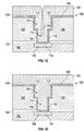
- FIGS. 1A-1E illustrate a method of forming a cobalt interconnect with a Mn based adhesion layer and a cobalt-containing fill layer according to an illustrative example.
- FIG. 1A illustrates a substrate 106 with top surface 118 that may be used as a substrate on which a cobalt interconnect can be formed.
- Substrate 106 can include any portion of a partially fabricated IC on which a cobalt interconnect is ultimately fabricated.
- substrate 106 will typically include, or have formed thereon, active and passive devices.
- a conductive region 150 is included in substrate 106, on to which a cobalt interconnect is ultimately formed.
- the substrate 106 has been processed through front end of line (FEOL), and the conductive region 150 is a diffusion region formed in a crystalline semiconductor substrate or layer (e.g., the conductive region is a source or drain region of a transistor).
- the conductive region 150 is an underlying metal line in a back end of line (BEOL) metallization structure, as is described in greater detail below in association with FIG. 2 .
- BEOL back end of line
- 150 is not intended to indicate that 150 is necessarily nonmonolithic with 106 or was formed with a different process or non-simultaneously with 106.
- area 150 may also be an area doped differently than the rest of 106 when 150 is to serve as a source or drain.
- embodiments may be ideally suited for fabricating semiconductor ICs such as, but not limited to, microprocessors, memories, charge-coupled devices (CCDs), system on chip (SoC) ICs, or baseband processors
- semiconductor ICs such as, but not limited to, microprocessors, memories, charge-coupled devices (CCDs), system on chip (SoC) ICs, or baseband processors
- CCDs charge-coupled devices
- SoC system on chip
- the disclosed methods and structures may also be used to fabricate individual semiconductor devices (e.g., a cobalt structure described herein may be used to fabricate a gate electrode of a metal oxide semiconductor (MOS) transistor).
- MOS metal oxide semiconductor
- a dielectric layer 102 is formed above substrate 106.
- the dielectric layer 102 may be composed of any suitable dielectric or insulating material such as, but not limited to, silicon dioxide, SiOF, carbon-doped oxide, a glass or polymer material, and the like.
- An opening is formed in the dielectric layer. The opening exposes the conductive region 150 to which contact (indirect or direct) by a cobalt interconnect is ultimately made. In one example, as depicted in FIG.
- the opening includes a lower opening 114 (e.g., a via hole or slot) with sidewalls 116 and an upper opening 110 (e.g., a metal line trench) with sidewalls 112, as is common in a dual damascene process.
- a single opening may instead be formed in the dielectric layer 102 (e.g., as is used in a single damascene approach where only a line or a via, but not both, is fabricated in a single operation).
- the opening or openings may be fabricated in dielectric layer 102 by well known lithography and etch processing techniques typically used in damascene and dual damascene type fabrication.
- the dielectric layer 102 is formed on an etch stop layer 104 disposed on substrate 106.
- the etch stop layer 104 may be composed of a material such as silicon nitride or silicon oxynitride.
- a Mn based adhesion layer 120 (e.g., an adhesion layer including Mn, MnN, MnSi x N y and the like) is deposited.
- a seed layer may be formed on a TNT based adhesion layer.
- Seed layers such as the seed layer disclosed in U.S. Patent App. publication US2014183738 , may facilitate formation of fill material. However, no such seed layer is needed in the embodiment of FIG. 1B . Nor is deposition of an alloy between an adhesion layer and a seed layer needed in the embodiment of FIG. 1B .
- a Mn based adhesion layer may directly contact ILD 102 and directly contact cobalt fill (described below) without the need for a TNT based adhesion layer, any seed layer, or any alloy layer between a TNT based adhesion layer and a seed layer.
- the Mn based adhesion layer 120 may be formed on a top surface 108 of the dielectric layer 102 as well as on the exposed top surface 118 of the substrate 106 (e.g., on conductive region 150). While 106 is referred to as "substrate”, 106 could be a metal interconnect line, and the like.
- the Mn based adhesion layer 120 is also formed on the sidewalls 116 of the upper opening 114, and the sidewalls 112 of the lower opening 110.
- Mn based adhesion layer 120 may be a conformal layer composed of a material including Mn, MnN, MnSi x N y , MnSi x O y (e.g., Mn 2 [SiO 4 ], MnSiO 3 ), other Mn based silicates, and the like.
- the Mn content may include 90-100% Mn, where contamination (i.e., the remaining 10%) may include C, H, O and combinations thereof.
- the adhesion layer including MnN x the Mn may compose 0-50% Mn and the N may compose 0-50%.
- the adhesion layer may include Mn 4 N or Mn 3 N 2 .
- the Mn and N may include up to 50% with the Si constituting the remainder of the material.
- Mn, N, and Si may be included with one another in various adhesion multilayer combinations such as bilayers or trilayers (e.g., an adhesion layer includes one sublayer including MnN and another sublayer including Mn), (e.g., one adhesion layer including a sublayer having Mn and N and another sublayer including primarily Mn), (e.g., one adhesion layer including a sublayer including MnN x Si y and another sublayer including primarily Mn), and the like.
- % of composition refers to atomic %.
- the Mn based adhesion layer 120 is formed to a thickness less than 3 nm, and typically 1 nm to 3 nm. In an embodiment thickness ranges for layer 120 (whether layer 120 includes a single layer or multiple sublayers such as one sublayer including MnN and another immediately adjacent sublayer including Mn) may range from 0.1A to 50A. In an example, layer 120 is between 10A-20A including, for example, 10, 12, 14, 16, 18, or 20A.
- conductive region 150 includes at least some germanium (e.g., an exposed doped silicon germanium or doped germanium region, or a metal germanide region). In an example, conductive region 150 includes at least some silicon (e.g., an exposed doped silicon region, or a metal silicide region).
- the layer 120 may be deposited or grown by chemical vapor deposition (CVD), atomic layer deposition (ALD), physical vapor deposition (PVD), electroplating, electroless plating or other suitable process that deposits conformal thin films.
- the layer 120 is deposited to form a high quality conformal layer that sufficiently and evenly covers all exposed surfaces within the openings and top surfaces.
- the adhesion layer may be formed, in one example, by depositing the Mn based material at a slow deposition rate to evenly and consistently deposit the conformal adhesion layer.
- compatibility of a subsequently formed fill material such as cobalt
- the layer 120 can assist a deposition process by providing appropriate surface energetics for deposition thereon.
- Deposition recipes of thin films using processes such as CVD, ALD, and PVD may vary depending on the desired process time, thickness, and quality of conformity. For example, utilizing CVD to deposit the adhesion layer 120 may create a conformal thin film layer more quickly than it would take an ALD process to deposit the same layer; however, the quality of the thin film deposited by the CVD process may be lower than the quality of the thin film deposited by the ALD process.
- the layer 120 is deposited by a PVD process. The PVD process may be performed with an increased distance between the receiving substrate and the corresponding sputter target to form a highly conformal thin film.
- a fill material 122 may be formed on the exposed surfaces of the adhesion layer 120, such that the fill material 122 completely fills the openings 110 and 114 and is formed on the top surface of the adhesion layer 120 and on the top surface 108 of dielectric 102.
- a seam 124 may be formed within the openings 110, 114 during deposition of the fill material 122.
- the fill material 122 is composed of a dilute alloy composed of approximately 0.25-5% of a non-cobalt element (e.g., Al, Ni, Cu, Ag, Au, Mn, Ti, V, Cr, Fe, Ta, W, Ru, P, B, C, N, Si, Ge, Mg, Zn, Rh, Pt, Cd, Hf, In, Sn, C, O, Be, Ca, Zr, Nb, Mo, Ir, Re, or Pd) with the remainder approximately 95+% cobalt.
- a dilute alloy can involve, either during deposition or processing subsequent to deposition, migration of the non-cobalt species to surfaces of fill 122.
- the migration can provide a diffusion barrier for the cobalt (in addition to adhesion/barrier layer 120) and/or be used to enhance adhesion of the cobalt to layer 120. Grain boundaries within the cobalt may also be filled by the non-cobalt species.
- the fill material 122 consists essentially only of cobalt.
- the fill material 122 is at least 90% cobalt.
- the fill material 122 is composed of at least 50% cobalt.
- the cobalt fill material 122 may be formed by a process such as, but not limited to, CVD, ALD, PVD, electroplating, or electroless plating.
- the process method used to form the fill material 122 may be different than the process used to form the layer 120.
- the layer 120 may be formed conformally, while the fill material 122 is formed in a non-conformal or bottom up approach.
- the layer 120 may be formed by an ALD deposition process that forms a conformal layer on exposed surfaces of the receiving substrate, while the fill material 122 may be formed by PVD process that directionally sputters the fill material onto the surfaces of the layer 120, with greater deposition rates on flat horizontal surfaces as opposed to on more vertically oriented sidewall surfaces.
- the layer 120 may be formed by an ALD deposition process that forms a conformal layer on exposed surfaces of the receiving substrate, while the fill material 122 may be formed by an electroplating process that grows the fill material from the surfaces of the layer 120.
- the layer 120 may be formed by a CVD deposition process and the fill material may be formed by a PVD process.
- the layer 120 and the fill material 122 may be deposited by the same process (e.g. ALD, CVD, or PVD) but with different sets of deposition parameters, such as pressure, deposition rate, temperature, and the like.
- the layer 120 and the fill material 122 may be deposited by a CVD process; however, the set of parameters used in the CVD processing for the adhesion layer 120, such as deposition pressure and temperature, may be different than the set of parameters used in the CVD processing for the fill material 122.
- the layer 120 and the fill material 122 are formed by a PVD process, but the layer 120 may be formed by a PVD process with a larger distance between the target and the receiving substrate than the PVD process used to form the fill material 122.
- the metal fill material 122 is formed by a colummated PVD process, while the layer 120 is formed by a non-colummated PVD process.
- the layer 120 is formed by an ALD process with a lower deposition rate than the deposition rate of the ALD process used to form the fill material 122 such that the layer 120 is formed more conformally than the fill material 122.
- an anneal process may optionally be performed to reflow the deposited interconnect layer.
- the seam 124 from FIG. 1C may be removed subsequent to the anneal process, forming a solid structure within openings 110 and 114 within dielectric layer 102.
- the anneal process may help grow larger grain structures within the fill material 122, decreasing resistivity and expelling impurities from poor grain structures.
- the anneal process uses gasses such as nitrogen, hydrogen, and argon.
- the anneal process may be performed at a temperature less than the thermal budget of the backend structures. For example, the anneal process is performed at a temperature of room temperature to 300°C, 400°C, 500°C or more.
- the anneal process is performed at a temperature that is higher than the melting point of fill material 122 but lower than the thermal budget of the backend structures.
- the anneal process can vary widely (e.g., room temperature to 300°C, 400°C, 500°C or more for interconnects ranging up to 900°C for Front end applications).
- the anneal temperature is not higher than the melting point of the material being annealed as reflow of materials to be annealed can happen at much lower temperatures than the melting point for the material to be annealed.
- anneal temperatures for the material to be annealed may be less than the thermal budget of backend structures.
- a cycling technique may optionally be utilized to deposit the interconnect layer 122 (also referred to as fill layer 122) within the openings 114 and 110 without the seam 124.
- One cycle may involve one deposition of the fill material 122 and one anneal process.
- the anneal operation of one cycle may be set at a temperature and time duration to briefly reflow the fill material to improve step coverage.
- the deposition operation of one cycle may be a short deposition to deposit less fill material, such that several operations are required to completely fill the via and line openings 114 and 110. In one embodiment, less than 5 cycles are needed to deposit the fill material 122 without a seam 124.
- a chemical mechanical planarization (CMP) process may be performed to remove the fill material 122 and the adhesion layer 120 disposed above the top surface 108 of the dielectric layer 102.
- the CMP process may be a timed CMP process that is timed to stop at the top surface 108 of the line dielectric layer.
- the CMP process may utilize the top surface 108 of the line dielectric layer as a stopping layer. Because the thickness of the fill material deposited above the top surface of the line dielectric layer may vary, utilizing the top surface 108 as a stopping layer may be a more reliable method.
- an etch process is used to remove the fill material 122 and the layer 120 disposed above the top surface 108 of the dielectric layer 102.
- FIG. 2 illustrates a cross-section 200 of a portion of an IC structure with cobalt metal interconnects according to an illustrative example.
- a stack of dielectric layers 102 includes metal interconnects having adhesion layers 120 and metal (e.g., cobalt) fill layers 124.
- the portion of the IC structure shown in Figure 2 can be a portion of a back end of line (BEOL) metallization structure as found, for example, in a microprocessor die or memory die.
- BEOL back end of line
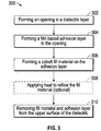
- FIG. 3 is a flow chart 300 illustrating a method of forming a cobalt metal interconnect according to an embodiment of the present invention.
- an opening is formed in a dielectric layer to expose a conductive region in a substrate (or on an additional metal interconnect).
- a Mn based adhesion/barrier layer is formed over the substrate, in contact with the conductive region, as well as over the dielectric layer and on sidewalls of the opening.
- a fill material is formed on the adhesion layer and fills the opening.
- the fill material is composed of a cobalt-based material.
- heat is applied to reflow the fill material.
- the fill material and adhesion layer material disposed above an upper surface of the dielectric layer are removed.
- a cobalt-based plug is formed in a lower portion (e.g., a via hole or slot) of an opening in a dielectric layer.
- a cobalt-based conductive line is then formed on the cobalt-based plug, in an upper portion (e.g., a metal line trench) of the opening, to form a cobalt interconnect.
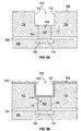
- FIGS. 4A-4D illustrate a method of forming a cobalt metal interconnect according to an embodiment of the invention. The method begins with the same structure as illustrated and described in association with FIG. 1B , which includes adhesion layer 120 and will not be described again for the sake of brevity.
- a plug 420 is formed on adhesion layer 120.
- the plug 420 is formed only within the lower opening 114 of the dielectric layer 102 such that the lower opening 114 is completely filled with plug material 420.
- the top surface of the plug 420 may not be planar with the top surface of the lower opening 114.
- the top surface of the plug 420 may be higher or lower than the top surface of the lower opening.
- the top surface of the plug 420 may be at, above, or below the horizontal top surface of layer 120 where layer 120 is horizontally disposed at the top of 114 and bottom of 110.
- the plug 420 has a top surface just below the horizontal top surface of layer 120 where layer 120 is horizontally disposed at the top of 114 and bottom of 110.
- the top surface of the plug 420 may form a mushroom-like dome as a result of the growth profile during formation of plug 420.
- plug 420 is formed in a bottom-up approach. That is, the plug 420 is not formed by conformal deposition.
- the formation of plug 420 is performed by selectively depositing on, and then growing from, the surface of layer 120 directly above the conductive region 150.
- the plug 420 is formed by electrolessly plating the plug material onto an exposed and compatible surface of layer 120.
- the conductive region 150 has an upper metalized or metal-containing surface such as cobalt (Co), copper (Cu) or Tungsten (W), and a cobalt-based plug 420 is formed by electroless deposition involving bottom-up growth from the layer 120 above the metalized or metal-containing surface of conductive region 150.
- other suitable bottom-up fill and growth deposition approaches may be used such as, but not limited to, electroplating.
- a bottom-up fill approach is one in which a deposition rate is faster on planar or flat surfaces than on vertical sidewall surfaces.
- the plug 420 may be a cobalt-based plug composed of at least 50% cobalt.
- the plug 420 is composed of at least 90% cobalt.
- the non-cobalt remainder of the plug 420 composition can include one or more of Al, Ni, Cu, Ag, Au, Mn, Ti, V, Cr, Fe, Ta, W, Ru, P, B, C, N, Si, Ge, Mg, Zn, Rh, Pt, Cd, Hf, In, Sn, C, O, Be, Ca, Zr, Nb, Mo, Ir, Re, or Pd.
- the plug 420 is composed of a cobalt-based compound or alloy material.
- the plug 420 is composed of a dilute alloy composed of approximately 0.25-5% of a non-cobalt element, such as those listed above, with the remainder approximately 95+% cobalt, is used.
- a dilute alloy can involve, either during deposition or processing subsequent to deposition, migration of the non-cobalt species to surfaces or interfaces of the cobalt plug. The migration can provide a diffusion barrier for the cobalt and/or be used to enhance adhesion of the cobalt to layer 120. Grain boundaries within the cobalt may also be filled by the non-cobalt species.
- the plug 420 may include less than 50% cobalt, but still be referred to as a cobalt-based material.
- Exemplary embodiments of cobalt-based compound plug 420 materials include cobalt silicide or cobalt germanide plug materials.
- conductive region 150 includes at least some germanium (e.g., an exposed doped silicon germanium or doped germanium region, or a metal germanide region), and the plug 420 material is a cobalt germanide layer.
- conductive region 150 includes at least some silicon (e.g., an exposed doped silicon region, or a metal silicide region), and the plug 420 material is a cobalt silicide layer.
- cobalt-based alloy plug 420 materials include cobalt alloyed with one or more of the following: Al, Ni, Cu, Ag, Au, Mn, Ti, V, Cr, Fe, Ta, W, Ru, P, B, C, N, Si, Ge, Mg, Zn, Rh, Pt, Cd, Hf, In, Sn, C, O, Be, Ca, Zr, Nb, Mo, Ir, Re, or Pd.
- the cobalt plug 420 may have a small grain structure.
- the above mentioned dopant i.e., the 0.25-5% of a non-cobalt element
- the dopant could be used without layer 120 so that cobalt would adhere directly to sidewall 116 as well as portion 150.
- the dopant essentially creates a layer 120 (an adhesion layer) by diffusion to interfaces such as interfaces at 150 and 116.
- the dopant forms a layer with portion 150.
- the dopant makes no layer formation with 150 so that the barrier is bottomless and plug 420 directly contacts area 150.
- pretreatment 422 may optionally be performed on the exposed top surface of the plug 420 and layer 120.
- Pretreatment may be performed by a plasma process or ion bombardment to enhance adhesion of a later formed compound to the treated surface.
- pretreatment may be performed in a plasma chamber at a temperature ranging from room temperature up to approximately 300°C, 400°C, 500°C or more for approximately 20 to 60 seconds utilizing, for example, H 2 /He plasma, Ar plasma, NH 3 plasma, N 2 plasma, and/or combinations thereof.
- the pretreatment may include Ar ion bombardment. It is to be understood that such pretreatment may be performed at other stages of the process flow (e.g., prior to forming plug materials).
- the pretreatment is performed before layer 120 is formed.
- a treatment of layer 120 can be quite beneficial to density without affecting dielectrics such as layer 102.
- a fill material 424 is formed on the plug 420 and layer 120 within upper opening 110.
- a seam 426 may be formed within the upper opening 110 subsequent to deposition of the fill material 424.
- fill material 424 is composed of a material comprising cobalt.
- fill material may be composed of, and deposited by, materials and processes described above for fill material 122.
- the fill material 424 differs from the plug 420 material by composition and may also differ by deposition technique.
- An anneal process may optionally be performed to reflow the deposited fill material 424.
- the seam 426 from FIG. 4C may be removed subsequent to the anneal process, forming a solid structure within openings 110 and 114 within dielectric layer 102.
- the anneal process may enable growth of larger grain structures within the fill material 424, decreasing resistivity and expelling impurities from otherwise poor grain structures.
- the anneal process involves use of a forming gas such as, but not limited to, nitrogen, hydrogen, or argon.
- the anneal process may be performed at a temperature less than the thermal budget of the backend structures. For example, in one embodiment, the anneal process is performed at a temperature of room temperature to 300°C, 400°C, 500°C or more.
- the anneal process is performed at a temperature that is higher than the melting point of fill material 424 but lower than the thermal budget of the backend structures.
- the anneal temperature is not higher than the melting point of the material being annealed as reflow of materials to be annealed can happen at much lower temperatures than the melting point for the material to be annealed. In such embodiments anneal temperatures for the material to be annealed may be less than the thermal budget of backend structures.
- a cycling technique is optionally utilized to deposit the fill material 424 within the opening 110 without the seam 426.
- One cycle may involve a single deposition of the fill material 424 and a single anneal process.
- the anneal operation of one cycle may be set at a temperature and time duration to briefly reflow the fill material 424 to improve step coverage.
- the deposition operation of one cycle may be a short deposition to deposit less fill material 424, such that several operations are required to completely fill the upper opening 110. In one embodiment, less than 5 cycles are needed to deposit the fill material 424 without a seam 426.
- a CMP process may be performed to remove the fill material 424 above the top surface of layer 120 to provide the cobalt-based structure 428.
- the CMP process may be a timed CMP process that is timed to stop at the top surface 108 of the line dielectric layer.
- the CMP process may utilize the top surface 108 of the dielectric layer 102 as a stopping layer. Because the thickness of the fill material deposited above the top surface 108 of the dielectric layer 102 may vary, utilizing the top surface 108 as a stopping layer may be a more reliable method.
- an etch process is used to remove the fill material 424 above the top surface 108 of the dielectric layer 102.
- a cobalt-based plug is formed in a lower portion (e.g., a via hole or slot) of an opening in a dielectric layer.
- An adhesive layer is then formed in an upper portion (e.g., a metal line trench) of the opening, over the cobalt-based plug.
- a cobalt-based conductive line is then formed on the portion of the adhesive layer that is directly over the plug to fill the upper portion of the opening to form a cobalt interconnect.
- FIGS. 5A-5D illustrate a method of forming a cobalt interconnect with a Mn based adhesion layer and a cobalt containing fill layer according to an embodiment of the invention.
- the method begins with the same structure as illustrated and described in association with FIG. 1A .
- the cobalt-based plug 420 is formed in the lower opening 114 of the dielectric layer 102, on the conductive region 150 of substrate 106.
- the adhesion layer be first formed along the side walls of dielectric 102 and/or on top of portion 150 before plug 420 is formed.
- a Mn based adhesion layer 524 (e.g., Mn, MnN, MnSi x N y MnSi x O y (e.g., Mn 2 [SiO 4 ], MnSiO 3 ), other Mn based silicates, and the like) is deposited conformally with the structure of FIG. 5A .
- the Mn based adhesion layer 524 is formed in the upper opening 114 of the dielectric layer 102 and on the exposed plug 420.
- the composition and method of forming the adhesion layer 524 may be as described for adhesion layer 120 of FIG. 1B .
- a fill material 526 is formed on the adhesion layer 524, within upper opening 110, and on the top surface 108 of the dielectric layer 102.
- a seam 528 may be formed within the opening 110 subsequent to deposition of the fill material 526.
- the composition and method of forming the fill material layer 526 may be as described for fill material 122 of FIG. 1C .
- the plug 420 and the fill material 526 are all cobalt-based, they differ from one another by composition and may also differ by deposition technique.
- An anneal process may optionally be performed to reflow the deposited fill material 526.
- the seam 528 from FIG. 5C may be removed subsequent to the anneal process, forming a solid structure within opening 110 of dielectric layer 102.
- the anneal process may enable growth of larger grain structures within the fill material 526, decreasing resistivity and expelling impurities from poor grain structures.
- the anneal process involves a use of gas such as, but not limited to, nitrogen, hydrogen, or argon.
- the anneal process may be performed at a temperature less than the thermal budget of the backend structures. For example, in one embodiment, the anneal process is performed at a temperature of room temperature to 300°C, 400°C, 500°C or more..
- the anneal process is performed at a temperature that is higher than the melting point of fill material 526 but lower than the thermal budget of the backend structures.
- the anneal temperature is not higher than the melting point of the material being annealed as reflow of materials to be annealed can happen at much lower temperatures than the melting point for the material to be annealed. In such embodiments anneal temperatures for the material to be annealed may be less than the thermal budget of backend structures.
- a cycling technique may be utilized to deposit the fill material 526 within the opening 110 without the seam 528.
- One cycle may involve one deposition of the fill material 526 and one anneal process.
- the anneal operation of one cycle may be set at a temperature and time duration to briefly reflow the fill material to improve step coverage.
- the deposition operation of one cycle may be a short deposition to deposit less fill material, such that several operations are required to completely fill the opening 510. In one embodiment, less than 5 cycles are needed to deposit the fill material 526 without a seam 528.
- a CMP process may be performed to remove the fill material 526 and the adhesion layer 524 disposed above the top surface 108 of the dielectric layer 102 to provide the cobalt-based structure 530.
- the CMP process may be a timed CMP process that is timed to stop at the top surface 108 of the dielectric layer 102.
- the CMP process may utilize the top surface 108 of the dielectric layer 102 as a stopping layer. Because the thickness of the fill material deposited above the top surface 108 of the dielectric layer 102 may vary, utilizing the top surface 108 as a stopping layer may be a more reliable method.
- an etch process is used to remove the fill material 526 and the layer 524 disposed above the top surface 108 of the dielectric layer 102.
- FIG. 6 is a flow chart 600 illustrating a method of forming a cobalt metal interconnect according to an embodiment of the present invention.
- an opening is formed in a dielectric layer to expose a conductive region in a substrate.
- a cobalt plug is formed in a lower portion of the opening, in contact with the conductive region.
- a Mn based adhesion layer e.g., Mn, MnN, MnSi x N y and the like
- a fill material is formed on the plug and adhesion layer to fill the opening.
- the fill material is composed of a cobalt-based material.
- heat is applied to reflow the fill material.
- the fill material disposed above an upper surface of the dielectric layer is removed.
- the fill material and the plug both include cobalt, but have different material compositions.
- the fill material and the plug both include cobalt, but are formed by different deposition or growth techniques.
- the fill material and the plug both include cobalt, but have different material compositions and are formed by different deposition or growth techniques.
- a metal gate electrode of a semiconductor device is composed, as least partially, of cobalt. That is, embodiments of the present invention need not be limited to forming cobalt-based interconnects.
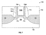
- Figure 7 depicts a metal oxide semiconductor field effect transistor (MOS-FET) 700 fabricated on a substrate 702, in accordance with an embodiment of the present invention.
- a gate dielectric layer 704 is disposed above a channel region 706, and a gate electrode 708 is disposed above gate dielectric layer 704.
- Gate dielectric layer 704 and gate electrode 708 may be isolated by gate isolation spacers 710.
- Tip extensions 712 may be formed by implanting dopant atoms into substrate 702.
- Source and drain regions e.g., strain-inducing source/drain regions 720
- tip extensions 712 may be formed simultaneously with the source and drain regions to create "epi" tip extensions.
- the channel region 706 is composed of a semiconductor material, such as single crystalline silicon.
- the gate electrode 708 is a metal gate electrode (e.g., the workfunction of the gate electrode 708 is based on a metal or metal-containing layer).
- the metal gate electrode is composed, at least somewhat, of cobalt.
- the metal gate electrode 708 includes a Mn based adhesion layer (e.g., Mn, MnN, MnSi x N y and the like as described above) 708A and a cobalt fill metal thereon 708B.
- the cobalt-based material or film 708B is composed of at least 90% cobalt.
- the cobalt-based material or film 708B is composed of a dilute alloy having approximately 0.25-5% of a non-cobalt element, with the remainder approximately 95+% cobalt.
- the MOS-FET 700 may be a planar device or include a three-dimensional body (e.g., as in a double-gate, fin-fet, tri-gate, or gate-all-around transistor).
- the substrate 702 may be a planar substrate or depict a cross-sectional view of a three-dimensional body.
- isolation layers e.g., interlayer dielectric layer 740, and metallization routing layers used for integrating MOS-FET 700 into, e.g., an integrated circuit may also be included, as is well known in the art.
- a mobile computing node such as a cellular phone, Smartphone, tablet, Ultrabook®, notebook, laptop, personal digital assistant, and mobile processor based platform
- the subject matter of Examples 17-19 can optionally include a dielectric layer formed directly on top of the adhesive layer and the fill material, the dielectric layer comprising manganese; wherein the fill material also includes manganese.
- the manganese may have migrated from the adhesion layer into the dielectric.
- terms designating relative vertical position refer to a situation where a device side (or active surface) of a substrate or integrated circuit is the "top” surface of that substrate; the substrate may actually be in any orientation so that a "top” side of a substrate may be lower than the “bottom” side in a standard terrestrial frame of reference and still fall within the meaning of the term “top.”
- the term “on” as used herein does not indicate that a first layer “on” a second layer is directly on and in immediate contact with the second layer unless such is specifically stated; there may be a third layer or other structure between the first layer and the second layer on the first layer.
- the embodiments of a device or article described herein can be manufactured, used, or shipped in a number of positions and orientations.
Landscapes
- Engineering & Computer Science (AREA)
- Microelectronics & Electronic Packaging (AREA)
- Power Engineering (AREA)
- Physics & Mathematics (AREA)
- Condensed Matter Physics & Semiconductors (AREA)
- General Physics & Mathematics (AREA)
- Computer Hardware Design (AREA)
- Manufacturing & Machinery (AREA)
- Chemical & Material Sciences (AREA)
- Ceramic Engineering (AREA)
- Composite Materials (AREA)
- Materials Engineering (AREA)
- Crystallography & Structural Chemistry (AREA)
- Internal Circuitry In Semiconductor Integrated Circuit Devices (AREA)
- Electrodes Of Semiconductors (AREA)
- Insulated Gate Type Field-Effect Transistor (AREA)
Claims (15)
- Structure d'interconnexion métallique, comprenant :une couche diélectrique (102) sur un substrat (106) ;une ouverture dans la couche diélectrique (102), l'ouverture ayant des parois latérales et exposant une région conductrice du substrat (106) et/ou d'une structure d'interconnexion supplémentaire ;une fiche (420), comprenant du cobalt, contenue dans la partie inférieure de l'ouverture ;une couche d'adhérence (120), comprenant du manganèse, sur la région conductrice et les parois latérales ;un matériau de remplissage (424), comprenant du cobalt, dans la partie supérieure de l'ouverture sur une surface de la couche d'adhérence et sur la fiche (420), la fiche (420) remplissant la partie inférieure de l'ouverture, et le matériau de remplissage (424) remplissant la partie supérieure de l'ouverture depuis une partie basse de la partie supérieure jusqu'à une partie haute de la partie supérieure, et la fiche (420) et le matériau de remplissage (424) étant formés à partir de compositions différentes.
- Structure de la revendication 1, dans laquelle le matériau de remplissage (424) est composé, pour au moins 50 % en atomes, de cobalt.
- Structure de la revendication 2, dans laquelle la couche d'adhérence (120) comporte au moins un élément choisi dans le groupe constitué par le silicium, l'azote, le carbone, l'hydrogène, et l'oxygène.
- Structure de la revendication 2, dans laquelle l'épaisseur de la couche d'adhérence (120) ne dépasse pas 50 A.
- Structure de la revendication 4, dans laquelle la couche d'adhérence (120) est en contact direct avec le matériau de remplissage (424).
- Structure de la revendication 5, dans laquelle la couche d'adhérence (120) est en contact direct avec la région conductrice.
- Structure de la revendication 6, dans laquelle la couche d'adhérence (120) est en contact direct avec la couche diélectrique (102).
- Structure de la revendication 7, dans laquelle le matériau de remplissage (424) comporte du manganèse qui est en contact direct avec le manganèse contenu dans la couche d'adhérence (120).
- Structure de la revendication 2, dans laquelle le matériau de remplissage (424) comporte au moins un élément choisi dans un groupe constitué par le silicium et le manganèse.
- Structure de la revendication 2, dans laquelle (a) la couche d'adhérence (120) comporte une première partie en contact direct avec la couche diélectrique (102) et une deuxième partie en contact direct avec la région conductrice, et (b) la première partie comporte un plus fort pourcentage atomique de manganèse que la deuxième partie.
- Structure de la revendication 10 dans laquelle la couche d'adhérence (120) ne sépare pas complètement la région conductrice du matériau de remplissage (424) et le matériau de remplissage (424) est en contact direct avec une partie de la région conductrice.
- Structure de la revendication 1 comprenant une couche diélectrique (102) formée juste au-dessus de la couche d'adhérence (120) et du matériau de remplissage (424), la couche diélectrique (102) comprenant du manganèse, le matériau de remplissage (424) comportant également du manganèse.
- Structure de la revendication 1 comprenant une couche diélectrique (102) formée juste au-dessus du matériau de remplissage (424), la couche diélectrique (102) comprenant un premier matériau, le premier matériau étant également contenu dans le matériau de remplissage (424) et le premier matériau étant choisi dans le groupe comprenant Al, Ni, Cu, Ag, Au, Mn, Ti, V, Cr, Fe, Ta, W, Ru, P, B, C, N, Si, Ge, Mg, Zn, Rh, Pt, Cd, Hf, In, Sn, C, O, Be, Ca, Zr, Nb, Mo, Ir, Re, et Pd.
- Procédé de formation d'une structure d'interconnexion métallique, comprenant :la formation d'une ouverture dans une couche diélectrique (102) sur un substrat (106), l'ouverture exposant une région conductrice du substrat (106) et/ou d'une structure d'interconnexion supplémentaire ;la formation d'une fiche (420), comprenant du cobalt, contenue dans la partie inférieure de l'ouverture ;la formation d'une couche d'adhérence (120), comprenant du manganèse, dans l'ouverture et sur la région conductrice et également sur les parois latérales ;la formation d'un matériau de remplissage (424), comprenant du cobalt, dans la partie supérieure de l'ouverture sur une surface de la couche d'adhérence (120) et sur la fiche (420), la fiche (420) remplissant la partie inférieure de l'ouverture, et le matériau de remplissage (424) remplissant la partie supérieure de l'ouverture depuis une partie basse de la partie supérieure jusqu'à une partie haute de la partie supérieure, et la fiche (420) et le matériau de remplissage (424) étant formés à partir de compositions différentes ; etle retrait de parties du matériau de remplissage (424) et de la couche d'adhérence (120) au-dessus d'une surface supérieure de la couche diélectrique (102).
- Procédé de la revendication 14 comprenant la formation de la couche d'adhérence (120) avec un procédé conforme et la formation de la couche de remplissage avec un procédé non conforme.
Priority Applications (1)
| Application Number | Priority Date | Filing Date | Title |
|---|---|---|---|
| EP21170662.7A EP3907755A3 (fr) | 2013-12-20 | 2015-02-21 | Interconnexions à base de cobalt et leurs procédés de fabrication |
Applications Claiming Priority (2)
| Application Number | Priority Date | Filing Date | Title |
|---|---|---|---|
| US14/137,526 US9997457B2 (en) | 2013-12-20 | 2013-12-20 | Cobalt based interconnects and methods of fabrication thereof |
| PCT/IB2015/000198 WO2015092780A1 (fr) | 2013-12-20 | 2015-02-21 | Interconnexions à base de cobalt et procédés pour leur fabrication |
Related Child Applications (1)
| Application Number | Title | Priority Date | Filing Date |
|---|---|---|---|
| EP21170662.7A Division EP3907755A3 (fr) | 2013-12-20 | 2015-02-21 | Interconnexions à base de cobalt et leurs procédés de fabrication |
Publications (3)
| Publication Number | Publication Date |
|---|---|
| EP3084810A1 EP3084810A1 (fr) | 2016-10-26 |
| EP3084810A4 EP3084810A4 (fr) | 2017-09-06 |
| EP3084810B1 true EP3084810B1 (fr) | 2021-04-28 |
Family
ID=53400881
Family Applications (2)
| Application Number | Title | Priority Date | Filing Date |
|---|---|---|---|
| EP15729733.4A Active EP3084810B1 (fr) | 2013-12-20 | 2015-02-21 | Interconnexions à base de cobalt et procédés pour leur fabrication |
| EP21170662.7A Pending EP3907755A3 (fr) | 2013-12-20 | 2015-02-21 | Interconnexions à base de cobalt et leurs procédés de fabrication |
Family Applications After (1)
| Application Number | Title | Priority Date | Filing Date |
|---|---|---|---|
| EP21170662.7A Pending EP3907755A3 (fr) | 2013-12-20 | 2015-02-21 | Interconnexions à base de cobalt et leurs procédés de fabrication |
Country Status (7)
| Country | Link |
|---|---|
| US (5) | US9997457B2 (fr) |
| EP (2) | EP3084810B1 (fr) |
| JP (1) | JP6652245B2 (fr) |
| KR (3) | KR20230054492A (fr) |
| CN (2) | CN114361132A (fr) |
| TW (1) | TWI610398B (fr) |
| WO (1) | WO2015092780A1 (fr) |
Families Citing this family (45)
| Publication number | Priority date | Publication date | Assignee | Title |
|---|---|---|---|---|
| US9997457B2 (en) * | 2013-12-20 | 2018-06-12 | Intel Corporation | Cobalt based interconnects and methods of fabrication thereof |
| US9847289B2 (en) * | 2014-05-30 | 2017-12-19 | Applied Materials, Inc. | Protective via cap for improved interconnect performance |
| EP3155650A4 (fr) * | 2014-06-16 | 2018-03-14 | Intel Corporation | Élimination de lignes de soudure d'interconnexions métalliques |
| US9601430B2 (en) * | 2014-10-02 | 2017-03-21 | Taiwan Semiconductor Manufacturing Co., Ltd. | Semiconductor device structure and method for forming the same |
| US20160276156A1 (en) * | 2015-03-16 | 2016-09-22 | Taiwan Semiconductor Manufacturing Company Ltd. | Semiconductor device and manufacturing process thereof |
| US9722038B2 (en) * | 2015-09-11 | 2017-08-01 | International Business Machines Corporation | Metal cap protection layer for gate and contact metallization |
| US9484255B1 (en) * | 2015-11-03 | 2016-11-01 | International Business Machines Corporation | Hybrid source and drain contact formation using metal liner and metal insulator semiconductor contacts |
| US9741577B2 (en) | 2015-12-02 | 2017-08-22 | International Business Machines Corporation | Metal reflow for middle of line contacts |
| TWI637899B (zh) * | 2015-12-15 | 2018-10-11 | 村田製作所股份有限公司 | 微機電裝置和製造其之方法 |
| US10446496B2 (en) | 2016-02-17 | 2019-10-15 | International Business Machines Corporation | Self-forming barrier for cobalt interconnects |
| US9837350B2 (en) * | 2016-04-12 | 2017-12-05 | International Business Machines Corporation | Semiconductor interconnect structure with double conductors |
| US10438849B2 (en) * | 2016-04-25 | 2019-10-08 | Applied Materials, Inc. | Microwave anneal to improve CVD metal gap-fill and throughput |
| US10438847B2 (en) * | 2016-05-13 | 2019-10-08 | Lam Research Corporation | Manganese barrier and adhesion layers for cobalt |
| US9799555B1 (en) * | 2016-06-07 | 2017-10-24 | Globalfoundries Inc. | Cobalt interconnects covered by a metal cap |
| US10049927B2 (en) * | 2016-06-10 | 2018-08-14 | Applied Materials, Inc. | Seam-healing method upon supra-atmospheric process in diffusion promoting ambient |
| US10079208B2 (en) | 2016-07-28 | 2018-09-18 | Globalfoundries Inc. | IC structure with interface liner and methods of forming same |
| US9953864B2 (en) | 2016-08-30 | 2018-04-24 | International Business Machines Corporation | Interconnect structure |
| US10049974B2 (en) * | 2016-08-30 | 2018-08-14 | International Business Machines Corporation | Metal silicate spacers for fully aligned vias |
| JP6559107B2 (ja) * | 2016-09-09 | 2019-08-14 | 東京エレクトロン株式会社 | 成膜方法および成膜システム |
| US9899317B1 (en) | 2016-09-29 | 2018-02-20 | International Business Machines Corporation | Nitridization for semiconductor structures |
| US9741609B1 (en) | 2016-11-01 | 2017-08-22 | International Business Machines Corporation | Middle of line cobalt interconnection |
| US10128151B2 (en) * | 2016-12-16 | 2018-11-13 | Globalfoundries Inc. | Devices and methods of cobalt fill metallization |
| DE112016007569T5 (de) * | 2016-12-30 | 2019-11-28 | Intel Corporation | Selbstjustierte hartmasken mit umgewandelten linern |
| US10177030B2 (en) * | 2017-01-11 | 2019-01-08 | International Business Machines Corporation | Cobalt contact and interconnect structures |
| US9805972B1 (en) * | 2017-02-20 | 2017-10-31 | Globalfoundries Inc. | Skip via structures |
| KR102292645B1 (ko) * | 2017-03-09 | 2021-08-24 | 삼성전자주식회사 | 집적회로 소자 |
| US10109490B1 (en) * | 2017-06-20 | 2018-10-23 | Globalfoundries Inc. | Cobalt interconnects formed by selective bottom-up fill |
| US10553481B2 (en) * | 2017-08-31 | 2020-02-04 | Taiwan Semiconductor Manufacturing Co., Ltd. | Vias for cobalt-based interconnects and methods of fabrication thereof |
| US20190096820A1 (en) * | 2017-09-28 | 2019-03-28 | Taiwan Semiconductor Manufacturing Co., Ltd. | Hardened interlayer dielectric layer |
| US11348828B2 (en) * | 2017-11-23 | 2022-05-31 | Taiwan Semiconductor Manufacturing Co., Ltd. | Interconnect structure and method of forming the same |
| US10541199B2 (en) | 2017-11-29 | 2020-01-21 | International Business Machines Corporation | BEOL integration with advanced interconnects |
| US10847413B2 (en) | 2017-11-30 | 2020-11-24 | Taiwan Semiconductor Manufacturing Company, Ltd. | Method of forming contact plugs for semiconductor device |
| US10340183B1 (en) * | 2018-01-02 | 2019-07-02 | Globalfoundries Inc. | Cobalt plated via integration scheme |
| US20190363048A1 (en) * | 2018-05-22 | 2019-11-28 | Lam Research Corporation | Via prefill in a fully aligned via |
| US10971398B2 (en) * | 2018-10-26 | 2021-04-06 | International Business Machines Corporation | Cobalt interconnect structure including noble metal layer |
| CN111261574A (zh) * | 2018-12-03 | 2020-06-09 | 长鑫存储技术有限公司 | 一种半导体结构及其制作方法 |
| FR3092589A1 (fr) * | 2019-02-08 | 2020-08-14 | Aveni | Electrodéposition d’un alliage de cobalt et utilisation en microélectronique |
| WO2020161256A1 (fr) | 2019-02-08 | 2020-08-13 | Aveni | Électrodéposition d'un alliage de cobalt ou de cuivre et son utilisation en microélectronique |
| US10818589B2 (en) | 2019-03-13 | 2020-10-27 | International Business Machines Corporation | Metal interconnect structures with self-forming sidewall barrier layer |
| US11292938B2 (en) | 2019-09-11 | 2022-04-05 | Rohm And Haas Electronic Materials Cmp Holdings, Inc. | Method of selective chemical mechanical polishing cobalt, zirconium oxide, poly-silicon and silicon dioxide films |
| US11189589B2 (en) * | 2019-09-25 | 2021-11-30 | Taiwan Semiconductor Manufacturing Company Ltd. | Semiconductor structure with raised implanted region and manufacturing method thereof |
| US11152257B2 (en) * | 2020-01-16 | 2021-10-19 | International Business Machines Corporation | Barrier-less prefilled via formation |
| US11581258B2 (en) | 2021-01-13 | 2023-02-14 | Nanya Technology Corporation | Semiconductor device structure with manganese-containing interconnect structure and method for forming the same |
| WO2022170169A1 (fr) | 2021-02-08 | 2022-08-11 | Macdermid Enthone Inc. | Procédé et compositions chimiques humides pour formation de barrière de diffusion |
| US20240063285A1 (en) * | 2022-08-22 | 2024-02-22 | Nanya Technology Corporation | Semiconductor device with assistant cap and method for fabricating the same |
Family Cites Families (38)
| Publication number | Priority date | Publication date | Assignee | Title |
|---|---|---|---|---|
| US20020019127A1 (en) * | 1997-02-14 | 2002-02-14 | Micron Technology, Inc. | Interconnect structure and method of making |
| EP1627098A1 (fr) * | 2003-05-09 | 2006-02-22 | Basf Aktiengesellschaft | Compositions servant au depot sans courant de materiaux ternaires pour l'industrie des semi-conducteurs |
| US7304388B2 (en) | 2003-06-26 | 2007-12-04 | Intel Corporation | Method and apparatus for an improved air gap interconnect structure |
| US7972970B2 (en) * | 2003-10-20 | 2011-07-05 | Novellus Systems, Inc. | Fabrication of semiconductor interconnect structure |
| US6967131B2 (en) * | 2003-10-29 | 2005-11-22 | International Business Machines Corp. | Field effect transistor with electroplated metal gate |
| JP5096669B2 (ja) * | 2005-07-06 | 2012-12-12 | ルネサスエレクトロニクス株式会社 | 半導体集積回路装置の製造方法 |
| JP4197694B2 (ja) | 2005-08-10 | 2008-12-17 | 株式会社東芝 | 半導体装置およびその製造方法 |
| JP4529880B2 (ja) * | 2005-11-21 | 2010-08-25 | ソニー株式会社 | 半導体装置および半導体装置の製造方法 |
| KR100714476B1 (ko) * | 2005-11-25 | 2007-05-07 | 삼성전자주식회사 | 반도체 장치 및 그 제조 방법 |
| JP5076482B2 (ja) * | 2006-01-20 | 2012-11-21 | 富士通セミコンダクター株式会社 | 半導体装置の製造方法 |
| JP4740071B2 (ja) | 2006-08-31 | 2011-08-03 | 株式会社東芝 | 半導体装置 |
| US7964496B2 (en) * | 2006-11-21 | 2011-06-21 | Taiwan Semiconductor Manufacturing Company, Ltd. | Schemes for forming barrier layers for copper in interconnect structures |
| CN103151335B (zh) * | 2007-04-09 | 2016-09-28 | 哈佛学院院长等 | 用于铜互连的氮化钴层及它们的形成方法 |
| JP2009147137A (ja) * | 2007-12-14 | 2009-07-02 | Toshiba Corp | 半導体装置およびその製造方法 |
| JP5358950B2 (ja) * | 2008-01-07 | 2013-12-04 | 富士通セミコンダクター株式会社 | 半導体装置の製造方法及び半導体装置 |
| US7843063B2 (en) * | 2008-02-14 | 2010-11-30 | International Business Machines Corporation | Microstructure modification in copper interconnect structure |
| US8013445B2 (en) * | 2008-02-29 | 2011-09-06 | Taiwan Semiconductor Manufacturing Co., Ltd. | Low resistance high reliability contact via and metal line structure for semiconductor device |
| US7867891B2 (en) | 2008-12-10 | 2011-01-11 | Intel Corporation | Dual metal interconnects for improved gap-fill, reliability, and reduced capacitance |
| JP4415100B1 (ja) | 2008-12-19 | 2010-02-17 | 国立大学法人東北大学 | 銅配線、半導体装置および銅配線形成方法 |
| JP5326558B2 (ja) * | 2008-12-26 | 2013-10-30 | 富士通セミコンダクター株式会社 | 半導体装置の製造方法 |
| US8531033B2 (en) | 2009-09-07 | 2013-09-10 | Advanced Interconnect Materials, Llc | Contact plug structure, semiconductor device, and method for forming contact plug |
| US7956463B2 (en) * | 2009-09-16 | 2011-06-07 | International Business Machines Corporation | Large grain size conductive structure for narrow interconnect openings |
| US8653663B2 (en) | 2009-10-29 | 2014-02-18 | Taiwan Semiconductor Manufacturing Company, Ltd. | Barrier layer for copper interconnect |
| US8772942B2 (en) | 2010-01-26 | 2014-07-08 | International Business Machines Corporation | Interconnect structure employing a Mn-group VIIIB alloy liner |
| US20110266676A1 (en) | 2010-05-03 | 2011-11-03 | Toshiba America Electronic Components, Inc. | Method for forming interconnection line and semiconductor structure |
| US20120141667A1 (en) | 2010-07-16 | 2012-06-07 | Applied Materials, Inc. | Methods for forming barrier/seed layers for copper interconnect structures |
| US8508018B2 (en) * | 2010-09-24 | 2013-08-13 | Intel Corporation | Barrier layers |
| JP5734757B2 (ja) | 2011-06-16 | 2015-06-17 | 株式会社東芝 | 半導体装置及びその製造方法 |
| US8546885B2 (en) * | 2011-07-25 | 2013-10-01 | Taiwan Semiconductor Manufacturing Company, Ltd. | Metal gate electrode of a field effect transistor |
| JP6360276B2 (ja) * | 2012-03-08 | 2018-07-18 | 東京エレクトロン株式会社 | 半導体装置、半導体装置の製造方法、半導体製造装置 |
| US9330939B2 (en) * | 2012-03-28 | 2016-05-03 | Applied Materials, Inc. | Method of enabling seamless cobalt gap-fill |
| US8736056B2 (en) * | 2012-07-31 | 2014-05-27 | Taiwan Semiconductor Manufacturing Company, Ltd. | Device for reducing contact resistance of a metal |
| JP2014062312A (ja) * | 2012-09-24 | 2014-04-10 | Tokyo Electron Ltd | マンガンシリケート膜の形成方法、処理システム、半導体デバイスの製造方法および半導体デバイス |
| JP2014141739A (ja) | 2012-12-27 | 2014-08-07 | Tokyo Electron Ltd | 金属マンガン膜の成膜方法、処理システム、電子デバイスの製造方法および電子デバイス |
| US9514983B2 (en) * | 2012-12-28 | 2016-12-06 | Intel Corporation | Cobalt based interconnects and methods of fabrication thereof |
| US9425092B2 (en) * | 2013-03-15 | 2016-08-23 | Applied Materials, Inc. | Methods for producing interconnects in semiconductor devices |
| US9362228B2 (en) * | 2013-10-22 | 2016-06-07 | Globalfoundries Inc. | Electro-migration enhancing method for self-forming barrier process in copper metalization |
| US9997457B2 (en) * | 2013-12-20 | 2018-06-12 | Intel Corporation | Cobalt based interconnects and methods of fabrication thereof |
-
2013
- 2013-12-20 US US14/137,526 patent/US9997457B2/en active Active
-
2014
- 2014-11-17 TW TW103139777A patent/TWI610398B/zh active
-
2015
- 2015-02-21 EP EP15729733.4A patent/EP3084810B1/fr active Active
- 2015-02-21 CN CN202210020138.2A patent/CN114361132A/zh active Pending
- 2015-02-21 CN CN201580002697.9A patent/CN106068549B/zh active Active
- 2015-02-21 EP EP21170662.7A patent/EP3907755A3/fr active Pending
- 2015-02-21 KR KR1020237012227A patent/KR20230054492A/ko not_active Application Discontinuation
- 2015-02-21 KR KR1020217040015A patent/KR102526836B1/ko active IP Right Grant
- 2015-02-21 KR KR1020167013373A patent/KR20170110000A/ko active Application Filing
- 2015-02-21 WO PCT/IB2015/000198 patent/WO2015092780A1/fr active Application Filing
- 2015-02-21 JP JP2016526908A patent/JP6652245B2/ja active Active
-
2018
- 2018-03-19 US US15/925,009 patent/US10700007B2/en active Active
-
2020
- 2020-05-22 US US16/881,530 patent/US11328993B2/en active Active
-
2022
- 2022-04-11 US US17/718,038 patent/US11862563B2/en active Active
-
2023
- 2023-12-29 US US18/400,871 patent/US20240145391A1/en active Pending
Non-Patent Citations (1)
| Title |
|---|
| None * |
Also Published As
| Publication number | Publication date |
|---|---|
| US10700007B2 (en) | 2020-06-30 |
| US20200286836A1 (en) | 2020-09-10 |
| CN106068549A (zh) | 2016-11-02 |
| JP6652245B2 (ja) | 2020-02-19 |
| US9997457B2 (en) | 2018-06-12 |
| KR20170110000A (ko) | 2017-10-10 |
| US11328993B2 (en) | 2022-05-10 |
| US20150179579A1 (en) | 2015-06-25 |
| WO2015092780A1 (fr) | 2015-06-25 |
| TW201533845A (zh) | 2015-09-01 |
| KR20210152021A (ko) | 2021-12-14 |
| EP3907755A2 (fr) | 2021-11-10 |
| EP3907755A3 (fr) | 2022-01-19 |
| EP3084810A1 (fr) | 2016-10-26 |
| US20180211918A1 (en) | 2018-07-26 |
| CN106068549B (zh) | 2022-02-11 |
| US20240145391A1 (en) | 2024-05-02 |
| KR102526836B1 (ko) | 2023-04-27 |
| CN114361132A (zh) | 2022-04-15 |
| TWI610398B (zh) | 2018-01-01 |
| KR20230054492A (ko) | 2023-04-24 |
| EP3084810A4 (fr) | 2017-09-06 |
| US11862563B2 (en) | 2024-01-02 |
| US20220238451A1 (en) | 2022-07-28 |
| JP2016541113A (ja) | 2016-12-28 |
Similar Documents
| Publication | Publication Date | Title |
|---|---|---|
| US11862563B2 (en) | Cobalt based interconnects and methods of fabrication thereof | |
| US9514983B2 (en) | Cobalt based interconnects and methods of fabrication thereof | |
| US20120077053A1 (en) | Barrier layers | |
| US8486832B2 (en) | Method for fabricating semiconductor device | |
| US9704798B2 (en) | Using materials with different etch rates to fill trenches in semiconductor devices | |
| US10249724B2 (en) | Low resistance contact structures for trench structures | |
| US20170117225A1 (en) | Low resistance contact structures including a copper fill for trench structures | |
| US9865543B1 (en) | Structure and method for inhibiting cobalt diffusion | |
| US20210167019A1 (en) | Metal interconnects, devices, and methods |
Legal Events
| Date | Code | Title | Description |
|---|---|---|---|
| PUAI | Public reference made under article 153(3) epc to a published international application that has entered the european phase |
Free format text: ORIGINAL CODE: 0009012 |
|
| 17P | Request for examination filed |
Effective date: 20160526 |
|
| AK | Designated contracting states |
Kind code of ref document: A1 Designated state(s): AL AT BE BG CH CY CZ DE DK EE ES FI FR GB GR HR HU IE IS IT LI LT LU LV MC MK MT NL NO PL PT RO RS SE SI SK SM TR |
|
| AX | Request for extension of the european patent |
Extension state: BA ME |
|
| DAX | Request for extension of the european patent (deleted) | ||
| A4 | Supplementary search report drawn up and despatched |
Effective date: 20170807 |
|
| RIC1 | Information provided on ipc code assigned before grant |
Ipc: H01L 29/78 20060101ALN20170801BHEP Ipc: H01L 21/768 20060101AFI20170801BHEP Ipc: H01L 23/532 20060101ALI20170801BHEP Ipc: H01L 23/522 20060101ALI20170801BHEP Ipc: H01L 29/49 20060101ALN20170801BHEP |
|
| REG | Reference to a national code |
Ref country code: DE Ref legal event code: R079 Ref document number: 602015068633 Country of ref document: DE Free format text: PREVIOUS MAIN CLASS: H01L0021320500 Ipc: H01L0021768000 |
|
| GRAP | Despatch of communication of intention to grant a patent |
Free format text: ORIGINAL CODE: EPIDOSNIGR1 |
|
| STAA | Information on the status of an ep patent application or granted ep patent |
Free format text: STATUS: GRANT OF PATENT IS INTENDED |
|
| RIC1 | Information provided on ipc code assigned before grant |
Ipc: H01L 23/522 20060101ALI20201117BHEP Ipc: H01L 23/532 20060101ALI20201117BHEP Ipc: H01L 29/49 20060101ALN20201117BHEP Ipc: H01L 29/78 20060101ALN20201117BHEP Ipc: H01L 21/768 20060101AFI20201117BHEP |
|
| RIC1 | Information provided on ipc code assigned before grant |
Ipc: H01L 21/768 20060101AFI20201126BHEP Ipc: H01L 23/522 20060101ALI20201126BHEP Ipc: H01L 29/78 20060101ALN20201126BHEP Ipc: H01L 23/532 20060101ALI20201126BHEP Ipc: H01L 29/49 20060101ALN20201126BHEP |
|
| INTG | Intention to grant announced |
Effective date: 20201216 |
|
| GRAS | Grant fee paid |
Free format text: ORIGINAL CODE: EPIDOSNIGR3 |
|
| GRAA | (expected) grant |
Free format text: ORIGINAL CODE: 0009210 |
|
| STAA | Information on the status of an ep patent application or granted ep patent |
Free format text: STATUS: THE PATENT HAS BEEN GRANTED |
|
| AK | Designated contracting states |
Kind code of ref document: B1 Designated state(s): AL AT BE BG CH CY CZ DE DK EE ES FI FR GB GR HR HU IE IS IT LI LT LU LV MC MK MT NL NO PL PT RO RS SE SI SK SM TR |
|
| REG | Reference to a national code |
Ref country code: GB Ref legal event code: FG4D |
|
| REG | Reference to a national code |
Ref country code: CH Ref legal event code: EP |
|
| REG | Reference to a national code |
Ref country code: AT Ref legal event code: REF Ref document number: 1388058 Country of ref document: AT Kind code of ref document: T Effective date: 20210515 |
|
| REG | Reference to a national code |
Ref country code: DE Ref legal event code: R096 Ref document number: 602015068633 Country of ref document: DE |
|
| REG | Reference to a national code |
Ref country code: IE Ref legal event code: FG4D |
|
| REG | Reference to a national code |
Ref country code: NL Ref legal event code: FP |
|
| REG | Reference to a national code |
Ref country code: LT Ref legal event code: MG9D |
|
| REG | Reference to a national code |
Ref country code: AT Ref legal event code: MK05 Ref document number: 1388058 Country of ref document: AT Kind code of ref document: T Effective date: 20210428 |
|
| PG25 | Lapsed in a contracting state [announced via postgrant information from national office to epo] |
Ref country code: FI Free format text: LAPSE BECAUSE OF FAILURE TO SUBMIT A TRANSLATION OF THE DESCRIPTION OR TO PAY THE FEE WITHIN THE PRESCRIBED TIME-LIMIT Effective date: 20210428 Ref country code: LT Free format text: LAPSE BECAUSE OF FAILURE TO SUBMIT A TRANSLATION OF THE DESCRIPTION OR TO PAY THE FEE WITHIN THE PRESCRIBED TIME-LIMIT Effective date: 20210428 Ref country code: BG Free format text: LAPSE BECAUSE OF FAILURE TO SUBMIT A TRANSLATION OF THE DESCRIPTION OR TO PAY THE FEE WITHIN THE PRESCRIBED TIME-LIMIT Effective date: 20210728 Ref country code: AT Free format text: LAPSE BECAUSE OF FAILURE TO SUBMIT A TRANSLATION OF THE DESCRIPTION OR TO PAY THE FEE WITHIN THE PRESCRIBED TIME-LIMIT Effective date: 20210428 Ref country code: HR Free format text: LAPSE BECAUSE OF FAILURE TO SUBMIT A TRANSLATION OF THE DESCRIPTION OR TO PAY THE FEE WITHIN THE PRESCRIBED TIME-LIMIT Effective date: 20210428 |
|
| PG25 | Lapsed in a contracting state [announced via postgrant information from national office to epo] |
Ref country code: PT Free format text: LAPSE BECAUSE OF FAILURE TO SUBMIT A TRANSLATION OF THE DESCRIPTION OR TO PAY THE FEE WITHIN THE PRESCRIBED TIME-LIMIT Effective date: 20210830 Ref country code: PL Free format text: LAPSE BECAUSE OF FAILURE TO SUBMIT A TRANSLATION OF THE DESCRIPTION OR TO PAY THE FEE WITHIN THE PRESCRIBED TIME-LIMIT Effective date: 20210428 Ref country code: NO Free format text: LAPSE BECAUSE OF FAILURE TO SUBMIT A TRANSLATION OF THE DESCRIPTION OR TO PAY THE FEE WITHIN THE PRESCRIBED TIME-LIMIT Effective date: 20210728 Ref country code: ES Free format text: LAPSE BECAUSE OF FAILURE TO SUBMIT A TRANSLATION OF THE DESCRIPTION OR TO PAY THE FEE WITHIN THE PRESCRIBED TIME-LIMIT Effective date: 20210428 Ref country code: RS Free format text: LAPSE BECAUSE OF FAILURE TO SUBMIT A TRANSLATION OF THE DESCRIPTION OR TO PAY THE FEE WITHIN THE PRESCRIBED TIME-LIMIT Effective date: 20210428 Ref country code: SE Free format text: LAPSE BECAUSE OF FAILURE TO SUBMIT A TRANSLATION OF THE DESCRIPTION OR TO PAY THE FEE WITHIN THE PRESCRIBED TIME-LIMIT Effective date: 20210428 Ref country code: IS Free format text: LAPSE BECAUSE OF FAILURE TO SUBMIT A TRANSLATION OF THE DESCRIPTION OR TO PAY THE FEE WITHIN THE PRESCRIBED TIME-LIMIT Effective date: 20210828 Ref country code: GR Free format text: LAPSE BECAUSE OF FAILURE TO SUBMIT A TRANSLATION OF THE DESCRIPTION OR TO PAY THE FEE WITHIN THE PRESCRIBED TIME-LIMIT Effective date: 20210729 Ref country code: LV Free format text: LAPSE BECAUSE OF FAILURE TO SUBMIT A TRANSLATION OF THE DESCRIPTION OR TO PAY THE FEE WITHIN THE PRESCRIBED TIME-LIMIT Effective date: 20210428 |
|
| PG25 | Lapsed in a contracting state [announced via postgrant information from national office to epo] |
Ref country code: DK Free format text: LAPSE BECAUSE OF FAILURE TO SUBMIT A TRANSLATION OF THE DESCRIPTION OR TO PAY THE FEE WITHIN THE PRESCRIBED TIME-LIMIT Effective date: 20210428 Ref country code: EE Free format text: LAPSE BECAUSE OF FAILURE TO SUBMIT A TRANSLATION OF THE DESCRIPTION OR TO PAY THE FEE WITHIN THE PRESCRIBED TIME-LIMIT Effective date: 20210428 Ref country code: CZ Free format text: LAPSE BECAUSE OF FAILURE TO SUBMIT A TRANSLATION OF THE DESCRIPTION OR TO PAY THE FEE WITHIN THE PRESCRIBED TIME-LIMIT Effective date: 20210428 Ref country code: SK Free format text: LAPSE BECAUSE OF FAILURE TO SUBMIT A TRANSLATION OF THE DESCRIPTION OR TO PAY THE FEE WITHIN THE PRESCRIBED TIME-LIMIT Effective date: 20210428 Ref country code: SM Free format text: LAPSE BECAUSE OF FAILURE TO SUBMIT A TRANSLATION OF THE DESCRIPTION OR TO PAY THE FEE WITHIN THE PRESCRIBED TIME-LIMIT Effective date: 20210428 Ref country code: RO Free format text: LAPSE BECAUSE OF FAILURE TO SUBMIT A TRANSLATION OF THE DESCRIPTION OR TO PAY THE FEE WITHIN THE PRESCRIBED TIME-LIMIT Effective date: 20210428 |
|
| REG | Reference to a national code |
Ref country code: DE Ref legal event code: R097 Ref document number: 602015068633 Country of ref document: DE |
|
| PLBE | No opposition filed within time limit |
Free format text: ORIGINAL CODE: 0009261 |
|
| STAA | Information on the status of an ep patent application or granted ep patent |
Free format text: STATUS: NO OPPOSITION FILED WITHIN TIME LIMIT |
|
| 26N | No opposition filed |
Effective date: 20220131 |
|
| PG25 | Lapsed in a contracting state [announced via postgrant information from national office to epo] |
Ref country code: IS Free format text: LAPSE BECAUSE OF FAILURE TO SUBMIT A TRANSLATION OF THE DESCRIPTION OR TO PAY THE FEE WITHIN THE PRESCRIBED TIME-LIMIT Effective date: 20210828 Ref country code: AL Free format text: LAPSE BECAUSE OF FAILURE TO SUBMIT A TRANSLATION OF THE DESCRIPTION OR TO PAY THE FEE WITHIN THE PRESCRIBED TIME-LIMIT Effective date: 20210428 |
|
| PG25 | Lapsed in a contracting state [announced via postgrant information from national office to epo] |
Ref country code: IT Free format text: LAPSE BECAUSE OF FAILURE TO SUBMIT A TRANSLATION OF THE DESCRIPTION OR TO PAY THE FEE WITHIN THE PRESCRIBED TIME-LIMIT Effective date: 20210428 |
|
| PG25 | Lapsed in a contracting state [announced via postgrant information from national office to epo] |
Ref country code: MC Free format text: LAPSE BECAUSE OF FAILURE TO SUBMIT A TRANSLATION OF THE DESCRIPTION OR TO PAY THE FEE WITHIN THE PRESCRIBED TIME-LIMIT Effective date: 20210428 |
|
| REG | Reference to a national code |
Ref country code: CH Ref legal event code: PL |
|
| REG | Reference to a national code |
Ref country code: BE Ref legal event code: MM Effective date: 20220228 |
|
| PG25 | Lapsed in a contracting state [announced via postgrant information from national office to epo] |
Ref country code: LU Free format text: LAPSE BECAUSE OF NON-PAYMENT OF DUE FEES Effective date: 20220221 |
|
| REG | Reference to a national code |
Ref country code: DE Ref legal event code: R081 Ref document number: 602015068633 Country of ref document: DE Owner name: TAHOE RESEARCH, LTD., IE Free format text: FORMER OWNER: INTEL CORPORATION, SANTA CLARA, CA, US |
|
| PG25 | Lapsed in a contracting state [announced via postgrant information from national office to epo] |
Ref country code: LI Free format text: LAPSE BECAUSE OF NON-PAYMENT OF DUE FEES Effective date: 20220228 Ref country code: IE Free format text: LAPSE BECAUSE OF NON-PAYMENT OF DUE FEES Effective date: 20220221 Ref country code: CH Free format text: LAPSE BECAUSE OF NON-PAYMENT OF DUE FEES Effective date: 20220228 |
|
| PG25 | Lapsed in a contracting state [announced via postgrant information from national office to epo] |
Ref country code: BE Free format text: LAPSE BECAUSE OF NON-PAYMENT OF DUE FEES Effective date: 20220228 |
|
| PGFP | Annual fee paid to national office [announced via postgrant information from national office to epo] |
Ref country code: NL Payment date: 20230216 Year of fee payment: 9 |
|
| PGFP | Annual fee paid to national office [announced via postgrant information from national office to epo] |
Ref country code: FR Payment date: 20230221 Year of fee payment: 9 |
|
| PG25 | Lapsed in a contracting state [announced via postgrant information from national office to epo] |
Ref country code: HU Free format text: LAPSE BECAUSE OF FAILURE TO SUBMIT A TRANSLATION OF THE DESCRIPTION OR TO PAY THE FEE WITHIN THE PRESCRIBED TIME-LIMIT; INVALID AB INITIO Effective date: 20150221 |
|
| PG25 | Lapsed in a contracting state [announced via postgrant information from national office to epo] |
Ref country code: MK Free format text: LAPSE BECAUSE OF FAILURE TO SUBMIT A TRANSLATION OF THE DESCRIPTION OR TO PAY THE FEE WITHIN THE PRESCRIBED TIME-LIMIT Effective date: 20210428 Ref country code: CY Free format text: LAPSE BECAUSE OF FAILURE TO SUBMIT A TRANSLATION OF THE DESCRIPTION OR TO PAY THE FEE WITHIN THE PRESCRIBED TIME-LIMIT Effective date: 20210428 |
|
| PGFP | Annual fee paid to national office [announced via postgrant information from national office to epo] |
Ref country code: DE Payment date: 20240219 Year of fee payment: 10 Ref country code: GB Payment date: 20240219 Year of fee payment: 10 |