EP3082048B1 - Memory configured to provide simultaneous read/write access to multiple banks - Google Patents
Memory configured to provide simultaneous read/write access to multiple banks Download PDFInfo
- Publication number
- EP3082048B1 EP3082048B1 EP16160755.1A EP16160755A EP3082048B1 EP 3082048 B1 EP3082048 B1 EP 3082048B1 EP 16160755 A EP16160755 A EP 16160755A EP 3082048 B1 EP3082048 B1 EP 3082048B1
- Authority
- EP
- European Patent Office
- Prior art keywords
- memory
- read
- write
- controller
- local
- Prior art date
- Legal status (The legal status is an assumption and is not a legal conclusion. Google has not performed a legal analysis and makes no representation as to the accuracy of the status listed.)
- Active
Links
Images



Classifications
-
- G—PHYSICS
- G06—COMPUTING OR CALCULATING; COUNTING
- G06F—ELECTRIC DIGITAL DATA PROCESSING
- G06F13/00—Interconnection of, or transfer of information or other signals between, memories, input/output devices or central processing units
- G06F13/14—Handling requests for interconnection or transfer
- G06F13/16—Handling requests for interconnection or transfer for access to memory bus
- G06F13/1605—Handling requests for interconnection or transfer for access to memory bus based on arbitration
- G06F13/161—Handling requests for interconnection or transfer for access to memory bus based on arbitration with latency improvement
-
- G—PHYSICS
- G06—COMPUTING OR CALCULATING; COUNTING
- G06F—ELECTRIC DIGITAL DATA PROCESSING
- G06F12/00—Accessing, addressing or allocating within memory systems or architectures
- G06F12/02—Addressing or allocation; Relocation
- G06F12/08—Addressing or allocation; Relocation in hierarchically structured memory systems, e.g. virtual memory systems
- G06F12/0802—Addressing of a memory level in which the access to the desired data or data block requires associative addressing means, e.g. caches
- G06F12/0844—Multiple simultaneous or quasi-simultaneous cache accessing
- G06F12/0855—Overlapped cache accessing, e.g. pipeline
-
- G—PHYSICS
- G06—COMPUTING OR CALCULATING; COUNTING
- G06F—ELECTRIC DIGITAL DATA PROCESSING
- G06F12/00—Accessing, addressing or allocating within memory systems or architectures
- G06F12/02—Addressing or allocation; Relocation
- G06F12/08—Addressing or allocation; Relocation in hierarchically structured memory systems, e.g. virtual memory systems
- G06F12/0802—Addressing of a memory level in which the access to the desired data or data block requires associative addressing means, e.g. caches
- G06F12/0893—Caches characterised by their organisation or structure
-
- G—PHYSICS
- G06—COMPUTING OR CALCULATING; COUNTING
- G06F—ELECTRIC DIGITAL DATA PROCESSING
- G06F13/00—Interconnection of, or transfer of information or other signals between, memories, input/output devices or central processing units
- G06F13/14—Handling requests for interconnection or transfer
- G06F13/16—Handling requests for interconnection or transfer for access to memory bus
- G06F13/1605—Handling requests for interconnection or transfer for access to memory bus based on arbitration
- G06F13/1652—Handling requests for interconnection or transfer for access to memory bus based on arbitration in a multiprocessor architecture
- G06F13/1663—Access to shared memory
Definitions
- the present patent is directed to a computer memory that allows concurrent read and write access to different banks of a multi-bank memory and to a method of providing such access, and, more specifically, to a computer memory that allows concurrent read and write access to different banks of a multi-bank memory by sending an instruction that includes a memory location and an indication of an operation to be performed at the memory location and toward a method of providing such access.
- Conventional single-port memory generally includes a single set of addresses and a single control. Therefore, it can only be accessed by one device at a time - a single read operation or a single write operation can be performed, but both types of operation cannot be performed at the same time.
- a two-port or multi-port memory may be used. For example, a read access can be made via one port of the memory while a write access is made via the other port.
- Conventional two-port or multi-port memories generally include more transistors than single-port memories and thus take up more space on a chip than single-port memories.
- same-location access is not required (or when it can be prohibited)
- separate memories can be used; however, there is also an area penalty associated with the use of separate memories since many of the peripheral circuits for one of the memories are duplicated for the other memory.
- CA 2 239 426 A1 which describes a shared memory system, comprising a plurality of memory banks and a plurality of processing units.
- Each processing unit has memory address and data buses, and generates a command signal for requesting a shared memory access.
- the system employs at least one bus switching fabric comprising at least one pass gate bus switch.
- the bus switching fabric has a negligible propagation delay and is used to connect the memory address and data buses of each processing unit to each memory bank.
- a shared memory controller receives the memory access request signal associated with each processing unit.
- the shared memory controller controls the bus switching fabric and each memory bank in order to allow each memory bank to be concurrently and asynchronously accessed by different processing units.
- US 5 996 051 A describing a communication system that includes a mechanism for selectively addressing memory banks depending upon the configuration of that system.
- the communication system can therefore operate in accordance with two possible modes of operation.
- a first mode the local CPU can access one set of memory banks concurrent with an external device accessing the other set of memory banks.
- a second mode of operation either the local CPU can access the memory banks or an external device can access the memory banks, one exclusive of the other.
- address signals to the memory banks can be physically connected leaving signals free to be used as general purpose input/output signals.
- the mechanism by which memory banks can be addressed and data transferred to and from those banks readily lends itself to communication applications to which the present system may be attributed.
- SDRAM synchronous dynamic random access memory
- the read data path includes a read latch that stores a relatively large number of read data bits received in parallel from a bank of memory cells. Groups of the stored read data bits are sequentially selected by a multiplexer and applied to a read data bus. Groups of write data bits are sequentially coupled to the SDRAM device through a write data bus that is separate from the read data bus, and they are sequentially stored in input registers. When the input registers are full, the write data bits are coupled in parallel to a bank of memory cells.
- the number of bits in the write data bus is preferably a submultiple of the number of bits in the read data bus.
- US 6 412 030 B1 describing a system and method that minimizes discarding of a pending read transaction in a peripheral component interconnect (PCI) bus architecture due to an arrival of a write request while maintaining appropriate transaction ordering.
- the read/write optimizing system and method optimizes read performance by continuing to process a pending read transaction under appropriate conditions while partially performing the write request and inhibiting its completion.
- a write transaction is inhibited by tracking or storing an inhibited write transaction target address if a pending read transaction address is not within a range of an inhibited write transaction address.
- a target address associated with an inhibited write transaction is temporarily latched in a write address register until a pending read transaction is completed or terminated.
- the inhibited write transaction is also partially processed by latching write data in a target write buffer if a target is prepared and a pending read transaction address does not come within a range of an inhibited write transaction address as the pending read and inhibited write transactions are processed.
- An exemplary embodiment of the invention comprises a method that includes providing a multi-bank memory having at least first and second memory banks, where each of the first and second memory banks include a plurality of single-port memory elements, and providing first and second local controllers for controlling read and write operations to the first and second memory banks.
- the method also includes providing a global controller for sending read and write instructions to the first and second local controllers and sending a read instruction to the first local controller and sending a write instruction to the second local controller at the same time.
- Another embodiment includes a memory having at least first and second banks of single-port memory elements, a first local controller adapted to send read and write instructions to the first memory bank, a second local controller adapted to send read and write instructions to the second memory bank, and a global controller in communication with the first and second local controllers.
- the global controller is configured to receive first and second memory addresses and a first indication of an operation to be performed at the first memory addresses and a second indication of an operation to be performed at the second memory address and to instruct the first local controller to perform the first indicated operation at the first memory address and to instruct the second local controller to perform the second indicated operation at the second memory address at the same time.
- a further embodiment comprises a method that includes providing a multi-bank memory having at least first and second memory banks, providing at least first and second local controllers adapted to control read and write operations on the at least first and second memory banks, and providing a global controller in communication with the at least first and second local controllers.
- the method also includes providing the global controller with a first instruction comprising a first memory address and a first operation to be performed at the first memory address and a second instruction comprising a second memory address and a second operation to be performed at the second memory address.
- the global controller instructs the first local controller to perform the first operation at the first memory address and the second local controller to perform the second operation at the second memory address.
- Yet another embodiment comprises a device that includes a multi-bank memory having at least first and second memory banks and at least first and second controllers adapted to control read and write operations on the at least first and second memory banks.
- the device also includes a global controller in communication with the at least first and second local controllers, and the global controller is configured to receive a first instruction comprising a first memory address and a first operation to be performed at the first memory address and a second instruction comprising a second memory address and a second operation to be performed at the second memory address.
- the global controller is also configured to instruct the first local controller to perform the first operation at the first memory address and to instruct the second local controller to perform the second operation at the second memory address.
- Another embodiment comprises a memory having a memory element arrangement, a local controller arrangement adapted to send read and write instructions to the memory element arrangement, and a global controller arrangement in communication with the local controller arrangement.
- the global controller arrangement is configured to receive first and second memory addresses and a first indication of an operation to be performed at a first memory addresses and a second indication of an operation to be performed at a second memory address and to instruct the local controller arrangement to perform the first indicated operation at the first memory address and the second indicated operation at the second memory address at the same time.
- a further embodiment comprises a method that includes steps for providing a multi-bank memory having at least first and second memory banks, each of the first and second memory banks comprising a plurality of single-port memory elements, and steps for providing first and second local controllers for controlling read and write operations to the at least first and second memory banks.
- the method also includes steps for providing a global controller for sending read and write instructions to the first and second local controllers and steps for sending a read instruction to the first local controller and sending a write instruction to the second local controller at the same time.
- Figure 1 illustrates a multi-bank memory 100 according to a first embodiment that includes a first memory bank 102, a second memory bank 104, a third memory bank 106 and a fourth memory bank 108, it being understood that embodiments with more or fewer memory banks are also within the scope of this disclosure.
- Each of the first through fourth memory banks 102, 104, 106, 108 includes a word line and associated read/write circuitry that allows read and write operations to be performed on that memory bank.
- the read/write circuitry includes, for example, a sense amplifier (not illustrated) and a write driver (not illustrated).
- the first memory bank 102 includes a word line 110 and read/write circuitry 112
- the second memory bank 104 includes a word line 114 and read/write circuitry 116
- the third memory bank 106 includes a word line 118 and read/write circuitry 120
- the fourth memory bank 108 includes a word line 122 and read/write circuitry 124.
- a local controller is also associated with each of the first through fourth memory banks 102, 104, 106, 108.
- the first memory bank 102 includes a first local controller 126
- the second memory bank 104 includes a second local controller 128,
- the third memory bank 106 includes a third local controller 130
- the fourth memory bank 108 includes a fourth local controller 132.
- First IO circuitry 134 is associated with the memory elements in a first memory column 136
- second IO circuitry 138 is associated with the memory elements in a second memory column 140
- the first and second IO circuitry 134, 138 allows data to be written to and read from memory elements in the first memory column 136 and second memory column 140 respectively.
- a global controller 142 is configured to receive pairs of instructions, each instruction including an indication of an operation to be performed and an identification of a memory addresses at which the instruction is to be performed.
- the indication may comprise a part of the received memory address and/or be transmitted concurrently with the memory address.
- Figure 2 illustrates first and second representative instructions 144, 146, each of which includes a first portion 148 identifying an operation to be performed and a second portion 150 identifying a memory address at which the operation is to be performed.
- the first portion 148 of the first instruction 144 includes a "w" for "write," and the second portion 150 of the first instruction 144 includes a memory address to be written to.
- the "1" in the address indicates that the memory element to be accessed is in the first memory bank 102 and the "5" identifies the memory element.
- the first portion 148 of the second instruction 146 includes an “r” for "read,” and the second portion 150 of the second instruction 146 includes a memory address to be read.
- the "2" in the address indicates that the memory element to be accessed is in the second memory bank 104 and that a location "8" is to be accessed. While “r” and “w” are used to indicate "read” and "write,” respectively, the identifying portion of the instruction will likely be a numerical value that can be interpreted by the global controller 142 as either a read or write instruction.
- the memory addresses in the second portions 150 of the first and second instructions 144, 146 will be provided in a manner that can be readily processed by the global controller.
- the multi-bank memory 100 includes separate read and write paths and thus can perform read and write operations at the same time as long as the operations are being performed on different ones of the first through fourth memory banks 102, 104, 106, 108.
- the global controller 142 is configured to send two instructions to two different ones of the first through fourth local controllers 126, 128, 130, 132 at the same time, and, provided that one operation is a read operation and the other is a write operation, the operations can execute concurrently without any interference in the output data paths.
- Dual and multi-port memory elements allow for simultaneous access to a given memory element but are more complex and take up more space. In cases where simultaneous access to the same memory element is not required, many of the benefits of dual and multi-port memory can be obtained using single-port memory elements and the present disclosure.
- the system accessing the multi-bank memory 100 be configured to avoid sending conflicting memory access requests to the multi-bank memory 100. That is, the system should ensure that the pairs of read and write access requests that are sent to the multi-bank memory 100 are always directed to different ones of the first through fourth memory banks 102, 104, 106, 108.
- the multi-bank memory 100 may be configured, however, to handle situations where two received instructions are either two read instructions or two write instructions or instructions to read and/or write to the same memory bank. In such case, the global controller 142 may be configured to give priority to one of the instructions over the other or to ignore both instructions and thus avoid conflict.
- the global controller 142 includes a write timer 152.
- the write timer 152 controls the interval at which the global controller 142 sends instructions to the first through fourth local controllers 126, 128, 130, 132 and does not allow read or write instructions to be sent until the write timer 152 has expired indicating that a predetermined time has passed.
- the multi-bank memory 100 is thus a self-timed memory element that is not dependent on a system clock for determining the timing of memory access.
- the first instruction 144 and the second instruction 146 are received at the global controller 142.
- the first instruction 144 includes an "r" and an address in the first memory bank 102.
- the second instruction includes a "w” and an address in the second memory bank 104.
- the global controller 142 thus sends an instruction to the first local controller 126 in the first memory bank 102 to perform a read operation on the indicated memory location and, substantially simultaneously, sends a write instruction to the second local controller 128 of the second memory bank 104 to perform a write operation at the location indicated.
- the actual reading and writing of data is performed in a conventional manner, although, unlike conventional memories, it is performed at the same or substantially the same time on the two different memory banks.
- the write timer 152 expires, a second pair of memory addresses is received by the global controller 142 and the process continues.
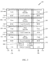
- the global controller 142 includes a read timer 302 in addition to the write timer 152 of the first embodiment.
- the read timer 302 allows the memory 100 to determine independently when read and write operations complete and thus to take appropriate actions based on the actual termination times. For example, if it is determined using the read timer 302 that a read operation has terminated, it may be possible to begin appropriate precharging of a read bit line without waiting for the writing operation to complete.
- the memory 100 thus provides the benefit of allowing simultaneous read and write operations to different memory banks of a multi-bank memory which is formed of single-port memory elements. This provides many of the benefits of dual- or multi-port memory and allows for simultaneous read and write operations as long as simultaneous operations on the same memory bank are prevented.
- Memories according to disclosed embodiments may be formed or integrated into one or more semiconductor dies and/or into various devices, including, without limitation, a set top box, a music player, a video player, an entertainment unit, a navigation device, a communications device, a personal digital assistant (PDA), a fixed location data unit, and a computer.
- a set top box a music player, a video player, an entertainment unit, a navigation device, a communications device, a personal digital assistant (PDA), a fixed location data unit, and a computer.
- PDA personal digital assistant
- a method includes a block 400 of providing a multi-bank memory having at least first and second memory banks, a block 402 of providing at least first and second local controllers adapted to control read and write operations on the at least first and second memory banks, a block 404 of providing a global controller in communication with the at least first and second local controllers, a block 406 of providing the global controller with a first instruction comprising a first memory address and a first operation to be performed at the first memory address, a block 408 of providing the global controller with a second instruction comprising a second memory address and a second operation to be performed at the second memory address, and a block 410 of the global controller instructing the first local controller to perform the first operation at the first memory address and instructing the second local controller to perform the second operation at the second memory address.
- FIG. 5 Another method according to an additional embodiment is illustrated in Figure 5 and includes a block 500 of providing a multi-bank memory having at least first and second memory banks, each of the first and second memory banks comprising a plurality of single-port memory elements, a block 502 of providing first and second local controllers for controlling read and write operations to the at least first and second memory banks, a block 504 of providing a global controller for sending read and write instructions to the first and second local controllers, and a block 506 of sending a read instruction to the first local controller and sending a write instruction to the second local controller at the same time.
- a software module may reside in RAM memory, flash memory, ROM memory, EPROM memory, EEPROM memory, registers, hard disk, a removable disk, a CD-ROM, or any other form of storage medium known in the art.
- An exemplary storage medium is coupled to the processor such that the processor can read information from, and write information to, the storage medium. In the alternative, the storage medium may be integral to the processor.
Landscapes
- Engineering & Computer Science (AREA)
- Theoretical Computer Science (AREA)
- Physics & Mathematics (AREA)
- General Engineering & Computer Science (AREA)
- General Physics & Mathematics (AREA)
- Static Random-Access Memory (AREA)
- Read Only Memory (AREA)
- Dram (AREA)
- Data Exchanges In Wide-Area Networks (AREA)
- Memory System (AREA)
- Techniques For Improving Reliability Of Storages (AREA)
Applications Claiming Priority (3)
| Application Number | Priority Date | Filing Date | Title |
|---|---|---|---|
| US13/297,771 US8699277B2 (en) | 2011-11-16 | 2011-11-16 | Memory configured to provide simultaneous read/write access to multiple banks |
| EP12808934.9A EP2780813B1 (en) | 2011-11-16 | 2012-11-16 | Memory configured to provide simultaneous read/write access to multiple banks |
| PCT/US2012/065658 WO2013075013A1 (en) | 2011-11-16 | 2012-11-16 | Memory configured to provide simultaneous read/write access to multiple banks |
Related Parent Applications (1)
| Application Number | Title | Priority Date | Filing Date |
|---|---|---|---|
| EP12808934.9A Division EP2780813B1 (en) | 2011-11-16 | 2012-11-16 | Memory configured to provide simultaneous read/write access to multiple banks |
Publications (2)
| Publication Number | Publication Date |
|---|---|
| EP3082048A1 EP3082048A1 (en) | 2016-10-19 |
| EP3082048B1 true EP3082048B1 (en) | 2018-10-03 |
Family
ID=47470109
Family Applications (2)
| Application Number | Title | Priority Date | Filing Date |
|---|---|---|---|
| EP16160755.1A Active EP3082048B1 (en) | 2011-11-16 | 2012-11-16 | Memory configured to provide simultaneous read/write access to multiple banks |
| EP12808934.9A Active EP2780813B1 (en) | 2011-11-16 | 2012-11-16 | Memory configured to provide simultaneous read/write access to multiple banks |
Family Applications After (1)
| Application Number | Title | Priority Date | Filing Date |
|---|---|---|---|
| EP12808934.9A Active EP2780813B1 (en) | 2011-11-16 | 2012-11-16 | Memory configured to provide simultaneous read/write access to multiple banks |
Country Status (10)
| Country | Link |
|---|---|
| US (1) | US8699277B2 (https=) |
| EP (2) | EP3082048B1 (https=) |
| JP (1) | JP5852259B2 (https=) |
| KR (1) | KR101669945B1 (https=) |
| CN (1) | CN104081372B (https=) |
| BR (1) | BR112014011806B1 (https=) |
| ES (2) | ES2700854T3 (https=) |
| HU (1) | HUE028961T2 (https=) |
| IN (1) | IN2014CN03730A (https=) |
| WO (1) | WO2013075013A1 (https=) |
Families Citing this family (8)
| Publication number | Priority date | Publication date | Assignee | Title |
|---|---|---|---|---|
| WO2013014841A1 (ja) * | 2011-07-22 | 2013-01-31 | パナソニック株式会社 | データ処理装置およびデータ処理方法 |
| US10719237B2 (en) | 2016-01-11 | 2020-07-21 | Micron Technology, Inc. | Apparatuses and methods for concurrently accessing multiple partitions of a non-volatile memory |
| US10140044B2 (en) * | 2016-03-31 | 2018-11-27 | Qualcomm Incorporated | Efficient memory bank design |
| US11294594B2 (en) * | 2017-08-07 | 2022-04-05 | Kioxia Corporation | SSD architecture supporting low latency operation |
| US11113006B2 (en) | 2019-05-06 | 2021-09-07 | Micron Technology, Inc. | Dynamic data placement for collision avoidance among concurrent write streams |
| US11113198B2 (en) | 2019-05-06 | 2021-09-07 | Micron Technology, Inc. | Timed data transfer between a host system and a memory sub-system |
| US11776591B2 (en) * | 2019-09-26 | 2023-10-03 | Arm Limited | Concurrent access techniques utilizing wordlines with the same row address in single port memory |
| US11386937B2 (en) | 2019-10-12 | 2022-07-12 | Arm Limited | System device and method for providing single port memory access in bitcell array by tracking dummy wordline |
Family Cites Families (22)
| Publication number | Priority date | Publication date | Assignee | Title |
|---|---|---|---|---|
| KR0145224B1 (ko) | 1995-05-27 | 1998-08-17 | 김광호 | 불휘발성 반도체 메모리의 분리된 기입 및 독출 경로를 가지는 워드라인 구동회로 |
| US5996051A (en) | 1997-04-14 | 1999-11-30 | Advanced Micro Devices, Inc. | Communication system which in a first mode supports concurrent memory acceses of a partitioned memory array and in a second mode supports non-concurrent memory accesses to the entire memory array |
| US6009501A (en) * | 1997-06-18 | 1999-12-28 | Micron Technology, Inc. | Method and apparatus for local control signal generation in a memory device |
| CA2239426A1 (en) | 1998-06-03 | 1999-12-03 | Newbridge Networks Corporation | Shared memory system |
| JP2000276400A (ja) * | 1999-03-25 | 2000-10-06 | Univ Hiroshima | アドレス及びデータ転送回路 |
| US6412030B1 (en) | 1999-04-16 | 2002-06-25 | Koninklijke Philips Electronics N.V. | System and method to optimize read performance while accepting write data in a PCI bus architecture |
| CN1282925A (zh) * | 1999-07-12 | 2001-02-07 | 松下电器产业株式会社 | 数据处理装置 |
| US6377492B1 (en) | 2001-03-19 | 2002-04-23 | Etron Technologies, Inc. | Memory architecture for read and write at the same time using a conventional cell |
| US7738496B1 (en) | 2002-12-31 | 2010-06-15 | Cypress Semiconductor Corporation | Device that provides the functionality of dual-ported memory using single-ported memory for multiple clock domains |
| JP4413524B2 (ja) * | 2003-05-01 | 2010-02-10 | 株式会社東芝 | マルチポートメモリ |
| JP2005242929A (ja) * | 2004-02-27 | 2005-09-08 | Fujitsu Ltd | 共有メモリのアクセス方法及びデータ処理装置 |
| US20070028027A1 (en) | 2005-07-26 | 2007-02-01 | Micron Technology, Inc. | Memory device and method having separate write data and read data buses |
| US7533222B2 (en) | 2006-06-29 | 2009-05-12 | Mosys, Inc. | Dual-port SRAM memory using single-port memory cell |
| JP4205743B2 (ja) * | 2006-08-22 | 2009-01-07 | エルピーダメモリ株式会社 | 半導体記憶装置及び半導体装置 |
| US7523228B2 (en) * | 2006-09-18 | 2009-04-21 | International Business Machines Corporation | Method for performing a direct memory access block move in a direct memory access device |
| US7551512B2 (en) | 2007-07-30 | 2009-06-23 | Agere Systems Inc. | Dual-port memory |
| US7739433B2 (en) | 2008-03-05 | 2010-06-15 | Microchip Technology Incorporated | Sharing bandwidth of a single port SRAM between at least one DMA peripheral and a CPU operating with a quadrature clock |
| US7760562B2 (en) | 2008-03-13 | 2010-07-20 | Qualcomm Incorporated | Address multiplexing in pseudo-dual port memory |
| US8140739B2 (en) * | 2008-08-08 | 2012-03-20 | Imation Corp. | Flash memory based storage devices utilizing magnetoresistive random access memory (MRAM) to store files having logical block addresses stored in a write frequency file buffer table |
| US8164974B2 (en) * | 2009-02-24 | 2012-04-24 | Taiwan Semiconductor Manufacturing Company, Ltd. | Memory circuits, systems, and method of interleaving accesses thereof |
| US8331123B2 (en) * | 2009-09-21 | 2012-12-11 | Ocz Technology Group, Inc. | High performance solid-state drives and methods therefor |
| US8375173B2 (en) * | 2009-10-09 | 2013-02-12 | Qualcomm Incorporated | Accessing a multi-channel memory system having non-uniform page sizes |
-
2011
- 2011-11-16 US US13/297,771 patent/US8699277B2/en active Active
-
2012
- 2012-11-16 ES ES16160755T patent/ES2700854T3/es active Active
- 2012-11-16 BR BR112014011806-0A patent/BR112014011806B1/pt active IP Right Grant
- 2012-11-16 CN CN201280066367.2A patent/CN104081372B/zh active Active
- 2012-11-16 EP EP16160755.1A patent/EP3082048B1/en active Active
- 2012-11-16 HU HUE12808934A patent/HUE028961T2/en unknown
- 2012-11-16 EP EP12808934.9A patent/EP2780813B1/en active Active
- 2012-11-16 IN IN3730CHN2014 patent/IN2014CN03730A/en unknown
- 2012-11-16 WO PCT/US2012/065658 patent/WO2013075013A1/en not_active Ceased
- 2012-11-16 KR KR1020147016345A patent/KR101669945B1/ko active Active
- 2012-11-16 JP JP2014542515A patent/JP5852259B2/ja active Active
- 2012-11-16 ES ES12808934.9T patent/ES2575095T3/es active Active
Non-Patent Citations (1)
| Title |
|---|
| None * |
Also Published As
| Publication number | Publication date |
|---|---|
| EP3082048A1 (en) | 2016-10-19 |
| US8699277B2 (en) | 2014-04-15 |
| EP2780813B1 (en) | 2016-04-06 |
| ES2700854T3 (es) | 2019-02-19 |
| BR112014011806B1 (pt) | 2021-01-26 |
| CN104081372A (zh) | 2014-10-01 |
| US20130121086A1 (en) | 2013-05-16 |
| JP2014533861A (ja) | 2014-12-15 |
| EP2780813A1 (en) | 2014-09-24 |
| HUE028961T2 (en) | 2017-02-28 |
| KR101669945B1 (ko) | 2016-10-27 |
| IN2014CN03730A (https=) | 2015-07-03 |
| CN104081372B (zh) | 2017-06-13 |
| WO2013075013A1 (en) | 2013-05-23 |
| JP5852259B2 (ja) | 2016-02-03 |
| BR112014011806A2 (pt) | 2017-05-16 |
| KR20140098792A (ko) | 2014-08-08 |
| ES2575095T3 (es) | 2016-06-24 |
Similar Documents
| Publication | Publication Date | Title |
|---|---|---|
| EP3082048B1 (en) | Memory configured to provide simultaneous read/write access to multiple banks | |
| EP2467852B1 (en) | Atomic memory device | |
| US9158683B2 (en) | Multiport memory emulation using single-port memory devices | |
| US7349285B2 (en) | Dual port memory unit using a single port memory core | |
| US20140195764A1 (en) | Memory device having an adaptable number of open rows | |
| KR20070080844A (ko) | 비휘발성 메모리 제어기 및 휘발성 메모리에 액세스하는방법 및 시스템, 비휘발성 메모리 제어기 및 휘발성 메모리 | |
| KR20070059462A (ko) | 메모리 시스템 및 그것의 부팅 방법 | |
| EP4323877B1 (en) | Adaptive memory access management | |
| CN1988034B (zh) | 具有在端口间的数据发送模式的多径访问半导体存储器件 | |
| US9208856B2 (en) | Multiport memory with matching address control | |
| US6360307B1 (en) | Circuit architecture and method of writing data to a memory | |
| US11003396B2 (en) | Dual speed memory | |
| KR101110550B1 (ko) | 프로세서 장치, 멀티 프로세서 시스템 및 멀티 프로세서 시스템의 공유메모리 접근 방법 | |
| JP4783501B2 (ja) | 半導体記憶装置 | |
| US20170075571A1 (en) | Memory device and control method thereof | |
| US8848480B1 (en) | Synchronous multiple port memory with asynchronous ports | |
| US20200097208A1 (en) | Direct data transfer in memory and between devices of a memory module | |
| US8971145B2 (en) | Synchronous multiple port memory with asynchronous ports | |
| KR100886179B1 (ko) | 듀얼 포트 메모리로의 액세스 권한 획득 처리 방법 및 이를위한 장치 | |
| US8074096B2 (en) | Semiconductor integrated circuit, memory system, memory controller and memory control method | |
| KR100827720B1 (ko) | 접근 제어 장치를 가지는 듀얼 포트 메모리, 듀얼 포트메모리를 가지는 메모리 시스템 및 듀얼 포트 메모리의접근 제어 방법 | |
| KR100813133B1 (ko) | 듀얼 포트 메모리 장치, 이를 가지는 메모리 시스템 및듀얼 포트 메모리 장치의 공유 메모리 영역의 적응적사용방법 | |
| KR20100011012A (ko) | 듀얼 포트 메모리 및 듀얼 포트 메모리의 공유 뱅크 접근제어방법 | |
| KR20080046067A (ko) | 메모리 시스템 및 듀얼 포트 메모리의 접근 제어 방법 | |
| JP2000207273A (ja) | メモリ制御方式 |
Legal Events
| Date | Code | Title | Description |
|---|---|---|---|
| PUAI | Public reference made under article 153(3) epc to a published international application that has entered the european phase |
Free format text: ORIGINAL CODE: 0009012 |
|
| 17P | Request for examination filed |
Effective date: 20160316 |
|
| AC | Divisional application: reference to earlier application |
Ref document number: 2780813 Country of ref document: EP Kind code of ref document: P |
|
| AK | Designated contracting states |
Kind code of ref document: A1 Designated state(s): AL AT BE BG CH CY CZ DE DK EE ES FI FR GB GR HR HU IE IS IT LI LT LU LV MC MK MT NL NO PL PT RO RS SE SI SK SM TR |
|
| 17Q | First examination report despatched |
Effective date: 20170906 |
|
| GRAP | Despatch of communication of intention to grant a patent |
Free format text: ORIGINAL CODE: EPIDOSNIGR1 |
|
| INTG | Intention to grant announced |
Effective date: 20180503 |
|
| GRAS | Grant fee paid |
Free format text: ORIGINAL CODE: EPIDOSNIGR3 |
|
| GRAA | (expected) grant |
Free format text: ORIGINAL CODE: 0009210 |
|
| AC | Divisional application: reference to earlier application |
Ref document number: 2780813 Country of ref document: EP Kind code of ref document: P |
|
| AK | Designated contracting states |
Kind code of ref document: B1 Designated state(s): AL AT BE BG CH CY CZ DE DK EE ES FI FR GB GR HR HU IE IS IT LI LT LU LV MC MK MT NL NO PL PT RO RS SE SI SK SM TR |
|
| REG | Reference to a national code |
Ref country code: GB Ref legal event code: FG4D |
|
| REG | Reference to a national code |
Ref country code: FR Ref legal event code: PLFP Year of fee payment: 7 |
|
| REG | Reference to a national code |
Ref country code: CH Ref legal event code: EP Ref country code: AT Ref legal event code: REF Ref document number: 1049361 Country of ref document: AT Kind code of ref document: T Effective date: 20181015 |
|
| REG | Reference to a national code |
Ref country code: DE Ref legal event code: R096 Ref document number: 602012051920 Country of ref document: DE Ref country code: IE Ref legal event code: FG4D |
|
| REG | Reference to a national code |
Ref country code: NL Ref legal event code: FP |
|
| REG | Reference to a national code |
Ref country code: ES Ref legal event code: FG2A Ref document number: 2700854 Country of ref document: ES Kind code of ref document: T3 Effective date: 20190219 |
|
| REG | Reference to a national code |
Ref country code: LT Ref legal event code: MG4D |
|
| REG | Reference to a national code |
Ref country code: AT Ref legal event code: MK05 Ref document number: 1049361 Country of ref document: AT Kind code of ref document: T Effective date: 20181003 |
|
| PG25 | Lapsed in a contracting state [announced via postgrant information from national office to epo] |
Ref country code: LV Free format text: LAPSE BECAUSE OF FAILURE TO SUBMIT A TRANSLATION OF THE DESCRIPTION OR TO PAY THE FEE WITHIN THE PRESCRIBED TIME-LIMIT Effective date: 20181003 Ref country code: PL Free format text: LAPSE BECAUSE OF FAILURE TO SUBMIT A TRANSLATION OF THE DESCRIPTION OR TO PAY THE FEE WITHIN THE PRESCRIBED TIME-LIMIT Effective date: 20181003 Ref country code: HR Free format text: LAPSE BECAUSE OF FAILURE TO SUBMIT A TRANSLATION OF THE DESCRIPTION OR TO PAY THE FEE WITHIN THE PRESCRIBED TIME-LIMIT Effective date: 20181003 Ref country code: IS Free format text: LAPSE BECAUSE OF FAILURE TO SUBMIT A TRANSLATION OF THE DESCRIPTION OR TO PAY THE FEE WITHIN THE PRESCRIBED TIME-LIMIT Effective date: 20190203 Ref country code: BG Free format text: LAPSE BECAUSE OF FAILURE TO SUBMIT A TRANSLATION OF THE DESCRIPTION OR TO PAY THE FEE WITHIN THE PRESCRIBED TIME-LIMIT Effective date: 20190103 Ref country code: NO Free format text: LAPSE BECAUSE OF FAILURE TO SUBMIT A TRANSLATION OF THE DESCRIPTION OR TO PAY THE FEE WITHIN THE PRESCRIBED TIME-LIMIT Effective date: 20190103 Ref country code: LT Free format text: LAPSE BECAUSE OF FAILURE TO SUBMIT A TRANSLATION OF THE DESCRIPTION OR TO PAY THE FEE WITHIN THE PRESCRIBED TIME-LIMIT Effective date: 20181003 Ref country code: AT Free format text: LAPSE BECAUSE OF FAILURE TO SUBMIT A TRANSLATION OF THE DESCRIPTION OR TO PAY THE FEE WITHIN THE PRESCRIBED TIME-LIMIT Effective date: 20181003 Ref country code: CZ Free format text: LAPSE BECAUSE OF FAILURE TO SUBMIT A TRANSLATION OF THE DESCRIPTION OR TO PAY THE FEE WITHIN THE PRESCRIBED TIME-LIMIT Effective date: 20181003 |
|
| PG25 | Lapsed in a contracting state [announced via postgrant information from national office to epo] |
Ref country code: SE Free format text: LAPSE BECAUSE OF FAILURE TO SUBMIT A TRANSLATION OF THE DESCRIPTION OR TO PAY THE FEE WITHIN THE PRESCRIBED TIME-LIMIT Effective date: 20181003 Ref country code: RS Free format text: LAPSE BECAUSE OF FAILURE TO SUBMIT A TRANSLATION OF THE DESCRIPTION OR TO PAY THE FEE WITHIN THE PRESCRIBED TIME-LIMIT Effective date: 20181003 Ref country code: PT Free format text: LAPSE BECAUSE OF FAILURE TO SUBMIT A TRANSLATION OF THE DESCRIPTION OR TO PAY THE FEE WITHIN THE PRESCRIBED TIME-LIMIT Effective date: 20190203 Ref country code: GR Free format text: LAPSE BECAUSE OF FAILURE TO SUBMIT A TRANSLATION OF THE DESCRIPTION OR TO PAY THE FEE WITHIN THE PRESCRIBED TIME-LIMIT Effective date: 20190104 Ref country code: AL Free format text: LAPSE BECAUSE OF FAILURE TO SUBMIT A TRANSLATION OF THE DESCRIPTION OR TO PAY THE FEE WITHIN THE PRESCRIBED TIME-LIMIT Effective date: 20181003 |
|
| REG | Reference to a national code |
Ref country code: CH Ref legal event code: PL |
|
| REG | Reference to a national code |
Ref country code: DE Ref legal event code: R097 Ref document number: 602012051920 Country of ref document: DE |
|
| PG25 | Lapsed in a contracting state [announced via postgrant information from national office to epo] |
Ref country code: DK Free format text: LAPSE BECAUSE OF FAILURE TO SUBMIT A TRANSLATION OF THE DESCRIPTION OR TO PAY THE FEE WITHIN THE PRESCRIBED TIME-LIMIT Effective date: 20181003 Ref country code: LU Free format text: LAPSE BECAUSE OF NON-PAYMENT OF DUE FEES Effective date: 20181116 |
|
| PLBE | No opposition filed within time limit |
Free format text: ORIGINAL CODE: 0009261 |
|
| STAA | Information on the status of an ep patent application or granted ep patent |
Free format text: STATUS: NO OPPOSITION FILED WITHIN TIME LIMIT |
|
| REG | Reference to a national code |
Ref country code: BE Ref legal event code: MM Effective date: 20181130 |
|
| REG | Reference to a national code |
Ref country code: IE Ref legal event code: MM4A |
|
| PG25 | Lapsed in a contracting state [announced via postgrant information from national office to epo] |
Ref country code: SK Free format text: LAPSE BECAUSE OF FAILURE TO SUBMIT A TRANSLATION OF THE DESCRIPTION OR TO PAY THE FEE WITHIN THE PRESCRIBED TIME-LIMIT Effective date: 20181003 Ref country code: RO Free format text: LAPSE BECAUSE OF FAILURE TO SUBMIT A TRANSLATION OF THE DESCRIPTION OR TO PAY THE FEE WITHIN THE PRESCRIBED TIME-LIMIT Effective date: 20181003 Ref country code: MC Free format text: LAPSE BECAUSE OF FAILURE TO SUBMIT A TRANSLATION OF THE DESCRIPTION OR TO PAY THE FEE WITHIN THE PRESCRIBED TIME-LIMIT Effective date: 20181003 Ref country code: EE Free format text: LAPSE BECAUSE OF FAILURE TO SUBMIT A TRANSLATION OF THE DESCRIPTION OR TO PAY THE FEE WITHIN THE PRESCRIBED TIME-LIMIT Effective date: 20181003 Ref country code: CH Free format text: LAPSE BECAUSE OF NON-PAYMENT OF DUE FEES Effective date: 20181130 Ref country code: SM Free format text: LAPSE BECAUSE OF FAILURE TO SUBMIT A TRANSLATION OF THE DESCRIPTION OR TO PAY THE FEE WITHIN THE PRESCRIBED TIME-LIMIT Effective date: 20181003 Ref country code: LI Free format text: LAPSE BECAUSE OF NON-PAYMENT OF DUE FEES Effective date: 20181130 |
|
| 26N | No opposition filed |
Effective date: 20190704 |
|
| PG25 | Lapsed in a contracting state [announced via postgrant information from national office to epo] |
Ref country code: IE Free format text: LAPSE BECAUSE OF NON-PAYMENT OF DUE FEES Effective date: 20181116 Ref country code: SI Free format text: LAPSE BECAUSE OF FAILURE TO SUBMIT A TRANSLATION OF THE DESCRIPTION OR TO PAY THE FEE WITHIN THE PRESCRIBED TIME-LIMIT Effective date: 20181003 |
|
| PG25 | Lapsed in a contracting state [announced via postgrant information from national office to epo] |
Ref country code: BE Free format text: LAPSE BECAUSE OF NON-PAYMENT OF DUE FEES Effective date: 20181130 |
|
| PG25 | Lapsed in a contracting state [announced via postgrant information from national office to epo] |
Ref country code: MT Free format text: LAPSE BECAUSE OF NON-PAYMENT OF DUE FEES Effective date: 20181116 |
|
| PG25 | Lapsed in a contracting state [announced via postgrant information from national office to epo] |
Ref country code: TR Free format text: LAPSE BECAUSE OF FAILURE TO SUBMIT A TRANSLATION OF THE DESCRIPTION OR TO PAY THE FEE WITHIN THE PRESCRIBED TIME-LIMIT Effective date: 20181003 |
|
| PG25 | Lapsed in a contracting state [announced via postgrant information from national office to epo] |
Ref country code: MK Free format text: LAPSE BECAUSE OF NON-PAYMENT OF DUE FEES Effective date: 20181003 Ref country code: CY Free format text: LAPSE BECAUSE OF FAILURE TO SUBMIT A TRANSLATION OF THE DESCRIPTION OR TO PAY THE FEE WITHIN THE PRESCRIBED TIME-LIMIT Effective date: 20181003 |
|
| PGFP | Annual fee paid to national office [announced via postgrant information from national office to epo] |
Ref country code: NL Payment date: 20251015 Year of fee payment: 14 |
|
| PGFP | Annual fee paid to national office [announced via postgrant information from national office to epo] |
Ref country code: HU Payment date: 20251106 Year of fee payment: 14 |
|
| PGFP | Annual fee paid to national office [announced via postgrant information from national office to epo] |
Ref country code: DE Payment date: 20251013 Year of fee payment: 14 |
|
| PGFP | Annual fee paid to national office [announced via postgrant information from national office to epo] |
Ref country code: GB Payment date: 20251009 Year of fee payment: 14 |
|
| PGFP | Annual fee paid to national office [announced via postgrant information from national office to epo] |
Ref country code: IT Payment date: 20251117 Year of fee payment: 14 Ref country code: FI Payment date: 20251029 Year of fee payment: 14 |
|
| PGFP | Annual fee paid to national office [announced via postgrant information from national office to epo] |
Ref country code: FR Payment date: 20251013 Year of fee payment: 14 |
|
| PGFP | Annual fee paid to national office [announced via postgrant information from national office to epo] |
Ref country code: ES Payment date: 20251209 Year of fee payment: 14 |