EP3067722B1 - Polarisator und anzeigevorrichtung damit - Google Patents
Polarisator und anzeigevorrichtung damit Download PDFInfo
- Publication number
- EP3067722B1 EP3067722B1 EP16158811.6A EP16158811A EP3067722B1 EP 3067722 B1 EP3067722 B1 EP 3067722B1 EP 16158811 A EP16158811 A EP 16158811A EP 3067722 B1 EP3067722 B1 EP 3067722B1
- Authority
- EP
- European Patent Office
- Prior art keywords
- polarizer
- layer
- wave plate
- refractive index
- electrode
- Prior art date
- Legal status (The legal status is an assumption and is not a legal conclusion. Google has not performed a legal analysis and makes no representation as to the accuracy of the status listed.)
- Active
Links
Images



Classifications
-
- G—PHYSICS
- G02—OPTICS
- G02B—OPTICAL ELEMENTS, SYSTEMS OR APPARATUS
- G02B5/00—Optical elements other than lenses
- G02B5/30—Polarising elements
- G02B5/3083—Birefringent or phase retarding elements
-
- G—PHYSICS
- G02—OPTICS
- G02B—OPTICAL ELEMENTS, SYSTEMS OR APPARATUS
- G02B27/00—Optical systems or apparatus not provided for by any of the groups G02B1/00 - G02B26/00, G02B30/00
- G02B27/28—Optical systems or apparatus not provided for by any of the groups G02B1/00 - G02B26/00, G02B30/00 for polarising
- G02B27/286—Optical systems or apparatus not provided for by any of the groups G02B1/00 - G02B26/00, G02B30/00 for polarising for controlling or changing the state of polarisation, e.g. transforming one polarisation state into another
-
- G—PHYSICS
- G02—OPTICS
- G02B—OPTICAL ELEMENTS, SYSTEMS OR APPARATUS
- G02B5/00—Optical elements other than lenses
- G02B5/30—Polarising elements
- G02B5/3016—Polarising elements involving passive liquid crystal elements
-
- G—PHYSICS
- G02—OPTICS
- G02B—OPTICAL ELEMENTS, SYSTEMS OR APPARATUS
- G02B5/00—Optical elements other than lenses
- G02B5/30—Polarising elements
- G02B5/3025—Polarisers, i.e. arrangements capable of producing a definite output polarisation state from an unpolarised input state
-
- G—PHYSICS
- G02—OPTICS
- G02F—OPTICAL DEVICES OR ARRANGEMENTS FOR THE CONTROL OF LIGHT BY MODIFICATION OF THE OPTICAL PROPERTIES OF THE MEDIA OF THE ELEMENTS INVOLVED THEREIN; NON-LINEAR OPTICS; FREQUENCY-CHANGING OF LIGHT; OPTICAL LOGIC ELEMENTS; OPTICAL ANALOGUE/DIGITAL CONVERTERS
- G02F1/00—Devices or arrangements for the control of the intensity, colour, phase, polarisation or direction of light arriving from an independent light source, e.g. switching, gating or modulating; Non-linear optics
- G02F1/01—Devices or arrangements for the control of the intensity, colour, phase, polarisation or direction of light arriving from an independent light source, e.g. switching, gating or modulating; Non-linear optics for the control of the intensity, phase, polarisation or colour
- G02F1/13—Devices or arrangements for the control of the intensity, colour, phase, polarisation or direction of light arriving from an independent light source, e.g. switching, gating or modulating; Non-linear optics for the control of the intensity, phase, polarisation or colour based on liquid crystals, e.g. single liquid crystal display cells
- G02F1/133—Constructional arrangements; Operation of liquid crystal cells; Circuit arrangements
- G02F1/1333—Constructional arrangements; Manufacturing methods
- G02F1/1335—Structural association of cells with optical devices, e.g. polarisers or reflectors
- G02F1/133528—Polarisers
-
- G—PHYSICS
- G02—OPTICS
- G02F—OPTICAL DEVICES OR ARRANGEMENTS FOR THE CONTROL OF LIGHT BY MODIFICATION OF THE OPTICAL PROPERTIES OF THE MEDIA OF THE ELEMENTS INVOLVED THEREIN; NON-LINEAR OPTICS; FREQUENCY-CHANGING OF LIGHT; OPTICAL LOGIC ELEMENTS; OPTICAL ANALOGUE/DIGITAL CONVERTERS
- G02F1/00—Devices or arrangements for the control of the intensity, colour, phase, polarisation or direction of light arriving from an independent light source, e.g. switching, gating or modulating; Non-linear optics
- G02F1/01—Devices or arrangements for the control of the intensity, colour, phase, polarisation or direction of light arriving from an independent light source, e.g. switching, gating or modulating; Non-linear optics for the control of the intensity, phase, polarisation or colour
- G02F1/13—Devices or arrangements for the control of the intensity, colour, phase, polarisation or direction of light arriving from an independent light source, e.g. switching, gating or modulating; Non-linear optics for the control of the intensity, phase, polarisation or colour based on liquid crystals, e.g. single liquid crystal display cells
- G02F1/133—Constructional arrangements; Operation of liquid crystal cells; Circuit arrangements
- G02F1/1333—Constructional arrangements; Manufacturing methods
- G02F1/1335—Structural association of cells with optical devices, e.g. polarisers or reflectors
- G02F1/13363—Birefringent elements, e.g. for optical compensation
- G02F1/133634—Birefringent elements, e.g. for optical compensation the refractive index Nz perpendicular to the element surface being different from in-plane refractive indices Nx and Ny, e.g. biaxial or with normal optical axis
-
- H—ELECTRICITY
- H10—SEMICONDUCTOR DEVICES; ELECTRIC SOLID-STATE DEVICES NOT OTHERWISE PROVIDED FOR
- H10K—ORGANIC ELECTRIC SOLID-STATE DEVICES
- H10K50/00—Organic light-emitting devices
- H10K50/80—Constructional details
- H10K50/84—Passivation; Containers; Encapsulations
-
- H—ELECTRICITY
- H10—SEMICONDUCTOR DEVICES; ELECTRIC SOLID-STATE DEVICES NOT OTHERWISE PROVIDED FOR
- H10K—ORGANIC ELECTRIC SOLID-STATE DEVICES
- H10K50/00—Organic light-emitting devices
- H10K50/80—Constructional details
- H10K50/85—Arrangements for extracting light from the devices
- H10K50/858—Arrangements for extracting light from the devices comprising refractive means, e.g. lenses
-
- H—ELECTRICITY
- H10—SEMICONDUCTOR DEVICES; ELECTRIC SOLID-STATE DEVICES NOT OTHERWISE PROVIDED FOR
- H10K—ORGANIC ELECTRIC SOLID-STATE DEVICES
- H10K50/00—Organic light-emitting devices
- H10K50/80—Constructional details
- H10K50/86—Arrangements for improving contrast, e.g. preventing reflection of ambient light
-
- H—ELECTRICITY
- H10—SEMICONDUCTOR DEVICES; ELECTRIC SOLID-STATE DEVICES NOT OTHERWISE PROVIDED FOR
- H10K—ORGANIC ELECTRIC SOLID-STATE DEVICES
- H10K59/00—Integrated devices, or assemblies of multiple devices, comprising at least one organic light-emitting element covered by group H10K50/00
- H10K59/80—Constructional details
- H10K59/875—Arrangements for extracting light from the devices
- H10K59/879—Arrangements for extracting light from the devices comprising refractive means, e.g. lenses
-
- H—ELECTRICITY
- H10—SEMICONDUCTOR DEVICES; ELECTRIC SOLID-STATE DEVICES NOT OTHERWISE PROVIDED FOR
- H10K—ORGANIC ELECTRIC SOLID-STATE DEVICES
- H10K59/00—Integrated devices, or assemblies of multiple devices, comprising at least one organic light-emitting element covered by group H10K50/00
- H10K59/80—Constructional details
- H10K59/8791—Arrangements for improving contrast, e.g. preventing reflection of ambient light
-
- H—ELECTRICITY
- H10—SEMICONDUCTOR DEVICES; ELECTRIC SOLID-STATE DEVICES NOT OTHERWISE PROVIDED FOR
- H10K—ORGANIC ELECTRIC SOLID-STATE DEVICES
- H10K85/00—Organic materials used in the body or electrodes of devices covered by this subclass
- H10K85/10—Organic polymers or oligomers
- H10K85/141—Organic polymers or oligomers comprising aliphatic or olefinic chains, e.g. poly N-vinylcarbazol, PVC or PTFE
-
- H—ELECTRICITY
- H10—SEMICONDUCTOR DEVICES; ELECTRIC SOLID-STATE DEVICES NOT OTHERWISE PROVIDED FOR
- H10K—ORGANIC ELECTRIC SOLID-STATE DEVICES
- H10K85/00—Organic materials used in the body or electrodes of devices covered by this subclass
- H10K85/731—Liquid crystalline materials
-
- G—PHYSICS
- G02—OPTICS
- G02F—OPTICAL DEVICES OR ARRANGEMENTS FOR THE CONTROL OF LIGHT BY MODIFICATION OF THE OPTICAL PROPERTIES OF THE MEDIA OF THE ELEMENTS INVOLVED THEREIN; NON-LINEAR OPTICS; FREQUENCY-CHANGING OF LIGHT; OPTICAL LOGIC ELEMENTS; OPTICAL ANALOGUE/DIGITAL CONVERTERS
- G02F1/00—Devices or arrangements for the control of the intensity, colour, phase, polarisation or direction of light arriving from an independent light source, e.g. switching, gating or modulating; Non-linear optics
- G02F1/01—Devices or arrangements for the control of the intensity, colour, phase, polarisation or direction of light arriving from an independent light source, e.g. switching, gating or modulating; Non-linear optics for the control of the intensity, phase, polarisation or colour
- G02F1/13—Devices or arrangements for the control of the intensity, colour, phase, polarisation or direction of light arriving from an independent light source, e.g. switching, gating or modulating; Non-linear optics for the control of the intensity, phase, polarisation or colour based on liquid crystals, e.g. single liquid crystal display cells
- G02F1/133—Constructional arrangements; Operation of liquid crystal cells; Circuit arrangements
- G02F1/1333—Constructional arrangements; Manufacturing methods
- G02F1/1335—Structural association of cells with optical devices, e.g. polarisers or reflectors
- G02F1/13363—Birefringent elements, e.g. for optical compensation
- G02F1/133638—Waveplates, i.e. plates with a retardation value of lambda/n
-
- H—ELECTRICITY
- H10—SEMICONDUCTOR DEVICES; ELECTRIC SOLID-STATE DEVICES NOT OTHERWISE PROVIDED FOR
- H10K—ORGANIC ELECTRIC SOLID-STATE DEVICES
- H10K2102/00—Constructional details relating to the organic devices covered by this subclass
- H10K2102/301—Details of OLEDs
- H10K2102/302—Details of OLEDs of OLED structures
- H10K2102/3023—Direction of light emission
- H10K2102/3026—Top emission
-
- H—ELECTRICITY
- H10—SEMICONDUCTOR DEVICES; ELECTRIC SOLID-STATE DEVICES NOT OTHERWISE PROVIDED FOR
- H10K—ORGANIC ELECTRIC SOLID-STATE DEVICES
- H10K2102/00—Constructional details relating to the organic devices covered by this subclass
- H10K2102/301—Details of OLEDs
- H10K2102/351—Thickness
-
- H—ELECTRICITY
- H10—SEMICONDUCTOR DEVICES; ELECTRIC SOLID-STATE DEVICES NOT OTHERWISE PROVIDED FOR
- H10K—ORGANIC ELECTRIC SOLID-STATE DEVICES
- H10K50/00—Organic light-emitting devices
- H10K50/80—Constructional details
- H10K50/84—Passivation; Containers; Encapsulations
- H10K50/844—Encapsulations
- H10K50/8445—Encapsulations multilayered coatings having a repetitive structure, e.g. having multiple organic-inorganic bilayers
-
- H—ELECTRICITY
- H10—SEMICONDUCTOR DEVICES; ELECTRIC SOLID-STATE DEVICES NOT OTHERWISE PROVIDED FOR
- H10K—ORGANIC ELECTRIC SOLID-STATE DEVICES
- H10K59/00—Integrated devices, or assemblies of multiple devices, comprising at least one organic light-emitting element covered by group H10K50/00
- H10K59/10—OLED displays
- H10K59/12—Active-matrix OLED [AMOLED] displays
-
- H—ELECTRICITY
- H10—SEMICONDUCTOR DEVICES; ELECTRIC SOLID-STATE DEVICES NOT OTHERWISE PROVIDED FOR
- H10K—ORGANIC ELECTRIC SOLID-STATE DEVICES
- H10K59/00—Integrated devices, or assemblies of multiple devices, comprising at least one organic light-emitting element covered by group H10K50/00
- H10K59/80—Constructional details
- H10K59/87—Passivation; Containers; Encapsulations
- H10K59/873—Encapsulations
- H10K59/8731—Encapsulations multilayered coatings having a repetitive structure, e.g. having multiple organic-inorganic bilayers
Definitions
- OLED displays generate images without the use of a backlight, unlike a liquid crystal display (LCD), and thus, they can have thinner profile and be lightweight. Further, OLED displays have favorable characteristics, such as low power consumption, high luminance, and rapid response rate, and thus, they have drawn attention as a next generation display device.
- OLED displays generally include various types of electrodes and wirings which reflect light from external sources such as ambient light. Due to such reflection, an OLED display has difficulty in representing the deepest black in a relatively bright environment and exhibits a relatively lower contrast ratio.
- a polarizer film is formed over the pixels.
- US 2009/219472 relates to a liquid crystal display device.
- US 2005/127820 relates to a light-emitting device.
- EP 2541638 relates to an organic light-emitting display apparatus.
- US 2008/291389 relates to an elliptically polarizing plate.
- US 2014/168768 relates to a polarizing plate.
- US 2011/001906 relates to a polarizing plate with built-in viewing angle compensation film.
- One inventive aspect relates to a polarizer that can effectively prevent reflection of external light and a display device including the same.
- the refractive index anisotropic layer can have a thickness in a range of about 1 micrometer ( ⁇ m) to about 5 ⁇ m.
- the half-wave plate can include an alignment layer, and the refractive index anisotropic layer can be disposed on the alignment layer.
- the quarter-wave plate can include a cyclic olefin polymer (COP).
- COP cyclic olefin polymer
- the quarter-wave plate can be disposed on the linear polarizer, and the half-wave plate can be disposed on the quarter-wave plate.
- the half-wave plate can be disposed on the linear polarizer, and the quarter-wave plate can be disposed on the half-wave plate.
- the refractive index anisotropic includes a liquid crystal layer.
- the liquid crystal layer includes a discotic compound.
- the discotic compound has a disc surface, and the disc surface has an inclination angle in a range of about 60 degrees to about 90 degrees with respect to a surface of the half-wave plate.
- Nx and Nz can be in a range of about 1.6 to about 1.8.
- Ny can be in a range of about 1.5 to about 1.7.
- a difference between Nx and Ny can be in a range of about 0.05 to about 0.2.
- the refractive index anisotropic layer can have a thickness in a range of about 1 ⁇ m to about 5 ⁇ m.
- the half-wave plate can further include an alignment layer, and the refractive index anisotropic layer is disposed on the alignment layer.
- the quarter-wave plate can include a COP.
- the quarter-wave plate can be disposed on the linear polarizer, and the half-wave plate can be disposed on the quarter-wave plate.
- the half-wave plate can be disposed on the linear polarizer, and the quarter-wave plate can be disposed on the half-wave plate.
- the display panel can include: a first substrate; a first electrode disposed on the first substrate; an organic light emitting layer disposed on the first electrode; and a second electrode disposed on the organic light emitting layer.
- the display device can further include: a second substrate disposed on the second electrode, wherein the polarizer is disposed on the second substrate.
- the display device can further include: a thin film encapsulation layer disposed on the second electrode, wherein the polarizer is disposed on the thin film encapsulation layer.
- the refractive index anisotropic layer comprises a liquid crystal layer.
- the liquid crystal layer comprises a discotic compound.
- the discotic compound has a disc surface, and wherein the disc surface has an inclination angle in the range of about 60 degrees to about 90 degrees with respect to a surface of the half-wave plate.
- each of Nx and Nz is in the range of about 1.6 to about 1.8.
- Ny is in the range of about 1.5 to about 1.7.
- the difference between Nx and Ny is in the range of about 0.05 to about 0.2.
- the refractive index anisotropic layer has a thickness in the range of about 1 micrometer ( ⁇ m) to about 5 ⁇ m.
- the half-wave plate comprises an alignment layer, and wherein the refractive index anisotropic layer is on the alignment layer.
- the quarter-wave plate comprises a cyclic olefin polymer (COP).
- COP cyclic olefin polymer
- the quarter-wave plate is on the linear polarizer, and wherein the half-wave plate is on the quarter-wave plate.
- the half-wave plate is on the linear polarizer, and wherein the quarter-wave plate is on the half-wave plate.
- the refractive index anisotropic layer comprises a liquid crystal layer.
- the liquid crystal layer comprises a discotic compound.
- the discotic compound has a disc surface, and wherein the disc surface has an inclination angle in the range of about 60 degrees to about 90 degrees with respect to a surface of the half-wave plate.
- each of Nx and Nz is in the range of about 1.6 to about 1.8.
- Ny is in the range of about 1.5 to about 1.7.
- the difference between Nx and Ny is in a range of about 0.05 to about 0.2.
- refractive index anisotropic layer has a thickness in the range of about 1 micrometer ( ⁇ m) to about 5 ⁇ m.
- the half-wave plate further comprises an alignment layer, and wherein the refractive index anisotropic layer is on the alignment layer.
- the quarter-wave plate comprises a cyclic olefin polymer (COP).
- the quarter-wave plate is on the linear polarizer, and wherein the half-wave plate is on the quarter-wave plate.
- the half-wave plate is on the linear polarizer, and wherein the quarter-wave plate is on the half-wave plate.
- the display panel comprises: a first substrate; a first electrode on the first substrate; an organic light emitting layer on the first electrode; and a second electrode on the organic light emitting layer.
- the above display device further comprises a second substrate on the second electrode, wherein the polarizer is on the second substrate.
- the above display device further comprises a thin film encapsulation layer on the second electrode, wherein the polarizer is on the thin film encapsulation layer.
- each of the half-wave and quarter-wave plates is thinner than the linear polarizer.
- a display device as set out in claim 11. Preferred features are set out in claim 12.
- the layer or element When a layer or element is referred to as being "on" another layer or element, the layer or element can be directly on the other layer or element, or one or more intervening layers or elements can be interposed therebetween.
- the term “substantially” includes the meanings of completely, almost completely or to any significant degree under some applications and in accordance with those skilled in the art.
- the term “connected” can include an electrical connection.
- FIGS. 1 through 3 a first exemplary embodiment will be described with reference to FIGS. 1 through 3 .
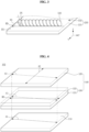
- FIG. 1 is a cross-sectional view illustrating a polarizer 101 according to the first exemplary embodiment.
- FIG. 2 is an exploded perspective view of FIG. 1 .
- the polarizer 101 can include a linear polarizer 110 and a phase retardation layer 140 formed on the linear polarizer 110.
- the polarizer 101 can serve to prevent reflection of external light.
- the linear polarizer 110 can serve to linearly polarize an external light incident on the polarizer 101.
- the linear polarizer 110 can use a film obtained by a dichroic dye being adsorbed onto and aligned in a polyvinyl alcohol (PVA) resin.
- PVA resin can include a homopolymer of vinyl acetate or a copolymer of a monomer different from vinyl acetate.
- the polarizer 110 can be prepared through a scheme including, for example, a process of uniaxially stretching a PVA resin film, a process of dyeing the PVA resin film with a dichroic dye such that the dichroic dye is adsorbed onto the PVA resin film, a process of treating the PVA resin film, onto which the dichroic dye is adsorbed, using a boron aqueous solution, and a washing process.
- a scheme of manufacturing the linear polarizer 110 according to the first exemplary embodiment is not limited thereto.
- the dichroic dye can use, for example, iodine and another dichroic dye used in the pertinent art.
- the linear polarizer 110 can be prepared through a process of dyeing the PVA resin film by immersing the PVA resin film in an aqueous solution containing iodine and potassium iodine.
- Iodine can be arranged in a direction parallel to a direction in which the PVA resin film is stretched.
- a transmission axis A1 of the linear polarizer 110 can be determined based on the arrangement of iodine, and the transmission axis A1 of the linear polarizer 110 can be substantially parallel to the direction of the arrangement of iodine.
- a thickness of the linear polarizer 110 can vary based on a product to which the linear polarizer 110 is to be applied.
- the linear polarizer 110 has a thickness in the range of about 5 micrometers ( ⁇ m) to about 50 ⁇ m.
- the phase retardation layer 140 can be formed on a surface of the linear polarizer 110.
- the phase retardation layer 140 can retard a phase of light.
- the phase retardation layer 140 can convert a linearly polarized light to a circularly polarized light, or can convert a circularly polarized light to a linearly polarized light.
- an external light incident on the polarizer 101 is linearly polarized by the linear polarizer 110, or circularly polarized by the phase retardation layer 140.
- the circularly polarized external light can be reflected within a device to which the polarizer 101 is attached, for example, a display device, to thereby be converted to a reflected light.
- a phase and a polarization axis of the light can vary.
- the reflected light with the varied phase does not pass through the polarizer 101, and thus, reflection of the external light can be prevented by the polarizer 101.
- the phase retardation layer 140 can use a phase difference plate having a film shape. For example, a single layer of the phase difference plate is used, or a plurality of layers of the phase difference plate are stacked to be used.
- the phase retardation layer 140 can include a quarter-wave plate (QWP) 120 and a half-wave plate (HWP) 130.
- QWP quarter-wave plate
- HWP half-wave plate
- the phase retardation layer 140 can include the QWP 120 formed on the linear polarizer 110 and the HWP 130 formed on the QWP 120.
- the first exemplary embodiment is not limited thereto, and the HWP 130 can be formed on the linear polarizer 110 and the QWP 120 can be formed on the HWP 130.
- the QWP 120 can be prepared by stretching a film.
- the QWP 120 is be prepared by stretching a film formed of polycarbonate (PC), polyvinyl alcohol (PVA), polystyrene (PS), poly(methyl methacrylate) (PMMA), polypropylene (PP), polyolefin, polyarylate (PAR), or polyamide (PA).
- the QWP 120 can include a film formed of a cyclic olefin polymer (COP).
- COP cyclic olefin polymer
- the COP film can be prepared using, for example, a norbomene-based COP.
- the COP film can have high light transmittance, high thermal resistance, high strength, low moisture absorption, and high cost-efficiency.
- a phase difference plate formed of such a COP film can represent a relatively stable phase retardation value, irrespective of a wavelength of incident light.
- the QWP 120 can be prepared using a photocurable liquid crystal compound.
- a photocurable liquid crystal compound For example, an alignment layer is formed on a base film, and liquid crystal compounds is arranged on the alignment layer to be patterned thereon, such that the QWP 120 can be prepared.
- the type of the phase difference plate to be prepared that is, whether the quarter-wave plate or the half-wave plate, can be determined.
- the type or the manufacturing scheme of the QWP 120 is not limited to the above description in embodiments of the invention.
- the QWP 120 can have a transmission axis A2.
- the transmission axis A2 of the QWP 120 can be determined by a stretching axis of a film or a direction in which the liquid crystal compounds are aligned.
- the QWP 120 according to the first exemplary embodiment can be prepared by stretching the COP film, and the transmission axis A2 of the QWP 120 can be substantially parallel to a stretching axis of the COP film.
- the QWP 120 according to the first exemplary embodiment can be designed to be optimized for preventing reflection of an external light incident frontwards, that is, an external light vertically incident on a surface of the polarizer 101. Accordingly, in a case of a polarizer using only the QWP 120 as the phase retardation layer 140, reflection of an external light incident on the polarizer at a predetermined incident angle is not effectively prevented by the polarizer. In other words, in the case of using only the QWP 120 as the phase retardation layer 140, a path of an external light can vary based on an incident angle of the external light such that a phase retardation effect can change, and the effect of preventing reflection of the external light can also change based on the incident angle.
- the HWP 130 can be used along with the QWP 120.
- the HWP 130 according to the first exemplary embodiment can have a refractive index anisotropic layer.
- FIG. 3 is a structural view illustrating the HWP 130.
- the HWP 130 of FIG. 3 can include a liquid crystal layer 132 as the refractive index anisotropic layer.
- the HWP 130 can include a support member 131 and the liquid crystal layer 132 formed on the support member 131.
- the liquid crystal layer 132 can have a refractive index anisotropy.
- the support member 131 can serve to support the liquid crystal layer 132.
- the support member 131 can be formed of a transparent plastic film and can include, for example, one or more of the following materials: tri-acetyl cellulose (TAC), polyethylene terephthalate (PET), polyimide (PI), and polycarbonate (PC).
- TAC tri-acetyl cellulose
- PET polyethylene terephthalate
- PI polyimide
- PC polycarbonate
- an alignment layer can be used as the support member 131.
- a description pertaining to the alignment layer will be provided further below.
- the liquid crystal layer 132 includes a discotic compound 133.
- the liquid crystal layer 132 can include a binder compound, and the discotic compounds 133 can be arranged through being dispersed in the binder compound.
- the liquid crystal layer 132 including the discotic compound 133 can also be referred to as a discotic liquid crystal layer.
- the discotic compound 133 of FIG. 3 has a predetermined inclination angle ⁇ 1 with respect to a surface of the HWP 130.
- the discotic compound 133 of FIG. 3 can have a disc surface DS, and the disc surface DS has an inclination angle ⁇ 1 in the range of about 60 degrees to about 90 degrees with respect to a surface RS of the support member 131.
- the inclination angle ⁇ 1 of the discotic compound 133 can vary based on the type of the discotic compound 133, the alignment scheme of the discotic compound 133, the type of material used in the alignment of the discotic compound 133, and the type of alignment layer.
- the liquid crystal layer 132 can be prepared by aligning the discotic compound 133 using the alignment layer and fixing the discotic compound 133 in the aligned state.
- a discotic compound known to those skilled in the art can be used to form the liquid crystal layer 132, and a polymerization scheme known to those skilled in the art can be used to fix the discotic compound 133.
- a compound having a polymerizable group is used to fix the discotic compound 133 by polymerization.
- the compound having the polymerizable group include a monomer or an oligomer.
- a linking group can be introduced between the discotic compound 133 and the polymerizable group.
- the liquid crystal layer 132 can include a compound expressed by Formula 1. [FORMULA 1] D( ⁇ L-P) ⁇ n
- the liquid crystal layer 132 can be prepared by coating, drying, and heating a composition for forming a liquid crystal layer including the discotic compound 133 up to a temperature at which a discotic nematic phase is formed, on the alignment layer and then polymerizing and cooling the composition for forming the liquid crystal layer.
- the temperature for forming the discotic nematic phase can be in the range of about 70 degrees Celsius (°C) to about 300°C, which is lower than a thermal deformation temperature of the alignment layer, and more particularly, in the range of about 70°C to about 170°C.
- the composition for forming the liquid crystal layer can include the discotic compound 133 in an amount of about 1 percentage by weight (wt%) to about 70wt% with respect to a total weight of the composition for forming the liquid crystal layer.
- composition for forming the liquid crystal layer can further include a polymerizable monomer, a polymerization initiator, and an additive, in addition to the discotic compound 133.
- the polymerizable monomer can use a monomer having a vinyl group, a vinyloxy group, an acryl group, and a methacryl group.
- the composition for forming the liquid crystal layer can include the polymerizable monomer in an amount of about 1wt% to about 50wt% with respect to the total weight of the composition for forming the liquid crystal layer.
- the additive can use a polymer, a plasticizer, and a surfactant.
- the polymer can use a polymer which is highly compatible with the discotic compound 133.
- An example of such a polymer includes a cellulose ester polymer.
- the cellulose ester polymer include cellulose acetate, cellulose acetate propionate, hydroxypropyl cellulose, cellulose acetate butyrate, and the like.
- the composition for forming the liquid crystal layer can include the polymer in an amount of about 1wt% to about 30wt% with respect to the total weight of the composition for forming the liquid crystal layer.
- the plasticizer and the surfactant can use any plasticizer and surfactant commonly used in manufacturing a polymerizable composition.
- the polymerization initiator can use a photopolymerization initiator and a thermal polymerization initiator.
- the polymerization scheme of the composition for forming the liquid crystal layer can include a thermal polymerization scheme using a thermal polymerization initiator and a photopolymerization scheme using a photopolymerization initiator.
- the photopolymerization scheme can be used in order to maintain the aligned state of the discotic compound 133 and polymerize the composition for forming the liquid crystal layer.
- the composition for forming the liquid crystal layer can include a photopolymerization initiator.
- the photopolymerization initiator include one or more of the following materials: an ⁇ -carbonyl compound, acyloin ether, an ⁇ -hydrocarbon-substituted aromatic acyloin compound, a polynuclear quinone compound, a combination of triarylimidazole dimer and p-aminophenylketone, an acridine compound, a phenazine compound, and an oxadiazole compound.
- the composition for forming the liquid crystal layer can include the photopolymerization initiator in an amount of about 0.01wt% to about 20wt% with respect to the total weight of the composition for forming the liquid crystal layer.
- UV light having energy in the range of about 20 millijoules per square centimeter (mJ/cm2) to about 5000mJ/cm2.
- the light irradiation can be conducted during the heating process in order to accelerate the photopolymerization reaction.
- the composition for forming the liquid crystal layer can be cured to thereby form the liquid crystal layer 132 and to fix the discotic compound 133.
- the liquid crystal layer 132 can have the refractive index Nx in the direction of the x axis and the refractive index Nz in the direction of the z axis in the range of about 1.6 to about 1.8, and the refractive index Ny in the direction of the y axis in the range of about 1.5 to about 1.7.
- a difference between Nx and Ny can have a value in the range of about 0.05 to about 0.2.
- the first exemplary embodiment is not limited thereto, and the refractive index Nx in the direction of the x axis, the refractive index Ny in the direction of the y axis, and the refractive index Nz in the direction of the z axis can vary based on the materials forming the liquid crystal layer 132 and the arrangement of the materials.
- a thickness of the liquid crystal layer 132 can be adjusted to allow phase retardation, which is required for circular polarization, to occur.
- the thickness of the liquid crystal layer 132 can vary based on a refractive index of the liquid crystal layer 132.
- the liquid crystal layer 132 according to the first exemplary embodiment can have a thickness in the range of about 1 ⁇ m to about 5 ⁇ m.
- a phase retardation variation in the range of about 100 nanometers (nm) to about 500nm can be compensated.
- the laterally incident external light can be circularly polarized by the polarizer 101.
- the value calculated by "a x b" can be in the range of about 0.2 to about 0.3.
- the phase retardation variation can be compensated in the range of about 200nm to about 300nm.
- the polarizer 101 including the HWP 130 can effectively prevent reflection of the external light, irrespective of the incident angle of the external light.
- the HWP 130 can include an alignment layer, and the alignment layer can function as the support member 131. Accordingly, the liquid crystal layer 132 can be formed on the alignment layer.
- the alignment layer can serve to determine an alignment direction of the discotic compound 133.
- the alignment layer can be prepared through a rubbing treatment of a polymer, a rhombic vacuum deposition process, a Langmuir-Brojet (LB) process, or the like.
- the polymer for forming the alignment layer can include ⁇ - tricosanoic acid, dioctadecylmethylammonium chloride, methyl stearic acid, and the like.
- the alignment layer can be prepared through a rubbing treatment of a polymer.
- the polymer for forming the alignment layer can include PVA.
- a polymer which is modified through a hydrophobic group being bonded thereto can be used to form the alignment layer.
- a polymer in which a hydrophobic group is introduced to PVA is used. Due to the affinity of the hydrophobic group with the discotic compound 133, the hydrophobic group can be suitable for uniformly aligning the discotic compound 133.
- the hydrophobic group can be bonded to an end of a backbone of PVA or a side chain of PVA.
- the hydrophobic group can include an aliphatic group having 6 or more carbon atoms or an aromatic group.
- an alkyl group or an alkenyl group having 6 or more carbon atoms is used as the hydrophobic group.
- a linking group can be introduced between the hydrophobic group and the end of the backbone of PVA.
- the linking group can include -S-, -C(CN)R 1 -, -NR 2 -, and the like.
- R 1 and R 2 each denote a hydrogen atom or an alkyl group having one to 6 carbon atoms.
- a commercially available PVA film can be used.
- the rubbing treatment can be performed by rubbing a surface of a film for forming the alignment layer a few number of times in a predetermined direction.
- a cloth in which a fiber has a uniform length and thickness and is uniformly arranged can be used.
- the alignment layer can have an alignment direction RD, and in a case of forming the alignment layer by the rubbing treatment, the alignment direction RD can be parallel to a direction of the rubbing treatment.
- the discotic compound 133 can be aligned based on the alignment direction RD of the alignment layer.
- a transmission axis of the liquid crystal layer 132 can be determined based on the alignment direction of the discotic compound 133.
- the transmission axis of the liquid crystal layer 132 can be a transmission axis of the HWP 130.
- the alignment layer is not necessarily required in the polarizer 101, and can be omitted.
- the alignment layer is omitted in the preparing process of the polarizer 101, subsequently to using the alignment layer for aligning the discotic compound 133.
- a transparent base film can be used as the support member 131 for supporting the discotic compound 133, in lieu of the alignment layer.
- the support member 131 can be omitted.
- the liquid crystal layer 132, aligned by the alignment layer is formed directly on the QWP 120.
- the polarizer 101 according to the first exemplary embodiment can further include an adhesive layer interposed between the linear polarizer 110 and the QWP 120 and an adhesive layer interposed between the QWP 120 and the HWP 130.
- linear polarizer 110 the QWP 120, and the HWP 130 can be formed to intersect one another at a predetermined angle to achieve effective reflection of external light.
- the QWP 120 is formed to intersect the linear polarizer 110 at an angle of ⁇ 2 based on a transmission axis
- the HWP 130 is formed to intersect the linear polarizer 110 at an angle of ⁇ 3 based on the transmission axis.
- ⁇ 2 is an angle between the transmission axis A1 of the linear polarizer 110 and the transmission axis A2 of the QWP 120, and can be in a range of about 70 degrees to about 80 degrees.
- ⁇ 3 is an angle between the transmission axis A1 of the linear polarizer 110 and the alignment direction RD of the alignment layer, and can be in the range of about 12 degrees to about 17 degrees.
- the y axis can be a direction parallel to a direction in which the range of an incident angle of external light is relatively great when viewed from a user.
- the y axis can be a direction parallel to the horizontal length of the display device.
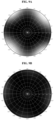
- FIGS. 9A and 9B are graphs illustrating results of experiments on reflectivity of a polarizer.
- FIG. 9A illustrates a result of a simulation experiment on reflectivity of a polarizer including a HWP in which a refractive index anisotropy is absent; and
- FIG. 9B illustrates a result of a simulation experiment on reflectivity of the polarizer 101 according to the first exemplary embodiment.
- a relatively dark portion of FIGS. 9A and 9B indicates a portion in which reflection of external light is effectively prevented, and a relatively bright portion thereof indicates a portion in which relatively low efficiency in preventing reflection of external light is exhibited.
- the polarizer 101 according to the first exemplary embodiment can effectively prevent reflection of external light in all directions irrespective of an incident angle of external light and can be excellent in representing a black color.
- the polarizer 101 according to the first exemplary embodiment can have the HWP 130 having a negative A-plate property, and can prevent reflection of external light irrespective of an incident angle of external light. Accordingly, a product using the polarizer 101 according to the first exemplary embodiment can be excellent in representing a black color and can have an excellent contrast ratio.
- FIG. 4 is an exploded perspective view illustrating a polarizer 102 according to the second exemplary embodiment.
- the polarizer 102 according to the second exemplary embodiment includes a linear polarizer 110, a HWP 130 formed on the linear polarizer 110, and a QWP 120 formed on the HWP 130.
- a configuration of the HWP 130 and the QWP 120 according to the second exemplary embodiment can be the same as that of the first exemplary embodiment.
- FIG. 5 is a cross-sectional view illustrating a polarizer 103 according to the third exemplary embodiment.
- the polarizer 103 can include a linear polarizer 110, a QWP 120, a HWP 130, and a support layer 150 interposed between the linear polarizer 110 and the QWP 120.
- the support layer 150 can serve to support and protect the polarizer 103.
- the support layer 150 can use, for example, a tri-acetyl cellulose (TAC) film.
- TAC film can have excellent durability and mechanical strength.
- the polarizer 103 according to the third exemplary embodiment can further include an adhesive layer 160 formed on the HWP 130.
- the adhesive layer 160 can be formed of an adhesive resin.
- FIG. 6 is a plan view illustrating an OLED display 104 according to the fourth exemplary embodiment.
- FIG. 7 is a cross-sectional view taken along line I-I' of FIG. 6 .
- the OLED display 104 can include a display panel 301 and a polarizer 101.
- the display panel 301 can include a first substrate 311, a wiring unit 330, an OLED 210, and a second substrate 312.
- the first substrate 311 can use an insulating substrate formed of one or more of the following materials: glass, quartz, ceramic, and plastic.
- the fourth exemplary embodiment is not limited thereto, and the first substrate 311 can also use a metallic substrate formed of stainless steel, or the like.
- a buffer layer 321 can be formed on the first substrate 311.
- the buffer layer 321 can include one or more of various inorganic and organic layers.
- the buffer layer 321 can serve to reduce or effectively prevent the infiltration of impure elements such as moisture into the wiring unit 330 or the OLED 210 through the first substrate 311 and can also planarize a surface of the first substrate 311.
- the buffer layer 321 is not necessarily required, and can be omitted.
- the wiring unit 330 can be formed on the buffer layer 321.
- the wiring unit 330 can include a switching thin film transistor (TFT) 10, a driving TFT 20, and a capacitor 80, and can drive the OLED 210.
- the OLED 210 can display an image by emitting light based on a driving signal transmitted from the wiring unit 330.
- FIGS. 6 and 7 illustrate the OLED display 104 as an active matrix organic light emitting diode (AMOLED) display having a 2Tr-1Cap structure in which a single pixel includes two thin film transistors, for example, the switching TFT 10 and the driving TFT 20, and a single capacitor, for example, the capacitor 80.
- AMOLED active matrix organic light emitting diode
- the fourth exemplary embodiment is not limited thereto.
- the OLED display 104 according to the fourth exemplary embodiment can have various structures in which a single pixel includes three or more thin film transistors and two or more capacitors and an additional wiring can further be included.
- the term "pixel" refers to a minimum unit for displaying an image, and the OLED display 104 can display an image through a plurality of pixels.
- the switching TFT 10, the driving TFT 20, the capacitor 80, and the OLED 210 can be included in each pixel.
- a gate line 351, a data line 371 insulated from and intersecting the gate line 351, and a common power line 372 can be formed in the wiring unit 330.
- a single pixel can be defined by a boundary among the gate line 351, the data line 371, and the common power line 372.
- the definition of the pixel is not limited thereto in embodiments of the invention.
- the pixel can be defined by a pixel defining layer (PDL) 391 or a black matrix.
- the OLED 210 can include a first electrode 211, an organic light emitting layer 212 formed on the first electrode 211, and a second electrode 213 formed on the organic light emitting layer 212. A hole and an electron from the first electrode 211 and the second electrode 213, respectively, are injected into the organic light emitting layer 212 to be combined with one another to thereby form an exciton.
- the OLED 210 can emit light by energy generated when the exciton falls from an excited state to a ground state.
- the capacitor 80 can include a pair of capacitor plates 358 and 378, which are formed to have an insulating interlayer 345 therebetween.
- the insulating interlayer 345 can be a dielectric material. Capacitance of the capacitor 80 can be determined by an amount of electric charges stored in the capacitor 80 and a level of a voltage between the capacitor plates 358 and 378.
- the switching TFT 10 can include a switching semiconductor layer 331, a switching gate electrode 352, a switching source electrode 373, and a switching drain electrode 374.
- the driving TFT 20 can include a driving semiconductor layer 332, a driving gate electrode 355, a driving source electrode 376, and a driving drain electrode 377.
- the switching semiconductor layer 331 can be insulated from the switching gate electrode 352 by a gate insulating layer 341, and the driving semiconductor layer 332 can be insulated from the driving gate electrode 355 by the gate insulating layer 341.
- the switching TFT 10 can be used as a switching element that selects a pixel to perform light emission.
- the switching gate electrode 352 can be connected to the gate line 351.
- the switching source electrode 373 can be connected to the data line 371.
- the switching drain electrode 374 can be formed to be spaced apart from the switching source electrode 373 and can be connected to one of the capacitor plates, for example, the capacitor plate 358.
- the driving TFT 20 can apply, to the first electrode 211, a driving power for allowing the organic light emitting layer 212 of the OLED 210 in the pixel selected by the switching TFT 10, to perform light emission.
- the driving gate electrode 355 can be connected to the capacitor plate 358, which is connected to the switching drain electrode 374.
- the driving source electrode 376 and the other capacitor plate 378 can be connected to the common power line 372.
- the driving drain electrode 377 can be connected to the first electrode 211 of the OLED 210 through a contact hole.
- the switching TFT 10 can be operated by a gate voltage applied to the gate line 351 to thereby transmit a data voltage applied to the data line 371 to the driving TFT 20.
- a voltage having a level that is substantially equal to a difference between a level of a data voltage transmitted by (or from) the switching TFT 10 and a level of a common voltage applied from the common power line 372 to the driving TFT 20 can be stored in the capacitor 80.
- a current having a level equivalent to the level of the voltage stored in the capacitor 80 can flow into the OLED 210 through the driving TFT 20 such that the OLED 210 can emit light.
- the first electrode 211 can be an anode that injects holes and the second electrode 213 can be a cathode that injects electrons.
- the fourth exemplary embodiment is not limited thereto, and can be modified such that the first electrode 211 is a cathode and the second electrode 213 is an anode.
- a planarization layer 346 can be formed on the insulating interlayer 345.
- the planarization layer 346 can be formed of an insulating material, and can protect the wiring unit 330.
- the planarization layer 346 and the insulating interlayer 345 can be formed of the same material.
- the driving drain electrode 377 of the driving TFT 20 can be connected to the first electrode 211 of the OLED 210 through the contact hole formed in the planarization layer 346.
- the first electrode 211 can include a reflective layer and the second electrode 213 can include a transflective layer. Accordingly, a light generated in the organic light emitting layer 212 can be transmitted through the second electrode 213 to be emitted.
- the OLED display 104 according to the fourth exemplary embodiment is a top-emission-type display device.
- the reflective layer and the transflective layer can be formed of one or more of the following metals: magnesium (Mg), silver (Ag), gold (Au), calcium (Ca), lithium (Li), chromium (Cr), aluminum (A1), and copper (Cu) or an alloy thereof.
- the type of the layer that is, whether the reflective layer or the transflective layer, can be determined based on a thickness of the layer.
- the transflective layer has a thickness of less than or equal to about 200nm. As the thickness of the transflective layer decreases, a level of light transmittance can increase, and as the thickness of the transflective layer increases, the level of light transmittance can decrease.
- the first electrode 211 can include a reflective layer formed of one or more of the following metals: Mg, Ag, Au, Ca, Li, Cr, Al, and Cu, and a transparent conductive layer formed on the reflective layer.
- the transparent conductive layer can be formed of transparent conductive oxide (TCO), for example, one or more of the following materials: indium tin oxide (ITO), indium zinc oxide (IZO), zinc oxide (ZnO), aluminum zinc oxide (AZO), and indium oxide (In2O3). Since such a transparent conductive layer has a relatively high work function, hole injection through the first electrode 211 can be readily performed.
- the first electrode 211 can have a triple-layer structure in which a transparent conductive layer, a reflective layer, and a transparent conductive layer are sequentially stacked.
- the second electrode 213 can include a transflective layer formed of one or more of the following metals: Mg, Ag, Au, Ca, Li, Cr, Al, and Cu.
- HIL hole injection layer
- HTL hole transporting layer
- ETL electron transporting layer
- EIL electron injection layer
- the organic light emitting layer 212, the HIL, the HTL, the ETL, and the EIL can be referred to as an organic layer.
- Such an organic layer can be formed of a low molecular weight organic material or a polymer organic material.
- the PDL 391 can have an aperture.
- the aperture of the PDL 391 can expose a portion of the first electrode 211.
- the first electrode 211, the organic light emitting layer 212, and the second electrode 213 can be sequentially stacked in the aperture of the PDL 391.
- the second electrode 213 can be formed on the organic light emitting layer 212 and on the PDL 391.
- the PDL 391 can define a light emission area.
- a capping layer can be formed on the second electrode 213.
- the capping layer (not illustrated) can protect the OLED 210.
- the second substrate 312 can be formed on the OLED 210 to be opposite to the first substrate 311.
- the second substrate 312 can be formed of the same material as that forming the first substrate 311.
- the polarizer 101 can be formed on the display panel 301.
- the polarizer 101 according to the fourth exemplary embodiment can have the same configuration as that of the polarizer according to the first exemplary embodiment.
- the polarizer 101 can be formed on the second substrate 312 corresponding to a display surface of the display panel 301.
- the polarizer 101 can be adhered to the second substrate 312 by the adhesive layer 160. Since a description pertaining to the configuration of the polarizer 101 is provided with reference to the first exemplary embodiment, a detailed description thereof will be omitted herein for conciseness.
- FIG. 8 is a cross-sectional view illustrating an OLED display 105 according to the fifth exemplary embodiment.
- the OLED display 105 can include a thin film encapsulation layer 250 formed on an OLED 210.
- the thin film encapsulation layer 250 can include one or more inorganic layers 251, 253, and 255 and one or more organic layers 252 and 254.
- the thin film encapsulation layer 250 can have a structure in which the inorganic layers 251, 253, and 255 and the organic layers 252 and 254 are alternately stacked.
- the inorganic layer 251 can be formed as a lowermost layer of the stacked structure of the thin film encapsulation layer 250.
- the inorganic layer 251 is formed to be most adjacently to the OLED 210.
- FIG. 8 illustrates the thin film encapsulation layer 250 as including the three inorganic layers 251, 253, and 255 and the two organic layers 252 and 254, the fifth exemplary embodiment is not limited thereto.
- the inorganic layers 251, 253, and 255 can be formed of one or more of the following materials: Al 2 O 3 , TiO 2 , ZrO, SiO 2 , AlON, A1N, SiON, Si 3 N 4 , ZnO, and Ta 2 O 5 .
- the inorganic layers 251, 253, and 255 can be formed through a chemical vapor deposition (CVD) process or an atomic layer deposition (ALD) process.
- CVD chemical vapor deposition
- ALD atomic layer deposition
- the fifth exemplary embodiment is not limited thereto, and the inorganic layers 251, 253, and 255 can be formed through various processes known in the pertinent art.
- the organic layers 252 and 254 can be formed of a polymer-based material.
- a polymer-based material can include an acrylic resin, an epoxy resin, polyimide, polyethylene, and the like.
- the organic layers 252 and 254 can be formed through a thermal deposition process.
- the thermal deposition process for forming the organic layers 252 and 254 can be performed within the range of temperature in which the OLED 210 is not damaged.
- the fifth exemplary embodiment is not limited thereto, and the organic layers 252 and 254 can be formed through various processes known in the pertinent art.
- the inorganic layers 251, 253, and 255 formed to have a high density of a thin film can serve to reduce or effectively prevent the infiltration of moisture or oxygen thereinto.
- the infiltration of moisture or oxygen into the OLED 210 can be prevented largely by the inorganic layers 251, 253, and 255.
- Moisture or oxygen passing through the inorganic layers 251, 253, and 255 can be blocked further by the organic layers 252 and 254.
- the organic layers 252 and 254 can exhibit relatively low efficiency in preventing the moisture infiltration, as compared to the inorganic layers 251, 253, and 255.
- the organic layers 252 and 254 can also serve as a buffer layer to reduce stress between respective layers of the inorganic layers 251, 253, and 255 and the organic layers 252 and 254, aside from preventing the moisture infiltration.
- an uppermost surface of the thin film encapsulation layer 250 can be planarized.
- the thin film encapsulation layer 250 can have a thickness of about 10 ⁇ m or less. Accordingly, an overall thickness of the OLED display 105 can be significantly reduced.
- the polarizer 101 can be formed on the thin film encapsulation layer 250.
- the polarizer 101 can use the polarizer according to the first exemplary embodiment.
- a phase retardation layer is provided on the linear polarizer that includes the quarter-wave plate and a half-wave plate. In some embodiments, each of the half-wave and quarter-wave plates is thinner than the linear polarizer.
- the polarizer can include the phase difference plate having refractive index anisotropy, and can effectively prevent reflection of an external light irrespective of an incident angle of the external light.
- the display device can include the polarizer capable of effectively preventing reflection of external light, can be excellent in representing a black color, and can have a high contrast ratio.
Landscapes
- Physics & Mathematics (AREA)
- Optics & Photonics (AREA)
- General Physics & Mathematics (AREA)
- Chemical & Material Sciences (AREA)
- Crystallography & Structural Chemistry (AREA)
- Nonlinear Science (AREA)
- Mathematical Physics (AREA)
- Engineering & Computer Science (AREA)
- Materials Engineering (AREA)
- Polarising Elements (AREA)
- Electroluminescent Light Sources (AREA)
- Liquid Crystal (AREA)
- Fittings On The Vehicle Exterior For Carrying Loads, And Devices For Holding Or Mounting Articles (AREA)
Claims (12)
- Polarisator (101), umfassend:einen linearen Polarisator (110); undeine Phasenverzögerungsschicht (140), die eine Viertelwellenplatte (120) und eine Halbwellenplatte (130) beinhaltet, die in Richtung einer z-Achse geschichtet sind,wobei die Halbwellenplatte eine anisotrope Brechungsindex-Schicht umfasst,wobei die anisotrope Brechungsindex-Schicht einen Brechungsindex Nx, der in Richtung einer x-Achse definiert ist, einen Brechungsindex Ny, der in Richtung einer y-Achse definiert ist, und einen Brechungsindex Nz, der in Richtung der z-Achse definiert ist, aufweist,wobei der lineare Polarisator (110) und die Phasenverzögerungsschicht (140) in Richtung der z-Achse geschichtet sind,wobei Nx = Nz > Ny,wobei die anisotrope Brechungsindex-Schicht eine Flüssigkristallschicht (132) umfasst, umfassend eine diskotische Verbindung (133), undwobei die diskotische Verbindung (133) eine Scheibenoberfläche aufweist, und wobei die Scheibenoberfläche einen Neigungswinkel in dem Bereich von etwa 60 Grad bis etwa 90 Grad in Bezug auf eine Oberfläche der Halbwellenplatte (130) aufweist.
- Polarisator (101) nach Anspruch 1, wobei jeder von Nx und Nz in dem Bereich von etwa 1,6 bis etwa 1,8 ist.
- Polarisator (101) nach einem der Ansprüche 1 bis 2, wobei Ny in dem Bereich von etwa 1,5 bis etwa 1,7 ist.
- Polarisator (101) nach einem der Ansprüche 1 bis 3, wobei die Differenz zwischen Nx und Ny in dem Bereich von etwa 0,05 bis etwa 0,2 ist.
- Polarisator (101) nach einem der Ansprüche 1 bis 4, wobei die anisotrope Brechungsindex-Schicht eine Stärke in dem Bereich von etwa 1 µm bis etwa 5 µm aufweist.
- Polarisator (101) nach einem der Ansprüche 1 bis 5, wobei die anisotrope Brechungsindex-Schicht eine Stärke von "a" µm aufweist und wobei "b" = Nx - Ny ist, wobei 0,1 < a x b < 0,5.
- Polarisator (101) nach einem der Ansprüche 1 bis 6, wobei die Halbwellenplatte (130) eine Ausrichtungsschicht umfasst, und wobei die anisotrope Brechungsindex-Schicht auf der Ausrichtungsschicht ist.
- Polarisator (101) nach einem der Ansprüche 1 bis 7, wobei die Viertelwellenplatte (120) ein cyclisches Olefinpolymer, COP, umfasst.
- Polarisator (101) nach einem der Ansprüche 1 bis 8, wobei die Viertelwellenplatte (120) auf dem linearen Polarisator (110) ist und wobei die Halbwellenplatte (130) auf der Viertelwellenplatte ist; oder
wobei die Halbwellenplatte auf dem linearen Polarisator ist und wobei die Viertelwellenplatte auf der Halbwellenplatte ist. - Polarisator (101) nach einem der Ansprüche 1 bis 9, wobei jede von der Halbwellen- und der Viertelwellenplatte (130, 120) dünner ist als der lineare Polarisator (110).
- Anzeigevorrichtung (104, 105), umfassend:eine Anzeigetafel (301); undeinen Polarisator (101) auf der Anzeigetafel,wobei der Polarisator gemäß einem der Ansprüche 1 bis 10 ist.
- Anzeigevorrichtung (104, 105) nach Anspruch 11, wobei die Anzeigetafel (301) Folgendes umfasst:ein erstes Substrat (311);eine erste Elektrode (211) auf dem ersten Substrat;eine organische lichtemittierende Schicht (212) auf der ersten Elektrode; undeine zweite Elektrode (213) auf der organischen lichtemittierenden Schicht;optional ferner umfassend ein zweites Substrat (312) auf der zweiten Elektrode, wobei der Polarisator (101) auf dem zweiten Substrat ist;optional ferner umfassend eine Dünnfilmverkapselungsschicht (250) auf der zweiten Elektrode, wobei der Polarisator auf der Dünnfilmverkapselungsschicht ist.
Applications Claiming Priority (1)
| Application Number | Priority Date | Filing Date | Title |
|---|---|---|---|
| KR1020150033329A KR102440078B1 (ko) | 2015-03-10 | 2015-03-10 | 편광판 및 이를 포함하는 표시장치 |
Publications (2)
| Publication Number | Publication Date |
|---|---|
| EP3067722A1 EP3067722A1 (de) | 2016-09-14 |
| EP3067722B1 true EP3067722B1 (de) | 2024-10-16 |
Family
ID=55524157
Family Applications (1)
| Application Number | Title | Priority Date | Filing Date |
|---|---|---|---|
| EP16158811.6A Active EP3067722B1 (de) | 2015-03-10 | 2016-03-04 | Polarisator und anzeigevorrichtung damit |
Country Status (4)
| Country | Link |
|---|---|
| US (2) | US9952369B2 (de) |
| EP (1) | EP3067722B1 (de) |
| KR (1) | KR102440078B1 (de) |
| CN (1) | CN105974507B (de) |
Families Citing this family (13)
| Publication number | Priority date | Publication date | Assignee | Title |
|---|---|---|---|---|
| CN105510999B (zh) * | 2016-01-28 | 2019-05-28 | 京东方科技集团股份有限公司 | 减反射结构及其制造方法、显示器及其制造方法 |
| JPWO2018123725A1 (ja) * | 2016-12-26 | 2019-10-31 | 富士フイルム株式会社 | 円偏光板、有機エレクトロルミネッセンス表示装置 |
| CN106856229B (zh) * | 2016-12-28 | 2019-11-26 | 京东方科技集团股份有限公司 | 有机发光二极管及应用其的显示器件 |
| KR102024264B1 (ko) * | 2017-01-25 | 2019-09-23 | 주식회사 엘지화학 | 반사 방지용 광학 필터 및 유기 발광 장치 |
| WO2018194421A1 (ko) | 2017-04-20 | 2018-10-25 | 주식회사 엘지화학 | 반사 방지용 광학 필터 및 유기 발광 장치 |
| CN108565356A (zh) * | 2018-04-26 | 2018-09-21 | 武汉华星光电技术有限公司 | Oled显示装置 |
| US20190334127A1 (en) * | 2018-04-26 | 2019-10-31 | Wuhan China Star Optoelectronics Technology Co., Ltd. | Oled display device |
| US11693165B2 (en) * | 2018-06-11 | 2023-07-04 | Lockheed Martin Corporation | Thin film optics |
| CN110208957A (zh) * | 2019-05-31 | 2019-09-06 | 京东方科技集团股份有限公司 | 有机发光显示面板及电子设备 |
| KR102895160B1 (ko) * | 2019-09-04 | 2025-12-05 | 삼성디스플레이 주식회사 | 표시 장치 |
| KR102686387B1 (ko) * | 2019-11-01 | 2024-07-22 | 삼성디스플레이 주식회사 | 표시 장치 및 표시 장치 제조 방법 |
| CN111415975A (zh) * | 2020-04-30 | 2020-07-14 | 武汉华星光电半导体显示技术有限公司 | 一种显示面板 |
| JP2024010495A (ja) * | 2022-07-12 | 2024-01-24 | 日東電工株式会社 | 円偏光板および画像表示装置 |
Citations (1)
| Publication number | Priority date | Publication date | Assignee | Title |
|---|---|---|---|---|
| US20110001906A1 (en) * | 2008-03-24 | 2011-01-06 | Chang Jun-Won | Polarizing plate with built-in viewing angle compensation film and ips-lcd comprising same |
Family Cites Families (24)
| Publication number | Priority date | Publication date | Assignee | Title |
|---|---|---|---|---|
| JP3854659B2 (ja) * | 1996-04-26 | 2006-12-06 | キヤノン株式会社 | 液晶装置 |
| KR19980070467A (ko) * | 1997-01-17 | 1998-10-26 | 오오자와 슈지로 | 광학필름 |
| TW528895B (en) | 2001-05-29 | 2003-04-21 | Sumitomo Chemical Co | Polarizing conversion plate and projection type liquid crystal display device using the same |
| CN100399075C (zh) * | 2002-04-23 | 2008-07-02 | 日东电工株式会社 | 偏振部件,偏振光源及使用其的图像显示装置 |
| JP2005534993A (ja) | 2002-08-07 | 2005-11-17 | 富士写真フイルム株式会社 | 位相差板および円偏光板 |
| JP2004184809A (ja) * | 2002-12-05 | 2004-07-02 | Nitto Denko Corp | 偏光板の製造方法、偏光板およびそれを用いた画像表示装置 |
| JP4485184B2 (ja) | 2003-12-15 | 2010-06-16 | 株式会社半導体エネルギー研究所 | 発光装置および電子機器 |
| KR100832760B1 (ko) * | 2004-12-22 | 2008-05-27 | 닛토덴코 가부시키가이샤 | 타원 편광판 및 타원 편광판을 사용한 화상 표시 장치 |
| US20080291389A1 (en) * | 2004-12-22 | 2008-11-27 | Nitto Denko Corporation | Elliptically Polarizing Plate and Image Display Apparatus Using the Same |
| KR100835156B1 (ko) * | 2005-03-07 | 2008-06-04 | 닛토덴코 가부시키가이샤 | 액정 패널, 액정 텔레비전 및 액정 표시 장치 |
| KR101157963B1 (ko) | 2005-09-28 | 2012-06-25 | 엘지디스플레이 주식회사 | 액정표시장치 |
| JPWO2007063629A1 (ja) * | 2005-12-02 | 2009-05-07 | シャープ株式会社 | 液晶表示装置 |
| JP2007156085A (ja) * | 2005-12-05 | 2007-06-21 | Toshiba Matsushita Display Technology Co Ltd | 液晶表示装置 |
| WO2007097595A1 (en) | 2006-02-27 | 2007-08-30 | Lg Chem Ltd. | Very thin achromatic quater wave film laminate for transflective lcd and method for producing the same |
| JP2008122851A (ja) * | 2006-11-15 | 2008-05-29 | Nitto Denko Corp | 光学積層体、光学積層体の製造方法、及び光学積層体の用途 |
| US20080309854A1 (en) * | 2007-06-15 | 2008-12-18 | Zhibing Ge | Wide Viewing Angle and Broadband Circular Polarizers for Transflective Liquid Crystal Displays |
| JP2009053684A (ja) * | 2007-07-30 | 2009-03-12 | Fujifilm Corp | 位相差フィルム、偏光板、及びそれを用いた液晶表示装置 |
| US7948592B2 (en) * | 2008-06-23 | 2011-05-24 | Samsung Electronics Co., Ltd. | Display device for increasing viewing angle |
| CN101943824B (zh) * | 2010-08-06 | 2012-05-23 | 信利半导体有限公司 | 一种液晶3d眼镜及3d眼镜显示系统 |
| KR101943378B1 (ko) | 2011-06-29 | 2019-01-30 | 삼성디스플레이 주식회사 | 유기 발광 표시 장치 |
| KR101361722B1 (ko) | 2012-06-05 | 2014-02-13 | 주식회사 엘엠에스 | 위상지연필름, 및 이를 포함하는 입체영상 표시장치 |
| KR101542618B1 (ko) | 2012-12-14 | 2015-08-06 | 제일모직주식회사 | 편광판 및 이를 포함하는 광학 표시 장치 |
| CN103207426B (zh) * | 2013-03-28 | 2015-09-16 | 京东方科技集团股份有限公司 | 一种偏光片及显示装置 |
| US9939974B2 (en) * | 2014-12-29 | 2018-04-10 | Lg Display Co., Ltd. | Contact sensitive display device with thin profile and low external light reflectivity |
-
2015
- 2015-03-10 KR KR1020150033329A patent/KR102440078B1/ko active Active
- 2015-12-03 US US14/958,795 patent/US9952369B2/en active Active
-
2016
- 2016-03-04 EP EP16158811.6A patent/EP3067722B1/de active Active
- 2016-03-08 CN CN201610130217.3A patent/CN105974507B/zh active Active
-
2018
- 2018-03-26 US US15/935,842 patent/US10330842B2/en active Active
Patent Citations (1)
| Publication number | Priority date | Publication date | Assignee | Title |
|---|---|---|---|---|
| US20110001906A1 (en) * | 2008-03-24 | 2011-01-06 | Chang Jun-Won | Polarizing plate with built-in viewing angle compensation film and ips-lcd comprising same |
Also Published As
| Publication number | Publication date |
|---|---|
| KR20160110672A (ko) | 2016-09-22 |
| US20160266296A1 (en) | 2016-09-15 |
| US10330842B2 (en) | 2019-06-25 |
| KR102440078B1 (ko) | 2022-09-06 |
| CN105974507B (zh) | 2021-08-17 |
| EP3067722A1 (de) | 2016-09-14 |
| US20180217310A1 (en) | 2018-08-02 |
| CN105974507A (zh) | 2016-09-28 |
| US9952369B2 (en) | 2018-04-24 |
Similar Documents
| Publication | Publication Date | Title |
|---|---|---|
| US10330842B2 (en) | Polarizer and display device comprising the same | |
| CN110192130B (zh) | 带光学补偿层的偏振片及使用了其的有机el面板 | |
| US9853236B2 (en) | Polarizer and display device comprising the same | |
| TWI835718B (zh) | 光學堆疊體、圓偏光板、觸控面板及影像顯示裝置 | |
| KR102103498B1 (ko) | 보상 필름, 광학 필름 및 표시 장치 | |
| US20150378075A1 (en) | Optical film, manufacturing method thereof, and display device | |
| CN105676318B (zh) | 抗反射膜和包括其的有机发光器件 | |
| US20140159001A1 (en) | Flexible organic light emitting display device | |
| CN110050210A (zh) | 显示装置 | |
| JP2019532338A (ja) | 反射防止用光学フィルタ及び有機発光装置 | |
| CN109844581B (zh) | 用于抗反射的滤光器和有机发光器件 | |
| KR101966336B1 (ko) | 터치패널 및 이를 포함하는 유기발광 표시장치 | |
| KR20200100068A (ko) | 위상차판, 광학 보상층 부착 편광판, 화상 표시 장치, 및 터치 패널 화상 표시 장치 | |
| KR102146533B1 (ko) | 편광판 및 유기발광소자 | |
| KR102060795B1 (ko) | 반사 방지층 및 비침 방지층 부착 편광판 및 그 제조 방법 | |
| WO2019123947A1 (ja) | 位相差フィルム、光学補償層付偏光板、画像表示装置、およびタッチパネル付き画像表示装置 | |
| US20150378076A1 (en) | Optical film, manufacturing method thereof, and display device | |
| KR101950813B1 (ko) | 코팅형 위상차 필름 및 이를 구비한 유기전계발광 표시소자 | |
| JP2020516946A (ja) | 反射防止用光学フィルタ及び有機発光装置 | |
| US11181677B2 (en) | Polarizing film, method for preparing the same, and display device including the same | |
| KR20190098876A (ko) | 편광유닛, 이의 제조방법 및 상기 편광유닛을 포함하는 표시장치 | |
| KR20180050802A (ko) | 유기발광장치 | |
| KR20200124804A (ko) | 표시 장치 | |
| WO2020115977A1 (ja) | 位相差層付偏光板およびそれを用いた画像表示装置 | |
| KR102682281B1 (ko) | 위상차층 부착 편광판 및 이를 이용한 화상 표시 장치 |
Legal Events
| Date | Code | Title | Description |
|---|---|---|---|
| PUAI | Public reference made under article 153(3) epc to a published international application that has entered the european phase |
Free format text: ORIGINAL CODE: 0009012 |
|
| AK | Designated contracting states |
Kind code of ref document: A1 Designated state(s): AL AT BE BG CH CY CZ DE DK EE ES FI FR GB GR HR HU IE IS IT LI LT LU LV MC MK MT NL NO PL PT RO RS SE SI SK SM TR |
|
| AX | Request for extension of the european patent |
Extension state: BA ME |
|
| STAA | Information on the status of an ep patent application or granted ep patent |
Free format text: STATUS: REQUEST FOR EXAMINATION WAS MADE |
|
| 17P | Request for examination filed |
Effective date: 20170112 |
|
| RBV | Designated contracting states (corrected) |
Designated state(s): AL AT BE BG CH CY CZ DE DK EE ES FI FR GB GR HR HU IE IS IT LI LT LU LV MC MK MT NL NO PL PT RO RS SE SI SK SM TR |
|
| STAA | Information on the status of an ep patent application or granted ep patent |
Free format text: STATUS: EXAMINATION IS IN PROGRESS |
|
| 17Q | First examination report despatched |
Effective date: 20180905 |
|
| P01 | Opt-out of the competence of the unified patent court (upc) registered |
Effective date: 20230516 |
|
| GRAP | Despatch of communication of intention to grant a patent |
Free format text: ORIGINAL CODE: EPIDOSNIGR1 |
|
| STAA | Information on the status of an ep patent application or granted ep patent |
Free format text: STATUS: GRANT OF PATENT IS INTENDED |
|
| RIC1 | Information provided on ipc code assigned before grant |
Ipc: H10K 50/86 20230101ALI20240423BHEP Ipc: G02B 27/28 20060101ALI20240423BHEP Ipc: G02B 5/32 20060101ALI20240423BHEP Ipc: G02B 5/30 20060101AFI20240423BHEP |
|
| INTG | Intention to grant announced |
Effective date: 20240508 |
|
| GRAS | Grant fee paid |
Free format text: ORIGINAL CODE: EPIDOSNIGR3 |
|
| GRAA | (expected) grant |
Free format text: ORIGINAL CODE: 0009210 |
|
| STAA | Information on the status of an ep patent application or granted ep patent |
Free format text: STATUS: THE PATENT HAS BEEN GRANTED |
|
| AK | Designated contracting states |
Kind code of ref document: B1 Designated state(s): AL AT BE BG CH CY CZ DE DK EE ES FI FR GB GR HR HU IE IS IT LI LT LU LV MC MK MT NL NO PL PT RO RS SE SI SK SM TR |
|
| REG | Reference to a national code |
Ref country code: GB Ref legal event code: FG4D |
|
| REG | Reference to a national code |
Ref country code: DE Ref legal event code: R096 Ref document number: 602016089835 Country of ref document: DE Ref country code: CH Ref legal event code: EP |
|
| REG | Reference to a national code |
Ref country code: IE Ref legal event code: FG4D |
|
| REG | Reference to a national code |
Ref country code: LT Ref legal event code: MG9D |
|
| REG | Reference to a national code |
Ref country code: NL Ref legal event code: MP Effective date: 20241016 |
|
| REG | Reference to a national code |
Ref country code: AT Ref legal event code: MK05 Ref document number: 1733361 Country of ref document: AT Kind code of ref document: T Effective date: 20241016 |
|
| PG25 | Lapsed in a contracting state [announced via postgrant information from national office to epo] |
Ref country code: NL Free format text: LAPSE BECAUSE OF FAILURE TO SUBMIT A TRANSLATION OF THE DESCRIPTION OR TO PAY THE FEE WITHIN THE PRESCRIBED TIME-LIMIT Effective date: 20241016 |
|
| PG25 | Lapsed in a contracting state [announced via postgrant information from national office to epo] |
Ref country code: NL Free format text: LAPSE BECAUSE OF FAILURE TO SUBMIT A TRANSLATION OF THE DESCRIPTION OR TO PAY THE FEE WITHIN THE PRESCRIBED TIME-LIMIT Effective date: 20241016 |
|
| PG25 | Lapsed in a contracting state [announced via postgrant information from national office to epo] |
Ref country code: IS Free format text: LAPSE BECAUSE OF FAILURE TO SUBMIT A TRANSLATION OF THE DESCRIPTION OR TO PAY THE FEE WITHIN THE PRESCRIBED TIME-LIMIT Effective date: 20250216 Ref country code: HR Free format text: LAPSE BECAUSE OF FAILURE TO SUBMIT A TRANSLATION OF THE DESCRIPTION OR TO PAY THE FEE WITHIN THE PRESCRIBED TIME-LIMIT Effective date: 20241016 Ref country code: PT Free format text: LAPSE BECAUSE OF FAILURE TO SUBMIT A TRANSLATION OF THE DESCRIPTION OR TO PAY THE FEE WITHIN THE PRESCRIBED TIME-LIMIT Effective date: 20250217 |
|
| PG25 | Lapsed in a contracting state [announced via postgrant information from national office to epo] |
Ref country code: FI Free format text: LAPSE BECAUSE OF FAILURE TO SUBMIT A TRANSLATION OF THE DESCRIPTION OR TO PAY THE FEE WITHIN THE PRESCRIBED TIME-LIMIT Effective date: 20241016 |
|
| PG25 | Lapsed in a contracting state [announced via postgrant information from national office to epo] |
Ref country code: BG Free format text: LAPSE BECAUSE OF FAILURE TO SUBMIT A TRANSLATION OF THE DESCRIPTION OR TO PAY THE FEE WITHIN THE PRESCRIBED TIME-LIMIT Effective date: 20241016 |
|
| PG25 | Lapsed in a contracting state [announced via postgrant information from national office to epo] |
Ref country code: ES Free format text: LAPSE BECAUSE OF FAILURE TO SUBMIT A TRANSLATION OF THE DESCRIPTION OR TO PAY THE FEE WITHIN THE PRESCRIBED TIME-LIMIT Effective date: 20241016 |
|
| PG25 | Lapsed in a contracting state [announced via postgrant information from national office to epo] |
Ref country code: NO Free format text: LAPSE BECAUSE OF FAILURE TO SUBMIT A TRANSLATION OF THE DESCRIPTION OR TO PAY THE FEE WITHIN THE PRESCRIBED TIME-LIMIT Effective date: 20250116 |
|
| PG25 | Lapsed in a contracting state [announced via postgrant information from national office to epo] |
Ref country code: LV Free format text: LAPSE BECAUSE OF FAILURE TO SUBMIT A TRANSLATION OF THE DESCRIPTION OR TO PAY THE FEE WITHIN THE PRESCRIBED TIME-LIMIT Effective date: 20241016 Ref country code: AT Free format text: LAPSE BECAUSE OF FAILURE TO SUBMIT A TRANSLATION OF THE DESCRIPTION OR TO PAY THE FEE WITHIN THE PRESCRIBED TIME-LIMIT Effective date: 20241016 Ref country code: GR Free format text: LAPSE BECAUSE OF FAILURE TO SUBMIT A TRANSLATION OF THE DESCRIPTION OR TO PAY THE FEE WITHIN THE PRESCRIBED TIME-LIMIT Effective date: 20250117 |
|
| PG25 | Lapsed in a contracting state [announced via postgrant information from national office to epo] |
Ref country code: PL Free format text: LAPSE BECAUSE OF FAILURE TO SUBMIT A TRANSLATION OF THE DESCRIPTION OR TO PAY THE FEE WITHIN THE PRESCRIBED TIME-LIMIT Effective date: 20241016 |
|
| PG25 | Lapsed in a contracting state [announced via postgrant information from national office to epo] |
Ref country code: RS Free format text: LAPSE BECAUSE OF FAILURE TO SUBMIT A TRANSLATION OF THE DESCRIPTION OR TO PAY THE FEE WITHIN THE PRESCRIBED TIME-LIMIT Effective date: 20250116 |
|
| PG25 | Lapsed in a contracting state [announced via postgrant information from national office to epo] |
Ref country code: SM Free format text: LAPSE BECAUSE OF FAILURE TO SUBMIT A TRANSLATION OF THE DESCRIPTION OR TO PAY THE FEE WITHIN THE PRESCRIBED TIME-LIMIT Effective date: 20241016 |
|
| PG25 | Lapsed in a contracting state [announced via postgrant information from national office to epo] |
Ref country code: DK Free format text: LAPSE BECAUSE OF FAILURE TO SUBMIT A TRANSLATION OF THE DESCRIPTION OR TO PAY THE FEE WITHIN THE PRESCRIBED TIME-LIMIT Effective date: 20241016 |
|
| REG | Reference to a national code |
Ref country code: DE Ref legal event code: R097 Ref document number: 602016089835 Country of ref document: DE |
|
| PG25 | Lapsed in a contracting state [announced via postgrant information from national office to epo] |
Ref country code: EE Free format text: LAPSE BECAUSE OF FAILURE TO SUBMIT A TRANSLATION OF THE DESCRIPTION OR TO PAY THE FEE WITHIN THE PRESCRIBED TIME-LIMIT Effective date: 20241016 |
|
| PG25 | Lapsed in a contracting state [announced via postgrant information from national office to epo] |
Ref country code: RO Free format text: LAPSE BECAUSE OF FAILURE TO SUBMIT A TRANSLATION OF THE DESCRIPTION OR TO PAY THE FEE WITHIN THE PRESCRIBED TIME-LIMIT Effective date: 20241016 |
|
| PG25 | Lapsed in a contracting state [announced via postgrant information from national office to epo] |
Ref country code: SK Free format text: LAPSE BECAUSE OF FAILURE TO SUBMIT A TRANSLATION OF THE DESCRIPTION OR TO PAY THE FEE WITHIN THE PRESCRIBED TIME-LIMIT Effective date: 20241016 |
|
| PG25 | Lapsed in a contracting state [announced via postgrant information from national office to epo] |
Ref country code: CZ Free format text: LAPSE BECAUSE OF FAILURE TO SUBMIT A TRANSLATION OF THE DESCRIPTION OR TO PAY THE FEE WITHIN THE PRESCRIBED TIME-LIMIT Effective date: 20241016 |
|
| PG25 | Lapsed in a contracting state [announced via postgrant information from national office to epo] |
Ref country code: IT Free format text: LAPSE BECAUSE OF FAILURE TO SUBMIT A TRANSLATION OF THE DESCRIPTION OR TO PAY THE FEE WITHIN THE PRESCRIBED TIME-LIMIT Effective date: 20241016 |
|
| PLBE | No opposition filed within time limit |
Free format text: ORIGINAL CODE: 0009261 |
|
| STAA | Information on the status of an ep patent application or granted ep patent |
Free format text: STATUS: NO OPPOSITION FILED WITHIN TIME LIMIT |
|
| PG25 | Lapsed in a contracting state [announced via postgrant information from national office to epo] |
Ref country code: SE Free format text: LAPSE BECAUSE OF FAILURE TO SUBMIT A TRANSLATION OF THE DESCRIPTION OR TO PAY THE FEE WITHIN THE PRESCRIBED TIME-LIMIT Effective date: 20241016 |
|
| 26N | No opposition filed |
Effective date: 20250717 |
|
| PG25 | Lapsed in a contracting state [announced via postgrant information from national office to epo] |
Ref country code: MC Free format text: LAPSE BECAUSE OF FAILURE TO SUBMIT A TRANSLATION OF THE DESCRIPTION OR TO PAY THE FEE WITHIN THE PRESCRIBED TIME-LIMIT Effective date: 20241016 |
|
| REG | Reference to a national code |
Ref country code: CH Ref legal event code: H13 Free format text: ST27 STATUS EVENT CODE: U-0-0-H10-H13 (AS PROVIDED BY THE NATIONAL OFFICE) Effective date: 20251024 |
|
| PG25 | Lapsed in a contracting state [announced via postgrant information from national office to epo] |
Ref country code: LU Free format text: LAPSE BECAUSE OF NON-PAYMENT OF DUE FEES Effective date: 20250304 |
|
| REG | Reference to a national code |
Ref country code: BE Ref legal event code: MM Effective date: 20250331 |
|
| PG25 | Lapsed in a contracting state [announced via postgrant information from national office to epo] |
Ref country code: BE Free format text: LAPSE BECAUSE OF NON-PAYMENT OF DUE FEES Effective date: 20250331 |
|
| PG25 | Lapsed in a contracting state [announced via postgrant information from national office to epo] |
Ref country code: CH Free format text: LAPSE BECAUSE OF NON-PAYMENT OF DUE FEES Effective date: 20250331 |
|
| PG25 | Lapsed in a contracting state [announced via postgrant information from national office to epo] |
Ref country code: IE Free format text: LAPSE BECAUSE OF NON-PAYMENT OF DUE FEES Effective date: 20250304 |
|
| PGFP | Annual fee paid to national office [announced via postgrant information from national office to epo] |
Ref country code: GB Payment date: 20260224 Year of fee payment: 11 |
|
| PGFP | Annual fee paid to national office [announced via postgrant information from national office to epo] |
Ref country code: DE Payment date: 20260220 Year of fee payment: 11 |
|
| PGFP | Annual fee paid to national office [announced via postgrant information from national office to epo] |
Ref country code: FR Payment date: 20260224 Year of fee payment: 11 |