EP3048644B1 - Chip-paket und herstellungsverfahren dafür - Google Patents
Chip-paket und herstellungsverfahren dafür Download PDFInfo
- Publication number
- EP3048644B1 EP3048644B1 EP15167945.3A EP15167945A EP3048644B1 EP 3048644 B1 EP3048644 B1 EP 3048644B1 EP 15167945 A EP15167945 A EP 15167945A EP 3048644 B1 EP3048644 B1 EP 3048644B1
- Authority
- EP
- European Patent Office
- Prior art keywords
- layer
- conductive
- dielectric
- passive component
- circuit
- Prior art date
- Legal status (The legal status is an assumption and is not a legal conclusion. Google has not performed a legal analysis and makes no representation as to the accuracy of the status listed.)
- Active
Links
Images







Classifications
-
- H—ELECTRICITY
- H10—SEMICONDUCTOR DEVICES; ELECTRIC SOLID-STATE DEVICES NOT OTHERWISE PROVIDED FOR
- H10W—GENERIC PACKAGES, INTERCONNECTIONS, CONNECTORS OR OTHER CONSTRUCTIONAL DETAILS OF DEVICES COVERED BY CLASS H10
- H10W70/00—Package substrates; Interposers; Redistribution layers [RDL]
- H10W70/60—Insulating or insulated package substrates; Interposers; Redistribution layers
- H10W70/67—Insulating or insulated package substrates; Interposers; Redistribution layers characterised by their insulating layers or insulating parts
- H10W70/68—Shapes or dispositions thereof
- H10W70/685—Shapes or dispositions thereof comprising multiple insulating layers
-
- H—ELECTRICITY
- H10—SEMICONDUCTOR DEVICES; ELECTRIC SOLID-STATE DEVICES NOT OTHERWISE PROVIDED FOR
- H10W—GENERIC PACKAGES, INTERCONNECTIONS, CONNECTORS OR OTHER CONSTRUCTIONAL DETAILS OF DEVICES COVERED BY CLASS H10
- H10W70/00—Package substrates; Interposers; Redistribution layers [RDL]
- H10W70/60—Insulating or insulated package substrates; Interposers; Redistribution layers
- H10W70/62—Insulating or insulated package substrates; Interposers; Redistribution layers characterised by their interconnections
- H10W70/63—Vias, e.g. via plugs
- H10W70/635—Through-vias
-
- H—ELECTRICITY
- H10—SEMICONDUCTOR DEVICES; ELECTRIC SOLID-STATE DEVICES NOT OTHERWISE PROVIDED FOR
- H10W—GENERIC PACKAGES, INTERCONNECTIONS, CONNECTORS OR OTHER CONSTRUCTIONAL DETAILS OF DEVICES COVERED BY CLASS H10
- H10W70/00—Package substrates; Interposers; Redistribution layers [RDL]
- H10W70/60—Insulating or insulated package substrates; Interposers; Redistribution layers
- H10W70/611—Insulating or insulated package substrates; Interposers; Redistribution layers for connecting multiple chips together
-
- H—ELECTRICITY
- H10—SEMICONDUCTOR DEVICES; ELECTRIC SOLID-STATE DEVICES NOT OTHERWISE PROVIDED FOR
- H10W—GENERIC PACKAGES, INTERCONNECTIONS, CONNECTORS OR OTHER CONSTRUCTIONAL DETAILS OF DEVICES COVERED BY CLASS H10
- H10W72/00—Interconnections or connectors in packages
-
- H—ELECTRICITY
- H05—ELECTRIC TECHNIQUES NOT OTHERWISE PROVIDED FOR
- H05K—PRINTED CIRCUITS; CASINGS OR CONSTRUCTIONAL DETAILS OF ELECTRIC APPARATUS; MANUFACTURE OF ASSEMBLAGES OF ELECTRICAL COMPONENTS
- H05K1/00—Printed circuits
- H05K1/18—Printed circuits structurally associated with non-printed electric components
- H05K1/182—Printed circuits structurally associated with non-printed electric components associated with components mounted in printed circuit boards [PCB], e.g. insert-mounted components [IMC]
- H05K1/185—Printed circuits structurally associated with non-printed electric components associated with components mounted in printed circuit boards [PCB], e.g. insert-mounted components [IMC] associated with components encapsulated in the insulating substrate of the PCBs; associated with components incorporated in internal layers of multilayer circuit boards
-
- H—ELECTRICITY
- H05—ELECTRIC TECHNIQUES NOT OTHERWISE PROVIDED FOR
- H05K—PRINTED CIRCUITS; CASINGS OR CONSTRUCTIONAL DETAILS OF ELECTRIC APPARATUS; MANUFACTURE OF ASSEMBLAGES OF ELECTRICAL COMPONENTS
- H05K3/00—Apparatus or processes for manufacturing printed circuits
- H05K3/10—Apparatus or processes for manufacturing printed circuits in which conductive material is applied to the insulating support in such a manner as to form the desired conductive pattern
- H05K3/20—Apparatus or processes for manufacturing printed circuits in which conductive material is applied to the insulating support in such a manner as to form the desired conductive pattern by affixing prefabricated conductor pattern
- H05K3/205—Apparatus or processes for manufacturing printed circuits in which conductive material is applied to the insulating support in such a manner as to form the desired conductive pattern by affixing prefabricated conductor pattern using a pattern electroplated or electroformed on a metallic carrier
-
- H—ELECTRICITY
- H10—SEMICONDUCTOR DEVICES; ELECTRIC SOLID-STATE DEVICES NOT OTHERWISE PROVIDED FOR
- H10W—GENERIC PACKAGES, INTERCONNECTIONS, CONNECTORS OR OTHER CONSTRUCTIONAL DETAILS OF DEVICES COVERED BY CLASS H10
- H10W74/00—Encapsulations, e.g. protective coatings
-
- H—ELECTRICITY
- H10—SEMICONDUCTOR DEVICES; ELECTRIC SOLID-STATE DEVICES NOT OTHERWISE PROVIDED FOR
- H10W—GENERIC PACKAGES, INTERCONNECTIONS, CONNECTORS OR OTHER CONSTRUCTIONAL DETAILS OF DEVICES COVERED BY CLASS H10
- H10W90/00—Package configurations
- H10W90/701—Package configurations characterised by the relative positions of pads or connectors relative to package parts
- H10W90/721—Package configurations characterised by the relative positions of pads or connectors relative to package parts of bump connectors
- H10W90/724—Package configurations characterised by the relative positions of pads or connectors relative to package parts of bump connectors between a chip and a stacked insulating package substrate, interposer or RDL
Definitions
- the present invention relates to a package substrate, and in particular relates to a package substrate with a passive component embedded therein and manufacturing methods thereof and a chip package having the package substrate.
- the package substrate uses a core layer to support chips thereon.
- the core layer is very expensive. Therefore, methods for lowering the manufacturing cost of chip packages are required.
- An embodiment of the invention provides a package substrate which includes: a dielectric layer; a passive component embedded in the dielectric layer and contacting the dielectric layer; and a circuit layer embedded in the dielectric layer and having a first surface aligned with a second surface of the dielectric layer.
- An embodiment of the invention provides a chip package, which includes: a package substrate including: a dielectric layer; a passive component embedded in the dielectric layer and contacting the dielectric layer; a first circuit layer embedded in the dielectric layer and having a first surface aligned with a second surface of the dielectric layer; and a chip disposed on the package substrate and electrically connected to the first circuit layer and the passive component.
- An embodiment of the invention provides a manufacturing method of a package substrate, which includes: forming a first circuit layer on a carrier; disposing a passive component on the carrier; forming a dielectric layer on the carrier to embed the passive component and the circuit layer in the dielectric layer; forming a second circuit layer on the dielectric layer; and removing the carrier.
- first layer “on,” “overlying,” (and like descriptions) a second layer include embodiments where the first and second layers are in direct contact and those where one or more layers are interposing the first and second layers.
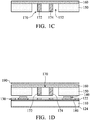
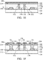
- Figs. 1A-1I are cross-sectional views showing the steps of forming a chip package in accordance with an embodiment of the present invention.
- a carrier 110 is provided, and the carrier 110 has two opposite surfaces 112 and 114.
- the carrier 110 includes resin, polytetrafluoroethene or other materials suitable for support of electronic components.
- conductive layers 122 and 124 are formed on the surfaces 112 and 114, respectively.
- a circuit layer 130 is formed on the conductive layer 122 by, for example, performing an electroplating process, a photolithography process and an etching process.
- a conductive layer 140 is formed on a portion of the circuit layer 130 whereon conductive vias will be formed in subsequent processes.
- the conductive layer 140 is formed by, for example, performing an electroplating process, a photolithography process and an etching process.
- the conductive layers 122 and 124, the circuit layer 130 and the conductive layer 140 include copper or other suitable conductive materials.
- a first dielectric material layer 150 and an adhesive layer 160 are provided.
- the adhesive layer 160 is disposed on the first dielectric material layer 150.
- the first dielectric material layer 150 has a cavity 152 exposing a portion of the adhesive layer 160.
- the first dielectric material layer 150 includes resin or other suitable dielectric materials.
- the adhesive layer 160 includes epoxy or other suitable adhesive materials.
- a passive component 170 is disposed in the cavity 152 to be adhered on the adhesive layer 160.
- the passive component 170 includes a capacitor, an inductor, a resistor or other suitable passive components.
- the passive component 170 is a capacitor, and the passive component 170 has electrode pads 172 and 174 disposed at two opposite ends thereof, respectively.
- a second dielectric material layer 180 is formed on the conductive layer 122 and is adjacent to the circuit layer 130. Specifically, the circuit layer 130 is embedded in the second dielectric material layer 180. The second dielectric material layer 180 has the same material as the first dielectric material layer 150. Then, a conductive layer 190, the adhesive layer 160, the first dielectric material layer 150 and the passive component 170 are stacked on the carrier 110.
- the conductive layer 190 includes copper or other suitable conductive materials.
- a lamination process is performed to combine the first dielectric material layer 150 with the second dielectric material layer 180 so as to form a dielectric layer 210.
- the dielectric layer 210 is, for example, an integral layer includes the same material as the first dielectric material layer 150 (or the second dielectric material layer 180).
- the dielectric layer 210 fills the gaps between the passive component 170, the first dielectric material layer 150, the second dielectric material layer 180, the circuit layer 130 and the conductive layer 140 (as shown in Fig. 1D ).
- the passive component 170, the circuit layer 130 and the conductive layer 140 are embedded in the dielectric layer 210.
- the passive component 170, the circuit layer 130 and the conductive layer 140 are in direct contact with the dielectric layer 210. Since the dielectric layer 210 and the circuit layer 130 are both formed on a surface S of the conductive layer 122, a surface 212 of the dielectric layer 210 is aligned with a surface 132 of the circuit layer 130.
- the adhesive layer 160 is disposed on a surface 214 of the dielectric layer 210, and the surface 214 is opposite to the surface 212. Furthermore, the conductive layer 190 is adhered onto the adhesive layer 160.
- holes T1 and T2 are formed by, for example, a laser drilling process.
- the holes T1 pass through the conductive layer 190, the adhesive layer 160 and the dielectric layer 210.
- the holes T2 pass through the conductive layer 190 and the adhesive layer 160.
- a conductive layer (not shown) is formed on the conductive layer 190 by, for example, an electroplating process, and the conductive layer fills the holes T1 and T2 to form conductive vias V1, V2 and V3. It should be noted that the aspect ratio of the holes T1 is reduced by the conductive layer 140, which helps the conductive layer to fill the holes T1.
- the conductive layer 190 and the conductive layer formed thereon are patterned to form circuit layers 190a and 220 on the surface 214 of the dielectric layer 210.
- the patterning process includes, for example, a photolithography process and an etching process.
- Each of the conductive vias V1 passes through the circuit layer 190a, the adhesive layer 160 and the dielectric layer 210 and is electrically connected to the circuit layers 190a and 220, the conductive layer 140 and the circuit layer 130.
- the conductive via V2 passes through the circuit layer 190a and the adhesive layer 160 and is electrically connected to the circuit layers 190a and 220 and the electrode pad 172 of the passive component 170.
- the conductive via V3 passes through the circuit layer 190a and the adhesive layer 160 and is electrically connected to the circuit layers 190a and 220 and the electrode pad 174 of the passive component 170.
- the manufacturing processes performed on the conductive layer 122 are also performed on the conductive layer 124 to form the same structure as that formed on the conductive layer 122. Therefore, the carrier 110 may be used to fabricate (or support) two package substrates simultaneously.
- the carrier 110 and the conductive layer 124 are removed. Holes T3 are formed to pass through the conductive layer 122, the circuit layer 130 and the dielectric layer 210 by, for example, a laser drilling process. Then, a conductive layer 230 is formed on the conductive layer 122 by, for example, an electroplating process, and the conductive layer 230 fills the holes T3 to form conductive vias V4 and V5. As shown in Fig. 1H , the conductive layers 122 and 230 are patterned to form circuit layers 122a and 230a. In this step, a package substrate 100 is substantially formed.
- the package substrate 100 is flipped up.
- a chip 240 is bonded onto the circuit layer 230a via conductive bumps 242 formed under the chip 240.
- the chip 240 is electrically connected to the passive component 170 through the circuit layer 230a and the conductive vias V4 and V5.
- the chip 240 is located on the surface 212 of the dielectric layer 210.
- a molding process is optionally performed to form an encapsulating layer 250 on the package substrate 100 and covering (or encapsulating) the chip 240.
- the encapsulating layer 250 includes epoxy, acrylate, urethane acrylate or other suitable encapsulating materials.
- Solder balls (or conductive bumps) 260 are formed on the circuit layer 220.
- the solder balls include tin or other suitable solder materials.
- a chip package 100A of the present embodiment is substantially formed.
- a lamination process is performed to embed the passive component 170 into the dielectric layer 210 so as to form the package substrate 100, and therefore the package substrate 100 of the present embodiment does not need to use a core layer. Therefore, the present embodiment may reduce the manufacturing cost of package substrates and chip packages.
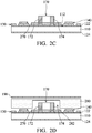
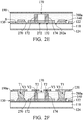
- Figs. 2A-2I are cross-sectional views showing the steps of forming a chip package in accordance with an embodiment of the present invention. It should be noted that some of the elements of Figs. 2A-2I are the same as or similar to those of Figs. 1A-1I , and therefore same or similar reference numbers are used to designate same or similar elements. A detailed description of elements that are the same or similar to those in Figs. 1A-1I is not repeated herein.
- a carrier 110 As shown in Fig. 2A , a carrier 110, conductive layers 122 and 124, a circuit layer 130 and a conductive layer 140 are provided.
- the conductive layer 122, the circuit layer 130 and the conductive layer 140 are stacked on a surface 112 of the carrier 110 sequentially.
- the conductive layer 124 is disposed on a surface 114 of the carrier 110.
- an adhesive layer 270 is formed on the conductive layer 122 by, for example, a printing process or a dispensing process.
- the adhesive layer 270 includes insulating materials, such as epoxy or other suitable adhesive materials.
- a passive component 170 is disposed on the adhesive layer 270 to be adhered on the carrier 110.
- the passive component 170 has electrode pads 172 and 174 disposed at two opposite ends thereof, respectively.
- a conductive layer 190 and a dielectric material layer 280 are stacked on the carrier 110.
- the dielectric material layer 280 has a cavity 282 facing the passive component 170.
- the dielectric material layer 280 includes resin or other suitable dielectric materials.
- a lamination process is performed to melt the dielectric material layer 280 so as to form a dielectric layer 280a.
- the dielectric layer 280a fills the gaps between the passive component 170, the dielectric material layer 280, the circuit layer 130, the conductive layer 140 and the adhesive layer 270 (as shown in Fig. 2D ). Therefore, the passive component 170, the circuit layer 130, the conductive layer 140 and the adhesive layer 270 are embedded in the dielectric layer 280a.
- the passive component 170, the circuit layer 130, the conductive layer 140 and the adhesive layer 270 are in direct contact with the dielectric layer 280a. Since the dielectric layer 280a, the adhesive layer 270 and the circuit layer 130 are formed on a surface S of the conductive layer 122, a surface 282a of the dielectric layer 280a, a surface 272 of the adhesive layer 270 and a surface 132 of the circuit layer 130 are aligned with each other. Furthermore, the conductive layer 190 is pressed onto the dielectric layer 280a.
- holes T1 and T2 are formed by, for example, a laser drilling process.
- the holes T1 and T2 pass through the conductive layer 190 and the dielectric layer 280a.
- a conductive layer (not shown) is formed on the conductive layer 190 by, for example, an electroplating process, and the conductive layer fills the holes T1 and T2 to form conductive vias V1, V2 and V3.
- the conductive layer 190 and the conductive layer formed thereon are patterned to form circuit layers 190a and 220.
- the patterning process includes, for example, a photolithography process and an etching process.
- Each of the conductive vias V1 passes through the circuit layer 190a and the dielectric layer 280a and is electrically connected to the circuit layers 190a and 220, the conductive layer 140 and the circuit layer 130.
- the conductive via V2 passes through the circuit layer 190a and the dielectric layer 280a and is electrically connected to the circuit layers 190a and 220 and the electrode pad 172 of the passive component 170.
- the conductive via V3 passes through the circuit layer 190a and the dielectric layer 280a and is electrically connected to the circuit layers 190a and 220 and the electrode pad 174 of the passive component 170.
- a carrier 110 and the conductive layer 124 are removed. Holes T3 are formed to pass through the conductive layer 122, the circuit layer 130 and the adhesive layer 270 by, for example, a laser drilling process. Then, a conductive layer 230 is formed on the conductive layer 122 by, for example, an electroplating process, and the conductive layer 230 fills the holes T3 to form conductive vias V4 and V5. As shown in Fig. 2H , the conductive layers 122 and 230 are patterned to form circuit layers 122a and 230a. In this step, a package substrate 200 is substantially formed.
- the package substrate 200 is flipped up.
- a chip 240 is bonded onto the circuit layer 230a via conductive bumps 242 formed under the chip 240.
- the chip 240 is electrically connected to the passive component 170 through the circuit layer 230a and the conductive vias V4 and V5.
- a molding process is optionally performed to form an encapsulating layer 250 on the package substrate 200 and covering (or encapsulating) the chip 240.
- Solder balls (or conductive bumps) 260 are formed on the circuit layer 220.
- a chip package 200A of the present embodiment is substantially formed.
- Figs. 3A-3I are cross-sectional views showing the steps of forming a chip package in accordance with an embodiment of the present invention. It should be noted that some of the elements of Figs. 3A-3I are the same as or similar to those of Figs. 1A-1I and Figs. 2A-2I , and therefore same or similar reference numbers are used to designate same or similar elements. A detailed description of elements that are the same or similar to those in Figs. 1A-1I and Figs. 2A-2I is not repeated herein.
- a carrier 110, conductive layer 122, a circuit layer 130 and conductive pillars 310 are provided.
- the conductive layer 122, the circuit layer 130 and the conductive pillars 310 are stacked on a surface 112 of the carrier 110 sequentially.
- the conductive pillars 310 are disposed on the circuit layer 130 and are configured to be conductive vias of a chip package subsequently formed.
- the conductive pillars 310 include copper or other suitable conductive materials.
- the conductive pillars 310 are formed by, for example, an electroplating process.
- an adhesive layer 270 is formed on the conductive layer 122 by, for example, a printing process or a dispensing process.
- the adhesive layer 270 includes epoxy or other suitable adhesive materials.
- a passive component 170 is disposed on the adhesive layer 270 to be adhered on the carrier 110.
- the passive component 170 has electrode pads 172 and 174 disposed at two opposite ends thereof, respectively.
- a pre-molding process is performed to form a dielectric layer 320 on the conductive layer 122 (or the carrier 110) so as to cover the passive component 170, the circuit layer 130 and the adhesive layer 270.
- the dielectric layer 320 includes epoxy, acrylate, urethane acrylate or other suitable encapsulating materials.
- the passive component 170, the circuit layer 130, the conductive pillars 310 and the adhesive layer 270 are embedded in the dielectric layer 320. In one embodiment, the passive component 170, the circuit layer 130, the conductive pillars 310 and the adhesive layer 270 are in direct contact with the dielectric layer 320.
- the dielectric layer 320, the adhesive layer 270 and the circuit layer 130 are formed on a surface S of the conductive layer 122, a surface 324 of the dielectric layer 320, a surface 272 of the adhesive layer 270 and a surface 132 of the circuit layer 130 are aligned with each other.
- the dielectric layer 320 covers top surfaces 312 of the conductive pillars 310, and therefore a grinding process is performed to remove the portion of the dielectric layer 320 covering the top surfaces 312 so as to expose the top surfaces 312.
- holes T2 are formed to pass through the dielectric layer 320.
- an electroless plating process is performed to form a seed layer 330 on a surface 322 of the dielectric layer 320 and sidewalls of the holes T2.
- the seed layer 330 includes copper or other suitable conductive materials.
- a conductive layer 220 is formed on the seed layer 330 by, for example, an electroplating process. The conductive layer 220 fills the holes T2 to form conductive vias V2 and V3.
- the seed layer 330 and the conductive layer 220 are patterned to form a circuit layer 220a.
- the patterning process includes, for example, a photolithography process and an etching process.
- the circuit layer 220a is electrically connected to the conductive pillars 310.
- the conductive via V2 passes through the dielectric layer 320 and is electrically connected to the circuit layer 220a and the electrode pad 172 of the passive component 170.
- the conductive via V3 passes through the dielectric layer 320 and is electrically connected to the circuit layer 220a and the electrode pad 174 of the passive component 170.
- a carrier 110 is removed. Holes T3 are formed to pass through the conductive layer 122, the circuit layer 130 and the adhesive layer 270 by, for example, a laser drilling process. Then, a conductive layer 230 is formed on the conductive layer 122 by, for example, an electroplating process, and the conductive layer 230 fills the holes T3 to form conductive vias V4 and V5. As shown in Fig. 3H , the conductive layers 122 and 230 are patterned to form circuit layers 122a and 230a. In this step, a package substrate 300 is substantially formed.
- the package substrate 300 is flipped up.
- a chip 240 is bonded onto the circuit layer 230a via conductive bumps 242 formed under the chip 240.
- the chip 240 is electrically connected to the passive component 170 through the circuit layer 230a and the conductive vias V4 and V5.
- a molding process is optionally performed to form an encapsulating layer 250 on the package substrate 300 and covering (or encapsulating) the chip 240.
- the encapsulating layer 250 includes epoxy, acrylate, urethane acrylate or other suitable encapsulating materials.
- the encapsulating layer 250 and the dielectric layer 320 have the same material.
- Solder balls (or conductive bumps) 260 are formed on the circuit layer 220a. In this step, a chip package 300A of the present embodiment is substantially formed.
- a pre-molding process is performed to embed the passive component 170 into the dielectric layer 320 so as to form the package substrate 300, and therefore the package substrate 300 of the present embodiment does not need to use a core layer. Therefore, the present embodiment may reduce the manufacturing cost of package substrates and chip packages.
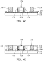
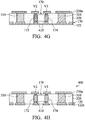
- Figs. 4A-4I are cross-sectional views showing the steps of forming a chip package in accordance with an embodiment of the present invention. It should be noted that some of the elements of Figs. 4A-4I are the same as or similar to those of Figs. 1A-1I , Figs. 2A-2I and Figs. 3A-3I , and therefore same or similar reference numbers are used to designate same or similar elements. A detailed description of elements that are the same or similar to those in Figs. 1A-1I , Figs. 2A-2I and Figs. 3A-3I is not repeated herein.
- a carrier 110, conductive layer 122, a circuit layer 130 and conductive pillars 310 are provided.
- the conductive layer 122, the circuit layer 130 and the conductive pillars 310 are stacked on a surface 112 of the carrier 110 sequentially.
- the conductive pillars 310 are disposed on the circuit layer 130 and are configured to be conductive vias of a chip package subsequently formed.
- the conductive pillars 310 include copper or other suitable conductive materials.
- the conductive pillars 310 are formed by, for example, an electroplating process.
- an adhesive layer 410 is formed on the circuit layer 130 by, for example, a printing process.
- the adhesive layer 410 includes a solder paste including tin (Sn) or other suitable conductive materials.
- a passive component 170 is disposed on the adhesive layer 410 to be adhered on the carrier 110 (or the circuit layer 130).
- a reflow process is performed to help the adhesive layer 410 to adhere to the passive component 170 and the circuit layer 130.
- the passive component 170 has electrode pads 172 and 174 disposed at two opposite ends thereof, respectively. The electrode pads 172 and 174 are connected to the adhesive layer 410, respectively.
- a pre-molding process is performed to form a dielectric layer 320 on the conductive layer 122 (or the carrier 110) so as to cover the passive component 170, the circuit layer 130 and the adhesive layer 410.
- the passive component 170, the circuit layer 130, the conductive pillars 310 and the adhesive layer 410 are embedded in the dielectric layer 320.
- the passive component 170, the circuit layer 130, the conductive pillars 310 and the adhesive layer 410 are in direct contact with the dielectric layer 320.
- the dielectric layer 320 covers top surfaces 312 of the conductive pillars 310, and therefore a grinding process is performed to remove the portion of the dielectric layer 320 covering the top surfaces 312 so as to expose the top surfaces 312.
- holes T2 are formed to pass through the dielectric layer 320.
- an electroless plating process is performed to form a seed layer 330 on a surface 322 of the dielectric layer 320 and sidewalls of the holes T2.
- the seed layer 330 includes copper or other suitable conductive materials.
- a conductive layer 220 is formed on the seed layer 330 by, for example, an electroplating process. The conductive layer 220 fills the holes T2 to form conductive vias V2 and V3.
- the seed layer 330 and the conductive layer 220 are patterned to form a circuit layer 220a.
- the patterning process includes, for example, a photolithography process and an etching process.
- the circuit layer 220a is electrically connected to the conductive pillars 310.
- the conductive via V2 passes through the dielectric layer 320 and is electrically connected to the circuit layer 220a and the electrode pad 172 of the passive component 170.
- the conductive via V3 passes through the dielectric layer 320 and is electrically connected to the circuit layer 220a and the electrode pad 174 of the passive component 170.
- a package substrate 400 is substantially formed.
- the package substrate 400 is flipped up.
- a chip 240 is bonded onto the circuit layer 230a via conductive bumps 242 formed under the chip 240.
- the chip 240 is electrically connected to the passive component 170 through the circuit layer 230a and 122a and the adhesive layer 410.
- a molding process is optionally performed to form an encapsulating layer 250 on the package substrate 400 and covering (or encapsulating) the chip 240.
- Solder balls (or conductive bumps) 260 are formed on the circuit layer 220a.
- a chip package 400A of the present embodiment is substantially formed.
- a lamination process or a pre-molding process is performed to embed a passive component into a dielectric layer so as to form a package substrate, and therefore the package substrate of the present invention does not need to use a core layer. Therefore, the present invention may reduce the manufacturing cost of package substrates and chip packages.
Landscapes
- Engineering & Computer Science (AREA)
- Production Of Multi-Layered Print Wiring Board (AREA)
- Manufacturing & Machinery (AREA)
- Microelectronics & Electronic Packaging (AREA)
- Power Engineering (AREA)
- Structures For Mounting Electric Components On Printed Circuit Boards (AREA)
- Physics & Mathematics (AREA)
- Geometry (AREA)
Claims (10)
- Package-Substrat, das Folgendes umfasst:eine dielektrische Schicht (210);eine passive Komponente (170), die in der dielektrischen Schicht eingebettet ist und die dielektrische Schicht berührt;eine erste Schaltkreisschicht (130), die in der dielektrischen Schicht eingebettet ist und eine erste Oberfläche hat, die mit einer zweiten Oberfläche der dielektrischen Schicht ausgerichtet ist;dadurch gekennzeichnet, dass das Package-Substrat ferner Folgendes umfasst:eine Haftschicht (160), die auf einer dritten Oberfläche der dielektrischen Schicht angeordnet ist und an der passiven Komponente anhaftet, wobei die dritte Oberfläche der zweiten Oberfläche gegenüber liegt;eine zweite Schaltkreisschicht (190), die auf der Haftschicht angeordnet ist; undeine Durchkontaktierung (V2, V3), die durch die Haftschicht hindurch verläuft und mit der passiven Komponente und der zweiten Schaltkreisschicht verbunden ist.
- Package-Substrat nach Anspruch 1, wobei die passive Komponente einen Kondensator umfasst.
- Package-Substrat nach Anspruch 1 oder 2, das ferner eine Haftschicht umfasst, welche an der passiven Komponente anhaftet.
- Package-Substrat nach Anspruch 3, wobei die Haftschicht auf einer dritten Oberfläche der dielektrischen Schicht angeordnet ist, und die dritte Oberfläche der zweiten Oberfläche gegenüber liegt.
- Package-Substrat nach Anspruch 3, wobei die Haftschicht in der dielektrischen Schicht eingebettet ist.
- Package-Substrat nach Anspruch 5, wobei die Haftschicht eine vierte Oberfläche hat, die mit der ersten Oberfläche der ersten Schaltkreisschicht und der zweiten Oberfläche der dielektrischen Schicht ausgerichtet ist.
- Package-Substrat nach Anspruch 5, wobei die Haftschicht sowohl an der passiven Komponente als auch an der ersten Schaltkreisschicht befestigt ist, und die Haftschicht ein leitfähiges Material umfasst, welches die passive Komponente elektrisch mit der ersten Schaltkreisschicht verbindet.
- Package-Substrat nach einem der Ansprüche 3 bis 7, wobei die Haftschicht ein isolierendes Material umfasst.
- Package-Substrat nach einen der vorhergehenden Ansprüche, das ferner Folgendes umfasst:eine Haftschicht, die in der dielektrischen Schicht eingebettet ist und an der passiven Komponente befestigt ist; undeine leitfähige Durchkontaktierung, die durch die Haftschicht hindurch verläuft und mit der passiven Komponente und der ersten Schaltkreisschicht verbunden ist.
- Verfahren zur Herstellung eines Package-Substrats, das Folgendes umfasst:Ausbilden einer ersten Schaltkreisschicht (130) auf einem Träger;Anordnen einer passiven Komponente (170) auf den Träger;Ausbilden einer dielektrischen Schicht (210) auf dem Träger, um die passive Komponente und die Schaltkreisschicht in der dielektrischen Schicht einzubetten;Ausbilden einer zweiten Schaltkreisschicht (190) auf der dielektrischen Schicht; undEntfernen des Trägers, wobei das Anordnen der passiven Komponente und das Ausbilden der dielektrischen Schicht Folgendes umfasst:Bereitstellen einer ersten Schicht aus dielektrischem Material und einer Haftschicht (160) auf der ersten Schicht aus dielektrischem Material, wobei die erste Schicht aus dielektrischem Material eine Ausnehmung hat, die einen Teil der Haftschicht freilegt;Anordnen der passiven Komponente in der Ausnehmung, um an der Haftschicht befestigt zu werden;Ausbilden einer zweiten Schicht aus dielektrischem Material auf dem Träger und angrenzend an die erste Schaltkreisschicht;Stapeln der passiven Komponente, der ersten Schicht aus dielektrischem Material und der Haftschicht auf dem Träger; undDurchführen eines Laminierungsprozesses, um die erste Schicht aus dielektrischem Material mit der zweiten Schicht aus dielektrischem Material zu kombinieren, um die dielektrische Schicht zu bilden,und wobei das Ausbilden der zweiten Schaltkreisschicht auf der dielektrischen Schicht Folgendes umfasst:Anordnen der zweiten Schaltkreisschicht auf der Haftschicht;Ausbilden einer leitfähigen Durchkontaktierung (V1, V2), die durch die Haftschicht hindurch verläuft und mit der passiven Komponente und der zweiten Schaltkreisschicht verbunden ist.
Applications Claiming Priority (1)
| Application Number | Priority Date | Filing Date | Title |
|---|---|---|---|
| US14/602,539 US9627311B2 (en) | 2015-01-22 | 2015-01-22 | Chip package, package substrate and manufacturing method thereof |
Publications (2)
| Publication Number | Publication Date |
|---|---|
| EP3048644A1 EP3048644A1 (de) | 2016-07-27 |
| EP3048644B1 true EP3048644B1 (de) | 2019-11-20 |
Family
ID=53177268
Family Applications (1)
| Application Number | Title | Priority Date | Filing Date |
|---|---|---|---|
| EP15167945.3A Active EP3048644B1 (de) | 2015-01-22 | 2015-05-18 | Chip-paket und herstellungsverfahren dafür |
Country Status (4)
| Country | Link |
|---|---|
| US (3) | US9627311B2 (de) |
| EP (1) | EP3048644B1 (de) |
| CN (2) | CN105826306B (de) |
| TW (1) | TWI566360B (de) |
Families Citing this family (12)
| Publication number | Priority date | Publication date | Assignee | Title |
|---|---|---|---|---|
| US9627311B2 (en) * | 2015-01-22 | 2017-04-18 | Mediatek Inc. | Chip package, package substrate and manufacturing method thereof |
| US9837484B2 (en) * | 2015-05-27 | 2017-12-05 | STATS ChipPAC Pte. Ltd. | Semiconductor device and method of forming substrate including embedded component with symmetrical structure |
| KR20170031050A (ko) * | 2015-09-04 | 2017-03-20 | 스태츠 칩팩 피티이. 엘티디. | 단일-층 지지 구조를 갖는 집적 회로 패키징 시스템 |
| WO2017138299A1 (ja) * | 2016-02-08 | 2017-08-17 | 株式会社村田製作所 | 高周波モジュールとその製造方法 |
| CN106601627A (zh) | 2016-12-21 | 2017-04-26 | 江苏长电科技股份有限公司 | 先封后蚀电镀铜柱导通三维封装结构的工艺方法 |
| CN108242400A (zh) * | 2016-12-24 | 2018-07-03 | 碁鼎科技秦皇岛有限公司 | 封装载板及其制造方法 |
| WO2018165819A1 (zh) * | 2017-03-13 | 2018-09-20 | 深圳修远电子科技有限公司 | 电路连线方法 |
| TWI645519B (zh) * | 2017-06-02 | 2018-12-21 | Subtron Technology Co., Ltd. | 元件內埋式封裝載板及其製作方法 |
| TWI695459B (zh) * | 2018-09-07 | 2020-06-01 | 矽品精密工業股份有限公司 | 電子封裝結構及其製法 |
| US10757813B2 (en) * | 2018-10-12 | 2020-08-25 | Advanced Semiconductor Engineering, Inc. | Embedded component package structure and manufacturing method thereof |
| CN111128994A (zh) * | 2019-12-27 | 2020-05-08 | 华为技术有限公司 | 一种系统级封装结构及其封装方法 |
| TWI754586B (zh) * | 2021-05-04 | 2022-02-01 | 矽品精密工業股份有限公司 | 電子封裝件及其製法 |
Family Cites Families (30)
| Publication number | Priority date | Publication date | Assignee | Title |
|---|---|---|---|---|
| JP2601640B2 (ja) | 1993-01-19 | 1997-04-16 | ヒューズ・エアクラフト・カンパニー | 電気的導体構造を作成する方法と大規模集積回路 |
| US6876554B1 (en) | 1999-09-02 | 2005-04-05 | Ibiden Co., Ltd. | Printing wiring board and method of producing the same and capacitor to be contained in printed wiring board |
| US6407929B1 (en) | 2000-06-29 | 2002-06-18 | Intel Corporation | Electronic package having embedded capacitors and method of fabrication therefor |
| US6855892B2 (en) | 2001-09-27 | 2005-02-15 | Matsushita Electric Industrial Co., Ltd. | Insulation sheet, multi-layer wiring substrate and production processes thereof |
| JP4392157B2 (ja) | 2001-10-26 | 2009-12-24 | パナソニック電工株式会社 | 配線板用シート材及びその製造方法、並びに多層板及びその製造方法 |
| CN100350607C (zh) | 2001-12-07 | 2007-11-21 | 富士通株式会社 | 半导体器件及其制造方法 |
| US7327554B2 (en) * | 2003-03-19 | 2008-02-05 | Ngk Spark Plug Co., Ltd. | Assembly of semiconductor device, interposer and substrate |
| JP2006019441A (ja) | 2004-06-30 | 2006-01-19 | Shinko Electric Ind Co Ltd | 電子部品内蔵基板の製造方法 |
| TWI326908B (en) | 2006-09-11 | 2010-07-01 | Ind Tech Res Inst | Packaging structure and fabricating method thereof |
| US7936567B2 (en) * | 2007-05-07 | 2011-05-03 | Ngk Spark Plug Co., Ltd. | Wiring board with built-in component and method for manufacturing the same |
| KR101530109B1 (ko) * | 2008-03-24 | 2015-06-18 | 니혼도꾸슈도교 가부시키가이샤 | 부품내장 배선기판 |
| US9955582B2 (en) * | 2008-04-23 | 2018-04-24 | Skyworks Solutions, Inc. | 3-D stacking of active devices over passive devices |
| JP2010004028A (ja) | 2008-05-23 | 2010-01-07 | Shinko Electric Ind Co Ltd | 配線基板及びその製造方法、及び半導体装置 |
| US7842542B2 (en) | 2008-07-14 | 2010-11-30 | Stats Chippac, Ltd. | Embedded semiconductor die package and method of making the same using metal frame carrier |
| TWI363411B (en) * | 2008-07-22 | 2012-05-01 | Advanced Semiconductor Eng | Embedded chip substrate and fabrication method thereof |
| US7858441B2 (en) * | 2008-12-08 | 2010-12-28 | Stats Chippac, Ltd. | Semiconductor package with semiconductor core structure and method of forming same |
| KR101582546B1 (ko) * | 2009-08-13 | 2016-01-19 | 해성디에스 주식회사 | 내장형 기판 및 그 제조방법 |
| US20110290540A1 (en) * | 2010-05-25 | 2011-12-01 | Samsung Electro-Mechanics Co., Ltd. | Embedded printed circuit board and method of manufacturing the same |
| JP5411362B2 (ja) * | 2010-07-06 | 2014-02-12 | 株式会社フジクラ | 積層配線基板及びその製造方法 |
| US8598695B2 (en) | 2010-07-23 | 2013-12-03 | Tessera, Inc. | Active chip on carrier or laminated chip having microelectronic element embedded therein |
| TWI446497B (zh) | 2010-08-13 | 2014-07-21 | 欣興電子股份有限公司 | 嵌埋被動元件之封裝基板及其製法 |
| CN102456636B (zh) * | 2010-10-19 | 2015-10-14 | 矽品精密工业股份有限公司 | 嵌入式芯片的封装件的制造方法 |
| TWI451549B (zh) * | 2010-11-12 | 2014-09-01 | 欣興電子股份有限公司 | 嵌埋半導體元件之封裝結構及其製法 |
| US8987897B2 (en) | 2010-11-24 | 2015-03-24 | Mediatek Inc. | Semiconductor package |
| US9406658B2 (en) * | 2010-12-17 | 2016-08-02 | Advanced Semiconductor Engineering, Inc. | Embedded component device and manufacturing methods thereof |
| TWI438882B (zh) * | 2011-11-01 | 2014-05-21 | 欣興電子股份有限公司 | 嵌埋電容元件之封裝基板及其製法 |
| US9000581B2 (en) | 2012-05-24 | 2015-04-07 | Mediatek Inc. | Semiconductor package |
| TWI500130B (zh) | 2013-02-27 | 2015-09-11 | 矽品精密工業股份有限公司 | 封裝基板及其製法暨半導體封裝件及其製法 |
| US9345142B2 (en) * | 2013-11-21 | 2016-05-17 | Samsung Electro-Mechanics Co., Ltd. | Chip embedded board and method of manufacturing the same |
| US9627311B2 (en) * | 2015-01-22 | 2017-04-18 | Mediatek Inc. | Chip package, package substrate and manufacturing method thereof |
-
2015
- 2015-01-22 US US14/602,539 patent/US9627311B2/en active Active
- 2015-05-18 EP EP15167945.3A patent/EP3048644B1/de active Active
- 2015-07-16 TW TW104123051A patent/TWI566360B/zh not_active IP Right Cessation
- 2015-09-14 CN CN201510582242.0A patent/CN105826306B/zh active Active
- 2015-09-14 CN CN201911066892.4A patent/CN110931453B/zh active Active
-
2017
- 2017-03-10 US US15/455,200 patent/US9852973B2/en active Active
- 2017-11-20 US US15/817,780 patent/US10236242B2/en active Active
Non-Patent Citations (1)
| Title |
|---|
| None * |
Also Published As
| Publication number | Publication date |
|---|---|
| US20160219714A1 (en) | 2016-07-28 |
| CN110931453A (zh) | 2020-03-27 |
| TW201628151A (zh) | 2016-08-01 |
| US10236242B2 (en) | 2019-03-19 |
| US9852973B2 (en) | 2017-12-26 |
| US20170186709A1 (en) | 2017-06-29 |
| US9627311B2 (en) | 2017-04-18 |
| EP3048644A1 (de) | 2016-07-27 |
| CN105826306B (zh) | 2019-12-20 |
| CN110931453B (zh) | 2021-06-29 |
| US20180076121A1 (en) | 2018-03-15 |
| TWI566360B (zh) | 2017-01-11 |
| CN105826306A (zh) | 2016-08-03 |
Similar Documents
| Publication | Publication Date | Title |
|---|---|---|
| US9852973B2 (en) | Manufacturing method of chip package and package substrate | |
| US9578750B2 (en) | Package carrier and manufacturing method thereof | |
| US8435837B2 (en) | Panel based lead frame packaging method and device | |
| US9899235B2 (en) | Fabrication method of packaging substrate | |
| US8284561B2 (en) | Embedded component package structure | |
| CN112992504B (zh) | 电子部件 | |
| US10002825B2 (en) | Method of fabricating package structure with an embedded electronic component | |
| KR102194722B1 (ko) | 패키지 기판, 패키지 기판의 제조 방법 및 이를 포함하는 적층형 패키지 | |
| US8952268B2 (en) | Interposed substrate and manufacturing method thereof | |
| US20110121442A1 (en) | Package structure and package process | |
| US10201099B1 (en) | Manufacturing method of circuit substrate including electronic device | |
| CN102986314A (zh) | 层叠配线基板及其制造方法 | |
| US9462704B1 (en) | Extended landing pad substrate package structure and method | |
| TW201725669A (zh) | 封裝基板 | |
| TWI572258B (zh) | 內埋式元件封裝結構的製作方法 | |
| KR101441466B1 (ko) | 초박형 패키지기판 및 제조방법 | |
| CN105655258A (zh) | 嵌入式元件封装结构的制作方法 | |
| US20110220403A1 (en) | Side packaged type printed circuit board | |
| CN112151433B (zh) | 基板结构、封装结构及其制作方法 | |
| JP6387226B2 (ja) | 複合基板 | |
| KR20150136653A (ko) | 회로기판 및 제조방법 | |
| JP2006019425A (ja) | 回路モジュール体及びその製造方法 | |
| TWI454202B (zh) | 電子封裝結構以及其製造方法 | |
| KR101130608B1 (ko) | 반도체 패키지 및 그 제조방법 | |
| KR101922873B1 (ko) | 전자 소자 모듈 제조 방법 |
Legal Events
| Date | Code | Title | Description |
|---|---|---|---|
| PUAI | Public reference made under article 153(3) epc to a published international application that has entered the european phase |
Free format text: ORIGINAL CODE: 0009012 |
|
| AK | Designated contracting states |
Kind code of ref document: A1 Designated state(s): AL AT BE BG CH CY CZ DE DK EE ES FI FR GB GR HR HU IE IS IT LI LT LU LV MC MK MT NL NO PL PT RO RS SE SI SK SM TR |
|
| AX | Request for extension of the european patent |
Extension state: BA ME |
|
| STAA | Information on the status of an ep patent application or granted ep patent |
Free format text: STATUS: REQUEST FOR EXAMINATION WAS MADE |
|
| 17P | Request for examination filed |
Effective date: 20170116 |
|
| RBV | Designated contracting states (corrected) |
Designated state(s): AL AT BE BG CH CY CZ DE DK EE ES FI FR GB GR HR HU IE IS IT LI LT LU LV MC MK MT NL NO PL PT RO RS SE SI SK SM TR |
|
| GRAP | Despatch of communication of intention to grant a patent |
Free format text: ORIGINAL CODE: EPIDOSNIGR1 |
|
| STAA | Information on the status of an ep patent application or granted ep patent |
Free format text: STATUS: GRANT OF PATENT IS INTENDED |
|
| INTG | Intention to grant announced |
Effective date: 20190508 |
|
| GRAJ | Information related to disapproval of communication of intention to grant by the applicant or resumption of examination proceedings by the epo deleted |
Free format text: ORIGINAL CODE: EPIDOSDIGR1 |
|
| STAA | Information on the status of an ep patent application or granted ep patent |
Free format text: STATUS: REQUEST FOR EXAMINATION WAS MADE |
|
| GRAR | Information related to intention to grant a patent recorded |
Free format text: ORIGINAL CODE: EPIDOSNIGR71 |
|
| GRAS | Grant fee paid |
Free format text: ORIGINAL CODE: EPIDOSNIGR3 |
|
| STAA | Information on the status of an ep patent application or granted ep patent |
Free format text: STATUS: GRANT OF PATENT IS INTENDED |
|
| INTC | Intention to grant announced (deleted) | ||
| RIN1 | Information on inventor provided before grant (corrected) |
Inventor name: HSU, WEN-SUNG Inventor name: YU, TA-JEN |
|
| GRAA | (expected) grant |
Free format text: ORIGINAL CODE: 0009210 |
|
| STAA | Information on the status of an ep patent application or granted ep patent |
Free format text: STATUS: THE PATENT HAS BEEN GRANTED |
|
| INTG | Intention to grant announced |
Effective date: 20191003 |
|
| AK | Designated contracting states |
Kind code of ref document: B1 Designated state(s): AL AT BE BG CH CY CZ DE DK EE ES FI FR GB GR HR HU IE IS IT LI LT LU LV MC MK MT NL NO PL PT RO RS SE SI SK SM TR |
|
| REG | Reference to a national code |
Ref country code: GB Ref legal event code: FG4D |
|
| REG | Reference to a national code |
Ref country code: CH Ref legal event code: EP |
|
| REG | Reference to a national code |
Ref country code: IE Ref legal event code: FG4D |
|
| REG | Reference to a national code |
Ref country code: DE Ref legal event code: R096 Ref document number: 602015041917 Country of ref document: DE |
|
| REG | Reference to a national code |
Ref country code: AT Ref legal event code: REF Ref document number: 1205162 Country of ref document: AT Kind code of ref document: T Effective date: 20191215 |
|
| REG | Reference to a national code |
Ref country code: NL Ref legal event code: MP Effective date: 20191120 |
|
| REG | Reference to a national code |
Ref country code: LT Ref legal event code: MG4D |
|
| PG25 | Lapsed in a contracting state [announced via postgrant information from national office to epo] |
Ref country code: NO Free format text: LAPSE BECAUSE OF FAILURE TO SUBMIT A TRANSLATION OF THE DESCRIPTION OR TO PAY THE FEE WITHIN THE PRESCRIBED TIME-LIMIT Effective date: 20200220 Ref country code: GR Free format text: LAPSE BECAUSE OF FAILURE TO SUBMIT A TRANSLATION OF THE DESCRIPTION OR TO PAY THE FEE WITHIN THE PRESCRIBED TIME-LIMIT Effective date: 20200221 Ref country code: LT Free format text: LAPSE BECAUSE OF FAILURE TO SUBMIT A TRANSLATION OF THE DESCRIPTION OR TO PAY THE FEE WITHIN THE PRESCRIBED TIME-LIMIT Effective date: 20191120 Ref country code: NL Free format text: LAPSE BECAUSE OF FAILURE TO SUBMIT A TRANSLATION OF THE DESCRIPTION OR TO PAY THE FEE WITHIN THE PRESCRIBED TIME-LIMIT Effective date: 20191120 Ref country code: LV Free format text: LAPSE BECAUSE OF FAILURE TO SUBMIT A TRANSLATION OF THE DESCRIPTION OR TO PAY THE FEE WITHIN THE PRESCRIBED TIME-LIMIT Effective date: 20191120 Ref country code: SE Free format text: LAPSE BECAUSE OF FAILURE TO SUBMIT A TRANSLATION OF THE DESCRIPTION OR TO PAY THE FEE WITHIN THE PRESCRIBED TIME-LIMIT Effective date: 20191120 Ref country code: BG Free format text: LAPSE BECAUSE OF FAILURE TO SUBMIT A TRANSLATION OF THE DESCRIPTION OR TO PAY THE FEE WITHIN THE PRESCRIBED TIME-LIMIT Effective date: 20200220 Ref country code: FI Free format text: LAPSE BECAUSE OF FAILURE TO SUBMIT A TRANSLATION OF THE DESCRIPTION OR TO PAY THE FEE WITHIN THE PRESCRIBED TIME-LIMIT Effective date: 20191120 |
|
| PG25 | Lapsed in a contracting state [announced via postgrant information from national office to epo] |
Ref country code: RS Free format text: LAPSE BECAUSE OF FAILURE TO SUBMIT A TRANSLATION OF THE DESCRIPTION OR TO PAY THE FEE WITHIN THE PRESCRIBED TIME-LIMIT Effective date: 20191120 Ref country code: HR Free format text: LAPSE BECAUSE OF FAILURE TO SUBMIT A TRANSLATION OF THE DESCRIPTION OR TO PAY THE FEE WITHIN THE PRESCRIBED TIME-LIMIT Effective date: 20191120 Ref country code: IS Free format text: LAPSE BECAUSE OF FAILURE TO SUBMIT A TRANSLATION OF THE DESCRIPTION OR TO PAY THE FEE WITHIN THE PRESCRIBED TIME-LIMIT Effective date: 20200320 |
|
| PG25 | Lapsed in a contracting state [announced via postgrant information from national office to epo] |
Ref country code: AL Free format text: LAPSE BECAUSE OF FAILURE TO SUBMIT A TRANSLATION OF THE DESCRIPTION OR TO PAY THE FEE WITHIN THE PRESCRIBED TIME-LIMIT Effective date: 20191120 |
|
| PG25 | Lapsed in a contracting state [announced via postgrant information from national office to epo] |
Ref country code: DK Free format text: LAPSE BECAUSE OF FAILURE TO SUBMIT A TRANSLATION OF THE DESCRIPTION OR TO PAY THE FEE WITHIN THE PRESCRIBED TIME-LIMIT Effective date: 20191120 Ref country code: EE Free format text: LAPSE BECAUSE OF FAILURE TO SUBMIT A TRANSLATION OF THE DESCRIPTION OR TO PAY THE FEE WITHIN THE PRESCRIBED TIME-LIMIT Effective date: 20191120 Ref country code: PT Free format text: LAPSE BECAUSE OF FAILURE TO SUBMIT A TRANSLATION OF THE DESCRIPTION OR TO PAY THE FEE WITHIN THE PRESCRIBED TIME-LIMIT Effective date: 20200412 Ref country code: CZ Free format text: LAPSE BECAUSE OF FAILURE TO SUBMIT A TRANSLATION OF THE DESCRIPTION OR TO PAY THE FEE WITHIN THE PRESCRIBED TIME-LIMIT Effective date: 20191120 Ref country code: ES Free format text: LAPSE BECAUSE OF FAILURE TO SUBMIT A TRANSLATION OF THE DESCRIPTION OR TO PAY THE FEE WITHIN THE PRESCRIBED TIME-LIMIT Effective date: 20191120 Ref country code: RO Free format text: LAPSE BECAUSE OF FAILURE TO SUBMIT A TRANSLATION OF THE DESCRIPTION OR TO PAY THE FEE WITHIN THE PRESCRIBED TIME-LIMIT Effective date: 20191120 |
|
| REG | Reference to a national code |
Ref country code: AT Ref legal event code: MK05 Ref document number: 1205162 Country of ref document: AT Kind code of ref document: T Effective date: 20191120 |
|
| REG | Reference to a national code |
Ref country code: DE Ref legal event code: R097 Ref document number: 602015041917 Country of ref document: DE |
|
| PG25 | Lapsed in a contracting state [announced via postgrant information from national office to epo] |
Ref country code: SK Free format text: LAPSE BECAUSE OF FAILURE TO SUBMIT A TRANSLATION OF THE DESCRIPTION OR TO PAY THE FEE WITHIN THE PRESCRIBED TIME-LIMIT Effective date: 20191120 Ref country code: SM Free format text: LAPSE BECAUSE OF FAILURE TO SUBMIT A TRANSLATION OF THE DESCRIPTION OR TO PAY THE FEE WITHIN THE PRESCRIBED TIME-LIMIT Effective date: 20191120 |
|
| PLBE | No opposition filed within time limit |
Free format text: ORIGINAL CODE: 0009261 |
|
| STAA | Information on the status of an ep patent application or granted ep patent |
Free format text: STATUS: NO OPPOSITION FILED WITHIN TIME LIMIT |
|
| 26N | No opposition filed |
Effective date: 20200821 |
|
| PG25 | Lapsed in a contracting state [announced via postgrant information from national office to epo] |
Ref country code: SI Free format text: LAPSE BECAUSE OF FAILURE TO SUBMIT A TRANSLATION OF THE DESCRIPTION OR TO PAY THE FEE WITHIN THE PRESCRIBED TIME-LIMIT Effective date: 20191120 Ref country code: PL Free format text: LAPSE BECAUSE OF FAILURE TO SUBMIT A TRANSLATION OF THE DESCRIPTION OR TO PAY THE FEE WITHIN THE PRESCRIBED TIME-LIMIT Effective date: 20191120 Ref country code: AT Free format text: LAPSE BECAUSE OF FAILURE TO SUBMIT A TRANSLATION OF THE DESCRIPTION OR TO PAY THE FEE WITHIN THE PRESCRIBED TIME-LIMIT Effective date: 20191120 |
|
| PG25 | Lapsed in a contracting state [announced via postgrant information from national office to epo] |
Ref country code: MC Free format text: LAPSE BECAUSE OF FAILURE TO SUBMIT A TRANSLATION OF THE DESCRIPTION OR TO PAY THE FEE WITHIN THE PRESCRIBED TIME-LIMIT Effective date: 20191120 Ref country code: CH Free format text: LAPSE BECAUSE OF NON-PAYMENT OF DUE FEES Effective date: 20200531 Ref country code: LI Free format text: LAPSE BECAUSE OF NON-PAYMENT OF DUE FEES Effective date: 20200531 Ref country code: IT Free format text: LAPSE BECAUSE OF FAILURE TO SUBMIT A TRANSLATION OF THE DESCRIPTION OR TO PAY THE FEE WITHIN THE PRESCRIBED TIME-LIMIT Effective date: 20191120 |
|
| REG | Reference to a national code |
Ref country code: BE Ref legal event code: MM Effective date: 20200531 |
|
| PG25 | Lapsed in a contracting state [announced via postgrant information from national office to epo] |
Ref country code: LU Free format text: LAPSE BECAUSE OF NON-PAYMENT OF DUE FEES Effective date: 20200518 |
|
| PG25 | Lapsed in a contracting state [announced via postgrant information from national office to epo] |
Ref country code: IE Free format text: LAPSE BECAUSE OF NON-PAYMENT OF DUE FEES Effective date: 20200518 |
|
| PG25 | Lapsed in a contracting state [announced via postgrant information from national office to epo] |
Ref country code: BE Free format text: LAPSE BECAUSE OF NON-PAYMENT OF DUE FEES Effective date: 20200531 |
|
| PG25 | Lapsed in a contracting state [announced via postgrant information from national office to epo] |
Ref country code: TR Free format text: LAPSE BECAUSE OF FAILURE TO SUBMIT A TRANSLATION OF THE DESCRIPTION OR TO PAY THE FEE WITHIN THE PRESCRIBED TIME-LIMIT Effective date: 20191120 Ref country code: MT Free format text: LAPSE BECAUSE OF FAILURE TO SUBMIT A TRANSLATION OF THE DESCRIPTION OR TO PAY THE FEE WITHIN THE PRESCRIBED TIME-LIMIT Effective date: 20191120 Ref country code: CY Free format text: LAPSE BECAUSE OF FAILURE TO SUBMIT A TRANSLATION OF THE DESCRIPTION OR TO PAY THE FEE WITHIN THE PRESCRIBED TIME-LIMIT Effective date: 20191120 |
|
| PG25 | Lapsed in a contracting state [announced via postgrant information from national office to epo] |
Ref country code: MK Free format text: LAPSE BECAUSE OF FAILURE TO SUBMIT A TRANSLATION OF THE DESCRIPTION OR TO PAY THE FEE WITHIN THE PRESCRIBED TIME-LIMIT Effective date: 20191120 |
|
| P01 | Opt-out of the competence of the unified patent court (upc) registered |
Effective date: 20230607 |
|
| PGFP | Annual fee paid to national office [announced via postgrant information from national office to epo] |
Ref country code: DE Payment date: 20250325 Year of fee payment: 11 |
|
| REG | Reference to a national code |
Ref country code: DE Ref legal event code: R079 Ref document number: 602015041917 Country of ref document: DE Free format text: PREVIOUS MAIN CLASS: H01L0023498000 Ipc: H10W0070620000 |
|
| PGFP | Annual fee paid to national office [announced via postgrant information from national office to epo] |
Ref country code: GB Payment date: 20260313 Year of fee payment: 12 |
|
| PGFP | Annual fee paid to national office [announced via postgrant information from national office to epo] |
Ref country code: FR Payment date: 20260309 Year of fee payment: 12 |