EP3032528B1 - Générateur de tension, dispositif de commande et appareil d'affichage équipé de celui-ci - Google Patents
Générateur de tension, dispositif de commande et appareil d'affichage équipé de celui-ci Download PDFInfo
- Publication number
- EP3032528B1 EP3032528B1 EP16152615.7A EP16152615A EP3032528B1 EP 3032528 B1 EP3032528 B1 EP 3032528B1 EP 16152615 A EP16152615 A EP 16152615A EP 3032528 B1 EP3032528 B1 EP 3032528B1
- Authority
- EP
- European Patent Office
- Prior art keywords
- voltage
- gate
- node
- temperature
- pulse
- Prior art date
- Legal status (The legal status is an assumption and is not a legal conclusion. Google has not performed a legal analysis and makes no representation as to the accuracy of the status listed.)
- Active
Links
Images

Classifications
-
- G—PHYSICS
- G09—EDUCATION; CRYPTOGRAPHY; DISPLAY; ADVERTISING; SEALS
- G09G—ARRANGEMENTS OR CIRCUITS FOR CONTROL OF INDICATING DEVICES USING STATIC MEANS TO PRESENT VARIABLE INFORMATION
- G09G3/00—Control arrangements or circuits, of interest only in connection with visual indicators other than cathode-ray tubes
- G09G3/20—Control arrangements or circuits, of interest only in connection with visual indicators other than cathode-ray tubes for presentation of an assembly of a number of characters, e.g. a page, by composing the assembly by combination of individual elements arranged in a matrix no fixed position being assigned to or needed to be assigned to the individual characters or partial characters
- G09G3/34—Control arrangements or circuits, of interest only in connection with visual indicators other than cathode-ray tubes for presentation of an assembly of a number of characters, e.g. a page, by composing the assembly by combination of individual elements arranged in a matrix no fixed position being assigned to or needed to be assigned to the individual characters or partial characters by control of light from an independent source
- G09G3/36—Control arrangements or circuits, of interest only in connection with visual indicators other than cathode-ray tubes for presentation of an assembly of a number of characters, e.g. a page, by composing the assembly by combination of individual elements arranged in a matrix no fixed position being assigned to or needed to be assigned to the individual characters or partial characters by control of light from an independent source using liquid crystals
-
- H—ELECTRICITY
- H03—ELECTRONIC CIRCUITRY
- H03K—PULSE TECHNIQUE
- H03K5/00—Manipulating of pulses not covered by one of the other main groups of this subclass
- H03K5/13—Arrangements having a single output and transforming input signals into pulses delivered at desired time intervals
-
- G—PHYSICS
- G01—MEASURING; TESTING
- G01K—MEASURING TEMPERATURE; MEASURING QUANTITY OF HEAT; THERMALLY-SENSITIVE ELEMENTS NOT OTHERWISE PROVIDED FOR
- G01K1/00—Details of thermometers not specially adapted for particular types of thermometer
-
- G—PHYSICS
- G09—EDUCATION; CRYPTOGRAPHY; DISPLAY; ADVERTISING; SEALS
- G09G—ARRANGEMENTS OR CIRCUITS FOR CONTROL OF INDICATING DEVICES USING STATIC MEANS TO PRESENT VARIABLE INFORMATION
- G09G3/00—Control arrangements or circuits, of interest only in connection with visual indicators other than cathode-ray tubes
- G09G3/20—Control arrangements or circuits, of interest only in connection with visual indicators other than cathode-ray tubes for presentation of an assembly of a number of characters, e.g. a page, by composing the assembly by combination of individual elements arranged in a matrix no fixed position being assigned to or needed to be assigned to the individual characters or partial characters
- G09G3/34—Control arrangements or circuits, of interest only in connection with visual indicators other than cathode-ray tubes for presentation of an assembly of a number of characters, e.g. a page, by composing the assembly by combination of individual elements arranged in a matrix no fixed position being assigned to or needed to be assigned to the individual characters or partial characters by control of light from an independent source
- G09G3/36—Control arrangements or circuits, of interest only in connection with visual indicators other than cathode-ray tubes for presentation of an assembly of a number of characters, e.g. a page, by composing the assembly by combination of individual elements arranged in a matrix no fixed position being assigned to or needed to be assigned to the individual characters or partial characters by control of light from an independent source using liquid crystals
- G09G3/3607—Control arrangements or circuits, of interest only in connection with visual indicators other than cathode-ray tubes for presentation of an assembly of a number of characters, e.g. a page, by composing the assembly by combination of individual elements arranged in a matrix no fixed position being assigned to or needed to be assigned to the individual characters or partial characters by control of light from an independent source using liquid crystals for displaying colours or for displaying grey scales with a specific pixel layout, e.g. using sub-pixels
-
- G—PHYSICS
- G09—EDUCATION; CRYPTOGRAPHY; DISPLAY; ADVERTISING; SEALS
- G09G—ARRANGEMENTS OR CIRCUITS FOR CONTROL OF INDICATING DEVICES USING STATIC MEANS TO PRESENT VARIABLE INFORMATION
- G09G3/00—Control arrangements or circuits, of interest only in connection with visual indicators other than cathode-ray tubes
- G09G3/20—Control arrangements or circuits, of interest only in connection with visual indicators other than cathode-ray tubes for presentation of an assembly of a number of characters, e.g. a page, by composing the assembly by combination of individual elements arranged in a matrix no fixed position being assigned to or needed to be assigned to the individual characters or partial characters
- G09G3/34—Control arrangements or circuits, of interest only in connection with visual indicators other than cathode-ray tubes for presentation of an assembly of a number of characters, e.g. a page, by composing the assembly by combination of individual elements arranged in a matrix no fixed position being assigned to or needed to be assigned to the individual characters or partial characters by control of light from an independent source
- G09G3/36—Control arrangements or circuits, of interest only in connection with visual indicators other than cathode-ray tubes for presentation of an assembly of a number of characters, e.g. a page, by composing the assembly by combination of individual elements arranged in a matrix no fixed position being assigned to or needed to be assigned to the individual characters or partial characters by control of light from an independent source using liquid crystals
- G09G3/3611—Control of matrices with row and column drivers
- G09G3/3696—Generation of voltages supplied to electrode drivers
-
- G—PHYSICS
- G09—EDUCATION; CRYPTOGRAPHY; DISPLAY; ADVERTISING; SEALS
- G09G—ARRANGEMENTS OR CIRCUITS FOR CONTROL OF INDICATING DEVICES USING STATIC MEANS TO PRESENT VARIABLE INFORMATION
- G09G2320/00—Control of display operating conditions
- G09G2320/04—Maintaining the quality of display appearance
- G09G2320/041—Temperature compensation
-
- G—PHYSICS
- G09—EDUCATION; CRYPTOGRAPHY; DISPLAY; ADVERTISING; SEALS
- G09G—ARRANGEMENTS OR CIRCUITS FOR CONTROL OF INDICATING DEVICES USING STATIC MEANS TO PRESENT VARIABLE INFORMATION
- G09G3/00—Control arrangements or circuits, of interest only in connection with visual indicators other than cathode-ray tubes
- G09G3/20—Control arrangements or circuits, of interest only in connection with visual indicators other than cathode-ray tubes for presentation of an assembly of a number of characters, e.g. a page, by composing the assembly by combination of individual elements arranged in a matrix no fixed position being assigned to or needed to be assigned to the individual characters or partial characters
- G09G3/34—Control arrangements or circuits, of interest only in connection with visual indicators other than cathode-ray tubes for presentation of an assembly of a number of characters, e.g. a page, by composing the assembly by combination of individual elements arranged in a matrix no fixed position being assigned to or needed to be assigned to the individual characters or partial characters by control of light from an independent source
- G09G3/36—Control arrangements or circuits, of interest only in connection with visual indicators other than cathode-ray tubes for presentation of an assembly of a number of characters, e.g. a page, by composing the assembly by combination of individual elements arranged in a matrix no fixed position being assigned to or needed to be assigned to the individual characters or partial characters by control of light from an independent source using liquid crystals
- G09G3/3611—Control of matrices with row and column drivers
- G09G3/3674—Details of drivers for scan electrodes
- G09G3/3677—Details of drivers for scan electrodes suitable for active matrices only
-
- H—ELECTRICITY
- H02—GENERATION; CONVERSION OR DISTRIBUTION OF ELECTRIC POWER
- H02M—APPARATUS FOR CONVERSION BETWEEN AC AND AC, BETWEEN AC AND DC, OR BETWEEN DC AND DC, AND FOR USE WITH MAINS OR SIMILAR POWER SUPPLY SYSTEMS; CONVERSION OF DC OR AC INPUT POWER INTO SURGE OUTPUT POWER; CONTROL OR REGULATION THEREOF
- H02M3/00—Conversion of dc power input into dc power output
- H02M3/02—Conversion of dc power input into dc power output without intermediate conversion into ac
- H02M3/04—Conversion of dc power input into dc power output without intermediate conversion into ac by static converters
- H02M3/06—Conversion of dc power input into dc power output without intermediate conversion into ac by static converters using resistors or capacitors, e.g. potential divider
- H02M3/07—Conversion of dc power input into dc power output without intermediate conversion into ac by static converters using resistors or capacitors, e.g. potential divider using capacitors charged and discharged alternately by semiconductor devices with control electrode, e.g. charge pumps
Definitions
- the present disclosure relates to a gate-on voltage generator, a driving device, and a display apparatus having the same.
- liquid crystal displays include a liquid display panel having a plurality of gate lines and a plurality of data lines, a gate driver providing gate driving signals to the plurality of gate lines, and a data driver providing data signals to the plurality of data lines.
- a gate driver having a plurality of gate driving ICs is integrated on a predetermined area of a liquid crystal panel has recently been developed.
- a gate driver formed on a liquid crystal panel includes at least one stage having a plurality of thin film transistors (TFTs).
- the driving capacity of the TFTs varies depending upon the ambient temperature. That is, if the ambient temperature is lowered, the current driving capacity of the TFTs of a gate driver is reduced, such that the voltage level of the output gate-on voltage is not sufficient enough to drive the TFTs in a pixel array. As a result, the display quality of the liquid crystal display may deteriorate.
- the Unites States patent application publication US 2005/0184946 A1 discloses a gate-on voltage generator producing a gate-on voltage Von that increases as ambient temperature decreases.
- the gate-on voltage generator comprises a voltage booster generating a voltage Vrefl and a pulse width modulated signal PI, wherein the amplitude of both, Vrefl and PI, varies with ambient temperature.
- a voltage shifter shifts the voltage Vrefl by the amplitude of the pulse width modulated signal PI to produce the gate on voltage Von.
- a temperature dependent gate-off voltage Voff that decreases as temperature decreases is generated using a second voltage shifter shifting a second voltage Vref2 with the pulse width modulated signal P1.
- Exemplary embodiments of the present invention provide a gate-on voltage generator that can enhance a display quality at low temperatures.
- Exemplary embodiments of the present invention provide a driving device that can enhance a display quality at low temperatures.
- Exemplary embodiments of the present invention provide a display apparatus having the driving device that can enhance a display quality at low temperatures.
- a gate-on voltage generator including a temperature sensor having an operational amplifier configured to receive a driving voltage and produce a temperature-dependent variable voltage, the level of which varies according to the ambient temperature; and a charge pumping unit shifting the temperature-dependent variable voltage by the amplitude of a pulse signal and generating a gate-on voltage.
- a driving device including a boost converter that receives and boosts a first input voltage and outputs a pulse signal, where the driving voltage and an amplitude of the pulse signal are not influenced by an ambient temperature; a gate-on voltage generator including a temperature sensor including an operational amplifier configured to receive a driving voltage and produce a temperature-dependent variable voltage, the level of which varies according to the ambient temperature, and a charge pumping unit shifting the temperature-dependent variable voltage by the voltage level of a pulse signal and generating a gate-on voltage; a gate-off voltage generator shifting the voltage level of a second input voltage by the voltage level of the pulse signal and generating a gate-off voltage; and a switching unit generating a clock signal having a swing of a predetermined voltage difference between the gate-on voltage and the gate-off voltage.
- a driving device including a boost converter, a gate-on voltage generator, a gate-off voltage generator, and a switching unit.
- the boost converter receives and boosts a first input voltage and outputs a driving voltage and a pulse signal, where the driving voltage and an amplitude of the pulse signal are not influenced by an ambient temperature.
- the gate-on voltage generator includes a first temperature sensor that outputs a first temperature-dependent variable voltage and a first charge-pumping unit that shifts the first temperature-dependent variable voltage by the amplitude of the pulse signal and outputs a gate-on voltage, where the first temperature-dependent variable voltage varies in inverse proportion to the ambient temperature.
- the gate-off voltage generator includes a second temperature sensor that outputs a second temperature-dependent variable voltage and a second charge-pumping unit that shifts the second temperature-dependent variable voltage by the amplitude of the pulse signal and outputs a gate-off voltage, where the second temperature-dependent variable voltage varies in proportion to the ambient temperature.
- the switching unit outputs a clock signal that swings between the gate-on voltage and the gate-off voltage.
- a display apparatus including a driving device that includes a boost converter that receives and boosts a first input voltage and outputs a pulse signal, where the driving voltage and an amplitude of the pulse signal are not influenced by an ambient temperature, a gate-on voltage generator having a temperature sensor receiving a driving voltage and producing a temperature-dependent variable voltage, the level of which varies according to the ambient temperature, and a charge pumping unit shifting the temperature-dependent variable voltage by the amplitude of a pulse signal and generating a gate-on voltage; a gate-off voltage generator shifting the voltage level of a second input voltage by the amplitude of the pulse signal and generating a gate-off voltage, and a switching unit generating a clock signal having a swing of a predetermined voltage difference between the gate-on voltage and the gate-off voltage; a gate driver receiving the clock signal and outputting the gate driving signals each having an amplitude increasing when the ambient temperature rises and decreasing when the ambient temperature falls; a data driver providing
- the display apparatus according to exemplary embodiments of the present invention will now be described with regard to an LCD by way of example, but the present invention is not limited thereto.
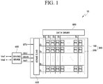
- FIG. 1 is a block diagram of a liquid crystal display 10 according to an exemplary embodiment of the present invention
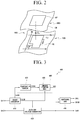
- FIG. 2 is an equivalent circuit diagram of a pixel in a liquid crystal display according to an exemplary embodiment of the present invention
- FIG. 3 is a block diagram of a driving device according to an exemplary embodiment of the present invention..
- the liquid crystal display 10 includes a liquid crystal panel 300, a gate driver 500, a data driver 600, and a driving device 400.
- the liquid crystal panel 300 includes a first plate having a plurality of gate lines G 1 - G n , a plurality of data lines D 1 - D m , a switching element (not shown), and a pixel electrode (not shown), and a second plate having a color filter (not shown) and a common electrode (CE) (not shown).
- the first plate 100 extends to be somewhat wider than the second plate 200.
- the gate lines G 1 - G n extend substantially in a row direction and parallel to each other, while the data lines D 1 - D m extend substantially in a column direction and parallel to each other.
- a color filter may be formed on a predetermined area of a common electrode (CE) provided on the second plate 200 so as to face a pixel electrode (PE) provided on the first plate 100.
- a pixel PX includes a switching element Q connected to signal lines G i and D j , a liquid crystal capacitor C lc and a storage capacitor C st that are connected to the pixel.
- the storage capacitor C st may be omitted if desired.
- the switching element Q is a TFT made of amorphous silicon (a-Si).
- the gate driver 500 of FIG. 1 is mounted on the extended region of the first plate 100.
- the gate driver 500 receives a clock signal CKV, a clock-bar signal CKVB, and a gate-off voltage Voff from the driving device 400, receives a vertical start signal STV indicating a vertical scanning start from a timing controller (not shown), and provides gate driving signals to the plurality of gate lines G 1 - G n .
- the data driver 600 is connected to the plurality of data lines D 1 -D n and provides data signals to the plurality of data lines D 1 -D n .
- the driving device 400 receives a first input voltage Vin1 and a second input voltage Vin2 from an external circuit (not shown) and provides the clock signal CKV, the clock-bar signal CKVB, and the gate-off voltage Voff to the gate driver 500.
- the clock signal CKV, the clock-bar signal CKVB, and the gate-off voltage Voff are signals for controlling on/off states of the plurality of gate lines G 1 - G n .
- the driving device 400 may be configured to provide only the clock signal CKV to the gate driver 500.
- the gate driver 500 converts the clock signal CKV into a clock bar signal CKVB for driving the plurality of gate lines G 1 - G n .
- the driving device 400 includes a boost converter 410, a gate-on voltage generator 440, a gate-off voltage generator 450, and a switching unit 460, as shown in FIG. 3 .
- the boost converter 410 receives and boosts the first input voltage Vin1 and generates a driving voltage AVDD and a pulse signal PULSE.
- the boost converter 410 may be a DC-DC converter or another kind of converter. The boost converter 410 will later be described with reference to FIG. 7 .
- the gate-on voltage generator 440 receives the driving voltage AVDD and the pulse signal PULSE from the boost converter 410 and generates a gate-on voltage Von.
- the level of the gate-on voltage Von is adjusted according to the ambient temperature.
- the gate-on voltage generator 440 includes a temperature sensor 420 and a charge pumping unit 430.
- the temperature sensor 420 produces a temperature-dependent variable voltage VARV, the level of which increases when the ambient temperature rises and vice versa.
- the charge pumping unit 430 receives the temperature-dependent variable voltage AVDD and the pulse signal PULSE, level-shifts the variable voltage VARV by the amplitude of the pulse signal PULSE, and generates the gate-on voltage Von. More specifically, when the ambient temperature decreases, the gate-on voltage generator 440 generates a gate-on voltage Von having an increased voltage level. On the contrary, when the ambient temperature increases, the gate-on voltage generator 440 generates a gate-on voltage Von having a decreased voltage level.
- the temperature sensor 420 and the charge pumping unit 430 will be described below in more detail with reference to FIGS. 4 and 5 , respectively.
- the gate-off voltage generator 450 receives the second input voltage Vin2 and the pulse signal PULSE from the boost converter 410 and generates a gate-off voltage Voff.
- the gate-off voltage Voff is maintained at a fixed value regardless of the ambient temperature.
- the gate-off voltage generator 450 will later be described in more detail with reference to FIG. 5 .
- the switching unit 460 generates a clock signal CKV and a clock bar signal CKVB swinging between the gate-on voltage Von and the gate-off voltage Voff. That is to say, a high level of the clock signal CKV corresponds to the voltage level of the gate-on voltage Von and a low level of the clock signal CKV corresponds to the voltage level of the gate-off voltage Voff.
- the clock signal CKV has a phase different from that of the clock bar signal CKVB.
- the clock signal CKV and the clock bar signal CKVB have phases opposite to each other.
- the switching unit 460 receives control signals from a timing controller (not shown) and performs a switching operation between the two output signals CKV and CKVB.
- the driving device 400 when the ambient temperature decreases, the driving device 400 outputs a clock signal CKV having an increased amplitude and a clock bar signal CKVB corresponding thereto of a different phase.
- the driving device 400 when the ambient temperature increases, the driving device 400 outputs a clock signal CKV having a decreased amplitude and a clock bar signal CKVB corresponding thereto having a different phase.
- the amplitudes of the clock signal CKV and the clock bar signal CKVB are adjusted according to a variation of the voltage level of Von depending on a change in the ambient temperature.
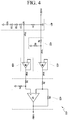
- FIG. 4 is a circuit diagram illustrating a temperature sensor (420) shown in FIG. 3 .
- the temperature sensor 420 includes a comparison voltage generator 421 shifting the voltage level of the driving voltage AVDD according to the ambient temperature and generating a comparison voltage Vcpr, a reference voltage generator 422 dividing the driving voltage AVDD and generating a reference voltage Vref, and an amplifier 423 amplifying a difference between the comparison voltage Vcpr and the reference voltage Vref.
- the comparison voltage generator 421 includes one or more diodes D1, D2, and D3 each having a variable threshold voltage.
- the threshold voltage of diodes D1, D2, and D3 is substantially inversely proportional to a change in the ambient temperature.
- the comparison voltage generator 421 includes a fixed resistor R1 that is connected between a first node N1 and a second node N2 and one or more diodes D1, D2, and D3 that are connected between the second node N2 and a third node N3.
- the driving voltage AVDD which is a positive voltage, is applied to the first node N1, and the comparison voltage Vcpr is output via the second node N2.
- the comparison voltage Vcpr also varies according to the ambient temperature. For example, assuming that the driving voltage AVDD is approximately 12 V and the threshold voltage of each of the diodes D1, D2, and D3 is approximately 0.57 V at room temperature, if the ambient temperature falls, the level of the comparison voltage Vcpr rises to approximately 2 V, which is due to an increase of a threshold voltage of the level of the comparison voltage Vcpr being approximately 1.7 V (3 X 0.57 V) at room temperature.
- the reference voltage generator 422 may be a voltage divider. That is to say, the reference voltage generator 422 generates the reference voltage Vref derived from the driving voltage AVDD divided by a plurality of resistors R2 and R3 connected in series. The level of the reference voltage Vref is maintained at a fixed value regardless of a change of the ambient temperature, because the resistance of the resistors does not change with temperature and the driving voltage AVDD is fixed.
- the reference voltage Vref is not restricted to a voltage obtained by dividing the driving voltage AVDD, and may thus be any arbitrary voltage.
- the amplifier 423 amplifies a difference between the comparison voltage Vcpr and the reference voltage Vref and outputs the temperature-dependent variable voltage VARV.
- the amplifier 423 which is a differential amplifier, includes two pairs of resistors R4 and R5 determining voltage gains and an operational amplifier OP.
- the amplifier 423 is not restricted to a differential amplifier.
- the temperature sensor 421 may also include a buffer 426, shown in FIG. 10 , that provides the amplifier 423 with the comparison voltage Vcpr as it is. If the reference voltage Vref is obtained by dividing the driving voltage AVDD, the temperature sensor 421 may also include a buffer (not shown) that provides the amplifier 423 with the reference voltage Vref as it is.
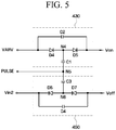
- FIG. 5 is a circuit diagram illustrating the charge pumping unit 430 and the gate-off voltage generator 450 shown in FIG. 3 .
- the charge pumping unit 430 includes fourth and fifth diodes D4 and D5 and first and second capacitors C1 and C2.
- the temperature-dependent variable voltage VARV is supplied to the anode terminal of the fourth diode D4, the cathode terminal of which is connected to a fourth node N4.
- the first capacitor C1 is connected between the fourth node N4 and a fifth node N5 to which the pulse signal PULSE is applied.
- the anode terminal of the fifth diode D5 is connected to the fourth node N4, and a gate-on voltage Von is output at the cathode terminal of the fifth diode D5.
- the second capacitor C2 is connected between the anode terminal of the fourth diode D4 and the cathode terminal of the fifth diode D5.
- the charge pumping unit 430 includes two diodes and two capacitors by way of example, the invention is not limited to the illustrated example and the charge pumping unit 430 may be configured by a combination of three or more diodes and three or more capacitors.
- the first node N1 outputs a pulse of a high voltage level increased by the voltage level of the pulse signal PULSE.
- the fifth diode D5 and the second capacitor C2 clamp the voltage of the fourth node N4 to then output the gate-on voltage Von.
- the gate-on voltage Von is a DC voltage shifted from the temperature-dependent variable voltage VARV by approximately the amplitude of the pulse signal PULSE.
- the gate-on voltage Von also varies in inverse proportion to temperature.
- the gate-off voltage generator 450 includes sixth and seventh diodes D6 and D7 and third and fourth capacitors C3 and C4.
- the second input voltage Vin2 is applied to the cathode terminal of the sixth diode D6, the anode terminal of which is connected to a sixth node N6.
- the third capacitor C3 is connected between the sixth node N6 and the fifth node N5 to which the pulse signal PULSE is applied.
- the cathode terminal of the seventh diode D7 is connected to the sixth node N6 and a gate-off voltage Voff is output to the anode terminal of the seventh diode D7.
- the fourth capacitor C4 is connected between the cathode terminal of the sixth diode D6 and the anode terminal of the seventh diode D7.
- the gate-off voltage generator 450 includes two diodes and two capacitors by way of example, the invention is not limited to the illustrated example and the gate-off voltage generator 450 may be configured by a combination of three or more diodes and three or more capacitors.
- the gate-off voltage generator 450 In the operation of the gate-off voltage generator 450, when the pulse signal PULSE is applied to the third capacitor C3, the sixth node N6 outputs a pulse of a low voltage level decreased by the voltage level of the pulse signal PULSE.
- the sixth diode D6 and the fourth capacitor C4 clamp the voltage of the sixth node N6 to then output a gate-off voltage Voff.
- the gate-off voltage Von is a DC voltage shifted from the second input voltage Vin2 by approximately the amplitude of the pulse signal PULSE.
- the second input voltage Vin2 may be a ground voltage.
- the gate-off voltage Voff may be a negative voltage and may also be not influenced by temperature.
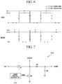
- a clock signal CKV and a clock bar signal CKVB that are obtained using the gate-on voltage Von and the gate-off voltage Voff are illustrated in FIG. 6 . That is, the clock signal CKV and the clock bar signal CKVB both swing between a gate-on voltage Von_H and the gate-off voltage Voff at high temperatures, whereas the clock signal CKV and the clock bar signal CKVB both swing between a gate-on voltage Von_L, which is higher than the Von_H, and the gate-off voltage Voff at low temperatures.
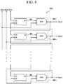
- FIG. 7 is circuit diagram illustrating the boost converter 410 used in the driving device 400 shown in FIG. 3 .
- the boost converter 410 includes an inductor L to which the first input voltage Vin1 is applied, an eighth diode D8, the anode terminal of which is connected to the inductor L and the cathode terminal of which is connected to the output terminal of the driving voltage AVDD, a sixth capacitor C6 connected between the cathode of the eighth diode D8 and a ground terminal, a switching element SW which is connected between the anode of the eighth diode D8 and a ground terminal, and a pulse width modulation (PWM) signal generator 415 which is connected to the gate of the switching element SW.
- PWM pulse width modulation
- the switching element SW is turned on.
- An end of the inductor L is connected to a ground terminal through the switching element SW, and the current I L flowing through the inductor L, which is proportional to the first input voltage Vin1 applied to opposite ends of the inductor L, increases slowly according to characteristics of the current and voltage of the inductor L.
- the switching element SW may be turned off,the current IL may flow through the inductor L via the eighth diode D8 and the sixth capacitor C6 may be charged according to characteristics of the current and voltage of the sixth capacitor C6. Accordingly, the first input voltage Vin1 is boosted to a predetermined voltage level to then be output as the driving voltage AVDD.
- the pulse signal PULSE swings between the driving voltage AVDD and a ground voltage. That is, the driving voltage AVDD and the amplitude of the pulse signal PULSE may be not influenced by temperature.
- the driving voltage AVDD may be provided to a gray voltage generator (not shown).
- the gray voltage generator may comprise a plurality of resistors each connected between each of nodes to which the driving voltage AVDD is applied and the ground terminal, to generate gray voltages by dividing the voltage level of the driving voltage AVDD.
- the internal circuit of the gray voltage generator is not limited to the stated example and various modifications and changes may be made.
- FIG. 8 is a block diagram illustrating the gate driver 500 shown in FIG. 1
- FIG. 9 is a circuit diagram illustrating a first stage shown in FIG. 8 .
- the gate driver 500 includes a plurality of stages SRC 1 , ... , SRC n that are cascade-connected to each other. More specifically, first through nth stages SRC 1 , ... , SRC n each includes an SR latch (SR 1 - SR n ) and an AND gate. In addition, the plurality of stages SRC 1 , ... , SRC n are connected to the gate lines G 1 - G n shown in FIG. 1 , respectively.
- the respective SR latches SR 1 - SR n are set, that is, activated, by gate driving signals Gout 1 - Gout n of a high level, which are supplied from the previous stage, and are reset, that is, deactivated, by gate driving signals Gout 1 - Gout n of a high level, which are fed back from the next or subsequent stage.
- the respective AND gate of each of the stages SRC 1 , ... , SRC n is set and the clock signal CKV or clock bar signal CKVB of a high level is supplied to the AND gate, the gate driving signals Gout 1 - Gout n are generated.
- the clock signal CKV and the clock bar signal CKVB can have phases opposite to each other.
- the gate driver 500 sequentially outputs the clock signal CKV or the clock bar signal CKVB of a high level to the gate lines G 1 - G n .
- each of the respective stages SRC 1 , ... , SRC n includes a plurality of transistors T1-T4 and a fifth capacitor C5.
- transistors T1-T4 transistors T1-T4
- C5 fifth capacitor
- a vertical start signal STV of a high level is fed to a seventh node N7 and supplied to the fifth capacitor C5 via the first transistor T1, which is a diode-connected transistor, the fifth capacitor C5 is charged with a voltage.
- the second transistor T2 is turned on.
- the clock signal CKV of a high level is supplied to the second transistor T2
- the clock signal CKV is output as the gate driving signal Gout 1 .
- the output gate driving signal Gout 1 which is the clock signal CKV of a high level, is a gate-on voltage Von.
- the third transistor T3 is turned on to discharge the voltage charged in the fifth capacitor C5 and the fourth transistor T4 is also turned on to pull the output gate driving signal Gout 1 of a high level down to the voltage level of the gate-off voltage Voff. Accordingly, the output gate driving signal Gout 1 falls to the gate-off voltage Voff.
- first through fourth transistors T1-T4 are NMOS TFTs by way of example, the invention is not limited to the illustrated example and the first through fourth transistors T1-T4 may be PMOS TFTs made of amorphous silicon (a-Si).
- a-Si amorphous silicon
- the current driving capacity of the switching element Q of FIG. 2 of a pixel and the second transistor T2 made of a-Si is reduced at a temperature lower than room temperature, resulting in a deterioration of a display quality. Nevertheless, since the driving device 400 of FIG. 1 provides the clock signal CKL having an increased amplitude at a low temperature, the display quality can be enhanced and not be deteriorated.
- the gate lines G 1 - G n shown in FIG. 1 have parasitic capacitance of several hundreds pF. If the current driving capacity of the second transistor T2 is decreased at a low temperature, the amount of charges supplied to charge parasitic capacitors of the gate lines G 1 - G n is reduced for a predetermined time. As a result, the gate-on voltage Von for driving the switching element Q of FIG. 2 within a pixel is reduced. In such a case, the display quality may deteriorate. Meanwhile, when the ambient temperature is low, the gate-on voltage generator 440 generates a gate-on voltage of a high level and a clock signal CKV based on the gate-on voltage of a high level is supplied to the gate driver 500.
- FIG. 10 is a circuit diagram of a temperature sensor 470 included in a driving device according to an exemplary embodiment of the present invention.
- Like reference numerals refer to like elements throughout the specification and drawings, and thus, detailed descriptions thereof will be skipped.
- a negative voltage is applied to a third node N3 of a comparison voltage generator 421.
- the negative voltage may be obtained by dividing a gate-off voltage Voff.
- the temperature sensor 470 may include a voltage divider 471 which divides a negative gate-off voltage Voff and provides a voltage obtained by the division to the third node N3.
- the range of variation of a comparison voltage Vcpr varies.
- the comparison voltage Vcpr may be higher than 0 V or may be a negative voltage.
- the voltage of the third node N3 may be varied according to the resistances of resistors R6 and R7 of the voltage divider 471.
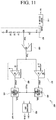
- FIG. 11 is a circuit diagram of a driving device 400' according to a comparative example of the present invention
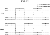
- FIG. 12 is a graph for explaining the output of the driving device 400' shown in FIG. 11 .
- Like reference numerals refer to like elements throughout the specification and drawings, and thus, detailed descriptions thereof will be skipped.
- a gate-off voltage Voff varies according to temperature.
- the amplitudes of a clock signal CKV and a clock bar signal CKVB increase.
- the driving device 400' includes a gate-on voltage generator, a gate-off voltage generator, and a switching unit.
- the gate-on voltage generator includes a first temperature sensor 421, 426, and 427 and a first charge pumping unit 430.
- the gate-off voltage generator includes a second temperature sensors 421, 426, and 428 and a second charge-pumping unit 450. That is, the first temperature sensor 421, 426, and 427 and the second temperature sensor 421, 426, and 428 may share the comparison voltage generator 421 and the buffer 426.
- a ground voltage may be applied to a third node N3 of the comparison voltage generator 421, but the present invention is not restricted to this. That is, a negative voltage obtained by dividing a gate-off voltage Voff may be applied to the third node N3 of the comparison voltage generator 421.
- the first temperature sensor 421, 426, and 427 receives a comparison voltage Vcpr and outputs a first temperature-dependent variable voltage VARV1. As the temperature increases, the first temperature-dependent variable voltage VARV1 decreases. On the other hand, as the temperature decreases, the first temperature-dependent variable voltage VARV1 increases.
- the first temperature sensor 421, 426, and 427 may include a non-inverting amplifier 427.
- the non-inverting amplifier 427 receives the comparison voltage Vcpr that varies in inverse proportion to temperature and generates the first temperature-dependent variable voltage VARV1 by amplifying the comparison voltage Vcpr.
- the second temperature sensor 421, 426, and 428 receives the comparison voltage Vcpr and outputs a second temperature-dependent variable voltage VARV2. As the temperature increases, the second temperature-dependent variable voltage VARV2 increases. On the other hand, as temperature decreases, the second temperature-dependent variable voltage VARV2 decreases.
- the second temperature sensor 421, 426, and 428 may include an inverting amplifier 428.
- the inverting amplifier 428 is provided with the comparison voltage Vcpr that varies in proportion to temperature and generates the second temperature-dependent variable voltage VARV2 by amplifying the comparison voltage Vcpr while inverting the phase of the comparison voltage Vcpr.
- the first and second charge-pumping units 430 and 450 receive the first and second temperature-dependent variable voltages VARV1 and VARV2, respectively, and output the gate-on voltage Von and the gate-off voltage Voff, respectively, which vary according to temperature.
- the switching unit 460 of FIG. 3 generates the clock signal CKV and the clock bar signal CKVB using the gate-on voltage Von and the gate-off voltage Voff.
- the clock signal CKV and the clock bar signal CKVB are illustrated in FIG. 12 . Referring to FIG. 12 , the clock signal CKV and the clock bar signal CKVB swing between a gate-on voltage Von_H and a gate-off voltage Voff_H at high temperatures, whereas the clock signal CKV and the clock bar signal CKVB swing between a gate-on voltage Von_L, which is higher than the gate-on voltage Von_H, and a gate-off voltage Voff_L, which is lower than the gate-off voltage Voff_H, at low temperatures.
- the driving device 400' can provide the clock signal CKV and the clock bar signal CKVB whose amplitudes increase according to temperature. Therefore, a display apparatus including the driving device 400' can enhance the quality of display of images even at low temperatures.
Claims (4)
- Affichage à cristaux liquides (10) à matrice active au silicium amorphe, comprenant un générateur de tension de grille (440) qui comprend :un capteur de température (420) comprenant un amplificateur opérationnel (OP), le capteur de température (420 ; 470) étant configuré pour recevoir une tension d'excitation (AVDD) et produire une tension variable dépendante de la température (VARV) dont le niveau varie selon la température ambiante ; etune unité de pompage de charge (430) adaptée pour décaler la tension variable dépendante de la température (VARV) de l'amplitude d'un signal d'impulsion (PULSE) qui lui est transmis et pour générer une tension de grille (Von),dans lequel le capteur de température (420) comprend une ou plusieurs diodes (D1 ; D2 ; D3), chacune des une ou plusieurs diodes (D1 ; D2 ; D3) ayant une tension de seuil variable inhérente caractéristique de la diode en question qui varie avec la température ambiante, et les une ou plusieurs diodes étant adaptées pour produire une tension de comparaison variable (Vcpr) en fonction de la variation de la tension de seuil variable inhérente caractéristique de l'une ou des plusieurs diodes (D1 ; D2 ; D3), la tension de comparaison variable (Vcpr) étant amenée à une entrée de l'amplificateur opérationnel (OP) ;dans lequel le signal d'impulsion (PULSE) transmis à l'unité de pompage de charge (430) est un signal modulé en amplitude ;dans lequel le niveau de tension de la tension variable dépendante de la température (VARV) augmente quand la température ambiante baisse et le niveau de tension de la tension variable dépendante de la température (VARV) baisse quand la température ambiante augmente ; etdans lequel la tension de grille (Von) augmente quand la température ambiante baisse ;caractérisé en ce qu'un convertisseur survolteur (410) est connecté au générateur de tension de grille (440), le convertisseur survolteur (410) étant configuré pour recevoir et élever une première tension d'entrée (Vin1) et émettre en sortie ladite tension d'excitation (AVDD) et ledit signal d'impulsion (PULSE), la température ambiante n'ayant pas d'influence sur la tension d'excitation (AVDD) et l'amplitude du signal d'impulsion (PULSE) ;dans lequel le capteur de température (420) comprend un générateur de tension de référence (422) adapté pour diviser la tension d'excitation (AVDD) et générer une tension de référence (Vref) un générateur de tension de comparaison (421) comprenant lesdites une ou plusieurs diodes (D1 ; D2 ; D3),
etun amplificateur (423), incluant l'amplificateur opérationnel (OP), qui amplifie une différence entre la tension de comparaison variable (Vcpr) et la tension de référence (Vref) pour produire la tension variable dépendante de la température (VARV),
etdans lequel le convertisseur survolteur (410) inclut une bobine d'induction (L) dont une première extrémité est adaptée pour recevoir la première tension d'entrée (Vin1), une huitième diode (D8), la borne d'anode de la huitième diode (D8) étant connectée à la deuxième extrémité de la bobine d'induction (L) et la borne de cathode de la huitième diode (D8) à la borne de sortie de la tension d'excitation (AVDD), un élément de commutation (SW) connecté à l'anode de la huitième diode (D8) et à une tension de masse, une capacité (C6) connectée entre la borne de cathode de la huitième diode (D8) et la tension de masse et un générateur de signal (415) de modulation d'amplitude (PWM) connecté à la grille de l'élément de commutation,le signal sur la borne d'anode de la huitième diode (D8) étant émis en sortie comme signal d'impulsion (PULSE) vers l'unité de pompage de charge. - Affichage à cristaux liquides (10) selon la revendication 1, dans lequel le générateur de tension de comparaison (421) inclut en outre une résistance fixe (R1) connectée entre une premier noeud (N1) et un deuxième noeud (N2) et les diodes (D1 ; D2 ; D3) connectées en série entre le deuxième noeud (N2) et un troisième noeud (N3), et dans lequel une tension positive est appliquée au premier noeud (N1), la tension de comparaison (Vcpr) est émise en sortie via le deuxième noeud (N2) et une tension de masse est appliquée au troisième noeud (N3).
- Affichage à cristaux liquides (10) selon la revendication 1, dans lequel le générateur de tension de comparaison (421) comprend en outre une résistance fixe (R1) connectée entre un premier noeud (N1) et un deuxième noeud (N2) et les diodes (D1 ; D2 ; D3) connectées en série entre le deuxième noeud (N2) et un troisième noeud (N3), une tension positive étant appliquée au premier noeud (N1), la tension de comparaison (Vcpr) étant émise en sortie via le deuxième noeud (N2) et une tension négative étant appliquée au troisième noeud (N3).
- Affichage à cristaux liquides (10) selon la revendication 2, dans lequel le capteur de température (420) comprend en outre un tampon qui fournit la tension de comparaison (Vcpr) à l'amplificateur (423) sans altération.
Applications Claiming Priority (3)
| Application Number | Priority Date | Filing Date | Title |
|---|---|---|---|
| KR20060066012 | 2006-07-13 | ||
| KR1020070038497A KR101385229B1 (ko) | 2006-07-13 | 2007-04-19 | 게이트 온 전압 발생 회로, 구동 장치 및 이를 포함하는표시 장치 |
| EP07012429A EP1879174A3 (fr) | 2006-07-13 | 2007-06-26 | Générateur de tension pour la commande de grille, dispositif de commande et appareil d'affichage équipé de celui-ci |
Related Parent Applications (1)
| Application Number | Title | Priority Date | Filing Date |
|---|---|---|---|
| EP07012429A Division EP1879174A3 (fr) | 2006-07-13 | 2007-06-26 | Générateur de tension pour la commande de grille, dispositif de commande et appareil d'affichage équipé de celui-ci |
Publications (2)
| Publication Number | Publication Date |
|---|---|
| EP3032528A1 EP3032528A1 (fr) | 2016-06-15 |
| EP3032528B1 true EP3032528B1 (fr) | 2018-01-17 |
Family
ID=38566049
Family Applications (2)
| Application Number | Title | Priority Date | Filing Date |
|---|---|---|---|
| EP16152615.7A Active EP3032528B1 (fr) | 2006-07-13 | 2007-06-26 | Générateur de tension, dispositif de commande et appareil d'affichage équipé de celui-ci |
| EP07012429A Ceased EP1879174A3 (fr) | 2006-07-13 | 2007-06-26 | Générateur de tension pour la commande de grille, dispositif de commande et appareil d'affichage équipé de celui-ci |
Family Applications After (1)
| Application Number | Title | Priority Date | Filing Date |
|---|---|---|---|
| EP07012429A Ceased EP1879174A3 (fr) | 2006-07-13 | 2007-06-26 | Générateur de tension pour la commande de grille, dispositif de commande et appareil d'affichage équipé de celui-ci |
Country Status (5)
| Country | Link |
|---|---|
| US (2) | US8692751B2 (fr) |
| EP (2) | EP3032528B1 (fr) |
| JP (1) | JP5366375B2 (fr) |
| KR (1) | KR101385229B1 (fr) |
| CN (1) | CN101105923B (fr) |
Cited By (1)
| Publication number | Priority date | Publication date | Assignee | Title |
|---|---|---|---|---|
| CN107424577A (zh) * | 2017-08-15 | 2017-12-01 | 京东方科技集团股份有限公司 | 一种显示驱动电路、显示装置及其驱动方法 |
Families Citing this family (39)
| Publication number | Priority date | Publication date | Assignee | Title |
|---|---|---|---|---|
| KR101385229B1 (ko) * | 2006-07-13 | 2014-04-14 | 삼성디스플레이 주식회사 | 게이트 온 전압 발생 회로, 구동 장치 및 이를 포함하는표시 장치 |
| KR101294321B1 (ko) * | 2006-11-28 | 2013-08-08 | 삼성디스플레이 주식회사 | 액정 표시 장치 |
| KR100909251B1 (ko) * | 2007-01-31 | 2009-07-23 | 주식회사 하이닉스반도체 | 아날로그-디지털 변환기 및 이를 포함하는 온도정보출력장치 |
| KR100865852B1 (ko) * | 2007-08-08 | 2008-10-29 | 주식회사 하이닉스반도체 | 레귤레이터 및 고전압 발생기 |
| KR101472076B1 (ko) * | 2008-08-12 | 2014-12-15 | 삼성디스플레이 주식회사 | 액정 표시 장치 |
| KR101545697B1 (ko) * | 2008-08-29 | 2015-08-21 | 삼성디스플레이 주식회사 | 액정 표시 장치 |
| JP2010224594A (ja) * | 2009-03-19 | 2010-10-07 | Oki Semiconductor Co Ltd | 電圧発生回路 |
| JP4924700B2 (ja) * | 2009-11-20 | 2012-04-25 | 株式会社デンソー | 物理量検出装置 |
| KR101712070B1 (ko) * | 2010-05-06 | 2017-03-06 | 삼성디스플레이 주식회사 | 전압 발생회로 및 이를 구비한 표시장치 |
| TWI433088B (zh) | 2010-10-27 | 2014-04-01 | Chunghwa Picture Tubes Ltd | 顯示裝置及驅動方法 |
| TWI406502B (zh) * | 2010-12-14 | 2013-08-21 | Au Optronics Corp | 具有自動線性溫度調整功能之閘極驅動電路 |
| CN102034453B (zh) * | 2010-12-30 | 2013-02-13 | 福建华映显示科技有限公司 | 液晶面板的工作电压切换系统及其切换方法 |
| KR101745418B1 (ko) * | 2010-12-30 | 2017-06-12 | 엘지디스플레이 주식회사 | 전원 공급부 및 이를 포함하는 액정표시장치 |
| TWI549430B (zh) * | 2011-03-30 | 2016-09-11 | 友達光電股份有限公司 | 具有溫度補償之穩壓電路模組 |
| KR101202745B1 (ko) * | 2011-04-21 | 2012-11-19 | 주식회사 실리콘웍스 | 터치감지회로 |
| KR102016554B1 (ko) * | 2011-11-24 | 2019-09-02 | 삼성디스플레이 주식회사 | 액정 표시 장치 |
| CN103218962B (zh) * | 2012-01-20 | 2015-10-28 | 群康科技(深圳)有限公司 | 移位寄存器 |
| US8710900B2 (en) * | 2012-03-22 | 2014-04-29 | Fairchild Semiconductor Corporation | Methods and apparatus for voltage selection for a MOSFET switch device |
| CN102663980B (zh) * | 2012-04-13 | 2014-10-29 | 北京京东方光电科技有限公司 | 一种栅极驱动电路的控制电路及其工作方法、液晶显示器 |
| TWI478142B (zh) * | 2012-11-01 | 2015-03-21 | Au Optronics Corp | 顯示裝置與其驅動模組、電壓控制電路和方法 |
| FR3010224B1 (fr) * | 2013-08-30 | 2016-11-11 | Thales Sa | Ecran a matrice active a regulation de tensions d'alimentation en fonction de la temperature |
| KR102126799B1 (ko) * | 2013-10-25 | 2020-06-26 | 삼성디스플레이 주식회사 | Dcdc 컨버터, 이를 구비한 표시 장치 및 이를 이용한 표시 패널의 구동 방법 |
| US9690306B2 (en) * | 2013-11-01 | 2017-06-27 | Blackberry Limited | Display interface temperature compensation |
| KR102229005B1 (ko) * | 2014-10-10 | 2021-03-18 | 엘지디스플레이 주식회사 | 게이트 구동회로와 이를 이용한 표시장치 |
| KR102250309B1 (ko) * | 2014-10-13 | 2021-05-12 | 삼성디스플레이 주식회사 | 표시 장치 및 표시 장치의 구동 방법 |
| JP2016183932A (ja) * | 2015-03-26 | 2016-10-20 | 株式会社東芝 | 温度センサ回路 |
| CN105118451B (zh) * | 2015-08-19 | 2018-02-23 | 深圳市华星光电技术有限公司 | 驱动电路以及液晶显示装置 |
| KR102422744B1 (ko) * | 2015-10-01 | 2022-07-19 | 삼성디스플레이 주식회사 | 표시장치 및 그의 구동방법 |
| KR102582656B1 (ko) * | 2016-08-31 | 2023-09-25 | 삼성디스플레이 주식회사 | 표시 장치의 온도 보상 전원 회로 |
| CN109949758B (zh) * | 2017-12-21 | 2022-01-04 | 咸阳彩虹光电科技有限公司 | 基于栅极驱动电路的扫描信号补偿方法及装置 |
| TWI658304B (zh) * | 2018-01-15 | 2019-05-01 | 友達光電股份有限公司 | 顯示裝置 |
| CN107993607B (zh) * | 2018-01-23 | 2020-07-10 | 京东方科技集团股份有限公司 | 栅极驱动单元及其驱动方法、栅极驱动电路和显示装置 |
| CN108766381B (zh) * | 2018-06-01 | 2020-08-11 | 京东方科技集团股份有限公司 | 一种移位寄存器电路、阵列基板和显示装置 |
| CN108550352B (zh) * | 2018-07-26 | 2021-05-18 | 京东方科技集团股份有限公司 | 栅极电压控制电路、栅极驱动电路及显示装置 |
| CN108831406B (zh) | 2018-09-20 | 2021-10-22 | 京东方科技集团股份有限公司 | 电压提供电路、栅极驱动信号提供模组、方法和显示面板 |
| KR102635405B1 (ko) * | 2019-02-26 | 2024-02-14 | 삼성디스플레이 주식회사 | 표시 장치 |
| CN110910818B (zh) * | 2019-12-06 | 2021-09-21 | 业成科技(成都)有限公司 | 逆向电流检测电路及具有逆向电流检测电路的显示装置 |
| CN111369942B (zh) * | 2020-03-26 | 2022-01-14 | 维沃移动通信有限公司 | 驱动电压调整方法和电子设备 |
| TWI738417B (zh) * | 2020-07-10 | 2021-09-01 | 友達光電股份有限公司 | 顯示裝置以及驅動方法 |
Family Cites Families (17)
| Publication number | Priority date | Publication date | Assignee | Title |
|---|---|---|---|---|
| SE404108B (sv) | 1977-02-10 | 1978-09-18 | Philips Svenska Ab | Anordning for overvakning av temperaturen hos en elektrisk komponent |
| FR2539932A1 (fr) | 1983-01-21 | 1984-07-27 | Thomson Csf | Dispositif de compensation des derives du gain en temperature, d'un amplificateur de signaux electriques hyperfrequences |
| JP3230010B2 (ja) * | 1992-02-28 | 2001-11-19 | キヤノン株式会社 | 液晶カラー表示装置 |
| JP3068465B2 (ja) * | 1996-07-12 | 2000-07-24 | 日本電気株式会社 | 液晶表示装置 |
| KR100223154B1 (en) * | 1996-12-18 | 1999-10-15 | Lg Electronics Inc | Temperature compensation circuit for liquid crystal display device |
| JPH1114961A (ja) | 1997-04-28 | 1999-01-22 | Toshiba Microelectron Corp | 液晶駆動用回路 |
| US6333728B1 (en) * | 1998-09-03 | 2001-12-25 | International Business Machines Corporation | Method and apparatus for real-time on-off contrast ratio optimization in liquid crystal displays |
| JP2001169273A (ja) | 1999-12-06 | 2001-06-22 | Sharp Corp | カラーテレビドアホン装置 |
| KR100683519B1 (ko) * | 1999-12-23 | 2007-02-15 | 엘지.필립스 엘시디 주식회사 | 액정 패널의 충전 특성 보상회로 및 충전 특성 보상방법 |
| US7262752B2 (en) * | 2001-01-16 | 2007-08-28 | Visteon Global Technologies, Inc. | Series led backlight control circuit |
| JP3990167B2 (ja) * | 2002-03-04 | 2007-10-10 | Nec液晶テクノロジー株式会社 | 液晶表示装置の駆動方法およびその駆動方法を用いた液晶表示装置 |
| KR100992135B1 (ko) * | 2003-11-10 | 2010-11-04 | 삼성전자주식회사 | 액정 표시 장치의 구동 장치 |
| GB0402046D0 (en) * | 2004-01-29 | 2004-03-03 | Koninkl Philips Electronics Nv | Active matrix display device |
| KR101056374B1 (ko) | 2004-02-20 | 2011-08-11 | 삼성전자주식회사 | 펄스 보상기, 이를 갖는 영상표시장치 및 영상표시장치의구동방법 |
| CN100458906C (zh) * | 2004-02-20 | 2009-02-04 | 三星电子株式会社 | 脉冲补偿器、显示装置及驱动该显示装置的方法 |
| KR101021202B1 (ko) * | 2004-04-16 | 2011-03-11 | 엘지디스플레이 주식회사 | 저온 온도보상 구동회로를 구비한 에프에스씨 모드액정표시장치 및 그 구동방법 |
| KR101385229B1 (ko) * | 2006-07-13 | 2014-04-14 | 삼성디스플레이 주식회사 | 게이트 온 전압 발생 회로, 구동 장치 및 이를 포함하는표시 장치 |
-
2007
- 2007-04-19 KR KR1020070038497A patent/KR101385229B1/ko active IP Right Grant
- 2007-06-14 US US11/763,123 patent/US8692751B2/en active Active
- 2007-06-26 EP EP16152615.7A patent/EP3032528B1/fr active Active
- 2007-06-26 EP EP07012429A patent/EP1879174A3/fr not_active Ceased
- 2007-07-05 JP JP2007177122A patent/JP5366375B2/ja active Active
- 2007-07-12 CN CN200710136271.XA patent/CN101105923B/zh active Active
-
2014
- 2014-02-10 US US14/176,872 patent/US9035861B2/en active Active
Non-Patent Citations (1)
| Title |
|---|
| None * |
Cited By (1)
| Publication number | Priority date | Publication date | Assignee | Title |
|---|---|---|---|---|
| CN107424577A (zh) * | 2017-08-15 | 2017-12-01 | 京东方科技集团股份有限公司 | 一种显示驱动电路、显示装置及其驱动方法 |
Also Published As
| Publication number | Publication date |
|---|---|
| US9035861B2 (en) | 2015-05-19 |
| EP1879174A3 (fr) | 2009-07-01 |
| US20140176624A1 (en) | 2014-06-26 |
| US20080054987A1 (en) | 2008-03-06 |
| US8692751B2 (en) | 2014-04-08 |
| CN101105923A (zh) | 2008-01-16 |
| JP5366375B2 (ja) | 2013-12-11 |
| JP2008020911A (ja) | 2008-01-31 |
| KR101385229B1 (ko) | 2014-04-14 |
| KR20080007087A (ko) | 2008-01-17 |
| EP3032528A1 (fr) | 2016-06-15 |
| EP1879174A2 (fr) | 2008-01-16 |
| CN101105923B (zh) | 2014-08-06 |
Similar Documents
| Publication | Publication Date | Title |
|---|---|---|
| EP3032528B1 (fr) | Générateur de tension, dispositif de commande et appareil d'affichage équipé de celui-ci | |
| US20090102779A1 (en) | Gate-off volatage generating circuit, driving device and liquid crystal dispaly including the same | |
| US11580926B2 (en) | Display panel having a gate driver integrated therein | |
| JP5388400B2 (ja) | パルス補償器、これを有する画像表示装置、及び画像表示装置の駆動方法 | |
| JP5086692B2 (ja) | 液晶表示装置 | |
| KR101545697B1 (ko) | 액정 표시 장치 | |
| US8730146B2 (en) | Drive voltage generating circuit and liquid crystal display including the same | |
| US8847869B2 (en) | Liquid crystal display device and method for driving the same | |
| US20170032758A1 (en) | Gamma reference voltage generator and display device having the same | |
| KR101056374B1 (ko) | 펄스 보상기, 이를 갖는 영상표시장치 및 영상표시장치의구동방법 | |
| US20180294728A1 (en) | Gate line drive circuit and display device having the same | |
| US20240144893A1 (en) | Display panel | |
| KR20090005861A (ko) | 액정 표시 장치 | |
| KR20080044444A (ko) | 전압 발생 장치 및 이를 포함하는 액정 표시 장치 |
Legal Events
| Date | Code | Title | Description |
|---|---|---|---|
| PUAI | Public reference made under article 153(3) epc to a published international application that has entered the european phase |
Free format text: ORIGINAL CODE: 0009012 |
|
| AC | Divisional application: reference to earlier application |
Ref document number: 1879174 Country of ref document: EP Kind code of ref document: P |
|
| AK | Designated contracting states |
Kind code of ref document: A1 Designated state(s): AT BE BG CH CY CZ DE DK EE ES FI FR GB GR HU IE IS IT LI LT LU LV MC MT NL PL PT RO SE SI SK TR |
|
| AX | Request for extension of the european patent |
Extension state: AL BA HR MK RS |
|
| 17P | Request for examination filed |
Effective date: 20161213 |
|
| RBV | Designated contracting states (corrected) |
Designated state(s): AT BE BG CH CY CZ DE DK EE ES FI FR GB GR HU IE IS IT LI LT LU LV MC MT NL PL PT RO SE SI SK TR |
|
| GRAP | Despatch of communication of intention to grant a patent |
Free format text: ORIGINAL CODE: EPIDOSNIGR1 |
|
| RIC1 | Information provided on ipc code assigned before grant |
Ipc: G09G 3/36 20060101AFI20170711BHEP Ipc: H03K 5/13 20140101ALN20170711BHEP Ipc: H02M 3/07 20060101ALN20170711BHEP |
|
| RIC1 | Information provided on ipc code assigned before grant |
Ipc: H03K 5/13 20140101ALN20170720BHEP Ipc: G09G 3/36 20060101AFI20170720BHEP Ipc: H02M 3/07 20060101ALN20170720BHEP |
|
| INTG | Intention to grant announced |
Effective date: 20170809 |
|
| RAP1 | Party data changed (applicant data changed or rights of an application transferred) |
Owner name: SAMSUNG DISPLAY CO., LTD. |
|
| RIN1 | Information on inventor provided before grant (corrected) |
Inventor name: CHOI, YUN-SEOK Inventor name: LEE, YONG-SOON |
|
| GRAS | Grant fee paid |
Free format text: ORIGINAL CODE: EPIDOSNIGR3 |
|
| GRAA | (expected) grant |
Free format text: ORIGINAL CODE: 0009210 |
|
| AC | Divisional application: reference to earlier application |
Ref document number: 1879174 Country of ref document: EP Kind code of ref document: P |
|
| AK | Designated contracting states |
Kind code of ref document: B1 Designated state(s): AT BE BG CH CY CZ DE DK EE ES FI FR GB GR HU IE IS IT LI LT LU LV MC MT NL PL PT RO SE SI SK TR |
|
| REG | Reference to a national code |
Ref country code: GB Ref legal event code: FG4D |
|
| REG | Reference to a national code |
Ref country code: CH Ref legal event code: EP |
|
| REG | Reference to a national code |
Ref country code: IE Ref legal event code: FG4D |
|
| REG | Reference to a national code |
Ref country code: AT Ref legal event code: REF Ref document number: 964917 Country of ref document: AT Kind code of ref document: T Effective date: 20180215 |
|
| REG | Reference to a national code |
Ref country code: DE Ref legal event code: R096 Ref document number: 602007053789 Country of ref document: DE |
|
| REG | Reference to a national code |
Ref country code: NL Ref legal event code: MP Effective date: 20180117 |
|
| REG | Reference to a national code |
Ref country code: LT Ref legal event code: MG4D |
|
| REG | Reference to a national code |
Ref country code: AT Ref legal event code: MK05 Ref document number: 964917 Country of ref document: AT Kind code of ref document: T Effective date: 20180117 |
|
| PG25 | Lapsed in a contracting state [announced via postgrant information from national office to epo] |
Ref country code: NL Free format text: LAPSE BECAUSE OF FAILURE TO SUBMIT A TRANSLATION OF THE DESCRIPTION OR TO PAY THE FEE WITHIN THE PRESCRIBED TIME-LIMIT Effective date: 20180117 |
|
| PG25 | Lapsed in a contracting state [announced via postgrant information from national office to epo] |
Ref country code: ES Free format text: LAPSE BECAUSE OF FAILURE TO SUBMIT A TRANSLATION OF THE DESCRIPTION OR TO PAY THE FEE WITHIN THE PRESCRIBED TIME-LIMIT Effective date: 20180117 Ref country code: FI Free format text: LAPSE BECAUSE OF FAILURE TO SUBMIT A TRANSLATION OF THE DESCRIPTION OR TO PAY THE FEE WITHIN THE PRESCRIBED TIME-LIMIT Effective date: 20180117 Ref country code: LT Free format text: LAPSE BECAUSE OF FAILURE TO SUBMIT A TRANSLATION OF THE DESCRIPTION OR TO PAY THE FEE WITHIN THE PRESCRIBED TIME-LIMIT Effective date: 20180117 Ref country code: CY Free format text: LAPSE BECAUSE OF FAILURE TO SUBMIT A TRANSLATION OF THE DESCRIPTION OR TO PAY THE FEE WITHIN THE PRESCRIBED TIME-LIMIT Effective date: 20180117 |
|
| REG | Reference to a national code |
Ref country code: FR Ref legal event code: PLFP Year of fee payment: 12 |
|
| PG25 | Lapsed in a contracting state [announced via postgrant information from national office to epo] |
Ref country code: IS Free format text: LAPSE BECAUSE OF FAILURE TO SUBMIT A TRANSLATION OF THE DESCRIPTION OR TO PAY THE FEE WITHIN THE PRESCRIBED TIME-LIMIT Effective date: 20180517 Ref country code: LV Free format text: LAPSE BECAUSE OF FAILURE TO SUBMIT A TRANSLATION OF THE DESCRIPTION OR TO PAY THE FEE WITHIN THE PRESCRIBED TIME-LIMIT Effective date: 20180117 Ref country code: SE Free format text: LAPSE BECAUSE OF FAILURE TO SUBMIT A TRANSLATION OF THE DESCRIPTION OR TO PAY THE FEE WITHIN THE PRESCRIBED TIME-LIMIT Effective date: 20180117 Ref country code: GR Free format text: LAPSE BECAUSE OF FAILURE TO SUBMIT A TRANSLATION OF THE DESCRIPTION OR TO PAY THE FEE WITHIN THE PRESCRIBED TIME-LIMIT Effective date: 20180418 Ref country code: BG Free format text: LAPSE BECAUSE OF FAILURE TO SUBMIT A TRANSLATION OF THE DESCRIPTION OR TO PAY THE FEE WITHIN THE PRESCRIBED TIME-LIMIT Effective date: 20180417 Ref country code: PL Free format text: LAPSE BECAUSE OF FAILURE TO SUBMIT A TRANSLATION OF THE DESCRIPTION OR TO PAY THE FEE WITHIN THE PRESCRIBED TIME-LIMIT Effective date: 20180117 Ref country code: AT Free format text: LAPSE BECAUSE OF FAILURE TO SUBMIT A TRANSLATION OF THE DESCRIPTION OR TO PAY THE FEE WITHIN THE PRESCRIBED TIME-LIMIT Effective date: 20180117 |
|
| REG | Reference to a national code |
Ref country code: DE Ref legal event code: R097 Ref document number: 602007053789 Country of ref document: DE |
|
| PG25 | Lapsed in a contracting state [announced via postgrant information from national office to epo] |
Ref country code: RO Free format text: LAPSE BECAUSE OF FAILURE TO SUBMIT A TRANSLATION OF THE DESCRIPTION OR TO PAY THE FEE WITHIN THE PRESCRIBED TIME-LIMIT Effective date: 20180117 Ref country code: EE Free format text: LAPSE BECAUSE OF FAILURE TO SUBMIT A TRANSLATION OF THE DESCRIPTION OR TO PAY THE FEE WITHIN THE PRESCRIBED TIME-LIMIT Effective date: 20180117 Ref country code: IT Free format text: LAPSE BECAUSE OF FAILURE TO SUBMIT A TRANSLATION OF THE DESCRIPTION OR TO PAY THE FEE WITHIN THE PRESCRIBED TIME-LIMIT Effective date: 20180117 |
|
| PLBE | No opposition filed within time limit |
Free format text: ORIGINAL CODE: 0009261 |
|
| STAA | Information on the status of an ep patent application or granted ep patent |
Free format text: STATUS: NO OPPOSITION FILED WITHIN TIME LIMIT |
|
| PG25 | Lapsed in a contracting state [announced via postgrant information from national office to epo] |
Ref country code: CZ Free format text: LAPSE BECAUSE OF FAILURE TO SUBMIT A TRANSLATION OF THE DESCRIPTION OR TO PAY THE FEE WITHIN THE PRESCRIBED TIME-LIMIT Effective date: 20180117 Ref country code: SK Free format text: LAPSE BECAUSE OF FAILURE TO SUBMIT A TRANSLATION OF THE DESCRIPTION OR TO PAY THE FEE WITHIN THE PRESCRIBED TIME-LIMIT Effective date: 20180117 Ref country code: DK Free format text: LAPSE BECAUSE OF FAILURE TO SUBMIT A TRANSLATION OF THE DESCRIPTION OR TO PAY THE FEE WITHIN THE PRESCRIBED TIME-LIMIT Effective date: 20180117 |
|
| 26N | No opposition filed |
Effective date: 20181018 |
|
| REG | Reference to a national code |
Ref country code: CH Ref legal event code: PL |
|
| PG25 | Lapsed in a contracting state [announced via postgrant information from national office to epo] |
Ref country code: SI Free format text: LAPSE BECAUSE OF FAILURE TO SUBMIT A TRANSLATION OF THE DESCRIPTION OR TO PAY THE FEE WITHIN THE PRESCRIBED TIME-LIMIT Effective date: 20180117 |
|
| REG | Reference to a national code |
Ref country code: BE Ref legal event code: MM Effective date: 20180630 |
|
| REG | Reference to a national code |
Ref country code: IE Ref legal event code: MM4A |
|
| PG25 | Lapsed in a contracting state [announced via postgrant information from national office to epo] |
Ref country code: LU Free format text: LAPSE BECAUSE OF NON-PAYMENT OF DUE FEES Effective date: 20180626 Ref country code: MC Free format text: LAPSE BECAUSE OF FAILURE TO SUBMIT A TRANSLATION OF THE DESCRIPTION OR TO PAY THE FEE WITHIN THE PRESCRIBED TIME-LIMIT Effective date: 20180117 |
|
| PG25 | Lapsed in a contracting state [announced via postgrant information from national office to epo] |
Ref country code: LI Free format text: LAPSE BECAUSE OF NON-PAYMENT OF DUE FEES Effective date: 20180630 Ref country code: IE Free format text: LAPSE BECAUSE OF NON-PAYMENT OF DUE FEES Effective date: 20180626 Ref country code: CH Free format text: LAPSE BECAUSE OF NON-PAYMENT OF DUE FEES Effective date: 20180630 |
|
| PG25 | Lapsed in a contracting state [announced via postgrant information from national office to epo] |
Ref country code: BE Free format text: LAPSE BECAUSE OF NON-PAYMENT OF DUE FEES Effective date: 20180630 |
|
| PG25 | Lapsed in a contracting state [announced via postgrant information from national office to epo] |
Ref country code: MT Free format text: LAPSE BECAUSE OF NON-PAYMENT OF DUE FEES Effective date: 20180626 |
|
| PG25 | Lapsed in a contracting state [announced via postgrant information from national office to epo] |
Ref country code: TR Free format text: LAPSE BECAUSE OF FAILURE TO SUBMIT A TRANSLATION OF THE DESCRIPTION OR TO PAY THE FEE WITHIN THE PRESCRIBED TIME-LIMIT Effective date: 20180117 |
|
| PG25 | Lapsed in a contracting state [announced via postgrant information from national office to epo] |
Ref country code: PT Free format text: LAPSE BECAUSE OF FAILURE TO SUBMIT A TRANSLATION OF THE DESCRIPTION OR TO PAY THE FEE WITHIN THE PRESCRIBED TIME-LIMIT Effective date: 20180117 |
|
| PG25 | Lapsed in a contracting state [announced via postgrant information from national office to epo] |
Ref country code: HU Free format text: LAPSE BECAUSE OF FAILURE TO SUBMIT A TRANSLATION OF THE DESCRIPTION OR TO PAY THE FEE WITHIN THE PRESCRIBED TIME-LIMIT; INVALID AB INITIO Effective date: 20070626 |
|
| P01 | Opt-out of the competence of the unified patent court (upc) registered |
Effective date: 20230515 |
|
| PGFP | Annual fee paid to national office [announced via postgrant information from national office to epo] |
Ref country code: FR Payment date: 20230522 Year of fee payment: 17 Ref country code: DE Payment date: 20230522 Year of fee payment: 17 |
|
| PGFP | Annual fee paid to national office [announced via postgrant information from national office to epo] |
Ref country code: GB Payment date: 20230523 Year of fee payment: 17 |