EP3028353B1 - Dispositif laser à polarisation réglable - Google Patents
Dispositif laser à polarisation réglable Download PDFInfo
- Publication number
- EP3028353B1 EP3028353B1 EP14744344.4A EP14744344A EP3028353B1 EP 3028353 B1 EP3028353 B1 EP 3028353B1 EP 14744344 A EP14744344 A EP 14744344A EP 3028353 B1 EP3028353 B1 EP 3028353B1
- Authority
- EP
- European Patent Office
- Prior art keywords
- laser light
- laser
- polarization
- sub
- array
- Prior art date
- Legal status (The legal status is an assumption and is not a legal conclusion. Google has not performed a legal analysis and makes no representation as to the accuracy of the status listed.)
- Active
Links
- 230000010287 polarization Effects 0.000 title claims description 175
- 238000003491 array Methods 0.000 claims description 28
- 230000003287 optical effect Effects 0.000 claims description 26
- 238000001514 detection method Methods 0.000 claims description 22
- 238000012545 processing Methods 0.000 claims description 22
- 230000001427 coherent effect Effects 0.000 claims description 14
- 238000000034 method Methods 0.000 claims description 13
- 230000008859 change Effects 0.000 description 8
- 238000013459 approach Methods 0.000 description 7
- 230000008901 benefit Effects 0.000 description 6
- 238000005259 measurement Methods 0.000 description 6
- 230000008878 coupling Effects 0.000 description 3
- 238000010168 coupling process Methods 0.000 description 3
- 238000005859 coupling reaction Methods 0.000 description 3
- 238000005530 etching Methods 0.000 description 3
- 230000001788 irregular Effects 0.000 description 3
- 230000003595 spectral effect Effects 0.000 description 3
- 230000001419 dependent effect Effects 0.000 description 2
- 238000004519 manufacturing process Methods 0.000 description 2
- 238000012986 modification Methods 0.000 description 2
- 230000004048 modification Effects 0.000 description 2
- 230000008569 process Effects 0.000 description 2
- 239000004065 semiconductor Substances 0.000 description 2
- 230000035945 sensitivity Effects 0.000 description 2
- 238000004458 analytical method Methods 0.000 description 1
- 238000006243 chemical reaction Methods 0.000 description 1
- 238000013016 damping Methods 0.000 description 1
- 230000005284 excitation Effects 0.000 description 1
- 230000002349 favourable effect Effects 0.000 description 1
- 238000002329 infrared spectrum Methods 0.000 description 1
- 239000002245 particle Substances 0.000 description 1
- 230000003252 repetitive effect Effects 0.000 description 1
- 238000004611 spectroscopical analysis Methods 0.000 description 1
- 238000012546 transfer Methods 0.000 description 1
- 230000001960 triggered effect Effects 0.000 description 1
- 238000001429 visible spectrum Methods 0.000 description 1
Images


Classifications
-
- H—ELECTRICITY
- H01—ELECTRIC ELEMENTS
- H01S—DEVICES USING THE PROCESS OF LIGHT AMPLIFICATION BY STIMULATED EMISSION OF RADIATION [LASER] TO AMPLIFY OR GENERATE LIGHT; DEVICES USING STIMULATED EMISSION OF ELECTROMAGNETIC RADIATION IN WAVE RANGES OTHER THAN OPTICAL
- H01S5/00—Semiconductor lasers
- H01S5/10—Construction or shape of the optical resonator, e.g. extended or external cavity, coupled cavities, bent-guide, varying width, thickness or composition of the active region
- H01S5/18—Surface-emitting [SE] lasers, e.g. having both horizontal and vertical cavities
- H01S5/183—Surface-emitting [SE] lasers, e.g. having both horizontal and vertical cavities having only vertical cavities, e.g. vertical cavity surface-emitting lasers [VCSEL]
- H01S5/18355—Surface-emitting [SE] lasers, e.g. having both horizontal and vertical cavities having only vertical cavities, e.g. vertical cavity surface-emitting lasers [VCSEL] having a defined polarisation
-
- G—PHYSICS
- G01—MEASURING; TESTING
- G01B—MEASURING LENGTH, THICKNESS OR SIMILAR LINEAR DIMENSIONS; MEASURING ANGLES; MEASURING AREAS; MEASURING IRREGULARITIES OF SURFACES OR CONTOURS
- G01B11/00—Measuring arrangements characterised by the use of optical techniques
- G01B11/24—Measuring arrangements characterised by the use of optical techniques for measuring contours or curvatures
- G01B11/25—Measuring arrangements characterised by the use of optical techniques for measuring contours or curvatures by projecting a pattern, e.g. one or more lines, moiré fringes on the object
-
- G—PHYSICS
- G01—MEASURING; TESTING
- G01J—MEASUREMENT OF INTENSITY, VELOCITY, SPECTRAL CONTENT, POLARISATION, PHASE OR PULSE CHARACTERISTICS OF INFRARED, VISIBLE OR ULTRAVIOLET LIGHT; COLORIMETRY; RADIATION PYROMETRY
- G01J4/00—Measuring polarisation of light
- G01J4/04—Polarimeters using electric detection means
-
- G—PHYSICS
- G06—COMPUTING; CALCULATING OR COUNTING
- G06T—IMAGE DATA PROCESSING OR GENERATION, IN GENERAL
- G06T7/00—Image analysis
- G06T7/50—Depth or shape recovery
- G06T7/55—Depth or shape recovery from multiple images
- G06T7/593—Depth or shape recovery from multiple images from stereo images
-
- H—ELECTRICITY
- H01—ELECTRIC ELEMENTS
- H01S—DEVICES USING THE PROCESS OF LIGHT AMPLIFICATION BY STIMULATED EMISSION OF RADIATION [LASER] TO AMPLIFY OR GENERATE LIGHT; DEVICES USING STIMULATED EMISSION OF ELECTROMAGNETIC RADIATION IN WAVE RANGES OTHER THAN OPTICAL
- H01S5/00—Semiconductor lasers
- H01S5/06—Arrangements for controlling the laser output parameters, e.g. by operating on the active medium
- H01S5/068—Stabilisation of laser output parameters
- H01S5/06821—Stabilising other output parameters than intensity or frequency, e.g. phase, polarisation or far-fields
-
- H—ELECTRICITY
- H01—ELECTRIC ELEMENTS
- H01S—DEVICES USING THE PROCESS OF LIGHT AMPLIFICATION BY STIMULATED EMISSION OF RADIATION [LASER] TO AMPLIFY OR GENERATE LIGHT; DEVICES USING STIMULATED EMISSION OF ELECTROMAGNETIC RADIATION IN WAVE RANGES OTHER THAN OPTICAL
- H01S5/00—Semiconductor lasers
- H01S5/10—Construction or shape of the optical resonator, e.g. extended or external cavity, coupled cavities, bent-guide, varying width, thickness or composition of the active region
- H01S5/18—Surface-emitting [SE] lasers, e.g. having both horizontal and vertical cavities
- H01S5/183—Surface-emitting [SE] lasers, e.g. having both horizontal and vertical cavities having only vertical cavities, e.g. vertical cavity surface-emitting lasers [VCSEL]
- H01S5/18386—Details of the emission surface for influencing the near- or far-field, e.g. a grating on the surface
-
- H—ELECTRICITY
- H01—ELECTRIC ELEMENTS
- H01S—DEVICES USING THE PROCESS OF LIGHT AMPLIFICATION BY STIMULATED EMISSION OF RADIATION [LASER] TO AMPLIFY OR GENERATE LIGHT; DEVICES USING STIMULATED EMISSION OF ELECTROMAGNETIC RADIATION IN WAVE RANGES OTHER THAN OPTICAL
- H01S5/00—Semiconductor lasers
- H01S5/40—Arrangement of two or more semiconductor lasers, not provided for in groups H01S5/02 - H01S5/30
- H01S5/42—Arrays of surface emitting lasers
- H01S5/423—Arrays of surface emitting lasers having a vertical cavity
-
- H—ELECTRICITY
- H04—ELECTRIC COMMUNICATION TECHNIQUE
- H04N—PICTORIAL COMMUNICATION, e.g. TELEVISION
- H04N13/00—Stereoscopic video systems; Multi-view video systems; Details thereof
- H04N13/20—Image signal generators
- H04N13/204—Image signal generators using stereoscopic image cameras
Definitions
- the invention relates to a laser device with adjustable polarization, a sensor device and an optical detection system comprising such a laser device.
- the invention further relates to a method of determining a three dimensional shape of an object.
- WO 01/05008 A1 discloses the control of polarization of the laser emission of a Vertical Cavity Surface Emitting Lasers (VCSELs). Furthermore, the fabrication of arrays of polarization controlled VCSELs of the same polarization by means of one dimensional grating structure over the entire array of VCSELs in a single processing step is described.
- VCSELs Vertical Cavity Surface Emitting Lasers
- the described arrays lack of flexibility such that the potential applications are limited.
- a laser device according to the present invention is defined by claim 1 and a method of determining the shape of an object using such a laser device is defined by claim 13.
- a laser device comprising an array of laser emitters and a control unit.
- the array comprises at least a first sub array of laser emitters and a second sub array of laser emitters, wherein the first sub array emits laser light of a first polarization and the second sub array emits laser light of a second polarization being different from the first polarization.
- the first sub array and/or the second sub array comprise subsets of the laser emitters.
- the control unit is adapted to control the first sub array and the second sub array such that the polarization of the laser light emitted by the array can be controlled.
- a subset of coherent laser emitters emit coherent laser light of a defined polarization whereby two or more subsets of the sub array emit incoherent laser light of the defined polarization. At least the laser light emitted by a first subset is not coherent to laser light emitted by a second subset.
- the control unit is further adapted to control subsets of the laser emitters of the first sub array and/or the second sub array independently such that the coherence of the emitted laser light can be controlled.
- the control unit is adapted to control the coherence of the emitted laser light by means of the at least first subset and the at least second subset.
- the laser emitters are preferably semiconductor lasers as Vertical Cavity Surface Emitting Laser (VCSEL) or side emitter.
- VCSEL may have the advantage that they can be produced on wafer scale such that arrays of VCSELs emitting laser light of different polarization can be produced by means of a surface grating on top of the light emitting surface on each VCSEL.
- the surface gratings of a multitude of VCSEL can be produced in one etching step.
- Side emitters may have the advantage that they are inherently polarized. No additional technical measures are thus needed in order to get laser emitters of a defined polarization.
- the first sub array and the second sub array may be integrated on one chip.
- the chip may comprise a first contiguous area of laser devices emitting laser light of the first polarization and a second contiguous area of laser devices emitting laser light of the second polarization.
- the chip may also comprise three, four or more contiguous areas comprising sub arrays of laser emitters emitting laser light of a third, fourth or more polarization. It may also be possible that two or more sub arrays provided on contiguous areas emit laser light of the same polarization. Such contiguous areas may be squares, rectangles, triangle or line or stripes of laser devices emitting laser light of the first and second polarization.
- the sub arrays may share the same area on the chip.
- Adjacent laser emitters may emit in this case laser light of different polarization.
- three, four or more laser emitters emitting laser light of different polarizations may be subsequently arranged in a line in a repetitive order or in two or more lines. The sequence of the laser emitters in the lines may be shifted or the order may even be changed.
- the pattern of laser emitters emitting laser light of different polarization may thus be regular or irregular.
- Arranging the laser emitters emitting laser light of different polarization next to each other may have the advantage that a pattern of laser dots of different polarization may be directly projected onto an object without additional optical elements.
- a simple arrangement of lenses may be sufficient to widen such a pattern of laser dots.
- the sub arrays of laser emitters emitting laser light of a defined polarization may alternatively be arranged on different chips. Different polarizations may in this case be enabled by turning the chips relative to each other by, for example, 45 °, 90°, 120° or other angles depending on the number of chips or sub arrays used within the array and the number of polarizations needed for the respective application.
- the control unit may control the sub arrays independently with respect to each other.
- the polarization of the laser light emitted by the laser device may thus continuously be changed from laser light of the first polarization (only the first sub array emits laser light) to laser light without polarization (both sub arrays emit laser light of the same intensity) to laser light of the second polarization (only the second sub array emits laser light).
- An additional polarizer under the right angle may be added, such that the polarization can be switched between left and right circularly polarized.
- a more sophisticated control may be enabled by coherent coupling of the laser devices of each sub array allowing even in the case of only two sub arrays a continuous change of the angle of polarization.
- the laser emitters of the sub arrays are arranged in subsets.
- the subsets are controlled independently by means of the controller. The latter may enable a simplified control of the laser device in comparison to the control of each laser emitter.
- the laser emitters of the subsets are coherently coupled such that the coherence of the laser light emitted by the sub arrays is controllable.
- a subset of coherent laser emitters emit in this case coherent laser light of a defined polarization whereby two or more subsets of the sub array emit incoherent laser light of the defined polarization if they are controlled by means of the controller to emit laser light at the same time.
- sub arrays of different polarization may enable to emit laser light of more than two polarizations by switching on the respective sub array by means of the controller of the laser device.
- the power provided to each sub array may be controllable in a continuous way. Furthermore it may be possible to power only a part of the laser emitters or even single laser of the sub array by means of the controller.
- the controller will be connected to an external power supply or an internal power supply e.g. battery.
- a sensor device may comprise the laser device described above and a detector.
- the detector may be adapted to detect the different polarizations of laser light emitted by the sub arrays after reflection of the emitted laser light by an object.
- the detector may comprise a camera chip like a Charge Coupled Device (CCD) or the like and a polarization filter.
- the polarization filter may be fixed or controllable by means of a control module.
- a controllable polarization filter may enable to adjust the polarization of the laser light received by the camera chip automatically. It may also be possible to use a detector without polarization filter.
- the control module may in this case be adapted to submit the laser light of different polarizations in a way that no polarization filter is needed.
- a control signal may, for example, be submitted by means of the laser device and received by means of the detector such that the polarization of the laser light is identified by means of the control signal.
- the control signal may be used in subsequent processing by means of, for example, the control module of the sensor or an analyzing unit the sensor device is coupled with in order to identify the respective polarization of the laser light.
- An object may be illuminated with laser light of changing polarizations and local variations of the intensity of the reflected laser light in combination with the information about the polarization of the emitted laser light may enable an analysis of the surface properties of the object.
- a polarizing beam splitter and two camera chips are used.
- the polarizing beam splitter may be arranged to transfer laser light of a first polarization to a first camera chip and laser light of a second polarization to a second camera chip such that the intensities of the laser light of the two polarizations can be independently detected.
- the laser device may in this case only provide laser light of two different preferably orthogonal polarizations.
- the polarizing beam splitter may be a beam splitter in combination with two polarization filter with orthogonal polarization.
- An optical detection system may comprise the laser device described above.
- the optical detection system further comprises a receiver and a processing unit.
- the processing unit may be any kind of processor, microprocessor or computer including one or more memory devices.
- the laser device may be adapted to emit a pattern of laser light comprising at least a first sub pattern of laser light with a first polarization and a second sub pattern of laser light with a second polarization.
- the receiver may be adapted to receive the first and the second sub pattern emitted by the laser device reflected by an object, and the processing unit may be adapted to determine the shape of the object by means of the reflected first and second sub pattern.
- the receiver may, for example, comprise a camera chip and a polarization filter of a defined polarization.
- the processing unit may communicate with the control unit of the laser device.
- the laser device may emit a pattern of dots with different polarization and exchange the respective information with the processing unit such that the processing unit is informed about the respective pattern.
- Each pattern may comprise a unique identifier emitted by means of the laser device, for example, prior to the emission of the pattern such that the processing unit is informed when the respective pattern is received by means of the receiver.
- the control unit may further be adapted to change the pattern.
- the processing unit may thus be able to determine the shape of the object by comparing the information about the emitted pattern and the received pattern based on a multitude of different patterns.
- the detector may comprise in an alternative approach a detector with a controllable polarization filter.
- the laser device may emit in this case a constant pattern and the control module may change the setting of the controllable polarization filter such that laser light of different polarizations can pass the controllable polarization at different times.
- Information about the emitted pattern, the distortion of the received pattern and the intensity of the dots of the pattern in relation to the setting of the controllable polarization filter may be used by means of the processing unit in order to determine the shape of the object.
- the optical detection system may further comprise a camera for recording a picture of the object.
- the processing unit may be adapted to determine a three-dimensional picture of the object based on the determined shape of the object and the picture of the object.
- the information provided by means of a conventional camera may be combined with the determined shape of the object. It may thus be possible to provide a realistic three dimensional picture of the object.
- the use of a polarization filter in front of the receiver reduces the intensity of the ambient light by 50 % such that the contrast of the pattern may be improved.
- the pattern is preferably emitted in a different wavelength as the picture (e.g. infrared spectrum in comparison to visible spectrum recorded by the camera) such that the pattern of laser light may not disturb recording of the picture by means of the camera.
- a method of determining the shape of an object comprises the steps of:
- the information provided by means of the first and the second sub pattern may improve the determination of the shape of the object by providing additional information via the different polarization of the laser light in the sub pattern.
- the method may comprise the additional step of providing the pattern of laser light, wherein the pattern changes in time and providing information about the change to a processing unit such that the shape of the object is determined based on the information.
- the method comprises the step of changing the setting of a controllable polarization filter such that laser light of different polarization can be filtered in order to provide additional information about the object.
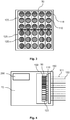
- Fig. 1 shows a principal sketch of a first laser device 10.
- the laser device 10 comprises a control unit 200 and an array 50 of laser emitters 100.
- the laser emitters 100 are arranged in a first sub array of laser emitters 110 emitting laser light of a first polarization 111 and a second sub array of laser emitters 120 emitting laser light of a second polarization 122.
- the laser emitters 100 are, for example, Vertical Cavity Surface Emitting Lasers (VCSELs) with a grating provided on the laser light emitting surface of the VCSELs in order to set the polarization of the laser light emitted by the respective VCSEL.
- VCSELs Vertical Cavity Surface Emitting Lasers
- the control unit 200 is adapted to control the first and the second sub array of laser emitters 110, 120 independently.
- the first sub array of laser emitters 110 may, for example, be powered at a time t 1 when the second sub array of laser emitters 120 is not powered.
- the second sub array of laser emitters 120 is powered when the first sub array of laser emitters 110 is not powered.
- the control unit may also be adapted to power each of the first and the second sub arrays of laser emitters 110, 120 at each intermediate power level between zero power and full power. Furthermore, both sub arrays may be powered at the same time.
- the polarization state of the emitted laser light 111, 122 may thus be controlled in a continuous way.
- Fig. 2 shows a chip 60 on which the VCSELs 100 of the laser array 50 are arranged and attached to.
- the first and the second sub arrays of laser emitters 110, 120 are arranged in a checker board pattern and emit laser light of a first polarization 111 and laser light of a second polarization 122 being perpendicular or orthogonal to the first polarization.
- a checker board pattern as well as, for example, a hexagonal pattern or the like may have the advantage that no optical element may be needed in order to overlap the emission of the respective sub array.
- the polarization of the array emission can only be varied between polarized in the two orthogonal polarization directions and unpolarized emission with varying degree of polarization.
- An additional polarizer may be added under the right angle, so that the polarization can be switched between left and right circularly polarized. Additional measures to coherently couple the emission of all elements in the array 50 that emit the same polarization will allow changing the angle of the polarization continuously. Such measures for coherent coupling of VCSELs are for example described in J. Baier, U. Weichmann; Extended cavity semiconductor laser device with increased intensity, US 2010/0265975 A1 .
- VCSELs Vertical Cavity Surface Emitting Lasers
- more than two sub arrays may be arranged on the chip 60 if adjacent laser emitters 100 do emit laser light of different polarization.
- the polarization of laser emitters 100 may, for example, change stepwise for 120° in case of three sub arrays, wherein in the case of four sub arrays the polarization may change for 45°. In this way a multitude of different polarization states are possible. It may even be possible to have an irregular pattern of laser emitters 100 with different polarization.
- the latter may be easily enabled by means of VCSELs produced in wafer process such that only one mask is needed in order to define the polarization of the laser light emitted by each VCSEL by providing different surface gratings in one etching step.
- the polarization of the sub arrays may be stored in a memory device of the control unit 200 or it may be determined by means of a suitable detector receiving only laser light of a defined polarization state in a calibration procedure.
- the laser light emitted by the laser emitters 100 of the array 50 may be manipulated by means of suitable optical elements.
- a lens may, for example be used to widen the beam of emitted laser light.
- Mirrors may be used to change the direction of the complete beam or parts of the beam.
- Fig. 3 shows an alternative arrangement of laser emitters 100 in an array 50.
- a first chip 115 comprising 5 subsets of laser emitters 105 emitting laser light of a first polarization and a second chip 125 comprising 5 subsets of laser emitters 105 emitting laser light of a second polarization is depicted.
- Each subset of laser emitters 105 can be driven independently.
- the number of laser emitters 100 per subset and the number of subsets per polarization may determine the degree of control about the polarization of the laser light emitted by means of the array 50 in case the subsets can only be switched on and off. The latter may limit the complexity of the control unit 200 needed to control the array 50.
- a continuous control may be enabled if the power supplied to each subset of laser emitters 105 can be controlled in a continuous way.
- the laser emitters 100 are in this case edge emitting laser diodes emitting polarized laser light. 15 edge emitting lasers are arranged on the first chip 115 and further 15 on the second chip 125 and aligned with respect to the polarization of the laser light emitted by means of the edge emitting laser. The polarization of the laser light emitted by means of the laser emitters 100 arranged on the second chip is twisted by 90°by twisting the edge emitting lasers by 90° in comparison to the edge emitting lasers attached to the first chip 115.
- the laser emitters may be arranged in the same way with respect to polarization of the emitted on each sub array of laser emitters 110, 120.
- the latter means that the polarization of the emitted laser light with respect to the longer side of the first or second chip 115, 125 may be the same.
- the polarization of the emitted laser light may be twisted by means of twisting the first and the second chip 115, 125 relative to each other.
- the shape of the chips may be used in this case to arrange the sub arrays. Chips with laser emitters 100 with the shape of an equilateral triangle may be used to provide laser light of three different polarizations in an easy way by simply turning the chips on a suitable circuit board.
- the shape of the chips may determine the number of possible polarizations of the emitted laser light. Alternatively, it may also be possible to provide quadratic or circular chips and arrange these chips on a circuit board or base chip in order to provide as much different polarizations of the emitted laser light as needed for the respective purpose.
- the size and number of laser emitters 100 per array 50, sub array 110, 120 or subset 105 may be used to control the coherence of the emitted laser light. Only coherently coupled laser emitters 100 emit coherent laser light. The coherence may thus be controlled by means of the control unit 200 by means of using subsets 105 or sub arrays which are not coherently coupled. It may even be favorable to combine single laser emitters 100 in an array 50 which are not coherently coupled.
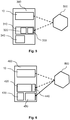
- Fig. 4 shows a laser device 10 comprising an array 50 depicted in Fig. 3 .
- the control unit 200 controls each subset of laser emitters 105 by simply switching the subset on or off.
- the laser device 10 further comprises an optical device 150 in order to superimpose the laser light emitted by the first and the second sub array of laser emitters 110, 120.
- the optical device 150 may comprise two diffractive elements in order to provide, for example, a superimposed checker board pattern of laser spots with alternating polarization of the laser light.
- arrangements of mirrors, semitransparent mirrors and lenses may be used to provide similar patterns.
- Projection lenses may be used in addition or alternatively to provide a pattern of lines with different polarization of the laser light of adjacent lines.
- the lines may be projected in a vertical or a horizontal direction with respect to a reference surface.
- the projection lenses and/or additional optical elements may even by switchable such that, for example, the pattern of lines can be switched between vertical and horizontal.
- more sophisticated patterns and switching states may be enabled by means of suitable optical devices 150. Switching of the optical device 150 may be controlled by means of the control unit 200. Alternatively, an additional control device may be used to control switching of the optical device 150.
- Optical devices 150 discussed in the framework of the embodiment shown in Fig. 4 may also be used to enable switching the pattern of laser beams emitted by a laser device 10 shown in Fig. 1 .
- Fig. 5 shows a principal sketch of a sensor device 300 in accordance with an embodiment of the present invention.
- the sensor device 300 comprises a laser device 10 as, for example, discussed above.
- the laser device 10 emits laser light of a first polarization and a second polarization perpendicular to the first polarization.
- the laser light is reflected by an object 500 and received by means of a camera chip 320 after passing an adjustable polarization filter 330.
- the camera chip 320 and the polarization filter 330 are part of a detector 310.
- a control module 340 controls the detector 320 and comprises a memory device (not shown) for storing the measurement results received by means of the detector 310.
- the polarization of the laser light passing the polarization filter may be, for example, adjusted by means of the control module 340.
- the control module 340 may in an alternative approach be adapted to control the laser device 10. This may happen via the control unit 200 of the laser device 10.
- the control unit 200 may in this case be triggered by means of the control module 340.
- the control module 340 may control the laser device 10 such that the laser device 10 emits laser light of the first polarization at time t 1 and laser light of the second polarization at a subsequent time t 2 .
- the control module 340 may know in this case when laser light of a defined polarization is emitted and the time when the respective laser light is received by means of the detector may be calculated if the distance to the object 500 is known.
- the distance to the object 500 may be fixed in certain applications of the sensor device 300 but in other applications a distance measurement may be needed.
- Such distance measurements may, for example, be performed by means of time of flight measurements or laser self-mixing using a suitable distance sensor (not shown) which may be controlled by means of the control module 340.
- a polarization filter 330 may be superfluous in such cases.
- the control module 340 determines the polarization of the laser light based on the time of emission of the laser light with a defined polarization and the time of receiving the respective laser light based on the known distance. It may be even possible to waive the distance sensor in case of an unknown distance.
- the control module 340 may, for example, emit a unique sequence of laser pulses be specific for each polarization of the laser light emitted by the laser device 10.
- the detector 310 determines the respective polarization of the received laser light by means of the sequence of laser pulses such neither a polarization filter 330 nor any knowledge about the distance to the object 50 may be necessary. This approach of identifying a measurement beam of laser light may be used in each case where the emitted laser light is characterized in certain way as, for example, a defined polarization as discussed above or a defined coherence.
- the control module 340 and the control unit 200 may even be one device controlling both the laser device 10 and the detector 310.
- the sensor device 300 may further comprise optical elements and/or mechanical elements which are adapted to direct or focus the laser light to the object 500.
- the laser device 10 and/ or the detector 310 may, for example, be rotatable around one or more axes.
- the sensor device 300 may be used in biosensor applications like, for example, handheld diagnostics.
- This biosensor gives a simple way to switch between bright- and dark-field detection.
- the reflected light from one polarization leads to a signal (bright field), while the other polarization will not lead to any signal (dark field).
- Particles on the surface will scatter the laser light emitted by the laser device 10 and change the polarization of the laser light, so they are seen as dark spots in bright-field detection and as signal in dark-field detection. In that way both ways of detection can be used and a high sensitivity reached.
- the sensor device 300 can be found in the fields of spectroscopy and sensing. The ability of simple switching between bright and dark field detection can be used to increase the sensitivity of these applications.
- Another field of application for such sensor devices 300 is photochemistry, where different chemical reactions can be steered by changing the polarization of the excitation.
- Fig. 6 shows a principal sketch of an optical detection system 400.
- the optical detection system 400 comprises a laser device 10 emitting a pattern of laser light with different polarizations.
- the pattern may be a line pattern with alternating lines of laser light of different polarization as depicted in Fig. 7.
- Fig. 7 shows a cylinder illuminated by means of the laser device 10 with a line pattern.
- a first sub pattern 510 comprises laser light of a first polarization parallel to the surface the object 500 is placed on and a second sub pattern 520 of laser light of a second polarization orthogonal to the surface the object 500 is placed on.
- a dot pattern of laser spots having different polarizations with respect to adjacent laser spots may be emitted by means of the laser device 10.
- the pattern may be regular or irregular.
- the optical detection system 400 further comprises a receiver 420 as, for example, a camera chip for receiving laser light reflected by the object 500 and a controllable polarizer 440.
- the controllable polarizer 440 is switched by means of a processing unit 430 between the different polarizations of laser light emitted by the laser device 10.
- the processing unit 430 may be used to control the laser device 10, the receiver 420 and the controllable polarizer 440 in the same or similar way as described with respect to the sensor device discussed above.
- the processing unit 400 may be further adapted to determine the three dimensional shape of the object 500 based on the distortion of the pattern caused by the shape of the object 500.
- the polarization of the laser light is used to improve the uniqueness of the emitted pattern. This may enable an improved detection of three dimensional objects in comparison to known approaches using structured light for three dimensional detection by means of triangulation because the different polarization add additional information to the pattern. Especially changing patterns of, for example, vertical and parallel lines of different polarization in a subsequent order may improve the detection by providing information about the shape of the object 500 in the horizontal and vertical direction.
- Using polarized light may increase the contrast because light of a polarization which is blocked by the adjustable polarization filter 440 does not disturb the measurement.
- known but highly unique patterns of a multitude of different polarizations as discussed above may be projected on a three dimensional object.
- the different spots of a defined polarization may be detected by means of the receiver 420 after passing the adjustable polarization filter 440. If more than two polarizations are used the intensity of the received laser light may be used as additional information because only a defined part of the reflected laser light with a polarization not parallel to the adjustable polarization filter 440 passes the adjustable polarization filter 440 and is received by means of the receiver 420. It may also be possible to subsequently send sub patterns of laser light with two or more polarization by controlling the laser emitters 100, the subsets of laser emitters 105 or the sub arrays accordingly.
- the processing unit 430 may process the patterns received by the receiver 420 such that even the shape of a moving object 500 may be determined. A three dimensional film of the moving object 500 may thus be provided.
- the optical detection device shown in Fig. 5 further comprises an optional camera 450 for receiving a conventional picture of the object 500.
- the laser device 10 may comprise laser emitters 100 like VCSEL emitting laser light in the infrared spectral range.
- the laser pattern thus does not disturb recording of the conventional picture by means of the camera 450.
- ambient light reflected by the object 500 and passing the controllable polarization filter 440 is damped by 50 %, whereby the laser light in line with the controllable polarization filter 440 passes the filter without damping.
- the contrast of the received pattern in relation to ambient light may thus be improved.
- a spectral filter may be added to the receiver 420 such that ambient light outside of the spectral range of the laser emitters 100 does not contribute to signal received by means of the receiver 420.
- VCSEL as laser emitters 100 may have the additional advantage that the shape of the aperture of adjacent VCSELs may be different by using an appropriate etching mask in the production process.
- the aperture of the VCSELs influences the form of the projected laser dots such that this additional measure may be used to add further information to the pattern of laser light.
- Fig. 8 shows a principal sketch of a method of determining the shape of an object 500.
- a pattern of laser light comprising at least a first sub pattern of laser light with a first polarization 510 and a second sub pattern of laser light with a second polarization 520 is provided.
- laser light of the pattern of laser light reflected by an object 500 is received.
- the shape of the object 500 is determined based on the received laser light.
Claims (13)
- Dispositif laser (10) comprenant un réseau (50) d'émetteurs laser (100) et une unité de commande (200), le réseau (50) comprenant au moins un premier sous-réseau (110) d'émetteurs laser et un second sous-réseau (120) d'émetteurs laser, dans lequel le premier sous-réseau (110) émet de la lumière laser d'une première polarisation (111) et le second sous-réseau (120) émet de la lumière laser d'une seconde polarisation (122) différente de la première polarisation, dans lequel le premier sous-réseau (110) et/ou le second sous-réseau (120) comprennent des sous-ensembles (105) des émetteurs laser (100) et l'unité de commande (200) est conçue pour commander le premier sous-réseau (110) et le second sous-réseau (120) de telle sorte que la polarisation de la lumière laser émise par le réseau (50) puisse être modifiée, caractérisé en ce que l'unité de commande (200) est conçue en outre pour commander les sous-ensembles (105) des émetteurs laser (100) du premier sous-réseau (110) et/ou du second sous-réseau (120) séparément, en ce qu'un sous-ensemble d'émetteurs laser cohérents émettent de la lumière laser cohérente d'une polarisation définie moyennant quoi deux sous-ensembles ou plusieurs du sous-réseau émettent de la lumière laser incohérente de la polarisation définie, en ce qu'au moins la lumière laser émise par un premier sous-ensemble (105) n'est pas cohérente avec la lumière laser émise par un second sous-ensemble (105), et en ce que l'unité de commande (200) est conçue en outre pour commander la cohérence de la lumière laser émise par le dispositif laser au moyen de l'au moins un premier sous-ensemble (105) et de l'au moins un second sous-ensemble (105).
- Dispositif laser (10) selon la revendication 1, dans lequel les émetteurs laser (100) sont des émetteurs laser à cavité verticale émettant par la surface et comprenant un réseau de diffraction permettant l'émission de lumière laser polarisée.
- Dispositif laser (10) selon la revendication 2, dans lequel le premier sous-réseau (110) et le second sous-réseau (120) sont intégrés sur une seule puce (60).
- Dispositif laser (10) selon la revendication 1 ou 2, dans lequel le premier sous-réseau (110) est agencé sur une première puce (115) et le second sous-réseau (120) est agencé sur une seconde puce (125).
- Dispositif laser (10) selon la revendication 3, dans lequel l'émetteur laser (100) du premier sous-réseau (110) et l'émetteur laser du second sous-réseau (120) sont agencés selon un motif en damier ou hexagonal.
- Dispositif laser (10) selon la revendication 1 ou 2, dans lequel le réseau (50) comprend une pluralité de sous-réseaux (110, 120), chaque sous-réseau (110, 120) émettant de la lumière laser de polarisation différente et dans lequel l'unité de commande (200) est conçue pour commander chaque sous-réseau (110, 120) de façon indépendante.
- Dispositif capteur (300) comprenant un dispositif laser (10) selon l'une quelconque des revendications 1 à 6 et un détecteur (310) conçu pour détecter différentes polarisations d'une lumière laser émise par les sous-réseaux (110, 120) et réfléchie par un objet (500).
- Dispositif capteur (300) selon la revendication 7, dans lequel le détecteur (310) comprend une puce caméra (320) et un filtre de polarisation (330).
- Dispositif capteur (300) selon la revendication 8, dans lequel le filtre de polarisation (330) est un filtre de polarisation réglable, et dans lequel le détecteur comprend un module de commande (340) conçu pour commander le filtre de polarisation (330) de sorte qu'une polarisation de la lumière laser reçue par la caméra (320) puisse être réglée automatiquement.
- Système de détection optique (400) comprenant un dispositif laser (10) selon l'une quelconque des revendications 1 à 6, un récepteur (420) et une unité de traitement (430), le dispositif laser (10) étant conçu pour émettre un motif de lumière laser comprenant au moins un premier sous-motif de lumière laser doté d'une première polarisation (510) et un second sous-motif de lumière laser doté d'une seconde polarisation (520), le récepteur (420) étant conçu pour recevoir le premier et le second sous-motif émis par le dispositif laser (100) et réfléchis par un objet (500), et l'unité de traitement (430) étant conçue pour déterminer une forme de l'objet (500) au moyen du premier et du second sous-motif réfléchis.
- Système de détection optique selon la revendication 10, comprenant en outre un filtre de polarisation réglable (440) et l'unité de traitement (430) étant conçue pour commander une polarisation de la lumière laser reçue par le récepteur (420) au moyen du filtre de polarisation réglable (440).
- Système de détection optique (400) selon la revendication 10 comprenant en outre une caméra (450) permettant d'enregistrer une image de l'objet (500), dans lequel l'unité de traitement (450) est conçue pour déterminer une image tridimensionnelle de l'objet à partir de la forme déterminée de l'objet (500) et de l'image de l'objet (500).
- Procédé de détermination d'une forme d'un objet (500) au moyen d'un système de détection optique (400) selon la revendication 10, le procédé comprenant les étapes suivantes :- émission d'un motif de lumière laser comprenant au moins un premier sous-motif de lumière laser doté d'une première polarisation (510) et un second sous-motif de lumière laser doté d'une seconde polarisation (520) ;- commande, au moyen de l'unité de commande (200), d'une cohérence de la lumière laser par commande de façon indépendante de sous-ensembles (105) d'émetteurs laser (100) d'un premier sous-réseau (110) et/ou d'un second sous-réseau (120), dans lequel au moins la lumière laser émise par un premier sous-ensemble (105) n'est pas cohérente avec la lumière laser émise par un second sous-ensemble (105) ;- réception de lumière laser du motif de lumière laser réfléchi par un objet (500) ; et- détermination de la forme de l'objet (500) à l'aide de la lumière laser reçue du premier et du second sous-motif (510, 520).
Priority Applications (1)
| Application Number | Priority Date | Filing Date | Title |
|---|---|---|---|
| EP14744344.4A EP3028353B1 (fr) | 2013-08-02 | 2014-07-28 | Dispositif laser à polarisation réglable |
Applications Claiming Priority (3)
| Application Number | Priority Date | Filing Date | Title |
|---|---|---|---|
| EP13179072 | 2013-08-02 | ||
| PCT/EP2014/066185 WO2015014797A1 (fr) | 2013-08-02 | 2014-07-28 | Dispositif laser à polarisation réglable |
| EP14744344.4A EP3028353B1 (fr) | 2013-08-02 | 2014-07-28 | Dispositif laser à polarisation réglable |
Publications (2)
| Publication Number | Publication Date |
|---|---|
| EP3028353A1 EP3028353A1 (fr) | 2016-06-08 |
| EP3028353B1 true EP3028353B1 (fr) | 2018-07-18 |
Family
ID=48906169
Family Applications (1)
| Application Number | Title | Priority Date | Filing Date |
|---|---|---|---|
| EP14744344.4A Active EP3028353B1 (fr) | 2013-08-02 | 2014-07-28 | Dispositif laser à polarisation réglable |
Country Status (7)
| Country | Link |
|---|---|
| US (1) | US10135225B2 (fr) |
| EP (1) | EP3028353B1 (fr) |
| JP (1) | JP6568065B2 (fr) |
| CN (1) | CN105474482B (fr) |
| BR (1) | BR112016001885A2 (fr) |
| RU (1) | RU2659749C2 (fr) |
| WO (1) | WO2015014797A1 (fr) |
Families Citing this family (26)
| Publication number | Priority date | Publication date | Assignee | Title |
|---|---|---|---|---|
| WO2012114334A1 (fr) | 2011-02-24 | 2012-08-30 | Ilan Ben Oren | Cathéter hybride pour une intervention endoluminale |
| US9581554B2 (en) * | 2013-05-30 | 2017-02-28 | Seagate Technology Llc | Photon emitter array |
| CN106794043B (zh) | 2014-05-18 | 2020-03-13 | 爱克斯莫医疗有限公司 | 使用脉冲激光器进行组织消融的系统 |
| US9984494B2 (en) * | 2015-01-26 | 2018-05-29 | Uber Technologies, Inc. | Map-like summary visualization of street-level distance data and panorama data |
| EP3259612B1 (fr) | 2015-02-19 | 2018-09-26 | Koninklijke Philips N.V. | Dispositif d'éclairage à laser infrarouge |
| DE112015006244T5 (de) * | 2015-03-30 | 2017-11-16 | Fujifilm Corporation | Abstandsbild-Erfassungsvorrichtung und Abstandsbild-Erfassungsverfahren |
| CN109414292A (zh) | 2016-05-05 | 2019-03-01 | 爱克斯莫医疗有限公司 | 用于切除和/或消融不需要的组织的装置和方法 |
| DE102017002235A1 (de) * | 2017-03-08 | 2018-09-13 | Blickfeld GmbH | LIDAR-System mit flexiblen Scanparametern |
| CN106840007A (zh) * | 2017-04-07 | 2017-06-13 | 赵�怡 | 一种结合可调激光测距探头阵列与智能终端的空间扫描系统及方法 |
| EP3422147A1 (fr) * | 2017-06-28 | 2019-01-02 | Koninklijke Philips N.V. | Appareil d'affichage de réalité assisté par ordinateur |
| CN107706734A (zh) * | 2017-10-13 | 2018-02-16 | 中国电子科技集团公司第十三研究所 | 一种密集排列脉冲激光器 |
| EP3480626A1 (fr) * | 2017-11-02 | 2019-05-08 | Koninklijke Philips N.V. | Reconstruction améliorée d'image de profondeur |
| KR102464368B1 (ko) * | 2017-11-07 | 2022-11-07 | 삼성전자주식회사 | 메타 프로젝터 및 이를 포함하는 전자 장치 |
| KR102526929B1 (ko) * | 2018-04-04 | 2023-05-02 | 삼성전자 주식회사 | 메타 표면이 형성된 투명 부재를 포함하는 광원 모듈 및 이를 포함하는 전자 장치 |
| US20210247504A1 (en) * | 2018-05-09 | 2021-08-12 | Ams Sensors Asia Pte. Ltd | Three-dimensional imaging and sensing applications using polarization specific vcsels |
| US10802382B2 (en) | 2018-07-24 | 2020-10-13 | Qualcomm Incorporated | Adjustable light projector for flood illumination and active depth sensing |
| CN112470037A (zh) * | 2018-07-25 | 2021-03-09 | 株式会社小糸制作所 | 传感器系统 |
| CN109541817A (zh) * | 2019-01-15 | 2019-03-29 | 深圳市安思疆科技有限公司 | 一种偏振态可控的结构光投射模组及3d成像装置 |
| US10985531B2 (en) * | 2019-01-27 | 2021-04-20 | Hewlett Packard Enterprise Development Lp | Intensity noise mitigation for vertical-cavity surface emitting lasers |
| US20220075200A1 (en) * | 2019-02-14 | 2022-03-10 | Hangzhou Uphoton Optoelectronics Technology Co., Ltd. | Beam-splitting optical module and manufacturing method thereof |
| CN109669271A (zh) * | 2019-02-14 | 2019-04-23 | 杭州驭光光电科技有限公司 | 分束光学模组及其制造方法 |
| US11022813B2 (en) | 2019-04-08 | 2021-06-01 | Qualcomm Incorporated | Multifunction light projector with multistage adjustable diffractive optical elements |
| DE102021102799A1 (de) * | 2021-02-05 | 2022-08-11 | OSRAM Opto Semiconductors Gesellschaft mit beschränkter Haftung | Laserdiodenanordnung, beleuchtungseinheit und laserprojektionsvorrichtung |
| JP2024016593A (ja) * | 2022-07-26 | 2024-02-07 | ソニーセミコンダクタソリューションズ株式会社 | 照明装置、測距装置及び車載装置 |
| DE102022127126A1 (de) | 2022-09-16 | 2024-03-21 | Trumpf Photonic Components Gmbh | Vertikalemittierendes Halbleiterlaserbauteil, Array und Chip mit Vorzugsrichtung |
| CN115200550B (zh) * | 2022-09-16 | 2022-12-06 | 济宁鲁威液压科技股份有限公司 | 罐道倾斜测量装置及其使用方法 |
Citations (1)
| Publication number | Priority date | Publication date | Assignee | Title |
|---|---|---|---|---|
| US6154480A (en) * | 1997-10-02 | 2000-11-28 | Board Of Regents, The University Of Texas System | Vertical-cavity laser and laser array incorporating guided-mode resonance effects and method for making the same |
Family Cites Families (23)
| Publication number | Priority date | Publication date | Assignee | Title |
|---|---|---|---|---|
| JPH0722706B2 (ja) | 1987-05-18 | 1995-03-15 | 三菱重工業株式会社 | メタン含有ガス製造用触媒 |
| JPS649306A (en) * | 1987-07-01 | 1989-01-12 | Fujitsu Ltd | Detector for light transmitting fine pattern |
| US5198877A (en) * | 1990-10-15 | 1993-03-30 | Pixsys, Inc. | Method and apparatus for three-dimensional non-contact shape sensing |
| US5589822A (en) * | 1992-10-20 | 1996-12-31 | Robotic Vision Systems, Inc. | System for detecting ice or snow on surface which specularly reflects light |
| JP3477744B2 (ja) * | 1993-06-23 | 2003-12-10 | ソニー株式会社 | 発光装置及びこれを用いた立体視覚装置及びその視覚方法及びその駆動方法 |
| JPH0791929A (ja) * | 1993-09-20 | 1995-04-07 | Mitsubishi Heavy Ind Ltd | テレビカメラによる3次元形状計測装置 |
| US5956070A (en) * | 1995-12-22 | 1999-09-21 | Xerox Corporation | Color xerographic printer with multiple linear arrays of surface emitting lasers with dissimilar polarization states and dissimilar wavelengths |
| JP3482824B2 (ja) | 1997-07-29 | 2004-01-06 | セイコーエプソン株式会社 | 面発光型半導体レーザおよび面発光型半導体レーザアレイ |
| GB9916145D0 (en) | 1999-07-10 | 1999-09-08 | Secr Defence | Control of polarisation of vertical cavity surface emitting lasers |
| JP2002213931A (ja) * | 2001-01-17 | 2002-07-31 | Fuji Xerox Co Ltd | 3次元形状計測装置および3次元形状計測方法 |
| DE10239468A1 (de) * | 2002-08-28 | 2004-03-11 | Sick Ag | Objekterfassung |
| WO2006105258A2 (fr) | 2005-03-30 | 2006-10-05 | Novalux, Inc. | Ensembles laser a emission de surface et cavite etendue verticale |
| US7873090B2 (en) * | 2005-09-13 | 2011-01-18 | Panasonic Corporation | Surface emitting laser, photodetector and optical communication system using the same |
| JP2007258657A (ja) * | 2005-09-13 | 2007-10-04 | Matsushita Electric Ind Co Ltd | 面発光レーザ装置、受光装置及びそれを用いた光通信システム |
| JP2008060433A (ja) | 2006-09-01 | 2008-03-13 | Rohm Co Ltd | レーザアレイ |
| US8102893B2 (en) | 2007-06-14 | 2012-01-24 | Necsel Intellectual Property | Multiple emitter VECSEL |
| JP2009094308A (ja) * | 2007-10-10 | 2009-04-30 | Fuji Xerox Co Ltd | 半導体発光モジュール |
| US20100265975A1 (en) | 2007-11-07 | 2010-10-21 | Koninklijke Philips Electronics N.V. | Extended cavity semiconductor laser device with increased intensity |
| US7959297B2 (en) * | 2008-05-15 | 2011-06-14 | Eastman Kodak Company | Uniform speckle reduced laser projection using spatial and temporal mixing |
| JP5326677B2 (ja) * | 2009-03-09 | 2013-10-30 | ソニー株式会社 | 半導体レーザおよびその製造方法 |
| JP5511333B2 (ja) * | 2009-11-30 | 2014-06-04 | 株式会社豊田中央研究所 | 光走査装置、レーザレーダ装置、及び光走査方法 |
| US20110261174A1 (en) * | 2010-04-27 | 2011-10-27 | Silverstein Barry D | Stereoscopic digital projection apparatus using polarized light |
| JP7022706B2 (ja) | 2017-02-02 | 2022-02-18 | 株式会社カネカ | 層間熱接合部材、層間熱接合方法、層間熱接合部材の製造方法 |
-
2014
- 2014-07-28 JP JP2016530477A patent/JP6568065B2/ja active Active
- 2014-07-28 US US14/907,636 patent/US10135225B2/en active Active
- 2014-07-28 CN CN201480043770.2A patent/CN105474482B/zh active Active
- 2014-07-28 WO PCT/EP2014/066185 patent/WO2015014797A1/fr active Application Filing
- 2014-07-28 EP EP14744344.4A patent/EP3028353B1/fr active Active
- 2014-07-28 RU RU2016107384A patent/RU2659749C2/ru not_active IP Right Cessation
- 2014-07-28 BR BR112016001885A patent/BR112016001885A2/pt not_active Application Discontinuation
Patent Citations (1)
| Publication number | Priority date | Publication date | Assignee | Title |
|---|---|---|---|---|
| US6154480A (en) * | 1997-10-02 | 2000-11-28 | Board Of Regents, The University Of Texas System | Vertical-cavity laser and laser array incorporating guided-mode resonance effects and method for making the same |
Also Published As
| Publication number | Publication date |
|---|---|
| US10135225B2 (en) | 2018-11-20 |
| JP6568065B2 (ja) | 2019-08-28 |
| JP2016525802A (ja) | 2016-08-25 |
| BR112016001885A2 (pt) | 2017-08-01 |
| CN105474482A (zh) | 2016-04-06 |
| EP3028353A1 (fr) | 2016-06-08 |
| CN105474482B (zh) | 2019-04-23 |
| US20160164258A1 (en) | 2016-06-09 |
| RU2016107384A (ru) | 2017-09-07 |
| WO2015014797A1 (fr) | 2015-02-05 |
| RU2659749C2 (ru) | 2018-07-03 |
Similar Documents
| Publication | Publication Date | Title |
|---|---|---|
| EP3028353B1 (fr) | Dispositif laser à polarisation réglable | |
| EP3259612B1 (fr) | Dispositif d'éclairage à laser infrarouge | |
| EP1739391B1 (fr) | Appareil pour obtenir une image | |
| US6975404B2 (en) | Device and process for the determination of the properties of reflective bodies | |
| US20220308232A1 (en) | Tof depth measuring device and method | |
| US20220146250A1 (en) | Detector with a projector for illuminating at least one object | |
| US6765606B1 (en) | Three dimension imaging by dual wavelength triangulation | |
| US20130200155A1 (en) | Optoelectronic sensor and method for detecting object information | |
| CN112513566B (zh) | 用于确定至少一个对象的位置的检测器 | |
| EP2770297B1 (fr) | Appareil de mesure de forme | |
| CN110108450B (zh) | 一种tof模组获取点云图的方法、测试组件及测试系统 | |
| JP2009222616A (ja) | 方位測定方法及び方位測定装置 | |
| US20190195691A1 (en) | Optical device | |
| EP3079045A1 (fr) | Dispositif de détection de position et procédé dedétection de position | |
| WO2020025382A1 (fr) | Générateur de carte de profondeur | |
| TW201432222A (zh) | 立體距離測定方法及其系統 | |
| US11920920B2 (en) | Projector for diffuse illumination and structured light | |
| JP2022125206A (ja) | 走査装置及び光検出装置 | |
| CN115436018A (zh) | 光学检测系统 | |
| CN114051656A (zh) | 从具有机发光二极管显示屏幕的设备投射结构光图案 | |
| US9958258B2 (en) | Portable device for the contactless measurement of objects | |
| US11869206B2 (en) | Controllable laser pattern for eye safety and reduced power consumption for image capture devices | |
| US20230408700A1 (en) | Optical distance-measuring device and image forming apparatus | |
| EP3637044B1 (fr) | Projecteur d'images multiples et dispositif électronique doté du projecteur d'images multiples | |
| RU2146039C1 (ru) | Способ измерения положения объекта |
Legal Events
| Date | Code | Title | Description |
|---|---|---|---|
| PUAI | Public reference made under article 153(3) epc to a published international application that has entered the european phase |
Free format text: ORIGINAL CODE: 0009012 |
|
| 17P | Request for examination filed |
Effective date: 20160302 |
|
| AK | Designated contracting states |
Kind code of ref document: A1 Designated state(s): AL AT BE BG CH CY CZ DE DK EE ES FI FR GB GR HR HU IE IS IT LI LT LU LV MC MK MT NL NO PL PT RO RS SE SI SK SM TR |
|
| AX | Request for extension of the european patent |
Extension state: BA ME |
|
| DAX | Request for extension of the european patent (deleted) | ||
| GRAP | Despatch of communication of intention to grant a patent |
Free format text: ORIGINAL CODE: EPIDOSNIGR1 |
|
| RIC1 | Information provided on ipc code assigned before grant |
Ipc: H01S 5/183 20060101ALI20180111BHEP Ipc: G01B 11/25 20060101ALI20180111BHEP Ipc: G01J 4/04 20060101ALI20180111BHEP Ipc: H01S 5/068 20060101ALI20180111BHEP Ipc: H01S 5/42 20060101AFI20180111BHEP Ipc: G06T 7/593 20170101ALI20180111BHEP |
|
| INTG | Intention to grant announced |
Effective date: 20180214 |
|
| RIN1 | Information on inventor provided before grant (corrected) |
Inventor name: CARPAIJ, MARK Inventor name: WEICHMANN, ULRICH |
|
| GRAS | Grant fee paid |
Free format text: ORIGINAL CODE: EPIDOSNIGR3 |
|
| GRAA | (expected) grant |
Free format text: ORIGINAL CODE: 0009210 |
|
| AK | Designated contracting states |
Kind code of ref document: B1 Designated state(s): AL AT BE BG CH CY CZ DE DK EE ES FI FR GB GR HR HU IE IS IT LI LT LU LV MC MK MT NL NO PL PT RO RS SE SI SK SM TR |
|
| REG | Reference to a national code |
Ref country code: GB Ref legal event code: FG4D |
|
| REG | Reference to a national code |
Ref country code: FR Ref legal event code: PLFP Year of fee payment: 5 |
|
| REG | Reference to a national code |
Ref country code: CH Ref legal event code: EP |
|
| REG | Reference to a national code |
Ref country code: IE Ref legal event code: FG4D |
|
| REG | Reference to a national code |
Ref country code: AT Ref legal event code: REF Ref document number: 1020376 Country of ref document: AT Kind code of ref document: T Effective date: 20180815 |
|
| REG | Reference to a national code |
Ref country code: DE Ref legal event code: R096 Ref document number: 602014028717 Country of ref document: DE |
|
| REG | Reference to a national code |
Ref country code: NL Ref legal event code: MP Effective date: 20180718 |
|
| REG | Reference to a national code |
Ref country code: LT Ref legal event code: MG4D |
|
| REG | Reference to a national code |
Ref country code: AT Ref legal event code: MK05 Ref document number: 1020376 Country of ref document: AT Kind code of ref document: T Effective date: 20180718 |
|
| PG25 | Lapsed in a contracting state [announced via postgrant information from national office to epo] |
Ref country code: NL Free format text: LAPSE BECAUSE OF FAILURE TO SUBMIT A TRANSLATION OF THE DESCRIPTION OR TO PAY THE FEE WITHIN THE PRESCRIBED TIME-LIMIT Effective date: 20180718 |
|
| PG25 | Lapsed in a contracting state [announced via postgrant information from national office to epo] |
Ref country code: IS Free format text: LAPSE BECAUSE OF FAILURE TO SUBMIT A TRANSLATION OF THE DESCRIPTION OR TO PAY THE FEE WITHIN THE PRESCRIBED TIME-LIMIT Effective date: 20181118 Ref country code: PL Free format text: LAPSE BECAUSE OF FAILURE TO SUBMIT A TRANSLATION OF THE DESCRIPTION OR TO PAY THE FEE WITHIN THE PRESCRIBED TIME-LIMIT Effective date: 20180718 Ref country code: AT Free format text: LAPSE BECAUSE OF FAILURE TO SUBMIT A TRANSLATION OF THE DESCRIPTION OR TO PAY THE FEE WITHIN THE PRESCRIBED TIME-LIMIT Effective date: 20180718 Ref country code: SE Free format text: LAPSE BECAUSE OF FAILURE TO SUBMIT A TRANSLATION OF THE DESCRIPTION OR TO PAY THE FEE WITHIN THE PRESCRIBED TIME-LIMIT Effective date: 20180718 Ref country code: GR Free format text: LAPSE BECAUSE OF FAILURE TO SUBMIT A TRANSLATION OF THE DESCRIPTION OR TO PAY THE FEE WITHIN THE PRESCRIBED TIME-LIMIT Effective date: 20181019 Ref country code: RS Free format text: LAPSE BECAUSE OF FAILURE TO SUBMIT A TRANSLATION OF THE DESCRIPTION OR TO PAY THE FEE WITHIN THE PRESCRIBED TIME-LIMIT Effective date: 20180718 Ref country code: FI Free format text: LAPSE BECAUSE OF FAILURE TO SUBMIT A TRANSLATION OF THE DESCRIPTION OR TO PAY THE FEE WITHIN THE PRESCRIBED TIME-LIMIT Effective date: 20180718 Ref country code: NO Free format text: LAPSE BECAUSE OF FAILURE TO SUBMIT A TRANSLATION OF THE DESCRIPTION OR TO PAY THE FEE WITHIN THE PRESCRIBED TIME-LIMIT Effective date: 20181018 Ref country code: BG Free format text: LAPSE BECAUSE OF FAILURE TO SUBMIT A TRANSLATION OF THE DESCRIPTION OR TO PAY THE FEE WITHIN THE PRESCRIBED TIME-LIMIT Effective date: 20181018 Ref country code: LT Free format text: LAPSE BECAUSE OF FAILURE TO SUBMIT A TRANSLATION OF THE DESCRIPTION OR TO PAY THE FEE WITHIN THE PRESCRIBED TIME-LIMIT Effective date: 20180718 |
|
| REG | Reference to a national code |
Ref country code: CH Ref legal event code: PK Free format text: BERICHTIGUNGEN |
|
| RIC2 | Information provided on ipc code assigned after grant |
Ipc: G01B 11/25 20060101ALI20180111BHEP Ipc: H01S 5/068 20060101ALI20180111BHEP Ipc: G01J 4/04 20060101ALI20180111BHEP Ipc: H01S 5/183 20060101ALI20180111BHEP Ipc: G06T 7/593 20170101ALI20180111BHEP Ipc: H01S 5/42 20060101AFI20180111BHEP |
|
| PG25 | Lapsed in a contracting state [announced via postgrant information from national office to epo] |
Ref country code: LV Free format text: LAPSE BECAUSE OF FAILURE TO SUBMIT A TRANSLATION OF THE DESCRIPTION OR TO PAY THE FEE WITHIN THE PRESCRIBED TIME-LIMIT Effective date: 20180718 Ref country code: HR Free format text: LAPSE BECAUSE OF FAILURE TO SUBMIT A TRANSLATION OF THE DESCRIPTION OR TO PAY THE FEE WITHIN THE PRESCRIBED TIME-LIMIT Effective date: 20180718 Ref country code: AL Free format text: LAPSE BECAUSE OF FAILURE TO SUBMIT A TRANSLATION OF THE DESCRIPTION OR TO PAY THE FEE WITHIN THE PRESCRIBED TIME-LIMIT Effective date: 20180718 |
|
| REG | Reference to a national code |
Ref country code: CH Ref legal event code: PL |
|
| PG25 | Lapsed in a contracting state [announced via postgrant information from national office to epo] |
Ref country code: LU Free format text: LAPSE BECAUSE OF NON-PAYMENT OF DUE FEES Effective date: 20180728 |
|
| REG | Reference to a national code |
Ref country code: BE Ref legal event code: MM Effective date: 20180731 |
|
| REG | Reference to a national code |
Ref country code: DE Ref legal event code: R097 Ref document number: 602014028717 Country of ref document: DE |
|
| PG25 | Lapsed in a contracting state [announced via postgrant information from national office to epo] |
Ref country code: CZ Free format text: LAPSE BECAUSE OF FAILURE TO SUBMIT A TRANSLATION OF THE DESCRIPTION OR TO PAY THE FEE WITHIN THE PRESCRIBED TIME-LIMIT Effective date: 20180718 Ref country code: CH Free format text: LAPSE BECAUSE OF NON-PAYMENT OF DUE FEES Effective date: 20180731 Ref country code: LI Free format text: LAPSE BECAUSE OF NON-PAYMENT OF DUE FEES Effective date: 20180731 Ref country code: RO Free format text: LAPSE BECAUSE OF FAILURE TO SUBMIT A TRANSLATION OF THE DESCRIPTION OR TO PAY THE FEE WITHIN THE PRESCRIBED TIME-LIMIT Effective date: 20180718 Ref country code: ES Free format text: LAPSE BECAUSE OF FAILURE TO SUBMIT A TRANSLATION OF THE DESCRIPTION OR TO PAY THE FEE WITHIN THE PRESCRIBED TIME-LIMIT Effective date: 20180718 Ref country code: EE Free format text: LAPSE BECAUSE OF FAILURE TO SUBMIT A TRANSLATION OF THE DESCRIPTION OR TO PAY THE FEE WITHIN THE PRESCRIBED TIME-LIMIT Effective date: 20180718 Ref country code: MC Free format text: LAPSE BECAUSE OF FAILURE TO SUBMIT A TRANSLATION OF THE DESCRIPTION OR TO PAY THE FEE WITHIN THE PRESCRIBED TIME-LIMIT Effective date: 20180718 Ref country code: IT Free format text: LAPSE BECAUSE OF FAILURE TO SUBMIT A TRANSLATION OF THE DESCRIPTION OR TO PAY THE FEE WITHIN THE PRESCRIBED TIME-LIMIT Effective date: 20180718 |
|
| REG | Reference to a national code |
Ref country code: IE Ref legal event code: MM4A |
|
| PLBE | No opposition filed within time limit |
Free format text: ORIGINAL CODE: 0009261 |
|
| STAA | Information on the status of an ep patent application or granted ep patent |
Free format text: STATUS: NO OPPOSITION FILED WITHIN TIME LIMIT |
|
| PG25 | Lapsed in a contracting state [announced via postgrant information from national office to epo] |
Ref country code: BE Free format text: LAPSE BECAUSE OF NON-PAYMENT OF DUE FEES Effective date: 20180731 Ref country code: DK Free format text: LAPSE BECAUSE OF FAILURE TO SUBMIT A TRANSLATION OF THE DESCRIPTION OR TO PAY THE FEE WITHIN THE PRESCRIBED TIME-LIMIT Effective date: 20180718 Ref country code: SK Free format text: LAPSE BECAUSE OF FAILURE TO SUBMIT A TRANSLATION OF THE DESCRIPTION OR TO PAY THE FEE WITHIN THE PRESCRIBED TIME-LIMIT Effective date: 20180718 Ref country code: SM Free format text: LAPSE BECAUSE OF FAILURE TO SUBMIT A TRANSLATION OF THE DESCRIPTION OR TO PAY THE FEE WITHIN THE PRESCRIBED TIME-LIMIT Effective date: 20180718 |
|
| 26N | No opposition filed |
Effective date: 20190423 |
|
| PG25 | Lapsed in a contracting state [announced via postgrant information from national office to epo] |
Ref country code: IE Free format text: LAPSE BECAUSE OF NON-PAYMENT OF DUE FEES Effective date: 20180728 |
|
| PG25 | Lapsed in a contracting state [announced via postgrant information from national office to epo] |
Ref country code: SI Free format text: LAPSE BECAUSE OF FAILURE TO SUBMIT A TRANSLATION OF THE DESCRIPTION OR TO PAY THE FEE WITHIN THE PRESCRIBED TIME-LIMIT Effective date: 20180718 |
|
| PG25 | Lapsed in a contracting state [announced via postgrant information from national office to epo] |
Ref country code: MT Free format text: LAPSE BECAUSE OF NON-PAYMENT OF DUE FEES Effective date: 20180728 |
|
| PG25 | Lapsed in a contracting state [announced via postgrant information from national office to epo] |
Ref country code: TR Free format text: LAPSE BECAUSE OF FAILURE TO SUBMIT A TRANSLATION OF THE DESCRIPTION OR TO PAY THE FEE WITHIN THE PRESCRIBED TIME-LIMIT Effective date: 20180718 |
|
| PG25 | Lapsed in a contracting state [announced via postgrant information from national office to epo] |
Ref country code: PT Free format text: LAPSE BECAUSE OF FAILURE TO SUBMIT A TRANSLATION OF THE DESCRIPTION OR TO PAY THE FEE WITHIN THE PRESCRIBED TIME-LIMIT Effective date: 20180718 |
|
| PG25 | Lapsed in a contracting state [announced via postgrant information from national office to epo] |
Ref country code: HU Free format text: LAPSE BECAUSE OF FAILURE TO SUBMIT A TRANSLATION OF THE DESCRIPTION OR TO PAY THE FEE WITHIN THE PRESCRIBED TIME-LIMIT; INVALID AB INITIO Effective date: 20140728 Ref country code: CY Free format text: LAPSE BECAUSE OF FAILURE TO SUBMIT A TRANSLATION OF THE DESCRIPTION OR TO PAY THE FEE WITHIN THE PRESCRIBED TIME-LIMIT Effective date: 20180718 Ref country code: MK Free format text: LAPSE BECAUSE OF NON-PAYMENT OF DUE FEES Effective date: 20180718 |
|
| REG | Reference to a national code |
Ref country code: GB Ref legal event code: 732E Free format text: REGISTERED BETWEEN 20200730 AND 20200805 |
|
| REG | Reference to a national code |
Ref country code: DE Ref legal event code: R081 Ref document number: 602014028717 Country of ref document: DE Owner name: TRUMPF PHOTONIC COMPONENTS GMBH, DE Free format text: FORMER OWNER: KONINKLIJKE PHILIPS N.V., EINDHOVEN, NL |
|
| PGFP | Annual fee paid to national office [announced via postgrant information from national office to epo] |
Ref country code: GB Payment date: 20230721 Year of fee payment: 10 |
|
| PGFP | Annual fee paid to national office [announced via postgrant information from national office to epo] |
Ref country code: FR Payment date: 20230726 Year of fee payment: 10 Ref country code: DE Payment date: 20230719 Year of fee payment: 10 |