EP3028021B1 - Verfahren zum herstellen eines mikrosystems mit pixel - Google Patents
Verfahren zum herstellen eines mikrosystems mit pixel Download PDFInfo
- Publication number
- EP3028021B1 EP3028021B1 EP14744323.8A EP14744323A EP3028021B1 EP 3028021 B1 EP3028021 B1 EP 3028021B1 EP 14744323 A EP14744323 A EP 14744323A EP 3028021 B1 EP3028021 B1 EP 3028021B1
- Authority
- EP
- European Patent Office
- Prior art keywords
- layer
- platinum
- lead zirconate
- zirconate titanate
- pixels
- Prior art date
- Legal status (The legal status is an assumption and is not a legal conclusion. Google has not performed a legal analysis and makes no representation as to the accuracy of the status listed.)
- Active
Links
Images

Classifications
-
- H—ELECTRICITY
- H10—SEMICONDUCTOR DEVICES; ELECTRIC SOLID-STATE DEVICES NOT OTHERWISE PROVIDED FOR
- H10F—INORGANIC SEMICONDUCTOR DEVICES SENSITIVE TO INFRARED RADIATION, LIGHT, ELECTROMAGNETIC RADIATION OF SHORTER WAVELENGTH OR CORPUSCULAR RADIATION
- H10F71/00—Manufacture or treatment of devices covered by this subclass
- H10F71/138—Manufacture of transparent electrodes, e.g. transparent conductive oxides [TCO] or indium tin oxide [ITO] electrodes
-
- G—PHYSICS
- G01—MEASURING; TESTING
- G01J—MEASUREMENT OF INTENSITY, VELOCITY, SPECTRAL CONTENT, POLARISATION, PHASE OR PULSE CHARACTERISTICS OF INFRARED, VISIBLE OR ULTRAVIOLET LIGHT; COLORIMETRY; RADIATION PYROMETRY
- G01J5/00—Radiation pyrometry, e.g. infrared or optical thermometry
- G01J5/10—Radiation pyrometry, e.g. infrared or optical thermometry using electric radiation detectors
- G01J5/34—Radiation pyrometry, e.g. infrared or optical thermometry using electric radiation detectors using capacitors, e.g. pyroelectric capacitors
-
- G—PHYSICS
- G01—MEASURING; TESTING
- G01J—MEASUREMENT OF INTENSITY, VELOCITY, SPECTRAL CONTENT, POLARISATION, PHASE OR PULSE CHARACTERISTICS OF INFRARED, VISIBLE OR ULTRAVIOLET LIGHT; COLORIMETRY; RADIATION PYROMETRY
- G01J1/00—Photometry, e.g. photographic exposure meter
- G01J1/42—Photometry, e.g. photographic exposure meter using electric radiation detectors
- G01J1/44—Electric circuits
-
- G—PHYSICS
- G01—MEASURING; TESTING
- G01J—MEASUREMENT OF INTENSITY, VELOCITY, SPECTRAL CONTENT, POLARISATION, PHASE OR PULSE CHARACTERISTICS OF INFRARED, VISIBLE OR ULTRAVIOLET LIGHT; COLORIMETRY; RADIATION PYROMETRY
- G01J5/00—Radiation pyrometry, e.g. infrared or optical thermometry
- G01J5/02—Constructional details
- G01J5/0225—Shape of the cavity itself or of elements contained in or suspended over the cavity
- G01J5/023—Particular leg structure or construction or shape; Nanotubes
-
- G—PHYSICS
- G01—MEASURING; TESTING
- G01J—MEASUREMENT OF INTENSITY, VELOCITY, SPECTRAL CONTENT, POLARISATION, PHASE OR PULSE CHARACTERISTICS OF INFRARED, VISIBLE OR ULTRAVIOLET LIGHT; COLORIMETRY; RADIATION PYROMETRY
- G01J5/00—Radiation pyrometry, e.g. infrared or optical thermometry
- G01J5/02—Constructional details
- G01J5/0225—Shape of the cavity itself or of elements contained in or suspended over the cavity
- G01J5/024—Special manufacturing steps or sacrificial layers or layer structures
-
- G—PHYSICS
- G01—MEASURING; TESTING
- G01J—MEASUREMENT OF INTENSITY, VELOCITY, SPECTRAL CONTENT, POLARISATION, PHASE OR PULSE CHARACTERISTICS OF INFRARED, VISIBLE OR ULTRAVIOLET LIGHT; COLORIMETRY; RADIATION PYROMETRY
- G01J5/00—Radiation pyrometry, e.g. infrared or optical thermometry
- G01J5/02—Constructional details
- G01J5/04—Casings
- G01J5/046—Materials; Selection of thermal materials
-
- H—ELECTRICITY
- H10—SEMICONDUCTOR DEVICES; ELECTRIC SOLID-STATE DEVICES NOT OTHERWISE PROVIDED FOR
- H10N—ELECTRIC SOLID-STATE DEVICES NOT OTHERWISE PROVIDED FOR
- H10N15/00—Thermoelectric devices without a junction of dissimilar materials; Thermomagnetic devices, e.g. using the Nernst-Ettingshausen effect
- H10N15/10—Thermoelectric devices using thermal change of the dielectric constant, e.g. working above and below the Curie point
-
- H—ELECTRICITY
- H10—SEMICONDUCTOR DEVICES; ELECTRIC SOLID-STATE DEVICES NOT OTHERWISE PROVIDED FOR
- H10N—ELECTRIC SOLID-STATE DEVICES NOT OTHERWISE PROVIDED FOR
- H10N15/00—Thermoelectric devices without a junction of dissimilar materials; Thermomagnetic devices, e.g. using the Nernst-Ettingshausen effect
- H10N15/10—Thermoelectric devices using thermal change of the dielectric constant, e.g. working above and below the Curie point
- H10N15/15—Thermoelectric active materials
-
- G—PHYSICS
- G01—MEASURING; TESTING
- G01J—MEASUREMENT OF INTENSITY, VELOCITY, SPECTRAL CONTENT, POLARISATION, PHASE OR PULSE CHARACTERISTICS OF INFRARED, VISIBLE OR ULTRAVIOLET LIGHT; COLORIMETRY; RADIATION PYROMETRY
- G01J5/00—Radiation pyrometry, e.g. infrared or optical thermometry
- G01J5/10—Radiation pyrometry, e.g. infrared or optical thermometry using electric radiation detectors
- G01J5/34—Radiation pyrometry, e.g. infrared or optical thermometry using electric radiation detectors using capacitors, e.g. pyroelectric capacitors
- G01J2005/345—Arrays
-
- H—ELECTRICITY
- H10—SEMICONDUCTOR DEVICES; ELECTRIC SOLID-STATE DEVICES NOT OTHERWISE PROVIDED FOR
- H10N—ELECTRIC SOLID-STATE DEVICES NOT OTHERWISE PROVIDED FOR
- H10N30/00—Piezoelectric or electrostrictive devices
- H10N30/01—Manufacture or treatment
- H10N30/07—Forming of piezoelectric or electrostrictive parts or bodies on an electrical element or another base
- H10N30/074—Forming of piezoelectric or electrostrictive parts or bodies on an electrical element or another base by depositing piezoelectric or electrostrictive layers, e.g. aerosol or screen printing
- H10N30/076—Forming of piezoelectric or electrostrictive parts or bodies on an electrical element or another base by depositing piezoelectric or electrostrictive layers, e.g. aerosol or screen printing by vapour phase deposition
Definitions
- the invention relates to a method for producing a microsystem with pixels.
- Thin layers of lead zirconate titanate (PZT) are widely used in microsystem technology due to their advantageous physical properties, such as a high electromechanical coupling, a high dielectric constant or a high pyroelectric coefficient.
- a microsystem conventionally has a substrate as a carrier for the thin layer, the substrate having a membrane that is spanned by a silicon frame. It is known to apply the thin layer of lead zirconate titanate to the substrate using a deposition process, in particular a sputtering process.
- a grid-like arrangement of pixels from the thin layer is conventionally achieved with a photolithographic etching process.
- the pixels are electronically connected to electrodes that are made, for example, of platinum or a chrome-nickel alloy.
- Patent US 2013/0023036 A1 discloses in Figure 9C a typical thin film pixel system used as a pyroelectric infrared sensor with gold pixel electrodes formed on an oxide double layer membrane.
- the membrane is required to have a small thermal mass and a low thermal conductivity so that thermal crosstalk between the pixels is low.
- the membrane is made of a poorly heat-conductive material, for example silicon oxide, and as thin as possible.
- the thickness of the membrane is 1 ⁇ m with a frame height of 400 ⁇ m.
- the additional Si 3 N 4 layer has the disadvantage that its thermal conductivity is so great that it increases the disadvantageous crosstalk between the individual pixels.
- the production of the additional Si 3 N 4 layer requires a further production step, which is associated with higher production costs.
- the object of the invention is to create a method for producing a microsystem with pixels, the pixels having a high functionality and the microsystem having a high mechanical stability and the production costs being low.
- the method according to the invention for producing the microsystem with the pixels has the following steps: providing a silicon wafer; Producing a thermal silicon oxide layer on the surface of the silicon wafer as a base layer with a thickness between 200 nm and 1000 nm by oxidation of the silicon wafer; Producing a silicon oxide thin layer directly on the base layer as a carrier layer with a thickness of 100 nm to 700 nm by a thermal deposition process; Producing a platinum layer directly on the carrier layer using a thermal deposition method with a thickness of 40 nm to 200 nm, whereby an intermediate product comprising the silicon wafer, the base layer, the carrier layer and the platinum layer is produced; Cooling the intermediate to room temperature; Pixel-like structuring of the platinum layer by removing superfluous areas of the platinum layer, which means that the remaining areas of the platinum layer are formed in pixel-shaped bottom electrodes of the pixels; Removal of material on the side of the silicon wafer facing away from the base layer, so that a frame remains and a membrane formed by the
- the intermediate product is a layered composite which comprises the base layer as the thermal silicon oxide layer with a thickness of 200 nm to 1000 nm, the carrier layer as the silicon oxide thin layer with a thickness of 100 nm to 700 nm and the Has a platinum layer with a thickness of 40 nm to 200 nm, the layers lying directly against one another and being firmly connected to one another.
- a corresponding stress state is established in the layers, which is characterized in that compressive stresses exist in both the base layer and the carrier layer and tensile stresses are present in the platinum layer.
- the compressive stresses in the carrier layer are approximately five to ten times smaller than in the base layer and the tensile stresses in the platinum layer are approximately 5 to 20 MPa. It can also be observed that after the structuring of the platinum layer to form the platinum layer pixels, the bottom electrodes are present in these tensile stresses, the values of which are essentially unchanged compared to the tensile stresses in the platinum layer before the structuring. At the locations of the carrier layer and the base layer at which the platinum layer pixels are arranged, there is an overcompensation of the compressive stresses in the base layer and the carrier layer from the tensile stresses in the platinum layer pixels such that tensile stresses and no compressive stresses are present.
- the platinum layer pixels with their tensile stresses serve to locally compensate the compressive stresses of the base layer and the carrier layer. Surprisingly, the local compensation of the compressive stresses of the base layer and the carrier layer by the platinum layer pixels occurs, although the platinum layer after the Structuring of the platinum layer pixels is no longer consistently present on the surface, but only in the form of the platinum layer pixels.
- the tensile stresses which act due to the compensating effect of the platinum layer pixels on the carrier layer and the base layer have values of up to approximately 50 MPa.
- the membrane has a high strength, so that the membrane does not break when the microsystem is manufactured, although the membrane is formed according to the invention with such a small thickness. Furthermore, the stress gradients in the base layer and the support layer are so moderate that the base layer and the support layer have a high mechanical stability. In addition, the carrier layer and the base layer have such a low thermal conductivity that the crosstalk between the pixels is low. As a result, the microsystem has an advantageously high signal-to-noise ratio, in particular for frequencies which are lower than the thermal cut-off frequency.
- the method according to the invention for producing the microsystem has process steps for producing the base layer and the carrier layer, as a result of which additional process steps, for example for producing a mechanically stabilizing Si 3 N 4 layer, are not necessary. As a result, the manufacturing costs of the microsystem according to the invention are lower than for known microsystems.
- the platinum layer is preferably sputtered at 300 ° C to 550 ° C.
- the method preferably has the step: producing a lead zirconate titanate layer directly on the platinum layer layer using a thermal deposition process and a thickness of 0.2 to 5 ⁇ m, as a result of which the intermediate product has the lead zirconate titanate layer.
- the lead zirconate titanate layer is structured at the same time by removing unnecessary regions of the lead zirconate titanate layer whereby lead zirconate titanate pixels of the pixels are formed on the bottom electrodes of the remaining areas of the lead zirconate titanate layer.
- the method also preferably has the step: producing a semi-transparent, electrically conductive electrode layer directly on the lead zirconate titanate layer using a thermal deposition process, as a result of which the intermediate product has the electrode layer.
- the electrode layer is made of platinum or a nickel-iron compound or a nickel-chromium compound.
- the electrode layer is preferably structured at the same time by removing unnecessary regions of the second platinum layer, as a result of which head electrodes of the pixels are formed on the lead zirconate titanate pixels from the remaining regions of the second platinum layer.
- the thermal deposition process is a sputtering process.
- an infrared light sensor chip 1 manufactured as a microsystem has a substrate 2, which in turn has a frame 3 and a membrane 4.
- the membrane 4 is attached to the frame 3, so that the membrane 4 is supported and stretched by the frame 3.
- the membrane 4 has a base layer 5, which is a thermal silicon oxide layer, and a carrier layer 6, which is a silicon oxide thin layer.
- first infrared light sensor 7 with a first base electrode 8 made of platinum
- first lead zirconate titanate pixel 9 with a high proportion of zircon and a first head electrode 10 made of platinum
- second infrared light sensor 11 with a second base electrode 8 made of platinum
- a second lead zirconate titanate pixel 9 with a high proportion of zirconium and a second head electrode 10 made of platinum.
- the lead zirconate titanate pixels 9, 13 are each arranged between their bottom electrodes 8, 12 and their top electrodes 10, 14, the bottom electrodes 8, 12 being arranged directly on the carrier layer 6.
- the head electrodes 10, 14 are semitransparent so that infrared light from outside can strike the lead zirconate titanate pixels 9, 13.
- the distance 15 between the infrared light sensors 7, 11 is selected to be so large that the crosstalk between the infrared light sensors 7, 11 is within a still permissible extent.
- the base layer 5 has a thickness 16 of between 200 nm and 1000 nm and the carrier layer 6 has a thickness 17 of 100 nm to 700 nm, whereas the bottom electrodes 8, 12 have a thickness 18 of 40 nm to 200 nm.
- the lead zirconate titanate pixels 9, 13 have a thickness 19 of a few micrometers, in particular of 2 to 5 ⁇ m.
- the head electrodes 10, 14 have a thickness 20 of 3 to 200 nm.
- the thermal silicon oxide layer is produced on the surface of a silicon wafer as the base layer 5 with the thickness 16 by oxidation of the silicon wafer. Furthermore, the silicon oxide thin layer is produced directly on the base layer 5 as the carrier layer 6 with the thickness 17 by a thermal deposition process. A platinum layer is then immediately on the Sputtering layer 17 with the thickness 18 sputtered at 300 ° C to 550 ° C. A lead zirconate titanate layer is then applied directly to the platinum layer layer using a thermal deposition process and the thickness 19. A semitransparent, electrically conductive electrode layer made of platinum or a nickel-iron compound or a nickel-chromium compound is then applied directly to the lead zirconate titanate layer using a thermal deposition process and a thickness of 20.
- the silicon wafer with the base layer 5, the carrier layer 6, the platinum layer, the lead zirconate titanate layer and the electrode layer is then cooled to room temperature.
- compressive stresses arise in the base layer 5 as well as in the carrier layer 6 and tensile stresses in the platinum layer.
- the compressive stresses in the carrier layer 6 are approximately five to ten times smaller than in the base layer 5 and the tensile stresses in the platinum layer are approximately 5 to 20 MPa.
- a pixel-like structuring is also carried out, superfluous areas of the platinum layer, the lead zirconate titanate layer and the electrode layer being removed, so that the infrared light sensors 7, 11 are worked out at a distance 15 from one another. Finally, by removing material on the side of the silicon wafer facing away from the base layer, a recess is made so that the frame 3 remains of the silicon wafer, from which the membrane 4 is formed by the base layer 5 and the carrier layer 6.
- the bottom electrodes 60 12 After the pixel-like structuring, tensile stresses are present in the bottom electrodes 8, 12, the values of which are essentially unchanged compared to the tensile stresses in the platinum layer before the structuring. In the places of the support layer 6 and the base layer 5, on which the base electrodes 8, 12 are arranged, there is an overcompensation of the compressive stresses in the base layer 5 and the support layer 6 from the tensile stresses in the base electrodes 8, 12 such that tensile stresses and no compressive stresses are present. Thus, the bottom electrodes 60 12 with their tensile stresses serve for local compensation of the compressive stresses of the base layer 5 and the carrier layer 6.
- the local compensation of the compressive stresses of the base layer 5 and the carrier layer 6 is established by the bottom electrodes 8, 12, although the platinum layer after the Structuring of the infrared light sensor is no longer consistently present on the surface of the carrier layer 6.
- the tensile stresses, which act on the carrier layer 6 and the base layer 5 due to the compensation effect of the base electrodes 8, 12, have values of up to approximately 50 MPa.
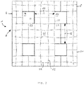
- the compensation effect of the bottom electrodes 8, 12 is indicated with first and second raster lines 23, 24. If the compensation effect of the bottom electrodes 8, 12 were not present, the raster lines 23, 24 would form a uniform raster, the first raster lines 23 in Figure 2 run vertically and parallel to the vertical sections of the edge 21 of the carrier layer 6 and the second raster lines 24 in Figure 2 would run horizontally and would run parallel to the horizontal sections of the edge 21 of the carrier layer 6.
- the raster lines 23, 24 are distorted, so that in the region of the edges 22 of the bottom electrodes 8, 12 in the carrier layer 6 and Base layer 5 form zones 25 with high tensile stress and in the middle of membrane 4 in carrier layer 6 and base layer 5 zones 25 with low tensile stress.
- the membrane 4 remains undamaged during cooling to room temperature. This is achieved by the compensation effect of the bottom electrodes 8, 12.
- the compensation effect originates mainly from the bottom electrodes 8, 12.
- the lead zirconate titanate pixels 9, 13 and the head electrodes 10, 14 make a similar contribution to the compensation effect.
- the contribution of the head electrodes 10, 14 is small compared to the contribution of the lead zirconate titanate pixels 9, 13, since the head electrodes 10, 14 are made very thin due to their semi-transparency , Furthermore, the stress gradients in the membrane 4 are so moderate that the membrane 4 has a high mechanical stability even after cooling.
- the silicon oxide, from which the carrier layer 6 and the base layer 5 are made, advantageously has such a low thermal conductivity that the crosstalk between the individual infrared light sensors 7, 11 is low.
- infrared light sensor chip 1 has an advantageously high signal-to-noise ratio, in particular for frequencies which are lower than the thermal cut-off frequency.
Landscapes
- Spectroscopy & Molecular Physics (AREA)
- Physics & Mathematics (AREA)
- General Physics & Mathematics (AREA)
- Engineering & Computer Science (AREA)
- Nanotechnology (AREA)
- Chemical & Material Sciences (AREA)
- Manufacturing & Machinery (AREA)
- Power Engineering (AREA)
- Photometry And Measurement Of Optical Pulse Characteristics (AREA)
- Micromachines (AREA)
- Physical Vapour Deposition (AREA)
- Formation Of Insulating Films (AREA)
- Solid State Image Pick-Up Elements (AREA)
Description
- Die Erfindung betrifft ein Verfahren zum Herstellen eines Mikrosystems mit Pixel.
- Dünnschichten aus Bleizirkonattitanat (PZT) sind aufgrund ihrer vorteilhaften physikalischen Eigenschaften, wie beispielsweise einer hohen elektromechanischen Kopplung, einer hohen Dielektrizitätszahl oder einem hohen pyroelektrischen Koeffizienten, in der Mikrosystemtechnik weit verbreitet. Ein Mikrosystem weist herkömmlich ein Substrat als einen Träger für die Dünnschicht auf, wobei das Substrat eine Membran aufweist, die von einem Siliziumrahmen aufgespannt ist. Es ist bekannt, die Bleizirkonattitanat-Dünnschicht mit einem Abscheideverfahren, insbesondere einem Sputter-Prozess, auf das Substrat aufzubringen. Eine rasterartige Anordnung von Pixel aus der Dünnschicht wird herkömmlich mit einem fotolithographischen Ätzverfahren erreicht. Die Pixel sind mit Elektroden elektronisch verschaltet, die beispielsweise aus Platin oder einer Chrom-Nickel-Legierung hergestellt sind.
- Patentschrift
US 2013/0023036 A1 offenbart in Figur 9C ein typisches Dünnfilmpixelsystem, das als pyroelektrischer Infrarotsensor mit Goldpixelelektroden verwendet wird, die auf einer Oxid-Doppelschichtmembran ausgebildet sind. - Es ist erforderlich, dass die Membran eine kleine thermische Masse und eine geringe thermische Leitfähigkeit hat, damit thermisches Übersprechen zwischen den Pixel gering ist. Dies wird dadurch erreicht, dass die Membran aus einem schlecht wärmeleitfähigen Material, beispielsweise Siliziumoxid, und möglichst dünn ausgebildet ist. Typischerweise beträgt die Dicke der Membran 1 µm bei einer Rahmenhöhe von 400 µm. Mit Hilfe eines reaktiven Ionentiefenätzverfahrens ist es möglich, die Rückseite des Substrats derart stark anisotrop zu strukturieren, dass Kavitäten ausgebildet werden können. Die Kavitäten erstrecken sich unmittelbar bis zur Membran, so dass diese an ihrer den Pixel abgewandten Seite durch die Kavitäten freigelegt ist. Erstrebenswert ist es die Membran möglichst dünn und mit einer ausreichend hohen Festigkeit herzustellen, damit die Pixel aufgrund geringen Übersprechens eine hohe Funktionalität haben.
- Um die Membran zu stabilisieren ist es bekannt eine zusätzliche Si3N4-Schicht auf dem Substrat vorzusehen. Die zusätzliche Si3N4-Schicht hat jedoch den Nachteil, dass ihre Wärmeleitfähigkeit derart groß ist, dass mit ihr das nachteilige Übersprechen zwischen den einzelnen Pixel erhöht ist. Außerdem erfordert das Herstellen der zusätzlichen Si3N4-Schicht einen weiteren Fertigungsschritt, wodurch höhere Herstellungskosten einhergehen.
- Aufgabe der Erfindung ist es ein Verfahren zur Herstellung eines Mikrosystems mit Pixel zu schaffen, wobei die Pixel eine hohe Funktionalität haben und das Mikrosystem eine hohe mechanische Stabilität hat sowie die Herstellungskosten gering sind.
- Die Aufgabe wird gelöst mit den Merkmalen des unabhängigen Patentanspruchs. Bevorzugte Ausgestaltungen dazu sind in den weiteren Patentansprüchen angegeben.
- Das erfindungsgemäße Verfahren zum Herstellen des Mikrosystems mit den Pixel weist die Schritte auf: Bereitstellen eines Siliziumwafers; Herstellen einer thermischen Siliziumoxidschicht an der Oberfläche des Siliziumwafers als eine Basisschicht mit einer Dicke zwischen 200 nm und 1000 nm durch Oxidation des Siliziumwafers; Herstellen einer Siliziumoxiddünnschicht unmittelbar auf der Basisschicht als eine Trägerschicht mit einer Dicke von 100 nm bis 700 nm durch ein thermisches Abscheideverfahren; Herstellen einer Platinschicht unmittelbar auf der Trägerschicht mit einem thermischen Abscheideverfahren mit einer Dicke von 40 nm bis 200 nm, wodurch ein Zwischenprodukt aufweisend den Siliziumwafer, die Basisschicht, die Trägerschicht und die Platinschicht hergestellt wird; Abkühlen des Zwischenprodukts auf Raumtemperatur; pixelartige Strukturierung der Platinschicht durch Abtragen von überflüssigen Bereichen der Platinschicht, wodurch auf der Trägerschicht von den verbleibenden Bereichen der Platinschicht pixelförmig Bodenelektroden der Pixel ausgebildet werden; Materialabtragung an der der Basisschicht abgewandten Seite des Siliziumwafers, so dass ein Rahmen verbleibt und von dem Rahmen eine Membran gebildet von der Basisschicht und der Trägerschicht aufgespannt wird; Fertigstellen des Mikrosystems.
- Bei der Herstellung des Mikrosystems mit dem erfindungsgemäßen Verfahren ergibt sich das Zwischenprodukt als ein Schichtverbund, der die Basisschicht als die thermische Siliziumoxidschicht mit der Dicke von 200 nm bis 1000 nm, die Trägerschicht als die Siliziumoxiddünnschicht mit der Dicke von 100 nm bis 700 nm und die Platinschicht mit der Dicke von 40 nm bis 200 nm aufweist, wobei die Schichten direkt aneinander liegen und miteinander fest verbunden sind. Nach dem Abkühlen des Zwischenprodukts stellt sich in den Schichten ein entsprechender Spannungszustand ein, der dadurch charakterisiert ist, dass sowohl in der Basisschicht als auch in der Trägerschicht Druckspannungen und in der Platinschicht Zugspannungen vorliegen. Die Druckspannungen in der Trägerschicht sind etwa um fünf- bis zehnmal kleiner als in der Basisschicht und die Zugspannungen in der Platinschicht liegen etwa bei 5 bis 20 MPa. Ferner ist zu beobachten, dass nach der Strukturierung der Platinschicht zu den Platinschichtpixel als die Bodenelektroden in diesen Zugspannungen vorliegen, deren Werte verglichen zu den Zugspannungen in der Platinschicht vor der Strukturierung im Wesentlichen unverändert sind. An den Stellen der Trägerschicht und der Basisschicht, an denen die Platinschichtpixel angeordnet sind, ergibt sich eine Überkompensation der Druckspannungen in der Basisschicht und der Trägerschicht von den Zugspannungen in den Platinschichtpixel derart, dass Zugspannungen und keine Druckspannungen vorliegen. Somit dienen die Platinschichtpixel mit Ihren Zugspannungen zur lokalen Kompensation der Druckspannungen der Basisschicht und der Trägerschicht. Überaschenderweise stellt sich die lokale Kompensation der Druckspannungen der Basisschicht und der Trägerschicht durch die Platinschichtpixel ein, obwohl die Platinschicht nach der Strukturierung der Platinschichtpixel nicht mehr durchgängig auf der Oberfläche vorhanden ist, sondern nur noch in Form der Platinschichtpixel. Die Zugspannungen, die aufgrund der Kompensationswirkung der Platinschichtpixel auf der Trägerschicht und der Basisschicht wirken haben Werte bis etwa 50 MPa.
- Mit Hilfe der erfindungsgemäß in der Membran generierten Spannungszuständen hat die Membran eine hohe Festigkeit, so dass die Membran etwa beim Herstellen des Mikrosystems nicht bricht, obwohl die Membran erfindungsgemäß mit der derart geringen Dicke gebildet ist. Ferner sind die Spannungsgradienten in der Basisschicht und der Trägerschicht derart moderat, dass die Basisschicht und die Trägerschicht eine hohe mechanische Stabilität haben. Außerdem haben die Trägerschicht und die Basisschicht eine derart niedrige Wärmeleitfähigkeit, dass das Übersprechen zwischen den Pixel gering ist. Dadurch hat das Mikrosystem ein vorteilhaft hohes Signal-Rausch-Verhältnis insbesondere für Frequenzen, die kleiner als die thermische Grenzfrequenz sind. Das erfindungsgemäße Verfahren zum Herstellen des Mikrosystems weist Prozessschritte zum Herstellen der Basisschicht und der Trägerschicht auf, wodurch zusätzliche Prozessschritte etwa zum Herstellen einer mechanisch stabilisierenden Si3N4-Schicht nicht notwendig sind. Dadurch sind die Herstellungskosten des erfindungsgemäßen Mikrosystems geringer als für bekannte Mikrosysteme.
- Beforzugtermaßen wird die Platinschicht bei 300 °C bis 550°C gesputtert. Ferner weist das Verfahren bevorzugt den Schritt auf: Herstellen einer Bleizirkonattitanatschicht unmittelbar auf der Platinschichtschicht mit einem thermischen Abscheideverfahren und einer Dicke von 0,2 bis 5 µm, wodurch das Zwischenprodukt die Bleizirkonattitanatschicht aufweist. Hierbei ist es bevorzugt, dass bei der pixelartigen Strukturierung der Platinschicht gleichzeitig die Bleizirkonattitanatschicht durch Abtragen von überflüssigen Bereichen der Bleizirkonattitanatschicht strukturiert wird, wodurch auf den Bodenelektroden von den verbleibenden Bereichen der Bleizirkonattitanatschicht Bleizirkonattitanatpixel der Pixelen ausgebildet werden.
- Das Verfahren weist ferner bevorzugt den Schritt auf: Herstellen einer semitransparenten, elektrisch leitenden Elektrodenschicht unmittelbar auf der Bleizirkonattitanatschicht mit einem thermischen Abscheideverfahren, wodurch das Zwischenprodukt die Elektrodenschicht aufweist. Hierbei ist es bevorzugt, dass die Elektrodenschicht aus Platin oder einer Nickel-Eisen-Verbindung oder einer Nickel-Chrom-Verbindung ist. Bei der pixelartigen Strukturierung der Platinschicht und der Bleizirkonattitanatschicht werden bevorzugt gleichzeitig die Elektrodenschicht durch Abtragen von überflüssigen Bereichen der zweiten Platinschicht strukturiert wird, wodurch auf den Bleizirkonattitanatpixel von den verbleibenden Bereichen der zweiten Platinschicht Kopfelektroden der Pixel ausgebildet werden.
- Außerdem ist es bevorzugt, dass das thermisches Abscheideverfahren ein Sputter-Verfahren ist.
- Im Folgenden wird ein bevorzugtes Ausführungsbeispiel eines mit dem erfindungsgemäßen Verfahren hergestellten Mikrosystems anhand der beigefügten schematischen Zeichnungen erläutert. Es zeigen:
-
Figur 1 eine Querschnittsdarstellung des Ausführungsbeispiels des mit dem erfindungsgemäßen Verfahren hergestellten Mikrosystem und -
Figur 2 eine Draufsicht des Ausführungsbeispiels ausFigur 1 . - Wie es aus
Figuren 1 und2 ersichtlich ist weist ein als ein Mikrosystem hergestellter Infrarotlichtsensorchip 1 ein Substrat 2 auf, das seinerseits einen Rahmen 3 und eine Membran 4 aufweist. Auf dem Rahmen 3 ist die Membran 4 angebracht, so dass von dem Rahmen 3 die Membran 4 abgestützt und aufgespannt ist. Die Membran 4 weist eine Basisschicht 5, die eine thermische Siliziumoxidschicht ist, und eine Trägerschicht 6 auf, die eine Siliziumoxiddünnschicht ist. - Auf der Trägerschicht 6 sind ein erster Infrarotlichtsensor 7 mit einer ersten Bodenelektrode 8 aus Platin, einem ersten Bleizirkonattitanatpixel 9 mit einem hohen Anteil an Zirkon und einer ersten Kopfelektrode 10 aus Platin sowie ein zweiter Infrarotlichtsensor 11 mit einer zweiten Bodenelektrode 8 aus Platin, einem zweiten Bleizirkonattitanatpixel 9 mit einem hohen Anteil an Zirkon und einer zweiten Kopfelektrode 10 aus Platin angeordnet. Die Bleizirkonattitanatpixel 9, 13 sind jeweils zwischen ihren Bodenelkroden 8, 12 und ihren Kopfelektroden 10, 14 angeordnet, wobei die Bodenelektroden 8, 12 direkt auf der Trägerschicht 6 angeordnet sind.
- Die Kopfelektroden 10, 14 sind semitransparent ausgebildet, so dass Infrarotlicht von außen auf die Bleizirkonattitanatpixel 9, 13 treffen kann. Der Abstand 15 zwischen den Infrarotlichtsensoren 7, 11 ist derart groß gewählt, dass das Übersprechen zwischen den Infrarotlichtsensoren 7, 11 innerhalb eines noch zulässigen Ausmaßes ist. Die Basisschicht 5 hat eine Dicke 16 zwischen 200 nm und 1000 nm und die Trägerschicht 6 hat eine Dicke 17 von 100 nm bis 700 nm, wohingegen die Bodenelektroden 8, 12 eine Dicke 18 von 40 nm bis 200 nm haben. Die Bleizirkonattitanatpixel 9, 13 haben eine Dicke 19 von wenigen Mikrometern, insbesondere von 2 bis 5 µm. Die Kopfelektroden 10, 14 haben eine Dicke 20 von 3 bis 200 nm.
- Zum Herstellen des Infrarotlichtsensorchips sind folgende Schritte durchzuführen: Die thermische Siliziumoxidschicht wird an der Oberfläche eines Siliziumwafers als die Basisschicht 5 mit der Dicke 16 durch Oxidation des Siliziumwafers hergestellt. Ferner wird die Siliziumoxiddünnschicht unmittelbar auf der Basisschicht 5 als die Trägerschicht 6 mit der Dicke 17 durch ein thermisches Abscheideverfahren hergestellt. Eine Platinschicht wird danach unmittelbar auf die Trägerschicht 17 mit der Dicke 18 bei 300 °C bis 550°C gesputtert. Anschließend wird eine Bleizirkonattitanatschicht unmittelbar auf die Platinschichtschicht mit einem thermischen Abscheideverfahren und der Dicke 19 aufgebracht. Unmittelbar auf die Bleizirkonattitanatschicht wird anschließend eine semitransparente, elektrisch leitende Elektrodenschicht aus Platin oder einer Nickel-Eisen-Verbindung oder einer Nickel-Chrom-Verbindung mit einem thermischen Abscheideverfahren und der Dicke 20 aufgebracht.
- Anschließend wird der Siliziumwafer mit der Basisschicht 5, der Trägerschicht 6, der Platinschicht, der Bleizirkonattitanatschicht und der Elektrodenschicht auf Raumtemperatur abgekühlt. Alternativ ist denkbar die Elektrodenschicht erst nach der Abkühlung auf die Bleizirkonattitanatschicht aufzubringen. Nach dem Abkühlen stellen sich sowohl in der Basisschicht 5 als auch in der Trägerschicht 6 Druckspannungen und in der Platinschicht Zugspannungen ein. Die Druckspannungen in der Trägerschicht 6 sind etwa um fünf- bis zehnmal kleiner als in der Basisschicht 5 und die Zugspannungen in der Platinschicht liegen etwa bei 5 bis 20 MPa.
- Es wird ferner eine pixelartige Strukturierung vorgenommen, wobei überflüssige Bereiche der Platinschicht, der Bleizirkonattitanatschicht und der Elektrodenschicht abgetragen werden, so dass die Infrarotlichtsensoren 7, 11 im Abstand 15 zueinander herausgearbeitet werden. Schließlich wird durch Materialabtragung an der der Basisschicht abgewandten Seite des Siliziumwafers eine Aussparung hergestellt, so dass vom Siliziumwafer der Rahmen 3 verbleibt, von dem die Membran 4 gebildet von der Basisschicht 5 und der Trägerschicht 6 aufgespannt wird.
- Nach der pixelartigen Strukturierung liegen in den Bodenelektroden 8, 12 Zugspannungen vor, deren Werte verglichen zu den Zugspannungen in der Platinschicht vor der Strukturierung im Wesentlichen unverändert sind. An den Stellen der Trägerschicht 6 und der Basisschicht 5, an denen die Bodenelektroden 8, 12 angeordnet sind, ergibt sich eine Überkompensation der Druckspannungen in der Basisschicht 5 und der Trägerschicht 6 von den Zugspannungen in den Bodenelektroden 8, 12 derart, dass Zugspannungen und keine Druckspannungen vorliegen. Somit dienen die Bodenelektroden 60 12 mit ihren Zugspannungen zur lokalen Kompensation der Druckspannungen der Basisschicht 5 und der Trägerschicht 6. Es stellt sich die lokale Kompensation der Druckspannungen der Basisschicht 5 und der Trägerschicht 6 durch die Bodenelektroden 8, 12 ein, obwohl die Platinschicht nach der Strukturierung des Infrarotlichtsensors nicht mehr durchgängig auf der Oberfläche der Trägerschicht 6 vorhanden ist. Die Zugspannungen, die aufgrund der Kompensationswirkung der Bodenelektroden 8, 12 auf der Trägerschicht 6 und der Basisschicht 5 wirken haben Werte bis etwa 50 MPa.
- In
Figur 2 ist die Kompensationswirkung der Bodenelektroden 8, 12 mit ersten und zweiten Rasterlinien 23, 24 angedeutet. Wäre die Kompensationswirkung der Bodenelektroden 8, 12 nicht vorhanden, würden die Raserlinien 23, 24 ein gleichmäßiges Raster bilden, wobei die ersten Rasterlinien 23 inFigur 2 senkrecht verlaufen und zu den senkrechten Abschnitten des Rands 21 der Trägerschicht 6 parallel und die zweiten Rasterlinien 24 inFigur 2 waagrecht verlaufen und zu den waagerechten Abschnitten des Rands 21 der Trägerschicht 6 parallel verlaufen würden. - Aufgrund der Überlagerung der Zugspannungen in den Bodenelektroden 8, 12 mit den Druckspannungen in der Trägerschicht 6 und der Basisschicht 5 ergibt sich eine Verzerrung der Rasterlinien 23, 24, so dass im Bereich der Ränder 22 der Bodenelektroden 8, 12 in der Trägerschicht 6 und der Basisschicht 5 Zonen 25 mit hoher Zugspannung und in der Mitte der Membran 4 in der Trägerschicht 6 und der Basisschicht 5 Zonen 25 mit niedriger Zugspannung ausbilden.
- Obwohl die Basisschicht 5 und die Trägerschicht derart dünn ausgebildet sind, bleibt die Membran 4 während des Abkühlens auf die Raumtemperatur unbeschädigt. Dies wird durch die Kompensationswirkung der Bodenelektroden 8, 12 erzielt. Die Kompensationswirkung geht hauptsächlich von den Bodenelektroden 8, 12 aus. Einen Beitrag zur Kompensationswirkung leisten analog die Bleizirkonattitanatpixel 9, 13 und die Kopfelektroden 10, 14. Der Beitrag der Kopfelektroden 10, 14 ist klein verglichen mit dem Beitrag der Bleizirkonattitanatpixel 9, 13, da die Kopfelektroden 10, 14 aufgrund ihrer Semitransparenz sehr dünn ausgeführt sind. Ferner sind die Spannungsgradienten in der Membran 4 derart moderat, dass die Membran 4 auch nach der Abkühlung eine hohe mechanische Stabilität hat. Das Siliziumoxid, aus dem die Trägerschicht 6 und die Basisschicht 5 sind, hat vorteilhaft eine derart niedrige Wärmeleitfähigkeit, dass das Übersprechen zwischen den einzelnen Infrarotlichtsensoren 7, 11 gering ist. Dadurch hat Infrarotlichtsensorchip 1 ein vorteilhaft hohes Signal-Rasch-Verhältnis insbesondere für Frequenzen, die kleiner als die thermische Grenzfrequenz sind.
-
- 1
- Pixelchip
- 2
- Substrat
- 3
- Rahmen
- 4
- Membran
- 5
- Basisschicht
- 6
- Trägerschicht
- 7
- erstes Pixel
- 8
- erste Bodenelektrode
- 9
- erste Bleizirkonattitanatpixel
- 10
- erste Kopfelektrode
- 11
- zweites Pixel
- 12
- zweite Bodenelektrode
- 13
- zweite Bleizirkonattitanatpixel
- 14
- zweite Kopfelektrode
- 15
- Abstand zwischen den Pixel
- 16
- Dicke der Basisschicht
- 17
- Dicke der Trägerschicht
- 18
- Dicke der Bodenelektrode
- 19
- Dicke der Bleizirkonattitanatpixel
- 20
- Dicke der Kopfelektrode
- 21
- Rand der Trägerschicht
- 22
- Rand der Bodenelektrode
- 23
- erste Rasterlinie
- 24
- zweite Rasterlinie
- 25
- Zone mit hoher Zugspannung
- 26
- Zone mit niedriger Zugspannung
Claims (8)
- Verfahren zum Herstellen eines Mikrosystems (1) mit Pixel, aufweisend die Schritte:- Bereitstellen eines Siliziumwafers;- Herstellen einer thermischen Siliziumoxidschicht an der Oberfläche des Siliziumwafers als eine Basisschicht (5) mit einer Dicke zwischen 200 nm und 1000 nm durch Oxidation des Siliziumwafers;- Herstellen einer Siliziumoxiddünnschicht unmittelbar auf der Basisschicht (5) als eine Trägerschicht (6) mit einer Dicke von 100 nm bis 700 nm durch ein thermisches Abscheideverfahren;- Herstellen einer Platinschicht unmittelbar auf der Trägerschicht (6) mit einem thermischen Abscheideverfahren mit einer Dicke von 40 nm bis 200 nm, wodurch ein Zwischenprodukt aufweisend den Siliziumwafer, die Basisschicht (5), die Trägerschicht (6) und die Platinschicht hergestellt wird;- Abkühlen des Zwischenprodukts auf Raumtemperatur;- pixelartige Strukturierung der Platinschicht durch Abtragen von überflüssigen Bereichen der Platinschicht, wodurch auf der Trägerschicht (6) von den verbleibenden Bereichen der Platinschicht pixelförmig Bodenelektroden (8, 12) der Pixel (7, 8) ausgebildet werden;- Materialabtragung an der der Basisschicht (5) abgewandten Seite des Siliziumwafers, so dass ein Rahmen (3) verbleibt und von dem Rahmen (3) eine Membran (4) gebildet von der Basisschicht (5) und der Trägerschicht (6) aufgespannt wird;- Fertigstellen des Mikrosystems (1).
- Vefahren gemäß Anspruch 1, wobei die Platinschicht bei 300 °C bis 550°C gesputtert wird.
- Vefahren gemäß Anspruch 1 oder 2, wobei das Verfahren den Schritt aufweist: Herstellen einer Bleizirkonattitanatschicht unmittelbar auf der Platinschichtschicht mit einem thermischen Abscheideverfahren und einer Dicke von 0,2 bis 5 µm, wodurch das Zwischenprodukt die Bleizirkonattitanatschicht aufweist.
- Verfahren gemäß Anspruch 3, wobei bei der pixelartigen Strukturierung der Platinschicht gleichzeitig die Bleizirkonattitanatschicht durch Abtragen von überflüssigen Bereichen der Bleizirkonattitanatschicht strukturiert wird, wodurch auf den Bodenelektroden (8, 12) von den verbleibenden Bereichen der Bleizirkonattitanatschicht Bleizirkonattitanatpixel (9, 13) der Pixelen (7, 11) ausgebildet werden.
- Verfahren gemäß einem der Ansprüche 3 bis 4, wobei das Verfahren den Schritt aufweist: Herstellen einer semitransparenten, elektrisch leitenden Elektrodenschicht unmittelbar auf der Bleizirkonattitanatschicht mit einem thermischen Abscheideverfahren, wodurch das Zwischenprodukt die Elektrodenschicht aufweist.
- Verfahren gemäß Anspruch 5, wobei die Elektrodenschicht aus Platin oder einer Nickel-Eisen-Verbindung oder einer Nickel-Chrom-Verbindung ist.
- Verfahren gemäß Anspruch 6, wobei bei der pixelartigen Strukturierung der Platinschicht und der Bleizirkonattitanatschicht gleichzeitig die Elektrodenschicht durch Abtragen von überflüssigen Bereichen der zweiten Platinschicht strukturiert wird, wodurch auf den Bleizirkonattitanatpixel (9, 13) von den verbleibenden Bereichen der zweiten Platinschicht Kopfelektroden (10, 14) der Pixel (7, 11) ausgebildet werden.
- Verfahren gemäß einem der Ansprüche 1 bis 7, wobei das thermische Abscheideverfahren ein Sputter-Verfahren ist.
Applications Claiming Priority (2)
| Application Number | Priority Date | Filing Date | Title |
|---|---|---|---|
| DE201310108280 DE102013108280B3 (de) | 2013-08-01 | 2013-08-01 | Verfahren zum Herstellen eines Mikrosystems mit Pixel |
| PCT/EP2014/066084 WO2015014754A2 (de) | 2013-08-01 | 2014-07-25 | Verfahren zum herstellen eines mikrosystems mit pixel |
Publications (2)
| Publication Number | Publication Date |
|---|---|
| EP3028021A2 EP3028021A2 (de) | 2016-06-08 |
| EP3028021B1 true EP3028021B1 (de) | 2020-02-12 |
Family
ID=51228437
Family Applications (1)
| Application Number | Title | Priority Date | Filing Date |
|---|---|---|---|
| EP14744323.8A Active EP3028021B1 (de) | 2013-08-01 | 2014-07-25 | Verfahren zum herstellen eines mikrosystems mit pixel |
Country Status (7)
| Country | Link |
|---|---|
| US (1) | US9842959B2 (de) |
| EP (1) | EP3028021B1 (de) |
| JP (1) | JP6429873B2 (de) |
| KR (1) | KR20160040636A (de) |
| CN (1) | CN105593653A (de) |
| DE (1) | DE102013108280B3 (de) |
| WO (1) | WO2015014754A2 (de) |
Family Cites Families (13)
| Publication number | Priority date | Publication date | Assignee | Title |
|---|---|---|---|---|
| GB2116363B (en) * | 1982-03-03 | 1985-10-16 | Philips Electronic Associated | Multi-level infra-red detectors and their manufacture |
| JP2748953B2 (ja) * | 1993-12-13 | 1998-05-13 | 日本電気株式会社 | 熱型赤外線センサ |
| DE19525071A1 (de) * | 1995-07-10 | 1997-01-16 | Siemens Ag | Pyroelektrisches Bauelement und Verfahren zur Herstellung |
| JP4612932B2 (ja) * | 2000-06-01 | 2011-01-12 | ホーチキ株式会社 | 赤外線検出素子および赤外線2次元イメージセンサ |
| DE10103529B4 (de) * | 2001-01-26 | 2004-01-15 | Siemens Ag | Ferroelektrischer Kondensator, Verfahren zur Herstellung und Verwendung des Kondensators |
| WO2004051760A1 (ja) * | 2002-12-05 | 2004-06-17 | Matsushita Electric Industrial Co., Ltd. | 焦電体素子及びその製造方法並びに赤外線センサ |
| CN1692504A (zh) * | 2002-12-05 | 2005-11-02 | 松下电器产业株式会社 | 热电器件及其制造方法与红外线传感器 |
| JP4926596B2 (ja) * | 2006-08-08 | 2012-05-09 | スタンレー電気株式会社 | 光偏向器及びその製造方法 |
| DE102007046451B4 (de) * | 2007-09-28 | 2011-08-25 | Pyreos Ltd. | Vorrichtung zur Detektion von Wärmestrahlung mit hoher Auflösung, Verfahren zum Herstellen und Verwendung der Vorrichtung |
| US8513042B2 (en) * | 2009-06-29 | 2013-08-20 | Freescale Semiconductor, Inc. | Method of forming an electromechanical transducer device |
| EP2528698A1 (de) * | 2010-01-29 | 2012-12-05 | Research Triangle Institute | Verfahren zur formung piezoelektrischer ultraschallsondenköpfe und entsprechende vorrichtungen |
| JP5399970B2 (ja) * | 2010-03-31 | 2014-01-29 | パナソニック株式会社 | 強誘電体デバイスの製造方法 |
| JP5533638B2 (ja) * | 2010-12-24 | 2014-06-25 | セイコーエプソン株式会社 | 検出装置、センサーデバイス及び電子機器 |
-
2013
- 2013-08-01 DE DE201310108280 patent/DE102013108280B3/de active Active
-
2014
- 2014-07-25 CN CN201480054691.1A patent/CN105593653A/zh active Pending
- 2014-07-25 JP JP2016530460A patent/JP6429873B2/ja not_active Expired - Fee Related
- 2014-07-25 KR KR1020167005474A patent/KR20160040636A/ko not_active Withdrawn
- 2014-07-25 EP EP14744323.8A patent/EP3028021B1/de active Active
- 2014-07-25 WO PCT/EP2014/066084 patent/WO2015014754A2/de not_active Ceased
-
2016
- 2016-02-01 US US15/011,812 patent/US9842959B2/en active Active
Non-Patent Citations (1)
| Title |
|---|
| None * |
Also Published As
| Publication number | Publication date |
|---|---|
| CN105593653A (zh) | 2016-05-18 |
| US20160149071A1 (en) | 2016-05-26 |
| WO2015014754A3 (de) | 2015-04-02 |
| KR20160040636A (ko) | 2016-04-14 |
| EP3028021A2 (de) | 2016-06-08 |
| WO2015014754A2 (de) | 2015-02-05 |
| US9842959B2 (en) | 2017-12-12 |
| JP2016532864A (ja) | 2016-10-20 |
| JP6429873B2 (ja) | 2018-11-28 |
| DE102013108280B3 (de) | 2014-10-09 |
Similar Documents
| Publication | Publication Date | Title |
|---|---|---|
| DE60214683T2 (de) | Platten aus refraktärem metall mit einheitlicher textur und verfahren zu ihrer herstellung | |
| DE4315012B4 (de) | Verfahren zur Herstellung von Sensoren und Sensor | |
| DE10055421A1 (de) | Verfahren zur Erzeugung einer mikromechanischen Struktur und mikromechanische Struktur | |
| WO2007082662A1 (de) | Mems-sensor mit deformationsfreier rückelektrode | |
| WO2009092584A1 (de) | Piezoelektrisches vielschichtbauelement | |
| DE102009025413A1 (de) | Vorrichtung, die eine Imidschicht mit Nichtkontaktöffnung umfasst, und Verfahren | |
| EP3526158B1 (de) | Verfahren zum herstellen eines stressentkoppelten mikromechanischen drucksensors | |
| DE102020214925A1 (de) | Verfahren zur Herstellung eines Polysilizium-SOI-Substrats mit einer Kavität | |
| EP0628209B1 (de) | Verfahren zum herstellen eines druckdifferenz-sensors | |
| EP2019812B1 (de) | Verfahren zur herstellung eines mikromechanischen bauelements mit membran und mikromechanisches bauelement | |
| EP2285733B1 (de) | Verfahren zur herstellung von chips | |
| DE102013108280B3 (de) | Verfahren zum Herstellen eines Mikrosystems mit Pixel | |
| DE102006022377B4 (de) | Mikromechanische Vorrichtung und Verfahren zur Herstellung einer mikromechanischen Vorrichtung | |
| DE102007026450A1 (de) | Sensor mit Nut zur mechanischen Stress Reduzierung und Verfahren zur Herstellung des Sensors | |
| DE112017007299T5 (de) | Halbleiterelement-bonding-körper, halbleitereinheit und verfahren zur herstellung eines halbleiterelement-bonding-körpers | |
| DE102012106431B4 (de) | Elektronisches Bauteil und Verfahren zu seiner Herstellung | |
| WO2010054875A1 (de) | Anordnung von mindestens zwei wafern mit einer bondverbindung und verfahren zur herstellung einer solchen anordnung | |
| EP2714582B1 (de) | Verfahren zur herstellung eines mos-transistors | |
| DE19710375C2 (de) | Verfahren zum Herstellen von räumlich strukturierten Bauteilen | |
| WO2007000363A1 (de) | Verfahren zur herstellung eines mikromechanischen bauelements sowie mikromechanisches bauelement | |
| DE102017003698B3 (de) | Herstellung einer dünnen Substratschicht | |
| EP4564849A1 (de) | Mems-wandler mit zumindest einer metall- und einer oxidschicht | |
| WO2018114634A1 (de) | Piezoelektrischer stapelaktuator und verfahren zur herstellung desselben | |
| DE102018111200A1 (de) | Verfahren zur Herstellung eines wenigstens teilweise gehäusten Halbleiterwafers | |
| EP4564850A1 (de) | Mems-wandler mit einer trägerschicht und zumindest zwei piezoschichten |
Legal Events
| Date | Code | Title | Description |
|---|---|---|---|
| PUAI | Public reference made under article 153(3) epc to a published international application that has entered the european phase |
Free format text: ORIGINAL CODE: 0009012 |
|
| 17P | Request for examination filed |
Effective date: 20160219 |
|
| AK | Designated contracting states |
Kind code of ref document: A2 Designated state(s): AL AT BE BG CH CY CZ DE DK EE ES FI FR GB GR HR HU IE IS IT LI LT LU LV MC MK MT NL NO PL PT RO RS SE SI SK SM TR |
|
| AX | Request for extension of the european patent |
Extension state: BA ME |
|
| DAX | Request for extension of the european patent (deleted) | ||
| GRAJ | Information related to disapproval of communication of intention to grant by the applicant or resumption of examination proceedings by the epo deleted |
Free format text: ORIGINAL CODE: EPIDOSDIGR1 |
|
| GRAP | Despatch of communication of intention to grant a patent |
Free format text: ORIGINAL CODE: EPIDOSNIGR1 |
|
| STAA | Information on the status of an ep patent application or granted ep patent |
Free format text: STATUS: REQUEST FOR EXAMINATION WAS MADE |
|
| GRAP | Despatch of communication of intention to grant a patent |
Free format text: ORIGINAL CODE: EPIDOSNIGR1 |
|
| STAA | Information on the status of an ep patent application or granted ep patent |
Free format text: STATUS: GRANT OF PATENT IS INTENDED |
|
| GRAJ | Information related to disapproval of communication of intention to grant by the applicant or resumption of examination proceedings by the epo deleted |
Free format text: ORIGINAL CODE: EPIDOSDIGR1 |
|
| GRAP | Despatch of communication of intention to grant a patent |
Free format text: ORIGINAL CODE: EPIDOSNIGR1 |
|
| INTG | Intention to grant announced |
Effective date: 20190802 |
|
| INTG | Intention to grant announced |
Effective date: 20190808 |
|
| INTG | Intention to grant announced |
Effective date: 20190827 |
|
| GRAS | Grant fee paid |
Free format text: ORIGINAL CODE: EPIDOSNIGR3 |
|
| GRAA | (expected) grant |
Free format text: ORIGINAL CODE: 0009210 |
|
| STAA | Information on the status of an ep patent application or granted ep patent |
Free format text: STATUS: THE PATENT HAS BEEN GRANTED |
|
| AK | Designated contracting states |
Kind code of ref document: B1 Designated state(s): AL AT BE BG CH CY CZ DE DK EE ES FI FR GB GR HR HU IE IS IT LI LT LU LV MC MK MT NL NO PL PT RO RS SE SI SK SM TR |
|
| REG | Reference to a national code |
Ref country code: GB Ref legal event code: FG4D Free format text: NOT ENGLISH |
|
| REG | Reference to a national code |
Ref country code: CH Ref legal event code: EP |
|
| REG | Reference to a national code |
Ref country code: AT Ref legal event code: REF Ref document number: 1232747 Country of ref document: AT Kind code of ref document: T Effective date: 20200215 |
|
| REG | Reference to a national code |
Ref country code: IE Ref legal event code: FG4D Free format text: LANGUAGE OF EP DOCUMENT: GERMAN |
|
| REG | Reference to a national code |
Ref country code: DE Ref legal event code: R096 Ref document number: 502014013609 Country of ref document: DE |
|
| PG25 | Lapsed in a contracting state [announced via postgrant information from national office to epo] |
Ref country code: NO Free format text: LAPSE BECAUSE OF FAILURE TO SUBMIT A TRANSLATION OF THE DESCRIPTION OR TO PAY THE FEE WITHIN THE PRESCRIBED TIME-LIMIT Effective date: 20200512 Ref country code: RS Free format text: LAPSE BECAUSE OF FAILURE TO SUBMIT A TRANSLATION OF THE DESCRIPTION OR TO PAY THE FEE WITHIN THE PRESCRIBED TIME-LIMIT Effective date: 20200212 Ref country code: FI Free format text: LAPSE BECAUSE OF FAILURE TO SUBMIT A TRANSLATION OF THE DESCRIPTION OR TO PAY THE FEE WITHIN THE PRESCRIBED TIME-LIMIT Effective date: 20200212 |
|
| REG | Reference to a national code |
Ref country code: LT Ref legal event code: MG4D |
|
| REG | Reference to a national code |
Ref country code: NL Ref legal event code: MP Effective date: 20200212 |
|
| PG25 | Lapsed in a contracting state [announced via postgrant information from national office to epo] |
Ref country code: HR Free format text: LAPSE BECAUSE OF FAILURE TO SUBMIT A TRANSLATION OF THE DESCRIPTION OR TO PAY THE FEE WITHIN THE PRESCRIBED TIME-LIMIT Effective date: 20200212 Ref country code: GR Free format text: LAPSE BECAUSE OF FAILURE TO SUBMIT A TRANSLATION OF THE DESCRIPTION OR TO PAY THE FEE WITHIN THE PRESCRIBED TIME-LIMIT Effective date: 20200513 Ref country code: LV Free format text: LAPSE BECAUSE OF FAILURE TO SUBMIT A TRANSLATION OF THE DESCRIPTION OR TO PAY THE FEE WITHIN THE PRESCRIBED TIME-LIMIT Effective date: 20200212 Ref country code: SE Free format text: LAPSE BECAUSE OF FAILURE TO SUBMIT A TRANSLATION OF THE DESCRIPTION OR TO PAY THE FEE WITHIN THE PRESCRIBED TIME-LIMIT Effective date: 20200212 Ref country code: BG Free format text: LAPSE BECAUSE OF FAILURE TO SUBMIT A TRANSLATION OF THE DESCRIPTION OR TO PAY THE FEE WITHIN THE PRESCRIBED TIME-LIMIT Effective date: 20200512 Ref country code: IS Free format text: LAPSE BECAUSE OF FAILURE TO SUBMIT A TRANSLATION OF THE DESCRIPTION OR TO PAY THE FEE WITHIN THE PRESCRIBED TIME-LIMIT Effective date: 20200612 |
|
| PG25 | Lapsed in a contracting state [announced via postgrant information from national office to epo] |
Ref country code: NL Free format text: LAPSE BECAUSE OF FAILURE TO SUBMIT A TRANSLATION OF THE DESCRIPTION OR TO PAY THE FEE WITHIN THE PRESCRIBED TIME-LIMIT Effective date: 20200212 |
|
| PG25 | Lapsed in a contracting state [announced via postgrant information from national office to epo] |
Ref country code: RO Free format text: LAPSE BECAUSE OF FAILURE TO SUBMIT A TRANSLATION OF THE DESCRIPTION OR TO PAY THE FEE WITHIN THE PRESCRIBED TIME-LIMIT Effective date: 20200212 Ref country code: CZ Free format text: LAPSE BECAUSE OF FAILURE TO SUBMIT A TRANSLATION OF THE DESCRIPTION OR TO PAY THE FEE WITHIN THE PRESCRIBED TIME-LIMIT Effective date: 20200212 Ref country code: LT Free format text: LAPSE BECAUSE OF FAILURE TO SUBMIT A TRANSLATION OF THE DESCRIPTION OR TO PAY THE FEE WITHIN THE PRESCRIBED TIME-LIMIT Effective date: 20200212 Ref country code: EE Free format text: LAPSE BECAUSE OF FAILURE TO SUBMIT A TRANSLATION OF THE DESCRIPTION OR TO PAY THE FEE WITHIN THE PRESCRIBED TIME-LIMIT Effective date: 20200212 Ref country code: SM Free format text: LAPSE BECAUSE OF FAILURE TO SUBMIT A TRANSLATION OF THE DESCRIPTION OR TO PAY THE FEE WITHIN THE PRESCRIBED TIME-LIMIT Effective date: 20200212 Ref country code: SK Free format text: LAPSE BECAUSE OF FAILURE TO SUBMIT A TRANSLATION OF THE DESCRIPTION OR TO PAY THE FEE WITHIN THE PRESCRIBED TIME-LIMIT Effective date: 20200212 Ref country code: DK Free format text: LAPSE BECAUSE OF FAILURE TO SUBMIT A TRANSLATION OF THE DESCRIPTION OR TO PAY THE FEE WITHIN THE PRESCRIBED TIME-LIMIT Effective date: 20200212 Ref country code: ES Free format text: LAPSE BECAUSE OF FAILURE TO SUBMIT A TRANSLATION OF THE DESCRIPTION OR TO PAY THE FEE WITHIN THE PRESCRIBED TIME-LIMIT Effective date: 20200212 Ref country code: PT Free format text: LAPSE BECAUSE OF FAILURE TO SUBMIT A TRANSLATION OF THE DESCRIPTION OR TO PAY THE FEE WITHIN THE PRESCRIBED TIME-LIMIT Effective date: 20200705 |
|
| REG | Reference to a national code |
Ref country code: DE Ref legal event code: R097 Ref document number: 502014013609 Country of ref document: DE |
|
| PLBE | No opposition filed within time limit |
Free format text: ORIGINAL CODE: 0009261 |
|
| STAA | Information on the status of an ep patent application or granted ep patent |
Free format text: STATUS: NO OPPOSITION FILED WITHIN TIME LIMIT |
|
| 26N | No opposition filed |
Effective date: 20201113 |
|
| PG25 | Lapsed in a contracting state [announced via postgrant information from national office to epo] |
Ref country code: IT Free format text: LAPSE BECAUSE OF FAILURE TO SUBMIT A TRANSLATION OF THE DESCRIPTION OR TO PAY THE FEE WITHIN THE PRESCRIBED TIME-LIMIT Effective date: 20200212 |
|
| PG25 | Lapsed in a contracting state [announced via postgrant information from national office to epo] |
Ref country code: MC Free format text: LAPSE BECAUSE OF FAILURE TO SUBMIT A TRANSLATION OF THE DESCRIPTION OR TO PAY THE FEE WITHIN THE PRESCRIBED TIME-LIMIT Effective date: 20200212 Ref country code: PL Free format text: LAPSE BECAUSE OF FAILURE TO SUBMIT A TRANSLATION OF THE DESCRIPTION OR TO PAY THE FEE WITHIN THE PRESCRIBED TIME-LIMIT Effective date: 20200212 Ref country code: SI Free format text: LAPSE BECAUSE OF FAILURE TO SUBMIT A TRANSLATION OF THE DESCRIPTION OR TO PAY THE FEE WITHIN THE PRESCRIBED TIME-LIMIT Effective date: 20200212 |
|
| REG | Reference to a national code |
Ref country code: CH Ref legal event code: PL |
|
| REG | Reference to a national code |
Ref country code: BE Ref legal event code: MM Effective date: 20200731 |
|
| PG25 | Lapsed in a contracting state [announced via postgrant information from national office to epo] |
Ref country code: LU Free format text: LAPSE BECAUSE OF NON-PAYMENT OF DUE FEES Effective date: 20200725 Ref country code: FR Free format text: LAPSE BECAUSE OF NON-PAYMENT OF DUE FEES Effective date: 20200731 Ref country code: LI Free format text: LAPSE BECAUSE OF NON-PAYMENT OF DUE FEES Effective date: 20200731 Ref country code: CH Free format text: LAPSE BECAUSE OF NON-PAYMENT OF DUE FEES Effective date: 20200731 |
|
| PG25 | Lapsed in a contracting state [announced via postgrant information from national office to epo] |
Ref country code: BE Free format text: LAPSE BECAUSE OF NON-PAYMENT OF DUE FEES Effective date: 20200731 |
|
| PG25 | Lapsed in a contracting state [announced via postgrant information from national office to epo] |
Ref country code: IE Free format text: LAPSE BECAUSE OF NON-PAYMENT OF DUE FEES Effective date: 20200725 |
|
| REG | Reference to a national code |
Ref country code: AT Ref legal event code: MM01 Ref document number: 1232747 Country of ref document: AT Kind code of ref document: T Effective date: 20200725 |
|
| PG25 | Lapsed in a contracting state [announced via postgrant information from national office to epo] |
Ref country code: AT Free format text: LAPSE BECAUSE OF NON-PAYMENT OF DUE FEES Effective date: 20200725 |
|
| PG25 | Lapsed in a contracting state [announced via postgrant information from national office to epo] |
Ref country code: TR Free format text: LAPSE BECAUSE OF FAILURE TO SUBMIT A TRANSLATION OF THE DESCRIPTION OR TO PAY THE FEE WITHIN THE PRESCRIBED TIME-LIMIT Effective date: 20200212 Ref country code: MT Free format text: LAPSE BECAUSE OF FAILURE TO SUBMIT A TRANSLATION OF THE DESCRIPTION OR TO PAY THE FEE WITHIN THE PRESCRIBED TIME-LIMIT Effective date: 20200212 Ref country code: CY Free format text: LAPSE BECAUSE OF FAILURE TO SUBMIT A TRANSLATION OF THE DESCRIPTION OR TO PAY THE FEE WITHIN THE PRESCRIBED TIME-LIMIT Effective date: 20200212 |
|
| PG25 | Lapsed in a contracting state [announced via postgrant information from national office to epo] |
Ref country code: MK Free format text: LAPSE BECAUSE OF FAILURE TO SUBMIT A TRANSLATION OF THE DESCRIPTION OR TO PAY THE FEE WITHIN THE PRESCRIBED TIME-LIMIT Effective date: 20200212 Ref country code: AL Free format text: LAPSE BECAUSE OF FAILURE TO SUBMIT A TRANSLATION OF THE DESCRIPTION OR TO PAY THE FEE WITHIN THE PRESCRIBED TIME-LIMIT Effective date: 20200212 |
|
| REG | Reference to a national code |
Ref country code: DE Ref legal event code: R082 Ref document number: 502014013609 Country of ref document: DE Representative=s name: DILG, HAEUSLER, SCHINDELMANN PATENTANWALTSGESE, DE |
|
| REG | Reference to a national code |
Ref country code: DE Ref legal event code: R081 Ref document number: 502014013609 Country of ref document: DE Owner name: AVAGO TECHNOLOGIES INTERNATIONAL SALES PTE. LT, SG Free format text: FORMER OWNER: PYREOS LTD., EDINBURGH, GB |
|
| PGFP | Annual fee paid to national office [announced via postgrant information from national office to epo] |
Ref country code: GB Payment date: 20250619 Year of fee payment: 12 |
|
| PGFP | Annual fee paid to national office [announced via postgrant information from national office to epo] |
Ref country code: DE Payment date: 20250710 Year of fee payment: 12 |