EP3015426B1 - Graphenschicht, verfahren zur formung davon, vorrichtung mit der graphenschicht und verfahren zur herstellung der vorrichtung - Google Patents
Graphenschicht, verfahren zur formung davon, vorrichtung mit der graphenschicht und verfahren zur herstellung der vorrichtung Download PDFInfo
- Publication number
- EP3015426B1 EP3015426B1 EP15192138.4A EP15192138A EP3015426B1 EP 3015426 B1 EP3015426 B1 EP 3015426B1 EP 15192138 A EP15192138 A EP 15192138A EP 3015426 B1 EP3015426 B1 EP 3015426B1
- Authority
- EP
- European Patent Office
- Prior art keywords
- graphene
- type
- layer
- source gas
- atoms
- Prior art date
- Legal status (The legal status is an assumption and is not a legal conclusion. Google has not performed a legal analysis and makes no representation as to the accuracy of the status listed.)
- Active
Links
Images











Classifications
-
- C—CHEMISTRY; METALLURGY
- C01—INORGANIC CHEMISTRY
- C01B—NON-METALLIC ELEMENTS; COMPOUNDS THEREOF; METALLOIDS OR COMPOUNDS THEREOF NOT COVERED BY SUBCLASS C01C
- C01B32/00—Carbon; Compounds thereof
- C01B32/15—Nano-sized carbon materials
- C01B32/182—Graphene
- C01B32/184—Preparation
- C01B32/186—Preparation by chemical vapour deposition [CVD]
-
- H—ELECTRICITY
- H10—SEMICONDUCTOR DEVICES; ELECTRIC SOLID-STATE DEVICES NOT OTHERWISE PROVIDED FOR
- H10D—INORGANIC ELECTRIC SEMICONDUCTOR DEVICES
- H10D62/00—Semiconductor bodies, or regions thereof, of devices having potential barriers
- H10D62/80—Semiconductor bodies, or regions thereof, of devices having potential barriers characterised by the materials
- H10D62/83—Semiconductor bodies, or regions thereof, of devices having potential barriers characterised by the materials being Group IV materials, e.g. B-doped Si or undoped Ge
- H10D62/8303—Diamond
-
- H—ELECTRICITY
- H10—SEMICONDUCTOR DEVICES; ELECTRIC SOLID-STATE DEVICES NOT OTHERWISE PROVIDED FOR
- H10D—INORGANIC ELECTRIC SEMICONDUCTOR DEVICES
- H10D62/00—Semiconductor bodies, or regions thereof, of devices having potential barriers
- H10D62/80—Semiconductor bodies, or regions thereof, of devices having potential barriers characterised by the materials
- H10D62/881—Semiconductor bodies, or regions thereof, of devices having potential barriers characterised by the materials being a two-dimensional material
- H10D62/882—Graphene
-
- H—ELECTRICITY
- H10—SEMICONDUCTOR DEVICES; ELECTRIC SOLID-STATE DEVICES NOT OTHERWISE PROVIDED FOR
- H10D—INORGANIC ELECTRIC SEMICONDUCTOR DEVICES
- H10D8/00—Diodes
- H10D8/01—Manufacture or treatment
- H10D8/051—Manufacture or treatment of Schottky diodes
-
- H—ELECTRICITY
- H10—SEMICONDUCTOR DEVICES; ELECTRIC SOLID-STATE DEVICES NOT OTHERWISE PROVIDED FOR
- H10F—INORGANIC SEMICONDUCTOR DEVICES SENSITIVE TO INFRARED RADIATION, LIGHT, ELECTROMAGNETIC RADIATION OF SHORTER WAVELENGTH OR CORPUSCULAR RADIATION
- H10F77/00—Constructional details of devices covered by this subclass
- H10F77/10—Semiconductor bodies
- H10F77/12—Active materials
- H10F77/122—Active materials comprising only Group IV materials
-
- H—ELECTRICITY
- H10—SEMICONDUCTOR DEVICES; ELECTRIC SOLID-STATE DEVICES NOT OTHERWISE PROVIDED FOR
- H10K—ORGANIC ELECTRIC SOLID-STATE DEVICES
- H10K85/00—Organic materials used in the body or electrodes of devices covered by this subclass
- H10K85/20—Carbon compounds, e.g. carbon nanotubes or fullerenes
-
- H—ELECTRICITY
- H10—SEMICONDUCTOR DEVICES; ELECTRIC SOLID-STATE DEVICES NOT OTHERWISE PROVIDED FOR
- H10P—GENERIC PROCESSES OR APPARATUS FOR THE MANUFACTURE OR TREATMENT OF DEVICES COVERED BY CLASS H10
- H10P14/00—Formation of materials, e.g. in the shape of layers or pillars
- H10P14/20—Formation of materials, e.g. in the shape of layers or pillars of semiconductor materials
- H10P14/24—Formation of materials, e.g. in the shape of layers or pillars of semiconductor materials using chemical vapour deposition [CVD]
-
- H—ELECTRICITY
- H10—SEMICONDUCTOR DEVICES; ELECTRIC SOLID-STATE DEVICES NOT OTHERWISE PROVIDED FOR
- H10P—GENERIC PROCESSES OR APPARATUS FOR THE MANUFACTURE OR TREATMENT OF DEVICES COVERED BY CLASS H10
- H10P14/00—Formation of materials, e.g. in the shape of layers or pillars
- H10P14/20—Formation of materials, e.g. in the shape of layers or pillars of semiconductor materials
- H10P14/27—Formation of materials, e.g. in the shape of layers or pillars of semiconductor materials using selective deposition, e.g. simultaneous growth of monocrystalline and non-monocrystalline semiconductor materials
- H10P14/271—Formation of materials, e.g. in the shape of layers or pillars of semiconductor materials using selective deposition, e.g. simultaneous growth of monocrystalline and non-monocrystalline semiconductor materials characterised by the preparation of substrate for selective deposition
- H10P14/274—Formation of materials, e.g. in the shape of layers or pillars of semiconductor materials using selective deposition, e.g. simultaneous growth of monocrystalline and non-monocrystalline semiconductor materials characterised by the preparation of substrate for selective deposition using seed materials
-
- H—ELECTRICITY
- H10—SEMICONDUCTOR DEVICES; ELECTRIC SOLID-STATE DEVICES NOT OTHERWISE PROVIDED FOR
- H10P—GENERIC PROCESSES OR APPARATUS FOR THE MANUFACTURE OR TREATMENT OF DEVICES COVERED BY CLASS H10
- H10P14/00—Formation of materials, e.g. in the shape of layers or pillars
- H10P14/20—Formation of materials, e.g. in the shape of layers or pillars of semiconductor materials
- H10P14/34—Deposited materials, e.g. layers
- H10P14/3402—Deposited materials, e.g. layers characterised by the chemical composition
- H10P14/3404—Deposited materials, e.g. layers characterised by the chemical composition being Group IVA materials
- H10P14/3406—Carbon, e.g. diamond-like carbon
-
- H—ELECTRICITY
- H10—SEMICONDUCTOR DEVICES; ELECTRIC SOLID-STATE DEVICES NOT OTHERWISE PROVIDED FOR
- H10P—GENERIC PROCESSES OR APPARATUS FOR THE MANUFACTURE OR TREATMENT OF DEVICES COVERED BY CLASS H10
- H10P14/00—Formation of materials, e.g. in the shape of layers or pillars
- H10P14/20—Formation of materials, e.g. in the shape of layers or pillars of semiconductor materials
- H10P14/34—Deposited materials, e.g. layers
- H10P14/3438—Doping during depositing
- H10P14/3441—Conductivity type
-
- C—CHEMISTRY; METALLURGY
- C01—INORGANIC CHEMISTRY
- C01B—NON-METALLIC ELEMENTS; COMPOUNDS THEREOF; METALLOIDS OR COMPOUNDS THEREOF NOT COVERED BY SUBCLASS C01C
- C01B2204/00—Structure or properties of graphene
- C01B2204/02—Single layer graphene
-
- C—CHEMISTRY; METALLURGY
- C01—INORGANIC CHEMISTRY
- C01B—NON-METALLIC ELEMENTS; COMPOUNDS THEREOF; METALLOIDS OR COMPOUNDS THEREOF NOT COVERED BY SUBCLASS C01C
- C01B2204/00—Structure or properties of graphene
- C01B2204/04—Specific amount of layers or specific thickness
-
- C—CHEMISTRY; METALLURGY
- C01—INORGANIC CHEMISTRY
- C01B—NON-METALLIC ELEMENTS; COMPOUNDS THEREOF; METALLOIDS OR COMPOUNDS THEREOF NOT COVERED BY SUBCLASS C01C
- C01B2204/00—Structure or properties of graphene
- C01B2204/20—Graphene characterized by its properties
- C01B2204/22—Electronic properties
-
- C—CHEMISTRY; METALLURGY
- C01—INORGANIC CHEMISTRY
- C01B—NON-METALLIC ELEMENTS; COMPOUNDS THEREOF; METALLOIDS OR COMPOUNDS THEREOF NOT COVERED BY SUBCLASS C01C
- C01B2204/00—Structure or properties of graphene
- C01B2204/20—Graphene characterized by its properties
- C01B2204/30—Purity
-
- H—ELECTRICITY
- H10—SEMICONDUCTOR DEVICES; ELECTRIC SOLID-STATE DEVICES NOT OTHERWISE PROVIDED FOR
- H10K—ORGANIC ELECTRIC SOLID-STATE DEVICES
- H10K10/00—Organic devices specially adapted for rectifying, amplifying, oscillating or switching; Organic capacitors or resistors having potential barriers
- H10K10/40—Organic transistors
- H10K10/46—Field-effect transistors, e.g. organic thin-film transistors [OTFT]
- H10K10/462—Insulated gate field-effect transistors [IGFETs]
- H10K10/484—Insulated gate field-effect transistors [IGFETs] characterised by the channel regions
-
- Y—GENERAL TAGGING OF NEW TECHNOLOGICAL DEVELOPMENTS; GENERAL TAGGING OF CROSS-SECTIONAL TECHNOLOGIES SPANNING OVER SEVERAL SECTIONS OF THE IPC; TECHNICAL SUBJECTS COVERED BY FORMER USPC CROSS-REFERENCE ART COLLECTIONS [XRACs] AND DIGESTS
- Y02—TECHNOLOGIES OR APPLICATIONS FOR MITIGATION OR ADAPTATION AGAINST CLIMATE CHANGE
- Y02E—REDUCTION OF GREENHOUSE GAS [GHG] EMISSIONS, RELATED TO ENERGY GENERATION, TRANSMISSION OR DISTRIBUTION
- Y02E10/00—Energy generation through renewable energy sources
- Y02E10/50—Photovoltaic [PV] energy
- Y02E10/547—Monocrystalline silicon PV cells
-
- Y—GENERAL TAGGING OF NEW TECHNOLOGICAL DEVELOPMENTS; GENERAL TAGGING OF CROSS-SECTIONAL TECHNOLOGIES SPANNING OVER SEVERAL SECTIONS OF THE IPC; TECHNICAL SUBJECTS COVERED BY FORMER USPC CROSS-REFERENCE ART COLLECTIONS [XRACs] AND DIGESTS
- Y02—TECHNOLOGIES OR APPLICATIONS FOR MITIGATION OR ADAPTATION AGAINST CLIMATE CHANGE
- Y02E—REDUCTION OF GREENHOUSE GAS [GHG] EMISSIONS, RELATED TO ENERGY GENERATION, TRANSMISSION OR DISTRIBUTION
- Y02E10/00—Energy generation through renewable energy sources
- Y02E10/50—Photovoltaic [PV] energy
- Y02E10/549—Organic PV cells
-
- Y—GENERAL TAGGING OF NEW TECHNOLOGICAL DEVELOPMENTS; GENERAL TAGGING OF CROSS-SECTIONAL TECHNOLOGIES SPANNING OVER SEVERAL SECTIONS OF THE IPC; TECHNICAL SUBJECTS COVERED BY FORMER USPC CROSS-REFERENCE ART COLLECTIONS [XRACs] AND DIGESTS
- Y02—TECHNOLOGIES OR APPLICATIONS FOR MITIGATION OR ADAPTATION AGAINST CLIMATE CHANGE
- Y02P—CLIMATE CHANGE MITIGATION TECHNOLOGIES IN THE PRODUCTION OR PROCESSING OF GOODS
- Y02P70/00—Climate change mitigation technologies in the production process for final industrial or consumer products
- Y02P70/50—Manufacturing or production processes characterised by the final manufactured product
Definitions
- the present disclosure relates to graphene layers, methods of forming the graphene layers, devices including the graphene layers, and methods of manufacturing the devices.
- Graphene is chemically and structurally stable, and exhibits excellent electrical and physical properties.
- graphene has a charge mobility of up to about 2 ⁇ 10 5 cm 2 /Vs, which is more than one hundred times faster than that of silicon (Si), and has a current density of about 10 8 A/cm 2 , which is more than one hundred times greater than that of copper (Cu).
- Si silicon
- Cu copper
- graphene may have a very high Fermi velocity Vf.
- Vf Fermi velocity
- US 2010/0051897 A1 discloses a graphene-based device formed with a substrate having a trench therein, a device structure on the substrate and within the trench, a graphene layer over the device structure, and a protective layer over the graphene layer. Fabrication techniques include forming a trench in a substrate, forming a device structure within the trench, forming a graphene layer over the device structure, and forming a protective layer over the graphene layer.
- US 2014/0158989 A1 discloses an electronic device including a semiconductor layer; a graphene directly contacting a desired (and/or alternatively predetermined) area of the semiconductor layer; and a metal layer on the graphene.
- the desired (and/or alternatively predetermined) area of the semiconductor layer include one of: a constant doping density, a doping density that is equal to or less than 10 19 cm -3 , and a depletion width of less than or equal to 3 nm.
- EP2682367 A2 discloses a P-N junction diode.
- the N-type graphene is formed by N-doping graphene with a doping solution or doping vapour containing an N-type dopant.
- One or more exemplary embodiments provide graphene layers having excellent physical properties and characteristics, and methods of forming the graphene layers.
- One or more exemplary embodiments also provide graphene layers having excellent P-N junction characteristics, and methods of forming the graphene layers.
- One or more exemplary embodiments also provide graphene layers in which the width of a depletion region existing in a P-N junction interface is relatively small, and methods of forming the graphene layers.
- One or more exemplary embodiments also provide patterned graphene layers and methods of forming such graphene layers.
- One or more exemplary embodiments also provide graphene layers having defect-free edge portions and methods of forming the graphene layers.
- One or more exemplary embodiments also provide devices (e.g., graphene-containing devices) including the graphene layers.
- devices e.g., graphene-containing devices
- One or more exemplary embodiments also provide methods of manufacturing devices including such graphene layers.
- a method of forming a graphene layer including: forming a first graphene on a first region of an underlayer at a first temperature using a first source gas; and forming a second graphene on a second region adjacent to the first region of the underlayer at a second temperature using a second source gas, one of the first source gas and the second source gas being a source gas comprising a hydrocarbon compound containing nitrogen (N); wherein one of the first and second graphenes is a P-type graphene, the other one of the first and second graphenes is an N-type graphene formed from the source gas comprising a hydrocarbon compound containing nitrogen (N), and the first and second graphenes form an P-N junction; wherein the first source gas and the second source gas are the same as each other and the first temperature and the second temperature are difference from each other; or the first source gas and the second source gas are different from each other, the other of the first source gas and the
- the hydrocarbon compound containing nitrogen (N) may include pyridine (C 5 H 5 N).
- the first temperature may be greater than or equal to 700°C and the second temperature may be less than or equal to 550°C.
- the first graphene may be a P-type graphene and the second graphene may be an N-type graphene.
- the first graphene may be a P-type graphene resulting from doping by the underlayer
- the second graphene may be an N-type graphene resulting from N-type dopants in the second source gas.
- the underlayer may include a catalytic metal.
- the catalytic metal may include platinum (Pt).
- the catalytic metal may also include nickel (Ni), copper (Cu), or iridium (Ir).
- the first source gas and the second source gas may be different from each other.
- One of the first and second source gases may include a first hydrocarbon compound, the other one of the first and second source gases may include a second hydrocarbon compound, the first hydrocarbon compound may not contain nitrogen (N), and the second hydrocarbon compound may contain nitrogen (N).
- the P-type graphene may be formed using the first hydrocarbon compound, and the N-type graphene may be formed using the second hydrocarbon compound.
- the first hydrocarbon compound may include at least one selected from benzene (C 6 H 6 ), ethylene (C 2 H 4 ), acetylene (C 2 H 2 ), and triethylborane (C 6 H 15 B).
- the first hydrocarbon compound may include boron (B).
- the second hydrocarbon compound may include pyridine (C 5 H 5 N).
- the method may further include forming a third graphene joined to the first graphene or second graphene, wherein the third graphene is a P-type graphene or an N-type graphene.
- the graphene layer may have a PNP structure or an NPN structure.
- the third graphene may be formed at a temperature that is less than about 550°C or at a temperature less than about 500°C.
- the formation of the underlayer may include: forming an under-material layer on a substrate; and forming a plurality of underlayers, which are separate from each other, by patterning the under-material layer.
- a method of manufacturing a graphene-containing device including: forming a graphene layer including a P-N junction by using the method described above; and forming at least a portion of the graphene-containing device, wherein the portion includes the graphene layer.
- the graphene layer may be formed on a first substrate, and the portion of the graphene-containing device may be formed on a second substrate after the graphene layer is transferred from the first substrate to the second substrate.
- the graphene layer may be formed on a first substrate, and the portion of the graphene-containing device may be formed on the first substrate.
- a graphene layer includes: a P-type graphene; and an N-type graphene joined to a side of the P-type graphene, wherein a depletion region formed at an interface between the P-type graphene and the N-type graphene has a width that is less than or equal to 5 nm.
- the width of the depletion region may be less than or equal to 2 nm.
- the entire edge portion of the graphene layer may have a defect-free zigzag structure.
- deviation in doping concentrations by region may be smaller than about 2.5 ⁇ 10 12 /cm 2 .
- a graphene-containing device includes the graphene layer described above.
- the graphene-containing device may be a diode and may further include a first electrode connected to the P-type graphene and a second electrode connected to the N-type graphene.
- the graphene-containing device may be a transistor, and the graphene layer may be used as a channel layer.
- the graphene layer may have a PNP junction structure or an NPN junction structure.
- the graphene-containing device may include any one selected from the group consisting of a tunneling device, a binary junction transistor (BJT), a barristor, a field effect transistor (FET), a memory device, a solar cell, a photodetector, a sensor, and a light-emitting device.
- BJT binary junction transistor
- FET field effect transistor
- a graphene device includes: an N-type graphene disposed in a first region; and a P-type graphene disposed in a second region adjacent to the first region, wherein the N-type graphene has a crystalline structure formed from carbon (C) atoms, in which some of the carbon (C) atoms are substituted with first atoms, and the P-type graphene has a crystalline structure formed from only carbon (C) atoms or a structure in which some carbon (C) atoms of the crystalline structure are substituted with second atoms that are different from the first atoms.
- the first atoms may include, for example, nitrogen (N) atoms.
- the second atoms may include, for example, boron (B) atoms.
- a depletion region formed at an interface between the P-type graphene and the N-type graphene may have a width that is less than or equal to 5 nm.
- the width of the depletion region less than or equal to 2 nm.
- the entire edge portion of the graphene layer may have a defect-free zigzag structure.
- deviation in doping concentrations by region may be smaller than about 2.5 ⁇ 10 12 /cm 2 .
- the width of the graphene layer may be, for example, about 500 nm or less.
- first, second, etc. may be used herein to describe various elements, components, regions, layers and/or sections, these elements, components, regions, layers and/or sections should not be limited by these terms. These terms are only used to distinguish one element, component, region, layer or section from another element, component, region, layer or section. Thus, a first element, component, region, layer or section discussed below could be termed a second element, component, region, layer or section without departing from the teachings of exemplary embodiments.
- spatially relative terms such as “beneath,” “below,” “lower,” “above,” “upper” and the like, may be used herein for ease of description to describe one element or feature's relationship to another element(s) or feature(s) as illustrated in the figures. It will be understood that the spatially relative terms are intended to encompass different orientations of the device in use or operation in addition to the orientation depicted in the figures. For example, if the device in the figures is turned over, elements described as “below” or “beneath” other elements or features would then be oriented “above” the other elements or features. Thus, the exemplary term “below” can encompass both an orientation of above and below. The device may be otherwise oriented (rotated 90 degrees or at other orientations) and the spatially relative descriptors used herein interpreted accordingly.
- Exemplary embodiments are described herein with reference to cross-sectional illustrations that are schematic illustrations of idealized embodiments (and intermediate structures) of exemplary embodiments. As such, variations from the shapes of the illustrations as a result, for example, of manufacturing techniques and/or tolerances, are to be expected. Thus, exemplary embodiments should not be construed as being limited to the particular shapes of the regions illustrated herein, but rather they include deviations in shapes that result, for example, from manufacturing. For example, an implanted region illustrated as a rectangle will, typically, have rounded or curved features and/or a gradient of implant concentration at its edges rather than a binary change from implanted to non-implanted region.
- a buried region formed by implantation may result in some implantation in the region between the buried region and the surface through which the implantation takes place.
- the regions illustrated in the figures are schematic in nature and their shapes are not intended to illustrate the actual shape of a region of a device and are not intended to limit the scope of exemplary embodiments.
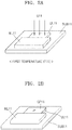
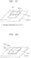
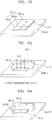
- FIGS. 1A through 1E are perspective views illustrating a method of forming a graphene layer, according to an exemplary embodiment.
- an underlayer UL10 may be formed on a substrate SUB10.
- the substrate SUB10 may be, for example, a silicon (Si) substrate.
- the substrate SUB10 may be a substrate other than a Si substrate.
- the underlayer UL10 may be a material layer including a catalyst for forming graphene on the underlayer UL10.
- the catalyst may be a metal.
- the underlayer UL10 may be referred to as a catalytic metal layer.
- the underlayer UL10 may include platinum (Pt) as the catalyst.
- the underlayer UL10 may be a Pt layer.
- the catalyst included in the underlayer UL10 is not limited to Pt and may be varied.
- the catalyst may include, for example, Ni, Cu, or Ir instead of Pt.
- a mask layer ML10 may be formed on the substrate SUB10 so as to cover a portion of the underlayer UL10.
- the mask layer ML10 may be formed from metal, a metal compound, oxide, nitride, or the like, and may also be formed from a polymer material that may be used at a high temperature (for example, at a temperature of about 500°C or more).
- An exposed region of the underlayer region UL10 that is not covered by the mask layer ML10 may be referred to as a first region.
- a process of forming graphene may be performed at a first temperature T10 by using a first source gas G10.
- the material of the first source gas G10 may be adsorbed onto the exposed region (i.e., the first region) of the underlayer UL10 by injecting the first source gas G10 into a chamber (not shown) containing the substrate SUB10, and the substrate SUB10 or the chamber may be heated at the first temperature T10.
- the heating process may be performed after injecting the first source gas G10 into the chamber, or the first source gas G10 may be injected into the chamber after the heating process has been completed. Alternatively, the heating process and the injection process may be performed at the same time.
- a first graphene GP10 may be formed on the first region of the underlayer UL10, as illustrated in FIG. 1C .
- the first graphene GP10 may be a first type of semiconductor layer.
- the first graphene GP10 may be a P-type graphene.
- the process of forming the first graphene GP10 may be a chemical vapor deposition (CVD) process. Forming the first graphene GP10 by using the source gas G10 and the first temperature T10 will be described later in detail.
- a region of the underlayer UL10 covered by the mask layer ML10 of FIG. 1C may be exposed by removing the mask layer ML10.
- the region of the underlayer UL10 exposed by removing the mask layer ML10 may be referred to as a second region.
- the second region of the underlayer UL10 may be adjacent to the first region.
- a process of forming graphene may be performed at a second temperature T20 by using a second source gas G20.
- the material of the second source gas G20 may be adsorbed onto the exposed region (i.e., the second region) of the underlayer UL10 by injecting the second source gas G20 into the chamber (not shown) containing the substrate SUB10, and the substrate SUB10 or the chamber may be heated at the second temperature T20.
- the heating process may be performed after injecting the second source gas G20 into the chamber, or the second source gas G20 may be injected into the chamber after the heating process has been completed. Alternatively, the heating process and the injection process may be performed at the same time.
- a second graphene GP20 may be formed on the second region of the underlayer UL10, as illustrated in FIG. 1E .
- the second graphene GP20 may be a second type of semiconductor.
- the second graphene GP20 may be an N-type graphene.
- the first graphene GP10 and the second graphene GP20 may be joined together.
- the second graphene GP20 may be joined to the side of the first graphene GP10. Accordingly, the first and second graphenes GP10 and GP20 may form a P-N junction.
- the combined first and second graphene GP10 and GP20 may be jointly referred to as a graphene layer GL10.
- the graphene layer GL10 may have a P-N junction.
- the first source gas G10 of FIG. 1B and the second source gas G20 of FIG. 1D may be the same as each other.
- the first source gas G10 and the second source gas G20 may each include a hydrocarbon compound containing nitrogen (N).
- the hydrocarbon compound containing nitrogen (N) may include, for example, pyridine (C 5 H 5 N). That is, both the first source gas G10 and the second source gas G20 may include a C 5 H 5 N gas.
- the first and second graphenes GP10 and GP20 having different semiconductor types may be formed by using different processing temperatures, i.e., the first and second temperatures T10 and T20.
- the first temperature T10 may be higher than the second temperature T20.
- the first temperature T10, which is used for forming the first graphene GP10 may be about 700°C or more
- the second temperature T20 which is used for forming the second graphene GP20, may be about 550°C or less. More specifically, the first temperature T10 may be from about 700°C to about 1200°C
- the second temperature T20 may be from about 450°C to about 550°C.
- the first graphene GP10 of FIG. 1C may not include nitrogen (N) atoms.
- Nitrogen (N) atoms may act as N-type dopants with respect to graphene.
- nitrogen (N) atoms may not be present in the first graphene GP10.
- the first graphene GP10 may be formed so as to be a P-type graphene as a result of doping effects caused by the underlayer UL10.
- the Dirac point of the first graphene GP10 may increase to hundreds of millivolts (for example, about 300 mV) above the Fermi level because of a component (e.g., Pt) of the underlayer UL10, and as a result, the first graphene GP10 may have P-type semiconductor properties.
- the nitrogen (N) in the C 5 H 5 N may remain. Accordingly, the nitrogen (N), in combination with carbon (C), may be used for forming graphene (the second graphene GP20 of FIG. 1E ).
- the second graphene GP20 of FIG. 1E may include nitrogen (N) atoms. Since the nitrogen (N) atoms may be N-type dopants, the second graphene GP20 may have N-type properties due to the nitrogen (N) atoms.
- the number of nitrogen (N) atoms included in the second graphene GP20 varies according to changes in the second temperature T20, and as a result, the doping concentration of the second graphene GP20 may vary depending on the second temperature T20.
- the second temperature T20 is relatively low (for example, about 450°C)
- the N-doping concentration in the second graphene GP20 may increase.
- the second temperature T20 is relatively high (for example, about 550°C)
- the doping concentration of the second graphene GP20 may be easily controlled by adjusting the second temperature T20 within a predetermined range.
- a P-type graphene (i.e., the first graphene GP10) and an N-type graphene (i.e., the second graphene GP20) may be formed by using one type of source gas while varying the process temperature used in a graphene formation process. Since only one type of source gas is used, processes to produce graphene may be simplified, manufacturing costs may be reduced, and manufacturing time may be reduced.
- a junction i.e., P-N junction formed between the P-type graphene (i.e., the first graphene GP10) and the N-type graphene (i.e., the second graphene GP20) formed by the method described above may have excellent characteristics.
- the P-type and N-type graphenes i.e., the first and second graphenes GP10 and GP20
- the graphene layer GL10 formed from the P-type and N-type graphenes may have excellent characteristics and properties.
- the crystalline structure and characteristics of the graphene layer GL10 will be described later in more detail with reference to FIG. 9 .
- the second graphene GP20 When forming the second graphene GP20 by using the second source gas G20 and the second temperature T20 after the first graphene GP10 is formed, carbon (C) atoms reach a stable state in terms of potential energy.
- the second graphene GP20 may be formed adjacent to the first graphene GP10. Accordingly, the boundary between the first graphene GP10 and the second graphene GP20 may not have defects or may have few defects. That is, the bond between the first graphene GP10 and the second graphene GP20 may be practically a chemical bond.
- first graphene GP10 and the second graphene GP20 may be formed only on the surface of the underlayer UL10, the first graphene GP10 and the second graphene GP20 may each have a single atomic layer structure or a structure similar thereto.
- FIGS. 1A through 1E a method of forming the P-type and N-type graphenes GP10 and GP20 by using the same source gas for both the first source gas G10 and the second source gas G20 has been described.
- P-type and N-type graphenes may be formed by using different source gases.
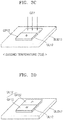
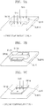
- FIGS. 2A through 2D are perspective views illustrating a method of forming a graphene layer, according to another exemplary embodiment.
- a mask layer ML11 covering a portion of an underlayer UL11 may be formed after forming the underlayer UL11 on a substrate SUB11.
- This structure may be similar to the structure of FIG. 1B in which the underlayer UL10 and the mask layer ML10 are formed on the substrate SUB10.
- the underlayer UL11 may include a catalyst, such as Pt, Ni, Cu, or Ir, and the mask layer ML11 may be formed from metal, a metal compound, oxide, nitride, or polymer.
- a process of forming graphene may be performed at a first temperature T11 by using a first source gas G11.
- a first graphene GP11 may be formed on a region (a first region) of the underlayer UL11, not covered by the mask layer ML11, as illustrated in FIG. 2B .
- the first graphene GP11 may be, for example, a P-type graphene.
- a process of forming graphene may be performed at a second temperature T21 by using a second source gas G21 after removing the mask layer ML11.
- a second graphene GP21 joined to the first graphene GP11 may be formed as illustrated in FIG. 2D .
- the second graphene GP21 may be, for example, an N-type graphene.
- the combined first and second graphenes GP11 and GP21 may be jointly referred to as graphene layer GL11.
- the first source gas G11 of FIG. 2A and the second source gas G21 of FIG. 2C may be different from each other.
- the first source gas G11 may include a first hydrocarbon compound and the second source gas G21 may include a second hydrocarbon compound.
- the first hydrocarbon compound may not contain nitrogen (N), and the second hydrocarbon compound may contain N.
- the first source gas G11 may include a hydrocarbon compound, such as benzene (C 6 H 6 ), ethylene (C 2 H 4 ), or acetylene (C 2 H 2 ).
- C 6 H 6 , C 2 H 4 , and C 2 H 2 are compounds formed of only carbon (C) and hydrogen (H).
- the first source gas G11 may also include a hydrocarbon compound containing boron (B), for example, triethylborane (C 6 H 15 B). Accordingly, the first source gas G11 may include at least one of C 6 H 6 , C 2 H 4 , C 2 H 2 , and C 6 H 15 B.
- the second source gas G21 may include a hydrocarbon compound containing nitrogen (N), for example, C 5 H 5 N.
- N nitrogen
- the first temperature T11 and the second temperature T21 may be different from each other or the same as each other.
- the first temperature T11 may be higher than the second temperature T21 or vice versa. In some cases, the first temperature T11 and the second temperature T21 may be the same as or similar to each other.
- the first temperature T11 when the first source gas G11 includes C 6 H 6 , C 2 H 4 , or C 2 H 2 , the first temperature T11 may be from about 450°C to about 1200°C.
- the first temperature T11 when the first source gas G11 includes C 6 H 15 B, the first temperature T11 may be from about 320°C to about 630°C.
- the first graphene GP11 of FIG. 2B may be formed so as to be a P-type graphene. Accordingly, the first temperature T11 may be within the range of from about 320°C to about 1200°C.
- the first graphene GP11 may be formed from only carbon (C) atoms and may have P-type semiconductor characteristics as a result of the underlayer UL11.
- the first gas G11 is a hydrocarbon compound containing boron (B), such as C 6 H 15 B
- the first graphene GP11 may be formed so as to include boron (B) atoms and may have P-type semiconductor characteristics as a result of the boron (B) atoms.
- the boron (B) atoms may act as P-type dopants with respect to the graphene.
- the second temperature T21 when the second source gas G21 includes C 5 H 5 N, the second temperature T21 may be about 550°C or less.
- the formed graphene i.e., the second graphene GP21 of FIG. 2D
- the second graphene GP21 may be the same as the second graphene GP20 described with reference to FIGS. 1D and 1E .
- the range of the second temperature T21 may be from about 450°C to about 550°C.
- the first graphene GP11 may be a P-type graphene and the second graphene GP21 may be an N-type graphene, as described above.
- a P-type graphene may be formed after forming an N-type graphene.
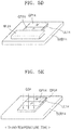
- FIGS. 3A through 3D are perspective views illustrating a method of forming a graphene layer, according to another exemplary embodiment.
- an underlayer UL12 may be formed on a substrate SUB12 and a mask layer ML12 may be formed to cover a portion of the underlayer UL12.
- the material of the substrate SUB12, the material of the underlayer UL12, and the material of the mask layer ML12 may be the same as or similar to the material of the substrate SUB11, the material of the underlayer UL11, and the material of the mask layer ML11, respectively.
- a process of forming graphene may be performed at a first temperature T12 by using a first source gas G12.
- a first graphene GP12 may be formed on a region (a first region) of the underlayer UL12, not covered with the mask layer ML12, as illustrated in FIG. 3B .
- the first graphene GP12 may be, for example, an N-type graphene.
- a process of forming graphene may be performed at a second temperature T22 by using a second source gas G22 after removing the mask layer ML12.
- a second graphene GP22 joined to the first graphene GP12 may be formed as illustrated in FIG. 3D .
- the second graphene GP22 may be, for example, a P-type graphene.
- the combined first and second graphenes GP12 and GP22 may be jointly referred to as a graphene layer GL12.
- the first source gas G12 of FIG. 3A and the second source gas G22 of FIG. 3C may be different from each other.
- the first source gas G12 may be the same as or similar to the second source gas G21 of FIG. 2C
- the second source gas G22 may be the same as or similar to the first source gas G11 of FIG. 2A .
- the first source gas G12 may include a second hydrocarbon compound and the second source gas G22 may include a first hydrocarbon compound as previously described.
- the second hydrocarbon compound may contain nitrogen (N), and the first hydrocarbon compound may not contain nitrogen (N).
- the first source gas G12 may include a hydrocarbon compound containing nitrogen (N), for example, C 5 H 5 N.
- the second source gas G22 may include a hydrocarbon compound containing boron (B), for example, C 6 H 15 B or may include a hydrocarbon compound, such as C 6 H 6 , C 2 H 4 , or C 2 H 2 .
- B hydrocarbon compound containing boron
- the second temperature T22 that is used for forming the second graphene GP22 may be lower than or the same as the first temperature T12 that is used for forming the first graphene GP12, in order to reduce damage to the first graphene GP12 during the formation of the second graphene GP22.
- the formed graphene i.e., the first graphene GP12 of FIG. 3B
- the first temperature T12 may be from about 450°C to about 550°C.
- the second temperature T22 may be controlled so as to be lower than about 550°C or to be lower than about 500°C.
- the P-type graphene i.e., the second graphene GP22
- the P-type graphene may be formed at a temperature of around 450°C, around 500°C, or around 530°C.
- the second temperature T22 When the second temperature T22 is too high, nitrogen (N) atoms in the first graphene GP12 may decompose, and thus the first graphene GP12 may be damaged. Accordingly, the second temperature T22 may be appropriately controlled so as to prevent damage to the first graphene GP12.
- FIGS. 4A through 4F are perspective views illustrating a method of forming a graphene layer, according to another exemplary embodiment.
- a mask layer ML13 covering a portion of an underlayer UL13 may be formed after forming the underlayer UL13 on a substrate SUB13.
- a process of forming graphene may be performed at a first temperature T13 by using a first source gas G13.
- the first source gas G13 and the first temperature T13 may correspond to the first source gas G10 and the first temperature T10 of FIG. 1B or correspond to the first source gas G11 and the first temperature T11 of FIG. 2A .
- a first graphene GP13 may be formed as illustrated in FIG. 4B .
- the first graphene GP13 may be, for example, a P-type graphene.
- a second mask layer ML23 may be formed after removing the first mask layer ML13. A portion of the underlayer UL13 may be exposed without being covered with the second mask layer ML23.
- a process of forming graphene may be performed at a second temperature T23 by using a second source gas G23.
- the second source gas G23 and the second temperature T23 may correspond to the second source gas G20 and the second temperature T20 of FIG. 1D or may correspond to the second source gas G21 and the second temperature T21 of FIG. 2C .
- a second graphene GP23 may be formed as illustrated in FIG. 4D .
- the second graphene GP23 may be, for example, an N-type graphene.
- a process of forming graphene may be performed on an exposed region of the underlayer UL13 after removing the second mask layer ML23.
- a third source gas G33 and a third temperature T33 may be used.
- the third source gas G33 and the third temperature T33 may correspond to the second source gas G22 and the second temperature T22 of FIG. 3C .
- the third source gas G33 may include a hydrocarbon compound containing boron (B), for example, C 6 H 15 B or may include a hydrocarbon compound, such as C 6 H 6 , C 2 H 4 , or C 2 H 2 .
- the third temperature T33 may be a temperature of about 550°C or less or about 500°C or less.
- the third temperature may be lower than either the first or the second temperature.
- a third graphene GP33 may be formed as illustrated in FIG. 4F .
- the third graphene GP33 may be, for example, a P-type graphene.
- the third graphene GP33 may be the same as or similar to the second graphene GP22 of FIG. 3D .
- the first through third graphenes GP13, GP23, and GP33 may jointly form a graphene layer GL13.
- the graphene layer GL13 may have a PNP junction structure.
- the sizes and forms of the first through third graphenes GP13, GP23, and GP33 may be variously changed.
- a graphene layer having an NPN junction structure may be formed by modifying the example, as illustrated in FIGS. 5A through 5F .
- a graphene layer GL14 including first through third graphenes GP14, GP24, and GP34 may be formed on an underlayer UL14 on a substrate SUB14.
- the first graphene GP14 may be an N-type graphene
- the second graphene GP24 may be a P-type graphene
- the third graphene GP34 may be an N-type graphene. Accordingly, the graphene layer GL14 may have an NPN junction structure.
- reference numeral ML14 denotes a first mask layer
- reference numeral G14 denotes a first source gas
- reference numeral T14 denotes a first temperature
- reference numeral ML24 denotes a second mask layer
- reference numeral G24 denotes a second source gas
- reference numeral T24 denotes a second temperature
- reference numeral G34 denotes a third source gas
- reference numeral T34 denotes a third temperature.
- the first source gas G14 and the first temperature T14 of FIG. 5A may correspond to the first source gas G12 and the first temperature T12 of FIG. 3A .
- the third source gas G34 and the third temperature T34 of FIG. 5E may correspond to the second source gas G20 and the second temperature T20 of FIG. 1D , may correspond to the second source gas G21 and the second temperature T21 of FIG. 2C , or may correspond to the first source gas G14 and the first temperature T14 of FIG. 5A .
- FIGS. 4A through 4F and the method shown in FIGS. 5A through 5F may be variously modified. Modified examples are illustrated in FIGS. 6A through 6D and FIGS. 7A through 7D .
- FIGS. 6A through 6D are perspective views illustrating a method of forming a graphene layer, according to another exemplary embodiment.
- FIGS. 7A through 7D are perspective views illustrating a method of forming a graphene layer, according to another exemplary embodiment.
- a mask layer ML15 covering a portion of an underlayer UL15 may be formed after forming the underlayer UL15 on a substrate SUB15.
- a region of the underlayer UL15 may be exposed at both sides of the mask layer ML15.
- a process of forming graphene may be performed on the exposed region of the underlayer UL15.
- a first source gas G15 and a first temperature T15 may be used.
- the first source gas G15 and the first temperature T15 may correspond to the first source gas G10 and the first temperature T10 of FIG. 1B or may correspond to the first source gas G11 and the first temperature T11 of FIG. 2A .
- a first graphene GP15 and a third graphene GP35 may be formed as illustrated in FIG. 6B .
- the first graphene GP15 and the third graphene GP35 may be, for example, P-type graphenes.
- a process of forming graphene may be performed on an exposed region of the underlayer UL15 after removing the mask layer ML15.
- a second source gas G25 and a second temperature T25 may be used.
- the second source gas G25 and the second temperature T25 may correspond to the second source gas G20 and the second temperature T20 of FIG. 1D or may correspond to the second source gas G21 and the second temperature T21 of FIG. 2C .
- a second graphene GP25 may be formed as illustrated in FIG. 6D .
- the second graphene GP25 may be disposed between the first graphene GP15 and the third graphene GP35.
- the second graphene GP25 may be, for example, an N-type graphene. Accordingly, a graphene layer GL15 including the first through third graphenes GP15, GP25, and GP35 may have a PNP junction structure.
- FIGS. 6A through 6D may be modified as shown in FIGS. 7A through 7D .
- a graphene layer having an NPN structure may be formed by using a method as illustrated in FIGS. 7A through 7D .
- a graphene layer GL16 including first through third graphenes GP16, GP26, and GP36 may be formed on an underlayer UL16 on a substrate SUB16.
- the first graphene GP16 may be an N-type graphene
- the second graphene GP26 may be a P-type graphene
- the third graphene GP36 may be an N-type graphene. Accordingly, the graphene layer GL16 may have an NPN junction structure.
- reference numeral ML16 denotes a mask layer
- reference numeral G16 denotes a first source gas
- reference numeral T16 denotes a first temperature
- reference numeral G26 denotes a second source gas
- reference numeral T26 denotes a second temperature.
- the first source gas G16 and the first temperature T16 of FIG. 7A may correspond to the first source gas G12 and the first temperature T12 of FIG. 3A
- the second source gas G26 and the second temperature T26 of FIG. 7C may correspond to the second source gas G22 and the second temperature T22 of FIG. 3C .
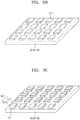
- FIGS. 8A through 8C are perspective views illustrating a method of forming a graphene layer, according to another exemplary embodiment.
- an under-material layer UL100 may be formed on a substrate SUB100.
- the substrate SUB100 may be formed of a material that is the same as or similar to those of the substrates SUB10 to SUB16 of FIGS. 1 through 7 .
- the under-material layer UL100 may be formed from a material that is the same as or similar to those of underlayers UL10 to UL16 in FIGS. 1 through 7 .
- the under-material layer UL100 may be a catalytic material layer that is a metal layer.
- a plurality of underlayers UL1 that are separate from one another may be formed by patterning the under-material layer UL100.
- Each of the plurality of underlayers UL1 may be the same as or similar to the underlayers UL10 to UL16 of FIGS. 1 through 7 .
- a graphene layer GL1 may be formed on each of the plurality of underlayers UL1.
- the graphene layer GL1 may include a first graphene GL1 and a second graphene GP2.
- the first graphene GP1 and the second graphene GP2 may be joined to each other.
- One of the first and second graphenes GP1 and GP2 may be a P-type graphene, and the other one of the first and second graphenes GP1 and GP2 may be an N-type graphene. Accordingly, the graphene layer GL1 may have a P-N junction structure.
- a method of forming the graphene layer GL1 may be that same as or similar to the method of forming the graphene layer GL10 of FIG. 1E , the method of forming the graphene layer GL11 of FIG. 2D , or the method of forming the graphene layer GL12 of FIG. 3D .
- the graphene layer GL1 has a P-N structure
- the graphene layer GL1 may have a PNP structure or an NPN structure.
- a method of forming the graphene layer GL1 may be the same as or similar to those described with reference to FIGS. 4A through 7D .
- one graphene sheet is formed (or transferred) onto a substrate and then a plurality of graphene layers, which are separate from one another, are formed by patterning (etching) the graphene sheet, the edge portions of each graphene layer may be damaged as a result of the etching.
- a portion of the photoresist (PR) used in the patterning (etching) may remain on the plurality of graphene layers, and thus, the physical properties of the plurality of graphene layers and the characteristics of a device including the plurality of graphene layers may be degraded.
- PR photoresist
- the graphene layer GL1 is formed on each of the plurality of underlayers UL1 patterned in advance, and thus, the edge portions of the graphene layer GL1 may be prevented from being damaged and the PR may be prevented from remaining.
- etching (patterning) for the under-material layer UL100 may be easier than directly etching (patterning) a graphene sheet, the size and shape of the graphene layer GL1 may be easily controlled by forming a patterned graphene layer GL1 on a patterned under-material layer UL100 after pattering (etching) the under-material layer UL100.
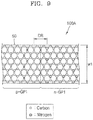
- FIG. 9 is a plan view illustrating a structure of a graphene layer according to an exemplary embodiment.
- the graphene layer 100A may be disposed on an underlayer 50.
- the graphene layer 100A may include a P-type graphene p-GP1 and an N-type graphene n-GP1.
- the N-type graphene n-GP1 may be joined to the side of the P-type graphene p-GP1.
- the N-type graphene n-GP1 may have a hexagonal crystalline structure formed from carbon (C) atoms, in which some carbon (C) atoms are substituted with first atoms.
- the first atoms may be, for example, nitrogen (N) atoms.
- the nitrogen (N) atoms may act as N-type dopants.
- nitrogen (N) atoms form a hexagonal crystalline structure along with carbon (C) atoms
- other atoms may be used instead of the nitrogen (N) atoms.
- the P-type graphene p-GP1 may have a hexagonal crystalline structure formed from only carbon (C) atoms.
- the P-type graphene p-GP1 may have P-type semiconductor characteristics due to doping effects by an underlayer 50 disposed under the P-type graphene p-GP1.
- the underlayer 50 may include a catalytic metal, such as Pt.
- the material of the underlayer 50 is not limited to Pt and may be changed in various manners.
- a depletion region DR formed at the interface between the P-type graphene p-GP1 and the N-type n-GP1 may have, for example, a width of about 5 nm or less.
- the width of the depletion region DR may be about 2 nm or less.
- the width of the depletion region DR may be around 1 nm.
- the N-type graphene n-GP1 may have N-type semiconductor characteristics since carbon (C) atoms are substituted with the first atoms (e.g., nitrogen (N) atoms).
- the first atoms e.g., nitrogen (N) atoms
- the P-type graphene p-GP1 may have P-type semiconductor characteristics due to a change (rise) of the Dirac point by the underlayer 50.
- the junction between the P-type graphene p-GP1 and the N-type graphene n-GP1 may have an atomic-scale size (width), and a depletion region DR having a very small width may be formed between the P-type graphene p-GP1 and the N-type graphene n-GP1.
- the depletion region DR may have a width in a range of from about 5 nm or less or about 2 nm or less.
- the N-doping effects caused by the nitrogen (N) atoms may disappear in a region that is at a distance greater than about 2 nm from a position where nitrogen (N) atoms exist.
- the width of the depletion region DR may be about 2 nm or less.
- a boundary between the P-type graphene p-GP1 and the N-type graphene n-GP1, formed by the method described above, may not have defects or may have few defects.
- the graphene layer 100A may have excellent physical properties and characteristics.
- the boundary between the P-type doping region and the N-type doping region may have a width of tens of micrometers ( ⁇ m) or more, for example, a width of about 100 ⁇ m. Accordingly, it is difficult to implement excellent P-N junction characteristics and it is difficult to manufacture a graphene device having a small size (width) of 100 ⁇ m or less. Such an issue may also occur identically (or similarly) in the case of depositing a metal oxide on a portion of a graphene sheet to form a P-N junction.
- the boundary (depletion region) between the P-type graphene p-GP1 and the N-type graphene n-GP1 may be formed on a very small scale within several nanometers (nm), and thus, excellent P-N junction characteristics may be obtained and a graphene device having a small size may be easily manufactured.
- the uniformity of doping concentration may be improved in each of the N-type and P-type graphenes n-GP1 and p-GP1.
- the deviation in doping concentration by region may be smaller than about 2.5 ⁇ 10 12 /cm 2 .
- the difference between the doping concentration of a first region having a maximum doping concentration and the doping concentration of a second region having a minimum doping concentration may be smaller than about 2.5 ⁇ 10 12 /cm 2 .
- nitrogen (N) atoms may be uniformly or almost uniformly distributed in the entire graphene (N-type graphene) since the nitrogen (N) atoms are used in the process of depositing the graphene (N-type graphene). Accordingly, uniformity in the doping concentration may be easily secured.
- the doping concentration of graphene may be easily controlled by adjusting the heating temperature or the concentration of the source gas when forming the graphene (N-type graphene).
- N-type graphene N-type graphene
- the entire edge portion of the graphene layer 100A may have a defect-free crystalline structure.
- the entire edge portion of the graphene layer 100A may have a defect-free zigzag structure. Since the graphene layer 100A is formed on the underlayer 50 without directly patterning (etching) the graphene sheet, the edge portion of the graphene layer 100A may be undamaged and may have a defect-free crystalline structure. Accordingly, the graphene layer 100A may have excellent characteristics and a graphene device using the graphene layer 100A may exhibit excellent performance.
- the width w1 of the graphene layer 100A may be several nm to several hundred nm.
- the width w1 is a width in a short length direction of the graphene layer 100A.
- the width w1 of the graphene layer 100A may be, for example, about 500 nm or less or about 100 nm or less.
- the graphene layer 100A may be formed so as to have a faultless edge portion while having a small width w1 of about 500 nm or less or about 100 nm or less.
- a graphene layer having a small width of about 1 ⁇ m or less it may be difficult to form a graphene layer having a small width of about 1 ⁇ m or less by using an existing method, for example, the method of directly etching (patterning) a graphene sheet.
- an existing method for example, the method of directly etching (patterning) a graphene sheet.
- characteristics of the graphene layer may be degraded as a result of defects in an edge portion.
- photoresist PR used during the etching (patterning) may remain on the graphene layer, thereby degrading the characteristics of the graphene layer. According to the current exemplary embodiment, on the other hand, such problems may be prevented and solved, and a graphene layer having excellent characteristics may therefore be easily formed.
- the size and shape of each of the plurality of graphene layers may be easily controlled and, in addition, the interval between two adjacent graphene layers may be easily controlled within several tens of nm or to the extent of several nm. Accordingly, the methods and the structures according to the exemplary embodiments described above may be usefully applied to a device (for example, a device of FIG. 17C to be described later) using two adjacent graphene layers.
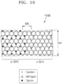
- FIG. 10 is a plan view illustrating a structure of a graphene layer according to another exemplary embodiment.
- the graphene layer 100B may include a P-type graphene p-GP2 and an N-type graphene n-GP2.
- the n-type graphene n-GP2 may have substantially the same crystalline structure as the n-type graphene n-GP1 of FIG. 9 .
- the N-type graphene n-GP2 may have a hexagonal crystalline structure formed from carbon (C) atoms, in which some carbon (C) atoms are substituted with first atoms.
- the first atoms may be, for example, nitrogen (N) atoms.
- the P-type graphene p-GP2 may have a hexagonal crystalline structure formed from carbon (C) atoms, in which some carbon (C) atoms are substituted with second atoms that are different from the first atoms.
- the second atoms may be, for example, boron (B) atoms.
- the boron (B) atoms may act as P-type dopants.
- an underlayer may be further disposed under the P-type and N-type graphenes p-GP2 and n-GP2.
- the underlayer may include a catalytic metal. Examples of the catalytic metal may include Pt, Cu, Ni, Ir, and the like.
- a depletion region DR having a very small width may be formed in an interfacial portion between the P-type graphene p-GP2 and the N-type graphene n-GP2.
- the width of the depletion region DR may be from about 5 nm or less or about 2 nm or less.
- Each of the P-type and N-type graphenes p-GP2 and n-GP2 may have excellent doping uniformity.
- the deviation in doping concentration by region may be smaller than about 2.5 ⁇ 10 12 /cm 2 .
- the entire edge portion of the graphene layer 100B may have a defect-free crystalline structure, for example, a defect-free zigzag structure.
- the width w1 of the graphene layer 100B is a width in a short length direction and may be several nm to several hundred of nm, for example, about 500 nm or less or about 100 nm or less.
- the structure of the graphene layer 100A illustrated in FIG. 9 or the structure of the graphene layer 100B illustrated in FIG. 10 may correspond to that of any one of the graphene layers GL10 to GL16 and GL1 illustrated in FIGS. 1 through 8 .
- at least a portion of any one of the graphene layers GL10 to GL16 and GL1 illustrated in FIGS. 1 through 8 may have the structure of the graphene layer 100A illustrated in FIG. 9 or the structure of the graphene layer 100B illustrated in FIG. 10 .
- the first graphene GP11 and the second graphene GP21 of FIG. 2D may correspond to the P-type graphene p-GP1 and the N-type graphene n-GP1 of FIG. 9 , respectively, or may correspond to the P-type graphene p-GP2 and the N-type graphene n-GP2 of FIG. 10 , respectively.
- the size of honeycomb unit structures forming the hexagonal crystalline structures of the graphene layers 100A and 100B is arbitrarily determined for convenience's sake.
- the ratio of the actual length of the depletion region DR to the actual size of the honeycomb unit structures may be different from that illustrated in FIGS. 9 and 10 .
- the length of the depletion region DR has a length equal to the combined length of two honeycomb unit structures, the actual length of the depletion region DR may be different therefrom.
- the ratio between the size of the honeycomb unit structures and the width w1 of the graphene layers 100A and 100B in FIGS. 9 and 10 may be different from that of an actual embodiment.
- FIG. 11 illustrates X-ray photoelectron spectroscopy (XPS) images for a graphene layer having a P-N junction, formed by a method according to a comparative example.
- XPS X-ray photoelectron spectroscopy
- FIG. 11 illustrates images captured in different ways with respect to the same graphene layer.
- View (A) of FIG. 11 illustrates an image captured so that a region including an N-type doping material is brightly seen
- view (B) of FIG. 11 illustrates an image captured so that a region including a P-type doping material is brightly seen.
- the graphene layer according to the comparative example is formed by forming a pattern layer of 3-aminopropyltriethoxysilane (APTES) and a pattern of perfluorooctyltriethoxy silane (PFES) via lithography, transferring a graphene sheet onto the patterns, and then annealing. In the annealing process, P-type and N-type doping regions may be formed in a graphene sheet by the APTES and the PFES.
- APTES 3-aminopropyltriethoxysilane
- PFES perfluorooctyltriethoxy silane
- the boundary between the N-type doping region and the P-type doping region is not sharp. That is, the overlapping portion between the N-type doping region and the P-type doping region is considerably wide.
- the width of the overlapping portion between the N-type doping region and the P-type doping region is about 100 ⁇ m. This means that in the graphene layer formed by the method according to the comparative example, the depletion region between the N-type doping region and the P-type doping region is very wide. It may be difficult to manufacture a graphene device having a width of about 100 ⁇ m or less by using the method according to the comparison example.
- FIG. 12 is a diagram illustrating a graphene layer GL1 according to an exemplary embodiment and the structure of an edge portion thereof.
- FIG. 12 includes a scanning tunneling microscopy (STM) image captured with respect to the edge portion of the graphene layer.
- STM scanning tunneling microscopy
- the edge portion of the graphene layer GL1 has a defect-free zigzag structure.
- the edge portion may have a uniform crystalline structure.
- a plurality of patterned underlayers (catalytic metal layers) UL1 on a substrate SUB100, and the graphene layer GL1 may be formed on each patterned underlayer UL1.
- the graphene layer GL1 may include a first graphene GP1 and a second graphene GP2, and one of the first and second graphenes GP1 and GP2 may be a P-type graphene and the other one of the first and second graphenes GP1 and GP2 may be an N-type graphene.
- the graphene layer GL1 may be the same as that described with reference to FIG. 8C .
- FIG. 13 is a diagram illustrating the structure of an edge portion of a graphene layer according to a comparative example.
- a graphene layer is formed via a method of directly patterning (etching) a graphene sheet
- many defects may occur in the edge portion of the graphene layer.
- the crystalline structure of the edge portion may be non-uniform. Accordingly, the electrical characteristics of the graphene layer formed via such a method may be degraded.
- a portion of a PR used for the patterning (etching) may remain on the graphene layer, and thus, characteristics of the graphene layer may be deteriorated.
- a method of manufacturing a device i.e., a graphene-containing device including a graphene layer, according to an exemplary embodiment is described below.
- FIGS. 14A through 14C are perspective views illustrating a method of manufacturing a graphene-containing device, according to an exemplary embodiment.
- a graphene layer GL110 having a P-N junction structure may be formed on an underlayer UL110 after the underlayer UL110 is formed on a first substrate SUB110.
- the graphene layer GL110 may include a first graphene GP110 and a second graphene GP210.
- the first graphene GP110 may be a P-type graphene
- the second graphene GP210 may be an N-type graphene.
- the method of forming the graphene layer GL110 on the first substrate SUB110 may be the same as or similar to that described with reference to FIGS. 1 through 8 .
- the graphene layer GL110 on the first substrate SUB110 may be transferred to a second substrate SUB210.
- the method of transferring the graphene layer GL110 from the first substrate SUB110 to the second substrate SUB210 may be a generally-known graphene transfer method.
- the second substrate SUB210 may be a semiconductor substrate or an insulating substrate.
- the semiconductor substrate may be, for example, a silicon substrate.
- the graphene layer GL110 may be transferred onto an insulating layer after the insulating layer is formed on the semiconductor substrate.
- a conductive substrate may also be used as the second substrate SUB210. In this case, the graphene layer GL110 may be transferred onto an insulating layer after the insulating layer is formed on the conductive substrate.
- a device portion including the graphene layer GL110 may be formed on the second substrate SUB210.
- a first electrode E110 electrically connected to and contacting the first graphene GP110 may be formed on the second substrate SUB210
- a second electrode E210 electrically connected to and contacting the second graphene GP210 may be formed on the second substrate SUB210. Since the graphene layer GL110 has a P-N junction structure, the graphene layer GL110 and the first and second electrodes E110 and E210 being in contact with the graphene layer GL110 may form a diode device.
- FIGS. 15A through 15C are cross-sectional views illustrating a method of manufacturing a graphene-containing device, according to another exemplary embodiment.
- an underlayer UL120 and a graphene layer GL120 may be sequentially formed on a first substrate SUB120.
- the method of sequentially forming the underlayer UL120 and the graphene layer GL120 on the first substrate SUB120 may be the same as or similar to that described with reference to FIGS. 1 through 8 .
- the graphene layer GL120 on the first substrate SUB120 may be transferred onto a second substrate SUB220.
- the method of transferring the graphene layer GL120 onto the second substrate SUB220 may be the same as or similar to the transfer method described with reference to FIG. 14B .
- the material of the second substrate SUB220 may also be the same as or similar to that of the second substrate SUB210 of FIG. 14B .
- a device portion including the graphene layer GL120 may be formed on the second substrate SUB220.
- a source electrode S120 and a drain electrode D120 which contact both ends of the graphene layer GL120, may be formed.
- a gate insulating layer GI120 may be formed to cover the source electrode S120, the drain electrode D120, and the graphene layer GL120 between the source electrode S120 and the drain electrode D120, and a gate electrode G120 may be formed on the gate insulating layer GI120.
- the gate electrode G120 may be disposed on the graphene layer GL120.
- the device portion of FIG. 15C may be a transistor, and the graphene layer GL120 may be used as a channel layer in the transistor.
- the graphene layer GL120 may have a PNP structure or an NPN structure.
- the source electrode S120 and the drain electrode D120 may respectively contact different P-type regions of the graphene layer GL120.
- the source electrode S120 and the drain electrode D120 may respectively contact different N-type regions of the graphene layer GL120.
- the transistor of FIG. 15C may have a top-gate structure in which the gate electrode G120 is disposed on the graphene layer GL120, which may be used as a channel layer in the transistor.
- FIGS. 16A through 16C are cross-sectional views illustrating a method of manufacturing a graphene-containing device, according to another exemplary embodiment.
- an underlayer UL130 and a graphene layer GL130 may be sequentially formed on a first substrate SUB130.
- This structure may be the same as or similar to the structure of FIG. 15A .
- the graphene layer GL130 on the first substrate SUB130 may be transferred onto a second substrate SUB230.
- the graphene layer GL130 may be transferred onto the gate insulating layer GI130.
- the method of transferring the graphene layer GL130 may be the same as or similar to the transfer method described with reference to FIG. 14B .
- a source electrode S130 and a drain electrode D130 which contact both ends of the graphene layer GL130, may be formed on the gate insulating layer GI130.
- the device of FIG. 16C may be a transistor having a bottom-gate structure, and the graphene layer GL130 may be used as a channel layer.
- the graphene layer GL130 may have a PNP junction structure or an NPN junction structure.
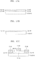
- FIGS. 17A through 17C are cross-sectional views illustrating a method of manufacturing a graphene-containing device, according to another exemplary embodiment.
- a plurality of underlayers UL140 may be formed on a first substrate SUB140 and a plurality of graphene layers GL140 may be formed on the plurality of underlayers UL140.
- the structure of FIG. 17A may be formed by using a method that is the same as or a similar to that described with reference to FIGS. 8A through 8C .
- the plurality of graphene layers GL140 on the first substrate SUB140 may be transferred onto a second substrate SUB240.
- a method of transferring the plurality of graphene layers GL140 may be the same as or similar to the transfer method described with reference to FIG. 14B .
- a device portion including the plurality of graphene layers GL140 may be formed on the second substrate SUB240.
- a gate insulating layer GI140 may be formed on a tunneling layer TL140 and the plurality of graphene layers GL140 after the tunneling layer TL140, filling a region between the plurality of graphene layers, GL140 is formed.
- a gate electrode G140 may be formed on the gate insulating layer GI140, and a source electrode S140 and a drain electrode D140, electrically connected to and contacting the graphene layers GL140, may be formed.
- the width of the tunneling layer TL140 and the material used to form the tunneling layer TL140 may be chosen such that Fowler-Nordheim tunneling of electric charges may occur therein.
- the width of the tunneling layer TL140 may be from about several nm to about several tens of nm.
- the device portion of FIG. 17C may be a field effect transistor (FET) using a tunneling effect.
- FET field effect transistor
- the device portion of FIG. 17C may be referred to as a kind of tunneling device.
- the interval between two graphene layers GL140 may be easily controlled within about several tens of nm or to the extent of about several nm, and thus, a device having a structure as shown in FIG. 17C may be easily manufactured.
- edge portions of the two graphene layers GL140 grown on the underlayers UL140 may have defect-free crystalline structures, and thus the performance of the device may be improved.
- FIGS. 14A through 17C a graphene-containing device is manufactured on a second substrate after transferring a graphene layer from a first substrate to the second substrate
- the graphene-containing device may be manufactured on the first substrate without performing the step of transferring.
- An example of this case is illustrated in FIGS. 18A and 18B .
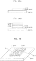
- FIGS. 18A and 18B are cross-sectional views illustrating a method of manufacturing a graphene-containing device, according to another exemplary embodiment.
- an underlayer UL150 and a graphene layer GL150 may be sequentially formed on a first substrate SUB150.
- the structure of FIG. 18A may be the same as or similar to that of FIG. 15A .
- the underlayer UL150 may be a conductive layer, for example, a metal layer, and the graphene layer GL150 may be a semiconductor layer including a P-N junction.
- the underlayer UL150 is referred to as a first conductive layer CL150.
- a device portion including the graphene layer GL150 may be formed on the first substrate SUB150.
- a second conductive layer CL250, an insulating layer NL150, and a third conductive layer CL350 may be sequentially formed on the graphene layer GL150.
- the device portion of FIG. 18B may be a tunneling device.
- the graphene layer GL150 may be a tunneling layer.
- the first conductive layer CL150 may be a drain electrode
- the second conductive layer CL250 may be a source electrode
- the third electrode CL150 may be a gate electrode.
- the insulating layer NL150 may be a gate insulating layer. Electrical characteristics of the graphene layer GL150 or the characteristics of an interface between the second conductive layer CL250 and the graphene layer GL150 may be controlled by the third conductive layer CL350. Current may flow between the first conductive layer CL150 and the second conductive layer CL250 by the tunneling of electric charges through the graphene layer GL150.
- a graphene layer according to an exemplary embodiment may be applied to various devices (e.g., semiconductor devices and electronic devices) for various purposes.
- a graphene layer according to an exemplary embodiment may be applied to various devices, such as diodes, transistors, tunneling devices, memory devices, solar cells, photodetectors, sensors, light-emitting devices, logic devices, energy storage devices, and display devices.
- the transistors may have various structures, such as a field effect transistor (FET) structure, a thin film transistor (TFT) structure, a binary junction transistor (BJT) structure, and a barrier transistor (barristor) structure.
- the sensors may be optical sensors or gas sensors or may be sensors using graphene arrays.
- the graphene layer may be applied to every device using a P-N junction, may be used instead of silicon (Si) in a device using Si, and may be applied to stackable devices, flexible devices, and transparent devices. Since the graphene layer may be flexible and have transparent properties, the graphene layer may be usefully/advantageously applied to flexible devices and transparent devices. In addition, a device including the graphene layer may be applied to various integrated circuits.
- a graphene layer may have a structure (hereinafter, referred to as a random structure) in which a P-type region (or a plurality of P-type regions) and an N-type region (or a plurality of N-type regions) are irregularly and randomly disposed.
- a region in which a first graphene (e.g., P-type graphene) and a second graphene (e.g., N-type graphene) are formed is defined by using the mask layer ML10.
- the random structure may be formed.
- An example of a graphene layer having the random structure is illustrated in FIG.
- reference numeral SUB111 denotes a substrate
- reference numeral UL111 denotes an underlayer
- reference numeral GL111 denotes a graphene layer
- reference numeral p-GP11 denotes a P-type graphene
- reference numeral n-GP11 denotes an N-type graphene.
- a plurality of P-type graphenes p-GP11 and a plurality of N-type graphenes n-GP11, which have irregular shapes, may be randomly disposed on the underlayer UL111.
- a process for forming P-type graphene under certain conditions may be performed on the underlayer UL11 for a predetermined time to form the plurality of P-type graphenes p-GP11.
- the plurality of P-type graphenes p-GP11 may not be formed to cover the whole upper surface of the underlayer UL11.
- the duration time of the process may be controlled.
- a process for forming N-type graphene under certain conditions may be performed on the underlayer UL11 to form the plurality of N-type graphenes n-GP11 between the plurality of P-type graphenes p-GP11.
- the N-type graphene may be formed on the exposed regions of the underlayer UL11 between the plurality of P-type graphenes p-GP11, but may not be formed on the plurality of P-type graphenes p-GP11.
- the graphene layer GL111 may be obtained.
- the plurality of N-type graphenes n-GP11 may be formed first, and then, the plurality of P-type graphenes p-GP11 may be formed.
- Various devices including the graphene layer GL111 may be manufactured in a state in which the graphene layer GL111 having the random structure is transferred or not transferred onto another substrate (not shown).
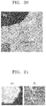
- FIG. 20 is a diagram illustrating a scanning tunneling microscopy (STM) image of a graphene layer formed according to an exemplary embodiment.
- STM scanning tunneling microscopy
- a plurality of graphenes may be formed in contact with each other on a Pt layer.
- the boundaries between the plurality of graphenes is clearly seen in the STM image.
- the structure of the graphene layer shown in FIG. 20 may be similar to the random structure described with reference to FIG. 19 .
- An enlarged view of a portion of a graphene (P-type graphene) is illustrated in a lower left corner of FIG. 20 .
- a hexagonal crystalline structure may be found in the enlarged view.
- FIG. 21 illustrates STM images of an N-type graphene formed according to an exemplary embodiment.
- View (B) of FIG. 21 is an enlarged view of a portion of view (A) of FIG. 21 , and the crystalline structure of the N-type graphene may be roughly seen in view (B) of FIG. 21 .
- the N-type graphene of FIG. 21 has a structure in which in a hexagonal crystalline structure formed from carbon (C) atoms, some of the carbon (C) atoms are substituted with nitrogen (N) atoms. That is, the STM image of view (B) of FIG. 21 may correspond to the N-type graphenes n-GP1 and n-GP2 of FIGS. 9 and 10 .
- FIGS. 22 through 26 are diagrams showing chemical structures of various source gases that may be used for forming graphenes according to the exemplary embodiments described above.
- FIG. 22 shows the chemical structure of C 5 H 5 N
- FIG. 23 shows the chemical structure of C 6 H 6
- FIG. 24 shows the chemical structure of C 2 H 4
- FIG. 25 shows the chemical structure of C 2 H 2
- FIG. 26 shows the chemical structure of C 6 H 15 B.
- Materials having chemical structures shown in FIGS. 22 through 26 may be used in the graphene layer forming methods described with reference to FIGS. 1A through 8C .
- materials (source gases) that may be used in the exemplary embodiments are not limited to those shown in FIGS. 22 through 26 , and other materials may be used as source gases.
Landscapes
- Chemical & Material Sciences (AREA)
- Engineering & Computer Science (AREA)
- Materials Engineering (AREA)
- Organic Chemistry (AREA)
- Nanotechnology (AREA)
- Inorganic Chemistry (AREA)
- Carbon And Carbon Compounds (AREA)
Claims (17)
- Verfahren zum Bilden einer Graphenschicht, das Verfahren umfassend:Bilden eines ersten Graphens auf einer ersten Region einer Unterschicht bei einer ersten Temperatur unter Verwendung eines ersten Quellgases;und Bilden eines zweiten Graphens auf einer zweiten Region anliegend an der ersten Region der Unterschicht bei einer zweiten Temperatur unter Verwendung eines zweiten Quellgases, wobei eines von dem ersten Quellgas und dem zweiten Quellgas ein Quellgas umfassend eine Kohlenwasserstoffverbindung, die Stickstoff (N) enthält, ist;wobei eines von dem ersten Graphen und dem zweiten Graphen ein p-leitendes Graphen ist, das andere von dem ersten Graphen und dem zweiten Graphen ein n-leitendes Graphen ist, das aus dem Quellgas umfassend eine Kohlenwasserstoffverbindung, die Stickstoff (N) enthält, gebildet ist, und das erste Graphen und das zweite Graphen zusammen einen p-n-Übergang bilden, wobei:das erste Quellgas und das zweite Quellgas untereinander gleich sind, und die erste Temperatur und die zweite Temperatur sich voneinander unterscheiden;oder das erste Quellgas und das zweite Quellgas sich voneinander unterscheiden, wobei das andere von dem ersten Quellgas und dem zweiten Quellgas umfassend eine Kohlenwasserstoffverbindung, die keinen Stickstoff (N) enthält, ist.
- Verfahren nach Anspruch 1, wobei das erste Quellgas und das zweite Quellgas jeweils Pyridin (C5H5N) umfassen.
- Verfahren nach Anspruch 1 oder 2, wobei die erste Temperatur größer als oder gleich wie 700 °C ist und die zweite Temperatur weniger als oder gleich wie 550 °C ist.
- Verfahren nach einem der Ansprüche 1 bis 3, wobei das erste Graphen ein p-leitendes Graphen und das zweite Graphen ein n-leitendes Graphen ist, optional wobei das n-leitende Graphen eine kristalline Struktur aufweist, die aus Kohlenstoffatomen (carbon, C) gebildet ist; wobei einige der Kohlenstoffatome (C) durch erste Atome substituiert sind, und das p-leitende Graphen eine kristalline Struktur aufweist, die nur aus Kohlenstoffatomen (C) gebildet ist, oder eine Struktur, in der einige Kohlenstoffatome (C) der kristallinen Struktur durch zweite Atome substituiert sind, die sich von den ersten Atomen unterscheiden.
- Verfahren nach Anspruch 4, wobei das erste oder zweite Graphen, das unter Verwendung einer ersten Kohlenwasserstoffverbindung gebildet ist, die keinen Stickstoff (nitrogen, N) enthält, das p-leitende Graphen ist, und das erste oder zweite Graphen, das unter Verwendung einer zweiten Kohlenwasserstoffverbindung gebildet ist, die Stickstoff (N) enthält, das n-leitende Graphen ist, optional wobei das n-leitende Graphen eine Kristallstruktur aufweist, die aus Kohlenstoffatomen (C) gebildet ist, in der einige der Kohlenstoffatome (C) durch erste Atome substituiert sind, und das p-leitende Graphen eine Kristallstruktur aufweist, die nur aus Kohlenstoffatomen (C) gebildet ist, oder eine Struktur, in der einige Kohlenstoffatome (C) der Kristallstruktur durch zweite Atome substituiert sind, die sich von den ersten Atomen unterscheiden.
- Verfahren nach Anspruch 5, wobei:die erste Kohlenwasserstoffverbindung Bor umfasst oder mindestens ein Gas umfasst, das ausgewählt ist aus der Gruppe bestehend aus Benzol (C6H6), Ethylen (C2H4), Acetylen (C2H2), und Triethylboran (C6H15B);und/oder die zweite Kohlenwasserstoffverbindung Pyridin (C5H5N) umfasst.
- Verfahren nach einem der Ansprüche 1 bis 6, wobei das erste Graphen ein p-leitendes Graphen ist, das aus Dotierungseffekten durch die Unterschicht resultiert, und das zweite Graphen ein n-leitendes Graphen ist, das aus n-leitenden Dotierstoffen aus dem zweiten Quellgas resultiert.
- Verfahren nach einem der Ansprüche 1 bis 7, wobei die Unterschicht ein katalytisches Metall umfasst, wie z. B. Platin (Pt).
- Verfahren nach einem der Ansprüche 1 bis 8, ferner umfassend ein Bilden eines dritten Graphens, das mit dem ersten Graphen oder dem zweiten Graphen verbunden ist, wobei das dritte Graphen ein p-leitendes Graphen oder ein n-leitendes Graphen ist, optional wobei die Graphenschicht eine PNP-Struktur oder eine NPN-Struktur aufweist.
- Verfahren nach einem der Ansprüche 1 bis 9, ferner umfassend ein Bilden der Unterschicht, wobei das Bilden der Unterschicht Folgendes umfasst:Bilden einer Untermaterialschicht auf einem Substrat;und Bilden einer Vielzahl von Unterschichten, die voneinander getrennt sind, durch Strukturieren der Untermaterialschicht.
- Verfahren zum Herstellen einer graphenhaltigen Vorrichtung, das Verfahren umfassend:Bilden einer Graphenschicht, umfassend einen P-N-Übergang unter Verwendung des Verfahrens nach einem der Ansprüche 1 bis 10;und Bilden eines Abschnitts der graphenhaltigen Vorrichtung, wobei der Abschnitt die Graphenschicht umfasst.
- Verfahren nach Anspruch 11, wobei die Graphenschicht auf einem ersten Substrat gebildet ist, und:
der Abschnitt der graphenhaltigen Vorrichtung auf einem zweiten Substrat gebildet wird, nachdem die Graphenschicht von dem ersten Substrat auf das zweite Substrat übertragen wurde; oder der Abschnitt der graphenhaltigen Vorrichtung auf dem ersten Substrat gebildet ist. - Graphenschicht, die durch das Verfahren nach einem der Ansprüche 1 bis 10 erlangt werden kann, umfassend:ein p-leitendes Graphen;und ein n-leitendes Graphen, das mit einer Seite des p-leitenden Graphens verbunden ist, wobei ein an einer Schnittfläche zwischen dem p-leitenden Graphen und dem n-leitenden Graphen eine Abreicherungsregion gebildet ist und eine Breite aufweist, die weniger als oder gleich wie 5 nm ist, vorzugsweise wobei die Breite der Abreicherungsregion weniger als oder gleich wie 2 nm ist.
- Graphenschicht nach Anspruch 13, wobei ein ganzer Randabschnitt der Graphenschicht eine fehlerfreie Zickzack-Struktur aufweist.
- Graphenschicht nach Anspruch 13 oder 14, wobei bei dem p-leitenden Graphen oder dem n-leitenden Graphen eine Abweichung in Dotierungskonzentration nach Region kleiner als 2,5x10¹²/cm2 ist.
- Graphenhaltige Vorrichtung, umfassend die Graphenschicht nach einem der Ansprüche 13 bis 15.
- Graphenhaltige Vorrichtung nach Anspruch 16, wobei die graphenhaltige Vorrichtung Folgendes ist:eine Diode und ferner eine erste Elektrode, die mit dem p-leitenden Graphen verbunden ist, und eine zweite Elektrode, die mit dem n-leitenden Graphen verbunden ist, umfasst; oderein Transistor und die Graphenschicht eine Kanalschicht in dem Transistor ist, optional wobei die graphenhaltige Vorrichtung eine Tunnelvorrichtung, ein Binärübergangstransistor (BJT), ein Barristor, ein Feldeffekttransistor (FET), eine Speichervorrichtung, eine Solarzelle, ein Fotodetektor, ein Sensor und eine Licht emittierende Vorrichtung ist.
Applications Claiming Priority (1)
| Application Number | Priority Date | Filing Date | Title |
|---|---|---|---|
| KR1020140150628A KR102374118B1 (ko) | 2014-10-31 | 2014-10-31 | 그래핀층 및 그 형성방법과 그래핀층을 포함하는 소자 및 그 제조방법 |
Publications (2)
| Publication Number | Publication Date |
|---|---|
| EP3015426A1 EP3015426A1 (de) | 2016-05-04 |
| EP3015426B1 true EP3015426B1 (de) | 2020-05-13 |
Family
ID=55023841
Family Applications (1)
| Application Number | Title | Priority Date | Filing Date |
|---|---|---|---|
| EP15192138.4A Active EP3015426B1 (de) | 2014-10-31 | 2015-10-29 | Graphenschicht, verfahren zur formung davon, vorrichtung mit der graphenschicht und verfahren zur herstellung der vorrichtung |
Country Status (4)
| Country | Link |
|---|---|
| US (1) | US9660036B2 (de) |
| EP (1) | EP3015426B1 (de) |
| KR (1) | KR102374118B1 (de) |
| CN (1) | CN105575769A (de) |
Families Citing this family (22)
| Publication number | Priority date | Publication date | Assignee | Title |
|---|---|---|---|---|
| KR102216542B1 (ko) * | 2014-05-21 | 2021-02-17 | 삼성전자주식회사 | 2차원 물질을 이용한 수평형 다이오드를 포함하는 전자소자 제조방법 |
| JP6439546B2 (ja) * | 2015-03-31 | 2018-12-19 | 富士通株式会社 | ガスセンサ及びその製造方法 |
| WO2017044577A1 (en) | 2015-09-08 | 2017-03-16 | Massachusetts Institute Of Technology | Systems and methods for graphene based layer transfer |
| CN105304495A (zh) * | 2015-09-21 | 2016-02-03 | 京东方科技集团股份有限公司 | 薄膜晶体管及其制备方法、阵列基板 |
| KR102446411B1 (ko) * | 2015-12-16 | 2022-09-22 | 삼성전자주식회사 | 멀티층 그래핀 및 그 형성방법과 멀티층 그래핀을 포함하는 소자 및 그 제조방법 |
| US10038060B2 (en) * | 2016-05-19 | 2018-07-31 | Qualcomm Incorporated | Graphene NMOS transistor using nitrogen dioxide chemical adsorption |
| EP3539152A4 (de) | 2016-11-08 | 2020-06-24 | Massachusetts Institute of Technology | Systeme und verfahren zur verlagerungsfilterung für schichttransfer |
| KR101862477B1 (ko) * | 2016-11-11 | 2018-05-30 | 광주과학기술원 | 쇼트키 접합 그래핀 반도체를 이용한 삼진 배리스터 |
| KR20180083641A (ko) | 2017-01-13 | 2018-07-23 | 심재훈 | 그래핀 추출방법 |
| JP6905188B2 (ja) * | 2017-07-25 | 2021-07-21 | 富士通株式会社 | 半導体装置及びその製造方法 |
| GB2570128B (en) * | 2018-01-11 | 2022-07-20 | Paragraf Ltd | A method of making a Graphene transistor and devices |
| JP2021527618A (ja) | 2018-06-22 | 2021-10-14 | マサチューセッツ インスティテュート オブ テクノロジー | グラフェンおよび/または六方晶窒化ホウ素を備えている層の上での炭化ケイ素の成長のためのシステムおよび方法ならびに関連物品 |
| CN108878268A (zh) * | 2018-07-11 | 2018-11-23 | 山东傲天环保科技有限公司 | 一种镶嵌式石墨烯pn结的制造方法 |
| WO2020072867A1 (en) * | 2018-10-05 | 2020-04-09 | Massachusetts Institute Of Technology | Methods, apparatus, and systems for remote epitaxy using stitched graphene |
| WO2020072871A1 (en) * | 2018-10-05 | 2020-04-09 | Massachusetts Institute Of Technology | Methods, apparatus, and systems for manufacturing gan templates via remote epitaxy |
| US11380763B2 (en) * | 2019-04-29 | 2022-07-05 | Arizona Board Of Regents On Behalf Of Arizona State University | Contact structures for n-type diamond |
| US20200373451A1 (en) * | 2019-05-24 | 2020-11-26 | Seven Z's Trust | Graphene and hexagonal boron nitride van der waals heterostructured solar energy processing unit (SPU) |
| CN111725322A (zh) * | 2019-08-30 | 2020-09-29 | 中国科学院上海微系统与信息技术研究所 | 一种石墨烯场效应晶体管及其制备方法和应用方法 |
| CN111244162A (zh) * | 2020-02-06 | 2020-06-05 | 西安石油大学 | 一种石墨烯同质p-n结结构及其制备方法 |
| CN112289883B (zh) * | 2020-10-30 | 2023-03-28 | 华中科技大学 | 一种三维半导体雪崩光电探测芯片及其制备方法 |
| CN114394587A (zh) * | 2021-12-13 | 2022-04-26 | 广东墨睿科技有限公司 | 一种石墨烯pn结半导体制冷片及制备方法 |
| CN116558678B (zh) * | 2023-05-16 | 2025-11-28 | 浙江农林大学 | 一种基于碳基材料的pn结型的压阻传感器制备方法 |
Family Cites Families (27)
| Publication number | Priority date | Publication date | Assignee | Title |
|---|---|---|---|---|
| US8535553B2 (en) * | 2008-04-14 | 2013-09-17 | Massachusetts Institute Of Technology | Large-area single- and few-layer graphene on arbitrary substrates |
| US7858989B2 (en) * | 2008-08-29 | 2010-12-28 | Globalfoundries Inc. | Device and process of forming device with device structure formed in trench and graphene layer formed thereover |
| US20120161098A1 (en) * | 2009-08-20 | 2012-06-28 | Nec Corporation | Substrate, manufacturing method of substrate, semiconductor element, and manufacturing method of semiconductor element |
| US8354323B2 (en) * | 2010-02-02 | 2013-01-15 | Searete Llc | Doped graphene electronic materials |
| US8278643B2 (en) * | 2010-02-02 | 2012-10-02 | Searete Llc | Doped graphene electronic materials |
| WO2011139236A1 (en) | 2010-05-05 | 2011-11-10 | National University Of Singapore | Hole doping of graphene |
| US9029836B2 (en) * | 2010-09-08 | 2015-05-12 | President And Fellows Of Harvard College | Controlled synthesis of monolithically-integrated graphene structure |
| KR101284059B1 (ko) | 2011-01-28 | 2013-07-26 | 충남대학교산학협력단 | 그라핀-산화물반도체 이종접합 소자 및 그의 제조방법 |
| KR101469450B1 (ko) | 2011-03-02 | 2014-12-05 | 그래핀스퀘어 주식회사 | 그래핀의 n-도핑 방법 |
| CN103477448B (zh) | 2011-03-29 | 2016-11-09 | 加州理工学院 | 基于石墨烯的多结柔性太阳能电池 |
| US8629427B2 (en) | 2011-04-29 | 2014-01-14 | Texas A&M University | Topological insulator-based field-effect transistor |
| CN102849961B (zh) * | 2011-07-01 | 2016-08-03 | 中央研究院 | 在基板上成长碳薄膜或无机材料薄膜的方法 |
| US8900538B2 (en) * | 2011-07-31 | 2014-12-02 | International Business Machines Corporation | Doped, passivated graphene nanomesh, method of making the doped, passivated graphene nanomesh, and semiconductor device including the doped, passivated graphene nanomesh |
| KR101813181B1 (ko) * | 2011-08-26 | 2017-12-29 | 삼성전자주식회사 | 튜너블 배리어를 포함하는 그래핀 전계효과 트랜지스터를 구비한 인버터 논리소자 |
| US8866265B2 (en) | 2011-10-03 | 2014-10-21 | The Board Of Trustees Of The Leland Stanford Junior University | Carbon-based semiconductors |
| US9040397B2 (en) * | 2011-10-21 | 2015-05-26 | LGS Innovations LLC | Method of making graphene layers, and articles made thereby |
| US9394177B2 (en) * | 2011-10-27 | 2016-07-19 | Wisconsin Alumni Research Foundation | Nanostructured graphene with atomically-smooth edges |
| US20130186758A1 (en) * | 2011-12-09 | 2013-07-25 | University Of Delaware | Current-carrying nanowire having a nanopore for high-sensitivity detection and analysis of biomolecules |
| KR101910976B1 (ko) | 2012-07-16 | 2018-10-23 | 삼성전자주식회사 | 그래핀을 이용한 전계효과 트랜지스터 |
| KR101396432B1 (ko) * | 2012-08-02 | 2014-05-21 | 경희대학교 산학협력단 | 반도체 소자 및 그의 제조 방법 |
| US8906787B2 (en) * | 2012-10-05 | 2014-12-09 | Cornell University | Thin film compositions and methods |
| CN102953118B (zh) * | 2012-11-12 | 2015-01-28 | 北京大学 | 一种单晶石墨烯pn结及其制备方法 |
| WO2014078807A2 (en) * | 2012-11-19 | 2014-05-22 | The Regents Of The University Of California | Graphene based electrodes and applications |
| KR101920724B1 (ko) * | 2012-12-11 | 2018-11-21 | 삼성전자주식회사 | 그래핀을 포함하는 전자 소자 |
| US8580658B1 (en) * | 2012-12-21 | 2013-11-12 | Solan, LLC | Methods for fabricating graphene device topography and devices formed therefrom |
| CN103268889B (zh) * | 2013-05-23 | 2016-06-01 | 清华大学 | 一种无结型横向隧穿场效应晶体管 |
| CN103280398B (zh) * | 2013-05-30 | 2016-02-03 | 中国电子科技集团公司第十三研究所 | 一种制备横向石墨烯pn结的方法 |
-
2014
- 2014-10-31 KR KR1020140150628A patent/KR102374118B1/ko not_active Expired - Fee Related
-
2015
- 2015-10-29 EP EP15192138.4A patent/EP3015426B1/de active Active
- 2015-10-29 CN CN201510717694.5A patent/CN105575769A/zh active Pending
- 2015-10-30 US US14/928,026 patent/US9660036B2/en not_active Expired - Fee Related
Non-Patent Citations (1)
| Title |
|---|
| None * |
Also Published As
| Publication number | Publication date |
|---|---|
| US9660036B2 (en) | 2017-05-23 |
| KR102374118B1 (ko) | 2022-03-14 |
| US20160126317A1 (en) | 2016-05-05 |
| CN105575769A (zh) | 2016-05-11 |
| KR20160051157A (ko) | 2016-05-11 |
| EP3015426A1 (de) | 2016-05-04 |
Similar Documents
| Publication | Publication Date | Title |
|---|---|---|
| EP3015426A1 (de) | Graphenschicht, verfahren zur formung davon, vorrichtung mit der graphenschicht und verfahren zur herstellung der vorrichtung | |
| US9006044B2 (en) | Graphene device and method of manufacturing the same | |
| CN103493216B (zh) | 形成背接触太阳能电池发射极的方法 | |
| US10224405B2 (en) | Multilayer graphene, method of forming the same, device including the multilayer graphene, and method of manufacturing the device | |
| CN102047389B (zh) | 使用ⅳ族纳米颗粒在晶片基底上形成结区 | |
| CN103730403B (zh) | 半导体结构及其形成方法 | |
| KR102395778B1 (ko) | 나노구조체 형성방법과 이를 적용한 반도체소자의 제조방법 및 나노구조체를 포함하는 반도체소자 | |
| Liu et al. | High Current density vertical tunneling transistors from graphene/highly-doped silicon heterostructures | |
| US9831452B2 (en) | Method for forming PN junction in graphene with application of DNA and PN junction structure formed using the same | |
| KR102059131B1 (ko) | 그래핀 소자 및 이의 제조 방법 | |
| US20140335681A1 (en) | Graphene transferring methods, device manufacturing method using the same, and substrate structures including graphene | |
| US9337275B2 (en) | Electrical contact for graphene part | |
| KR20110041965A (ko) | 그래핀 투명 전극 및 이를 포함하는 플렉시블 실리콘 박막 반도체 소자 | |
| CN101996870B (zh) | 掺杂方法和制造半导体器件的方法 | |
| US9396935B1 (en) | Method of fabricating ultra-thin inorganic semiconductor film and method of fabricating three-dimensional semiconductor device using the same | |
| CN117116934A (zh) | 一种具有esd保护结构的器件及其制造方法、电子装置 | |
| KR101545974B1 (ko) | 열전 소자 및 이를 제조하는 방법 | |
| CN114256147B (zh) | 半导体结构制备方法 | |
| CN103187249A (zh) | 一种半导体纳米材料器件及其制作方法 | |
| US8431462B2 (en) | Methods of manufacturing semiconductor devices | |
| CN102064099B (zh) | 栅极结构的形成方法 | |
| CN107634097B (zh) | 一种石墨烯场效应晶体管及其制造方法 | |
| CN112635325A (zh) | 一种绝缘体上应变硅/锗晶体管及其制备方法 | |
| KR101449278B1 (ko) | 반도체를 이용한 그래핀 성장 방법 | |
| US20250014898A1 (en) | Method for manufacturing nanowire, method for manufacturing thin film transistor, thin film transistor and semiconductor device |
Legal Events
| Date | Code | Title | Description |
|---|---|---|---|
| PUAI | Public reference made under article 153(3) epc to a published international application that has entered the european phase |
Free format text: ORIGINAL CODE: 0009012 |
|
| AK | Designated contracting states |
Kind code of ref document: A1 Designated state(s): AL AT BE BG CH CY CZ DE DK EE ES FI FR GB GR HR HU IE IS IT LI LT LU LV MC MK MT NL NO PL PT RO RS SE SI SK SM TR |
|
| AX | Request for extension of the european patent |
Extension state: BA ME |
|
| STAA | Information on the status of an ep patent application or granted ep patent |
Free format text: STATUS: REQUEST FOR EXAMINATION WAS MADE |
|
| 17P | Request for examination filed |
Effective date: 20161104 |
|
| RBV | Designated contracting states (corrected) |
Designated state(s): AL AT BE BG CH CY CZ DE DK EE ES FI FR GB GR HR HU IE IS IT LI LT LU LV MC MK MT NL NO PL PT RO RS SE SI SK SM TR |
|
| R17P | Request for examination filed (corrected) |
Effective date: 20161104 |
|
| STAA | Information on the status of an ep patent application or granted ep patent |
Free format text: STATUS: EXAMINATION IS IN PROGRESS |
|
| 17Q | First examination report despatched |
Effective date: 20190813 |
|
| REG | Reference to a national code |
Ref country code: DE Ref legal event code: R079 Ref document number: 602015052662 Country of ref document: DE Free format text: PREVIOUS MAIN CLASS: C01B0031040000 Ipc: C01B0032182000 |
|
| GRAP | Despatch of communication of intention to grant a patent |
Free format text: ORIGINAL CODE: EPIDOSNIGR1 |
|
| STAA | Information on the status of an ep patent application or granted ep patent |
Free format text: STATUS: GRANT OF PATENT IS INTENDED |
|
| RIC1 | Information provided on ipc code assigned before grant |
Ipc: C01B 32/182 20170101AFI20200130BHEP Ipc: H01L 51/05 20060101ALI20200130BHEP Ipc: H01L 51/00 20060101ALI20200130BHEP |
|
| INTG | Intention to grant announced |
Effective date: 20200227 |
|
| GRAS | Grant fee paid |
Free format text: ORIGINAL CODE: EPIDOSNIGR3 |
|
| GRAA | (expected) grant |
Free format text: ORIGINAL CODE: 0009210 |
|
| STAA | Information on the status of an ep patent application or granted ep patent |
Free format text: STATUS: THE PATENT HAS BEEN GRANTED |
|
| AK | Designated contracting states |
Kind code of ref document: B1 Designated state(s): AL AT BE BG CH CY CZ DE DK EE ES FI FR GB GR HR HU IE IS IT LI LT LU LV MC MK MT NL NO PL PT RO RS SE SI SK SM TR |
|
| REG | Reference to a national code |
Ref country code: GB Ref legal event code: FG4D |
|
| REG | Reference to a national code |
Ref country code: CH Ref legal event code: EP |
|
| REG | Reference to a national code |
Ref country code: DE Ref legal event code: R096 Ref document number: 602015052662 Country of ref document: DE |
|
| REG | Reference to a national code |
Ref country code: AT Ref legal event code: REF Ref document number: 1270038 Country of ref document: AT Kind code of ref document: T Effective date: 20200615 |
|
| REG | Reference to a national code |
Ref country code: LT Ref legal event code: MG4D |
|
| REG | Reference to a national code |
Ref country code: NL Ref legal event code: MP Effective date: 20200513 |
|
| PG25 | Lapsed in a contracting state [announced via postgrant information from national office to epo] |
Ref country code: FI Free format text: LAPSE BECAUSE OF FAILURE TO SUBMIT A TRANSLATION OF THE DESCRIPTION OR TO PAY THE FEE WITHIN THE PRESCRIBED TIME-LIMIT Effective date: 20200513 Ref country code: NO Free format text: LAPSE BECAUSE OF FAILURE TO SUBMIT A TRANSLATION OF THE DESCRIPTION OR TO PAY THE FEE WITHIN THE PRESCRIBED TIME-LIMIT Effective date: 20200813 Ref country code: GR Free format text: LAPSE BECAUSE OF FAILURE TO SUBMIT A TRANSLATION OF THE DESCRIPTION OR TO PAY THE FEE WITHIN THE PRESCRIBED TIME-LIMIT Effective date: 20200814 Ref country code: PT Free format text: LAPSE BECAUSE OF FAILURE TO SUBMIT A TRANSLATION OF THE DESCRIPTION OR TO PAY THE FEE WITHIN THE PRESCRIBED TIME-LIMIT Effective date: 20200914 Ref country code: IS Free format text: LAPSE BECAUSE OF FAILURE TO SUBMIT A TRANSLATION OF THE DESCRIPTION OR TO PAY THE FEE WITHIN THE PRESCRIBED TIME-LIMIT Effective date: 20200913 Ref country code: SE Free format text: LAPSE BECAUSE OF FAILURE TO SUBMIT A TRANSLATION OF THE DESCRIPTION OR TO PAY THE FEE WITHIN THE PRESCRIBED TIME-LIMIT Effective date: 20200513 Ref country code: LT Free format text: LAPSE BECAUSE OF FAILURE TO SUBMIT A TRANSLATION OF THE DESCRIPTION OR TO PAY THE FEE WITHIN THE PRESCRIBED TIME-LIMIT Effective date: 20200513 |
|
| PG25 | Lapsed in a contracting state [announced via postgrant information from national office to epo] |
Ref country code: HR Free format text: LAPSE BECAUSE OF FAILURE TO SUBMIT A TRANSLATION OF THE DESCRIPTION OR TO PAY THE FEE WITHIN THE PRESCRIBED TIME-LIMIT Effective date: 20200513 Ref country code: LV Free format text: LAPSE BECAUSE OF FAILURE TO SUBMIT A TRANSLATION OF THE DESCRIPTION OR TO PAY THE FEE WITHIN THE PRESCRIBED TIME-LIMIT Effective date: 20200513 Ref country code: BG Free format text: LAPSE BECAUSE OF FAILURE TO SUBMIT A TRANSLATION OF THE DESCRIPTION OR TO PAY THE FEE WITHIN THE PRESCRIBED TIME-LIMIT Effective date: 20200813 Ref country code: RS Free format text: LAPSE BECAUSE OF FAILURE TO SUBMIT A TRANSLATION OF THE DESCRIPTION OR TO PAY THE FEE WITHIN THE PRESCRIBED TIME-LIMIT Effective date: 20200513 |
|
| REG | Reference to a national code |
Ref country code: AT Ref legal event code: MK05 Ref document number: 1270038 Country of ref document: AT Kind code of ref document: T Effective date: 20200513 |
|
| PG25 | Lapsed in a contracting state [announced via postgrant information from national office to epo] |
Ref country code: NL Free format text: LAPSE BECAUSE OF FAILURE TO SUBMIT A TRANSLATION OF THE DESCRIPTION OR TO PAY THE FEE WITHIN THE PRESCRIBED TIME-LIMIT Effective date: 20200513 Ref country code: AL Free format text: LAPSE BECAUSE OF FAILURE TO SUBMIT A TRANSLATION OF THE DESCRIPTION OR TO PAY THE FEE WITHIN THE PRESCRIBED TIME-LIMIT Effective date: 20200513 |
|
| PG25 | Lapsed in a contracting state [announced via postgrant information from national office to epo] |
Ref country code: ES Free format text: LAPSE BECAUSE OF FAILURE TO SUBMIT A TRANSLATION OF THE DESCRIPTION OR TO PAY THE FEE WITHIN THE PRESCRIBED TIME-LIMIT Effective date: 20200513 Ref country code: AT Free format text: LAPSE BECAUSE OF FAILURE TO SUBMIT A TRANSLATION OF THE DESCRIPTION OR TO PAY THE FEE WITHIN THE PRESCRIBED TIME-LIMIT Effective date: 20200513 Ref country code: EE Free format text: LAPSE BECAUSE OF FAILURE TO SUBMIT A TRANSLATION OF THE DESCRIPTION OR TO PAY THE FEE WITHIN THE PRESCRIBED TIME-LIMIT Effective date: 20200513 Ref country code: IT Free format text: LAPSE BECAUSE OF FAILURE TO SUBMIT A TRANSLATION OF THE DESCRIPTION OR TO PAY THE FEE WITHIN THE PRESCRIBED TIME-LIMIT Effective date: 20200513 Ref country code: DK Free format text: LAPSE BECAUSE OF FAILURE TO SUBMIT A TRANSLATION OF THE DESCRIPTION OR TO PAY THE FEE WITHIN THE PRESCRIBED TIME-LIMIT Effective date: 20200513 Ref country code: RO Free format text: LAPSE BECAUSE OF FAILURE TO SUBMIT A TRANSLATION OF THE DESCRIPTION OR TO PAY THE FEE WITHIN THE PRESCRIBED TIME-LIMIT Effective date: 20200513 Ref country code: SM Free format text: LAPSE BECAUSE OF FAILURE TO SUBMIT A TRANSLATION OF THE DESCRIPTION OR TO PAY THE FEE WITHIN THE PRESCRIBED TIME-LIMIT Effective date: 20200513 Ref country code: CZ Free format text: LAPSE BECAUSE OF FAILURE TO SUBMIT A TRANSLATION OF THE DESCRIPTION OR TO PAY THE FEE WITHIN THE PRESCRIBED TIME-LIMIT Effective date: 20200513 |
|
| REG | Reference to a national code |
Ref country code: DE Ref legal event code: R097 Ref document number: 602015052662 Country of ref document: DE |
|
| PG25 | Lapsed in a contracting state [announced via postgrant information from national office to epo] |
Ref country code: PL Free format text: LAPSE BECAUSE OF FAILURE TO SUBMIT A TRANSLATION OF THE DESCRIPTION OR TO PAY THE FEE WITHIN THE PRESCRIBED TIME-LIMIT Effective date: 20200513 Ref country code: SK Free format text: LAPSE BECAUSE OF FAILURE TO SUBMIT A TRANSLATION OF THE DESCRIPTION OR TO PAY THE FEE WITHIN THE PRESCRIBED TIME-LIMIT Effective date: 20200513 |
|
| PLBE | No opposition filed within time limit |
Free format text: ORIGINAL CODE: 0009261 |
|
| STAA | Information on the status of an ep patent application or granted ep patent |
Free format text: STATUS: NO OPPOSITION FILED WITHIN TIME LIMIT |
|
| 26N | No opposition filed |
Effective date: 20210216 |
|
| PG25 | Lapsed in a contracting state [announced via postgrant information from national office to epo] |
Ref country code: SI Free format text: LAPSE BECAUSE OF FAILURE TO SUBMIT A TRANSLATION OF THE DESCRIPTION OR TO PAY THE FEE WITHIN THE PRESCRIBED TIME-LIMIT Effective date: 20200513 |
|
| REG | Reference to a national code |
Ref country code: CH Ref legal event code: PL |
|
| PG25 | Lapsed in a contracting state [announced via postgrant information from national office to epo] |
Ref country code: LU Free format text: LAPSE BECAUSE OF NON-PAYMENT OF DUE FEES Effective date: 20201029 Ref country code: MC Free format text: LAPSE BECAUSE OF FAILURE TO SUBMIT A TRANSLATION OF THE DESCRIPTION OR TO PAY THE FEE WITHIN THE PRESCRIBED TIME-LIMIT Effective date: 20200513 |
|
| REG | Reference to a national code |
Ref country code: BE Ref legal event code: MM Effective date: 20201031 |
|
| PG25 | Lapsed in a contracting state [announced via postgrant information from national office to epo] |
Ref country code: BE Free format text: LAPSE BECAUSE OF NON-PAYMENT OF DUE FEES Effective date: 20201031 Ref country code: CH Free format text: LAPSE BECAUSE OF NON-PAYMENT OF DUE FEES Effective date: 20201031 Ref country code: LI Free format text: LAPSE BECAUSE OF NON-PAYMENT OF DUE FEES Effective date: 20201031 |
|
| PG25 | Lapsed in a contracting state [announced via postgrant information from national office to epo] |
Ref country code: IE Free format text: LAPSE BECAUSE OF NON-PAYMENT OF DUE FEES Effective date: 20201029 |
|
| PGFP | Annual fee paid to national office [announced via postgrant information from national office to epo] |
Ref country code: FR Payment date: 20210930 Year of fee payment: 7 |
|
| PGFP | Annual fee paid to national office [announced via postgrant information from national office to epo] |
Ref country code: GB Payment date: 20210922 Year of fee payment: 7 |
|
| PG25 | Lapsed in a contracting state [announced via postgrant information from national office to epo] |
Ref country code: TR Free format text: LAPSE BECAUSE OF FAILURE TO SUBMIT A TRANSLATION OF THE DESCRIPTION OR TO PAY THE FEE WITHIN THE PRESCRIBED TIME-LIMIT Effective date: 20200513 Ref country code: MT Free format text: LAPSE BECAUSE OF FAILURE TO SUBMIT A TRANSLATION OF THE DESCRIPTION OR TO PAY THE FEE WITHIN THE PRESCRIBED TIME-LIMIT Effective date: 20200513 Ref country code: CY Free format text: LAPSE BECAUSE OF FAILURE TO SUBMIT A TRANSLATION OF THE DESCRIPTION OR TO PAY THE FEE WITHIN THE PRESCRIBED TIME-LIMIT Effective date: 20200513 |
|
| PG25 | Lapsed in a contracting state [announced via postgrant information from national office to epo] |
Ref country code: MK Free format text: LAPSE BECAUSE OF FAILURE TO SUBMIT A TRANSLATION OF THE DESCRIPTION OR TO PAY THE FEE WITHIN THE PRESCRIBED TIME-LIMIT Effective date: 20200513 |
|
| PGFP | Annual fee paid to national office [announced via postgrant information from national office to epo] |
Ref country code: DE Payment date: 20220621 Year of fee payment: 8 |
|
| GBPC | Gb: european patent ceased through non-payment of renewal fee |
Effective date: 20221029 |
|
| PG25 | Lapsed in a contracting state [announced via postgrant information from national office to epo] |
Ref country code: FR Free format text: LAPSE BECAUSE OF NON-PAYMENT OF DUE FEES Effective date: 20221031 |
|
| PG25 | Lapsed in a contracting state [announced via postgrant information from national office to epo] |
Ref country code: GB Free format text: LAPSE BECAUSE OF NON-PAYMENT OF DUE FEES Effective date: 20221029 |
|
| REG | Reference to a national code |
Ref country code: DE Ref legal event code: R119 Ref document number: 602015052662 Country of ref document: DE |
|
| PG25 | Lapsed in a contracting state [announced via postgrant information from national office to epo] |
Ref country code: DE Free format text: LAPSE BECAUSE OF NON-PAYMENT OF DUE FEES Effective date: 20240501 |