EP3005415B1 - Haltevorrichtung, verfahren zu deren herstellung und verwendung derselben - Google Patents
Haltevorrichtung, verfahren zu deren herstellung und verwendung derselben Download PDFInfo
- Publication number
- EP3005415B1 EP3005415B1 EP14741791.9A EP14741791A EP3005415B1 EP 3005415 B1 EP3005415 B1 EP 3005415B1 EP 14741791 A EP14741791 A EP 14741791A EP 3005415 B1 EP3005415 B1 EP 3005415B1
- Authority
- EP
- European Patent Office
- Prior art keywords
- retainer
- coating
- silicon
- plasma
- substrates
- Prior art date
- Legal status (The legal status is an assumption and is not a legal conclusion. Google has not performed a legal analysis and makes no representation as to the accuracy of the status listed.)
- Not-in-force
Links
Images


Classifications
-
- H—ELECTRICITY
- H10—SEMICONDUCTOR DEVICES; ELECTRIC SOLID-STATE DEVICES NOT OTHERWISE PROVIDED FOR
- H10P—GENERIC PROCESSES OR APPARATUS FOR THE MANUFACTURE OR TREATMENT OF DEVICES COVERED BY CLASS H10
- H10P72/00—Handling or holding of wafers, substrates or devices during manufacture or treatment thereof
- H10P72/70—Handling or holding of wafers, substrates or devices during manufacture or treatment thereof for supporting or gripping
- H10P72/76—Handling or holding of wafers, substrates or devices during manufacture or treatment thereof for supporting or gripping using mechanical means, e.g. clamps or pinches
- H10P72/7604—Handling or holding of wafers, substrates or devices during manufacture or treatment thereof for supporting or gripping using mechanical means, e.g. clamps or pinches the wafers being placed on a susceptor, stage or support
- H10P72/7616—Handling or holding of wafers, substrates or devices during manufacture or treatment thereof for supporting or gripping using mechanical means, e.g. clamps or pinches the wafers being placed on a susceptor, stage or support characterised by a coating, a hardness or a material
-
- C—CHEMISTRY; METALLURGY
- C23—COATING METALLIC MATERIAL; COATING MATERIAL WITH METALLIC MATERIAL; CHEMICAL SURFACE TREATMENT; DIFFUSION TREATMENT OF METALLIC MATERIAL; COATING BY VACUUM EVAPORATION, BY SPUTTERING, BY ION IMPLANTATION OR BY CHEMICAL VAPOUR DEPOSITION, IN GENERAL; INHIBITING CORROSION OF METALLIC MATERIAL OR INCRUSTATION IN GENERAL
- C23C—COATING METALLIC MATERIAL; COATING MATERIAL WITH METALLIC MATERIAL; SURFACE TREATMENT OF METALLIC MATERIAL BY DIFFUSION INTO THE SURFACE, BY CHEMICAL CONVERSION OR SUBSTITUTION; COATING BY VACUUM EVAPORATION, BY SPUTTERING, BY ION IMPLANTATION OR BY CHEMICAL VAPOUR DEPOSITION, IN GENERAL
- C23C16/00—Chemical coating by decomposition of gaseous compounds, without leaving reaction products of surface material in the coating, i.e. chemical vapour deposition [CVD] processes
- C23C16/22—Chemical coating by decomposition of gaseous compounds, without leaving reaction products of surface material in the coating, i.e. chemical vapour deposition [CVD] processes characterised by the deposition of inorganic material, other than metallic material
- C23C16/30—Deposition of compounds, mixtures or solid solutions, e.g. borides, carbides, nitrides
- C23C16/32—Carbides
- C23C16/325—Silicon carbide
-
- C—CHEMISTRY; METALLURGY
- C23—COATING METALLIC MATERIAL; COATING MATERIAL WITH METALLIC MATERIAL; CHEMICAL SURFACE TREATMENT; DIFFUSION TREATMENT OF METALLIC MATERIAL; COATING BY VACUUM EVAPORATION, BY SPUTTERING, BY ION IMPLANTATION OR BY CHEMICAL VAPOUR DEPOSITION, IN GENERAL; INHIBITING CORROSION OF METALLIC MATERIAL OR INCRUSTATION IN GENERAL
- C23C—COATING METALLIC MATERIAL; COATING MATERIAL WITH METALLIC MATERIAL; SURFACE TREATMENT OF METALLIC MATERIAL BY DIFFUSION INTO THE SURFACE, BY CHEMICAL CONVERSION OR SUBSTITUTION; COATING BY VACUUM EVAPORATION, BY SPUTTERING, BY ION IMPLANTATION OR BY CHEMICAL VAPOUR DEPOSITION, IN GENERAL
- C23C16/00—Chemical coating by decomposition of gaseous compounds, without leaving reaction products of surface material in the coating, i.e. chemical vapour deposition [CVD] processes
- C23C16/44—Chemical coating by decomposition of gaseous compounds, without leaving reaction products of surface material in the coating, i.e. chemical vapour deposition [CVD] processes characterised by the method of coating
- C23C16/50—Chemical coating by decomposition of gaseous compounds, without leaving reaction products of surface material in the coating, i.e. chemical vapour deposition [CVD] processes characterised by the method of coating using electric discharges
-
- F—MECHANICAL ENGINEERING; LIGHTING; HEATING; WEAPONS; BLASTING
- F28—HEAT EXCHANGE IN GENERAL
- F28F—DETAILS OF HEAT-EXCHANGE AND HEAT-TRANSFER APPARATUS, OF GENERAL APPLICATION
- F28F13/00—Arrangements for modifying heat-transfer, e.g. increasing, decreasing
- F28F13/18—Arrangements for modifying heat-transfer, e.g. increasing, decreasing by applying coatings, e.g. radiation-absorbing, radiation-reflecting; by surface treatment, e.g. polishing
-
- H—ELECTRICITY
- H10—SEMICONDUCTOR DEVICES; ELECTRIC SOLID-STATE DEVICES NOT OTHERWISE PROVIDED FOR
- H10F—INORGANIC SEMICONDUCTOR DEVICES SENSITIVE TO INFRARED RADIATION, LIGHT, ELECTROMAGNETIC RADIATION OF SHORTER WAVELENGTH OR CORPUSCULAR RADIATION
- H10F71/00—Manufacture or treatment of devices covered by this subclass
-
- H—ELECTRICITY
- H10—SEMICONDUCTOR DEVICES; ELECTRIC SOLID-STATE DEVICES NOT OTHERWISE PROVIDED FOR
- H10F—INORGANIC SEMICONDUCTOR DEVICES SENSITIVE TO INFRARED RADIATION, LIGHT, ELECTROMAGNETIC RADIATION OF SHORTER WAVELENGTH OR CORPUSCULAR RADIATION
- H10F71/00—Manufacture or treatment of devices covered by this subclass
- H10F71/137—Batch treatment of the devices
-
- H—ELECTRICITY
- H10—SEMICONDUCTOR DEVICES; ELECTRIC SOLID-STATE DEVICES NOT OTHERWISE PROVIDED FOR
- H10F—INORGANIC SEMICONDUCTOR DEVICES SENSITIVE TO INFRARED RADIATION, LIGHT, ELECTROMAGNETIC RADIATION OF SHORTER WAVELENGTH OR CORPUSCULAR RADIATION
- H10F77/00—Constructional details of devices covered by this subclass
- H10F77/30—Coatings
- H10F77/306—Coatings for devices having potential barriers
- H10F77/311—Coatings for devices having potential barriers for photovoltaic cells
-
- H—ELECTRICITY
- H10—SEMICONDUCTOR DEVICES; ELECTRIC SOLID-STATE DEVICES NOT OTHERWISE PROVIDED FOR
- H10P—GENERIC PROCESSES OR APPARATUS FOR THE MANUFACTURE OR TREATMENT OF DEVICES COVERED BY CLASS H10
- H10P14/00—Formation of materials, e.g. in the shape of layers or pillars
- H10P14/60—Formation of materials, e.g. in the shape of layers or pillars of insulating materials
- H10P14/63—Formation of materials, e.g. in the shape of layers or pillars of insulating materials characterised by the formation processes
- H10P14/6326—Deposition processes
- H10P14/6328—Deposition from the gas or vapour phase
- H10P14/6334—Deposition from the gas or vapour phase using decomposition or reaction of gaseous or vapour phase compounds, i.e. chemical vapour deposition
- H10P14/6336—Deposition from the gas or vapour phase using decomposition or reaction of gaseous or vapour phase compounds, i.e. chemical vapour deposition in the presence of a plasma [PECVD]
-
- H—ELECTRICITY
- H10—SEMICONDUCTOR DEVICES; ELECTRIC SOLID-STATE DEVICES NOT OTHERWISE PROVIDED FOR
- H10P—GENERIC PROCESSES OR APPARATUS FOR THE MANUFACTURE OR TREATMENT OF DEVICES COVERED BY CLASS H10
- H10P14/00—Formation of materials, e.g. in the shape of layers or pillars
- H10P14/60—Formation of materials, e.g. in the shape of layers or pillars of insulating materials
- H10P14/69—Inorganic materials
- H10P14/692—Inorganic materials composed of oxides, glassy oxides or oxide-based glasses
- H10P14/6921—Inorganic materials composed of oxides, glassy oxides or oxide-based glasses containing silicon
- H10P14/69215—Inorganic materials composed of oxides, glassy oxides or oxide-based glasses containing silicon the material being a silicon oxide, e.g. SiO2
-
- H—ELECTRICITY
- H10—SEMICONDUCTOR DEVICES; ELECTRIC SOLID-STATE DEVICES NOT OTHERWISE PROVIDED FOR
- H10P—GENERIC PROCESSES OR APPARATUS FOR THE MANUFACTURE OR TREATMENT OF DEVICES COVERED BY CLASS H10
- H10P14/00—Formation of materials, e.g. in the shape of layers or pillars
- H10P14/60—Formation of materials, e.g. in the shape of layers or pillars of insulating materials
- H10P14/69—Inorganic materials
- H10P14/692—Inorganic materials composed of oxides, glassy oxides or oxide-based glasses
- H10P14/6921—Inorganic materials composed of oxides, glassy oxides or oxide-based glasses containing silicon
- H10P14/6922—Inorganic materials composed of oxides, glassy oxides or oxide-based glasses containing silicon the material containing Si, O and at least one of H, N, C, F or other non-metal elements, e.g. SiOC, SiOC:H or SiONC
- H10P14/6927—Inorganic materials composed of oxides, glassy oxides or oxide-based glasses containing silicon the material containing Si, O and at least one of H, N, C, F or other non-metal elements, e.g. SiOC, SiOC:H or SiONC the material being a silicon oxynitride, e.g. SiON or SiON:H
-
- H—ELECTRICITY
- H10—SEMICONDUCTOR DEVICES; ELECTRIC SOLID-STATE DEVICES NOT OTHERWISE PROVIDED FOR
- H10P—GENERIC PROCESSES OR APPARATUS FOR THE MANUFACTURE OR TREATMENT OF DEVICES COVERED BY CLASS H10
- H10P14/00—Formation of materials, e.g. in the shape of layers or pillars
- H10P14/60—Formation of materials, e.g. in the shape of layers or pillars of insulating materials
- H10P14/69—Inorganic materials
- H10P14/694—Inorganic materials composed of nitrides
- H10P14/6943—Inorganic materials composed of nitrides containing silicon
- H10P14/69433—Inorganic materials composed of nitrides containing silicon the material being a silicon nitride not containing oxygen, e.g. SixNy or SixByNz
-
- H—ELECTRICITY
- H10—SEMICONDUCTOR DEVICES; ELECTRIC SOLID-STATE DEVICES NOT OTHERWISE PROVIDED FOR
- H10P—GENERIC PROCESSES OR APPARATUS FOR THE MANUFACTURE OR TREATMENT OF DEVICES COVERED BY CLASS H10
- H10P72/00—Handling or holding of wafers, substrates or devices during manufacture or treatment thereof
- H10P72/70—Handling or holding of wafers, substrates or devices during manufacture or treatment thereof for supporting or gripping
- H10P72/76—Handling or holding of wafers, substrates or devices during manufacture or treatment thereof for supporting or gripping using mechanical means, e.g. clamps or pinches
- H10P72/7604—Handling or holding of wafers, substrates or devices during manufacture or treatment thereof for supporting or gripping using mechanical means, e.g. clamps or pinches the wafers being placed on a susceptor, stage or support
-
- H—ELECTRICITY
- H10—SEMICONDUCTOR DEVICES; ELECTRIC SOLID-STATE DEVICES NOT OTHERWISE PROVIDED FOR
- H10P—GENERIC PROCESSES OR APPARATUS FOR THE MANUFACTURE OR TREATMENT OF DEVICES COVERED BY CLASS H10
- H10P72/00—Handling or holding of wafers, substrates or devices during manufacture or treatment thereof
- H10P72/70—Handling or holding of wafers, substrates or devices during manufacture or treatment thereof for supporting or gripping
- H10P72/76—Handling or holding of wafers, substrates or devices during manufacture or treatment thereof for supporting or gripping using mechanical means, e.g. clamps or pinches
- H10P72/7604—Handling or holding of wafers, substrates or devices during manufacture or treatment thereof for supporting or gripping using mechanical means, e.g. clamps or pinches the wafers being placed on a susceptor, stage or support
- H10P72/7621—Handling or holding of wafers, substrates or devices during manufacture or treatment thereof for supporting or gripping using mechanical means, e.g. clamps or pinches the wafers being placed on a susceptor, stage or support characterised by supporting two or more semiconductor substrates
Definitions
- the invention relates to a holding device, a method for producing the holding device and their use.
- PECVD plasma-enhanced chemical vapor deposition
- silicon solar cell substrates are often arranged in these boats, which are sometimes referred to as PECVD boats, and provided with an anti-reflection layer of silicon nitride as part of a PECVD deposition.
- PECVD boats silicon solar cell substrates are often arranged in these boats, which are sometimes referred to as PECVD boats, and provided with an anti-reflection layer of silicon nitride as part of a PECVD deposition.
- homogeneous antireflection layers are only obtained if the boat used has previously been provided with a silicon nitride layer.
- the boats used are therefore coated with silicon nitride as part of a so-called silicon nitride pre-assignment, before a coating of solar cell substrates arranged in the boats is carried out with silicon nitride.
- the material used for the boats is usually graphite.
- silicon nitride is electrically insulating as a dielectric and for the PECVD deposition of silicon nitride on the silicon solar cell substrates
- an electrically conductive contact between the boat and the arranged therein silicon solar cell substrates is required in silicon nitride Vorbelegung those areas in which the silicon solar cell substrates on the boat for Coming to be omitted from the silicon nitride pre-assignment.
- This is usually achieved by arranging silicon substrates in these regions during the silicon nitride prepreg, which are usually referred to as dummy wafers and largely prevent silicon nitride deposition on retaining lugs or portions of the booster surface covered by the dummy wafers in said regions.
- retaining lugs are to be understood projections on the surfaces of the boats, on which the silicon solar cell substrates are supported.
- the retaining lugs contribute significantly to the electrical contacting, since the silicon substrates often do not rest with sufficient surface area on the boat used during Siliziumnidritabscheidungen.
- oxygen-containing gases are present in a PECVD deposition, for example when nitrous oxide or nitrogen monoxide is used as the process gas, the silicon nitride pre-assignment can not cause the boats to be decomposed in those areas which were shielded by the dummy wafers during the silicon nitride pre-assignment prevent.
- RTP rapid thermal processing
- the described Decomposition in oxygen-containing process gas atmospheres leads to wear of the holding device used. Reference will still be made to the documents JP2008034729 . US2002047122 . JPH11186181 and JP2000164522 ,
- the present invention according to the independent device claim 1 is therefore based on the object to provide a holding device is available, which has an improved wear resistance in oxygen-containing process gas atmospheres.
- the invention has the object to enable a low-cost coating of substrates.
- This object is achieved by a use of the holding device according to the invention according to claim 6.
- the invention has for its object to provide a low-cost method for producing the holding device according to the invention.
- This object is achieved by a method having the features of claim 9.
- Advantageous developments are each the subject of dependent claims.
- the holding device according to the invention has on its surface a coating of silicon carbide, glassy carbon or pyrolytic carbon. With holders coated in this way, increased wear resistance in oxygen-containing process gas atmospheres can be realized. This is especially true for oxygenated Process gas atmospheres, which are formed using nitrous oxide and / or nitrogen monoxide as process gases.
- the stated coating materials can in principle be applied in any manner known per se.
- a glassy carbon coating can be applied by mixing phenolic resin powder in an alcohol bath and immersing the article to be coated in the resulting solution. Subsequently, the object to be coated is heated to a temperature of at least 600 ° C. This procedure has proven particularly useful for graphite articles to be coated.
- a coating of silicon carbide is provided.
- Silicon carbide is abrasion resistant and resistant to hydrofluoric acid. In most applications, it is therefore very rarely necessary to re-coat silicon carbide.
- silicon carbide adheres well to graphite, which is a common material for semiconductor devices. Further, it has been found that graphite bodies having a silicon carbide coating have similar surface electric resistance as silicon solar cell substrates. This seems to have an advantageous effect on the properties of layers deposited by means of PECVD processes on silicon solar cell substrates. However, morphological or chemical reasons or the porosity or grain size of the graphite may also play a role here.
- the silicon nitride prepreg described above can be dispensed with in silicon carbide-coated holding devices, in particular in the case of silicon carbide-coated boats, without the homogeneity of a silicon nitride layer deposited using such a holding device, for example a Antireflection coating, thereby being affected to a relevant extent.
- silicon carbide is electrically conductive, the above-described dummy wafers are not needed. In the industrial production of silicon solar cells, the need for dummy wafers is a not inconsiderable cost factor, so that the use of the holding device according to the invention and the associated need for dummy wafers makes it possible to reduce the manufacturing outlay.
- Silicon carbide or a silicon carbide coating is to be understood here as meaning that the material used or the coating concerned consists essentially of silicon carbide. A perfect purity of the material is not required. Contaminants, foreign material entries at interfaces or other may be present in practically conventional amounts.
- retaining devices according to the invention are used in silicon nitride deposits, silicon nitride is deposited on the holding device used as well. After a certain number of deposits, spalling of silicon nitride parts from the fixture occurs. As a result, the quality of the silicon nitride layer can be impaired, which is deposited on an object arranged in the holding device. For this reason, holders of silicon nitride deposition equipment are usually etched back after a certain number of deposits. It has been found that when using a holding device according to the invention, the number of possible deposits before a next Ruharm is required, compared to previously known holding devices can be increased. This is the case in particular with holding devices which have a coating of silicon carbide. The higher number of with a holding device until the next pollharmgang feasible Siliziumnitridabborgungen allows in industrial applications, for example in industrial solar cell production, a further reduction of manufacturing costs.
- the holding device is provided with a coating of pyrolytic carbon, an improved resistance to oxygen and oxygen radicals results compared to a coating with glassy carbon at high temperatures of up to 1100 ° C.
- a pyrolytically deposited carbon layer may be combined by pyrolytically deposited carbon infiltration. Such a combination adheres very well to graphite and is very dense. Furthermore, it has a much harder surface than a simple pyrolytically deposited carbon layer and is more resistant to oxygen and oxygen radicals. Accordingly, such fixtures are more resistant to mechanical stress and more resistant to degradation in oxygenated process environments.
- the holding device consists predominantly of graphite or glass.
- it is entirely made of graphite or glass.
- the glass mentioned may in particular be a quartz glass.
- graphite has proven particularly useful, which is why this material is particularly preferred.
- the coating is advantageously arranged directly on a core material of the holding device. Pre or intermediate coatings can be omitted in this way.
- the coating extends over the entire surface of the holding device, so that the increased wear resistance is present over the entire surface of the holding device. If the holding device is designed as a graphite boat, then the coating preferably extends over all electrically conductive surface portions of the graphite boat.
- a silicon carbide coating with a thickness of less than 25 ⁇ m is provided as the coating.
- the thickness is less than 10 microns, and more preferably, the thickness has a maximum value of 10 microns and a minimum value of 1 micron.
- the thickness of the silicon carbide coating thus varies in an interval with a lower interval limit of 1 ⁇ m and an upper interval limit of 10 ⁇ m. It has been shown that with such configured silicon carbide coatings, the wear resistance of the holding device can be increased particularly efficiently.
- the holding device is designed as a boat for Dampfabscheideanlagen.
- the vapor deposition equipment may be physical vapor deposition (PVD) or chemical vapor deposition (CVD) equipment.
- the boat is adapted to receive silicon substrates.
- the boat is designed to be suitable for use in PECVD installations.
- the holding device is designed as a susceptor for RTP furnaces.
- RTP furnaces are ovens which are suitable for the rapid thermal processing of objects, in particular of semiconductor substrates. Become a PRT stoves often heated by means of halogen lamps and allow a very rapid heating of the object.
- the use according to the invention provides that a holding device designed as a boat for vapor deposition systems is used as a holding device for substrates in a plasma-driven deposition from the gas phase. In this way, the substrates can be coated at low cost, since the holding device has an increased wear resistance in an oxygen-containing process gas atmosphere.
- the holding device is used for silicon substrates and more preferably for silicon solar cell substrates.
- silicon substrates in particular in the case of the use of boats in which the coating is formed of silicon carbide, in the case of silicon nitride deposition, silicon nitride pre-emption is dispensed with and the use of dummy wafers is dispensed with.
- silicon nitride or silicon oxynitride is deposited on the substrates, preferably silicon nitride.
- silicon nitride or silicon oxynitride is deposited on the substrates, preferably silicon nitride.
- the boat can be used particularly advantageously in those PECVD deposits in which at least temporarily an oxygen-containing process gas atmosphere is formed.
- this is advantageous because in this way their wear can be reduced. Therefore, in PECVD silica deposition, the use of the boat has proven advantageous.
- the advantages offered by the use according to the invention according to current knowledge, regardless of whether the coating takes place at about atmospheric pressure or lower pressures, regardless of whether it is an ionic or radical type of coating and also independent of the plasma frequency used.
- the use according to the invention in combination with plasma frequencies of less than 400 kHz and especially in connection with a plasma frequency of 40 kHz and in conjunction with a plasma frequency of 13.56 kHz or 2.45 GHz has proved particularly useful.
- the method for producing a holding device according to the invention provides for depositing silicon carbide as a coating on a bulk material of the holding device by means of a chemical vapor deposition.
- the term bulk material is to be understood as meaning the material of which the holding device consists before application of the coating. If the holding device before the application of the coating is not made of a uniform material, the term volume material thus includes all materials that make up the holding device at this time, with the exception of joining parts such as spacers or connecting elements. In particular, any previously applied additional coatings are included.
- the holding device can be provided at low cost with the coating. This is particularly the case when the holding device is intended for use in a CVD system. Because in this case, this CVD system, which can be performed for example as a PECVD system, both for coating the fixture can be used as well as for the coating of later in the fixture arranged objects. These items may be, for example, substrates.
- Such a coating of the holding device with silicon carbide is much more cost effective than an external CVD deposition.
- Existing CVD, or PECVD plants usually have to be modified only slightly to allow the silicon carbide deposition. For example, in the case of a PECVD system already applied for a silicon nitride separation, only one supply device for methane is to be additionally provided.
- the coating is deposited on a bulk material which predominantly, preferably completely, consists of graphite or glass.
- a bulk material which predominantly, preferably completely, consists of graphite or glass.
- These materials have proven themselves in practice and can be used in many applications as holding devices, especially in applications of semiconductor device manufacturing.
- Particular preference is given to coating a bulk material consisting mainly or entirely of graphite, since this material is generally better suited for use in PECVD systems because of its electrical conductivity.
- the deposition of the silicon carbide is preferably carried out by means of a plasma-driven deposition from the gas phase or in other words by means of a PECVD deposition.
- a direct plasma is advantageously formed on a surface of the holding device. This has changed especially proven to be advantageous when the direct plasma is formed on a graphite surface.
- a plasma formed using methane and silane can be used.
- a plasma is used, which is formed from methane and silane.
- the deposited silicon carbide is compacted. This can be effected for example by means of an ion bombardment and is particularly preferably realized by means of a plasma.
- a low-frequency plasma with a plasma frequency of less than 400 kHz has proven particularly useful.
- FIG. 1 Illustrates a schematic perspective view of an embodiment of a boat 10 for Dampfabscheideanlagen, in this case for a PECVD system running holding device.
- the boat 10 is adapted to receive silicon substrates and in particular silicon solar cell substrates and is composed in a conventional manner of a plurality of plates 14 a, 14 b, 14 c and other plates.
- three retaining lugs 16 are provided for each of the silicon substrates.
- the bulk material of the boat 10 is in the embodiment of FIG. 1 except for graphite insulators 15, on which a silicon carbide coating 12 is directly disposed.
- silicon carbide could also Glassy carbon or pyrolytic carbon may be provided.
- the coating 12 extends, apart from the insulators 15 used as spacers and thus as spacer elements, over the entire surface of the boat 10 and has a thickness between 1 .mu.m and 10 .mu.m.
- FIG. 2 shows a schematic plan view of an embodiment of a designed as a susceptor 50 for RTP furnaces holding device in a schematic representation.
- the susceptor 50 has on its surface a coating 12 of silicon carbide, which extends over the entire surface of the susceptor 52 and has a thickness between 1 .mu.m and 10 .mu.m.
- the susceptor consists entirely of graphite or glass.
- the coating may also be formed of glassy carbon or pyrolytic carbon.
- the coating 52 is disposed directly on a bulk material of the susceptor 50, which is made of graphite or glass in the manner mentioned. This is explained in more detail below with reference to the illustration in FIG. 3 explained.
- FIG. 3 shows a schematic partial sectional view through the susceptor 50 FIG. 2 , or by the boat 10 FIG. 1 , In the case of the boat 10 off FIG. 1 could FIG. 3 for example, represent a partial section through the plate 14a.
- FIG. 3 shows a bulk material 60, which is provided on all surfaces with a coating 62. Becomes FIG. 3 as a partial section through the boat 10 off FIG. 1 understood, the coating 62, the silicon carbide coating 52 from FIG. 1 and the bulk material 60 is graphite. Becomes FIG. 3 on the other hand as a partial sectional view through FIG. 2 Thus, the coating 62 represents the silicon carbide coating 52 and the bulk material 60 is graphite or glass.
- the volume material 60 also represents the core material of the boat 10 or of the susceptor 50, respectively. Pre or intermediate coatings are not present.
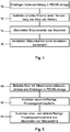
- FIG. 4 shows a schematic diagram of an embodiment of the method according to the invention.
- a holding device such as a boat or a susceptor
- a direct plasma is formed on a surface of the holding device 72. It takes place
- Deposition 74 of silicon carbide by means of a plasma-driven deposition from the gas phase.
- the deposited silicon carbide is densified by ion bombardment 76.
- the ions used for this purpose are preferably generated by means of a low-frequency plasma plasma.
- FIG. 5 Illustrates a schematic representation of an embodiment of the use according to the invention.
- an oxygen-containing process gas atmosphere is formed 92, in which in the present embodiment, a Siliziumoxinitrid für is formed on the silicon solar cell substrates.
- a silane- and nitrogen-containing process gas atmosphere is formed, and silicon nitride in the form of a silicon nitride-containing layer is deposited on the silicon solar cell substrates 93.
- FIG Embodiment of FIG. 5 is used as a boat in FIG. 1 illustrated, provided with a coating 12 of silicon carbide and a graphite volume material having boat 10 so that the boat 10 is protected against premature wear in the oxygen-containing process gas atmosphere by the coating 12 of silicon carbide.
- this embodiment can be dispensed with a silicon nitride pre-assignment of the boat 10 as well as the material-consuming use of dummy wafers.
- the embodiment of FIG. 5 thus allows a cost-effective coating of the silicon solar cell substrates with silicon nitride, for example as an anti-reflection coating.
Landscapes
- Chemical & Material Sciences (AREA)
- Engineering & Computer Science (AREA)
- Mechanical Engineering (AREA)
- Physics & Mathematics (AREA)
- Materials Engineering (AREA)
- Organic Chemistry (AREA)
- Metallurgy (AREA)
- General Chemical & Material Sciences (AREA)
- Chemical Kinetics & Catalysis (AREA)
- Plasma & Fusion (AREA)
- General Engineering & Computer Science (AREA)
- Thermal Sciences (AREA)
- Inorganic Chemistry (AREA)
- Chemical Vapour Deposition (AREA)
- Life Sciences & Earth Sciences (AREA)
- Sustainable Development (AREA)
- Sustainable Energy (AREA)
- Manufacturing & Machinery (AREA)
- Photovoltaic Devices (AREA)
- Container, Conveyance, Adherence, Positioning, Of Wafer (AREA)
Description
- Die Erfindung betrifft eine Haltevorrichtung, ein Verfahren zur Herstellung der Haltevorrichtung sowie deren Verwendung.
- Bei der Herstellung von Halbleiterbauelementen, insbesondere von Siliziumsolarzellen, werden häufig plasmagetriebene Abscheidungen aus der Gasphase durchgeführt, welche im englischen Sprachraum als plasma-enhanced chemical vapor deposition (PECVD) bezeichnet werden. Hierbei sind die zu beschichtenden Halbleitersubstrate üblicherweise in Haltevorrichtungen angeordnet. Bei PECVD-Abscheidungen werden regelmäßig sogenannte Boote als Haltevorrichtungen eingesetzt.
- Bei der industriellen Fertigung von Siliziumsolarzellen werden häufig Siliziumsolarzellensubstrate in diesen Booten, welche teilweise auch als PECVD-Boote bezeichnet werden, angeordnet und im Rahmen einer PECVD-Abscheidung mit einer Antireflexionsschicht aus Siliziumnitrid versehen. Homogene Antireflexionsschichten erhält man jedoch nur, wenn das verwendete Boot zuvor bereits mit einer Siliziumnitridschicht versehen wurde. Üblicherweise werden die eingesetzten Boote daher im Rahmen einer sogenannten Siliziumnitrid-Vorbelegung mit Siliziumnitrid beschichtet, ehe eine Beschichtung von in den Booten angeordneten Solarzellensubstraten mit Siliziumnitrid durchgeführt wird. Als Material für die Boote wird üblicherweise Graphitverwendet. Möglicherweise ist das Erfordernis der Siliziumnitrid-Vorbelegung darauf zurückzuführen, dass die elektrischen Oberflächenwiderstände von Graphit und den Siliziumsolarzellensubstraten zu unterschiedlich sind. Es können jedoch auch morphologische oder chemische Gründe, die Porosität des Bootmaterials oder dessen Korngrößenbeschaffenheit eine Rolle spielen. Die Ursachen sind derzeit nicht abschließend geklärt.
- Da Siliziumnitrid als Dielektrikum elektrisch isolierend wirkt und für die PECVD-Abscheidung von Siliziumnitrid auf den Siliziumsolarzellensubstraten ein elektrisch leitender Kontakt zwischen dem Boot und den darin angeordneten Siliziumsolarzellensubstraten erforderlich ist, müssen bei der Siliziumnitrid-Vorbelegung diejenigen Bereiche, in welchen die Siliziumsolarzellensubstrate an dem Boot zur Anlage kommen, von der Siliziumnitrid-Vorbelegung ausgespart werden. Dies wird üblicherweise realisiert, indem in diesen Bereichen während der Siliziumnitrid-Vorbelegung Siliziumsubstrate angeordnet werden, welche üblicherweise als Dummy-Wafer bezeichnet werden und in den genannten Bereichen eine Siliziumnitridabscheidung auf Haltenasen oder von den Dummy-Wafern bedeckten Abschnitten der Bootoberfläche weitgehend verhindern. Unter Haltenasen sind dabei Vorsprünge an den Oberflächen der Boote zu verstehen, an welchen die Siliziumsolarzellensubstrate abgestützt werden. Die Haltenasen tragen wesentlich zur elektrischen Kontaktierung bei, da die Siliziumsubstrate während Siliziumnidritabscheidungen häufig nicht mit ausreichender Fläche an dem verwendeten Boot anliegen.
- Sind bei einer PECVD-Abscheidung sauerstoffhaltige Gase vorhanden, beispielsweise bei einem Einsatz von Lachgas oder Stickstoffmonoxid als Prozessgas, so kann die Siliziumnitrid-Vorbelegung eine Zersetzung der Boote in denjenigen Bereichen, welche während der Siliziumnitrid-Vorbelegung durch die Dummy-Wafer abgeschirmt waren, nicht verhindern. Dies gilt in gleicher Weise für andere Haltevorrichtungen, wie beispielsweise in Schnellbearbeitungsanlagen, sogenannten Rapid Thermal Processing (RTP)-Anlagen verwendete Suszeptoren. Die beschriebene Zersetzung in sauerstoffhaltigen Prozessgasatmosphären führt zum Verschleiß der eingesetzten Haltevorrichtung. Es wird noch Bezug genommen auf die Dokumente
JP2008034729 US2002047122 ,JPH11186181 JP2000164522 - Der vorliegenden Erfindung gemäss dem unabhängigen Vorrichtungsanspruch 1 liegt daher die Aufgabe zugrunde, eine Haltevorrichtung zur Verfügung zu stellen, welche in sauerstoffhaltigen Prozessgasatmosphären eine verbesserte Verschleißbeständigkeit aufweist.
- Weiterhin liegt der Erfindung die Aufgabe zugrunde, eine aufwandsgünstige Beschichtung von Substraten zu ermöglichen. Diese Aufgabe wird gelöst durch eine Verwendung der erfindungsgemäßen Haltevorrichtung gemäß Anspruch 6. Ferner liegt der Erfindung die Aufgabe zugrunde, ein aufwandsgünstiges Verfahren zur Herstellung der erfindungsgemäßen Haltevorrichtung zur Verfügung zu stellen.
Diese Aufgabe wird gelöst durch ein Verfahren mit den Merkmalen des Anspruchs 9.
Vorteilhafte Weiterbildungen sind jeweils Gegenstand abhängiger Unteransprüche.
Die erfindungsgemäße Haltevorrichtung weist an ihrer Oberfläche eine Beschichtung aus Siliziumkarbid, Glaskohlenstoff oder pyrolytischem Kohlenstoff auf.
Mit derart beschichteten Haltevorrichtungen kann eine erhöhte Verschleißbeständigkeit in sauerstoffhaltigen Prozessgasatmosphären realisiert werden. Dies ist insbesondere bei sauerstoffhaltigen Prozessgasatmosphären der Fall, welche unter Verwendung von Lachgas und/oder Stickstoffmonoxid als Prozessgasen gebildet werden. - Die genannten Beschichtungsmaterialien können grundsätzlich auf jede an sich bekannte Weise aufgebracht werden. Eine Beschichtung aus Glaskohlenstoff kann beispielsweise aufgebracht werden, indem einem Alkoholbad Phenolharzpulver beigemischt und der zu beschichtende Gegenstand in die resultierende Lösung eingetaucht wird. Nachfolgend wird der zu beschichtende Gegenstand auf eine Temperatur von mindestens 600°C erwärmt. Diese Vorgehensweise hat sich insbesondere bei zu beschichtenden Gegenständen aus Graphit bewährt.
- Vorzugsweise wird eine Beschichtung aus Siliziumkarbid vorgesehen. Siliziumkarbid ist abriebfest und gegenüber Flusssäure beständig. In den meisten Anwendungsfällen bedarf es somit nur sehr selten einer Nachbeschichtung mit Siliziumkarbid. Des Weiteren haftet Siliziumkarbid gut auf Graphit, welches ein gängiges Material für in der Halbleitertechnik eingesetzte Haltevorrichtungen ist. Ferner hat sich gezeigt, dass Graphitkörper mit einer Siliziumkarbidbeschichtung einen ähnlichen elektrischen Oberflächenwiderstand aufweisen wie Siliziumsolarzellensubstrate. Dies scheint sich vorteilhaft auf die Eigenschaften von mittels PECVD-Verfahren auf Siliziumsolarzellensubstraten abgeschiedene Schichten auszuwirken. Jedoch können auch morphologische oder chemische Gründe oder die Porosität oder die Korngrößenbeschaffenheit des Graphits hierbei eine Rolle spielen. Jedenfalls hat sich gezeigt, dass die eingangs beschriebene Siliziumnitrid-Vorbelegung bei siliziumkarbidbeschichteten Haltevorrichtungen, insbesondere bei siliziumkarbidbeschichteten Booten, entfallen kann, ohne dass die Homogenität einer unter Verwendung solch einer Haltevorrichtung abgeschiedenen Siliziumnitridschicht, beispielsweise einer Antireflexionsbeschichtung, hierdurch in relevantem Umfang beeinträchtigt wird. Da Siliziumkarbid elektrisch leitfähig ist, werden zudem die oben beschriebenen Dummy-Wafer nicht benötigt. Bei der industriellen Fertigung von Siliziumsolarzellen ist der Bedarf an Dummy-Wafern ein nicht vernachlässigbarer Kostenfaktor, sodass der Einsatz der erfindungsgemäßen Haltevorrichtung und der damit entfallende Bedarf an Dummy-Wafern eine Reduktion des Fertigungsaufwandes ermöglicht.
- Unter Siliziumkarbid beziehungsweise einer Siliziumkarbidbeschichtung ist vorliegend zu verstehen, dass das eingesetzte Material beziehungsweise die betroffene Beschichtung im Wesentlichen aus Siliziumkarbid besteht. Eine vollkommene Reinheit des Werkstoffes ist nicht erforderlich. Verunreinigungen, Fremdmaterialeinträge an Grenzflächen oder anderes können in praktisch üblichen Mengen vorhanden sein.
- Werden erfindungsgemäße Haltevorrichtungen bei Siliziumnitridabscheidungen eingesetzt, so wird auch auf der verwendeten Haltevorrichtung Siliziumnitrid abgeschieden. Nach einer gewissen Anzahl von Abscheidungen kommt es zu Abplatzungen von Siliziumnitridteilen von der Haltevorrichtung. Hierdurch kann die Qualität der Siliziumnitridschicht beeinträchtigt werden, welche auf einem in der Haltevorrichtung angeordneten Objekt abgeschieden wird. Aus diesem Grund werden Haltevorrichtungen von Siliziumnitridabscheideanlagen üblicherweise nach einer gewissen Zahl von Abscheidungen zurückgeätzt. Es hat sich gezeigt, dass bei der Verwendung einer erfindungsgemäßen Haltevorrichtung die Zahl der möglichen Abscheidungen, bevor ein nächster Rückätzschritt erforderlich ist, gegenüber bislang bekannten Haltevorrichtungen erhöht werden kann. Dies ist insbesondere bei Haltevorrichtungen der Fall, welche eine Beschichtung aus Siliziumkarbid aufweisen. Die höhere Zahl der mit einer Haltevorrichtung bis zum nächsten Rückätzvorgang durchführbaren Siliziumnitridabscheidungen ermöglicht in der industriellen Anwendung, beispielsweise bei der industriellen Solarzellenfertigung, eine weitere Reduktion des Fertigungsaufwandes.
- Ist die Haltevorrichtung mit einer Beschichtung aus pyrolytischem Kohlenstoff versehen, so ergibt sich gegenüber einer Beschichtung mit Glaskohlenstoff bei hohen Temperaturen von bis zu 1100°C eine verbesserte Resistenz gegenüber Sauerstoff und Sauerstoffradikalen. Eine pyrolytisch abgeschiedene Kohlenstoffschicht kann durch eine Infiltration mit pyrolytisch abgeschiedenem Kohlenstoff kombiniert werden. Eine derartige Kombination haftet sehr gut auf Graphit und ist sehr dicht. Ferner weist sie gegenüber einer einfachen pyrolytisch abgeschiedenen Kohlenstoffschicht eine deutlich härtere Oberfläche auf und ist resistenter gegenüber Sauerstoff und Sauerstoffradikalen. Derartige Haltevorrichtungen sind dementsprechend verschleißfester gegenüber mechanischen Beanspruchungen und widerstandsfähiger gegenüber einer Zersetzung in sauerstoffhaltigen Prozessumgebungen.
- Eine Weiterbildung sieht vor, dass die Haltevorrichtung überwiegend aus Graphit oder Glas besteht. Vorzugsweise besteht sie, abgesehen von der Beschichtung, vollständig aus Graphit oder Glas. Bei dem genannten Glas kann es sich insbesondere um ein Quarzglas handeln. In der Praxis hat sich, insbesondere bei der Herstellung von Halbleiterbauelementen, Graphit besonders bewährt, weswegen dieses Material besonders bevorzugt wird.
- Die Beschichtung ist vorteilhaftweise unmittelbar auf einem Kernmaterial der Haltevorrichtung angeordnet. Vor- oder Zwischenbeschichtungen können auf diese Weise entfallen.
- Vorteilhafterweise erstreckt sich die Beschichtung über die gesamte Oberfläche der Haltevorrichtung, sodass die erhöhte Verschleißbeständigkeit über die gesamte Oberfläche der Haltevorrichtung hinweg vorliegt. Ist die Haltevorrichtung als Graphitboot ausgeführt, so erstreckt sich die Beschichtung vorzugsweise über sämtliche elektrisch leitfähigen Oberflächenanteile des Graphitboots.
- In einer besonders bevorzugten Ausgestaltungsvariante ist als Beschichtung eine Siliziumkarbidbeschichtung vorgesehen mit einer Dicke von weniger als 25 µm. Vorzugsweise ist die Dicke geringer als 10 µm und besonders bevorzugt weist die Dicke einen Maximalwert von 10 µm und einem Minimalwert von 1 µm auf. Im letztgenannten Fall variiert die Dicke der Siliziumkarbidbeschichtung somit in einem Intervall mit einer unteren Intervallgrenze von 1 µm und einer oberen Intervallgrenze von 10 µm. Es hat sich gezeigt, dass bei derart ausgestalteten Siliziumkarbidbeschichtungen die Verschleißbeständigkeit der Haltevorrichtung besonders effizient erhöht werden kann.
- In einer Ausgestaltungsvariante ist die Haltevorrichtung als Boot für Dampfabscheideanlagen ausgeführt. Bei den Dampfabscheideanlagen kann es sich um physikalische (physical vapour deposition - PVD) oder chemische Dampfabscheideanlagen (chemical vapour deposition - CVD) handeln. Vorzugsweise ist das Boot dazu geeignet, Siliziumsubstrate aufzunehmen. Besonders bevorzugt wird das Boot derart ausgelegt, dass es zur Verwendung in PECVD-Anlagen geeignet ist.
- In einer anderen Ausführungsvariante ist die Haltevorrichtung als Suszeptor für RTP-Öfen ausgeführt. Unter RTP-Öfen sind dabei Öfen zu verstehen, welche zur schnellen thermischen Bearbeitung (rapid thermal processing) von Gegenständen, insbesondere von Halbleitersubstraten, geeignet sind. PRT-Öfen werden häufig mittels Halogenlampen beheizt und ermöglichen ein sehr schnelles Erwärmen des Gegenstandes.
- Die erfindungsgemäße Verwendung sieht vor, dass eine als Boot für Dampfabscheideanlagen ausgeführte Haltevorrichtung bei einer plasmagetriebenen Abscheidung aus der Gasphase als Haltevorrichtung für Substrate verwendet wird. Auf diese Weise können die Substrate aufwandsgünstig beschichtet werden, da die Haltevorrichtung eine erhöhte Verschleißbeständigkeit in sauerstoffhaltiger Prozessgasatmosphäre aufweist.
- Vorzugsweise wird die Haltevorrichtung für Siliziumsubstrate und besonders bevorzugt für Siliziumsolarzellensubstrate verwendet. Auf diese Weise kann, insbesondere bei der Verwendung von Booten, bei welchen die Beschichtung aus Siliziumkarbid gebildet ist, im Falle einer Siliziumnitridabscheidung auf eine Siliziumnitrid-Vorbelegung verzichtet und von einem Einsatz von Dummy-Wafern abgesehen werden. Diese Sachverhalte wurden oben bereits im Zusammenhang mit der Haltevorrichtung näher erläutert. Im Ergebnis können somit Siliziumsubstrate, beziehungsweise Siliziumsolarzellensubstrate, aufwandsgünstiger beschichtet werden.
- Vorteilhafterweise wird daher bei der plasmagetriebenen Abscheidung aus der Gasphase Siliziumnitrid oder Siliziumoxinitrid auf den Substraten abgeschieden, vorzugsweise Siliziumnitrid. Insbesondere bei einer Abscheidung auf Siliziumsubstraten, beziehungsweise Siliziumsolarzellensubstraten, kann auf diese Weise eine deutliche Reduktion des Fertigungsaufwands bewirkt werden.
- Aufgrund der erhöhten Verschleißbeständigkeit der Haltevorrichtung in einer sauerstoffhaltigen Prozessgasatmosphäre kann das Boot besonders vorteilhaft verwendet werden bei denjenigen PECVD-Abscheidungen, bei welchen zumindest zeitweise eine sauerstoffhaltige Prozessgasatmosphäre ausgebildet wird. Insbesondere im Fall einer Verwendung von Graphitbooten ist dies von Vorteil, da auf diese Weise deren Verschleiß verringert werden kann. Bei PECVD-Siliziumoxidabscheidungen hat sich die Verwendung des Bootes daher als vorteilhaft erwiesen.
- Die Vorteile, welche die erfindungsgemäße Verwendung bietet, stellen sich nach jetzigem Kenntnisstand unabhängig davon ein, ob die Beschichtung in etwa bei Atmosphärendruck oder geringeren Druckwerten erfolgt, unabhängig davon ob es sich um eine ionische oder radikale Beschichtungsart handelt und auch unabhängig von der verwendeten Plasmafrequenz. Besonders bewährt hat sich die erfindungsgemäße Verwendung in Verbindung mit Plasmafrequenzen kleiner als 400 kHz und ganz besonders in Verbindung mit einer Plasmafrequenz von 40 kHz sowie in Verbindung mit einer Plasmafrequenz von 13,56 kHz oder 2,45 GHz.
- Das Verfahren zur Herstellung einer erfindungsgemäßen Haltevorrichtung sieht vor, mittels einer chemischen Abscheidung aus der Gasphase Siliziumkarbid als Beschichtung auf einem Volumenmaterial der Haltevorrichtung abzuscheiden.
- Unter dem Begriff des Volumenmaterials ist vorliegend das Material zu verstehen, aus dem die Haltevorrichtung vor Aufbringung der Beschichtung besteht. Sofern die Haltevorrichtung vor dem Aufbringen der Beschichtung nicht aus einem einheitlichen Material besteht, umfasst der Begriff des Volumenmaterials somit sämtliche Materialien, aus denen die Haltevorrichtung zu diesem Zeitpunkt besteht, mit Ausnahme von Fügeteilen wie beispielsweise Distanzelementen oder Verbindungselementen. Insbesondere sind etwaige zuvor bereits aufgebrachte Zusatzbeschichtungen eingeschlossen.
- Mit dem beschriebenen Verfahren kann die Haltevorrichtung aufwandsgünstig mit der Beschichtung versehen werden. Dies ist insbesondere dann der Fall, wenn die Haltevorrichtung zur Verwendung in einer CVD-Anlage vorgesehen ist. Denn in diesem Fall kann diese CVD-Anlage, die beispielsweise als PECVD-Anlage ausgeführt sein kann, sowohl zur Beschichtung der Haltevorrichtung verwendet werden wie auch zur Beschichtung von später in der Haltevorrichtung angeordneten Gegenständen. Bei diesen Gegenständen kann es sich zum Beispiel um Substrate handeln. Eine derartige Beschichtung der Haltevorrichtung mit Siliziumkarbid ist wesentlich aufwandsgünstiger als eine externe CVD-Abscheidung. Bereits vorhandene CVD-, beziehungsweise PECVD-, Anlagen müssen in der Regel nur geringfügig modifiziert werden um die Siliziumkarbidabscheidung zu ermöglichen. Im Falle einer bereits für eine Siliziumnitridabscheidung angerichteten PECVD-Anlage ist beispielsweise lediglich eine Zuführvorrichtung für Methan zusätzlich vorzusehen.
- Vorteilhafterweise wird die Beschichtung auf einem Volumenmaterial abgeschieden, welches überwiegend, vorzugsweise vollständig, aus Graphit oder Glas besteht. Diese Materialien haben sich in der Praxis bewährt und können in vielen Anwendungsfällen als Haltevorrichtungen eingesetzt werden, insbesondere in Anwendungsfällen der Halbleiterbauelementfertigung. Besonders bevorzugt wird ein überwiegend oder vollständig aus Graphit bestehendes Volumenmaterial beschichtet, da dieses Material für den Einsatz in PECVD-Anlagen aufgrund seiner elektrischen Leitfähigkeit im Regelfall besser geeignet ist.
- Die Abscheidung des Siliziumkarbids erfolgt bevorzugt mittels einer plasmagetriebenen Abscheidung aus der Gasphase oder in anderen Worten mittels einer PECVD-Abscheidung. Für die Abscheidung wird vorteilhafterweise ein direktes Plasma an einer Oberfläche der Haltevorrichtung ausgebildet. Dies hat sich insbesondere als dann als vorteilhaft erwiesen, wenn das direkte Plasma an einer Graphitoberfläche ausgebildet wird.
- Für die Abscheidung des Siliziumkarbids kann ein unter Verwendung von Methan und Silan gebildetes Plasma verwendet werden. Vorzugsweise kommt ein Plasma zum Einsatz, welches aus Methan und Silan gebildet wird.
- In einer vorteilhaften Ausführungsvariante wird das abgeschiedene Siliziumkarbid verdichtet. Dies kann beispielsweise mittels eines Ionenbombardements bewirkt werden und wird besonders bevorzugt mittels eines Plasmas realisiert. Besonders bewährt hat sich in diesem Zusammenhang ein Niederfrequenzplasma mit einer Plasmafrequenz kleiner als 400 kHz.
- Im Weiteren wird die Erfindung anhand von Figuren näher erläutert. Soweit zweckdienlich, sind hierin gleichwirkende Elemente mit gleichen Bezugszeichen versehen. Die Erfindung ist nicht auf die in den Figuren dargestellten Ausführungsbeispiele beschränkt - auch nicht in Bezug auf funktionale Merkmale. Die bisherige Beschreibung wie auch die nachfolgende Figurenbeschreibung enthalten zahlreiche Merkmale, die in den abhängigen Unteransprüchen teilweise zu mehreren zusammengefasst wiedergegeben sind. Diese Merkmale wie auch alle übrigen oben und in der nachfolgenden Figurenbeschreibung offenbarte Merkmale wird der Fachmann jedoch auch Einzeln betrachten und zu sinnvollen weiteren Kombinationen zusammenfügen. Insbesondere sind diese Merkmale jeweils einzeln und in beliebiger geeigneter Kombination mit der Haltevorrichtung und/oder dem Verfahren und/oder der Verwendung gemäß den unabhängigen Ansprüchen kombinierbar. Es zeigen:
- Figur 1
- Ein Ausführungsbeispiel einer als Boot für Dampfabscheideanlagen ausgeführten Haltevorrichtung in schematischer Darstellung
- Figur 2
- Ein Ausführungsbeispiel einer als Suszeptor für RTP-Öfen ausgeführten Haltevorrichtung in schematischer Darstellung
- Figur 3
- Schematische Teilschnittdarstellung durch die Haltevorrichtung gemäß
Figur 2 beziehungsweise durch die Haltevorrichtung ausFigur 1 - Figur 4
- Ein Ausführungsbeispiel des erfindungsgemäßen Verfahrens
- Figur 5
- Ein Ausführungsbeispiel der erfindungsgemäßen Verwendung
-
Figur 1 illustriert in einer schematischen Perspektivdarstellung ein Ausführungsbeispiel einer als Boot 10 für Dampfabscheideanlagen, vorliegend für eine PECVD-Anlage, ausgeführten Haltevorrichtung. Das Boot 10 ist dazu geeignet, Siliziumsubstrate und insbesondere Siliziumsolarzellensubstrate aufzunehmen und ist in an sich bekannter Weise aus mehreren Platten 14a, 14b, 14c sowie weiteren Platten zusammengesetzt. Zur Aufnahme von Siliziumsubstraten sind für jedes der Siliziumsubstrate drei Haltenasen 16 vorgesehen. - Das Volumenmaterial des Bootes 10 besteht im Ausführungsbeispiel der
Figur 1 , abgesehen von Isolatoren 15, aus Graphit, auf welchem unmittelbar eine Beschichtung 12 aus Siliziumkarbid angeordnet ist. Anstelle von Siliziumkarbid könnte auch Glaskohlenstoff oder pyrolytischer Kohlenstoff vorgesehen sein. - Die Beschichtung 12 erstreckt sich, abgesehen von den als Abstandshaltern und somit als Distanzelemente verwendeten Isolatoren 15, über die gesamte Oberfläche des Bootes 10 und weist eine Dicke zwischen 1 µm und 10 µm auf.
-
Figur 2 zeigt in einer schematischen Aufsichtdarstellung ein Ausführungsbeispiel einer als Suszeptor 50 für RTP-Öfen ausgeführten Haltevorrichtung in schematischer Darstellung. Der Suszeptor 50 weist an seiner Oberfläche eine Beschichtung 12 aus Siliziumkarbid auf, welche sich über die gesamte Oberfläche des Suszeptors 52 erstreckt und eine Dicke zwischen 1 µm und 10 µm aufweist. Abgesehen von der Beschichtung 52 besteht der Suszeptor vollständig aus Graphit oder Glas. Anstelle der Beschichtung 52 aus Siliziumkarbid kann die Beschichtung auch aus Glaskohlenstoff oder pyrolytischem Kohlenstoff gebildet sein. - Die Beschichtung 52 ist unmittelbar auf einem Volumenmaterial des Suszeptors 50 angeordnet, welches in der erwähnten Weise aus Graphit oder Glas besteht. Dies wird nachfolgend näher anhand der Darstellung in
Figur 3 erläutert. -
Figur 3 zeigt eine schematische Teilschnittdarstellung durch den Suszeptor 50 ausFigur 2 , beziehungsweise durch das Boot 10 ausFigur 1 . Im Falle des Boots 10 ausFigur 1 könnteFigur 3 beispielsweise einen Teilschnitt durch die Platte 14a darstellen.Figur 3 zeigt ein Volumenmaterial 60, welches an allen Oberflächen mit einer Beschichtung 62 versehen ist. WirdFigur 3 als Teilschnittdarstellung durch das Boot 10 ausFigur 1 aufgefasst, so stellt die Beschichtung 62 die Siliziumkarbidbeschichtung 52 ausFigur 1 dar und bei dem Volumenmaterial 60 handelt es sich um Graphit. WirdFigur 3 andererseits als Teilschnittdarstellung durchFigur 2 aufgefasst, so stellt die Beschichtung 62 die Beschichtung 52 aus Siliziumkarbid dar und das Volumenmaterial 60 ist Graphit oder Glas. In den Ausführungsbeispielen derFiguren 1 bis 3 stellt das Volumenmaterial 60 jeweils auch das Kernmaterial des Bootes 10 beziehungsweise des Suszeptors 50 dar. Vor- oder Zwischenbeschichtungen sind nicht vorhanden. -
Figur 4 zeigt eine Prinzipdarstellung eines Ausführungsbeispiels des erfindungsgemäßen Verfahrens. Bei diesem wird zunächst eine Haltevorrichtung, beispielsweise ein Boot oder ein Suszeptor, in eine PECVD-Anlage eingebracht 70. Im Weiteren wird in der PECVD-Anlage unter Verwendung von Silan und Methan ein direktes Plasma an einer Oberfläche der Haltevorrichtung ausgebildet 72. Es erfolgt eine Abscheidung 74 von Siliziumkarbid mittels einer plasmagetriebenen Abscheidung aus der Gasphase. Darüber hinaus wird das abgeschiedene Siliziumkarbid durch Ionenbombardement verdichtet 76. Die hierfür eingesetzten Ionen werden vorzugsweise mittels eines Niederfrequenzplasmas Plasma erzeugt. -
Figur 5 illustriert in einer Prinzipdarstellung ein Ausführungsbeispiel der erfindungsgemäßen Verwendung. Hierbei wird eine als Boot für Dampfabscheideanlagen ausgeführte Haltevorrichtung mit Siliziumsolarzellensubstraten beladen und in eine PECVD-Anlage eingebracht 90. In dieser PECVD-Anlage wird eine sauerstoffhaltige Prozessgasatmosphäre ausgebildet 92, in welcher im vorliegenden Ausführungsbeispiel eine Siliziumoxinitridschicht auf den Siliziumsolarzellensubstraten ausgebildet wird. Im Weiteren wird eine silan- und stickstoffhaltige Prozessgasatmosphäre ausgebildet und hierin Siliziumnitrid in Gestalt einer siliziumnitridhaltigen Schicht auf den Siliziumsolarzellensubstraten abgeschieden 93. In dem dargestellten Ausführungsbeispiel derFigur 5 wird als Boot das inFigur 1 dargestellte, mit einer Beschichtung 12 aus Siliziumkarbid versehene und ein Volumenmaterial aus Graphit aufweisende Boot 10 verwendet, sodass das Boot 10 gegenüber einem vorzeitigen Verschleiß in der sauerstoffhaltigen Prozessgasatmosphäre durch die Beschichtung 12 aus Siliziumkarbid geschützt ist. Wie oben dargelegt wurde, kann bei dieser Ausführungsvariante auf eine Siliziumnitrid-Vorbelegung des Bootes 10 ebenso verzichtet werden wie auf den materialaufwändigen Einsatz von Dummy-Wafern. Das Ausführungsbeispiel derFigur 5 ermöglicht somit eine aufwandsgünstige Beschichtung der Siliziumsolarzellensubstrate mit Siliziumnitrid, beispielsweise als Antireflexionsbeschichtung. -
- 10
- Boot
- 12
- Beschichtung
- 14a
- Platte
- 14b
- Platte
- 14c
- Platte
- 15
- Isolator
- 16
- Haltenasen
- 50
- Suszeptor
- 52
- Beschichtung
- 60
- Volumenmaterial
- 62
- Beschichtung
- 70
- Einbringen Haltevorrichtung in PECVD-Anlage
- 72
- Ausbilden Plasma unter Verwendung von Silan und Methan
- 74
- Abscheiden Siliziumkarbid aus Gasphase
- 76
- Verdichten Siliziumkarbid durch Ionenbombardement mittels des Plasmas
- 90
- Beladen Boot mit Siliziumsolarzellensubstraten und Einbringen in PECVD-Anlage
- 92
- Ausbilden sauerstoffhaltige Prozessgasatmosphäre und Abscheiden von Siliziumnitrid
- 93
- Ausbilden silan- und stickstoffhaltige Prozessgasatmosphäre und Abscheiden von Siliziumnitrid
Claims (14)
- Haltevorrichtung (10; 50) für Halbleitersubstrate wobei- die Haltevorrichtung (10; 50) an ihrer Oberfläche eine Beschichtung (12; 52) aus Siliziumkarbid aufweist; und- die Beschichtung (62) unmittelbar auf einem Kernmaterial (60) der Haltevorrichtung (10; 50) angeordnet ist;dadurch gekennzeichnet,
dass eine Dicke der Siliziumkarbidbeschichtung einen Maximalwert von 10 µm und einen Minimalwert von 1 µm aufweist. - Haltevorrichtung (10; 50) nach Anspruch 1,
dadurch gekennzeichnet,
dass die Haltevorrichtung (10; 50) überwiegend, vorzugsweise bis auf die Beschichtung (12; 52) vollständig, aus Graphit oder Glas besteht. - Haltevorrichtung (10; 50) nach einem der vorangegangenen Ansprüche,
dadurch gekennzeichnet,
dass die Beschichtung sich über die gesamte Oberfläche der Haltevorrichtung (50) erstreckt. - Haltevorrichtung (10) nach einem der vorangegangenen Ansprüche,
dadurch gekennzeichnet,
dass die Haltevorrichtung (10) als Boot (10) für Dampfabscheideanlagen ausgeführt ist, welches vorzugsweise dazu geeignet ist, Siliziumsubstrate aufzunehmen. - Haltevorrichtung (50) nach einem der Ansprüche 1 bis 3,
dadurch gekennzeichnet,
dass die Haltevorrichtung (50) als Suszeptor (50) für RTP-Öfen ausgeführt ist. - Verwendung (90, 92) eines Bootes (10) nach Anspruch 4 bei einer plasmagetriebenen Abscheidung aus der Gasphase als Haltevorrichtung (10) für Substrate, vorzugsweise für Siliziumsubstrate und besonders bevorzugt für Siliziumsolarzellensubstrate.
- Verwendung (90, 92) nach Anspruch 6,
dadurch gekennzeichnet,
dass bei der plasmagetriebenen Abscheidung aus der Gasphase Silziumoxid, Siliziumoxinitrid oder Siliziumnitrid auf den Substraten abgeschieden wird (92), vorzugsweise Siliziumnitrid. - Verwendung (90, 92) nach einem der Ansprüche 6 bis 7,
dadurch gekennzeichnet,
dass bei der plasmagetriebenen Abscheidung aus der Gasphase zumindest zweitweise eine sauerstoffhaltige Prozessgasatmosphäre ausgebildet wird (92). - Verfahren zur Herstellung einer Haltevorrichtung (10; 52) gemäß einem der Ansprüche 1 bis 5,
bei welchem mittels einer chemischen Abscheidung aus der Gasphase (14) Siliziumkarbid als Beschichtung (12; 52, 62) auf einem Volumenmaterial (60) der Haltevorrichtung (10;
50) abgeschieden wird (14);
dadurch gekennzeichnet,
dass das abgeschiedene Siliziumkarbid verdichtet wird (76). - Verfahren nach Anspruch 9,
dadurch gekennzeichnet,
dass die Beschichtung (12; 52; 62) auf einem Volumenmaterial (60) abgeschieden wird (14), welches überwiegend, vorzugsweise vollständig, aus Graphit oder Glas besteht. - Verfahren nach einem der Ansprüche 9 bis 10,
dadurch gekennzeichnet,
dass die Abscheidung (14) mittels einer plasmagetriebenen Abscheidung aus der Gasphase erfolgt. - Verfahren nach Anspruch 11,
dadurch gekennzeichnet,
dass das für die Abscheidung (14) verwendete Plasma in Gestalt eines direkten Plasmas an einer Oberfläche der zu beschichtenden Haltevorrichtung (10; 52) ausgebildet wird. - Verfahren nach einem der Ansprüche 11 bis 12,
dadurch gekennzeichnet,
dass für die Abscheidung (14) ein unter Verwendung von Methan und Silan gebildetes (12) Plasma verwendet wird. - Verfahren nach einem der Ansprüche 9 bis 13,
dadurch gekennzeichnet,
dass das abgeschiedene Siliziumkarbid durch Ionenbombardement verdichtet wird (76), vorzugsweise mittels eines Plasmas.
Applications Claiming Priority (2)
| Application Number | Priority Date | Filing Date | Title |
|---|---|---|---|
| DE102013105882 | 2013-06-06 | ||
| PCT/DE2014/100190 WO2014194892A1 (de) | 2013-06-06 | 2014-06-05 | Haltevorrichtung, verfahren zu deren herstellung und verwendung derselben |
Publications (2)
| Publication Number | Publication Date |
|---|---|
| EP3005415A1 EP3005415A1 (de) | 2016-04-13 |
| EP3005415B1 true EP3005415B1 (de) | 2018-12-19 |
Family
ID=51212621
Family Applications (1)
| Application Number | Title | Priority Date | Filing Date |
|---|---|---|---|
| EP14741791.9A Not-in-force EP3005415B1 (de) | 2013-06-06 | 2014-06-05 | Haltevorrichtung, verfahren zu deren herstellung und verwendung derselben |
Country Status (6)
| Country | Link |
|---|---|
| US (1) | US20160111319A1 (de) |
| EP (1) | EP3005415B1 (de) |
| CN (1) | CN105453249A (de) |
| SG (2) | SG11201509964UA (de) |
| TW (1) | TW201509871A (de) |
| WO (1) | WO2014194892A1 (de) |
Families Citing this family (16)
| Publication number | Priority date | Publication date | Assignee | Title |
|---|---|---|---|---|
| DE102014104011A1 (de) | 2014-03-24 | 2015-09-24 | Aixtron Se | Vorrichtung zum Abscheiden von Nanotubes |
| DE102014104009A1 (de) * | 2014-03-24 | 2015-09-24 | Aixtron Se | Auf seinen beiden voneinander wegweisenden Breitseiten je ein Substrat tragender Substratträger |
| DE102015004419A1 (de) * | 2015-04-02 | 2016-10-06 | Centrotherm Photovoltaics Ag | Waferboot und Plasma-Behandlungsvorrichtung für Wafer |
| US20180119278A1 (en) * | 2015-04-13 | 2018-05-03 | Kornmeyer Carbon-Group Gmbh | Pecvd boat |
| DE102015014903A1 (de) * | 2015-11-18 | 2017-05-18 | Centrotherm Photovoltaics Ag | Waferboot und Plasma-Behandlungsvorrichtung für Wafer |
| CN107564844A (zh) * | 2017-07-28 | 2018-01-09 | 韩华新能源(启东)有限公司 | 一种石墨舟饱和双层膜结构及镀膜工艺和石墨舟 |
| CN107641798B (zh) * | 2017-09-15 | 2024-01-12 | 浙江爱旭太阳能科技有限公司 | 改善el边角发黑和卡点发黑的管式perc电池石墨舟 |
| CN107641799B (zh) * | 2017-09-15 | 2024-01-12 | 浙江爱旭太阳能科技有限公司 | 改善el边角发黑和卡点发黑的管式perc电池石墨舟 |
| DE102018109738B3 (de) | 2018-04-23 | 2019-10-24 | Hanwha Q Cells Gmbh | Haltevorrichtung für Wafer, Verfahren zur Temperierung einer Haltevorrichtung und Vorrichtung zur Behandlung von Wafern |
| DE102018114159A1 (de) | 2018-06-13 | 2019-12-19 | Nippon Kornmeyer Carbon Group Gmbh | Plasmaboot zur Aufnahme von Wafern mit regulierter Plasmaabscheidung |
| CN108914089B (zh) * | 2018-09-13 | 2024-01-02 | 江苏润阳悦达光伏科技有限公司 | 自动化石墨舟卡点装点器 |
| CN111326604A (zh) * | 2020-02-20 | 2020-06-23 | 东莞南玻光伏科技有限公司 | Perc太阳能电池的镀膜方法 |
| DE102020107167B3 (de) | 2020-03-16 | 2021-04-08 | Hanwha Q Cells Gmbh | Haltevorrichtung für Wafer, PECVD-Abscheidevorrichtung und Verwendung der Haltevorrichtung |
| CN111628045B (zh) * | 2020-05-28 | 2021-12-24 | 湖南红太阳光电科技有限公司 | 基于镀膜检测的pecvd表面镀膜的上下料方法 |
| CN117276356A (zh) | 2023-06-02 | 2023-12-22 | 天合光能股份有限公司 | 太阳能电池及其制作方法、光伏组件及光伏系统 |
| CN117187778A (zh) * | 2023-09-05 | 2023-12-08 | 杭州盾源聚芯半导体科技有限公司 | 适用于气相沉积工艺的硅质晶舟的制造方法及硅质晶舟 |
Citations (2)
| Publication number | Priority date | Publication date | Assignee | Title |
|---|---|---|---|---|
| JPH11186181A (ja) * | 1997-12-24 | 1999-07-09 | Shinetsu Quartz Prod Co Ltd | 基盤熱処理用支持治具 |
| JP2000164522A (ja) * | 1998-11-25 | 2000-06-16 | Toshiba Ceramics Co Ltd | 半導体製造用炭化珪素質組立ウェーハボート |
Family Cites Families (7)
| Publication number | Priority date | Publication date | Assignee | Title |
|---|---|---|---|---|
| US5441013A (en) * | 1993-03-23 | 1995-08-15 | At&T Bell Laboratories | Method for growing continuous diamond films |
| JP3880149B2 (ja) * | 1997-09-08 | 2007-02-14 | 松下電器産業株式会社 | 旅行時間推定装置 |
| JP2001168031A (ja) * | 1999-12-10 | 2001-06-22 | Sony Corp | 多結晶シリコン層およびその成長方法ならびに半導体装置 |
| JP5192137B2 (ja) * | 2006-07-31 | 2013-05-08 | 三井造船株式会社 | ウエハボート |
| US8574528B2 (en) * | 2009-09-04 | 2013-11-05 | University Of South Carolina | Methods of growing a silicon carbide epitaxial layer on a substrate to increase and control carrier lifetime |
| JP5682290B2 (ja) * | 2010-12-20 | 2015-03-11 | 東京エレクトロン株式会社 | 炭素含有薄膜のスリミング方法及び酸化装置 |
| US20140023794A1 (en) * | 2012-07-23 | 2014-01-23 | Maitreyee Mahajani | Method And Apparatus For Low Temperature ALD Deposition |
-
2014
- 2014-06-05 US US14/896,530 patent/US20160111319A1/en not_active Abandoned
- 2014-06-05 SG SG11201509964UA patent/SG11201509964UA/en unknown
- 2014-06-05 CN CN201480044447.7A patent/CN105453249A/zh active Pending
- 2014-06-05 WO PCT/DE2014/100190 patent/WO2014194892A1/de not_active Ceased
- 2014-06-05 EP EP14741791.9A patent/EP3005415B1/de not_active Not-in-force
- 2014-06-05 SG SG10201710222YA patent/SG10201710222YA/en unknown
- 2014-06-06 TW TW103119661A patent/TW201509871A/zh unknown
Patent Citations (2)
| Publication number | Priority date | Publication date | Assignee | Title |
|---|---|---|---|---|
| JPH11186181A (ja) * | 1997-12-24 | 1999-07-09 | Shinetsu Quartz Prod Co Ltd | 基盤熱処理用支持治具 |
| JP2000164522A (ja) * | 1998-11-25 | 2000-06-16 | Toshiba Ceramics Co Ltd | 半導体製造用炭化珪素質組立ウェーハボート |
Also Published As
| Publication number | Publication date |
|---|---|
| WO2014194892A1 (de) | 2014-12-11 |
| SG10201710222YA (en) | 2018-02-27 |
| TW201509871A (zh) | 2015-03-16 |
| CN105453249A (zh) | 2016-03-30 |
| US20160111319A1 (en) | 2016-04-21 |
| EP3005415A1 (de) | 2016-04-13 |
| SG11201509964UA (en) | 2016-01-28 |
Similar Documents
| Publication | Publication Date | Title |
|---|---|---|
| EP3005415A1 (de) | Haltevorrichtung, verfahren zu deren herstellung und verwendung derselben | |
| DE3402971C2 (de) | ||
| DE1771169A1 (de) | Graphit-Susceptor | |
| DE69930305T2 (de) | Gasentladungsrohr | |
| WO2016116384A1 (de) | Vakuumkammer mit besonderer gestaltung zur erhöhung der wärmeabführung | |
| EP3102717A1 (de) | Schutzschicht für pecvd-boote aus graphit | |
| DE102013007809A1 (de) | Verfahren zum beschichten eines graphitmaterials mit pyrolytischem bornitrid und nach diesem verfahren erhaltener beschichteter artikel | |
| DE2929269A1 (de) | Verfahren zur herstellung eines zinkoxid-duennfilms | |
| DE102008028542A1 (de) | Verfahren und Vorrichtung zum Abscheiden einer Schicht auf einem Substrat mittels einer plasmagestützten chemischen Reaktion | |
| DE2032320C3 (de) | Verfahren zur Verbesserung der Haftung eines leitenden Materials auf einem nichtleitenden anorganischen Substratmaterial | |
| DE102017205417A1 (de) | Verfahren zur Ausbildung einer mit poly- oder einkristallinem Diamant gebildeten Schicht | |
| EP0793735B1 (de) | Dichtungselement, insbesondere für absperr- und regelorgane und verfahren zu seiner herstellung | |
| DE2831791C2 (de) | Bauteil aus metallischem Werkstoff mit aufladungsgefährdeter Oberfläche und Verwendung hierfür | |
| EP2859131B1 (de) | Plasma-unterstütztes chemisches gasphasenabscheidungs-verfahren mit erhöhter plasmadichte und vorrichtung zur umsetzung des verfahrens | |
| EP1854907B1 (de) | Vorrichtung zur plasmagestützten chemischen Oberflächenbehandlung von substraten im Vakuum | |
| DE102013004558A1 (de) | Oberflächenverspannte Saphirscheibe | |
| DE10209080B4 (de) | Verfahren zur Herstellung eines Widerstandsheizelementes sowie ein Widerstandsheizelement | |
| DE69903768T2 (de) | Rekristallisiertes Siliziumkarbid mit hohem Widerstand, antikorrosives Bauteil, Verfahren zur Herstellung des rekristallisierten Siliziumkarbids mit hohem Widerstand, und Verfahren zur Herstellung des antikorrosiven Bauteils | |
| DE19919902A1 (de) | Verfahren zur Herstellung eines Waferträgers, der insbesondere in einem Hochtemperatur-CVD-Reaktor bzw. bei einem Hochtemperatur-CVD-Verfahren unter Einsatz agressiver Gase Verwendung findet | |
| EP1965606B1 (de) | Elektrischer Leiter und Verfahren zur Herstellung eines elektrischen Leiters | |
| DE19506579C2 (de) | Verfahren zur Herstellung von TiN-Schichten und die mit diesem Verfahren hergestellte Schicht | |
| DE102013106461B4 (de) | Haltestifte zum Halten von Wafern in Waferbooten und Verfahren zum Herstellen solcher Haltestifte | |
| DE102020107167B3 (de) | Haltevorrichtung für Wafer, PECVD-Abscheidevorrichtung und Verwendung der Haltevorrichtung | |
| EP4622016A1 (de) | Elektrische isolation von anschlussdrähten mit restelastizität an kontaktpads | |
| DE3727542C2 (de) | Vorrichtung zur mikrowellenplasmaunterstützten Gasphasenabscheidung von Schichten |
Legal Events
| Date | Code | Title | Description |
|---|---|---|---|
| PUAI | Public reference made under article 153(3) epc to a published international application that has entered the european phase |
Free format text: ORIGINAL CODE: 0009012 |
|
| 17P | Request for examination filed |
Effective date: 20160105 |
|
| AK | Designated contracting states |
Kind code of ref document: A1 Designated state(s): AL AT BE BG CH CY CZ DE DK EE ES FI FR GB GR HR HU IE IS IT LI LT LU LV MC MK MT NL NO PL PT RO RS SE SI SK SM TR |
|
| AX | Request for extension of the european patent |
Extension state: BA ME |
|
| DAX | Request for extension of the european patent (deleted) | ||
| STAA | Information on the status of an ep patent application or granted ep patent |
Free format text: STATUS: EXAMINATION IS IN PROGRESS |
|
| 17Q | First examination report despatched |
Effective date: 20161110 |
|
| GRAP | Despatch of communication of intention to grant a patent |
Free format text: ORIGINAL CODE: EPIDOSNIGR1 |
|
| STAA | Information on the status of an ep patent application or granted ep patent |
Free format text: STATUS: GRANT OF PATENT IS INTENDED |
|
| INTG | Intention to grant announced |
Effective date: 20180710 |
|
| GRAS | Grant fee paid |
Free format text: ORIGINAL CODE: EPIDOSNIGR3 |
|
| GRAA | (expected) grant |
Free format text: ORIGINAL CODE: 0009210 |
|
| STAA | Information on the status of an ep patent application or granted ep patent |
Free format text: STATUS: THE PATENT HAS BEEN GRANTED |
|
| AK | Designated contracting states |
Kind code of ref document: B1 Designated state(s): AL AT BE BG CH CY CZ DE DK EE ES FI FR GB GR HR HU IE IS IT LI LT LU LV MC MK MT NL NO PL PT RO RS SE SI SK SM TR |
|
| REG | Reference to a national code |
Ref country code: GB Ref legal event code: FG4D Free format text: NOT ENGLISH |
|
| REG | Reference to a national code |
Ref country code: CH Ref legal event code: EP |
|
| REG | Reference to a national code |
Ref country code: IE Ref legal event code: FG4D Free format text: LANGUAGE OF EP DOCUMENT: GERMAN |
|
| REG | Reference to a national code |
Ref country code: DE Ref legal event code: R096 Ref document number: 502014010404 Country of ref document: DE |
|
| REG | Reference to a national code |
Ref country code: AT Ref legal event code: REF Ref document number: 1079585 Country of ref document: AT Kind code of ref document: T Effective date: 20190115 |
|
| REG | Reference to a national code |
Ref country code: NL Ref legal event code: FP |
|
| PG25 | Lapsed in a contracting state [announced via postgrant information from national office to epo] |
Ref country code: LV Free format text: LAPSE BECAUSE OF FAILURE TO SUBMIT A TRANSLATION OF THE DESCRIPTION OR TO PAY THE FEE WITHIN THE PRESCRIBED TIME-LIMIT Effective date: 20181219 Ref country code: HR Free format text: LAPSE BECAUSE OF FAILURE TO SUBMIT A TRANSLATION OF THE DESCRIPTION OR TO PAY THE FEE WITHIN THE PRESCRIBED TIME-LIMIT Effective date: 20181219 Ref country code: NO Free format text: LAPSE BECAUSE OF FAILURE TO SUBMIT A TRANSLATION OF THE DESCRIPTION OR TO PAY THE FEE WITHIN THE PRESCRIBED TIME-LIMIT Effective date: 20190319 Ref country code: BG Free format text: LAPSE BECAUSE OF FAILURE TO SUBMIT A TRANSLATION OF THE DESCRIPTION OR TO PAY THE FEE WITHIN THE PRESCRIBED TIME-LIMIT Effective date: 20190319 Ref country code: LT Free format text: LAPSE BECAUSE OF FAILURE TO SUBMIT A TRANSLATION OF THE DESCRIPTION OR TO PAY THE FEE WITHIN THE PRESCRIBED TIME-LIMIT Effective date: 20181219 Ref country code: FI Free format text: LAPSE BECAUSE OF FAILURE TO SUBMIT A TRANSLATION OF THE DESCRIPTION OR TO PAY THE FEE WITHIN THE PRESCRIBED TIME-LIMIT Effective date: 20181219 |
|
| REG | Reference to a national code |
Ref country code: LT Ref legal event code: MG4D |
|
| PG25 | Lapsed in a contracting state [announced via postgrant information from national office to epo] |
Ref country code: RS Free format text: LAPSE BECAUSE OF FAILURE TO SUBMIT A TRANSLATION OF THE DESCRIPTION OR TO PAY THE FEE WITHIN THE PRESCRIBED TIME-LIMIT Effective date: 20181219 Ref country code: SE Free format text: LAPSE BECAUSE OF FAILURE TO SUBMIT A TRANSLATION OF THE DESCRIPTION OR TO PAY THE FEE WITHIN THE PRESCRIBED TIME-LIMIT Effective date: 20181219 Ref country code: AL Free format text: LAPSE BECAUSE OF FAILURE TO SUBMIT A TRANSLATION OF THE DESCRIPTION OR TO PAY THE FEE WITHIN THE PRESCRIBED TIME-LIMIT Effective date: 20181219 Ref country code: GR Free format text: LAPSE BECAUSE OF FAILURE TO SUBMIT A TRANSLATION OF THE DESCRIPTION OR TO PAY THE FEE WITHIN THE PRESCRIBED TIME-LIMIT Effective date: 20190320 |
|
| PG25 | Lapsed in a contracting state [announced via postgrant information from national office to epo] |
Ref country code: IT Free format text: LAPSE BECAUSE OF FAILURE TO SUBMIT A TRANSLATION OF THE DESCRIPTION OR TO PAY THE FEE WITHIN THE PRESCRIBED TIME-LIMIT Effective date: 20181219 Ref country code: PL Free format text: LAPSE BECAUSE OF FAILURE TO SUBMIT A TRANSLATION OF THE DESCRIPTION OR TO PAY THE FEE WITHIN THE PRESCRIBED TIME-LIMIT Effective date: 20181219 Ref country code: PT Free format text: LAPSE BECAUSE OF FAILURE TO SUBMIT A TRANSLATION OF THE DESCRIPTION OR TO PAY THE FEE WITHIN THE PRESCRIBED TIME-LIMIT Effective date: 20190419 Ref country code: CZ Free format text: LAPSE BECAUSE OF FAILURE TO SUBMIT A TRANSLATION OF THE DESCRIPTION OR TO PAY THE FEE WITHIN THE PRESCRIBED TIME-LIMIT Effective date: 20181219 Ref country code: ES Free format text: LAPSE BECAUSE OF FAILURE TO SUBMIT A TRANSLATION OF THE DESCRIPTION OR TO PAY THE FEE WITHIN THE PRESCRIBED TIME-LIMIT Effective date: 20181219 |
|
| PGFP | Annual fee paid to national office [announced via postgrant information from national office to epo] |
Ref country code: NL Payment date: 20190619 Year of fee payment: 6 Ref country code: DE Payment date: 20190618 Year of fee payment: 6 |
|
| PG25 | Lapsed in a contracting state [announced via postgrant information from national office to epo] |
Ref country code: RO Free format text: LAPSE BECAUSE OF FAILURE TO SUBMIT A TRANSLATION OF THE DESCRIPTION OR TO PAY THE FEE WITHIN THE PRESCRIBED TIME-LIMIT Effective date: 20181219 Ref country code: IS Free format text: LAPSE BECAUSE OF FAILURE TO SUBMIT A TRANSLATION OF THE DESCRIPTION OR TO PAY THE FEE WITHIN THE PRESCRIBED TIME-LIMIT Effective date: 20190419 Ref country code: SK Free format text: LAPSE BECAUSE OF FAILURE TO SUBMIT A TRANSLATION OF THE DESCRIPTION OR TO PAY THE FEE WITHIN THE PRESCRIBED TIME-LIMIT Effective date: 20181219 Ref country code: EE Free format text: LAPSE BECAUSE OF FAILURE TO SUBMIT A TRANSLATION OF THE DESCRIPTION OR TO PAY THE FEE WITHIN THE PRESCRIBED TIME-LIMIT Effective date: 20181219 Ref country code: SM Free format text: LAPSE BECAUSE OF FAILURE TO SUBMIT A TRANSLATION OF THE DESCRIPTION OR TO PAY THE FEE WITHIN THE PRESCRIBED TIME-LIMIT Effective date: 20181219 |
|
| PGFP | Annual fee paid to national office [announced via postgrant information from national office to epo] |
Ref country code: FR Payment date: 20190626 Year of fee payment: 6 |
|
| REG | Reference to a national code |
Ref country code: DE Ref legal event code: R097 Ref document number: 502014010404 Country of ref document: DE |
|
| PLBE | No opposition filed within time limit |
Free format text: ORIGINAL CODE: 0009261 |
|
| STAA | Information on the status of an ep patent application or granted ep patent |
Free format text: STATUS: NO OPPOSITION FILED WITHIN TIME LIMIT |
|
| PG25 | Lapsed in a contracting state [announced via postgrant information from national office to epo] |
Ref country code: DK Free format text: LAPSE BECAUSE OF FAILURE TO SUBMIT A TRANSLATION OF THE DESCRIPTION OR TO PAY THE FEE WITHIN THE PRESCRIBED TIME-LIMIT Effective date: 20181219 |
|
| 26N | No opposition filed |
Effective date: 20190920 |
|
| PG25 | Lapsed in a contracting state [announced via postgrant information from national office to epo] |
Ref country code: MC Free format text: LAPSE BECAUSE OF FAILURE TO SUBMIT A TRANSLATION OF THE DESCRIPTION OR TO PAY THE FEE WITHIN THE PRESCRIBED TIME-LIMIT Effective date: 20181219 |
|
| REG | Reference to a national code |
Ref country code: CH Ref legal event code: PL |
|
| GBPC | Gb: european patent ceased through non-payment of renewal fee |
Effective date: 20190605 |
|
| PG25 | Lapsed in a contracting state [announced via postgrant information from national office to epo] |
Ref country code: SI Free format text: LAPSE BECAUSE OF FAILURE TO SUBMIT A TRANSLATION OF THE DESCRIPTION OR TO PAY THE FEE WITHIN THE PRESCRIBED TIME-LIMIT Effective date: 20181219 |
|
| REG | Reference to a national code |
Ref country code: BE Ref legal event code: MM Effective date: 20190630 |
|
| PG25 | Lapsed in a contracting state [announced via postgrant information from national office to epo] |
Ref country code: TR Free format text: LAPSE BECAUSE OF FAILURE TO SUBMIT A TRANSLATION OF THE DESCRIPTION OR TO PAY THE FEE WITHIN THE PRESCRIBED TIME-LIMIT Effective date: 20181219 |
|
| PG25 | Lapsed in a contracting state [announced via postgrant information from national office to epo] |
Ref country code: IE Free format text: LAPSE BECAUSE OF NON-PAYMENT OF DUE FEES Effective date: 20190605 Ref country code: GB Free format text: LAPSE BECAUSE OF NON-PAYMENT OF DUE FEES Effective date: 20190605 |
|
| PG25 | Lapsed in a contracting state [announced via postgrant information from national office to epo] |
Ref country code: CH Free format text: LAPSE BECAUSE OF NON-PAYMENT OF DUE FEES Effective date: 20190630 Ref country code: LU Free format text: LAPSE BECAUSE OF NON-PAYMENT OF DUE FEES Effective date: 20190605 Ref country code: LI Free format text: LAPSE BECAUSE OF NON-PAYMENT OF DUE FEES Effective date: 20190630 Ref country code: BE Free format text: LAPSE BECAUSE OF NON-PAYMENT OF DUE FEES Effective date: 20190630 |
|
| REG | Reference to a national code |
Ref country code: AT Ref legal event code: MM01 Ref document number: 1079585 Country of ref document: AT Kind code of ref document: T Effective date: 20190605 |
|
| PG25 | Lapsed in a contracting state [announced via postgrant information from national office to epo] |
Ref country code: AT Free format text: LAPSE BECAUSE OF NON-PAYMENT OF DUE FEES Effective date: 20190605 |
|
| REG | Reference to a national code |
Ref country code: DE Ref legal event code: R119 Ref document number: 502014010404 Country of ref document: DE |
|
| REG | Reference to a national code |
Ref country code: NL Ref legal event code: MM Effective date: 20200701 |
|
| PG25 | Lapsed in a contracting state [announced via postgrant information from national office to epo] |
Ref country code: NL Free format text: LAPSE BECAUSE OF NON-PAYMENT OF DUE FEES Effective date: 20200701 Ref country code: FR Free format text: LAPSE BECAUSE OF NON-PAYMENT OF DUE FEES Effective date: 20200630 |
|
| PG25 | Lapsed in a contracting state [announced via postgrant information from national office to epo] |
Ref country code: CY Free format text: LAPSE BECAUSE OF FAILURE TO SUBMIT A TRANSLATION OF THE DESCRIPTION OR TO PAY THE FEE WITHIN THE PRESCRIBED TIME-LIMIT Effective date: 20181219 Ref country code: DE Free format text: LAPSE BECAUSE OF NON-PAYMENT OF DUE FEES Effective date: 20210101 |
|
| PG25 | Lapsed in a contracting state [announced via postgrant information from national office to epo] |
Ref country code: MT Free format text: LAPSE BECAUSE OF FAILURE TO SUBMIT A TRANSLATION OF THE DESCRIPTION OR TO PAY THE FEE WITHIN THE PRESCRIBED TIME-LIMIT Effective date: 20181219 Ref country code: HU Free format text: LAPSE BECAUSE OF FAILURE TO SUBMIT A TRANSLATION OF THE DESCRIPTION OR TO PAY THE FEE WITHIN THE PRESCRIBED TIME-LIMIT; INVALID AB INITIO Effective date: 20140605 |
|
| PG25 | Lapsed in a contracting state [announced via postgrant information from national office to epo] |
Ref country code: MK Free format text: LAPSE BECAUSE OF FAILURE TO SUBMIT A TRANSLATION OF THE DESCRIPTION OR TO PAY THE FEE WITHIN THE PRESCRIBED TIME-LIMIT Effective date: 20181219 |