EP2983353B1 - Driving method for photoelectric conversion apparatus, photoelectric conversion apparatus, and imaging system - Google Patents
Driving method for photoelectric conversion apparatus, photoelectric conversion apparatus, and imaging system Download PDFInfo
- Publication number
- EP2983353B1 EP2983353B1 EP15177061.7A EP15177061A EP2983353B1 EP 2983353 B1 EP2983353 B1 EP 2983353B1 EP 15177061 A EP15177061 A EP 15177061A EP 2983353 B1 EP2983353 B1 EP 2983353B1
- Authority
- EP
- European Patent Office
- Prior art keywords
- output
- amplifier
- column
- unit
- signal
- Prior art date
- Legal status (The legal status is an assumption and is not a legal conclusion. Google has not performed a legal analysis and makes no representation as to the accuracy of the status listed.)
- Active
Links
Images


Classifications
-
- H—ELECTRICITY
- H03—ELECTRONIC CIRCUITRY
- H03M—CODING; DECODING; CODE CONVERSION IN GENERAL
- H03M1/00—Analogue/digital conversion; Digital/analogue conversion
- H03M1/12—Analogue/digital converters
- H03M1/18—Automatic control for modifying the range of signals the converter can handle, e.g. gain ranging
-
- H—ELECTRICITY
- H04—ELECTRIC COMMUNICATION TECHNIQUE
- H04N—PICTORIAL COMMUNICATION, e.g. TELEVISION
- H04N23/00—Cameras or camera modules comprising electronic image sensors; Control thereof
- H04N23/70—Circuitry for compensating brightness variation in the scene
- H04N23/76—Circuitry for compensating brightness variation in the scene by influencing the image signals
-
- H—ELECTRICITY
- H04—ELECTRIC COMMUNICATION TECHNIQUE
- H04N—PICTORIAL COMMUNICATION, e.g. TELEVISION
- H04N25/00—Circuitry of solid-state image sensors [SSIS]; Control thereof
- H04N25/50—Control of the SSIS exposure
- H04N25/51—Control of the gain
-
- H—ELECTRICITY
- H04—ELECTRIC COMMUNICATION TECHNIQUE
- H04N—PICTORIAL COMMUNICATION, e.g. TELEVISION
- H04N25/00—Circuitry of solid-state image sensors [SSIS]; Control thereof
- H04N25/50—Control of the SSIS exposure
- H04N25/57—Control of the dynamic range
-
- H—ELECTRICITY
- H04—ELECTRIC COMMUNICATION TECHNIQUE
- H04N—PICTORIAL COMMUNICATION, e.g. TELEVISION
- H04N25/00—Circuitry of solid-state image sensors [SSIS]; Control thereof
- H04N25/70—SSIS architectures; Circuits associated therewith
- H04N25/76—Addressed sensors, e.g. MOS or CMOS sensors
-
- H—ELECTRICITY
- H04—ELECTRIC COMMUNICATION TECHNIQUE
- H04N—PICTORIAL COMMUNICATION, e.g. TELEVISION
- H04N25/00—Circuitry of solid-state image sensors [SSIS]; Control thereof
- H04N25/70—SSIS architectures; Circuits associated therewith
- H04N25/76—Addressed sensors, e.g. MOS or CMOS sensors
- H04N25/767—Horizontal readout lines, multiplexers or registers
-
- H—ELECTRICITY
- H04—ELECTRIC COMMUNICATION TECHNIQUE
- H04N—PICTORIAL COMMUNICATION, e.g. TELEVISION
- H04N25/00—Circuitry of solid-state image sensors [SSIS]; Control thereof
- H04N25/70—SSIS architectures; Circuits associated therewith
- H04N25/76—Addressed sensors, e.g. MOS or CMOS sensors
- H04N25/77—Pixel circuitry, e.g. memories, A/D converters, pixel amplifiers, shared circuits or shared components
- H04N25/778—Pixel circuitry, e.g. memories, A/D converters, pixel amplifiers, shared circuits or shared components comprising amplifiers shared between a plurality of pixels, i.e. at least one part of the amplifier must be on the sensor array itself
-
- H—ELECTRICITY
- H04—ELECTRIC COMMUNICATION TECHNIQUE
- H04N—PICTORIAL COMMUNICATION, e.g. TELEVISION
- H04N25/00—Circuitry of solid-state image sensors [SSIS]; Control thereof
- H04N25/70—SSIS architectures; Circuits associated therewith
- H04N25/76—Addressed sensors, e.g. MOS or CMOS sensors
- H04N25/78—Readout circuits for addressed sensors, e.g. output amplifiers or A/D converters
-
- H—ELECTRICITY
- H03—ELECTRONIC CIRCUITRY
- H03M—CODING; DECODING; CODE CONVERSION IN GENERAL
- H03M1/00—Analogue/digital conversion; Digital/analogue conversion
- H03M1/12—Analogue/digital converters
- H03M1/50—Analogue/digital converters with intermediate conversion to time interval
- H03M1/56—Input signal compared with linear ramp
Definitions
- the present invention relates to a driving method for a photoelectric conversion apparatus, and it particularly relates to a driving method for a photoelectric conversion apparatus including a variable gain amplifier, a photoelectric conversion apparatus, and an imaging system.
- JP 2005 175517 A discloses a variable gain amplification unit provided in each column of a pixel array for an enlarged dynamic range with a higher S/N ratio kept.
- JP 2005 175517 A further discloses setting a gain of the amplification unit based on a result of detection of a signal level of an output signal from the amplification unit.
- a configuration example of the amplification unit is further disclosed therein in which capacitative elements having different capacitance values from each other are provided in parallel in a feedback path of the amplifier (Fig. 14).
- the capacitative element to be electrically connected to the feedback path may be switched to switch the gain of the amplification unit.
- JP 2005 175517 A Japanese Patent Laid-Open No. 2005-175517 ( JP 2005 175517 A ), however, does not disclose what kind of sequence is applied to switch the capacitative elements provided on the feedback path. The present inventor has found that some sequences for switching the connection of the capacitative elements provided in the feedback path may cause an offset error.
- a pre-amplifier (column region unit) of a solid-state imaging device includes a pixel-signal controller, the pixel-signal controller, for each vertical signal line, detects the level of each pixel signal independently by a pixel-signal detector on the output side of a pixel-signal amplifier, and sets a gain independently to the pixel-signal amplifier according to the level of the signal.
- an analog-to-digital (A/D) converter and a signal extending unit are provided, wherein the A/D converter digitizes a pixel signal, and the digitized pixel signal is corrected by a gain set to the pixel-signal amplifier with reference to a classification signal from the pixel-signal detector, so that the dynamic range of signals of one screen is extended.
- A/D analog-to-digital
- the present invention in its first aspect provides a driving method for a photoelectric conversion apparatus as specified in claims 1 to 6.
- the present invention in its second aspect provides a photoelectric conversion apparatus as specified in claims 7 to 12.
- the present invention in its third aspect provides an imaging system as specified in claim 13.
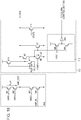
- Fig. 1A is a block diagram illustrating a configuration example of a photoelectric conversion apparatus according to a first embodiment.
- the photoelectric conversion apparatus includes a pixel array 102 having a plurality of pixels 100 arranged in a matrix form.
- a variable gain column amplification unit 103 and an analog memory 201 are provided for each column in the pixel array.
- a column comparison unit 105, a column control unit 106, and a digital memory 108 are provided for each of the column amplification units 103.
- the photoelectric conversion apparatus further includes a vertical scanning unit 101 configured to control the pixels 100 in rows, a reference signal generation unit 104 configured to generate a reference signal, and a horizontal scanning unit 109 configured to control the digital memory 108 and analog memory 201.
- the photoelectric conversion apparatus may further include an output buffer 202 configured to buffer and output a signal output from the analog memory 201.
- the column amplification unit 103, analog memory 201, column comparison unit 105, column control unit 106 and memory 108 will be collectively called a column signal processing unit.
- Each of the column amplification units 103 has an output node connected to input nodes of the corresponding column comparison unit 105 and analog memory 201.
- the column comparison unit 105 compares a signal output from the column amplification unit 103 and a reference signal supplied from the reference signal generation unit 104 and outputs the result as a comparison result signal to the column control unit 106.
- the column control unit 106 supplies the comparison result signal to the digital memory 108 and supplies a gain setting signal ATT to the column amplification unit 103 in accordance with the comparison result signal.
- the column amplification unit 103 has a gain which is set based on the gain setting signal ATT.
- the horizontal scanning unit 109 selects the digital memory 108 and analog memory 201 in each column, and signals held therein are output to a circuit in a following stage. It is assumed here that the following switches are turned on when a control signal has a high level and are turned off when a control signal has a low level.
- Fig. 1B is an equivalent circuit diagram illustrating a configuration example of each of the pixels 100.
- Each of the pixels 100 includes a photo diode PD which is a photoelectric conversion pixel, a transfer transistor TX, a reset transistor RES, an amplifying transistor SF, and a selection transistor SEL.
- the transfer transistor TX is turned on in response to a signal PTX, charges generated in the photo diode PD are transferred to a capacitance present in a gate node of the amplifying transistor SF.
- the node will be called a floating diffusion part FD.
- the amplifying transistor SF configures a source follower circuit along with a current source, not illustrated, and outputs a voltage signal based on the amount of electric charges held in the floating diffusion part FD.
- the current source is generally provided commonly to the plurality of pixels 100.
- the reset transistor RES is controlled with the signal PRES and discharges the charges held in the floating diffusion part FD to the power supply.
- Fig. 2 illustrates configuration examples of the column amplification unit 103, column comparison unit 105 and column control unit 106.
- the column amplification unit 103 has an input node VIN connected to an output OUT of the corresponding pixel 100 and the aforementioned current source.
- the column amplification unit 103 includes an input capacitance C0, an amplification unit amp, feedback capacitances Cf1 and Cf2, a switch Sf2, a column amplification unit reset switch Sr, and an OR circuit OR1.
- the amplification unit amp is a differential amplifier in this embodiment.
- the feedback capacitances Cf1 and Cf2 are provided between input and output nodes of the amplification unit amp which is an amplifier.
- the OR circuit OR1 outputs a signal corresponding to a logical sum of the signal ATT output from the column control unit 106 and a signal PCFR output from a timing control unit, not illustrated and switches on or off the switch Sf2.
- the switch Sr is switched on or off in accordance with a signal PC0R.
- the column amplification unit 103 has a gain depending on a ratio between a value of a capacitance connected to a feedback path of the amplification unit amp and a capacitance value of the input capacitance C0.
- the switch Sf2 has an ON state
- the column amplification unit 103 has a gain of - ⁇ C0/(Cf1 + Cf2) ⁇ .
- the column amplification unit has a gain of - (C0/Cf1).
- This embodiment assumes that the input capacitance C0 and feedback capacitances Cf1 and Cf2 have capacitance values C0, C0, 3*C0, respectively. In other words, when the switch Sf2 has an ON state, the gain is 1/4 times. When the switch Sf2 has an OFF state, the gain is 1 time.
- the switch Sf2 is provided between an inverting input terminal of the amplification unit amp and the feedback capacitance Cf2.
- the switch Sf2 may be provided in parallel with the feedback capacitance Cf1 and switch Sr in the path between the output terminal of the amplification unit amp and the feedback capacitance Cf2. Switches controlled by signals having an identical phase may be provided across the feedback capacitance Cf2.
- the column comparison unit 105 includes a comparator comp having input nodes both connected to capacitances. An output from the column amplification unit 103 is input to one input node of the comparator comp through the capacitance, and a reference signal VRMP is input to the other input node of the comparator comp through the other capacitance. A comparison result signal output from the comparator comp is supplied to the column control unit 106.
- Fig. 3 is a timing chart for explaining operations according to this embodiment.
- Fig. 3 illustrates signals to be supplied to each of the pixels 100 and signals associated with the column amplification unit 103, column comparison unit 105, and column control unit 106.
- Section (a) in Fig. 3 illustrates operations performed in a case when the signal VOUT output from the column amplification unit 103 is lower than a threshold
- Section (b) in Fig. 3 illustrates operations performed in a case where the signal VOUT output from the column amplification unit 103 is larger than the threshold.
- Section (a) corresponds to a case where light having lower intensity enters to a pixel from which a signal is read out (low luminance condition), for example
- Section (b) corresponds to a case where intense light enters to a pixel from which a signal is read out (high luminance condition), for example.
- the quantity of light incident on the pixel in the Section (b) case is higher than the quantity of light incident on the pixel in the Section (a) case.
- the selection transistor SEL When the signal PEEL has a high level at a time t1, the selection transistor SEL is turned on, and the amplifying transistor SF operates as a source follower circuit with a current source, not illustrated.
- the reset transistor RES When the signal PRES has a high level at the time t1, the reset transistor RES is turned on, and the potential of the floating diffusion part FD is reset.
- the switches Sr and Sf2 are turned on.
- a short circuit is established between the input and output nodes of the amplification unit amp, and a short circuit is established between both nodes of the feedback capacitance Cf2.
- both nodes of the feedback capacitances Cf1 and Cf2 are reset by the output of the amplification unit amp.
- the amplification unit amp operates as a voltage follower circuit.
- the signal PRES has a low level, and the reset transistor RES is turned off.
- a signal corresponding to the noise caused by the reset of the floating diffusion part FD is output from the pixel and appears at the input VIN of the column amplification unit.
- the signal PCFR has a low level, and the feedback capacitance Cf2 is electrically isolated from the feedback path of the amplification unit amp.
- the column amplification unit 103 has a gain of -(C0/Cf1).
- the reference signal VRMP changes to a threshold VTH.
- the output of the column amplification unit 103 is lower than the threshold VTH as in Section (a) in Fig. 3 , that is, when a low luminance signal is input to the column comparison unit 105, the signal ATT keeps a low level.
- the switch Sf2 keeps its OFF state.
- the column amplification unit 103 maintains a gain of -(C0/Cf).
- the threshold VTH may be a value corresponding to a saturation level of the output of the column amplification unit 103, for example, and a signal having a value larger than it may be determined as having the saturation level.
- the column control unit keeps the logic level of the signal ATT.
- the output VOUT from the column amplification unit 103 is held in the analog memory 201, and the signal ATT is held in the digital memory 108.
- the signal held in the analog memory 201 is read out, and the signal held in the digital memory 108 is read out.
- which gain is applied to amplify the signal read out from the analog memory 201 may be identified by a circuit in a following stage.
- a signal output from the pixel 100 may be amplified with an appropriate gain for a high S/N ratio and a wide dynamic range.
- the two feedback capacitances Cf1 and Cf2 both electrically connected to the feedback path of the amplification unit amp are reset, and one of them is then isolated from the feedback path.
- the feedback capacitance isolated from the feedback path is again electrically connected to the feedback path to reduce the gain of the column amplification unit 103.
- the noise superimposed on the signal may be reduced when the gain of the column amplification unit 103 is switched.
- the signal PCFR has a low level.
- the inverting input node of the amplification unit amp is reset by the output of the amplification unit amp, and the switch Sf2 is then turned off. Therefore, the noise caused by the switching off of the switch Sf2 is cancelled by the output of the amplification unit amp. In other words, with a gain of - (C0/Cf), the influence of the switching noise due to the switch Sf2 may be reduced.
- the switch Sf2 is turned on. Therefore, because charges of switching noise caused by the switching on of the switch Sf2 are divided to the two feedback capacitances Cf1 and Cf2, the influence of the switching noise may be reduced.
- the occurrence of an offset may be inhibited and at the same time a higher S/N ratio and a wide dynamic range may be acquired.
- Fig. 4 is an equivalent circuit diagram illustrating another configuration example of the column amplification unit 103. It is different from the configuration example of the column amplification unit 103 illustrated in Fig. 2 in that more feedback capacitances are provided than that of the configuration illustrated in Fig. 2 and that different capacitance values of the input capacitance and feedback capacitances are applied. According to this embodiment, six feedback capacitances are provided which have capacitance values of C, C, 2 ⁇ C, 4 ⁇ C, 8 ⁇ C, and 16 ⁇ C, respectively. The input capacitance has a capacitance value of 8 ⁇ C.
- the configuration of this embodiment allows switching between three or more kinds of gain by changing the combination of the switches s0 to s4 to be brought into conduction.
- the column amplification unit 103 is a programmable gain amplifier for which four kinds of setting are possible with a 2-bit signal r_gain.
- the signal ATT has an L level, it means that a low luminance signal has been input to the column amplification unit 103.
- the signal ATT has an H level, it means that a high luminance signal has been input to the column amplification unit 103.
- Fig. 5 illustrates settings in cases where the signal ATT has an L level and where the signal STT has an H level.
- Fig. 5 illustrates signals r_gain with different states of the signal ATT and states of the switches s0 to s4.
- the switches s0 and s1 are turned on, and the switches s2 to s4 are turned off.
- the gain of the column amplification unit 103 is two times.
- Fig. 5 illustrates an example in which four gains of one time, two times, four times and eight times are settable for the column amplification unit 103 in response to a low luminance signal, and four gains of 1/4 times, 1/2 times, one time, and two times are settable for the column amplification unit 103 in response to a high luminance signal.
- the switches s0 to s4 may be controlled with one of the settings 00 to 11 of the signal r_gain as on the table illustrated in Fig. 5 so that the gain ratio between a case where the signal ATT has an L level and a case where the signal ATT has an H level may be kept at 1:1/4.
- the signal r_gain for determining a programmable gain may be changed in accordance with luminance information of an imaging scene or the value of ISO sensitivity set by an imaging system, for example.
- individual controls over the switches s0 to s4 are allowed in accordance with the output of the column control unit 106, and at least a high level of one of the outputs of the column control unit 106 or the signal PCFR may turn on the corresponding switch.
- a high S/N ratio and a dynamic range may be acquired like the first embodiment, and switching between more gains may be allowed.
- more detail switching between gains of the column amplification unit 103 may be allowed in accordance with signal levels advantageously.
- Fig. 6 is a block diagram illustrating a configuration of an imaging apparatus according to a third embodiment.
- the imaging apparatus according to this embodiment is different from the imaging apparatus illustrated in Figs. 1A and 1B in that a reference signal generation unit 104, a column comparison unit 105, and a column counter unit 107 are used to perform an analog-digital conversion (hereinafter, called AD conversion) on a signal output from the column amplification unit 103.
- AD conversion analog-digital conversion
- this embodiment is different from the aforementioned embodiments in that a column signal processing unit CP includes an AD converter.
- a signal output from the column amplification unit 103 is compared in the column comparison unit 105 with a reference signal VRMP output from the reference signal generation unit 104.
- the reference signal VRMP is changed monotonously with time, and the column counter unit 107 is caused to perform a counting operation.
- counted values changed until the magnitude relationship between the output from the column amplification unit 103 and the reference signal VRMP is inverted are digital signals corresponding to the signal output from the column amplification unit 103.
- the digital memory 108 holds the counted values of the column counter unit 107. When the digital memories 108 in columns are selected by the horizontal scanning unit 109, the counted values held by them are output to a node DOUT.
- Fig. 7 illustrates other configuration examples of the column amplification unit 103, column comparison unit 105 and column control unit 106. Differences from the circuit diagram in Fig. 2 will be described mainly.
- the column amplification unit 103 according to this embodiment is different from the column amplification unit 103 illustrated in Fig. 2 in that the amplification unit amp is not a differential amplifier.
- the column comparison unit 105 includes a column output limiting unit 110.
- the column output limiting unit 110 includes a clipping circuit which controls the output VOUT from the column amplification unit 103 so as to have a potential based on a clip voltage VCLP below a predetermined potential.
- the column control unit 106 changes the gain of the column amplification unit 103 to a lower gain by using the signal ATT, according to this embodiment.
- the column output limiting unit 110 operates to switch the signal ATT in accordance with the determination result on whether the output VOUT is being limited by the column output limiting unit 110 or not.
- Fig. 8 is a timing chart for explaining operations according to this embodiment. The operations will be described with reference to Figs. 6 to 8 .
- Fig. 8 illustrates in Section (a) an output from the column amplification unit 103, the reference signal VRMP, and the signal ATT in a case where the signal output from the column amplification unit 103 is a low luminance signal.
- Section (b) on the other hand illustrates an output from the column amplification unit 103, the reference signal VRMP, and the signal ATT in a case where the signal output from the column amplification unit 103 is a high luminance signal.
- the references (a) and (b) are not given to parts common in both of Sections (a) and (b).
- the reference signal generation unit 104 monotonically increases the reference signal VRMP from an initial value with time. If the reference signal VRMP is larger than the output VOUT from the column amplification unit 103 at a certain time, the logic level of the output from the column comparison unit 105 is inverted. In response thereto, the counting operation performed by the column counter unit 107 stops. Thus, a signal containing noise due to the reset of the column amplification unit 103 is AD converted (N_AD in Fig. 8 ). After the counting operation stops, the counted value is transferred to the digital memory 108.
- the column control unit 106 changes the signal ATT to a high level. Because this turns on the switch Sf2, the gain of the column amplification unit 103 decreases from 1 time to 1/4 times.
- the reference signal generation unit 104 at a time t14 monotonously increases the reference signal VRMP with time.
- the slope with time of the reference signal VRMP may be equal to that in the period from the time t10 to the time t11.
- the logic level of the output of the column comparison unit 105 is inverted.
- the counting operation of the column counter unit 107 stops.
- an optical signal based on the charges generated in a photoelectric conversion unit is AD converted (S_AD in Fig. 8 ).
- the counted value is transferred to the digital memory 108.
- a signal processing unit may be used to acquire a difference between a digital signal acquired by the operation performed during the period from the time t10 to the time t11 and a digital signal acquired by the operation performed during the period from the time t14 to the time t15 to perform a CDS process so that noise due to the reset of the column amplification unit 103 may be reduced.
- the column control unit 106 stores an identification signal describing whether the column output limiting unit 110 has limited the output from the column amplification unit 103 or not in the digital memory 108. A circuit in a following stage is allowed to determine from the identification signal which gain setting is applied in the column amplification unit 103 to acquire the digital signal.
- the feedback capacitance Cf2 is isolated from the feedback path of the amplifier amp. After that, when the output of the column amplification unit 103 is limited by the column output limiting unit 110, the feedback capacitance Cf2 is again connected to the feedback path of the amplifier amp. Thus, the charges due to switching noise caused by the switching on of the switch Sf2 are divided into the two feedback capacitances Cf1 and Cf2. Therefore, the influence of the switching noise may be reduced.
- the column amplification unit 103 may be used.
- Fig. 9 is an equivalent circuit diagram illustrating more detail configurations of the amplification unit amp and the column output limiting unit 110.
- the amplification unit amp is a common-source amplification circuit including four transistors M1 to M4.
- the NMOS transistor M4 is an amplifying transistor in the common-source amplification circuit and has a gate receiving a signal to be amplified by the amplification unit amp.
- the NMOS transistor M3 is a common-gate transistor serially connected to the NMOS transistor M4.
- the PMOS transistors M1 and M2 are cascade-connected constant current loads. In this embodiment, 4 ⁇ A current may be supplied.
- Voltages VBPB, VBPG, and VBNG to be fed to gates of the PMOS transistors M1 and M2 and the NMOS transistor M3 are bias voltages for determining operation points of the corresponding transistors.
- the column output limiting unit 110 includes transistors M5 to M7.
- the PMOS transistor M5 functions as a clip transistor.
- the PMOS transistor M5 has a source connected to the output node VOUT, a drain connected to a GND through the NMOS transistor M6 and connected to a gate of the NMOS transistor M7 and a judgment value output unit 112.
- a clip voltage VCLP is fed to the gate of the PMOS transistor M5.
- the NMOS transistor M6 is a transistor functioning as a load for sinking constant current when the PMOS transistor M5 is turned on, and its operation point is determined in accordance with a bias voltage VBNB. According to this embodiment, the NMOS transistor M6 is capable of supplying 1 ⁇ A current.
- the NMOS transistor M7 has a drain connected to the output node VOUT and a source connected to the GND.
- the judgment value output unit 112 includes a 2-stage inverter circuit. A signal output from the judgment value output unit 112 is input to the column control unit 106.
- the column output limiting unit 110 When the output of the amplification unit amp has a sufficiently low level, the PMOS transistor M5 has an OFF state. In this case, because the NMOS transistor M6 has an ON state, the NMOS transistor M7 has a gate voltage substantially equal to a GND level. Therefore, the NMOS transistor M7 also has an OFF state. As a result, because the PMOS transistor M5 and NMOS transistor M7 both have an OFF state, the column output limiting unit 110 does not substantially have an influence on the output from the amplification unit amp.
- the source voltage of the PMOS transistor M5 that is, the voltage of the output node VOUT is larger than a threshold depending on the clip voltage VCLP
- the PMOS transistor M5 is changed to have an ON state.
- the gate voltage of the NMOS transistor M7 rises, and the NMOS transistor M7 is also changed to have an ON state.
- the judgment value output unit 112 includes a 2-stage inverter and outputs a signal indicating that the gate voltage of the NMOS transistor M7 has increased. In other words, this signal indicates that the output limitation performed by the PMOS transistor M5 is active.
- the column control unit 106 having received the signal transmits a signal indicating that a clip operation has been performed, that is, the output of the amplification unit amp has been limited to a circuit in a following stage.
- Fig. 10 illustrates another configuration example of the output limiting unit.
- two clip voltages which are threshold values for performing the output limitation operation by the amplification unit amp are settable.
- the first clip voltage VCLP to be fed to the PMOS transistor M5 which is a first clip transistor and the second clip voltage VCLP2 to be fed to a PMOS transistor M12 which is a second clip transistor have a relationship of VCLP ⁇ VCLP2.
- the column output limiting unit 110 illustrated in Fig. 10 includes the transistors M5 to M12.
- the PMOS transistor M5 has a source connected to the output node VOUT and a drain connected to the GND through the NMOS transistor M6 and to gates of the NMOS transistor M7 and NMOS transistor M9.
- the PMOS transistor M5 has a gate connected to the output of an inverter circuit including the PMOS transistor M10 and NMOS transistor M11.
- the inverter circuit including the PMOS transistor M10 and NMOS transistor M11 supplies the clip voltage VCLP or vdd to the gate of the PMOS transistor M5 in accordance with a signal PCLP_EN.
- the NMOS transistor M6 is a transistor functioning as a load which sinks constant current when the PMOS transistor M5 is turned on, and its operation point is determined in accordance with the bias voltage VBNB. According to this embodiment, the NMOS transistor M6 is capable of supplying 1 ⁇ A current.
- the NMOS transistor M7 has a drain connected to the output node VOUT and a source connected to the GND.
- the PMOS transistor M8 and NMOS transistor M9 correspond to the inverter circuit in the first stage of the 2-stage inverter circuit in Fig. 9 .
- Fig. 11 is a timing chart for explaining operations to be performed when the circuit illustrated in Fig. 10 is used.
- Fig. 11 is the same as Fig. 8 except that signals PJDG and PCLP_EN are added. Therefore, the description on the same operations as those in Fig. 8 will be omitted properly.
- the signal PCLP_EN is changed to have a high level at a time t16 after the time t4 when the reset of the column amplification unit 103 completes.
- the PMOS transistor M5 is turned to have the gate voltage VCLP.
- both of the PMOS transistors M5 and M12 may function as clip transistors.
- the PMOS transistor M5 is activated based on the relationship VCLP2 > VCLP.
- the signal PJDG is changed to have a high level from a time t17.
- the output from the inverter circuit including the PMOS transistor M8 and NMOS transistor M9 has a high impedance state.
- the output from the inverter circuit is held at a high level by parasitic capacitance existing.
- the PMOS transistor M5 When a high luminance signal is input to the column amplification unit 103 from the time t12, the PMOS transistor M5 is turned on. Thus, the gate voltages of the NMOS transistors M7 and M9 increase, and the output from the inverter including the transistors M8 and M9 is inverted to a low level. Based on the signal, the column control unit 106 shifts the signal ATT to a high level. Then, the signals PCLP_EN and PJDGAD are shifted to a low level at a time t18 before the time t14 when a conversion is started. Thus, the PMOS transistor M5 and the judgment value output unit 112 are shifted to a non-operational state, and the PMOS transistor M12 is only activated.
- the clip voltage VCLP is fed to the gate of the PMOS transistor M5 and the voltage of the output node VOUT is slightly lower than a threshold voltage depending on the clip voltage VCLP, the PMOS transistor M5 may operate in a sub-threshold region.
- the amplification unit amp may not possibly output a proper value. Accordingly, the processing as described above may securely shift the PMOS transistor M5 to an OFF state.
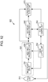
- FIG. 12 illustrates a configuration example of an imaging system.
- An imaging system 800 may include, for example, optical unit 810, an image pickup device 100, a video signal processing unit 830, a recording/communication unit 840, a timing control unit 850, a system control unit 860, and a reproduction/display unit 870.
- the imaging apparatus 820 has the image pickup device 100 and the video signal processing unit 830.
- the image pickup device 100 may be a photoelectric conversion apparatus according to one of the aforementioned embodiments.
- the optical unit 810 which is an optical system such as a lens focuses light from a photographic subject to form an image of the photographic subject in a pixel part 10 including a plurality of pixels arranged two-dimensionally in the image pickup device 100.
- the image pickup device 100 outputs a signal according to the light imaged in the pixel part 10 at a time point based on the signal from the timing control unit 850.
- the signal output from the image pickup device 100 is input to the video signal processing unit 830 which is a video signal processing unit, and the video signal processing unit 830 performs a signal process according to a method defined in a program, for example.
- the signal acquired by the process performed by the video signal processing unit 830 is transmitted to the recording/communication unit 840 as image data.
- the recording/communication unit 840 transmits the signal for forming an image to the reproduction/display unit 870 and causes the reproduction/display unit 870 to reproduce and display the corresponding moving image or a still image.
- the recording/communication unit 840 receives the signal from the video signal processing unit 830 and communicates with the system control unit 860 and performs an operation for recording a signal for forming an image in a recording medium, not illustrated.
- the system control unit 860 is configured to generally control operations performed by the imaging system optical unit 810 and controls driving of the timing control unit 850, recording/communication unit 840, and reproduction/display unit 870.
- the system control unit 860 may include a storage device, not illustrated, which is a recording medium, for example, and a program for controlling an operation performed by the imaging system is stored in the storage device.
- the system control unit 860 may supply a signal for switching the drive mode or sensitivity in accordance with a user operation, for example. Specific examples thereof may include a change of the row to be read out or be reset, a change of the field angle for electronic zooming, and a movement of a field angle for electronic vibration-proof.
- the system control unit 860 functions as a sensitivity selection unit for selecting the sensitivity of the imaging system 800, and the sensitivity of the image pickup device 100 is also switched in accordance with the selected sensitivity.
- the timing control unit 850 is configured to control driving timing of the image pickup device 100 and video signal processing unit 830 under control performed by the system control unit 860.
- the timing control unit 850 may also function as a sensitivity setting unit configured to set the imaging sensitivity of the image pickup device 100.
- an offset error caused when the gain of an amplification unit is switched may be reduced.
Landscapes
- Engineering & Computer Science (AREA)
- Multimedia (AREA)
- Signal Processing (AREA)
- Theoretical Computer Science (AREA)
- Transforming Light Signals Into Electric Signals (AREA)
- Solid State Image Pick-Up Elements (AREA)
- Computer Vision & Pattern Recognition (AREA)
Applications Claiming Priority (1)
| Application Number | Priority Date | Filing Date | Title |
|---|---|---|---|
| JP2014158961A JP6385190B2 (ja) | 2014-08-04 | 2014-08-04 | 光電変換装置の駆動方法、光電変換装置、および撮像システム |
Publications (2)
| Publication Number | Publication Date |
|---|---|
| EP2983353A1 EP2983353A1 (en) | 2016-02-10 |
| EP2983353B1 true EP2983353B1 (en) | 2018-03-14 |
Family
ID=53785436
Family Applications (1)
| Application Number | Title | Priority Date | Filing Date |
|---|---|---|---|
| EP15177061.7A Active EP2983353B1 (en) | 2014-08-04 | 2015-07-16 | Driving method for photoelectric conversion apparatus, photoelectric conversion apparatus, and imaging system |
Country Status (4)
| Country | Link |
|---|---|
| US (1) | US9774808B2 (enExample) |
| EP (1) | EP2983353B1 (enExample) |
| JP (1) | JP6385190B2 (enExample) |
| CN (1) | CN105338265B (enExample) |
Families Citing this family (4)
| Publication number | Priority date | Publication date | Assignee | Title |
|---|---|---|---|---|
| CN113382188B (zh) * | 2016-04-15 | 2024-08-16 | 索尼公司 | 光检测装置 |
| US10261626B2 (en) * | 2017-06-13 | 2019-04-16 | Synaptics Incorporated | Mitigating audible noise in a display having an integrated touch sensor |
| JP2019068267A (ja) * | 2017-09-29 | 2019-04-25 | キヤノン株式会社 | 撮像装置、撮像システム、移動体 |
| JP7706916B2 (ja) * | 2021-04-01 | 2025-07-14 | キヤノン株式会社 | 光電変換装置 |
Citations (1)
| Publication number | Priority date | Publication date | Assignee | Title |
|---|---|---|---|---|
| EP1538827A1 (en) * | 2003-12-05 | 2005-06-08 | Sony Corporation | Column readout circuit with increased signal range for CMOS image sensor |
Family Cites Families (15)
| Publication number | Priority date | Publication date | Assignee | Title |
|---|---|---|---|---|
| JP3844699B2 (ja) * | 2001-02-19 | 2006-11-15 | イノテック株式会社 | 可変利得アンプ |
| JP3872333B2 (ja) | 2001-12-07 | 2007-01-24 | 浜松ホトニクス株式会社 | 物体表面形状計測装置 |
| US7002408B2 (en) * | 2003-10-15 | 2006-02-21 | Varian Medical Systems Technologies, Inc. | Data signal amplifier and processor with multiple signal gains for increased dynamic signal range |
| JP4804254B2 (ja) * | 2006-07-26 | 2011-11-02 | キヤノン株式会社 | 光電変換装置及び撮像装置 |
| US7755017B2 (en) * | 2006-10-13 | 2010-07-13 | Sony Corporation | Solid-image-pickup device, image-pickup device, and method of driving solid-image-pickup device |
| JP5089528B2 (ja) * | 2008-08-18 | 2012-12-05 | パナソニック株式会社 | データ取り込み回路および表示パネル駆動回路および画像表示装置 |
| US8913166B2 (en) * | 2009-01-21 | 2014-12-16 | Canon Kabushiki Kaisha | Solid-state imaging apparatus |
| US8717474B2 (en) * | 2009-12-04 | 2014-05-06 | Canon Kabushiki Kaisha | Imaging apparatus and method for driving the same |
| JP2011259305A (ja) * | 2010-06-10 | 2011-12-22 | Toshiba Corp | 固体撮像装置 |
| JP5115601B2 (ja) * | 2010-08-06 | 2013-01-09 | ソニー株式会社 | 半導体装置およびその制御方法 |
| JP5429207B2 (ja) * | 2010-09-08 | 2014-02-26 | 株式会社デンソー | 容量式物理量検出装置 |
| CN103119928B (zh) * | 2010-09-30 | 2016-05-25 | 佳能株式会社 | 固态成像装置 |
| JP5935286B2 (ja) * | 2011-10-19 | 2016-06-15 | ソニー株式会社 | 撮像装置および撮像表示システム |
| JP5840947B2 (ja) * | 2011-12-27 | 2016-01-06 | 富士フイルム株式会社 | 放射線画像検出装置およびその駆動方法 |
| JP6164846B2 (ja) * | 2012-03-01 | 2017-07-19 | キヤノン株式会社 | 撮像装置、撮像システム、撮像装置の駆動方法 |
-
2014
- 2014-08-04 JP JP2014158961A patent/JP6385190B2/ja active Active
-
2015
- 2015-07-16 EP EP15177061.7A patent/EP2983353B1/en active Active
- 2015-07-31 US US14/815,759 patent/US9774808B2/en not_active Expired - Fee Related
- 2015-08-04 CN CN201510484665.9A patent/CN105338265B/zh active Active
Patent Citations (1)
| Publication number | Priority date | Publication date | Assignee | Title |
|---|---|---|---|---|
| EP1538827A1 (en) * | 2003-12-05 | 2005-06-08 | Sony Corporation | Column readout circuit with increased signal range for CMOS image sensor |
Also Published As
| Publication number | Publication date |
|---|---|
| JP2016036112A (ja) | 2016-03-17 |
| CN105338265B (zh) | 2018-07-03 |
| CN105338265A (zh) | 2016-02-17 |
| JP6385190B2 (ja) | 2018-09-05 |
| EP2983353A1 (en) | 2016-02-10 |
| US20160037091A1 (en) | 2016-02-04 |
| US9774808B2 (en) | 2017-09-26 |
Similar Documents
| Publication | Publication Date | Title |
|---|---|---|
| JP5858695B2 (ja) | 固体撮像装置及び固体撮像装置の駆動方法 | |
| US9445029B2 (en) | Solid-state imaging apparatus with plural column circuits arranged separately in upper and lower positions and driving method therefor | |
| US9402043B2 (en) | Method and systems for amplifying an output of a CMOS pixel array | |
| JP6319946B2 (ja) | 固体撮像装置及び撮像システム | |
| JP6736906B2 (ja) | 固体撮像装置及び画像読み取り装置 | |
| US8068155B2 (en) | Solid-state image sensor and driving method thereof, and image sensor | |
| US9787927B2 (en) | Solid-state imaging apparatus | |
| EP2360912B1 (en) | Solid-state image pickup apparatus and driving method therefor | |
| JP6463000B2 (ja) | 固体撮像装置及び撮像システム | |
| CN108989712B (zh) | 摄像装置 | |
| US9838637B2 (en) | Solid-state image sensor, method of controlling the same, image sensing system, and camera | |
| JP2011004390A (ja) | 撮像装置、撮像システム、及び撮像装置の駆動方法 | |
| JP2014222863A (ja) | 撮像装置 | |
| US10811448B2 (en) | Solid-state imaging device | |
| US9800810B2 (en) | Imaging apparatus and imaging system | |
| EP2983353B1 (en) | Driving method for photoelectric conversion apparatus, photoelectric conversion apparatus, and imaging system | |
| CN113728620A (zh) | 差量视觉传感器 | |
| US10104321B1 (en) | Image processing system and method for an image sensor | |
| US20230164456A1 (en) | Analog-to-digital converting circuit for optimizing dual conversion gain operation and operation method thereof | |
| US9825082B2 (en) | Pixel amplification apparatus, CMOS image sensor including the same and operation method thereof | |
| JP4650445B2 (ja) | クランプ信号生成装置およびクランプ信号生成方法 | |
| US9807333B2 (en) | Imaging apparatus and imaging system |
Legal Events
| Date | Code | Title | Description |
|---|---|---|---|
| PUAI | Public reference made under article 153(3) epc to a published international application that has entered the european phase |
Free format text: ORIGINAL CODE: 0009012 |
|
| AK | Designated contracting states |
Kind code of ref document: A1 Designated state(s): AL AT BE BG CH CY CZ DE DK EE ES FI FR GB GR HR HU IE IS IT LI LT LU LV MC MK MT NL NO PL PT RO RS SE SI SK SM TR |
|
| AX | Request for extension of the european patent |
Extension state: BA ME |
|
| 17P | Request for examination filed |
Effective date: 20160810 |
|
| RBV | Designated contracting states (corrected) |
Designated state(s): AL AT BE BG CH CY CZ DE DK EE ES FI FR GB GR HR HU IE IS IT LI LT LU LV MC MK MT NL NO PL PT RO RS SE SI SK SM TR |
|
| 17Q | First examination report despatched |
Effective date: 20170203 |
|
| REG | Reference to a national code |
Ref country code: DE Ref legal event code: R079 Ref document number: 602015008667 Country of ref document: DE Free format text: PREVIOUS MAIN CLASS: H04N0005378000 Ipc: H03M0001180000 |
|
| RIC1 | Information provided on ipc code assigned before grant |
Ipc: H04N 5/335 20110101ALI20170803BHEP Ipc: H04N 5/355 20110101ALI20170803BHEP Ipc: H04N 5/378 20110101ALI20170803BHEP Ipc: H03M 1/56 20060101ALI20170803BHEP Ipc: H04N 3/14 20060101ALI20170803BHEP Ipc: H04N 5/374 20110101ALI20170803BHEP Ipc: H04N 5/243 20060101ALI20170803BHEP Ipc: H03M 1/18 20060101AFI20170803BHEP Ipc: H04N 5/3745 20110101ALI20170803BHEP |
|
| GRAP | Despatch of communication of intention to grant a patent |
Free format text: ORIGINAL CODE: EPIDOSNIGR1 |
|
| RIN1 | Information on inventor provided before grant (corrected) |
Inventor name: HASHIMOTO, SEIJI Inventor name: YOSHIDA, DAISUKE |
|
| RAP1 | Party data changed (applicant data changed or rights of an application transferred) |
Owner name: CANON KABUSHIKI KAISHA |
|
| INTG | Intention to grant announced |
Effective date: 20170926 |
|
| GRAS | Grant fee paid |
Free format text: ORIGINAL CODE: EPIDOSNIGR3 |
|
| GRAA | (expected) grant |
Free format text: ORIGINAL CODE: 0009210 |
|
| AK | Designated contracting states |
Kind code of ref document: B1 Designated state(s): AL AT BE BG CH CY CZ DE DK EE ES FI FR GB GR HR HU IE IS IT LI LT LU LV MC MK MT NL NO PL PT RO RS SE SI SK SM TR |
|
| REG | Reference to a national code |
Ref country code: GB Ref legal event code: FG4D |
|
| REG | Reference to a national code |
Ref country code: CH Ref legal event code: EP Ref country code: AT Ref legal event code: REF Ref document number: 979788 Country of ref document: AT Kind code of ref document: T Effective date: 20180315 |
|
| REG | Reference to a national code |
Ref country code: IE Ref legal event code: FG4D |
|
| REG | Reference to a national code |
Ref country code: DE Ref legal event code: R096 Ref document number: 602015008667 Country of ref document: DE |
|
| REG | Reference to a national code |
Ref country code: NL Ref legal event code: MP Effective date: 20180314 |
|
| REG | Reference to a national code |
Ref country code: LT Ref legal event code: MG4D |
|
| PG25 | Lapsed in a contracting state [announced via postgrant information from national office to epo] |
Ref country code: HR Free format text: LAPSE BECAUSE OF FAILURE TO SUBMIT A TRANSLATION OF THE DESCRIPTION OR TO PAY THE FEE WITHIN THE PRESCRIBED TIME-LIMIT Effective date: 20180314 Ref country code: CY Free format text: LAPSE BECAUSE OF FAILURE TO SUBMIT A TRANSLATION OF THE DESCRIPTION OR TO PAY THE FEE WITHIN THE PRESCRIBED TIME-LIMIT Effective date: 20180314 Ref country code: LT Free format text: LAPSE BECAUSE OF FAILURE TO SUBMIT A TRANSLATION OF THE DESCRIPTION OR TO PAY THE FEE WITHIN THE PRESCRIBED TIME-LIMIT Effective date: 20180314 Ref country code: FI Free format text: LAPSE BECAUSE OF FAILURE TO SUBMIT A TRANSLATION OF THE DESCRIPTION OR TO PAY THE FEE WITHIN THE PRESCRIBED TIME-LIMIT Effective date: 20180314 Ref country code: NO Free format text: LAPSE BECAUSE OF FAILURE TO SUBMIT A TRANSLATION OF THE DESCRIPTION OR TO PAY THE FEE WITHIN THE PRESCRIBED TIME-LIMIT Effective date: 20180614 |
|
| REG | Reference to a national code |
Ref country code: AT Ref legal event code: MK05 Ref document number: 979788 Country of ref document: AT Kind code of ref document: T Effective date: 20180314 |
|
| PG25 | Lapsed in a contracting state [announced via postgrant information from national office to epo] |
Ref country code: GR Free format text: LAPSE BECAUSE OF FAILURE TO SUBMIT A TRANSLATION OF THE DESCRIPTION OR TO PAY THE FEE WITHIN THE PRESCRIBED TIME-LIMIT Effective date: 20180615 Ref country code: RS Free format text: LAPSE BECAUSE OF FAILURE TO SUBMIT A TRANSLATION OF THE DESCRIPTION OR TO PAY THE FEE WITHIN THE PRESCRIBED TIME-LIMIT Effective date: 20180314 Ref country code: SE Free format text: LAPSE BECAUSE OF FAILURE TO SUBMIT A TRANSLATION OF THE DESCRIPTION OR TO PAY THE FEE WITHIN THE PRESCRIBED TIME-LIMIT Effective date: 20180314 Ref country code: LV Free format text: LAPSE BECAUSE OF FAILURE TO SUBMIT A TRANSLATION OF THE DESCRIPTION OR TO PAY THE FEE WITHIN THE PRESCRIBED TIME-LIMIT Effective date: 20180314 Ref country code: BG Free format text: LAPSE BECAUSE OF FAILURE TO SUBMIT A TRANSLATION OF THE DESCRIPTION OR TO PAY THE FEE WITHIN THE PRESCRIBED TIME-LIMIT Effective date: 20180614 |
|
| PG25 | Lapsed in a contracting state [announced via postgrant information from national office to epo] |
Ref country code: IT Free format text: LAPSE BECAUSE OF FAILURE TO SUBMIT A TRANSLATION OF THE DESCRIPTION OR TO PAY THE FEE WITHIN THE PRESCRIBED TIME-LIMIT Effective date: 20180314 Ref country code: AL Free format text: LAPSE BECAUSE OF FAILURE TO SUBMIT A TRANSLATION OF THE DESCRIPTION OR TO PAY THE FEE WITHIN THE PRESCRIBED TIME-LIMIT Effective date: 20180314 Ref country code: ES Free format text: LAPSE BECAUSE OF FAILURE TO SUBMIT A TRANSLATION OF THE DESCRIPTION OR TO PAY THE FEE WITHIN THE PRESCRIBED TIME-LIMIT Effective date: 20180314 Ref country code: PL Free format text: LAPSE BECAUSE OF FAILURE TO SUBMIT A TRANSLATION OF THE DESCRIPTION OR TO PAY THE FEE WITHIN THE PRESCRIBED TIME-LIMIT Effective date: 20180314 Ref country code: EE Free format text: LAPSE BECAUSE OF FAILURE TO SUBMIT A TRANSLATION OF THE DESCRIPTION OR TO PAY THE FEE WITHIN THE PRESCRIBED TIME-LIMIT Effective date: 20180314 Ref country code: NL Free format text: LAPSE BECAUSE OF FAILURE TO SUBMIT A TRANSLATION OF THE DESCRIPTION OR TO PAY THE FEE WITHIN THE PRESCRIBED TIME-LIMIT Effective date: 20180314 Ref country code: RO Free format text: LAPSE BECAUSE OF FAILURE TO SUBMIT A TRANSLATION OF THE DESCRIPTION OR TO PAY THE FEE WITHIN THE PRESCRIBED TIME-LIMIT Effective date: 20180314 |
|
| PG25 | Lapsed in a contracting state [announced via postgrant information from national office to epo] |
Ref country code: AT Free format text: LAPSE BECAUSE OF FAILURE TO SUBMIT A TRANSLATION OF THE DESCRIPTION OR TO PAY THE FEE WITHIN THE PRESCRIBED TIME-LIMIT Effective date: 20180314 Ref country code: CZ Free format text: LAPSE BECAUSE OF FAILURE TO SUBMIT A TRANSLATION OF THE DESCRIPTION OR TO PAY THE FEE WITHIN THE PRESCRIBED TIME-LIMIT Effective date: 20180314 Ref country code: SK Free format text: LAPSE BECAUSE OF FAILURE TO SUBMIT A TRANSLATION OF THE DESCRIPTION OR TO PAY THE FEE WITHIN THE PRESCRIBED TIME-LIMIT Effective date: 20180314 Ref country code: SM Free format text: LAPSE BECAUSE OF FAILURE TO SUBMIT A TRANSLATION OF THE DESCRIPTION OR TO PAY THE FEE WITHIN THE PRESCRIBED TIME-LIMIT Effective date: 20180314 |
|
| REG | Reference to a national code |
Ref country code: DE Ref legal event code: R097 Ref document number: 602015008667 Country of ref document: DE |
|
| PG25 | Lapsed in a contracting state [announced via postgrant information from national office to epo] |
Ref country code: PT Free format text: LAPSE BECAUSE OF FAILURE TO SUBMIT A TRANSLATION OF THE DESCRIPTION OR TO PAY THE FEE WITHIN THE PRESCRIBED TIME-LIMIT Effective date: 20180716 |
|
| PLBE | No opposition filed within time limit |
Free format text: ORIGINAL CODE: 0009261 |
|
| STAA | Information on the status of an ep patent application or granted ep patent |
Free format text: STATUS: NO OPPOSITION FILED WITHIN TIME LIMIT |
|
| PG25 | Lapsed in a contracting state [announced via postgrant information from national office to epo] |
Ref country code: DK Free format text: LAPSE BECAUSE OF FAILURE TO SUBMIT A TRANSLATION OF THE DESCRIPTION OR TO PAY THE FEE WITHIN THE PRESCRIBED TIME-LIMIT Effective date: 20180314 |
|
| 26N | No opposition filed |
Effective date: 20181217 |
|
| PG25 | Lapsed in a contracting state [announced via postgrant information from national office to epo] |
Ref country code: SI Free format text: LAPSE BECAUSE OF FAILURE TO SUBMIT A TRANSLATION OF THE DESCRIPTION OR TO PAY THE FEE WITHIN THE PRESCRIBED TIME-LIMIT Effective date: 20180314 |
|
| REG | Reference to a national code |
Ref country code: CH Ref legal event code: PL |
|
| PG25 | Lapsed in a contracting state [announced via postgrant information from national office to epo] |
Ref country code: LU Free format text: LAPSE BECAUSE OF NON-PAYMENT OF DUE FEES Effective date: 20180716 Ref country code: MC Free format text: LAPSE BECAUSE OF FAILURE TO SUBMIT A TRANSLATION OF THE DESCRIPTION OR TO PAY THE FEE WITHIN THE PRESCRIBED TIME-LIMIT Effective date: 20180314 |
|
| REG | Reference to a national code |
Ref country code: BE Ref legal event code: MM Effective date: 20180731 |
|
| REG | Reference to a national code |
Ref country code: IE Ref legal event code: MM4A |
|
| PG25 | Lapsed in a contracting state [announced via postgrant information from national office to epo] |
Ref country code: IE Free format text: LAPSE BECAUSE OF NON-PAYMENT OF DUE FEES Effective date: 20180716 Ref country code: FR Free format text: LAPSE BECAUSE OF NON-PAYMENT OF DUE FEES Effective date: 20180731 Ref country code: LI Free format text: LAPSE BECAUSE OF NON-PAYMENT OF DUE FEES Effective date: 20180731 Ref country code: CH Free format text: LAPSE BECAUSE OF NON-PAYMENT OF DUE FEES Effective date: 20180731 |
|
| PG25 | Lapsed in a contracting state [announced via postgrant information from national office to epo] |
Ref country code: BE Free format text: LAPSE BECAUSE OF NON-PAYMENT OF DUE FEES Effective date: 20180731 |
|
| PG25 | Lapsed in a contracting state [announced via postgrant information from national office to epo] |
Ref country code: MT Free format text: LAPSE BECAUSE OF NON-PAYMENT OF DUE FEES Effective date: 20180716 |
|
| GBPC | Gb: european patent ceased through non-payment of renewal fee |
Effective date: 20190716 |
|
| PG25 | Lapsed in a contracting state [announced via postgrant information from national office to epo] |
Ref country code: TR Free format text: LAPSE BECAUSE OF FAILURE TO SUBMIT A TRANSLATION OF THE DESCRIPTION OR TO PAY THE FEE WITHIN THE PRESCRIBED TIME-LIMIT Effective date: 20180314 |
|
| PG25 | Lapsed in a contracting state [announced via postgrant information from national office to epo] |
Ref country code: GB Free format text: LAPSE BECAUSE OF NON-PAYMENT OF DUE FEES Effective date: 20190716 |
|
| PG25 | Lapsed in a contracting state [announced via postgrant information from national office to epo] |
Ref country code: MK Free format text: LAPSE BECAUSE OF NON-PAYMENT OF DUE FEES Effective date: 20180314 Ref country code: HU Free format text: LAPSE BECAUSE OF FAILURE TO SUBMIT A TRANSLATION OF THE DESCRIPTION OR TO PAY THE FEE WITHIN THE PRESCRIBED TIME-LIMIT; INVALID AB INITIO Effective date: 20150716 |
|
| PG25 | Lapsed in a contracting state [announced via postgrant information from national office to epo] |
Ref country code: IS Free format text: LAPSE BECAUSE OF FAILURE TO SUBMIT A TRANSLATION OF THE DESCRIPTION OR TO PAY THE FEE WITHIN THE PRESCRIBED TIME-LIMIT Effective date: 20180714 |
|
| PGFP | Annual fee paid to national office [announced via postgrant information from national office to epo] |
Ref country code: DE Payment date: 20240619 Year of fee payment: 10 |