EP2360912B1 - Solid-state image pickup apparatus and driving method therefor - Google Patents
Solid-state image pickup apparatus and driving method therefor Download PDFInfo
- Publication number
- EP2360912B1 EP2360912B1 EP11152712.3A EP11152712A EP2360912B1 EP 2360912 B1 EP2360912 B1 EP 2360912B1 EP 11152712 A EP11152712 A EP 11152712A EP 2360912 B1 EP2360912 B1 EP 2360912B1
- Authority
- EP
- European Patent Office
- Prior art keywords
- amplifying means
- output
- amplification
- state
- output signal
- Prior art date
- Legal status (The legal status is an assumption and is not a legal conclusion. Google has not performed a legal analysis and makes no representation as to the accuracy of the status listed.)
- Not-in-force
Links
Images


Classifications
-
- H—ELECTRICITY
- H04—ELECTRIC COMMUNICATION TECHNIQUE
- H04N—PICTORIAL COMMUNICATION, e.g. TELEVISION
- H04N25/00—Circuitry of solid-state image sensors [SSIS]; Control thereof
- H04N25/70—SSIS architectures; Circuits associated therewith
- H04N25/71—Charge-coupled device [CCD] sensors; Charge-transfer registers specially adapted for CCD sensors
- H04N25/75—Circuitry for providing, modifying or processing image signals from the pixel array
-
- H—ELECTRICITY
- H04—ELECTRIC COMMUNICATION TECHNIQUE
- H04N—PICTORIAL COMMUNICATION, e.g. TELEVISION
- H04N25/00—Circuitry of solid-state image sensors [SSIS]; Control thereof
- H04N25/70—SSIS architectures; Circuits associated therewith
- H04N25/76—Addressed sensors, e.g. MOS or CMOS sensors
- H04N25/77—Pixel circuitry, e.g. memories, A/D converters, pixel amplifiers, shared circuits or shared components
Definitions
- the present invention relates to a solid-state image pickup apparatus and a driving method therefor, and, more particularly, to a technique for reducing the power consumption of a solid-state image pickup apparatus.
- Solid-state image pickup apparatuses in which a signal generated by a photoelectric conversion unit is amplified by a plurality of amplification stages have been recently proposed.
- Japanese Patent Laid-Open No. 2006-109530 discloses a photoelectric conversion apparatus including a first amplification stage in a photoelectric conversion unit and a second amplification stage in a signal storage unit (see, Fig. 1 .)
- the present invention in its first aspect provides an apparatus as specified by the appended claims.
- FIG. 1 is a block diagram of a system according to the first embodiment.
- a pixel array 100 includes N pixels 101 that are one-dimensionally arranged.
- Each of the pixels 101 includes a photodiode (PD) 102, a reset transistor (Tr) 103, a first amplification transistor (Tr) 104, and a selection transistor (Tr) 105.
- PD photodiode
- Tr reset transistor
- Tr first amplification transistor
- Tr selection transistor
- each transistor is an NMOS transistor.
- Each transistor may be a PMOS transistor or a bipolar transistor as appropriate.
- the PD 102 is a photoelectric conversion unit for photoelectrically converting incident light into a signal electric charge.
- the gate of the first amplification Tr 104 is electrically connected to the PD 102.
- the drain of the first amplification Tr 104 is connected to a power line.
- the source of the first amplification Tr 104 is electrically connected to an output signal line 110 via the selection Tr 105.
- the first amplification Tr 104 and a current source 202 to be described later form a first source follower circuit.
- the gate of the first amplification Tr 104 is an input node of the first source follower circuit.
- the reset Tr 103 resets the PD 102 and the input node of the first source follower circuit.
- a node RES is connected to the gate of the reset Tr 103, and a reset pulse pRES is input into the reset Tr 103.
- the operation of the reset Tr 103 is controlled by the reset pulse pRES.
- the first source follower circuit amplifies a signal corresponding to the amount of signal electric charge generated by the photoelectric conversion unit and outputs the amplified signal.
- a signal corresponding to the amount of signal electric charge generated by a photoelectric conversion unit and a signal obtained by causing an amplification unit to amplify the signal are referred to as photoelectric conversion signals.
- a photoelectric conversion signal output from the first source follower circuit corresponds to a first amplified signal according to an embodiment of the present invention.
- the first source follower circuit can output a pixel noise signal in a state in which the voltage of the input node thereof is reset to a reset voltage.
- a signal corresponding to the voltage of an input node in a state in which the voltage of the input node is reset and a signal obtained by causing an amplification unit to amplify the signal are referred to as noise signals.
- the state in which the voltage of an input node is reset includes a sate in which the reset Tr 103 connected to the input node is conducting and a state in which noise caused by turning off of the reset Tr 103 is superimposed. After the reset Tr 103 has been turned off, the voltage of the input node may be changed by an electric charge generated by photoelectric conversion.
- a state on the basis of which the difference between a photoelectric conversion signal and a noise signal is computed may be reset.
- a state immediately after the reset Tr 103 has been turned off is a reset state.
- a noise signal output from the first source follower circuit corresponds to a third amplified signal according to an embodiment of the present invention.
- a signal output from the pixel 101 is output from an output node OUT and is then input into a circuit at a subsequent stage via the output signal line 110.
- the selection Tr 105 switches between an active state and an inactive state of the first source follower circuit.
- a node SEL is connected to the gate of the selection Tr 105, and a selection pulse pSEL is input into the selection Tr 105.
- the operation of the selection Tr 105 is controlled by the selection pulse pSEL.
- a column circuit block array 200 includes a plurality of column circuit blocks 201 that are individually connected to the output signal lines 110.
- the column circuit block array 200 is configured to process signals output from a plurality of pixels in parallel.
- Each of the column circuit blocks 201 includes the current source 202, a sample-and-hold (S/H) switch 203, an intermediate capacitor 204, and a second amplification transistor (Tr) 205.
- the second amplification Tr 205 and the current source 202 form a second source follower circuit.
- the second source follower circuit amplifies a photoelectric conversion signal output from the first source follower circuit and outputs the amplified signal.
- a photoelectric conversion signal output from the second source follower circuit corresponds to a second amplified signal according to an embodiment of the present invention.
- the second source follower circuit may amplify a pixel noise signal and output the amplified pixel noise signal.
- a noise signal output from the second source follower circuit corresponds to a fourth amplified signal according to an embodiment of the present invention.
- the S/H switch 203 is disposed on a path between the output node OUT of the pixel 101, which is the output node of the first source follower circuit, and the gate of the second amplification Tr 205, which is the input node of the second source follower circuit.
- the S/H switch 203 may be disposed to directly connect the output node OUT and the gate of the second amplification Tr 205 or to connect the output node OUT and the gate of second amplification Tr 205 via another circuit element.
- the S/H switch 203 is switched between an ON state and an OFF state by an S/H pulse input into a node pCM.
- the S/H switch 203 controls the electric connection between the output node of the first source follower circuit and the input node of the second source follower circuit.
- the intermediate capacitor 204 is disposed as appropriate, and is used to temporarily store a photoelectric conversion signal output from the first source follower circuit.
- the intermediate capacitor is formed of a capacitance element in this embodiment, but may be formed of a parasitic capacitor between lines.
- the intermediate capacitor 204 may store a noise signal output from the first source follower circuit.
- the current source 202 is a load for supplying a driving current for an amplification circuit, and is formed of a transistor or the like.
- the first amplification Tr 104 and the second amplification Tr 205 share the current source 202 with each other so as to form the first source follower circuit and the second source follower circuit, respectively.
- the selection Tr 105 switches between the active state and the inactive state of the first source follower circuit
- the S/H switch 203 switches between the active state and the inactive state of the second source follower circuit.
- the selection Tr 105 and the S/H switch 203 correspond to a selection unit according to an embodiment of the present invention.
- amplification circuits include at least one transistor and a bias supply for supplying a bias current or a bias voltage to the transistor.
- Examples of a bias supply for supplying a bias current include a current source.
- a method of bringing an amplification circuit into an inactive state a method of controlling the bias state of a transistor included in the amplification circuit so that the transistor is turned off or a method of electrically disconnecting the amplification circuit with a switch disposed in the amplification circuit can be considered. For example, it is possible to bring an amplification circuit into an inactive state by interrupting the path between a transistor and a bias supply with a switch.
- a selection unit can bring the second source follower circuit into the inactive state when the first source follower circuit is in the active state, and can bring the first source follower circuit into the inactive state when the second source follower circuit in the active state.
- the selection unit may bring both the first source follower circuit and the source follower circuit into the inactive state at the same time.
- the selection unit can bring the first source follower circuit and the source follower circuit into the inactive state by bringing the selection Tr 105 into the non-conductive state and bringing the S/H switch 203 into the conductive state.
- Each of the selection Tr 105 and the S/H switch 203 transitionally switches between the conductive state and the non-conductive state. Accordingly, during a period of transition, it may not be determined which of the first source follower circuit and the second source follower circuit is in the inactive state or both the first source follower circuit and the second source follower may be in the active state.
- the selection unit may have a configuration capable of bringing a first amplification unit and a second amplification unit in the above-described state.
- a storage unit 301 for storing a photoelectric conversion signal and a noise signal is disposed for each of the output signal lines 110 as appropriate.
- a memory array 300 includes the storage units 301.
- the storage unit 301 includes a storage capacitor (Cts) 313 for storing a photoelectric conversion signal, a storage capacitor (Ctn) 314 for storing a noise signal, a Ct control switch 311 for controlling sampling of a signal in the Cts 313, a Ct control switch 312 for controlling sampling of a signal in the Ctn 314, a horizontal scanning switch 315 for controlling output of a signal to a horizontal output line 402, and a horizontal scanning switch 316 for controlling output of a signal to a horizontal output line 401.
- Cts storage capacitor
- Ctn storage capacitor
- a horizontal scanning switch 315 for controlling output of a signal to a horizontal output line 402
- a horizontal scanning switch 316 for controlling output of a signal to a horizontal output line 401.
- the Ct control switches 311 and 312 are controlled by control signals pTS and pTN, respectively.
- the horizontal scanning switches 315 and 316 are controlled by a horizontal scanning signal hsr ⁇ 1>, ⁇ , or hsr ⁇ n> (n represents a column number) generated by a horizontal scanning circuit 500.
- an output amplifier 600 for outputting the difference between a signal output to the horizontal output line 401 and a signal output to the horizontal output line 402 is disposed as appropriate.
- Fig. 2 is a timing chart illustrating the operation of the circuit illustrated in Fig. 1 . Pulses with the same reference numeral in Figs. 1 and 2 correspond to each other. Referring to Fig. 2 , a horizontal axis represents a time. The operation of the system illustrated in Fig. 1 will be described in detail with reference to the timing chart illustrated in Fig. 2 . When each pulse is at a high level, a corresponding switch is turned on. It is assumed that a signal that has been obtained in the last storage period is stored in the storage unit 301.
- a period RESET1 pulses of levels at which switches corresponding to the nodes RES, SEL, and pCM are turned on are input into the nodes RES, SEL, and pCM, respectively.
- the reset Tr 103 is brought into the conductive state after the pulse has been input into the node RES, so that the potential of the PD 102 and the potential of the gate of the first amplification Tr 104, that is, the potential of the input node of the first source follower circuit, are reset.
- Fig. 5A is a diagram illustrating a circuit in a region 50 surrounded by alternate long and short dashed lines in Fig. 1 .
- Fig. 5B is a diagram illustrating the connection state of the circuit illustrated in Fig. 5A in the period RESET1.
- a switch or a transistor functioning as a switch when a switch or a transistor functioning as a switch is in the ON state (conductive state), two nodes, which are connected to each other by the switch or the transistor, are short-circuited with a solid line.
- a switch or a transistor functioning as a switch is in the OFF state (non-conductive state)
- the representation of a circuit is simplified.
- the gate voltage and the source voltage of the second amplification Tr 205 are the same. Accordingly, the second amplification Tr 205 is in the OFF state and does not affect the output of a pixel. That is, the second source follower circuit does not perform an amplification operation and is in the inactive state.
- the first source follower circuit including the first amplification Tr 104 is in the active state. The first source follower circuit amplifies a signal corresponding to a reset voltage applied to the gate of the first amplification Tr 104, which it the input portion of the first source follower circuit, and outputs the amplified signal to the output signal line 110.
- a pulse of a level at which the reset Tr 103 is turned off is input into the node RES. Turning off of the reset Tr 103 generates a noise component and the noise component is superimposed on a reset voltage. A noise signal output from the first source follower circuit is sampled in the intermediate capacitor 204.
- a light storage period is started.
- Fig. 5C illustrates the connection state of the circuit illustrated in Fig. 5A in the period RES_SH1.
- the first source follower circuit is also in the active state
- the second source follower circuit is also in the inactive state.
- a photoelectric conversion signal and a noise signal which have been stored in the Cts 313 and the Ctn 314, respectively, in the last light storage period, are externally output from the output amplifier 600 via the horizontal output lines 402 and 401, respectively, in response to the horizontal scanning signal hsr ⁇ 1>, ⁇ , or hsr ⁇ n>.
- Fig. 5D is a diagram illustrating the connection state of the circuit illustrated in Fig. 5A in the period HSCAN1.
- the S/H switch 203 is in the OFF state, and the source and the gate of the second amplification Tr 205 are not connected.
- the second amplification Tr 205 is turned on. That is, the second source follower circuit is brought into the active state, receives the noise signal stored in the intermediate capacitor 204, amplifies the noise signal, and outputs the amplified noise signal to the output signal line 110.
- the first source follower circuit is in the inactive state since the selection Tr 105 electrically disconnects the first amplification Tr 104 from the current source 202.
- a pulse of a level at which the Ct control switch 312 is turned on is input into a node pTN.
- the connection state of the circuit illustrated in Fig. 5A is as illustrated in Fig. 5D .
- the second source follower circuit including the second amplification Tr 205 and the current source 202 amplifies the noise signal stored in the intermediate capacitor 204 and samples the amplified signal in the Ctn 314.
- a period LIGHT_SH like in the period RES_SH1, the connection state of the circuit illustrated in Fig. 5A is as illustrated in Fig. 5C . That is, the second source follower circuit is in the inactive state, and the first source follower circuit is in the active state. A photoelectric conversion signal amplified by the first source follower circuit is sampled in the intermediate capacitor 204. After the period LIGHT_SH has elapsed, the light storage period ends.
- a pulse of levels at which switches corresponding to the nodes SEL and pCM are turned off are input into the nodes SEL and pCM, respectively, and a pulse of a level at which the Ct control switch 311 is turned on is input into a node pTS.
- the connection state of the circuit illustrated in Fig. 5A is as illustrated in Fig. 5D . That is, the second source follower circuit is in the active state, and the photoelectric conversion signal is sampled in the Cts 313.
- a pulse input into the node pSEL and a pulse input into the node pCM can be separately controlled. Accordingly, the switching between the active state and the inactive state of each of the first source follower circuit and the second source follower circuit can be controlled regardless of the conductive state of the other source follower circuit.
- Such control can be achieved with a control pulse transmitted from a timing generator disposed in a solid-state image pickup apparatus or a control pulse externally transmitted from a CPU or the like.
- either the first source follower circuit or the second source follower circuit is in the active state.
- a signal storage unit the intermediate capacitor 204 or the storage unit 301 disposed at a stage subsequent to each of source follower circuits
- both of these source follower circuits are not in the active state.
- the first amplification Tr 104 and the second amplification Tr 205 can share the current source 202 without increasing power consumption.
- the number of current sources can be reduced. This leads to the reduction in power consumption.
- the number of required elements may be reduced by achieving the sharing of a current source. This leads to the size reduction of a solid-state image pickup element.
- the output node of the first source follower circuit and the output node of the second source follower circuit are connected to the output signal line 110.
- the output signal line 110 is connected to the current source 202. Using this configuration, it is possible to reduce the number of lines in circuits. This leads to the size reduction of a solid-state image pickup element.
- the storage unit 301 includes the Cts 313 and the Ctn 314.
- a photoelectric conversion signal can be stored in the Cts 313, a noise signal can be stored in the Ctn 314, and the difference between the photoelectric conversion signal and the noise signal can be output from the output amplifier 600. It is therefore possible to reduce noise cause by variations of characteristics of transistors in a pixel.
- signals correlated with each other with regard to pixel resetting may be input into the output amplifier 600. Since the output amplifier 600 outputs the difference between these signals, pixel resetting noise included in a signal output from the output amplifier 600 is reduced. Using this configuration, it is possible to capture a high-quality and low-noise image.
- the selection Tr 105 is connected to the first amplification Tr 104 and the output signal line 110.
- the selection Tr 105 may be connected to a path between a power supply line and the drain of the first amplification Tr 104.
- Power supply voltages for the first source follower circuit and the second source follower circuit are not necessarily the same, and may differ from each other so as to allow these circuits to efficiently perform operations in operation ranges.
- the pixel 101 may have a floating diffusion (FD) unit at a node between the PD 102 and the first amplification Tr 104.
- FD floating diffusion
- the configuration of a reading circuit disposed at a stage subsequent to a line memory is not limited to the configuration illustrated in Fig. 1 .
- an amplification circuit such as a switched capacitor amplifier or an analog-to-digital converter (ADC) may be disposed.
- Fig. 3 is a block diagram of a system according to the second embodiment.
- the same reference numerals are used to identify parts already described in the first embodiment, and the description thereof will be therefore omitted.
- the difference between the first embodiment and the second embodiment will be described.
- the pixel 101 includes the PD 102, the reset Tr 103, and the first amplification Tr 104 that is included in a first source follower circuit.
- the difference between the second embodiment and the first embodiment is that the pixel 101 does not include the selection Tr 105.
- the column circuit block 201 includes the current source 202, the S/H switch 203, the intermediate capacitor 204, and the second amplification Tr 205.
- One terminal of the intermediate capacitor 204 is connected to a path between the S/H switch 203 and the gate of the second amplification Tr 205, and the other terminal of the intermediate capacitor 204 is connected to a node VSEL.
- a reference potential generated by a digital-to-analog converter (DAC) 700 is input into the node VSEL.
- DAC digital-to-analog converter
- a circuit at a stage subsequent to the column circuit block array 200 is not illustrated in Fig. 3 .
- a circuit similar to that according to the first embodiment or a circuit in the related art may be disposed at a stage subsequent to the column circuit block array 200.
- the DAC 700 brings the first source follower circuit into the inactive state
- the S/H switch 203 brings the second source follower circuit into the inactive state
- the S/H switch 203 and the DAC 700 correspond to a selection unit according to an embodiment of the present invention.
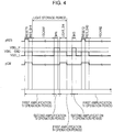
- Fig. 4 is a timing chart illustrating the operation of the circuit illustrated in Fig. 3 .
- the operation of the circuit illustrated in Fig. 3 will be described in detail with reference to the timing chart illustrated in Fig. 4 .
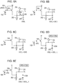
- Fig. 6A is a diagram illustrating a circuit in the region 50 surrounded by alternate long and short dashed lines in Fig. 3 .
- the connection state of the circuit illustrated in Fig. 6A is as illustrated in Fig. 6B .
- Fig. 6B when a switch or a transistor functioning as a switch is in the ON state (conductive state), two nodes, which are connected to each other by the switch or the transistor, are short-circuited with a solid line.
- the gate voltage and the source voltage of the second amplification Tr 205 are the same. Accordingly, the second amplification Tr 205 is in the OFF state, and the second source follower circuit is in the inactive state. On the other hand, the first amplification Tr 104 is in the ON state, and the first source follower circuit is in the active state. The first source follower circuit amplifies a signal corresponding to a reset voltage applied to the gate of the first amplification Tr 104 and outputs the amplified signal to the output signal line 110. At that time, the DAC 700 supplies a GND potential to the node VSEL.
- a noise signal is sampled in the intermediate capacitor 204.
- Fig. 6C is a diagram illustrating the connection state of the circuit illustrated in Fig. 6A in the period RES_SH1.
- the second amplification Tr 205 is also in the OFF state, and the first amplification Tr 104 is also in the ON state. That is, the first source follower circuit is in the active state, and the second source follower circuit is in the inactive state. Since the DAC 700 supplies a GND potential to the node VSEL, a noise signal is sampled in the intermediate capacitor 204 on the basis of the GND potential.
- Fig. 6D is a diagram illustrating the connection state of the circuit illustrated in Fig. 6A in the period HSCAN1.
- VPD represents the gate potential of the first amplification Tr 104
- VCM represents the gate potential of the second amplification Tr 205.
- the DAC 700 outputs a reference voltage VSEL_L to the node VSEL.
- the reference voltage VSEL_L maintains the relationship of VPD > VCM even if VPD is reduced by an electric charge generated by photoelectric conversion.
- the voltage of the output signal line 110 therefore becomes a voltage corresponding to the gate voltage of the first amplification Tr 104.
- the second amplification Tr 205 Since the gate voltage of the second amplification Tr 205 is lower than the source voltage of the second amplification Tr 205, the second amplification Tr 205 is in the OFF state. That is, like in the period RES_SH1, the second source follower circuit is in the inactive state and the first source follower circuit is in the active state.
- a period SHN the DAC 700 outputs to the node VSEL a reference voltage VSEL_H with which the relationship of VPD ⁇ VCM is maintained.
- Fig. 6E is a diagram illustrating the connection state of the circuit illustrated in Fig. 6A in the period SHN.
- a voltage corresponding to the gate voltage of the second amplification Tr 205 is output to the output signal line 110. Since the source voltage of the first amplification Tr 104 is higher than the gate voltage of the first amplification Tr 104, the first amplification Tr 104 is in the OFF state. Accordingly, the second source follower circuit including the second amplification Tr 205 and the current source 202 amplifies the noise signal stored in the intermediate capacitor 204 and outputs the amplified noise signal.
- a photoelectric conversion signal is sampled in the intermediate capacitor 204.
- the connection state of the circuit illustrated in Fig. 6A is as illustrated in Fig. 6C . That is, the second amplification Tr 205 is in the OFF state.
- the DAC 700 outputs to the node VSEL the reference voltage VSEL_H with which the relationship of VPD ⁇ VCM is maintained.
- the connection state of the circuit illustrated in Fig. 6A is as illustrated in Fig. 6E again. Since the second amplification Tr 205 is turned on, the second source follower circuit is brought into the active state and the photoelectric conversion signal stored in the intermediate capacitor 204 is output.
- the DAC 700 When the second source follower circuit outputs a photoelectric conversion signal and a noise signal, the DAC 700 outputs the same reference voltage VSEL_H. Accordingly, the signal values of the photoelectric conversion signal and the noise signal are determined on the basis of the same reference voltage.
- either the first source follower circuit or the second source follower circuit is in the active state when a sampling operation is performed on the intermediate capacitor 204 and a signal stored in the intermediate capacitor 204 is output. Accordingly, the current source 202 can be shared by the first amplification Tr 104 and the second amplification Tr 205, and the number of current sources can be reduced. This leads to the reduction in power consumption.
- the selection Tr 105 since the selection Tr 105 is not needed, the number of transistors in a pixel can be reduced. It is therefore possible to suppress the effect of desensitization of a photoelectric conversion unit caused by the reduction in the area of the photoelectric conversion unit.
- the DAC 700 As a reference voltage output circuit for generating a reference voltage to be supplied to the node VSEL, the DAC 700 is used. However, for example, a circuit capable of selecting a desired voltage using a plurality of switches may be used.
- a reference potential for the intermediate capacitor 204 is transitionally changed so as to switch between the ON state and the OFF state of each of the first amplification Tr 104 and the second amplification Tr 205.
- the value of a voltage to be applied to the gate of the first amplification Tr 104 may be transitionally controlled or the drain voltage of the first amplification Tr 104 or the second amplification Tr 205 may be controlled.
- both the first source follower circuit and the second source follower circuit may be temporarily in the active state.
- a selection unit may have a configuration capable of bringing a first amplification unit and a second amplification unit into the above-described state.
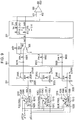
- Fig. 7 is a block diagram of a system according to the third embodiment.
- the same reference numerals are used to identify parts already described in the first embodiment, and the description thereof will be therefore omitted.
- the difference between the third embodiment and the first embodiment is the configuration of the pixel 101.
- the gate of the first amplification Tr 104 is connected to a floating diffusion (FD) 106.
- a transfer transistor (Tr) 107 is disposed between the PD 102 and the FD 106.
- a node TX is connected to the gate of the transfer Tr 107, and a transfer pulse pTX is input into the transfer Tr 107.
- the operation of the transfer Tr 107 is controlled by the transfer pulse pTX.
- a column amplification unit 901 is disposed between the column circuit block 201 and the storage unit 301.
- a column amplifier array 900 includes N column amplification units 901 that are one-dimensionally arranged.
- Each of the column amplification units 901 includes a clamp capacitor 902, a feedback capacitor 903, a reset switch 904, and an operational amplifier 905.
- One end of the clamp capacitor 902 is connected to the output signal line 110, and the other end of the clamp capacitor 902 is connected to an inverting input node of the operational amplifier 905.
- One end of the feedback capacitor 903 is connected to the inverting input node of the operational amplifier 905, and the other end of the feedback capacitor 903 is connected to an output node of the operational amplifier 905.
- the reset switch 904 is disposed so that it is parallel to the feedback capacitor 903. The reset switch 904 is controlled by a pulse input into a node pC0R.
- a non-inverting input node of the operational amplifier 905 is connected to a GND potential.
- the feedback capacitor 903 is formed of only one capacitor. However, in the feedback capacitor 903, a plurality of capacitors may be disposed in parallel to one another, and a switch connected in series to each of the capacitors may be disposed. By disposing sets of a capacitor and a switch in parallel to one another in the feedback capacitor 903, it is possible to switch between gains in the column amplification unit 901.
- a current source for supplying a bias current to the operational amplifier 905 is disposed in addition to the current source 202. That is, the operational amplifier 905 does not share a current source with both the first source follower circuit and the second source follower circuit.
- the operational amplifier 905 corresponds to a third amplification unit according to an embodiment of the present invention.
- Fig. 8 is a timing chart illustrating the operation of the circuit illustrated in Fig. 7 .
- the operation of the circuit illustrated in Fig. 7 will be described in detail with reference to the timing chart illustrated in Fig. 8 .
- a corresponding switch is turned on. It is assumed that the PD 102 has already performed light storage.
- pulses of levels at which corresponding transistors are turned on are individually input into the nodes RES, SEL, pCM, and pC0R.
- the potential of the FD 106 is reset.
- a pulse of a level at which the reset Tr 103 is turned off is input into the node RES.
- a noise component caused by the turning off of the reset Tr 103 is superimposed on a reset voltage for the FD 106.
- a noise signal output from the first source follower circuit is sampled in the intermediate capacitor 204. Since the source and the gate of the second source follower circuit are short-circuited, the second source follower circuit is in the inactive state.
- the transfer Tr 107 is turned off and a photoelectric conversion signal corresponding to the amount of electric charge transferred to the FD 106 is sampled in the intermediate capacitor 204.
- the first source follower circuit is in the active state and the second source follower circuit is in the inactive state.
- pulses of levels at which corresponding transistors are turned on are individually input into the nodes TX and RES.
- the reset Tr 103 and the transfer Tr 107 are brought into conduction and the potentials of the PD 102 and the FD 106 are reset.
- a pulse of a level at which the transfer Tr 107 is turned off is input into the node TX at the end of this period, and a light storage period starts.
- the photoelectric conversion signal sampled in the Cts 313 and the noise signal sampled in the Ctn 314 are transmitted to the horizontal output lines 402 and 401, respectively.
- the difference between the photoelectric conversion signal and the noise signal is obtained by the output amplifier 600 and is output from the output amplifier 600.
- the node of the clamp capacitor 902 on the side of the operational amplifier 905 is set to the GND potential using the amplification function of the operational amplifier 905 in the column amplification unit 901.
- an operational amplifier is operated when a signal is clamped in a clamp capacitor. That is, in this embodiment, the column amplification unit 901 operates as an amplification circuit when the first source follower circuit or the second source follower circuit is in the active state. Accordingly, the operational amplifier 905 included in the column amplification unit 901 does not share a current source with the first source follower circuit and the second source follower circuit.
- the pixel 101 includes the transfer Tr 107. Since the transfer Tr 107 can electrically disconnect the PD 102 from the FD 106, the PD 102 can store light in a state in which the potential of the FD 106 is maintained at a reset potential. Using this configuration, it is possible to reduce a time interval between sampling of a noise signal in the intermediate capacitor 204 and sampling of a photoelectric conversion signal in the intermediate capacitor 204. This leads to the reduction in the effect of 1/f noise.
- a system according to this embodiment includes the column amplification unit 901 including the clamp capacitor 902. Using this configuration, it is possible to reduce noise caused by variations of characteristics of the pixel 101 and the column circuit block 201.
- the storage unit 301 is disposed at a stage subsequent to the column amplification unit 901. Using this configuration, it is possible to reduce noise caused by variations of characteristic of the column amplification unit 901.
- Fig. 9 is a diagram illustrating an exemplary modification of a system according to the third embodiment.
- the same reference numerals are used to identify parts already described in the third embodiment, and the description thereof will be therefore omitted.
- Pixel arrays 100R, 100G, and 100B are disposed in three rows.
- the pixel arrays 100R, 100G, and 100B may output signals corresponding to red, green, blue lights, respectively.
- Fig. 9 only three pixels in a single column, pixels 101R, 101G, and 101B, are illustrated. However, a plurality of pixel columns may be disposed so as to achieve parallel reading.
- the column circuit block 201 and the clamp capacitor 902 are disposed for each pixel.
- the correspondence between a pixel and a component is represented by R, G, or B at the end of a numeral.
- the column circuit block 201 may be shared by some pixels.
- the column circuit block 201 may be shared by a pixel 101M used for monochrome image capturing and the pixel 101R corresponding to red light.
- the reset Trs 103R, 103G, and 103B in pixels are controlled by a common pulse.
- Selection Trs in pixels are similarly controlled by a common pulse.
- Transfer Trs in pixels are similarly controlled by a common pulse.
- S/H switches in column circuit blocks are similarly controlled by a common pulse.
- Column amplification switches 906R, 906G, and 906B are disposed on paths between the clamp capacitors 902R, 902G, and 902B and the inverting input terminal of the operational amplifier 905, respectively.
- the conductive states of the column amplification switch 906R, 906G, and 906B are controlled by pulses psw_r, psw_g, and psw_b, respectively.
- Fig. 10 is a timing chart illustrating the operation of the circuit illustrated in Fig. 9 .
- the operation of the circuit illustrated in Fig. 9 will be described in detail with reference to the timing chart illustrated in Fig. 10 . It is assumed that light storage has already started in a photoelectric conversion unit.
- pulses of levels at which corresponding switches are turned on are individually input into the column amplification switches 906R, 906G, and 906B.
- the noise signals of pixels written in the intermediate capacitors are individually clamped in clamp capacitors at the same time. At that time, the potentials of the nodes of the clamp capacitors on the side of the operational amplifier 905 are set to the GND potential.
- a pulse of a level at which the transfer Trs are turned on is input into the node TX, and signal electric charges generated in pixels in the light storage period are individually transferred to the FDs at the same time.
- the transfer Trs are turned off, the light storage period ends.
- the pulse psw_r of a level at which the column amplification switch 906R is turned on is input.
- the photoelectric conversion signal of the pixel 101R is clamped in the clamp capacitor 902R.
- a pulse of a level at which the Ct control switch 311 is turned on is input, and the photoelectric conversion signal of the pixel 101R is written in the Cts 313.
- the signals written in the Cts 313 and the Ctn 314 are individually transmitted to the horizontal output lines.
- the output amplifier 600 outputs a signal that does not include the offset component of the column amplifier.
- a pulse of a level at which the reset switch 904 is turned on is input, and the potential of the output node of the operational amplifier 905 is set to the GND potential.
- a pulse of a level at which the Ct control switch 312 is turned on is input and the offset component of the operational amplifier 905 is written in the Ctn 314.
- the pulse psw_g of a level at which the column amplification switch 906G is turned on is input.
- the photoelectric conversion signal of the pixel 101G is clamped in the clamp capacitor 902G.
- the Ct control switch 311 is brought into conduction, and the photoelectric conversion signal of the pixel 101G is written in the Cts 313. Signals are individually transmitted to the horizontal output lines, and the output amplifier 600 obtains the difference between these signals.
- the photoelectric conversion signal of the pixel 101B is read.
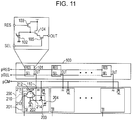
- Fig. 11 is a block diagram of a system according to the fourth embodiment.
- the same reference numerals are used to identify parts already described in the first to third embodiments, and the description thereof will be therefore omitted.
- a voltage follower circuit is disposed instead of a second source follower circuit according to the first embodiment. More specifically, a differential amplification circuit including two PMOS transistors (Trs) 211 and 212 and two NMOS transistors (Trs) 213 and 214 is disposed instead of the second amplification Tr 205 according to the first embodiment.
- the PMOS Trs 211 and 212, the NMOS Trs 213 and 214, and the current source 202 form an operational amplifier 210.
- the S/H switch 203 When the S/H switch 203 is in the ON state, the potentials of the gate and the source of the NMOS Tr 214 are the same. Since no current passes through the operational amplifier 210, the voltage follower circuit is in the inactive state. When the selection Tr 105 is in the ON state, the first source follower circuit in the active state amplifies a signal of a pixel and outputs the amplified signal to the intermediate capacitor 204.
- the first source follower circuit When the selection Tr 105 and the S/H switch 203 are in the OFF state, the first source follower circuit is in the inactive state. On the other hand, the voltage follower circuit in the active state amplifies a signal stored in the intermediate capacitor 204 and outputs the amplified signal. When the selection Tr 105 and the S/H switch 203 are turned off, the S/H switch 203 is turned off first.
- the selection Tr 105 and the S/H switch 203 correspond to a selection unit according to an embodiment of the present invention.
- a voltage follower circuit is used as a second amplification unit.
- the gain of a voltage follower circuit using an operational amplifier is close to 1. Accordingly, it is possible to improve a linear relationship between an input and an output and achieve image capturing of a high-quality image.
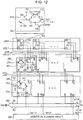
- Fig. 12 is a block diagram of a system according to the fifth embodiment.
- the same reference numerals are used to identify parts already described in the first to fourth embodiments, and the description thereof will be therefore omitted.
- the difference between the fifth embodiment and the first embodiment is that a first voltage follower circuit and a second voltage follower circuit are disposed instead of the first source follower circuit and the second source follower circuit, respectively.
- a first differential amplification circuit including two PMOS transistors 111 and 112 and two NMOS transistors 113 and 114 is disposed.
- the first differential amplification circuit is connected to the current source 202 via the selection Tr 105.
- the first differential amplification circuit and the current source 202 form the first voltage follower circuit.
- a second differential amplification circuit including the PMOS Trs 211 and 212 and the NMOS Trs 213 and 214 is connected to the current source 202 via a selection transistor (Tr) 215.
- the second differential amplification circuit and the current source 202 form the second voltage follower circuit.
- switching between the active state and the inactive state of the first voltage follower circuit is performed by switching between the ON state and the OFF state of the selection Tr 105
- switching between the active state and the inactive state of the second voltage follower circuit is performed by switching between the ON state and the OFF state of the selection Tr 215.
- the selection Trs 105 and 215 correspond to a selection unit according to an embodiment of the present invention.
- a voltage follower circuit including an operational amplifier is used.
- an amplification circuit having a voltage gain higher than 1 may be used.
- an electron is equivalent to a signal electric charge.
- a hole may be equivalent to a signal electric charge.
- the polarity of the PD 102 and the conductivity type of each transistor are reversed.
- the second embodiment even if a photodiode whose polarity is opposite to that of the PD 102 illustrated in Fig. 3 is used, it is possible to respond to the change of a photodiode by adjusting the voltage condition of the node VSEL.
- a signal is amplified by amplification units at two stages.
- a signal may be amplified by amplification units at more than two stages and a current source may be shared by these amplification units as appropriate.
- An apparatus includes converting means (102) configured to generate electric charge, first amplifying means (104, 202) configured to amplify a signal corresponding to an amount of the electric charge and output a first amplified signal, second amplifying means (205, 202) configured to amplify the first amplified signal and output a second amplified signal, a current source (202) shared by the first amplifying means and the second amplifying means, and selecting means (105, 203, 700, 215) configured to bring the first amplifying means and the second amplifying means into an inactive state.
- the current source is shared by the first amplifying means and the second amplifying means. The number of current sources is therefore reduced. This leads to the reduction in power consumption.
Description
- The present invention relates to a solid-state image pickup apparatus and a driving method therefor, and, more particularly, to a technique for reducing the power consumption of a solid-state image pickup apparatus.
- Solid-state image pickup apparatuses in which a signal generated by a photoelectric conversion unit is amplified by a plurality of amplification stages have been recently proposed. Japanese Patent Laid-Open No.
2006-109530 Fig. 1 .) - However, since two amplification stages individually have current sources in the photoelectric conversion apparatus, there is room for improvement from the viewpoint of power consumption. When more than two amplification stages are disposed, power consumption is further increased.
- In addition, in order to increase a signal reading speed, techniques for reading out signals from a plurality of pixels in parallel and amplifying them have been proposed. When a plurality of reading paths used to process signals in parallel are individually provided with a plurality of amplification stages, power consumption is increased in accordance with the number of reading circuits. For example, in solid-state image pickup apparatuses for copiers, scanners, and single-lens reflex cameras, thousands of reading paths may be disposed in parallel. In this case, power consumption is markedly increased.
Further related art is for example known from the documentUS 6,897,429 B1 relating to managing power consumption by sampling circuit current sources, and the documentUS 2004/0080637 A1 relating to a solid-state image pickup device and a control method therefore. - The present invention in its first aspect provides an apparatus as specified by the appended claims.
- Further features of the present invention will become apparent from the following description of exemplary embodiments with reference to the attached drawings.
-
-
Fig. 1 is a schematic diagram of a system according to a first embodiment of the present invention. -
Fig. 2 is a timing chart illustrating the operation of a solid-state image pickup apparatus illustrated inFig. 1 . -
Fig. 3 is a schematic diagram of a system according to a second embodiment of the present invention. -
Fig. 4 is a timing chart illustrating the operation of a solid-state image pickup apparatus illustrated inFig. 3 . -
Fig. 5A is a circuit diagram of a circuit block illustrated inFig. 1 . -
Figs. 5B to 5D are diagrams illustrating connection states of the circuit block illustrated inFig. 1 . -
Fig. 6A is a circuit diagram of the circuit block illustrated inFig. 3 . -
Figs. 6B to 6E are diagrams illustrating connection states of a circuit block illustrated inFig. 3 . -
Fig. 7 is a schematic diagram of a system according to a third embodiment of the present invention. -
Fig. 8 is a timing chart illustrating the operation of a solid-state image pickup apparatus illustrated inFig. 7 . -
Fig. 9 is a schematic diagram of a system that is an exemplary modification of the third embodiment. -
Fig. 10 is a timing chart illustrating the operation of a solid-state image pickup apparatus illustrated inFig. 9 . -
Fig. 11 is a schematic diagram of a system according to a fourth embodiment of the present invention. -
Fig. 12 is a schematic diagram of a system according to a fifth embodiment of the present invention. - Embodiments of the present invention will be described with reference to the accompanying drawings.
-
Fig. 1 is a block diagram of a system according to the first embodiment. Apixel array 100 includesN pixels 101 that are one-dimensionally arranged. Each of thepixels 101 includes a photodiode (PD) 102, a reset transistor (Tr) 103, a first amplification transistor (Tr) 104, and a selection transistor (Tr) 105. In this embodiment, each transistor is an NMOS transistor. Each transistor may be a PMOS transistor or a bipolar transistor as appropriate. - The
PD 102 is a photoelectric conversion unit for photoelectrically converting incident light into a signal electric charge. The gate of thefirst amplification Tr 104 is electrically connected to thePD 102. The drain of the first amplification Tr 104 is connected to a power line. The source of thefirst amplification Tr 104 is electrically connected to anoutput signal line 110 via theselection Tr 105. Thefirst amplification Tr 104 and acurrent source 202 to be described later form a first source follower circuit. The gate of thefirst amplification Tr 104 is an input node of the first source follower circuit. Thereset Tr 103 resets thePD 102 and the input node of the first source follower circuit. A node RES is connected to the gate of thereset Tr 103, and a reset pulse pRES is input into thereset Tr 103. The operation of thereset Tr 103 is controlled by the reset pulse pRES. - The first source follower circuit amplifies a signal corresponding to the amount of signal electric charge generated by the photoelectric conversion unit and outputs the amplified signal. In this specification, a signal corresponding to the amount of signal electric charge generated by a photoelectric conversion unit and a signal obtained by causing an amplification unit to amplify the signal are referred to as photoelectric conversion signals. In this embodiment, a photoelectric conversion signal output from the first source follower circuit corresponds to a first amplified signal according to an embodiment of the present invention.
- The first source follower circuit can output a pixel noise signal in a state in which the voltage of the input node thereof is reset to a reset voltage. In this specification, a signal corresponding to the voltage of an input node in a state in which the voltage of the input node is reset and a signal obtained by causing an amplification unit to amplify the signal are referred to as noise signals. The state in which the voltage of an input node is reset includes a sate in which the
reset Tr 103 connected to the input node is conducting and a state in which noise caused by turning off of thereset Tr 103 is superimposed. After thereset Tr 103 has been turned off, the voltage of the input node may be changed by an electric charge generated by photoelectric conversion. Even in this case, a state on the basis of which the difference between a photoelectric conversion signal and a noise signal is computed may be reset. A state immediately after thereset Tr 103 has been turned off is a reset state. In this embodiment, a noise signal output from the first source follower circuit corresponds to a third amplified signal according to an embodiment of the present invention. A signal output from thepixel 101 is output from an output node OUT and is then input into a circuit at a subsequent stage via theoutput signal line 110. - The
selection Tr 105 switches between an active state and an inactive state of the first source follower circuit. A node SEL is connected to the gate of theselection Tr 105, and a selection pulse pSEL is input into theselection Tr 105. The operation of theselection Tr 105 is controlled by the selection pulse pSEL. - A column
circuit block array 200 includes a plurality of column circuit blocks 201 that are individually connected to the output signal lines 110. The columncircuit block array 200 is configured to process signals output from a plurality of pixels in parallel. Each of the column circuit blocks 201 includes thecurrent source 202, a sample-and-hold (S/H)switch 203, anintermediate capacitor 204, and a second amplification transistor (Tr) 205. - The
second amplification Tr 205 and thecurrent source 202 form a second source follower circuit. The second source follower circuit amplifies a photoelectric conversion signal output from the first source follower circuit and outputs the amplified signal. A photoelectric conversion signal output from the second source follower circuit corresponds to a second amplified signal according to an embodiment of the present invention. In addition, the second source follower circuit may amplify a pixel noise signal and output the amplified pixel noise signal. A noise signal output from the second source follower circuit corresponds to a fourth amplified signal according to an embodiment of the present invention. - The S/
H switch 203 is disposed on a path between the output node OUT of thepixel 101, which is the output node of the first source follower circuit, and the gate of thesecond amplification Tr 205, which is the input node of the second source follower circuit. The S/H switch 203 may be disposed to directly connect the output node OUT and the gate of thesecond amplification Tr 205 or to connect the output node OUT and the gate ofsecond amplification Tr 205 via another circuit element. The S/H switch 203 is switched between an ON state and an OFF state by an S/H pulse input into a node pCM. The S/H switch 203 controls the electric connection between the output node of the first source follower circuit and the input node of the second source follower circuit. - The
intermediate capacitor 204 is disposed as appropriate, and is used to temporarily store a photoelectric conversion signal output from the first source follower circuit. The intermediate capacitor is formed of a capacitance element in this embodiment, but may be formed of a parasitic capacitor between lines. Theintermediate capacitor 204 may store a noise signal output from the first source follower circuit. - The
current source 202 is a load for supplying a driving current for an amplification circuit, and is formed of a transistor or the like. Thefirst amplification Tr 104 and thesecond amplification Tr 205 share thecurrent source 202 with each other so as to form the first source follower circuit and the second source follower circuit, respectively. As will be described in detail later, in this embodiment, theselection Tr 105 switches between the active state and the inactive state of the first source follower circuit, and the S/H switch 203 switches between the active state and the inactive state of the second source follower circuit. Theselection Tr 105 and the S/H switch 203 correspond to a selection unit according to an embodiment of the present invention. - In general, amplification circuits include at least one transistor and a bias supply for supplying a bias current or a bias voltage to the transistor. Examples of a bias supply for supplying a bias current include a current source. As a method of bringing an amplification circuit into an inactive state, a method of controlling the bias state of a transistor included in the amplification circuit so that the transistor is turned off or a method of electrically disconnecting the amplification circuit with a switch disposed in the amplification circuit can be considered. For example, it is possible to bring an amplification circuit into an inactive state by interrupting the path between a transistor and a bias supply with a switch.
- A selection unit according to this embodiment can bring the second source follower circuit into the inactive state when the first source follower circuit is in the active state, and can bring the first source follower circuit into the inactive state when the second source follower circuit in the active state.
- The selection unit may bring both the first source follower circuit and the source follower circuit into the inactive state at the same time. For example, the selection unit can bring the first source follower circuit and the source follower circuit into the inactive state by bringing the
selection Tr 105 into the non-conductive state and bringing the S/H switch 203 into the conductive state. - Each of the
selection Tr 105 and the S/H switch 203 transitionally switches between the conductive state and the non-conductive state. Accordingly, during a period of transition, it may not be determined which of the first source follower circuit and the second source follower circuit is in the inactive state or both the first source follower circuit and the second source follower may be in the active state. The selection unit may have a configuration capable of bringing a first amplification unit and a second amplification unit in the above-described state. - A
storage unit 301 for storing a photoelectric conversion signal and a noise signal is disposed for each of theoutput signal lines 110 as appropriate. Amemory array 300 includes thestorage units 301. Thestorage unit 301 includes a storage capacitor (Cts) 313 for storing a photoelectric conversion signal, a storage capacitor (Ctn) 314 for storing a noise signal, aCt control switch 311 for controlling sampling of a signal in theCts 313, aCt control switch 312 for controlling sampling of a signal in theCtn 314, ahorizontal scanning switch 315 for controlling output of a signal to ahorizontal output line 402, and ahorizontal scanning switch 316 for controlling output of a signal to ahorizontal output line 401. The Ct control switches 311 and 312 are controlled by control signals pTS and pTN, respectively. The horizontal scanning switches 315 and 316 are controlled by a horizontal scanning signal hsr<1>, ···, or hsr<n> (n represents a column number) generated by ahorizontal scanning circuit 500. - At a subsequent stage of the
horizontal output lines output amplifier 600 for outputting the difference between a signal output to thehorizontal output line 401 and a signal output to thehorizontal output line 402 is disposed as appropriate. By outputting the difference between a noise signal and a photoelectric conversion signal containing a noise component correlated with noise of a pixel, it is possible to obtain a signal corresponding to a net amount of electric charge generated by photoelectric conversion. -
Fig. 2 is a timing chart illustrating the operation of the circuit illustrated inFig. 1 . Pulses with the same reference numeral inFigs. 1 and2 correspond to each other. Referring toFig. 2 , a horizontal axis represents a time. The operation of the system illustrated inFig. 1 will be described in detail with reference to the timing chart illustrated inFig. 2 . When each pulse is at a high level, a corresponding switch is turned on. It is assumed that a signal that has been obtained in the last storage period is stored in thestorage unit 301. - In a period RESET1, pulses of levels at which switches corresponding to the nodes RES, SEL, and pCM are turned on are input into the nodes RES, SEL, and pCM, respectively. The
reset Tr 103 is brought into the conductive state after the pulse has been input into the node RES, so that the potential of thePD 102 and the potential of the gate of thefirst amplification Tr 104, that is, the potential of the input node of the first source follower circuit, are reset. -
Fig. 5A is a diagram illustrating a circuit in aregion 50 surrounded by alternate long and short dashed lines inFig. 1 .Fig. 5B is a diagram illustrating the connection state of the circuit illustrated inFig. 5A in the period RESET1. Referring toFig. 5B , when a switch or a transistor functioning as a switch is in the ON state (conductive state), two nodes, which are connected to each other by the switch or the transistor, are short-circuited with a solid line. When a switch or a transistor functioning as a switch is in the OFF state (non-conductive state), there is no solid line between two nodes that are connected to each other by the switch or the transistor. Thus, inFig. 5B and other drawings, the representation of a circuit is simplified. - Referring to
Fig. 5B , the gate voltage and the source voltage of thesecond amplification Tr 205 are the same. Accordingly, thesecond amplification Tr 205 is in the OFF state and does not affect the output of a pixel. That is, the second source follower circuit does not perform an amplification operation and is in the inactive state. On the other hand, the first source follower circuit including thefirst amplification Tr 104 is in the active state. The first source follower circuit amplifies a signal corresponding to a reset voltage applied to the gate of thefirst amplification Tr 104, which it the input portion of the first source follower circuit, and outputs the amplified signal to theoutput signal line 110. - In a period RES_SH1 illustrated in
Fig. 2 , a pulse of a level at which thereset Tr 103 is turned off is input into the node RES. Turning off of thereset Tr 103 generates a noise component and the noise component is superimposed on a reset voltage. A noise signal output from the first source follower circuit is sampled in theintermediate capacitor 204. In this embodiment, after the period RES_SH1 has elapsed, a light storage period is started. -
Fig. 5C illustrates the connection state of the circuit illustrated inFig. 5A in the period RES_SH1. In this period, the first source follower circuit is also in the active state, and the second source follower circuit is also in the inactive state. - In a period HSCAN1, pulses of levels at which switches corresponding to the nodes SEL and pCM are turned off are input into the nodes SEL and pCM, respectively. In this period, a photoelectric conversion signal and a noise signal, which have been stored in the
Cts 313 and theCtn 314, respectively, in the last light storage period, are externally output from theoutput amplifier 600 via thehorizontal output lines -
Fig. 5D is a diagram illustrating the connection state of the circuit illustrated inFig. 5A in the period HSCAN1. Referring toFig. 5D , the S/H switch 203 is in the OFF state, and the source and the gate of thesecond amplification Tr 205 are not connected. Here, by setting the level of a signal amplified by the first source follower circuit to a level at which thesecond amplification Tr 205 can operate in a saturation region, thesecond amplification Tr 205 is turned on. That is, the second source follower circuit is brought into the active state, receives the noise signal stored in theintermediate capacitor 204, amplifies the noise signal, and outputs the amplified noise signal to theoutput signal line 110. On the other hand, the first source follower circuit is in the inactive state since theselection Tr 105 electrically disconnects thefirst amplification Tr 104 from thecurrent source 202. - In a period SHN, a pulse of a level at which the
Ct control switch 312 is turned on is input into a node pTN. In this period, the connection state of the circuit illustrated inFig. 5A is as illustrated inFig. 5D . The second source follower circuit including thesecond amplification Tr 205 and thecurrent source 202 amplifies the noise signal stored in theintermediate capacitor 204 and samples the amplified signal in theCtn 314. - After the noise signal has been sampled in the
Ctn 314, pulses of levels at which switches corresponding to the nodes SEL and pCM are turned on are input into the nodes SEL and pCM, respectively. In a period LIGHT_SH, like in the period RES_SH1, the connection state of the circuit illustrated inFig. 5A is as illustrated inFig. 5C . That is, the second source follower circuit is in the inactive state, and the first source follower circuit is in the active state. A photoelectric conversion signal amplified by the first source follower circuit is sampled in theintermediate capacitor 204. After the period LIGHT_SH has elapsed, the light storage period ends. - In a period SHS, pulses of levels at which switches corresponding to the nodes SEL and pCM are turned off are input into the nodes SEL and pCM, respectively, and a pulse of a level at which the
Ct control switch 311 is turned on is input into a node pTS. At that time, the connection state of the circuit illustrated inFig. 5A is as illustrated inFig. 5D . That is, the second source follower circuit is in the active state, and the photoelectric conversion signal is sampled in theCts 313. - In periods RESET2 and RES_SH2, a reset operation and a noise signal sampling operation are performed. In a period HSCAN2, the photoelectric conversion signal sampled in the
Cts 313 and the noise signal sampled in theCtn 314 are read out. - A pulse input into the node pSEL and a pulse input into the node pCM can be separately controlled. Accordingly, the switching between the active state and the inactive state of each of the first source follower circuit and the second source follower circuit can be controlled regardless of the conductive state of the other source follower circuit. Such control can be achieved with a control pulse transmitted from a timing generator disposed in a solid-state image pickup apparatus or a control pulse externally transmitted from a CPU or the like.
- As described previously, in this embodiment, when sampling processing is performed on a capacitor such as the
intermediate capacitor 204, theCts 313, or theCtn 314, either the first source follower circuit or the second source follower circuit is in the active state. In particular, when an amplified signal is sampled in a signal storage unit (theintermediate capacitor 204 or the storage unit 301) disposed at a stage subsequent to each of source follower circuits, both of these source follower circuits are not in the active state. As a result, it is possible for thefirst amplification Tr 104 and thesecond amplification Tr 205 to share thecurrent source 202 without increasing power consumption. According to this embodiment, as compared with the related art, the number of current sources can be reduced. This leads to the reduction in power consumption. - In this embodiment, the number of required elements may be reduced by achieving the sharing of a current source. This leads to the size reduction of a solid-state image pickup element.
- In this embodiment, the output node of the first source follower circuit and the output node of the second source follower circuit are connected to the
output signal line 110. - The
output signal line 110 is connected to thecurrent source 202. Using this configuration, it is possible to reduce the number of lines in circuits. This leads to the size reduction of a solid-state image pickup element. - In this embodiment, the
storage unit 301 includes theCts 313 and theCtn 314. Using this configuration, a photoelectric conversion signal can be stored in theCts 313, a noise signal can be stored in theCtn 314, and the difference between the photoelectric conversion signal and the noise signal can be output from theoutput amplifier 600. It is therefore possible to reduce noise cause by variations of characteristics of transistors in a pixel. - In this embodiment, instead of a noise signal and a photoelectric conversion signal, signals correlated with each other with regard to pixel resetting may be input into the
output amplifier 600. Since theoutput amplifier 600 outputs the difference between these signals, pixel resetting noise included in a signal output from theoutput amplifier 600 is reduced. Using this configuration, it is possible to capture a high-quality and low-noise image. - In this embodiment, the
selection Tr 105 is connected to thefirst amplification Tr 104 and theoutput signal line 110. However, for example, theselection Tr 105 may be connected to a path between a power supply line and the drain of thefirst amplification Tr 104. - Power supply voltages for the first source follower circuit and the second source follower circuit are not necessarily the same, and may differ from each other so as to allow these circuits to efficiently perform operations in operation ranges.
- In this embodiment, the
pixel 101 may have a floating diffusion (FD) unit at a node between thePD 102 and thefirst amplification Tr 104. In this embodiment, the configuration of a reading circuit disposed at a stage subsequent to a line memory is not limited to the configuration illustrated inFig. 1 . For example, at a stage subsequent to the columncircuit block array 200, an amplification circuit such as a switched capacitor amplifier or an analog-to-digital converter (ADC) may be disposed. -
Fig. 3 is a block diagram of a system according to the second embodiment. The same reference numerals are used to identify parts already described in the first embodiment, and the description thereof will be therefore omitted. The difference between the first embodiment and the second embodiment will be described. - In this embodiment, the
pixel 101 includes thePD 102, thereset Tr 103, and thefirst amplification Tr 104 that is included in a first source follower circuit. The difference between the second embodiment and the first embodiment is that thepixel 101 does not include theselection Tr 105. - The
column circuit block 201 includes thecurrent source 202, the S/H switch 203, theintermediate capacitor 204, and thesecond amplification Tr 205. One terminal of theintermediate capacitor 204 is connected to a path between the S/H switch 203 and the gate of thesecond amplification Tr 205, and the other terminal of theintermediate capacitor 204 is connected to a node VSEL. A reference potential generated by a digital-to-analog converter (DAC) 700 is input into the node VSEL. In this embodiment, the sizes of thefirst amplification Tr 104 and thesecond amplification Tr 205 are the same. - A circuit at a stage subsequent to the column
circuit block array 200 is not illustrated inFig. 3 . A circuit similar to that according to the first embodiment or a circuit in the related art may be disposed at a stage subsequent to the columncircuit block array 200. - As will be described in detail later, the
DAC 700 brings the first source follower circuit into the inactive state, and the S/H switch 203 brings the second source follower circuit into the inactive state. In this embodiment, the S/H switch 203 and theDAC 700 correspond to a selection unit according to an embodiment of the present invention. -
Fig. 4 is a timing chart illustrating the operation of the circuit illustrated inFig. 3 . The operation of the circuit illustrated inFig. 3 will be described in detail with reference to the timing chart illustrated inFig. 4 . - Referring to
Fig. 4 , in a period RESET1, thePD 102 is reset.Fig. 6A is a diagram illustrating a circuit in theregion 50 surrounded by alternate long and short dashed lines inFig. 3 . In the period RESET1, the connection state of the circuit illustrated inFig. 6A is as illustrated inFig. 6B . Referring toFig. 6B , when a switch or a transistor functioning as a switch is in the ON state (conductive state), two nodes, which are connected to each other by the switch or the transistor, are short-circuited with a solid line. When a switch or a transistor functioning as a switch is in the OFF state (non-conductive state), there is no solid line between two nodes that are connected to each other by the switch or the transistor. Thus, inFig. 6B and other drawings, the representation of a circuit is simplified. - Referring to
Fig. 6B , the gate voltage and the source voltage of thesecond amplification Tr 205 are the same. Accordingly, thesecond amplification Tr 205 is in the OFF state, and the second source follower circuit is in the inactive state. On the other hand, thefirst amplification Tr 104 is in the ON state, and the first source follower circuit is in the active state. The first source follower circuit amplifies a signal corresponding to a reset voltage applied to the gate of thefirst amplification Tr 104 and outputs the amplified signal to theoutput signal line 110. At that time, theDAC 700 supplies a GND potential to the node VSEL. - In a period RES_SH1, a noise signal is sampled in the
intermediate capacitor 204.Fig. 6C is a diagram illustrating the connection state of the circuit illustrated inFig. 6A in the period RES_SH1. In this period, thesecond amplification Tr 205 is also in the OFF state, and thefirst amplification Tr 104 is also in the ON state. That is, the first source follower circuit is in the active state, and the second source follower circuit is in the inactive state. Since theDAC 700 supplies a GND potential to the node VSEL, a noise signal is sampled in theintermediate capacitor 204 on the basis of the GND potential. - In a period HSCAN1, an electric charge is stored in a photoelectric conversion unit.
Fig. 6D is a diagram illustrating the connection state of the circuit illustrated inFig. 6A in the period HSCAN1. InFig. 6D , VPD represents the gate potential of thefirst amplification Tr 104, and VCM represents the gate potential of thesecond amplification Tr 205. In the period HSCAN1 illustrated inFig. 4 , theDAC 700 outputs a reference voltage VSEL_L to the node VSEL. The reference voltage VSEL_L maintains the relationship of VPD > VCM even if VPD is reduced by an electric charge generated by photoelectric conversion. The voltage of theoutput signal line 110 therefore becomes a voltage corresponding to the gate voltage of thefirst amplification Tr 104. Since the gate voltage of thesecond amplification Tr 205 is lower than the source voltage of thesecond amplification Tr 205, thesecond amplification Tr 205 is in the OFF state. That is, like in the period RES_SH1, the second source follower circuit is in the inactive state and the first source follower circuit is in the active state. - In a period SHN, the
DAC 700 outputs to the node VSEL a reference voltage VSEL_H with which the relationship of VPD < VCM is maintained.Fig. 6E is a diagram illustrating the connection state of the circuit illustrated inFig. 6A in the period SHN. InFig. 6E , since the relationship of VPD < VCM is maintained, a voltage corresponding to the gate voltage of thesecond amplification Tr 205 is output to theoutput signal line 110. Since the source voltage of thefirst amplification Tr 104 is higher than the gate voltage of thefirst amplification Tr 104, thefirst amplification Tr 104 is in the OFF state. Accordingly, the second source follower circuit including thesecond amplification Tr 205 and thecurrent source 202 amplifies the noise signal stored in theintermediate capacitor 204 and outputs the amplified noise signal. - In a period LIGHT_SH, a photoelectric conversion signal is sampled in the
intermediate capacitor 204. At that time, like in the period RES_SH1, the connection state of the circuit illustrated inFig. 6A is as illustrated inFig. 6C . That is, thesecond amplification Tr 205 is in the OFF state. - In a period SHS, the
DAC 700 outputs to the node VSEL the reference voltage VSEL_H with which the relationship of VPD < VCM is maintained. The connection state of the circuit illustrated inFig. 6A is as illustrated inFig. 6E again. Since thesecond amplification Tr 205 is turned on, the second source follower circuit is brought into the active state and the photoelectric conversion signal stored in theintermediate capacitor 204 is output. - When the second source follower circuit outputs a photoelectric conversion signal and a noise signal, the
DAC 700 outputs the same reference voltage VSEL_H. Accordingly, the signal values of the photoelectric conversion signal and the noise signal are determined on the basis of the same reference voltage. - In periods RESET2 and RES_SH2, a reset operation and a noise signal sampling operation are performed.
- As described previously, in this embodiment, by controlling a reference potential for the
intermediate capacitor 204, either the first source follower circuit or the second source follower circuit is in the active state when a sampling operation is performed on theintermediate capacitor 204 and a signal stored in theintermediate capacitor 204 is output. Accordingly, thecurrent source 202 can be shared by thefirst amplification Tr 104 and thesecond amplification Tr 205, and the number of current sources can be reduced. This leads to the reduction in power consumption. - In this embodiment, since the
selection Tr 105 is not needed, the number of transistors in a pixel can be reduced. It is therefore possible to suppress the effect of desensitization of a photoelectric conversion unit caused by the reduction in the area of the photoelectric conversion unit. - In this embodiment, as a reference voltage output circuit for generating a reference voltage to be supplied to the node VSEL, the
DAC 700 is used. However, for example, a circuit capable of selecting a desired voltage using a plurality of switches may be used. - In this embodiment, a reference potential for the
intermediate capacitor 204 is transitionally changed so as to switch between the ON state and the OFF state of each of thefirst amplification Tr 104 and thesecond amplification Tr 205. However, for example, in order to switch between the ON state and the OFF state of each of thefirst amplification Tr 104 and thesecond amplification Tr 205, the value of a voltage to be applied to the gate of thefirst amplification Tr 104 may be transitionally controlled or the drain voltage of thefirst amplification Tr 104 or thesecond amplification Tr 205 may be controlled. - Since a reference potential for the
intermediate capacitor 204 is transitionally changed, both the first source follower circuit and the second source follower circuit may be temporarily in the active state. A selection unit may have a configuration capable of bringing a first amplification unit and a second amplification unit into the above-described state. -
Fig. 7 is a block diagram of a system according to the third embodiment. The same reference numerals are used to identify parts already described in the first embodiment, and the description thereof will be therefore omitted. - The difference between the third embodiment and the first embodiment is the configuration of the
pixel 101. The gate of thefirst amplification Tr 104 is connected to a floating diffusion (FD) 106. A transfer transistor (Tr) 107 is disposed between thePD 102 and theFD 106. - A node TX is connected to the gate of the
transfer Tr 107, and a transfer pulse pTX is input into thetransfer Tr 107. The operation of thetransfer Tr 107 is controlled by the transfer pulse pTX. When thetransfer Tr 107 is brought into the conductive state, an electric charge stored in thePD 102 is depletion-transferred to theFD 106. An electric charge is to be completely depletion-transferred from thePD 102 to theFD 106. - A
column amplification unit 901 is disposed between thecolumn circuit block 201 and thestorage unit 301. Acolumn amplifier array 900 includes Ncolumn amplification units 901 that are one-dimensionally arranged. Each of thecolumn amplification units 901 includes aclamp capacitor 902, afeedback capacitor 903, areset switch 904, and anoperational amplifier 905. - One end of the
clamp capacitor 902 is connected to theoutput signal line 110, and the other end of theclamp capacitor 902 is connected to an inverting input node of theoperational amplifier 905. One end of thefeedback capacitor 903 is connected to the inverting input node of theoperational amplifier 905, and the other end of thefeedback capacitor 903 is connected to an output node of theoperational amplifier 905. Thereset switch 904 is disposed so that it is parallel to thefeedback capacitor 903. Thereset switch 904 is controlled by a pulse input into a node pC0R. A non-inverting input node of theoperational amplifier 905 is connected to a GND potential. - In the circuit illustrated in
Fig. 7 , thefeedback capacitor 903 is formed of only one capacitor. However, in thefeedback capacitor 903, a plurality of capacitors may be disposed in parallel to one another, and a switch connected in series to each of the capacitors may be disposed. By disposing sets of a capacitor and a switch in parallel to one another in thefeedback capacitor 903, it is possible to switch between gains in thecolumn amplification unit 901. - Although not illustrated, a current source for supplying a bias current to the
operational amplifier 905 is disposed in addition to thecurrent source 202. That is, theoperational amplifier 905 does not share a current source with both the first source follower circuit and the second source follower circuit. Theoperational amplifier 905 corresponds to a third amplification unit according to an embodiment of the present invention. -
Fig. 8 is a timing chart illustrating the operation of the circuit illustrated inFig. 7 . The operation of the circuit illustrated inFig. 7 will be described in detail with reference to the timing chart illustrated inFig. 8 . When each pulse is at a high level, a corresponding switch is turned on. It is assumed that thePD 102 has already performed light storage. - Referring to
Fig. 8 , in a period between t0 and t1, pulses of levels at which corresponding transistors are turned on are individually input into the nodes RES, SEL, pCM, and pC0R. As a result, the potential of theFD 106 is reset. - In a period between t1 and t2, a pulse of a level at which the
reset Tr 103 is turned off is input into the node RES. A noise component caused by the turning off of thereset Tr 103 is superimposed on a reset voltage for theFD 106. At that time, a noise signal output from the first source follower circuit is sampled in theintermediate capacitor 204. Since the source and the gate of the second source follower circuit are short-circuited, the second source follower circuit is in the inactive state. - In a period between t2 and t3, pulses of levels at which corresponding transistors are turned off are individually input into the nodes SEL and pCM. As a result, the second source follower circuit is brought into the active state. The noise signal stored in the
intermediate capacitor 204 is amplified by the second source follower circuit and is then sampled in theclamp capacitor 902. Since theselection Tr 105 is in the OFF state, the first source follower circuit is in the inactive state. - In a period between t4 and t5, a pulse of a level at which the
Ct control switch 312 is turned on is input into the node pTN. As a result, a noise signal is stored in theCtn 314. - In a period between t6 and t7, pulses of levels at which corresponding switches are turned on are individually input into the nodes TX, SEL and pCM. Since the
transfer Tr 107 is brought into conduction, a signal electric charge stored in thePD 102 is transferred to theFD 106. After this period has elapsed, a light storage period ends. - In a period between t7 and t8, the
transfer Tr 107 is turned off and a photoelectric conversion signal corresponding to the amount of electric charge transferred to theFD 106 is sampled in theintermediate capacitor 204. At that time, the first source follower circuit is in the active state and the second source follower circuit is in the inactive state. - In a period between t8 and t9, pulses of levels at which corresponding switches are turned off are individually input into the nodes SEL and pCM. As a result, the second source follower circuit is brought into the active state and the difference between a noise signal and the photoelectric conversion signal stored in the
intermediate capacitor 204 is stored in theclamp capacitor 902. - In a period between t9 and t10, a pulse of a level at which the
Ct control switch 311 is turned on is input into the node pTS. As a result, a photoelectric conversion signal is sampled in theCts 313. - In a period between t11 and t12, pulses of levels at which corresponding transistors are turned on are individually input into the nodes TX and RES. As a result, the
reset Tr 103 and thetransfer Tr 107 are brought into conduction and the potentials of thePD 102 and theFD 106 are reset. A pulse of a level at which thetransfer Tr 107 is turned off is input into the node TX at the end of this period, and a light storage period starts. - In a period between t13 and t14, the photoelectric conversion signal sampled in the
Cts 313 and the noise signal sampled in theCtn 314 are transmitted to thehorizontal output lines output amplifier 600 and is output from theoutput amplifier 600. - In this embodiment, when the second source follower circuit writes a noise signal stored in the intermediate capacitor into the
clamp capacitor 902, the node of theclamp capacitor 902 on the side of theoperational amplifier 905 is set to the GND potential using the amplification function of theoperational amplifier 905 in thecolumn amplification unit 901. Thus, an operational amplifier is operated when a signal is clamped in a clamp capacitor. That is, in this embodiment, thecolumn amplification unit 901 operates as an amplification circuit when the first source follower circuit or the second source follower circuit is in the active state. Accordingly, theoperational amplifier 905 included in thecolumn amplification unit 901 does not share a current source with the first source follower circuit and the second source follower circuit. - In this embodiment, the following effect can be obtained in addition to the effect that can be obtained in the first embodiment. In this embodiment, the
pixel 101 includes thetransfer Tr 107. Since thetransfer Tr 107 can electrically disconnect thePD 102 from theFD 106, thePD 102 can store light in a state in which the potential of theFD 106 is maintained at a reset potential. Using this configuration, it is possible to reduce a time interval between sampling of a noise signal in theintermediate capacitor 204 and sampling of a photoelectric conversion signal in theintermediate capacitor 204. This leads to the reduction in the effect of 1/f noise. - A system according to this embodiment includes the
column amplification unit 901 including theclamp capacitor 902. Using this configuration, it is possible to reduce noise caused by variations of characteristics of thepixel 101 and thecolumn circuit block 201. - In this embodiment, the
storage unit 301 is disposed at a stage subsequent to thecolumn amplification unit 901. Using this configuration, it is possible to reduce noise caused by variations of characteristic of thecolumn amplification unit 901. -
Fig. 9 is a diagram illustrating an exemplary modification of a system according to the third embodiment. The same reference numerals are used to identify parts already described in the third embodiment, and the description thereof will be therefore omitted. - Pixel arrays 100R, 100G, and 100B are disposed in three rows. For example, the pixel arrays 100R, 100G, and 100B may output signals corresponding to red, green, blue lights, respectively. In
Fig. 9 , only three pixels in a single column,pixels - The
column circuit block 201 and theclamp capacitor 902 are disposed for each pixel. The correspondence between a pixel and a component is represented by R, G, or B at the end of a numeral. Thecolumn circuit block 201 may be shared by some pixels. For example, thecolumn circuit block 201 may be shared by a pixel 101M used for monochrome image capturing and thepixel 101R corresponding to red light. - The
reset Trs - Column amplification switches 906R, 906G, and 906B are disposed on paths between the
clamp capacitors operational amplifier 905, respectively. The conductive states of thecolumn amplification switch -
Fig. 10 is a timing chart illustrating the operation of the circuit illustrated inFig. 9 . The operation of the circuit illustrated inFig. 9 will be described in detail with reference to the timing chart illustrated inFig. 10 . It is assumed that light storage has already started in a photoelectric conversion unit. - After the reset Trs have been turned off and noise signals have been written in the intermediate capacitors, pulses of levels at which corresponding switches are turned on are individually input into the column amplification switches 906R, 906G, and 906B. The noise signals of pixels written in the intermediate capacitors are individually clamped in clamp capacitors at the same time. At that time, the potentials of the nodes of the clamp capacitors on the side of the
operational amplifier 905 are set to the GND potential. - After the
reset switch 904 has been turned off, a pulse of a level at which theCt control switch 312 is turned on is input and the offset component of theoperational amplifier 905 is written in theCtn 314. - A pulse of a level at which the transfer Trs are turned on is input into the node TX, and signal electric charges generated in pixels in the light storage period are individually transferred to the FDs at the same time. When the transfer Trs are turned off, the light storage period ends.
- After the signal electric charges have been transferred to the FDs, the pulse psw_r of a level at which the
column amplification switch 906R is turned on is input. As a result, the photoelectric conversion signal of thepixel 101R is clamped in theclamp capacitor 902R. Subsequently, a pulse of a level at which theCt control switch 311 is turned on is input, and the photoelectric conversion signal of thepixel 101R is written in theCts 313. The signals written in theCts 313 and theCtn 314 are individually transmitted to the horizontal output lines. Theoutput amplifier 600 outputs a signal that does not include the offset component of the column amplifier. - Subsequently, a pulse of a level at which the
reset switch 904 is turned on is input, and the potential of the output node of theoperational amplifier 905 is set to the GND potential. After theoperational amplifier 905 has been reset, a pulse of a level at which theCt control switch 312 is turned on is input and the offset component of theoperational amplifier 905 is written in theCtn 314. - Subsequently, the pulse psw_g of a level at which the
column amplification switch 906G is turned on is input. As a result, the photoelectric conversion signal of thepixel 101G is clamped in theclamp capacitor 902G. Subsequently, theCt control switch 311 is brought into conduction, and the photoelectric conversion signal of thepixel 101G is written in theCts 313. Signals are individually transmitted to the horizontal output lines, and theoutput amplifier 600 obtains the difference between these signals. - After the offset component of the
operational amplifier 905 has been read, like the photoelectric conversion signals of thepixels pixel 101B is read. - The following effect can be obtained in addition to the effect that can be obtained in the third embodiment. In this exemplary modification of the third embodiment, after all pixels have been reset at the same time, photoelectric conversion signals of these pixels can be individually written in the intermediate capacitors at the same time. Using this configuration, it is possible to set the same light storage period in all pixels even if the pixels are arranged in a plurality of rows.
-
Fig. 11 is a block diagram of a system according to the fourth embodiment. The same reference numerals are used to identify parts already described in the first to third embodiments, and the description thereof will be therefore omitted. - In this embodiment, a voltage follower circuit is disposed instead of a second source follower circuit according to the first embodiment. More specifically, a differential amplification circuit including two PMOS transistors (Trs) 211 and 212 and two NMOS transistors (Trs) 213 and 214 is disposed instead of the
second amplification Tr 205 according to the first embodiment. ThePMOS Trs 211 and 212, theNMOS Trs current source 202 form anoperational amplifier 210. - When the S/
H switch 203 is in the ON state, the potentials of the gate and the source of theNMOS Tr 214 are the same. Since no current passes through theoperational amplifier 210, the voltage follower circuit is in the inactive state. When theselection Tr 105 is in the ON state, the first source follower circuit in the active state amplifies a signal of a pixel and outputs the amplified signal to theintermediate capacitor 204. - When the
selection Tr 105 and the S/H switch 203 are in the OFF state, the first source follower circuit is in the inactive state. On the other hand, the voltage follower circuit in the active state amplifies a signal stored in theintermediate capacitor 204 and outputs the amplified signal. When theselection Tr 105 and the S/H switch 203 are turned off, the S/H switch 203 is turned off first. - In this embodiment, the
selection Tr 105 and the S/H switch 203 correspond to a selection unit according to an embodiment of the present invention. - In this embodiment, a voltage follower circuit is used as a second amplification unit. Using this configuration, the following effect can be obtained in addition to the effect that can be obtained in the first embodiment. The gain of a voltage follower circuit using an operational amplifier is close to 1. Accordingly, it is possible to improve a linear relationship between an input and an output and achieve image capturing of a high-quality image.
- In this embodiment, a configuration according to the second or third embodiment may be employed.
-
Fig. 12 is a block diagram of a system according to the fifth embodiment. The same reference numerals are used to identify parts already described in the first to fourth embodiments, and the description thereof will be therefore omitted. - The difference between the fifth embodiment and the first embodiment is that a first voltage follower circuit and a second voltage follower circuit are disposed instead of the first source follower circuit and the second source follower circuit, respectively. Instead of the
first amplification Tr 104 in thepixel 101, a first differential amplification circuit including twoPMOS transistors NMOS transistors 113 and 114 is disposed. The first differential amplification circuit is connected to thecurrent source 202 via theselection Tr 105. The first differential amplification circuit and thecurrent source 202 form the first voltage follower circuit. - A second differential amplification circuit including the
PMOS Trs 211 and 212 and theNMOS Trs current source 202 via a selection transistor (Tr) 215. The second differential amplification circuit and thecurrent source 202 form the second voltage follower circuit. - In this embodiment, switching between the active state and the inactive state of the first voltage follower circuit is performed by switching between the ON state and the OFF state of the
selection Tr 105, and switching between the active state and the inactive state of the second voltage follower circuit is performed by switching between the ON state and the OFF state of theselection Tr 215. Theselection Trs - Using this configuration, it is possible to further improve a linear relationship between an input and an output since two amplification units are individually formed of voltage follower circuits. This leads to the increase in image quality.
- In the fourth and fifth embodiments, a voltage follower circuit including an operational amplifier is used. However, instead of a voltage follower circuit, an amplification circuit having a voltage gain higher than 1 may be used.
- In the first to fifth embodiments, an electron is equivalent to a signal electric charge. However, a hole may be equivalent to a signal electric charge. In this case, the polarity of the
PD 102 and the conductivity type of each transistor are reversed. For example, in the second embodiment, even if a photodiode whose polarity is opposite to that of thePD 102 illustrated inFig. 3 is used, it is possible to respond to the change of a photodiode by adjusting the voltage condition of the node VSEL. - In the first to fifth embodiments, a signal is amplified by amplification units at two stages. However, a signal may be amplified by amplification units at more than two stages and a current source may be shared by these amplification units as appropriate.
- In the first to fifth embodiments, for the simplification of explanation, a line sensor with a pixel array of 1 row by N columns has been described. However, an embodiment of the present invention may be applied to an area sensor with a two-dimensional pixel array.
- While the present invention has been described with reference to exemplary embodiments, it is to be understood that the invention is not limited to the disclosed exemplary embodiments. The scope of the following claims is to be accorded the broadest interpretation so as to encompass all such modifications and equivalent structures and functions.
An apparatus according to an embodiment of the present invention includes converting means (102) configured to generate electric charge, first amplifying means (104, 202) configured to amplify a signal corresponding to an amount of the electric charge and output a first amplified signal, second amplifying means (205, 202) configured to amplify the first amplified signal and output a second amplified signal, a current source (202) shared by the first amplifying means and the second amplifying means, and selecting means (105, 203, 700, 215) configured to bring the first amplifying means and the second amplifying means into an inactive state. The current source is shared by the first amplifying means and the second amplifying means. The number of current sources is therefore reduced. This leads to the reduction in power consumption.
Claims (15)
- A solid-state image pickup apparatus comprising:a pixel array (100) including a plurality of pixels (101) arranged in a number of columns,a plurality of output signal lines (110), anda column circuit block array (200) including a plurality of column circuit blocks (201) that are individually connected to the plurality of output signal lines (110), wherein the column circuit block array (200) is configured to process signals output from the plurality of pixels (101) in parallel whereineach pixel (101) comprises:photoelectric converting means (102) configured to generate electric charge; andfirst amplifying means (104) configured to amplify a signal corresponding to an amount of the electric charge, and output a first amplified signal to the output signal line characterized in thateach column circuit block (201) comprises:storing means (204) configured to temporarily store the first amplified signal; andsecond amplifying means (205) configured to amplify the first amplified signal stored by the storing means (204), and output a second amplified signal to the output signal line (110), andthe apparatus further comprises for each output signal line (110):a current source (202), connected to the output signal line (110), which is configured to be shared by the first and second amplifying means for supplying a driving current for each of the first amplifying means and the second amplifying means; andselecting means (105, 203, 700, 215) configured to control the first amplifying means and the second amplifying means to be in one of an active state for outputting the respective amplified signal and an inactive state for not outputting the respective amplified signal, respectively, such that the first amplifying means is in the active state while the second amplifying means is in the inactive state, and the first amplifying means is in the inactive state, while the second amplifying means is in the active state.
- The apparatus according to Claim 1, further comprising:switching means (203) configured to control an electric connection between an output node of the first amplifying means and an input node of the second amplifying means, whereinthe storing means (204) is disposed on a path between the switching means and the input node of the second amplifying means.
- The apparatus according to Claim 2, whereinthe output node of the first amplifying means is electrically connected to the output signal line,the output signal line is electrically connected to the input node of the second amplifying means via the switching means, andan output node of the second amplifying means is electrically connected to the output signal line.
- The apparatus according to Claim 3, further comprising a power line configured to supply a bias voltage to the first amplifying means, andwherein the first amplifying means includes a first amplification MOS transistor (104),wherein a first gate of the first amplification MOS transistor is an input node of the first amplifying means, and a source of the first amplification MOS transistor is the output node of the first amplifying means, and a drain of the first amplification MOS transistor is electrically connected to the power line, andwherein a selection transistor (105) is disposed on a path between the drain of the first amplifying means and the power line or a path between the source of the first amplifying means and the output signal line.
- The apparatus according to any one of Claims 1 to 4, further comprising an output circuit (700) configured to output a plurality of reference voltages, andwherein the first amplifying means includes a first amplification transistor (104),wherein the second amplifying means includes a second amplification transistor (205), andwherein the output circuit is configured to control a bias state of at least one of the first amplification transistor and the second amplification transistor.
- The apparatus according to any one of Claims 1 to 5, further comprising:resetting means (103) configured to reset a voltage at an input node of the first amplifying means; anddifferential operating means (600), andwherein the first amplifying means is configured to amplify a signal corresponding to a voltage at the input node of the first amplifying means in a state in which the first input node is reset and output a third amplified signal,wherein the second amplifying means is configured to amplify the third amplified signal and output a fourth amplified signal, andwherein the differential operating means is configured to output a difference signal corresponding to a difference between the second amplified signal and the fourth amplified signal.
- The apparatus according to Claim 6, wherein the second amplified signal and the fourth amplified signal include noise components that are correlated with each other.
- The apparatus according to any one of Claims 1 to 7, each pixel (101) further comprising:a floating diffusion (106) that is electrically connected to an input node of the first amplifying means; andtransferring means (107) configured to transfer the electric charge to the floating diffusion.
- The apparatus according to any one of Claims 1 to 8, further comprising, for each output signal line, a third amplifying means (905) at a stage subsequent to the second amplifying means, and
wherein the third amplifying means does not share the current source with the first amplifying means and the second amplifying means. - The apparatus according to Claim 9, wherein one of the plurality of column circuit blocks (201) is shared by two or more of the plurality of pixels (101R, 101G, 101B).
- The apparatus according to Claim 10, wherein the plurality of output signal lines (110) of the two or more of the plurality of pixels are electrically connected to the third amplifying means (905) via a clamp capacitor (902R, 902G, 902B) and a column amplification switch (906R, 906G, 906B), respectively.
- The apparatus according to any one of Claims 1 to 11, wherein the selecting means is configured to control the first amplifying means and the second amplifying means to be in the inactive state at a same time.
- The apparatus according to any one of Claims 1 to 12, wherein the first amplifying means and the second amplifying means are source follower circuits.
- A method for driving a solid-state image pickup apparatus comprising:a pixel array (100) including a plurality of pixels (101) arranged in a number of columns, a plurality of output signal lines (110), anda column circuit block array (200) including a plurality of column circuit blocks (201) that are individually connected to the plurality of output signal lines (110), wherein the column circuit block array (200) is configured to process signals output from the plurality of pixels (101) in parallelwherein each pixel (101) comprises:photoelectric converting means (102) configured to generate electric charge, andfirst amplifying means (104) configured to amplify a signal corresponding to an amount of the electric charge, and output a first amplified signal to the output signal line (110),wherein each column circuit block (201) comprises:storing means (204) configured to temporarily store the first amplified signal; andsecond amplifying means (205) configured to amplify the first amplified signal stored by the storing means (204), and output a second amplified signal to the output signal line (110), andwherein the apparatus further comprises for each output signal line (110):a current source (202), connected to the output signal line (110), which is configured to be shared by the first and second amplifying means for supplying a driving current for each of the first amplifying means and the second amplifying means, andselecting means (105, 203, 700, 215) configured to control the first amplifying means and the second amplifying means be in one of an active state for outputting the respective amplified signal and an inactive state for not outputting the respective amplified signal, respectively,the method being characterized by comprising:bringing the second amplifying means into the inactive state when the first amplifying means is in the active state; andbringing the first amplifying means into the inactive state when the second amplifying means is in the active state.
- The method according to Claim 14, wherein the apparatus further includes a first amplification MOS transistor (104) included in the first amplifying means, switching means (203), and a selection transistor (105), the output signal line being electrically connected to a source of the first amplification MOS transistor via the selection transistor, the switching means being configured to control an electric connection between the output signal line and an input node of the second amplifying means, an output node of the second amplifying means being connected to the output signal line, the method comprising:bringing the second amplifying means into the inactive state by turning on the switching means when the first amplifying means is in the active state; andbringing the first amplifying means into the inactive state by turning off the selection transistor when the second amplifying means is in the active state.
Applications Claiming Priority (1)
| Application Number | Priority Date | Filing Date | Title |
|---|---|---|---|
| JP2010039070A JP5506450B2 (en) | 2010-02-24 | 2010-02-24 | Solid-state imaging device and driving method of solid-state imaging device |
Publications (2)
| Publication Number | Publication Date |
|---|---|
| EP2360912A1 EP2360912A1 (en) | 2011-08-24 |
| EP2360912B1 true EP2360912B1 (en) | 2018-10-03 |
Family
ID=43768583
Family Applications (1)
| Application Number | Title | Priority Date | Filing Date |
|---|---|---|---|
| EP11152712.3A Not-in-force EP2360912B1 (en) | 2010-02-24 | 2011-01-31 | Solid-state image pickup apparatus and driving method therefor |
Country Status (4)
| Country | Link |
|---|---|
| US (1) | US8598506B2 (en) |
| EP (1) | EP2360912B1 (en) |
| JP (1) | JP5506450B2 (en) |
| CN (1) | CN102164252B (en) |
Families Citing this family (12)
| Publication number | Priority date | Publication date | Assignee | Title |
|---|---|---|---|---|
| US9451192B2 (en) * | 2012-12-27 | 2016-09-20 | Taiwan Semiconductor Manufacturing Company Limited | Bias control via selective coupling of bias transistors to pixel of image sensor |
| JP5870954B2 (en) * | 2013-03-29 | 2016-03-01 | ソニー株式会社 | Comparator, solid-state imaging device, electronic device, and driving method |
| JP6690539B2 (en) * | 2014-08-25 | 2020-04-28 | ソニー株式会社 | Signal processing device, control method, imaging device, and electronic device |
| JP6537253B2 (en) * | 2014-12-02 | 2019-07-03 | キヤノン株式会社 | Photoelectric conversion device, focus detection device, and imaging system |
| JP6631887B2 (en) * | 2015-01-28 | 2020-01-15 | パナソニックIpマネジメント株式会社 | Solid-state imaging device and camera |
| US10225497B2 (en) * | 2015-04-07 | 2019-03-05 | Sony Corporation | Solid-state imaging device and electronic device with symmetrical transistor groups |
| JP6492991B2 (en) * | 2015-06-08 | 2019-04-03 | 株式会社リコー | Solid-state imaging device |
| US10879856B2 (en) * | 2018-12-26 | 2020-12-29 | Texas Instruments Incorporated | Sensor array with distributed low noise amplifier |
| CN110620886B (en) * | 2019-01-03 | 2021-11-30 | 神盾股份有限公司 | Reading circuit sharing operational amplifier and image sensor thereof |
| CN109688353B (en) | 2019-01-08 | 2022-10-14 | 京东方科技集团股份有限公司 | Light detection unit, image sensor, electronic apparatus, and detection method |
| JP2020162117A (en) * | 2019-03-20 | 2020-10-01 | パナソニックIpマネジメント株式会社 | Imaging apparatus |
| CN110147718A (en) * | 2019-04-08 | 2019-08-20 | 杭州士兰微电子股份有限公司 | Sensor module and its pixel circuit and signal processing method |
Citations (2)
| Publication number | Priority date | Publication date | Assignee | Title |
|---|---|---|---|---|
| US20060278809A1 (en) * | 2005-06-14 | 2006-12-14 | Micron Technology, Inc. | Pixel individual anti-eclipse circuit and its operation manner |
| US20090200449A1 (en) * | 2008-02-13 | 2009-08-13 | Canon Kabushiki Kaisha | Photoelectric conversion device and imaging system |
Family Cites Families (14)
| Publication number | Priority date | Publication date | Assignee | Title |
|---|---|---|---|---|
| JP3697769B2 (en) * | 1995-02-24 | 2005-09-21 | 株式会社ニコン | Photoelectric conversion element and photoelectric conversion device |
| JPH1093069A (en) * | 1996-09-19 | 1998-04-10 | Toshiba Corp | Mos-type solid-state image-sensing device and its driving method |
| US6831690B1 (en) * | 1999-12-07 | 2004-12-14 | Symagery Microsystems, Inc. | Electrical sensing apparatus and method utilizing an array of transducer elements |
| US6795117B2 (en) * | 2001-11-06 | 2004-09-21 | Candela Microsystems, Inc. | CMOS image sensor with noise cancellation |
| JP4022862B2 (en) * | 2002-06-11 | 2007-12-19 | ソニー株式会社 | Solid-state imaging device and control method thereof |
| US6784707B2 (en) * | 2002-07-10 | 2004-08-31 | The Board Of Trustees Of The University Of Illinois | Delay locked loop clock generator |
| US6897429B1 (en) * | 2003-02-10 | 2005-05-24 | Foveon, Inc. | Managing power consumption by sampling circuit current sources |
| JP2005354484A (en) * | 2004-06-11 | 2005-12-22 | Canon Inc | Amplification type memory device and solid state image pick-up device |
| JP4830270B2 (en) * | 2004-06-14 | 2011-12-07 | ソニー株式会社 | Solid-state imaging device and signal processing method for solid-state imaging device |
| JP4236271B2 (en) * | 2006-01-17 | 2009-03-11 | キヤノン株式会社 | Photoelectric conversion device |
| JP4590458B2 (en) * | 2006-08-08 | 2010-12-01 | キヤノン株式会社 | Photoelectric conversion device, imaging device, and imaging system |
| JP4194633B2 (en) * | 2006-08-08 | 2008-12-10 | キヤノン株式会社 | Imaging apparatus and imaging system |
| JP2008160344A (en) * | 2006-12-22 | 2008-07-10 | Matsushita Electric Ind Co Ltd | Solid-state imaging apparatus, camera system, and driving method of solid-state imaging apparatus |
| JP5006281B2 (en) * | 2008-07-24 | 2012-08-22 | パナソニック株式会社 | Solid-state imaging device, camera |
-
2010
- 2010-02-24 JP JP2010039070A patent/JP5506450B2/en active Active
-
2011
- 2011-01-31 EP EP11152712.3A patent/EP2360912B1/en not_active Not-in-force
- 2011-02-23 US US13/032,868 patent/US8598506B2/en active Active
- 2011-02-24 CN CN201110044303XA patent/CN102164252B/en active Active
Patent Citations (2)
| Publication number | Priority date | Publication date | Assignee | Title |
|---|---|---|---|---|
| US20060278809A1 (en) * | 2005-06-14 | 2006-12-14 | Micron Technology, Inc. | Pixel individual anti-eclipse circuit and its operation manner |
| US20090200449A1 (en) * | 2008-02-13 | 2009-08-13 | Canon Kabushiki Kaisha | Photoelectric conversion device and imaging system |
Also Published As
| Publication number | Publication date |
|---|---|
| JP5506450B2 (en) | 2014-05-28 |
| CN102164252A (en) | 2011-08-24 |
| JP2011176616A (en) | 2011-09-08 |
| EP2360912A1 (en) | 2011-08-24 |
| CN102164252B (en) | 2013-10-30 |
| US8598506B2 (en) | 2013-12-03 |
| US20110204977A1 (en) | 2011-08-25 |
Similar Documents
| Publication | Publication Date | Title |
|---|---|---|
| EP2360912B1 (en) | Solid-state image pickup apparatus and driving method therefor | |
| US9888191B2 (en) | Imaging systems and methods for performing unboosted image sensor pixel conversion gain adjustments | |
| US8975569B2 (en) | Solid-state imaging device, driving method thereof, and solid-state imaging system to perform difference processing using effective and reference pixels | |
| US9781278B2 (en) | Solid-state image sensor and image reading apparatus | |
| US7652702B2 (en) | Solid state imaging device and imaging device | |
| US8159582B2 (en) | Solid-state imaging apparatus and method of driving the same | |
| KR100965357B1 (en) | Reducing noise in an imager | |
| US8159586B2 (en) | Solid-state imaging apparatus | |
| US9093351B2 (en) | Solid-state imaging apparatus | |
| US9924121B2 (en) | Solid-state imaging device and method of driving the same transferring other part of charges to a combined capacitor | |
| US20120026371A1 (en) | Image capturing device, image capturing system, and method of driving image capturing device | |
| EP2448254B1 (en) | Solid-state image pickup device | |
| JP2016201649A (en) | Imaging apparatus, imaging system, and driving method for imaging apparatus | |
| US9118858B2 (en) | Image pickup apparatus, image pickup system and driving method of image pickup apparatus | |
| US9426391B2 (en) | Solid-state imaging apparatus, method of controlling the same, and imaging system | |
| TWI760285B (en) | Pixel cell of image sensor, imaging system and method of reading image signal | |
| US10116854B2 (en) | Photoelectric conversion apparatus, switching an electric path between a conductive state and a non-conductive state | |
| US9001247B2 (en) | Imaging system and method for driving imaging system | |
| CN106060428B (en) | Pixel amplifying device, CMOS image sensor including the same, and method of operating the same | |
| US9774808B2 (en) | Driving method for photoelectric conversion apparatus, photoelectric conversion apparatus, and imaging system | |
| JP2016111376A (en) | Imaging apparatus, imaging system, and imaging apparatus driving method | |
| CN116916179A (en) | Analog-to-digital conversion circuit for reducing decision delay and operation method thereof | |
| JP2009177542A (en) | Solid-state imaging apparatus, and imaging equipment |
Legal Events
| Date | Code | Title | Description |
|---|---|---|---|
| PUAI | Public reference made under article 153(3) epc to a published international application that has entered the european phase |
Free format text: ORIGINAL CODE: 0009012 |
|
| AK | Designated contracting states |
Kind code of ref document: A1 Designated state(s): AL AT BE BG CH CY CZ DE DK EE ES FI FR GB GR HR HU IE IS IT LI LT LU LV MC MK MT NL NO PL PT RO RS SE SI SK SM TR |
|
| AX | Request for extension of the european patent |
Extension state: BA ME |
|
| 17P | Request for examination filed |
Effective date: 20120224 |
|
| 17Q | First examination report despatched |
Effective date: 20130705 |
|
| REG | Reference to a national code |
Ref country code: DE Ref legal event code: R079 Ref document number: 602011052487 Country of ref document: DE Free format text: PREVIOUS MAIN CLASS: H04N0005335000 Ipc: H04N0005374500 |
|
| RIC1 | Information provided on ipc code assigned before grant |
Ipc: H04N 5/3745 20110101AFI20180316BHEP Ipc: H04N 5/378 20110101ALI20180316BHEP |
|
| GRAP | Despatch of communication of intention to grant a patent |
Free format text: ORIGINAL CODE: EPIDOSNIGR1 |
|
| STAA | Information on the status of an ep patent application or granted ep patent |
Free format text: STATUS: GRANT OF PATENT IS INTENDED |
|
| INTG | Intention to grant announced |
Effective date: 20180430 |
|
| GRAS | Grant fee paid |
Free format text: ORIGINAL CODE: EPIDOSNIGR3 |
|
| GRAA | (expected) grant |
Free format text: ORIGINAL CODE: 0009210 |
|
| STAA | Information on the status of an ep patent application or granted ep patent |
Free format text: STATUS: THE PATENT HAS BEEN GRANTED |
|
| AK | Designated contracting states |
Kind code of ref document: B1 Designated state(s): AL AT BE BG CH CY CZ DE DK EE ES FI FR GB GR HR HU IE IS IT LI LT LU LV MC MK MT NL NO PL PT RO RS SE SI SK SM TR |
|
| REG | Reference to a national code |
Ref country code: GB Ref legal event code: FG4D |
|
| REG | Reference to a national code |
Ref country code: AT Ref legal event code: REF Ref document number: 1049930 Country of ref document: AT Kind code of ref document: T Effective date: 20181015 Ref country code: CH Ref legal event code: EP |
|
| REG | Reference to a national code |
Ref country code: DE Ref legal event code: R096 Ref document number: 602011052487 Country of ref document: DE Ref country code: IE Ref legal event code: FG4D |
|
| REG | Reference to a national code |
Ref country code: NL Ref legal event code: MP Effective date: 20181003 |
|
| REG | Reference to a national code |
Ref country code: LT Ref legal event code: MG4D |
|
| REG | Reference to a national code |
Ref country code: AT Ref legal event code: MK05 Ref document number: 1049930 Country of ref document: AT Kind code of ref document: T Effective date: 20181003 |
|
| PG25 | Lapsed in a contracting state [announced via postgrant information from national office to epo] |
Ref country code: NL Free format text: LAPSE BECAUSE OF FAILURE TO SUBMIT A TRANSLATION OF THE DESCRIPTION OR TO PAY THE FEE WITHIN THE PRESCRIBED TIME-LIMIT Effective date: 20181003 |
|
| PG25 | Lapsed in a contracting state [announced via postgrant information from national office to epo] |
Ref country code: IS Free format text: LAPSE BECAUSE OF FAILURE TO SUBMIT A TRANSLATION OF THE DESCRIPTION OR TO PAY THE FEE WITHIN THE PRESCRIBED TIME-LIMIT Effective date: 20190203 Ref country code: NO Free format text: LAPSE BECAUSE OF FAILURE TO SUBMIT A TRANSLATION OF THE DESCRIPTION OR TO PAY THE FEE WITHIN THE PRESCRIBED TIME-LIMIT Effective date: 20190103 Ref country code: LT Free format text: LAPSE BECAUSE OF FAILURE TO SUBMIT A TRANSLATION OF THE DESCRIPTION OR TO PAY THE FEE WITHIN THE PRESCRIBED TIME-LIMIT Effective date: 20181003 Ref country code: AT Free format text: LAPSE BECAUSE OF FAILURE TO SUBMIT A TRANSLATION OF THE DESCRIPTION OR TO PAY THE FEE WITHIN THE PRESCRIBED TIME-LIMIT Effective date: 20181003 Ref country code: CZ Free format text: LAPSE BECAUSE OF FAILURE TO SUBMIT A TRANSLATION OF THE DESCRIPTION OR TO PAY THE FEE WITHIN THE PRESCRIBED TIME-LIMIT Effective date: 20181003 Ref country code: HR Free format text: LAPSE BECAUSE OF FAILURE TO SUBMIT A TRANSLATION OF THE DESCRIPTION OR TO PAY THE FEE WITHIN THE PRESCRIBED TIME-LIMIT Effective date: 20181003 Ref country code: PL Free format text: LAPSE BECAUSE OF FAILURE TO SUBMIT A TRANSLATION OF THE DESCRIPTION OR TO PAY THE FEE WITHIN THE PRESCRIBED TIME-LIMIT Effective date: 20181003 Ref country code: FI Free format text: LAPSE BECAUSE OF FAILURE TO SUBMIT A TRANSLATION OF THE DESCRIPTION OR TO PAY THE FEE WITHIN THE PRESCRIBED TIME-LIMIT Effective date: 20181003 Ref country code: BG Free format text: LAPSE BECAUSE OF FAILURE TO SUBMIT A TRANSLATION OF THE DESCRIPTION OR TO PAY THE FEE WITHIN THE PRESCRIBED TIME-LIMIT Effective date: 20190103 Ref country code: LV Free format text: LAPSE BECAUSE OF FAILURE TO SUBMIT A TRANSLATION OF THE DESCRIPTION OR TO PAY THE FEE WITHIN THE PRESCRIBED TIME-LIMIT Effective date: 20181003 Ref country code: ES Free format text: LAPSE BECAUSE OF FAILURE TO SUBMIT A TRANSLATION OF THE DESCRIPTION OR TO PAY THE FEE WITHIN THE PRESCRIBED TIME-LIMIT Effective date: 20181003 |
|
| PG25 | Lapsed in a contracting state [announced via postgrant information from national office to epo] |
Ref country code: SE Free format text: LAPSE BECAUSE OF FAILURE TO SUBMIT A TRANSLATION OF THE DESCRIPTION OR TO PAY THE FEE WITHIN THE PRESCRIBED TIME-LIMIT Effective date: 20181003 Ref country code: AL Free format text: LAPSE BECAUSE OF FAILURE TO SUBMIT A TRANSLATION OF THE DESCRIPTION OR TO PAY THE FEE WITHIN THE PRESCRIBED TIME-LIMIT Effective date: 20181003 Ref country code: PT Free format text: LAPSE BECAUSE OF FAILURE TO SUBMIT A TRANSLATION OF THE DESCRIPTION OR TO PAY THE FEE WITHIN THE PRESCRIBED TIME-LIMIT Effective date: 20190203 Ref country code: GR Free format text: LAPSE BECAUSE OF FAILURE TO SUBMIT A TRANSLATION OF THE DESCRIPTION OR TO PAY THE FEE WITHIN THE PRESCRIBED TIME-LIMIT Effective date: 20190104 Ref country code: RS Free format text: LAPSE BECAUSE OF FAILURE TO SUBMIT A TRANSLATION OF THE DESCRIPTION OR TO PAY THE FEE WITHIN THE PRESCRIBED TIME-LIMIT Effective date: 20181003 |
|
| REG | Reference to a national code |
Ref country code: DE Ref legal event code: R097 Ref document number: 602011052487 Country of ref document: DE |
|
| PG25 | Lapsed in a contracting state [announced via postgrant information from national office to epo] |
Ref country code: DK Free format text: LAPSE BECAUSE OF FAILURE TO SUBMIT A TRANSLATION OF THE DESCRIPTION OR TO PAY THE FEE WITHIN THE PRESCRIBED TIME-LIMIT Effective date: 20181003 Ref country code: IT Free format text: LAPSE BECAUSE OF FAILURE TO SUBMIT A TRANSLATION OF THE DESCRIPTION OR TO PAY THE FEE WITHIN THE PRESCRIBED TIME-LIMIT Effective date: 20181003 |
|
| PLBE | No opposition filed within time limit |
Free format text: ORIGINAL CODE: 0009261 |
|
| STAA | Information on the status of an ep patent application or granted ep patent |
Free format text: STATUS: NO OPPOSITION FILED WITHIN TIME LIMIT |
|
| PG25 | Lapsed in a contracting state [announced via postgrant information from national office to epo] |
Ref country code: RO Free format text: LAPSE BECAUSE OF FAILURE TO SUBMIT A TRANSLATION OF THE DESCRIPTION OR TO PAY THE FEE WITHIN THE PRESCRIBED TIME-LIMIT Effective date: 20181003 Ref country code: MC Free format text: LAPSE BECAUSE OF FAILURE TO SUBMIT A TRANSLATION OF THE DESCRIPTION OR TO PAY THE FEE WITHIN THE PRESCRIBED TIME-LIMIT Effective date: 20181003 Ref country code: EE Free format text: LAPSE BECAUSE OF FAILURE TO SUBMIT A TRANSLATION OF THE DESCRIPTION OR TO PAY THE FEE WITHIN THE PRESCRIBED TIME-LIMIT Effective date: 20181003 Ref country code: SM Free format text: LAPSE BECAUSE OF FAILURE TO SUBMIT A TRANSLATION OF THE DESCRIPTION OR TO PAY THE FEE WITHIN THE PRESCRIBED TIME-LIMIT Effective date: 20181003 Ref country code: SK Free format text: LAPSE BECAUSE OF FAILURE TO SUBMIT A TRANSLATION OF THE DESCRIPTION OR TO PAY THE FEE WITHIN THE PRESCRIBED TIME-LIMIT Effective date: 20181003 |
|
| REG | Reference to a national code |
Ref country code: CH Ref legal event code: PL |
|
| 26N | No opposition filed |
Effective date: 20190704 |
|
| GBPC | Gb: european patent ceased through non-payment of renewal fee |
Effective date: 20190131 |
|
| PG25 | Lapsed in a contracting state [announced via postgrant information from national office to epo] |
Ref country code: LU Free format text: LAPSE BECAUSE OF NON-PAYMENT OF DUE FEES Effective date: 20190131 |
|
| REG | Reference to a national code |
Ref country code: BE Ref legal event code: MM Effective date: 20190131 |
|
| REG | Reference to a national code |
Ref country code: IE Ref legal event code: MM4A |
|
| PG25 | Lapsed in a contracting state [announced via postgrant information from national office to epo] |
Ref country code: FR Free format text: LAPSE BECAUSE OF NON-PAYMENT OF DUE FEES Effective date: 20190131 Ref country code: SI Free format text: LAPSE BECAUSE OF FAILURE TO SUBMIT A TRANSLATION OF THE DESCRIPTION OR TO PAY THE FEE WITHIN THE PRESCRIBED TIME-LIMIT Effective date: 20181003 |
|
| PG25 | Lapsed in a contracting state [announced via postgrant information from national office to epo] |
Ref country code: BE Free format text: LAPSE BECAUSE OF NON-PAYMENT OF DUE FEES Effective date: 20190131 |
|
| PG25 | Lapsed in a contracting state [announced via postgrant information from national office to epo] |
Ref country code: GB Free format text: LAPSE BECAUSE OF NON-PAYMENT OF DUE FEES Effective date: 20190131 Ref country code: CH Free format text: LAPSE BECAUSE OF NON-PAYMENT OF DUE FEES Effective date: 20190131 Ref country code: LI Free format text: LAPSE BECAUSE OF NON-PAYMENT OF DUE FEES Effective date: 20190131 |
|
| PG25 | Lapsed in a contracting state [announced via postgrant information from national office to epo] |
Ref country code: IE Free format text: LAPSE BECAUSE OF NON-PAYMENT OF DUE FEES Effective date: 20190131 |
|
| PG25 | Lapsed in a contracting state [announced via postgrant information from national office to epo] |
Ref country code: TR Free format text: LAPSE BECAUSE OF FAILURE TO SUBMIT A TRANSLATION OF THE DESCRIPTION OR TO PAY THE FEE WITHIN THE PRESCRIBED TIME-LIMIT Effective date: 20181003 |
|
| PG25 | Lapsed in a contracting state [announced via postgrant information from national office to epo] |
Ref country code: MT Free format text: LAPSE BECAUSE OF NON-PAYMENT OF DUE FEES Effective date: 20190131 |
|
| PGFP | Annual fee paid to national office [announced via postgrant information from national office to epo] |
Ref country code: DE Payment date: 20200327 Year of fee payment: 10 |
|
| PG25 | Lapsed in a contracting state [announced via postgrant information from national office to epo] |
Ref country code: CY Free format text: LAPSE BECAUSE OF FAILURE TO SUBMIT A TRANSLATION OF THE DESCRIPTION OR TO PAY THE FEE WITHIN THE PRESCRIBED TIME-LIMIT Effective date: 20181003 |
|
| PG25 | Lapsed in a contracting state [announced via postgrant information from national office to epo] |
Ref country code: HU Free format text: LAPSE BECAUSE OF FAILURE TO SUBMIT A TRANSLATION OF THE DESCRIPTION OR TO PAY THE FEE WITHIN THE PRESCRIBED TIME-LIMIT; INVALID AB INITIO Effective date: 20110131 |
|
| REG | Reference to a national code |
Ref country code: DE Ref legal event code: R119 Ref document number: 602011052487 Country of ref document: DE |
|
| PG25 | Lapsed in a contracting state [announced via postgrant information from national office to epo] |
Ref country code: DE Free format text: LAPSE BECAUSE OF NON-PAYMENT OF DUE FEES Effective date: 20210803 |
|
| PG25 | Lapsed in a contracting state [announced via postgrant information from national office to epo] |
Ref country code: MK Free format text: LAPSE BECAUSE OF FAILURE TO SUBMIT A TRANSLATION OF THE DESCRIPTION OR TO PAY THE FEE WITHIN THE PRESCRIBED TIME-LIMIT Effective date: 20181003 |