CN102164252B - Solid-state image pickup apparatus and driving method therefor - Google Patents
Solid-state image pickup apparatus and driving method therefor Download PDFInfo
- Publication number
- CN102164252B CN102164252B CN201110044303XA CN201110044303A CN102164252B CN 102164252 B CN102164252 B CN 102164252B CN 201110044303X A CN201110044303X A CN 201110044303XA CN 201110044303 A CN201110044303 A CN 201110044303A CN 102164252 B CN102164252 B CN 102164252B
- Authority
- CN
- China
- Prior art keywords
- amplifying
- amplifying unit
- signal
- unit
- image pickup
- Prior art date
- Legal status (The legal status is an assumption and is not a legal conclusion. Google has not performed a legal analysis and makes no representation as to the accuracy of the status listed.)
- Active
Links
Images


Classifications
-
- H—ELECTRICITY
- H04—ELECTRIC COMMUNICATION TECHNIQUE
- H04N—PICTORIAL COMMUNICATION, e.g. TELEVISION
- H04N25/00—Circuitry of solid-state image sensors [SSIS]; Control thereof
- H04N25/70—SSIS architectures; Circuits associated therewith
- H04N25/71—Charge-coupled device [CCD] sensors; Charge-transfer registers specially adapted for CCD sensors
- H04N25/75—Circuitry for providing, modifying or processing image signals from the pixel array
-
- H—ELECTRICITY
- H04—ELECTRIC COMMUNICATION TECHNIQUE
- H04N—PICTORIAL COMMUNICATION, e.g. TELEVISION
- H04N25/00—Circuitry of solid-state image sensors [SSIS]; Control thereof
- H04N25/70—SSIS architectures; Circuits associated therewith
- H04N25/76—Addressed sensors, e.g. MOS or CMOS sensors
- H04N25/77—Pixel circuitry, e.g. memories, A/D converters, pixel amplifiers, shared circuits or shared components
Abstract
The invention relates to a solid-state image pickup apparatus and driving method therefor. An apparatus according to an embodiment of the present invention includes a conversion unit configured to generate electric charge, a first amplification unit configured to amplify a signal corresponding to an amount of the electric charge and output a first amplified signal, a second amplification unit configured to amplify the first amplified signal and output a second amplified signal, a current source shared by the first amplification unit and the second amplification unit, and a selection unit configured to bring the first amplification unit and the second amplification unit into an inactive state. The current source is shared by the first amplification unit and the second amplification unit. The number of current sources is therefore reduced. This leads to the reduction in power consumption.
Description
Technical field
The present invention relates to solid-state image pickup apparatus, and relate more particularly to the technology for the power consumption that reduces solid-state image pickup apparatus.
Background technology
Recently proposed wherein to amplify by a plurality of amplifying stages (stage) solid-state image pickup apparatus of the signal that is produced by photoelectric conversion unit.Japanese Patent Publication No.2006-109530 discloses a kind of the first amplifying stage in the photoelectric conversion unit and photoelectric conversion device (referring to Fig. 1) of the second amplifying stage in signal memory cell of being included in.
Yet because two amplifying stages have respectively current source in photoelectric conversion device, therefore there is room for improvement in the viewpoint from power consumption.When arranging more than two amplifying stages, power consumption further increases.
In addition, in order to increase signal-obtaining speed, proposed to be used for from a plurality of pixels read output signal and with the technology of its amplification concurrently.When being used for that a plurality of read paths of processing signals are equipped with a plurality of amplifying stage respectively concurrently, power consumption increases according to the quantity of reading circuit.For example, at the solid-state image pickup apparatus that is used for photocopier, scanner and single-lens reflex camera, can arrange concurrently thousands of read paths.In this case, power consumption enlarges markedly.
Summary of the invention
Equipment according to the embodiment of the invention comprises: converting unit is configured to produce electric charge; The first amplifying unit is configured to amplify the signal corresponding with the amount of electric charge and exports the first amplifying signal; The second amplifying unit is configured to amplify the first amplifying signal and exports the second amplifying signal; Current source is shared by the first amplifying unit and the second amplifying unit; And selected cell, be configured to make individually the first amplifying unit and the second amplifying unit to enter inactive state.
From becoming clear below with reference to the more feature of the present invention the description of the exemplary embodiment of accompanying drawing.
Description of drawings
Fig. 1 is the schematic diagram according to the system of first embodiment of the invention.
Fig. 2 is the sequential chart that the operation of the solid-state image pickup apparatus shown in Fig. 1 is shown.
Fig. 3 is the schematic diagram according to the system of second embodiment of the invention.
Fig. 4 is the sequential chart that the operation of the solid-state image pickup apparatus shown in Fig. 3 is shown.
Fig. 5 A is the circuit diagram of the circuit module shown in Fig. 1.
Fig. 5 B~5D is the figure that the connection status of the circuit module shown in Fig. 1 is shown.
Fig. 6 A is the circuit diagram of the circuit module shown in Fig. 3.
Fig. 6 B~6E is the figure that the connection status of the circuit module shown in Fig. 3 is shown.
Fig. 7 is the schematic diagram according to the system of third embodiment of the invention.
Fig. 8 is the sequential chart that the operation of the solid-state image pickup apparatus shown in Fig. 7 is shown.
Fig. 9 is the schematic diagram as the system of the exemplary variation of the 3rd embodiment.
Figure 10 is the sequential chart that the operation of the solid-state image pickup apparatus shown in Fig. 9 is shown.
Figure 11 is the schematic diagram according to the system of fourth embodiment of the invention.
Figure 12 is the schematic diagram according to the system of fifth embodiment of the invention.
Embodiment
Embodiments of the invention will be described with reference to the drawings.
The first embodiment
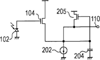
Fig. 1 is the block diagram according to the system of the first embodiment.Pel array 100 comprises N the pixel 101 of arranging one-dimensionally.Each pixel 101 comprises photodiode (PD) 102, reset transistor (Tr) 103, the first amplifier transistor (Tr) 104 and selects transistor (Tr) 105.In the present embodiment, each transistor is nmos pass transistor.Each transistor can be PMOS transistor or bipolar transistor in due course.
The first source follower circuit amplifies the signal corresponding with the amount of the signal charge that is produced by photoelectric conversion unit, and the output amplifying signal.In this manual, the signal corresponding with the amount of the signal charge that is produced by photoelectric conversion unit and be called as photoelectric conversion signal by making amplifying unit amplify the signal that this signal obtains.In the present embodiment, corresponding with the first amplifying signal according to the embodiment of the invention from the photoelectric conversion signal of the first source follower circuit output.
The first source follower circuit can be reset to output pixel noise signal in the state of resetting voltage at its voltage of inputting node.In this manual, the signal that the voltage with the input node in the state that is reset of voltage of input node is corresponding and be called as noise signal by making amplifying unit amplify the signal that this signal obtains.The state that the voltage of input node is reset comprises the state of Tr 103 conductings that reset that are connected with the input node and the state that is applied by the caused noise of the cut-off of the Tr103 that resets.After the Tr 103 that resets has ended, can change owing to the electric charge that produces by opto-electronic conversion the voltage of input node.Even in this case, the state as benchmark also can be to reset when calculating poor between photoelectric conversion signal and the noise signal.The state that is right after after Tr 103 cut-offs that reset is reset mode.In the present embodiment, corresponding with the 3rd amplifying signal according to the embodiment of the invention from the noise signal of the first source follower circuit output.Be output from output node OUT from the signal of pixel 101 output, and then be imported in the circuit at following stages place via output signal line 110.
Select Tr 105 between the active state of the first source follower circuit and inactive state, to switch.Node SEL is connected with the grid of selecting Tr 105, and strobe pulse pSEL is imported among the selection Tr 105.Select the operation of Tr 105 to be controlled by strobe pulse pSEL.
Column circuits module array 200 comprises a plurality of column circuits modules 201 that are connected with output signal line 110 respectively.Column circuits module array 200 is configured to parallel processing from the signal of a plurality of pixel outputs.Each column circuits module 201 comprises that current source 202, sampling keep (S/H) switch 203, intercondenser 204 and the second amplifier transistor (Tr) 205.
Second amplifies Tr 205 and current source 202 formation the second source follower circuit.The second source follower circuit amplifies from the photoelectric conversion signal of the first source follower circuit output, and exports this amplifying signal.Corresponding with the second amplifying signal according to the embodiment of the invention from the photoelectric conversion signal of the second source follower circuit output.In addition, the second source follower circuit can amplify the pixel noise signal, and exports the pixel noise signal of this amplification.Corresponding with the 4th amplifying signal according to the embodiment of the invention from the noise signal of the second source follower circuit output.
S/H switch 203 is disposed in as the output node OUT of the pixel 101 of the output node of the first source follower circuit and amplifies as second of the input node of the second source follower circuit on the path between the grid of Tr 205.S/H switch 203 can be arranged to direct connection output node OUT and be connected the grid that amplifies Tr 205 or the grid that connects output node OUT and the second amplification Tr 205 via other circuit element.By the S/H pulse that is input among the node pCM S/H switch 203 is switched between conducting state and cut-off state.Being electrically connected between the output node of S/H switch 203 control the first source follower circuit and the input node of the second source follower circuit.
Usually, amplifying circuit comprises at least one transistor and is used for to the bias supply of transistor supply bias current or bias voltage.The example that is used for the bias supply of supply bias current comprises current source.As making amplifying circuit enter the method for inactive state, can consider to be controlled at the transistorized bias state that comprises in the amplifying circuit so that method or the utilization of transistor cut-off are arranged in the method that the switch in the amplifying circuit makes amplifying circuit disconnect in electricity.For example, can make amplifying circuit enter inactive state by utilizing the path between the switch interrupts transistor AND gate bias supply.
Selected cell according to present embodiment can make the second source follower circuit enter inactive state when the first source follower circuit is in active state, and can make the first source follower circuit enter inactive state when the second source follower circuit is in active state.
Selected cell can make the first source follower circuit and source follower circuit enter simultaneously inactive state.For example, selected cell can make the first source follower circuit and the second source follower circuit enter inactive state by making selection Tr 105 enter not on-state and make S/H switch 203 enter conducting state.
Select each the transition ground (transitionally) between conducting state and not on-state in Tr 105 and the S/H switch 203 to switch.Therefore, during transition period, may uncertain the first source follower circuit and the second source follower circuit in which be in inactive state or the first source follower circuit and the second source follower and may be in active state.Selected cell can have can make the first amplifying unit and the second amplifying unit be in the configuration of above-mentioned state.
Arrange the memory cell 301 that is used for storage photoelectric conversion signal and noise signal for each output signal line 110 in due course.Storage array 300 comprises memory cell 301.Memory cell 301 comprises the holding capacitor (Cts) 313 for the storage photoelectric conversion signal, the holding capacitor (Ctn) 314 that is used for the storage noise signal, the Ct control switch 311 of sampling that is used for the signal of control Cts 313, the Ct control switch 312 of sampling that is used for the signal of control Ctn 314, be used for controlling to the horizontal sweep switch 315 of output of the signal of horizontal output line 402, and the horizontal sweep switch 316 of output that is used for controlling to the signal of horizontal output line 401. Ct control switch 311 and 312 is respectively by control signal pTS and pTN control. Horizontal sweep switch 315 and 316 is by the horizontal time-base hsr that produces by horizontal scanning circuit 500<1〉... or hsr<n (n represent row number) control.
Following stages place in horizontal output line 401 and 402 arrange to be used in due course output at the signal that outputs to horizontal output line 401 and to output to the output amplifier 600 of the difference between the signal of horizontal output line 402.By output in noise signal with comprise poor between the photoelectric conversion signal of the noise contribution relevant with the noise of pixel, can obtain with by signal corresponding to the clean quantity of electric charge of opto-electronic conversion generation.
Fig. 2 is the sequential chart that the operation of the circuit shown in Fig. 1 is shown.The pulse that has same reference numerals in Fig. 1 and Fig. 2 corresponds to each other.With reference to figure 2, transverse axis represents the time.Describe the operation of the system shown in Fig. 1 in detail with reference to the sequential chart shown in Fig. 2.When each pulse is in high level, inductive switch is switched on.Suppose that accumulating the signal that obtains in the period in last time is stored in the memory cell 301.
In period RESET1, the pulse of the level of the switch conduction corresponding with node R ES, SEL and pCM is input to respectively among node R ES, SEL and the pCM.The Tr 103 that resets after pulse has been input among the node R ES enters conducting state, so that the electromotive force of PD 102 and the first electromotive force (that is, the electromotive force of the input node of the first source follower circuit) that amplifies the grid of Tr 104 are reset.
Fig. 5 A is the figure by the circuit in the zone 50 of the dashed line encirclement that replaces that illustrates among Fig. 1.Fig. 5 B is the figure that is illustrated in the connection status of the circuit shown in Fig. 5 A among the period RESET1.With reference to figure 5B, when being in conducting state (conduction state) when switch or as the transistor of switch, by switch or transistor two node solid line short circuits connected to one another.When being in cut-off state (non-conductive state) when switch or as the transistor of switch, by not having solid line between switch or transistor two nodes connected to one another.Therefore, in Fig. 5 B and other accompanying drawing, simplified the expression of circuit.
With reference to figure 5B, the second grid voltage that amplifies Tr 205 is identical with source voltage.Therefore, second amplifies the output that Tr 205 is in cut-off state and does not affect pixel.That is, the second source follower circuit is not carried out amplifieroperation and is in inactive state.On the other hand, comprise that the first the first source follower circuit that amplifies Tr 104 is in active state.The first source follower circuit amplifies and is applied to as signal corresponding to the resetting voltage of the grid of the first amplification Tr 104 of the importation of the first source follower circuit, and this amplifying signal is outputed to output signal line 110.
Among the period RES_SH1, the pulse of the level of Tr 103 cut-offs that reset is imported among the node R ES shown in figure 2.The cut-off of Tr 103 of resetting produces noise contribution and this noise contribution is superimposed on the resetting voltage.Be sampled intercondenser 204 from the noise signal of the first source follower circuit output.In the present embodiment, after the period, RES_SH1 passed, beginning light was accumulated the period.
Fig. 5 C is illustrated in the connection status of the circuit shown in Fig. 5 A among the period RES_SH1.In this period, the first source follower circuit also is in active state, and the second source follower circuit also is in inactive state.
In period HSCAN1, the pulse of the level of the switch cut-off corresponding with node SEL and pCM is input to respectively among node SEL and the pCM.In this period, in response to horizontal time-base hsr<1〉... or hsr<n, will accumulate the photoelectric conversion signal and the noise signal that are stored in respectively in the period among Cts 313 and the Ctn 314 at light last time and export to the outside from output amplifier 600 via horizontal output line 402 and 401 respectively.
Fig. 5 D is the figure that is illustrated in the connection status of the circuit shown in Fig. 5 A among the period HSCAN1.With reference to figure 5D, S/H switch 203 is in cut-off state, and the second source electrode that amplifies Tr 205 is not connected with grid to connect.Here, can make second to amplify Tr 205 and operate in level in the saturation region by being set as by the level of the first source follower circuit amplifying signal, make second to amplify Tr 205 conductings.That is, the second source follower circuit enters active state, receives the noise signal that is stored in the intercondenser 204, amplifies noise signal, and the noise signal of amplifying is outputed to output signal line 110.On the other hand, owing to select Tr 105 to make first to amplify Tr 104 and current source 202 and disconnect in electricity, therefore the first source follower circuit is in inactive state.
In period SHN, the pulse of the level of Ct control switch 312 conductings is imported among the node pTN.In this period, the connection status of the circuit shown in Fig. 5 A is shown in Fig. 5 D.Comprise that the second the second source follower circuit that amplifies Tr 205 and current source 202 amplifies the noise signal that is stored in the intercondenser 204, and in Ctn 314, amplifying signal is sampled.
After noise signal is sampled in Ctn 314, the pulse of the level of the switch conduction corresponding with node SEL and pCM is input to respectively among node SEL and the pCM.In period LIGHT_SH, as among the period RES_SH1, the connection status of the circuit shown in Fig. 5 A is shown in Fig. 5 C.That is, the second source follower circuit is in inactive state, and the first source follower circuit is in active state.The photoelectric conversion signal that is amplified by the first source follower circuit is sampled in intercondenser 204.After the period, LIGHT_SH passed, light was accumulated the period end.
In period SHS, the pulse of the level of the switch cut-off corresponding with node SEL and pCM is input to respectively among node SEL and the pCM, and the pulse of the level of Ct control switch 311 conductings is imported among the node pTS.At that time, the connection status of the circuit shown in Fig. 5 A is shown in Fig. 5 D.That is, the second source follower circuit is in active state, and photoelectric conversion signal is sampled in Cts 313.
In period RESET2 and RES_SH2, carry out reset operation and noise signal sampling operation.In period HSCAN2, read out in the noise signal of the photoelectric conversion signal of sampling among the Cts 313 and sampling in Ctn 314.
Separately control inputs in the node pSEL pulse and be input to pulse among the node pCM.Therefore, can in the situation of the conducting state of not considering other source follower circuit, control in the first source follower circuit and the second source follower circuit each active state and the switching between the inactive state.Can utilize the control impuls of the timing generator transmission from be arranged in solid-state image pickup apparatus or the control impuls that sends from outsides such as CPU to realize this control.
As previously described, in the present embodiment, when when carrying out sampling processing such as the capacitor of intercondenser 204, Cts 313 or Ctn 314, the first source follower circuit or the second source follower circuit are in active state.Especially, when being sampled in amplifying signal is being arranged in the signal memory cell (intercondenser 204 or memory cell 301) at level place of each source follower circuit back, these two source follower circuits are not in active state.As a result, the first amplification Tr 104 and the second amplification Tr 205 can share current source 202 and not increase power consumption.According to present embodiment, compared with prior art, can reduce the quantity of current source.This is so that the power consumption minimizing.
In the present embodiment, can be by realizing the quantity of sharing to reduce required element of current source.This is so that the size reduction of solid-state image pickup device.
In the present embodiment, the output node of the first source follower circuit is connected with output signal line 110 with the output node of the second source follower circuit.Output signal line 110 is connected with current source 202.Use this configuration, can reduce the quantity of the circuit in the circuit.This is so that the size reduction of solid-state image pickup device.
In the present embodiment, memory cell 301 comprises Cts 313 and Ctn 314.Use this configuration, photoelectric conversion signal can be stored among the Cts 313, and noise signal can be stored among the Ctn 314, and can be from poor between photoelectric conversion signal and noise signal of output amplifier 600 output.Therefore can reduce the noise that the variation by the transistor characteristic in the pixel causes.
In the present embodiment, as substituting of noise signal and photoelectric conversion signal, the signal that is relative to each other aspect pixel resets can be imported in the output amplifier 600.Because poor between these signals of output amplifier 600 output, the pixel reset noise that therefore comprises in the signal of output amplifier 600 outputs reduces.Use this configuration, can catch high-quality and low noise image.
In the present embodiment, selecting Tr 105 to be connected with output signal line with the first amplification Tr 104 is connected.Yet, for example, select Tr 105 can and power line and first amplify Path Connection between the drain electrode of Tr 104.
The supply voltage that is used for the first source follower circuit and the second source follower circuit is not necessarily identical, and can differ from one another, thus so that these circuit executable operations in opereating specification effectively.
In the present embodiment, pixel 101 can have diffusion of floating (FD) unit at PD 102 and the first Nodes that amplifies between the Tr 104.In the present embodiment, the configuration of reading circuit that is arranged in the level place of linear memory back is not limited to the configuration shown in Fig. 1.For example, the level place in column circuits module array 200 back can arrange amplifying circuit or analog to digital converter (ADC) such as the switched capacitor amplifier.
The second embodiment
Fig. 3 is the block diagram according to the system of the second embodiment.Identical Reference numeral is used to be identified at the parts of having described among the first embodiment, and therefore with the descriptions thereof are omitted.With the difference of describing between the first embodiment and the second embodiment.
In the present embodiment, pixel 101 comprises PD 102, Tr 103 and be included in first in the first source follower circuit and amplify Tr 104 resets.Difference between the second embodiment and the first embodiment is that pixel 101 does not comprise selection Tr 105.
Not shown in Fig. 3 at the circuit that the level of column circuits module array 200 back is located.With the level place that can be disposed in column circuits module array 200 back according to the similar circuit of the circuit of the first embodiment or circuit of the prior art.
As described in detail later, DAC 700 makes the first source follower circuit enter inactive state, and S/H switch 203 makes the second source follower circuit enter inactive state.In the present embodiment, S/H switch 203 and DAC 700 are corresponding with selected cell according to the embodiment of the invention.
Fig. 4 is the sequential chart that the operation of the circuit shown in Fig. 3 is shown.Describe the operation of the circuit shown in Fig. 3 in detail with reference to the sequential chart shown in Fig. 4.
With reference to figure 4, in period RESET1, PD 102 is reset.Fig. 6 A is the figure by the circuit in the zone 50 of the dashed line encirclement that replaces that illustrates among Fig. 3.In period RESET1, the connection status of the circuit shown in Fig. 6 A is shown in Fig. 6 B.With reference to figure 6B, when being in conducting state (conduction state) when switch or as the transistor of switch, by switch or transistor two node solid line short circuits connected to one another.When being in cut-off state (non-conductive state) when switch or as the transistor of switch, by not having solid line between switch or transistor two nodes connected to one another.Therefore, in Fig. 6 B and other accompanying drawing, simplified the expression of circuit.
With reference to figure 6B, the second grid voltage that amplifies Tr 205 is identical with source voltage.Therefore, second amplifies Tr 205 is in cut-off state, and the second source follower circuit is in inactive state.On the other hand, first amplifies Tr 104 is in conducting state, and the first source follower circuit is in active state.The first source follower circuit amplifies the signal corresponding with the resetting voltage of the grid that is applied to the first amplification Tr 104, and amplifying signal is outputed to output signal line 110.At that time, DAC 700 is to node VSEL supply GND electromotive force.
In period RES_SH1, noise signal is sampled in intercondenser 204.Fig. 6 C is the figure that is illustrated in the connection status of the circuit shown in Fig. 6 A among the period RES_SH1.In this period, second amplifies Tr 205 also is in cut-off state, and the first amplification Tr 104 also is in conducting state.That is, the first source follower circuit is in active state, and the second source follower circuit is in inactive state.Because therefore DAC 700 samples to noise signal take the GND electromotive force as benchmark in intercondenser 204 to node VSEL supply GND electromotive force.
In period HSCAN1, electric charge is accumulated in the photoelectric conversion unit.Fig. 6 D is the figure that is illustrated in the connection status of the circuit shown in Fig. 6 A among the period HSCAN1.In Fig. 6 D, VPD represents that first amplifies the grid potential of Tr 104, and VCM represents that second amplifies the grid potential of Tr 205.Among the period HSCAN1 shown in Figure 4, DAC 700 is to node VSEL output reference voltage VSEL_L.Even VPD is because the electric charge that produces by opto-electronic conversion descends, reference voltage VSEL_L has also kept the relation of VPD>VCM.Therefore the voltage of output signal line 110 becomes the voltage corresponding with the grid voltage of the first amplification Tr 104.Because the second grid voltage that amplifies Tr 205 is lower than the source voltage of the second amplification Tr 205, therefore the second amplification Tr 205 is in cut-off state.That is, as among the period RES_SH1, the second source follower circuit is in inactive state and the first source follower circuit is in active state.
In period SHN, DAC 700 utilizes this reference voltage VSEL_H to keep the relation of VPD<VCM to node VSEL output reference voltage VSEL H.Fig. 6 E is the figure that is illustrated in the connection status of the circuit shown in Fig. 6 A among the period SHN.In Fig. 6 E, owing to keep the relation of VPD<VCM, therefore the voltage corresponding with the grid voltage of the second amplification Tr 205 is output to output signal line 110.Because the first source voltage that amplifies Tr 104 is higher than the grid voltage of the first amplification Tr 104, therefore the first amplification Tr 104 is in cut-off state.Therefore, comprise that the second the second source follower circuit that amplifies Tr 205 and current source 202 amplifies the noise signal that is stored in the intercondenser 204, and the noise signal of output amplification.
In period LIGHT_SH, photoelectric conversion signal is sampled in intercondenser 204.At that time, as among the period RES_SH1, the connection status of the circuit shown in Fig. 6 A is shown in Fig. 6 C.That is, the second amplification Tr 205 is in cut-off state.
In period SHS, DAC 700 utilizes this reference voltage VSEL_H to keep the relation of VPD<VCM to node VSEL output reference voltage VSEL_H.The connection status of the circuit shown in Fig. 6 A is again shown in Fig. 6 E.Be switched on because second amplifies Tr 205, therefore the second source follower circuit enters active state and the photoelectric conversion signal that is stored in the intercondenser 204 is output.
When the second source follower circuit output photoelectric switching signal and noise signal, the reference voltage VSEL_H that DAC700 output is identical.Therefore, determine the signal value of photoelectric conversion signal and noise signal take identical reference voltage as benchmark.
In period RESET2 and RES_SH2, carry out reset operation and noise signal sampling operation.
As previously described, in the present embodiment, be used for the reference potential of intercondenser 204 by control, when carry out sampling operations at intercondenser 204 and be stored in signal in the intercondenser 204 when being output the first source follower circuit or the second source follower circuit be in active state.Therefore, can amplify Tr 104 and second by first and amplify Tr 205 shared current sources 202, and can reduce the quantity of current source.This is so that the power consumption minimizing.
In the present embodiment, owing to do not need to select Tr 105, therefore can reduce the transistorized quantity in the pixel.Therefore can suppress to be reduced by the area of photoelectric conversion unit the impact of the sensitivity of caused photoelectric conversion unit.
In the present embodiment, use DAC 700 as the reference voltage output circuit for generation of the reference voltage that will be supplied to node VSEL.Yet, for example, can use the circuit that can use a plurality of switches to select the voltage of expectation.
In the present embodiment, the reference potential transition ground that is used for intercondenser 204 changes, thus first amplify Tr 104 and second amplify among the Tr 205 each conducting state and cut-off state between switch.Yet, for example, for first amplify Tr 104 and second amplify among the Tr 205 each conducting state and cut-off state between switch, being applied to the first value of voltage of amplifying the grid of Tr 104 can be by the control of transition ground, and perhaps first amplifies Tr 104 or the second drain voltage that amplifies Tr 205 can be controlled.
Changed by transition ground owing to be used for the reference potential of intercondenser 204, therefore the first source follower circuit and the second source follower circuit can temporarily be in active state.Selected cell can have the configuration that can make the first amplifying unit and the second amplifying unit enter above-mentioned state.
The 3rd embodiment
Fig. 7 is the block diagram according to the system of the 3rd embodiment.Identical Reference numeral is used to be identified at the parts of having described among the first embodiment, and therefore with the descriptions thereof are omitted.
Difference between the 3rd embodiment and the first embodiment is the configuration of pixel 101.The first grid that amplifies Tr 104 is connected with the diffusion (FD) 106 of floating.Transfering transistor (Tr) 107 is disposed between PD 102 and the FD 106.
Node TX is connected with the grid that shifts Tr 107, and transfer pulse pTX is imported among the transfer Tr 107.Shift the operation of Tr 107 by shifting pulse pTX control.When transfer Tr 107 enters conducting state, be stored in the depleted FD106 of transferring to of electric charge among the PD 102.Electric charge will be exhausted fully from PD 102 transfers to FD 106.
Row amplifying unit 901 is disposed between column circuits module 201 and the memory cell 301.Column amplifier array 900 comprises N the row amplifying unit 901 of arranging one-dimensionally.Each row amplifying unit 901 comprises clamp (clamp) capacitor 902, feedback condenser 903, reset switch 904 and operational amplifier 905.
One end of clamping capacitance device 902 is connected with output signal line 110, and the other end of clamping capacitance device 902 is connected with the paraphase input node of operational amplifier 905.One end of feedback condenser 903 is connected with the paraphase of operational amplifier 905 input node, and the other end of feedback condenser 903 is connected with the output node of operational amplifier 905.Reset switch 904 is arranged such that it is in parallel with feedback condenser 903.Reset switch 904 is by the pulse control that is input among the node pC0R.The noninvert input node of operational amplifier 905 is connected with the GND electromotive force.
In the circuit shown in Figure 7, feedback condenser 903 is only formed by a capacitor.Yet, in feedback condenser 903, can arrange a plurality of capacitors with being connected in parallel to each other, and can arrange the switch that is connected with each capacitor's seriesu.Multiple unit capacitor and switch can switch between the gain in row amplifying unit 901 by in feedback condenser 903, arranging with being connected in parallel to each other.
Although not shown, except current source 202, also arranged the current source that is used for to operational amplifier 905 supply bias currents.That is, operational amplifier 905 not with the first source follower circuit and the shared current source of the second source follower circuit.Operational amplifier 905 is corresponding to the 3rd amplifying unit according to the embodiment of the invention.
Fig. 8 is the sequential chart that the operation of the circuit shown in Fig. 7 is shown.Describe the operation of the circuit shown in Fig. 7 in detail with reference to the sequential chart shown in Fig. 8.When each pulse is in high level, inductive switch is switched on.Suppose that PD 102 has carried out light and accumulated.
With reference to figure 8, in the period between t0 and t1, the pulse of the level of corresponding transistor turns is input to respectively among node R ES, SEL, pCM and the pC0R.As a result, the electromotive force of FD 106 is reset.
In period between t1 and t2, the pulse of the level of Tr 103 cut-offs that reset is imported among the node R ES.Be superimposed on resetting voltage for FD 106 by the caused noise contribution of cut-off of the Tr 103 that resets.At that time, the noise signal from the output of the first source follower circuit is sampled intercondenser 204.Because the source electrode of the second source follower circuit and grid are by short circuit, therefore the second source follower circuit is in inactive state.
In period between t2 and t3, the pulse of the level of corresponding transistor cut-off is input to respectively among node SEL and the pCM.As a result, the second source follower circuit enters active state.Be stored in that noise signal in the intercondenser 204 is amplified by the second source follower circuit and then by sampling in clamping capacitance device 902.Because select Tr 105 to be in cut-off state, therefore the first source follower circuit is in inactive state.
In period between t4 and t5, the pulse of the level of Ct control switch 312 conductings is imported among the node pTN.As a result, noise signal is stored among the Ctn 314.
In period between t6 and t7, the pulse of the level of corresponding switch conduction is input to respectively among node TX, SEL and the pCM.Because make transfer Tr 107 enter conduction, the signal charge that therefore is stored among the PD 102 is transferred to FD 106.After this period passed, light was accumulated the period end.
In period between t7 and t8, shift Tr 107 cut-offs, and the photoelectric conversion signal corresponding with the amount of the electric charge of transferring to FD106 is sampled in intercondenser 204.At that time, the first source follower circuit is in active state, and the second source follower circuit is in inactive state.
In period between t8 and t9, the pulse of the level that inductive switch is ended is input to respectively among node SEL and the pCM.As a result, the second source follower circuit enters active state, and is stored in the clamping capacitance device 902 in noise signal and the difference that is stored between the photoelectric conversion signal in the intercondenser 204.
In period between t9 and t10, the pulse of the level of Ct control switch 311 conductings is imported among the node pTS.As a result, photoelectric conversion signal is sampled in Cts 313.
In period between t11 and t12, the pulse of the level of corresponding transistor turns is input to respectively among node TX and the RES.As a result, reset Tr 103 and transfer Tr 107 enter conducting, and the electromotive force of PD 102 and FD 106 is reset.The pulse of the level that shifts Tr 107 cut-offs is imported among the node TX, and light is accumulated the period and is begun.
In period between t13 and t14, the noise signal of the photoelectric conversion signal of sampling and sampling in Ctn 314 is sent to respectively horizontal output line 402 and 401 in Cts 313.Difference between photoelectric conversion signal and noise signal is obtained by output amplifier 600 and exports from output amplifier 600.
In the present embodiment, when the second source follower circuit will be stored in noise signal in the intercondenser when writing in the clamping capacitance device 902, the enlarging function that uses the operational amplifier 905 in the row amplifying unit 901 is set as the GND electromotive force with the node in operational amplifier 905 1 sides of clamping capacitance device 902.Therefore, operation amplifier when signal is clamped in the clamping capacitance device.That is, in the present embodiment, row amplifying unit 901 when the first source follower circuit or the second source follower circuit are in active state operation as amplifying circuit.Therefore, the operational amplifier 905 that is included in the row amplifying unit 901 is not shared current source with the first source follower circuit and the second source follower circuit.
In the present embodiment, except the effect that in the first embodiment, can obtain, can also obtain following effect.In the present embodiment, pixel 101 comprises transfer Tr 107.Owing to shift Tr 107 PD 102 and FD 106 are disconnected in electricity, so PD 102 can be maintained at the electromotive force of FD 106 in the state of reset potential and accumulate light.Use this configuration, can reduce the sampling of noise signal in intercondenser 204 and the time interval between the sampling of photoelectric conversion signal in intercondenser 204.This is so that the impact minimizing of 1/f noise.
System according to present embodiment comprises row amplifying unit 901, and this row amplifying unit 901 comprises clamping capacitance device 902.Use this configuration, can reduce the caused noise of variation by the characteristic of pixel 101 and column circuits module 201.
In the present embodiment, memory cell 301 is disposed in the level place of row amplifying unit 901 back.Use this configuration, can reduce the caused noise of variation by the characteristic of row amplifying unit 901.
The exemplary variation of the 3rd embodiment
Fig. 9 is the figure that illustrates according to the exemplary variation of the system of the 3rd embodiment.Identical Reference numeral is used to be identified at the parts of having described among the 3rd embodiment, and therefore with the descriptions thereof are omitted.
Pel array 100R, 100G and 100B are arranged to three row.For example, respectively output and ruddiness, green glow, signal that blue light is corresponding of pel array 100R, 100G and 100B.In Fig. 9, only show three pixels in single-row, i.e. pixel 101R, 101G and 101B.Yet, thereby can arrange parallel the reading of a plurality of pixel columns realizations.
For each pixel arrangement column circuits module 201 and clamping capacitance device 902.Correspondence between pixel and the assembly is represented by R, G or the B at digital end.Column circuits module 201 can be by some pixel sharings.For example, column circuits module 201 can be shared by the pixel 101M that catches for monochrome image and the pixel 101R corresponding with ruddiness.
Reset Tr 103R, 103G and 103B in the pixel are by common pulse control.Selection Tr in the pixel is similarly by common pulse control.Transfer Tr in the pixel is similarly by common pulse control.Controlled by common pulse like the S/H Switch in the column circuits module.
Row amplify on the path between inverting terminal that switch 906R, 906G and 906B be arranged in clamping capacitance device 902R, 902G and 902B and operational amplifier 905.Row amplify the conduction state of switch 906R, 906G and 906B respectively by pulse psw_r, psw_g and psw_b control.
Figure 10 is the sequential chart that the operation of the circuit shown in Fig. 9 is shown.Describe the operation of the circuit shown in Fig. 9 in detail with reference to the sequential chart shown in Figure 10.Supposing to have begun in photoelectric conversion unit light accumulates.
Be cut off and after noise signal has been written in the intercondenser at the Tr that resets, made the pulse of the level of corresponding switch conduction be input to respectively row and amplify among switch 906R, 906G and the 906B.The noise signal that writes the pixel in the intercondenser is clamped at respectively in the clamping capacitance device simultaneously.At that time, the electromotive force at the node of operational amplifier 905 1 sides of clamping capacitance device is set to the GND electromotive force.
After reset switch 904 has ended, the pulse of the level of Ct control switch 312 conductings is transfused to, and the skew composition of operational amplifier 905 (offset component) is written among the Ctn 314.
The pulse of the level that shifts the Tr conducting is imported among the node TX, and accumulates the signal charge that in pixel, produces in the period at light and transferred to respectively FD simultaneously.When shifting the Tr cut-off, light is accumulated the period end.
After signal charge was transferred to FD, the pulse psw_r that makes row amplify the level of switch 906R conducting was transfused to.As a result, the photoelectric conversion signal of pixel 101R is clamped among the clamping capacitance device 902R.Subsequently, the pulse of the level of Ct control switch 311 conductings is transfused to, and the photoelectric conversion signal of pixel 101R is written among the Cts 313.The signal that writes among Cts313 and the Ctn 314 is sent to respectively the horizontal output line.Output amplifier 600 outputs do not comprise the signal of the skew composition of column amplifier.
Subsequently, the pulse of the level of reset switch 904 conductings is transfused to, and the electromotive force of the output node of operational amplifier 905 is set to the GND electromotive force.After operational amplifier 905 has been reset, the pulse of the level of Ct control switch 312 conductings is transfused to and the skew composition of operational amplifier 905 is written among the Ctn 314.
Subsequently, the pulse psw_g that makes row amplify the level of switch 906G conducting is transfused to.As a result, the photoelectric conversion signal of pixel 101G is clamped among the clamping capacitance device 902G.Subsequently, Ct control switch 311 enters conducting, and the photoelectric conversion signal of pixel 101G is written among the Cts 313.Signal is sent to respectively the horizontal output line, and output amplifier 600 obtains poor between these signals.
After the skew composition of operational amplifier 905 had been read, the same as the photoelectric conversion signal of pixel 101R and 101G, the photoelectric conversion signal of pixel 101B was read.
Except the effect that in the 3rd embodiment, can obtain, can also obtain following effect.In this exemplary variation of the 3rd embodiment, after all pixels were resetted simultaneously, the photoelectric conversion signal of these pixels can be write in the intercondenser respectively simultaneously.Use this configuration, even pixel is arranged on and also can sets identical light in all pixels in a plurality of row and accumulate the period.
The 4th embodiment
Figure 11 is the block diagram according to the system of the 4th embodiment.Identical Reference numeral is used to be identified at the parts of having described among the first to the 3rd embodiment, and therefore with the descriptions thereof are omitted.
In the present embodiment, arrange that voltage follower circuit replaces the second source follower circuit according to the first embodiment.More particularly, arrange that the differential amplifier circuit that comprises 211 and 212 and two nmos pass transistors of two PMOS transistors (Tr) (Tr) 213 and 214 replaces amplifying Tr 205 according to second of the first embodiment.PMOS Tr 211 and 212, NMOS Tr 213 and 214 and current source 202 form operational amplifiers 210.
When S/H switch 203 was in conducting state, the grid of NMOS Tr 214 was identical with the electromotive force of source electrode.Owing to do not have electric current to pass through operational amplifier 210, so voltage follower circuit is in inactive state.When selecting Tr 105 to be in conducting state, the first source follower circuit that is in active state amplifies the signal of pixel, and amplifying signal is outputed to intercondenser 204.
When selecting Tr 105 and S/H switch 203 to be in cut-off state, the first source follower circuit is in inactive state.On the other hand, the voltage follower circuit that is in active state amplifies the signal that is stored in the intercondenser 204, and the output amplifying signal.When selecting Tr 105 and 203 cut-off of S/H switch, S/H switch 203 at first ends.
In the present embodiment, select Tr 105 and S/H switch 203 corresponding with selected cell according to the embodiment of the invention.
In the present embodiment, voltage follower circuit is used as the second amplifying unit.Use this configuration, except the effect that in the first embodiment, can obtain, can also obtain following effect.The gain of the voltage follower circuit of use operational amplifier is close to 1.Therefore, can improve the linear relationship between the input and output, and realize the image capture of high quality graphic.
In the present embodiment, can use configuration according to the second embodiment or the 3rd embodiment.
The 5th embodiment
Figure 12 is the block diagram according to the system of the 5th embodiment.Identical Reference numeral is used to be identified at the parts of having described among the first to the 4th embodiment, and therefore with the descriptions thereof are omitted.
Difference between the 5th embodiment and the first embodiment is, arranges that respectively the first voltage follower circuit and second voltage follower circuit replace the first source follower circuit and the second source follower circuit.Layout comprises the first differential amplifier circuit of two PMOS transistors 111 and 112 and two nmos pass transistors 113 and 114, replaces first in the pixel 101 to amplify Tr 104.The first differential amplifier circuit is via selecting Tr 105 to be connected with current source 202.The first differential amplifier circuit and current source 202 form the first voltage follower circuit.
Comprise PMOS Tr 211 with are connected and NMOS Tr 213 and second differential amplifier circuit of being connected via selecting transistor (Tr) 215 to be connected with current source 202.The second differential amplifier circuit and current source 202 form the second voltage follower circuit.
In the present embodiment, by between the conducting state of selecting Tr 105 and cut-off state, switching to carry out in the active state of the first voltage follower circuit and the switching between the inactive state, and by between the conducting state of selecting Tr 215 and cut-off state, switching to carry out in the active state of second voltage follower circuit and the switching between the inactive state.Select Tr 105 and 215 corresponding with selected cell according to the embodiment of the invention.
Use this configuration, can further improve the linear relationship between the input and output, because two amplifying units are formed by voltage follower circuit respectively.This is so that the picture quality raising.
In the 4th embodiment and the 5th embodiment, use the voltage follower circuit that comprises operational amplifier.Yet, can replace voltage follower circuit than 1 high amplifying circuit with voltage gain.
In the first to the 5th embodiment, electronics is equivalent to signal charge.Yet the hole can be equivalent to signal charge.In this case, the polarity of PD 102 and each transistorized conduction type are inverted.For example, in a second embodiment, even use the opposite polarity photodiode of the PD 102 shown in its polarity and Fig. 3, also can come by the voltage conditions of knot modification VSEL the change of response light electric diode.
In the first to the 5th embodiment, signal is amplified by the amplifying unit of two-stage.Yet signal can be amplified by the amplifying unit more than two-stage in due course, and current source can be shared by these amplifying units.
In the first to the 5th embodiment, for the purpose of simplifying the description, the line sensor of the pel array with 1 row N row has been described.Yet embodiments of the invention can be applied to having the face sensor of two-dimentional pel array.
Although reference example embodiment has described the present invention, should be appreciated that to the invention is not restricted to disclosed exemplary embodiment.Thereby the scope of following claim will be given the widest explanation comprises all such modifications, the structure that is equal to and function.
Claims (20)
1. solid-state image pickup apparatus comprises:
Converting unit is configured to produce electric charge;
The first amplifying unit is configured to amplify the signal corresponding with the amount of electric charge and exports the first amplifying signal;
The second amplifying unit is configured to amplify the first amplifying signal and exports the second amplifying signal;
Current source is shared by the first amplifying unit and the second amplifying unit; And
Selected cell is configured to make individually the first amplifying unit and the second amplifying unit to enter inactive state.
2. solid-state image pickup apparatus according to claim 1 also comprises:
Switch element is configured to be controlled at the electrical connection between the second input node of the first output node of the first amplifying unit and the second amplifying unit; And
Memory cell is disposed on switch element and the second path of input between the node, and is configured to store the first amplifying signal or based on the signal of the first amplifying signal.
3. solid-state image pickup apparatus according to claim 2 also comprises output signal line, and
Wherein the first output node is electrically connected with output signal line,
Wherein output signal line is electrically connected with the second input node via switch element,
Wherein the second output node of the second amplifying unit is electrically connected with output signal line, and
Wherein current source is electrically connected with output signal line.
4. solid-state image pickup apparatus according to claim 3 also comprises the power line that is configured to the first amplifying unit supply bias voltage, and
Wherein the first amplifying unit comprises the first amplifying mos transistor,
Wherein the first grid of the first amplifying mos transistor is the first input node of the first amplifying unit, and the first source electrode of the first amplifying mos transistor is the first output node, and the first drain electrode of the first amplifying mos transistor is electrically connected with power line, and
Wherein select transistor be disposed in first the drain electrode and power line between the path or on the path between the first source electrode and the output signal line.
5. solid-state image pickup apparatus according to claim 1 also comprises the output circuit that is configured to export a plurality of reference voltages, and
Wherein the first amplifying unit comprises the first amplifier transistor,
Wherein the second amplifying unit comprises the second amplifier transistor, and
Wherein output circuit is controlled at least one the bias state in the first amplifier transistor and the second amplifier transistor.
6. solid-state image pickup apparatus according to claim 1 also comprises:
Reset unit, the voltage of the first input Nodes of first amplifying unit that is configured to reset; And
The difference operation unit, and
Wherein the first amplifying unit is amplified in the signal corresponding with the voltage of the first input Nodes in the first state of being reset of input node, and exports the 3rd amplifying signal,
Wherein the second amplifying unit amplifies the 3rd amplifying signal and exports the 4th amplifying signal, and
Wherein the difference operation unit be configured to export with the second amplifying signal and the 4th amplifying signal between poor corresponding difference signal.
7. solid-state image pickup apparatus according to claim 6, wherein the second amplifying signal and the 4th amplifying signal comprise the noise contribution that is relative to each other.
8. solid-state image pickup apparatus according to claim 1 also comprises:
The diffusion of floating that is electrically connected with the first input node of the first amplifying unit; And
Buanch unit is configured to electric charge is transferred to the diffusion of floating.
9. solid-state image pickup apparatus according to claim 1 also comprises many group converting units, the first amplifying unit, the second amplifying unit and current source.
10. solid-state image pickup apparatus according to claim 1 also is included in the 3rd amplifying unit at the level place of the second amplifying unit back, and
Wherein the 3rd amplifying unit is not shared current source with the first amplifying unit and the second amplifying unit.
11. solid-state image pickup apparatus according to claim 1, wherein selected cell makes the first amplifying unit and the second amplifying unit enter simultaneously inactive state.
12. solid-state image pickup apparatus according to claim 1, wherein the first amplifying unit and the second amplifying unit are source follower circuits.
13. a method that is used for the driving of solid-state image pickup apparatus, described solid-state image pickup apparatus comprises: converting unit is configured to produce electric charge; The first amplifying unit is configured to amplify the signal corresponding with the amount of electric charge and exports the first amplifying signal; The second amplifying unit is configured to amplify the first amplifying signal and exports the second amplifying signal; Current source is shared by the first amplifying unit and the second amplifying unit; And selected cell, be configured to make the first amplifying unit and the second amplifying unit to enter inactive state, described method comprises the steps:
When being in active state, the first amplifying unit make the second amplifying unit enter inactive state; And
When being in active state, the second amplifying unit make the first amplifying unit enter inactive state.
14. method according to claim 13, wherein said solid-state image pickup apparatus also comprises:
Switch element is configured to be controlled at the electrical connection between the second input node of the first output node of the first amplifying unit and the second amplifying unit; And
Memory cell is disposed on switch element and the second path of input between the node, and is configured to store the first amplifying signal or based on the signal of the first amplifying signal.
15. method according to claim 14, wherein said solid-state image pickup apparatus also comprises output signal line,
Wherein the first output node is electrically connected with output signal line,
Wherein output signal line is electrically connected with the second input node via switch element,
Wherein the second output node of the second amplifying unit is electrically connected with output signal line, and
Wherein current source is electrically connected with output signal line.
16. method according to claim 15,
Wherein said solid-state image pickup apparatus also comprises the power line that is configured to the first amplifying unit supply bias voltage,
Wherein the first amplifying unit comprises the first amplifying mos transistor,
Wherein the first grid of the first amplifying mos transistor is the first input node of the first amplifying unit, and the first source electrode of the first amplifying mos transistor is the first output node, and the first drain electrode of the first amplifying mos transistor is electrically connected with power line, and
Wherein select transistor be disposed in first the drain electrode and power line between the path or on the path between the first source electrode and the output signal line.
17. method according to claim 13,
Wherein said solid-state image pickup apparatus also comprises the output circuit that is configured to export a plurality of reference voltages,
Wherein the first amplifying unit comprises the first amplifier transistor,
Wherein the second amplifying unit comprises the second amplifier transistor, and
Wherein output circuit is controlled at least one the bias state in the first amplifier transistor and the second amplifier transistor.
18. method according to claim 13, wherein said solid-state image pickup apparatus also comprises:
Reset unit, the voltage of the first input Nodes of first amplifying unit that is configured to reset; And
The difference operation unit,
Wherein the first amplifying unit is amplified in the signal corresponding with the voltage of the first input Nodes in the first state of being reset of input node, and exports the 3rd amplifying signal,
Wherein the second amplifying unit amplifies the 3rd amplifying signal and exports the 4th amplifying signal, and
Wherein the difference operation unit be configured to export with the second amplifying signal and the 4th amplifying signal between poor corresponding difference signal.
19. method according to claim 13, wherein said solid-state image pickup apparatus also comprises:
The diffusion of floating that is electrically connected with the first input node; And
Buanch unit is configured to electric charge is transferred to the diffusion of floating.
20. a method that is used for the driving of solid-state image pickup apparatus, described solid-state image pickup apparatus comprises: converting unit is configured to produce electric charge; The first amplifying unit is configured to amplify the signal corresponding with the amount of electric charge and exports the first amplifying signal; The second amplifying unit is configured to amplify the first amplifying signal and exports the second amplifying signal; Current source is shared by the first amplifying unit and the second amplifying unit; Be included in the first amplifying mos transistor in the first amplifying unit; Output signal line; Switch element; And selection transistor, output signal line is electrically connected via the source electrode of selecting transistor AND gate the first amplifying mos transistor, switch element is configured to control the second electrical connection of inputting between the node of output signal line and the second amplifying unit, the second output node of the second amplifying unit is connected with output signal line, current source is connected with output signal line, and described method comprises the steps:
When the first amplifying unit is in active state by making the switch element conducting make the second amplifying unit enter inactive state; And
When being in active state, the second amplifying unit select transistor to end to make the first amplifying unit to enter inactive state by making.
Applications Claiming Priority (2)
| Application Number | Priority Date | Filing Date | Title |
|---|---|---|---|
| JP2010-039070 | 2010-02-24 | ||
| JP2010039070A JP5506450B2 (en) | 2010-02-24 | 2010-02-24 | Solid-state imaging device and driving method of solid-state imaging device |
Publications (2)
| Publication Number | Publication Date |
|---|---|
| CN102164252A CN102164252A (en) | 2011-08-24 |
| CN102164252B true CN102164252B (en) | 2013-10-30 |
Family
ID=43768583
Family Applications (1)
| Application Number | Title | Priority Date | Filing Date |
|---|---|---|---|
| CN201110044303XA Active CN102164252B (en) | 2010-02-24 | 2011-02-24 | Solid-state image pickup apparatus and driving method therefor |
Country Status (4)
| Country | Link |
|---|---|
| US (1) | US8598506B2 (en) |
| EP (1) | EP2360912B1 (en) |
| JP (1) | JP5506450B2 (en) |
| CN (1) | CN102164252B (en) |
Families Citing this family (12)
| Publication number | Priority date | Publication date | Assignee | Title |
|---|---|---|---|---|
| US9451192B2 (en) * | 2012-12-27 | 2016-09-20 | Taiwan Semiconductor Manufacturing Company Limited | Bias control via selective coupling of bias transistors to pixel of image sensor |
| JP5870954B2 (en) * | 2013-03-29 | 2016-03-01 | ソニー株式会社 | Comparator, solid-state imaging device, electronic device, and driving method |
| US10536654B2 (en) | 2014-08-25 | 2020-01-14 | Sony Corporation | Signal processing apparatus, control method, image pickup element, and electronic device |
| JP6537253B2 (en) * | 2014-12-02 | 2019-07-03 | キヤノン株式会社 | Photoelectric conversion device, focus detection device, and imaging system |
| WO2016121353A1 (en) * | 2015-01-28 | 2016-08-04 | パナソニックIpマネジメント株式会社 | Solid-state imaging device and camera |
| CN107251546B (en) * | 2015-04-07 | 2020-11-17 | 索尼公司 | Solid-state imaging element, electronic device, and pixel circuit |
| JP6492991B2 (en) * | 2015-06-08 | 2019-04-03 | 株式会社リコー | Solid-state imaging device |
| US10879856B2 (en) * | 2018-12-26 | 2020-12-29 | Texas Instruments Incorporated | Sensor array with distributed low noise amplifier |
| CN110620886B (en) * | 2019-01-03 | 2021-11-30 | 神盾股份有限公司 | Reading circuit sharing operational amplifier and image sensor thereof |
| CN109688353B (en) | 2019-01-08 | 2022-10-14 | 京东方科技集团股份有限公司 | Light detection unit, image sensor, electronic apparatus, and detection method |
| JP2020162117A (en) * | 2019-03-20 | 2020-10-01 | パナソニックIpマネジメント株式会社 | Imaging apparatus |
| CN110147718A (en) * | 2019-04-08 | 2019-08-20 | 杭州士兰微电子股份有限公司 | Sensor module and its pixel circuit and signal processing method |
Family Cites Families (16)
| Publication number | Priority date | Publication date | Assignee | Title |
|---|---|---|---|---|
| JP3697769B2 (en) * | 1995-02-24 | 2005-09-21 | 株式会社ニコン | Photoelectric conversion element and photoelectric conversion device |
| JPH1093069A (en) * | 1996-09-19 | 1998-04-10 | Toshiba Corp | Mos-type solid-state image-sensing device and its driving method |
| US6831690B1 (en) * | 1999-12-07 | 2004-12-14 | Symagery Microsystems, Inc. | Electrical sensing apparatus and method utilizing an array of transducer elements |
| US6795117B2 (en) * | 2001-11-06 | 2004-09-21 | Candela Microsystems, Inc. | CMOS image sensor with noise cancellation |
| JP4022862B2 (en) * | 2002-06-11 | 2007-12-19 | ソニー株式会社 | Solid-state imaging device and control method thereof |
| US6784707B2 (en) * | 2002-07-10 | 2004-08-31 | The Board Of Trustees Of The University Of Illinois | Delay locked loop clock generator |
| US6897429B1 (en) * | 2003-02-10 | 2005-05-24 | Foveon, Inc. | Managing power consumption by sampling circuit current sources |
| JP2005354484A (en) * | 2004-06-11 | 2005-12-22 | Canon Inc | Amplification type memory device and solid state image pick-up device |
| JP4830270B2 (en) * | 2004-06-14 | 2011-12-07 | ソニー株式会社 | Solid-state imaging device and signal processing method for solid-state imaging device |
| JP2006352341A (en) * | 2005-06-14 | 2006-12-28 | Micron Technol Inc | Anti-eclipse circuit and operation method thereof |
| JP4236271B2 (en) * | 2006-01-17 | 2009-03-11 | キヤノン株式会社 | Photoelectric conversion device |
| JP4194633B2 (en) | 2006-08-08 | 2008-12-10 | キヤノン株式会社 | Imaging apparatus and imaging system |
| JP4590458B2 (en) * | 2006-08-08 | 2010-12-01 | キヤノン株式会社 | Photoelectric conversion device, imaging device, and imaging system |
| JP2008160344A (en) * | 2006-12-22 | 2008-07-10 | Matsushita Electric Ind Co Ltd | Solid-state imaging apparatus, camera system, and driving method of solid-state imaging apparatus |
| JP4685120B2 (en) | 2008-02-13 | 2011-05-18 | キヤノン株式会社 | Photoelectric conversion device and imaging system |
| JP5006281B2 (en) * | 2008-07-24 | 2012-08-22 | パナソニック株式会社 | Solid-state imaging device, camera |
-
2010
- 2010-02-24 JP JP2010039070A patent/JP5506450B2/en active Active
-
2011
- 2011-01-31 EP EP11152712.3A patent/EP2360912B1/en not_active Not-in-force
- 2011-02-23 US US13/032,868 patent/US8598506B2/en active Active
- 2011-02-24 CN CN201110044303XA patent/CN102164252B/en active Active
Also Published As
| Publication number | Publication date |
|---|---|
| JP2011176616A (en) | 2011-09-08 |
| US20110204977A1 (en) | 2011-08-25 |
| CN102164252A (en) | 2011-08-24 |
| US8598506B2 (en) | 2013-12-03 |
| EP2360912B1 (en) | 2018-10-03 |
| JP5506450B2 (en) | 2014-05-28 |
| EP2360912A1 (en) | 2011-08-24 |
Similar Documents
| Publication | Publication Date | Title |
|---|---|---|
| CN102164252B (en) | Solid-state image pickup apparatus and driving method therefor | |
| CN102780858B (en) | Solid-state imaging apparatus, its driving method and solid state imaging system | |
| US9029752B2 (en) | Solid state imaging apparatus including reference signal generator with a slope converting circuit | |
| US6963371B2 (en) | Image pickup apparatus including a plurality of pixels, each having a photoelectric conversion element and an amplifier whose output is prevented from falling below a predetermined level | |
| US20090225212A1 (en) | Photoelectric conversion apparatus and image sensing system using the same | |
| US20100079648A1 (en) | Driving method of solid-state imaging apparatus | |
| US8159586B2 (en) | Solid-state imaging apparatus | |
| CN101132487A (en) | Solid-state imaging device | |
| EP2750369A2 (en) | Photoelectric conversion device, image pickup system, and driving method of photoelectric conversion device | |
| US9549138B2 (en) | Imaging device, imaging system, and driving method of imaging device using comparator in analog-to-digital converter | |
| JP2016136659A (en) | Imaging apparatus, imaging system and driving method of imaging apparatus | |
| US9344652B2 (en) | Photoelectric conversion apparatus and image pickup system including an ad conversion unit to convert a signal into a digital signal | |
| JP2016015633A (en) | Imaging device and imaging system | |
| KR100842513B1 (en) | Solid-state image pickup device | |
| US10044964B2 (en) | Column signal processing unit with driving method for photoelectric conversion apparatus, photoelectric conversion apparatus, and image pickup system | |
| US9118858B2 (en) | Image pickup apparatus, image pickup system and driving method of image pickup apparatus | |
| CN109906605B (en) | Imaging device and electronic apparatus | |
| US9426391B2 (en) | Solid-state imaging apparatus, method of controlling the same, and imaging system | |
| US8045027B2 (en) | Solid-state imaging apparatus | |
| US10116854B2 (en) | Photoelectric conversion apparatus, switching an electric path between a conductive state and a non-conductive state | |
| JP4661212B2 (en) | Physical information acquisition method, physical information acquisition device, and semiconductor device | |
| US9001247B2 (en) | Imaging system and method for driving imaging system | |
| JP5106596B2 (en) | Imaging device | |
| JP6532224B2 (en) | Imaging device, imaging system, and driving method of imaging device | |
| JP5177198B2 (en) | Physical information acquisition method and physical information acquisition device |
Legal Events
| Date | Code | Title | Description |
|---|---|---|---|
| C06 | Publication | ||
| PB01 | Publication | ||
| C10 | Entry into substantive examination | ||
| SE01 | Entry into force of request for substantive examination | ||
| C14 | Grant of patent or utility model | ||
| GR01 | Patent grant |