EP2978024B1 - Organische lichtemittierende diodenanzeigevorrichtung - Google Patents
Organische lichtemittierende diodenanzeigevorrichtung Download PDFInfo
- Publication number
- EP2978024B1 EP2978024B1 EP15178332.1A EP15178332A EP2978024B1 EP 2978024 B1 EP2978024 B1 EP 2978024B1 EP 15178332 A EP15178332 A EP 15178332A EP 2978024 B1 EP2978024 B1 EP 2978024B1
- Authority
- EP
- European Patent Office
- Prior art keywords
- driving
- lines
- power supply
- supply line
- pixel
- Prior art date
- Legal status (The legal status is an assumption and is not a legal conclusion. Google has not performed a legal analysis and makes no representation as to the accuracy of the status listed.)
- Active
Links
Images


Classifications
-
- G—PHYSICS
- G09—EDUCATION; CRYPTOGRAPHY; DISPLAY; ADVERTISING; SEALS
- G09G—ARRANGEMENTS OR CIRCUITS FOR CONTROL OF INDICATING DEVICES USING STATIC MEANS TO PRESENT VARIABLE INFORMATION
- G09G3/00—Control arrangements or circuits, of interest only in connection with visual indicators other than cathode-ray tubes
- G09G3/20—Control arrangements or circuits, of interest only in connection with visual indicators other than cathode-ray tubes for presentation of an assembly of a number of characters, e.g. a page, by composing the assembly by combination of individual elements arranged in a matrix no fixed position being assigned to or needed to be assigned to the individual characters or partial characters
- G09G3/22—Control arrangements or circuits, of interest only in connection with visual indicators other than cathode-ray tubes for presentation of an assembly of a number of characters, e.g. a page, by composing the assembly by combination of individual elements arranged in a matrix no fixed position being assigned to or needed to be assigned to the individual characters or partial characters using controlled light sources
- G09G3/30—Control arrangements or circuits, of interest only in connection with visual indicators other than cathode-ray tubes for presentation of an assembly of a number of characters, e.g. a page, by composing the assembly by combination of individual elements arranged in a matrix no fixed position being assigned to or needed to be assigned to the individual characters or partial characters using controlled light sources using electroluminescent panels
- G09G3/32—Control arrangements or circuits, of interest only in connection with visual indicators other than cathode-ray tubes for presentation of an assembly of a number of characters, e.g. a page, by composing the assembly by combination of individual elements arranged in a matrix no fixed position being assigned to or needed to be assigned to the individual characters or partial characters using controlled light sources using electroluminescent panels semiconductive, e.g. using light-emitting diodes [LED]
- G09G3/3208—Control arrangements or circuits, of interest only in connection with visual indicators other than cathode-ray tubes for presentation of an assembly of a number of characters, e.g. a page, by composing the assembly by combination of individual elements arranged in a matrix no fixed position being assigned to or needed to be assigned to the individual characters or partial characters using controlled light sources using electroluminescent panels semiconductive, e.g. using light-emitting diodes [LED] organic, e.g. using organic light-emitting diodes [OLED]
- G09G3/3225—Control arrangements or circuits, of interest only in connection with visual indicators other than cathode-ray tubes for presentation of an assembly of a number of characters, e.g. a page, by composing the assembly by combination of individual elements arranged in a matrix no fixed position being assigned to or needed to be assigned to the individual characters or partial characters using controlled light sources using electroluminescent panels semiconductive, e.g. using light-emitting diodes [LED] organic, e.g. using organic light-emitting diodes [OLED] using an active matrix
- G09G3/3233—Control arrangements or circuits, of interest only in connection with visual indicators other than cathode-ray tubes for presentation of an assembly of a number of characters, e.g. a page, by composing the assembly by combination of individual elements arranged in a matrix no fixed position being assigned to or needed to be assigned to the individual characters or partial characters using controlled light sources using electroluminescent panels semiconductive, e.g. using light-emitting diodes [LED] organic, e.g. using organic light-emitting diodes [OLED] using an active matrix with pixel circuitry controlling the current through the light-emitting element
-
- G—PHYSICS
- G09—EDUCATION; CRYPTOGRAPHY; DISPLAY; ADVERTISING; SEALS
- G09G—ARRANGEMENTS OR CIRCUITS FOR CONTROL OF INDICATING DEVICES USING STATIC MEANS TO PRESENT VARIABLE INFORMATION
- G09G3/00—Control arrangements or circuits, of interest only in connection with visual indicators other than cathode-ray tubes
- G09G3/20—Control arrangements or circuits, of interest only in connection with visual indicators other than cathode-ray tubes for presentation of an assembly of a number of characters, e.g. a page, by composing the assembly by combination of individual elements arranged in a matrix no fixed position being assigned to or needed to be assigned to the individual characters or partial characters
- G09G3/22—Control arrangements or circuits, of interest only in connection with visual indicators other than cathode-ray tubes for presentation of an assembly of a number of characters, e.g. a page, by composing the assembly by combination of individual elements arranged in a matrix no fixed position being assigned to or needed to be assigned to the individual characters or partial characters using controlled light sources
- G09G3/30—Control arrangements or circuits, of interest only in connection with visual indicators other than cathode-ray tubes for presentation of an assembly of a number of characters, e.g. a page, by composing the assembly by combination of individual elements arranged in a matrix no fixed position being assigned to or needed to be assigned to the individual characters or partial characters using controlled light sources using electroluminescent panels
- G09G3/32—Control arrangements or circuits, of interest only in connection with visual indicators other than cathode-ray tubes for presentation of an assembly of a number of characters, e.g. a page, by composing the assembly by combination of individual elements arranged in a matrix no fixed position being assigned to or needed to be assigned to the individual characters or partial characters using controlled light sources using electroluminescent panels semiconductive, e.g. using light-emitting diodes [LED]
- G09G3/3208—Control arrangements or circuits, of interest only in connection with visual indicators other than cathode-ray tubes for presentation of an assembly of a number of characters, e.g. a page, by composing the assembly by combination of individual elements arranged in a matrix no fixed position being assigned to or needed to be assigned to the individual characters or partial characters using controlled light sources using electroluminescent panels semiconductive, e.g. using light-emitting diodes [LED] organic, e.g. using organic light-emitting diodes [OLED]
- G09G3/3225—Control arrangements or circuits, of interest only in connection with visual indicators other than cathode-ray tubes for presentation of an assembly of a number of characters, e.g. a page, by composing the assembly by combination of individual elements arranged in a matrix no fixed position being assigned to or needed to be assigned to the individual characters or partial characters using controlled light sources using electroluminescent panels semiconductive, e.g. using light-emitting diodes [LED] organic, e.g. using organic light-emitting diodes [OLED] using an active matrix
- G09G3/3258—Control arrangements or circuits, of interest only in connection with visual indicators other than cathode-ray tubes for presentation of an assembly of a number of characters, e.g. a page, by composing the assembly by combination of individual elements arranged in a matrix no fixed position being assigned to or needed to be assigned to the individual characters or partial characters using controlled light sources using electroluminescent panels semiconductive, e.g. using light-emitting diodes [LED] organic, e.g. using organic light-emitting diodes [OLED] using an active matrix with pixel circuitry controlling the voltage across the light-emitting element
-
- H—ELECTRICITY
- H10—SEMICONDUCTOR DEVICES; ELECTRIC SOLID-STATE DEVICES NOT OTHERWISE PROVIDED FOR
- H10K—ORGANIC ELECTRIC SOLID-STATE DEVICES
- H10K59/00—Integrated devices, or assemblies of multiple devices, comprising at least one organic light-emitting element covered by group H10K50/00
- H10K59/10—OLED displays
- H10K59/12—Active-matrix OLED [AMOLED] displays
- H10K59/131—Interconnections, e.g. wiring lines or terminals
-
- G—PHYSICS
- G02—OPTICS
- G02F—OPTICAL DEVICES OR ARRANGEMENTS FOR THE CONTROL OF LIGHT BY MODIFICATION OF THE OPTICAL PROPERTIES OF THE MEDIA OF THE ELEMENTS INVOLVED THEREIN; NON-LINEAR OPTICS; FREQUENCY-CHANGING OF LIGHT; OPTICAL LOGIC ELEMENTS; OPTICAL ANALOGUE/DIGITAL CONVERTERS
- G02F2201/00—Constructional arrangements not provided for in groups G02F1/00 - G02F7/00
- G02F2201/56—Substrates having a particular shape, e.g. non-rectangular
-
- G—PHYSICS
- G09—EDUCATION; CRYPTOGRAPHY; DISPLAY; ADVERTISING; SEALS
- G09G—ARRANGEMENTS OR CIRCUITS FOR CONTROL OF INDICATING DEVICES USING STATIC MEANS TO PRESENT VARIABLE INFORMATION
- G09G2300/00—Aspects of the constitution of display devices
- G09G2300/04—Structural and physical details of display devices
- G09G2300/0404—Matrix technologies
- G09G2300/0408—Integration of the drivers onto the display substrate
-
- G—PHYSICS
- G09—EDUCATION; CRYPTOGRAPHY; DISPLAY; ADVERTISING; SEALS
- G09G—ARRANGEMENTS OR CIRCUITS FOR CONTROL OF INDICATING DEVICES USING STATIC MEANS TO PRESENT VARIABLE INFORMATION
- G09G2300/00—Aspects of the constitution of display devices
- G09G2300/04—Structural and physical details of display devices
- G09G2300/0404—Matrix technologies
- G09G2300/0413—Details of dummy pixels or dummy lines in flat panels
-
- G—PHYSICS
- G09—EDUCATION; CRYPTOGRAPHY; DISPLAY; ADVERTISING; SEALS
- G09G—ARRANGEMENTS OR CIRCUITS FOR CONTROL OF INDICATING DEVICES USING STATIC MEANS TO PRESENT VARIABLE INFORMATION
- G09G2300/00—Aspects of the constitution of display devices
- G09G2300/04—Structural and physical details of display devices
- G09G2300/0421—Structural details of the set of electrodes
- G09G2300/0426—Layout of electrodes and connections
-
- G—PHYSICS
- G09—EDUCATION; CRYPTOGRAPHY; DISPLAY; ADVERTISING; SEALS
- G09G—ARRANGEMENTS OR CIRCUITS FOR CONTROL OF INDICATING DEVICES USING STATIC MEANS TO PRESENT VARIABLE INFORMATION
- G09G2300/00—Aspects of the constitution of display devices
- G09G2300/08—Active matrix structure, i.e. with use of active elements, inclusive of non-linear two terminal elements, in the pixels together with light emitting or modulating elements
- G09G2300/0809—Several active elements per pixel in active matrix panels
-
- G—PHYSICS
- G09—EDUCATION; CRYPTOGRAPHY; DISPLAY; ADVERTISING; SEALS
- G09G—ARRANGEMENTS OR CIRCUITS FOR CONTROL OF INDICATING DEVICES USING STATIC MEANS TO PRESENT VARIABLE INFORMATION
- G09G2320/00—Control of display operating conditions
- G09G2320/02—Improving the quality of display appearance
- G09G2320/0223—Compensation for problems related to R-C delay and attenuation in electrodes of matrix panels, e.g. in gate electrodes or on-substrate video signal electrodes
-
- G—PHYSICS
- G09—EDUCATION; CRYPTOGRAPHY; DISPLAY; ADVERTISING; SEALS
- G09G—ARRANGEMENTS OR CIRCUITS FOR CONTROL OF INDICATING DEVICES USING STATIC MEANS TO PRESENT VARIABLE INFORMATION
- G09G2380/00—Specific applications
- G09G2380/02—Flexible displays
Definitions
- the present invention relates to a display device, and more particularly, to a display device having a circular display portion.
- display devices have been widely used as display screens of various products such as televisions, notebook computers and monitors as well as portable electronic devices such as mobile communication terminals, electronic diaries, electronic books, portable multimedia players (PMPs), navigation systems, ultra mobile PCs (UMPCs), mobile phones, smart phones, tablet PCs (personal computers) and watch phones.
- portable electronic devices such as mobile communication terminals, electronic diaries, electronic books, portable multimedia players (PMPs), navigation systems, ultra mobile PCs (UMPCs), mobile phones, smart phones, tablet PCs (personal computers) and watch phones.
- a liquid crystal display device an organic light emitting display device and an Electrophoretic display device may be manufactured at slim sizes, whereby studies for developing these display devices as flexible display devices have been made.
- a flexible display device based on an organic light emitting diode displays a desired picture image by controlling a current, which flows from a pixel power line to the organic light emitting diode, in accordance with a data signal.
- Such a flexible display device based on an organic light emitting diode has a rectangular type display portion on a plane due to an arrangement structure of a signal line, an arrangement structure of a pixel driving power line, and an arrangement structure of a driving circuit.
- US2004/256996A1 discloses a semiconductor device in which electrostatic discharge damage during manufacturing steps is prevented. More specifically, a semiconductor device in which electrostatic discharge damage during a step in which the formation of a pixel electrode is completed is prevented.
- EP1717789A2 discloses an electro luminescence display device comprising a pixel circuit comprising a pixel circuit comprising a plurality of pixels on a substrate; a data driver formed on one side of the pixel circuit for supplying a data signal to the plurality of pixels; at least one scan driver formed on at least one side of the pixel circuit for supplying a scan signal to the plurality of pixels; and a plurality of wirings connected to an outer circuit, wherein at least one of the plurality of wings is formed on a portion of perimeter of one or more of the data driver, the pixel circuit or the substrate.
- EP1557815A2 discloses a plurality of pixel circuits arranged in a pixel region.
- Main power lines are provided in the outside of the pixel region.
- first sub-power lines and second sub-power lines are provided in the inside of the pixel region so as to be connected to each other at sub-power line connecting points.
- the pixel circuits are connected to the first sub-power lines at pixel connecting points.
- the present invention as defined in the independent claim 1 is directed to a display device that substantially obviates one or more problems due to limitations and disadvantages of the related art.
- an organic light emitting diode (OLED) display device includes a substrate including a circular arc portion and a driving circuit connecting portion connected to the top of the circular arc portion.
- a circular display area is formed in the circular arc portion.
- the display area includes a number of OLED pixels, where each OLED pixel connected to one of a number of power lines.
- a driving power supply line provides a driving voltage for the OLED pixels.
- the driving power supply line includes a circular shape and is formed around the display area.
- a number of power sharing lines extend from a lower area of the driving power supply line, where each of the power sharing lines is connected to a different subset of the power lines.
- the OLED display device optionally further comprises a plurality of scan lines, wherein each power sharing line extends away from the driving power supply line along a direction parallel to the plurality of scan lines of the OLED pixels.
- an OLED display device includes a substrate including a driving circuit connecting portion formed on top of a circular portion.
- a display area is formed in the circular portion and includes a number of OLED pixels arranged in a circular shape. Each OLED pixel is physically connected to one of a number of power lines and is also physically connected to one of a number data lines.
- a driving circuit is formed in the driving circuit connecting portion that is electrically connected to the data lines
- FIG. 1 is a plane view briefly illustrating a display device according to one embodiment of the present invention
- FIG. 2 is a plane view illustrating a substrate and a circular display portion, which are shown in FIG. 1
- FIG. 3 is a circuit view of a pixel formed in a circular display portion shown in FIG. 1
- FIG. 4 is a cross-sectional view taken along line I-I' shown in FIG. 1 .
- the display device includes a substrate 110, a circular display portion 120, a driving circuit portion 130, a driving power supply line 150, and a cathode power supply line 160.
- the substrate 110 may include a circular arc portion 111 and a driving circuit connecting portion 113, and its example may include a flexible substrate, for example, a plastic substrate.
- the circular arc portion 111 is formed in a shape of a circular arc by first and second circumference points CP1 and CP2, each of which has the same first radius r1 based on a center portion of the circular display portion 120, wherein the first and second circumference points CP1 and CP2 are connected with each other in a straight line.
- the driving circuit connecting portion 113 is projected (or extended) from one side of the circular arc portion 111 defined between the first and second circumference points CP1 and CP2, to have a certain size.
- the driving circuit connecting portion 113 may include the driving circuit portion 130 connected with the circular display portion 120, various link lines, and a driving pad portion 113a.
- the driving circuit connecting portion 113 is connected with a display driving portion (not shown) of the display device through the driving pad portion 113a.
- the driving pad portion 113a may include a plurality of data pads to which image data for displaying images on the circular display portion 120 are supplied from the display driving portion, a plurality of power pads to which a power source required for driving of a pixel P is supplied, and a plurality of control signal pads to which a control signal is supplied.
- the substrate 110 may further include a touch circuit connecting portion 115.
- the touch circuit connecting portion 115 is projected (or extended) from the other side of the circular arc portion 111 defined between third and fourth circumference points CP3 and CP4 having the same first radius r1 based on the center portion of the circular display portion 120, to have a certain size.
- the touch circuit connecting portion 115 may include a touch driving line of a touch panel (not shown) arranged on the circular display portion 120, a routing line connected to a touch sensing line, and a touch pad portion 115a.
- the touch circuit connecting portion 115 is connected with a touch driving portion (not shown) of the display device through the touch pad portion 115a.
- the touch pad portion 115a may include a plurality of driving line pads connected to the touch driving line, and a plurality of sensing line pads connected to the touch sensing line.
- the substrate 110 may be attached onto a support substrate 100. That is, the support substrate 100 is formed in the same shape as that of the substrate 110, and maintains the substrate 110 made of a flexible material in a plane state. In this case, if the substrate 110 is made of a non-flexible material, it is preferable that the support substrate 100 is omitted for slimming of the display device.
- the circular display portion 120 is formed on the circular arc portion 111 of the substrate 110 in a shape of a circle. That is, the circular display portion 120 is formed in a shape of a circle having a second radius r2 smaller than the first radius r1, based on the center portion. At this time, the circular arc portion 111 and the circular display portion 120 are substantially formed in a shape of a concentric circle, whereby a bezel width BW of the display device, which is defined between an outer sidewall of the substrate 110 and the circular display portion 120, may be reduced.
- the circular display portion 120 includes a display area comprising a plurality of pixels P, and a circular non-display area surrounding the display area.
- the display area includes a plurality of scan lines SL having regular intervals, a plurality of data lines DL having regular intervals while crossing the plurality of scan lines SL, a plurality of pixel power lines PL parallel with the plurality of data lines DL, and the plurality of pixels P.
- Each of the plurality of pixels P is arranged in the display area (see FIG. 6 ; AA) to have a matrix arrangement.
- the pixels adjacent to the non-display area may be arranged in a shape of a stair (see FIG. 6 ) in accordance with a circumference of the circular non-display area. That is, since rectangular pixels are arranged along a circumference of the display area to form the circular display portion 120, the circumference of the display area is substantially formed in a shape of a stair not a circle due to the rectangular pixels.
- the circular display portion 120 has resolution more than a certain level, since the circumference of the display area is perceived in a shape of a circle, the circumference of the display area comprised of a fine stair shape by pixel arrangement may be regarded as a circle shape. For this reason, it may be regarded that the arc portion 111 and the circular display portion 120 are substantially formed in a shape of a concentric circle. Additionally, dummy pixels (see FIG. 6 ; DP) may be formed at a boundary portion of the display area and the circular non-display area along the circumference of the display area. The dummy pixels may serve to prevent actual pixels P for displaying images from being damaged by external static electricity.
- each of the plurality of pixels P may include a pixel circuit (PC) and an organic light emitting diode (OLED).
- PC pixel circuit
- OLED organic light emitting diode
- the pixel circuit PC is connected to its adjacent scan line SL, data line DL and pixel power line PL, and controls a current flowing in the organic light emitting diode OLED in accordance with a data signal Vdata from the data line DL in response to a scan pulse from the scan line SL.
- the pixel circuit PC may include a switching transistor Tsw, a driving transistor Tdr, and a capacitor Cst.
- the switching transistor Tsw is switched in accordance with the scan pulse supplied to the scan line SL, and supplies the data signal Vdata, which is supplied to the data line DL, to the driving transistor Tdr.
- the driving transistor Tdr is switched in accordance with the data signal Vdata supplied from the switching transistor Tsw and controls a data current flowing in the organic light emitting diode OLED from the pixel power line PL.
- the capacitor Cst is connected between a gate terminal and a source terminal of the driving transistor Tdr to store a voltage corresponding to the data signal Vdata supplied to the gate terminal of the driving transistor Tdr, and turns on the driving transistor Tdr by the stored voltage.
- the organic light emitting diode OLED may include an anode electrode (or pixel electrode) connected to the source terminal of the driving transistor Tdr, an organic light emitting layer formed on the anode electrode, and a cathode electrode layer CE formed on the organic light emitting layer.
- the organic light emitting diode OLED displays a predetermined image by emitting light in accordance with the data current supplied from the driving transistor Tdr.
- the driving circuit portion 130 displays a predetermined image on the circular display portion 120 by driving the plurality of pixels formed in the circular display portion 120 by using image data, a control signal, and a driving voltage, which are supplied from the display driving portion through the driving pad portion 113a.
- the driving circuit portion 130 according to the first embodiment is comprised of an integrated circuit, is packaged in a chip package area provided in the driving circuit connecting portion 113, and is connected to the plurality of scan lines and the plurality of data lines through link lines formed between the chip package area and the circular display portion 120, whereby the data signal Vdata is supplied to the plurality of data lines DL to synchronize with supply of the scan pulse to the plurality of scan lines SL.
- the driving circuit portion 130 converts image data to analog type data signal Vdata in response to the control signal and generates the scan pulse, and supplies the data signal Vdata to the plurality of data lines DL to synchronize with sequential supply of the generated scan pulse to the plurality of scan lines SL.
- the driving circuit portion 130 generates pixel data per pixel by aligning the input image data to be suitable for the pixel arrangement structure of the circular display portion 120, and converts the generated pixel data to the data signal Vdata.
- the driving circuit portion 130 according to the second embodiment supplies the data signal Vdata to the plurality of data lines DL formed in the circular display portion 120 by using image data, a control signal, and a driving voltage, which are supplied from the display driving portion through the driving pad portion 113a.
- the driving circuit portion 130 according to the second embodiment is comprised of an integrated circuit, is packaged in the chip package area provided in the driving circuit connecting portion 113, and is connected to the plurality of data lines through data link lines formed between the chip package area and the circular display portion 120, whereby the data signal Vdata is supplied to the plurality of data lines DL.
- the driving circuit portion 130 generates pixel data per pixel by aligning image data input in response to the control signal to be suitable for the pixel arrangement structure of the circular display portion 120, converts the generated pixel data to the data signal Vdata, and supplies the converted data signal to the plurality of data lines DL.
- the display device according to the present invention includes the driving circuit portion 130 according to the second embodiment, the display device according to the present invention further includes a scan driving circuit 140 formed on the circular arc portion 111 of the substrate 110 along the circumference of the circular display portion 120 instead of omitting a plurality of scan link lines formed in the driving circuit connecting portion 113 to connect a scan channel of the driving circuit portion 130 with the plurality of scan lines SL one to one.
- the scan driving circuit 140 is formed in a shape of a circular arc along the circumference of the circular display portion 120 and then connected to the plurality of scan lines SL.
- the scan driving circuit 140 generates scan pulses in response to a scan control signal supplied from the display driving portion through scan control link lines and the driving pad portion 130a and sequentially supplies the generated scan pulses to the plurality of scan lines SL.
- the scan driving circuit 140 may be formed along a left circumference or right circumference of the circular display portion 120 and may supply the scan pulses to one end or the other end of each of the plurality of scan lines SL.
- the scan driving circuit 140 may be formed along the left circumference or right circumference of the circular display portion 120 and may simultaneously supply the scan pulses to one end and the other end of each of the plurality of scan lines SL.
- the scan driving circuit 140 may be formed along the left circumference or right circumference of the circular display portion 120, and may supply the scan pulses to one end of the odd numbered scan lines SL and supply the scan pulses to the other end of the even numbered scan lines SL.
- the present invention may reduce the bezel width BW of the display device by reducing a size of the driving circuit connecting portion 113 in accordance with omission of the plurality of scan link lines or reducing a length between the first and second circumference points CP1 and CP2, and the circular arc portion 111 may be formed in a shape of a concentric circle together with the circular display portion 120.
- the present invention may arrange or form the plurality of data link lines in the driving circuit connecting portion 113 more sufficiently by obtaining a space for forming the data link lines as much as a space reserved by the plurality of scan link lines which are omitted, instead of reducing the bezel width BW of the display device.
- the driving power supply line 150 is formed on the substrate 110 along the circumference of the circular display portion 120 to have a constant width and thickness, and each of its ends is connected to an associated driving power pad of the driving pad portion 113a formed in the driving circuit connecting portion 113.
- the driving power supply line 150 serves as a main power line for supplying a pixel driving power source Vdd supplied from the display driving portion through each of the driving power pads to the plurality of pixel power lines PL formed in the circular display portion 120.
- the driving power supply line 150 may be categorized into a circumference line 151, a first shoulder line 153 and a second shoulder line 155 in accordance with its position formed on the substrate 110.
- the circumference line 151 is formed along the circumference of the other circular display portion 120 except one side of the circular display portion 120 adjacent to the driving circuit connecting portion 113.
- the circumference line 151 is formed in a shape of a concentric circle with at least one of the circular display portion 120 and an outer sidewall of the substrate 110.
- the driving power supply line 150 since the driving power supply line 150 is formed at the outmost of the substrate 110, the driving power supply line 150 should be spaced apart from the outer sidewall 110a of the substrate 110 as much as a predetermined distance D1 by considering inflow of static electricity, etc.
- the circumference line 151 is formed in a shape of a concentric circle with the circular display portion 120, and is also formed in a shape of a concentric circle with the outer sidewall 110a of the substrate 110.
- the first shoulder line 153 is formed between one side end of the circumference line 151 adjacent to the driving circuit connecting portion 113 and a first driving power pad of the driving pad portion 113a at a certain curvature and connects one side end of the circumference line 151 to the first driving power pad.
- the first shoulder line 153 is formed at a relatively great curvature to surround the first circumference point CP1 without being overlapped with the outmost link line formed between the driving circuit portion 130 and the circular display portion 120.
- the second shoulder line 155 is formed between the other side end of the circumference line 151 adjacent to the driving circuit connecting portion 113 and a second driving power pad of the driving pad portion 113a at a certain curvature and connects the other side end of the circumference line 151 to the second driving power pad.
- the second shoulder line 155 is formed at a relatively great curvature to surround the second circumference point CP2 without being overlapped with the outmost link line formed between the driving circuit portion 130 and the circular display portion 120.
- Voltage drop deviation generated in the driving power supply line 150 may be minimized as a same pixel driving power source Vdd is supplied to both ends of the circumference line 151 through each of the first and second shoulder lines 153 and 155.
- the cathode power supply line 160 is formed on the substrate 110 between the driving power supply line 150 and the circular display portion 120 along the circumference of the circular display portion 120 to have a constant width and thickness, and its both ends are each connected to an associated cathode power pad of the driving pad portion 113a, each pad formed in the driving circuit connecting portion 113.
- the cathode power supply line 160 may be formed in parallel with the driving power supply line 150 while having the same structure as that of the driving power supply line 150.
- the cathode power supply line 160 is electrically connected with a cathode electrode (CE) layer formed on the circular arc portion 111 to cover the circular display portion 120 as shown in FIG. 4 .
- CE cathode electrode
- the cathode power supply line 160 supplies a cathode power, which is supplied from the display driving portion through each of the cathode power pads, to the cathode electrode (CE) layer, whereby the cathode power is supplied to the organic light emitting diode OLED of every pixel P formed in the circular display portion 120 through the cathode electrode layer.
- the cathode electrode layer CE is formed on a passivation layer 117 for covering a transistor of each pixel P, and is electrically connected to the organic light emitting layer of the organic light emitting diode OLED formed in each pixel P.
- a corner portion of the cathode electrode layer CE is directly connected to the cathode power supply line 160.
- the cathode electrode layer CE is formed between the driving power supply line 150 and the circular display portion 120, whereby the bezel width BW of the display device according to the present invention may be reduced.
- the passivation layer 117 for covering the transistor of each pixel P is made of an organic material for enabling active water permeation, the passivation layer 117 should be spaced apart from the outer sidewall 110a of the substrate 110 as much as a certain distance D2 to prevent the organic light emitting diode OLED from being damaged by water permeated into the passivation layer 117.
- the cathode electrode layer CE is formed between the driving power supply line 150 and the circular display portion 120 such that the cathode electrode layer CE may be spaced apart from the outer sidewall 110a of the substrate 110 as much as a certain distance D2, whereby the passivation layer 117 may be spaced apart from the outer sidewall 110a of the substrate 110 as much as the certain distance D2, and at the same time the bezel width BW of the display device, which is defined by a width between the outer sidewall 110a of the substrate 110 and the circular display portion 120, may be reduced.
- the cathode electrode layer CE may be formed to be more adjacent to the outer sidewall 110a of the substrate 110 than the driving power supply line 150.
- the corner portion of the substrate 110 should be extended toward the outskirts to space the passivation layer 117 apart from the outer sidewall 110a of the substrate 110 as much as the certain distance D2, whereby a problem occurs in that the bezel width BW of the display device is increased.
- the cathode electrode layer CE is formed between the driving power supply line 150 and the circular display portion 120.
- the display device may further include an encapsulation layer 118 formed on the substrate 110 to cover the cathode electrode layer CE, and a barrier substrate 119 formed on the encapsulation layer 118.
- the encapsulation layer 118 may be formed in a multi-layered structure that an organic material layer or an inorganic material layer, the organic material layer and the inorganic material layer are deposited alternately.
- the barrier substrate 119 may be made of a material having low water permeability, for example, polymer material, and may be attached onto the encapsulation layer 118 by a transparent adhesive.
- a touch panel is attached onto the barrier substrate 119, and a polarizing film may additionally be attached onto the touch panel.
- the circular arc portion 111 of the substrate 110 and the circular display portion 120 are formed in a shape of a concentric circle, whereby the display device may have a thin bezel width BW while having the circular display portion 120.
- the driving power supply line 150 is formed along the circumference of the circular display portion 120 and also the cathode power line 160 is formed between the driving power supply line 150 and the circular display portion 120, whereby picture quality deterioration caused by voltage drop deviation per position of the driving power supply line 150 may be solved, reliability deterioration of the pixel P, which is caused by water permeation, may be avoided, and a thinner bezel width BW may be obtained together with the circular display portion 120.
- FIG. 5 is a view illustrating a connection structure between a driving power supply line and a pixel, which are shown in FIG. 1
- FIG. 6 is an enlarged view of a portion "A" shown in FIG. 5 .
- a supply direction of the data signal Vdata supplied to each pixel P may be opposite to a supply direction of the pixel driving power source Vdd supplied to each pixel P. That is, the supply direction (+Y) of the data signal Vdata may be a first direction (+Y) oriented from one side of the circular display portion 120 to the other side. In contrast, the supply direction (-Y) of the pixel driving power source Vdd may be a second direction (-Y) oriented from the other side of the circular display portion 120 to one side in opposite to the first direction.
- the display device according to the present invention further includes a plurality of power sharing lines PSL.
- the plurality of power sharing lines PSL electrically connect each of the plurality of pixel power lines PL to the circumference line 151 of the driving power supply line 150.
- Each of the power sharing lines PSL may extend outward away from the circumference line 151 in parallel with the scan line between the adjacent pixels along the longitudinal direction Y of the data lines DL and may be directly physically connected to a plurality of pixel power lines PL.
- Each PSL is connected one or more the pixel power lines PL based on the curvature of the circular display portion 120.
- Each power line is oriented perpendicularly to the initial portion of each PSL extending outward from the circumference line 151. At this time, it is preferable that each of the power sharing lines PSL is formed so as not to cross the data line to avoid signal interference between the pixel driving power source Vdd and the data signal Vdata.
- each of the power sharing lines PSL allows the pixel driving power source Vdd to be supplied along the direction (-Y) opposite to the supply direction (+Y) of the data signal Vdata by supplying the pixel driving power source Vdd supplied to the driving power supply line 150 to a lower end of each of the plurality of pixel power lines PL.
- the present invention may resolve picture quality deterioration or luminance non-uniformity, which is caused by deviation of the data signal Vdata based on resistance of the data line DL per position of each pixel P and deviation of the pixel driving power source Vdd based on resistance of the pixel power line PL.
- first middle pixel of the first horizontal line
- second middle pixel middle pixel
- voltage drop of each of the data signal Vdata and the pixel driving power source Vdd occurs more frequently in the second middle pixel than the first middle pixel, whereby luminance deviation between the first and second middle pixels occurs even in case of the same data signal Vdata.
- Each of the plurality of power sharing lines PSL individually connects a plurality of pixel groups PG comprised of two or more pixels P to the circumference line 151 of the driving power supply line 150. That is, each of the plurality of power sharing lines PSL is formed to be shared by two or more pixel power lines PL included in each pixel group PG without crossing the data line to avoid signal interference between the pixel driving power source Vdd and the data signal Vdata.
- FIG. 6 illustrates an example implementation where each PSL is shared by three PLs, however in other implementations (not shown) each PSL may be shared between two, four, five, six, seven, or more PLs.
- each of the plurality of pixel groups PG may be comprised of two or more pixel rows of the pixel P directly physically connected to the data line DL and the pixel power line PL, wherein the pixel rows are set previously based on the curvature of the circular display portion 120 and may be the same as or different from one another. Additionally, at least one dummy pixel DP may be included in the pixel rows, which are included in each of the plurality of pixel groups PG, by the curvature of the circular display portion 120.
- Each of the plurality of power sharing lines PSL is formed in parallel with the scan line to adjoin a lower portion of each pixel group PG, and is commonly connected to the pixel power line PL included in the corresponding pixel group PG.
- the driving power supply line 150, the plurality of power sharing lines PSL and the pixel power line PL may be formed on the same layer on the substrate 110.
- Each of the plurality of power sharing lines PSL commonly supplies the pixel driving power source Vdd, which is supplied to the driving power supply line 150, to the lower end of the pixel power lines PL included in the corresponding pixel group PG in a unit of each pixel group PG, whereby the pixel driving power source Vdd is supplied in the direction (-Y) opposite to the supply direction (+Y) of the data signal Vdata.
- the present invention may resolve picture quality deterioration or luminance non-uniformity, which is caused by deviation of the data signal Vdata based on resistance of the data line DL per position of each pixel P and deviation of the pixel driving power source Vdd based on resistance of the pixel power line PL.
- each of the plurality of power sharing lines PSL according to the present invention may be formed at a lower area LA of the circular arc portion 111 along the circumference of the circular display portion 120 to supply the pixel driving power source Vdd to the lower end of the pixel power lines PL without crossing the data line. That is, the circular arc portion 111 of the substrate 110 has an upper area UA defined between the center portion of the circular display portion 120 and one side of the circular display portion 120 and the lower area LA defined between the center portion of the circular display portion 120 and the other side of the circular display portion 120.
- the data link lines for connecting the driving circuit portion 130 with the plurality of data lines DL may be formed at the upper area UA of the circular arc portion 111 adjacent to the circumference of the circular display portion 120 and the plurality of power sharing lines PSL may be formed at the lower area LA of the circular arc portion 111 adjacent to the circumference of the circular display portion 120, whereby the formation area of the data link lines may spatially be spaced apart from the formation area of the power sharing lines PSL.
- the length between the first and second circumference points CP1 and CP2 may be reduced by obtaining the formation area of the data link lines, and thus the circular arc portion 111 of the substrate 110 may be formed in a concentric circle with the circular display portion 120, whereby the bezel width BW of the display device may be reduced.
- FIG. 7 is a view illustrating a modified example of a driving power supply line shown in FIG. 1 .
- a connection line is additionally formed. Therefore, in FIG. 7 , a repeated description of elements corresponding to the same reference numerals as those of FIG. 1 will be omitted, and the driving power supply line will only be described hereinafter.
- the driving power supply line 150 may include a circumference line 151, first and second shoulder lines 153 and 155, and a connection line 157.
- connection line 157 is formed on the driving circuit connecting portion 113 and electrically connects the first and second shoulder lines 153 and 155 with each other, whereby the driving power supply line 150 is formed on the substrate 110 in a closed loop type.
- the connection line 157 according to one example is formed at a driving circuit formation area 113b defined on the driving circuit connecting portion 113 to form the driving circuit portion 130 (see FIG. 1 ), whereby one end of the connection line 157 is electrically connected to the first shoulder line 153 and the other end of the connection line 157 is electrically connected to the second shoulder line 155. Since the connection line 157 is formed at the driving circuit portion 130 (see FIG. 1 ), and more specifically underneath a driving integrated circuit (not shown) formed within portion 130. As a result, the connection line 157 does not overlap the data link lines formed in the driving circuit connecting portion 113 and does not affect the formation of the data link lines.
- the driving power supply line 150 formed by the connection line 157 in a closed loop type may be supplied with the pixel driving power source Vdd from the display driving portion through one driving power pad connected to a middle portion of the connection line 157 instead of the aforementioned first and second driving power pads. In this case, the number of the driving power pads formed in the driving pad portion 113a may be reduced.
- the pixel driving power source Vdd is supplied to each pixel by using the driving power supply line 150 of the closed loop type to minimize voltage drop of the pixel driving power source Vdd, whereby picture quality deterioration caused by voltage drop of the pixel driving power source Vdd may be minimized or avoided.
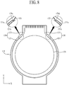
- FIG. 8 is a view illustrating another modified example of a driving power supply line shown in FIG. 1 .
- a circumference line of the driving power supply line is formed in a closed loop type. Therefore, in FIG. 8 , a repeated description of elements corresponding to the same reference numerals as those of FIG. 1 will be omitted, and the driving power supply line will only be described hereinafter.
- the driving power supply line 150 may include a circumference line 151, and first and second shoulder lines 153 and 155.
- the circumference line 151 is formed in a closed loop type along the circumference of the other circular display portion 120 except one side of the circular display portion 120 adjacent to the driving circuit connecting portion 113. It is preferable that the circumference line 151 is formed in a concentric circle with at least one of an outer sidewall of the substrate 110 and the circular display portion 120.
- the circumference line 151 may include a first curve portion 151a, a second curve portion 151b, a first connecting portion 151c, and a second connecting portion 151d.
- the first curve portion 151a is formed along the circumference of the other circular display portion 120 except one side of the circular display portion 120 in parallel with the circular display portion 120. At this time, it is preferable that the first curve portion 151a is formed in a concentric circle with at least one of the outside wall of the substrate 110 and the circular display portion 120.
- the second curve portion 151b is formed to be spaced apart from the first curve portion 151a at a certain distance while being arranged in parallel with the first curve portion 151a.
- the first connecting portion 151c electrically connects one ends of the first and second curve portions 151a and 151b to each other, wherein the one ends of the first and second curve portions 151a and 151b are adj acent to each other. Therefore, the one ends of the first and second curve portions 151a and 151b are connected to each other seamlessly by the first connecting portion 151c.
- the second connecting portion 151d electrically connects the other ends of the first and second curve portions 151a and 151b to each other, wherein the other ends of the first and second curve portions 151a and 151b are adjacent to each other. Therefore, the other ends of the first and second curve portions 151a and 151b are connected to each other seamlessly by the second connecting portion 151d.
- Each of the first curve portion 151a, the second curve portion 151b, the first connecting portion 151c and the second connecting portion 151d may be formed on the same layer on the substrate 110.
- the circumference line 151 is formed in a closed-loop type along the circumference of the circular display portion 120.
- the first shoulder line 153 is the same as the aforementioned first shoulder line except that the first shoulder line 153 is formed between the first connecting portion 151c of the circumference line 151 and the first driving power pad of the driving pad portion 113a at a certain curvature to connect one end of the circumference line 151 to the first driving power pad.
- the second shoulder line 155 is the same as the aforementioned second shoulder line except that the second shoulder line 155 is formed between the second connecting portion 151d of the circumference line 151 and the second driving power pad of the driving pad portion 113a at a certain curvature to connect the other end of the circumference line 151 to the second driving power pad.
- first curve portion 151a and the second curve portion 151b may be formed on different layers on the substrate 110 to overlap with each other without being formed on the same layer on the substrate 110.
- first 151a and second 151b curve portions have a same radius and are parallel to each other along an axis passing perpendicularly through the display area.
- the first curve portion 151a may be formed on the same layer as the data line DL
- the second curve portion 151b may be formed on the same layer as the anode electrode of the organic light emitting diode to overlap the first curve portion 151a.
- the first connecting portion 151c electrically connects the one ends of the first and second curve portions 151a and 151b to each other through a first contact hole (not shown), and the second connecting portion 151d electrically connects the other ends of the first and second curve portions 151a and 151b to each other through a second contact hole (not shown). Therefore, according to the present invention, the driving power supply line 150 having a closed loop type may be formed even though the formation area of the driving power supply line 150 is not increased.
- the pixel driving power source Vdd is supplied to each pixel P by using the driving power supply line 150 including the circumference line 151 of the closed loop type to minimize voltage drop of the pixel driving power source Vdd, whereby picture quality deterioration caused by voltage drop of the pixel driving power source Vdd may be minimized or avoided.
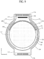
- FIG. 9 is a view illustrating a modified example of a display device according to the present invention, which is shown in FIGS. 1 to 8 .
- a selective portion is additionally provided. Therefore, in FIG. 9 , a repeated description of elements corresponding to the same reference numerals as those of FIG. 1 will be omitted, and the selective portion and its related elements will only be described hereinafter.
- the selective portion 170 includes a plurality of selective circuits 172 formed along the circumference of the circular display portion 120 and connected to two or more data lines DL.
- Each of the plurality of selective circuits 172 is connected to a plurality of data groups, each of which includes two or more data lines, one to one, thereby driving the data lines, which are included in each data group, based on time division.
- Each of the plurality of selective circuits 172 may be a multiplexing circuit, for example, multiplexer, which has one input terminal and two or more output terminals.
- a data signal Vdata is supplied from the driving circuit portion 130 to each input terminal of the plurality of selective circuits 172.
- the output terminals of each of the plurality of selective circuits 172 are connected to the data lines, which are included in each data group, one to one.
- Each of the plurality of selective circuits 172 supplies the data signal Vdata, which is supplied to the input terminal, to the data lines included in each data group, in due order in response to a time-division selective signal.
- each data group may include three data lines to facilitate driving of the unit pixel.
- each of the plurality of selective circuits 172 may have 3i (i is a natural number) output channels (e.g., one for each of red, blue, and green channels), or 4i output channels (e.g., one for each of red, blue, green, and white channels).
- the number of data lines included in each data group and the number of output terminals of the selective circuit 172 correspond to the number of pixels constituting one unit pixel or an integer multiple of the number of pixels constituting one unit pixel.
- the formation area of the data link lines may be reduced to reduce the length between the first and second circumference points CP1 and CP2, whereby the circular arc portion 111 of the substrate 110 may be formed in a concentric circle with the circular display portion 120.
- the bezel width BW of the display device may be more reduced.
- each pixel is connected to the driving power supply line and a reference line.
- the driving power supply line is formed in the same structure as that of the aforementioned driving power supply line.
- the reference line is formed between the cathode power supply line 160 and the circular display portion 120 to have the same structure as that of the aforementioned driving power supply line, whereby the reference line may supply a reference voltage, which is supplied from the display driving portion, to each pixel.
- each pixel is connected to the driving power supply line and a compensation power line.
- the driving power supply line is formed in the same structure as that of the aforementioned driving power supply line.
- the compensation power line is formed between the cathode power supply line 160 and the circular display portion 120 to have the same structure as that of the aforementioned driving power supply line, whereby the compensation power line may supply a compensation voltage, which is supplied from the display driving portion, to each pixel.
- the structure of the driving power supply line and the connection structure between the driving power supply line and the pixel according to the present invention may equally be applied to the power line supplying the power to the pixel.
- the display device according to the present invention has the following advantages.
- the display device may have a thin bezel width while having the circular display portion.
Landscapes
- Engineering & Computer Science (AREA)
- Physics & Mathematics (AREA)
- Computer Hardware Design (AREA)
- General Physics & Mathematics (AREA)
- Theoretical Computer Science (AREA)
- Microelectronics & Electronic Packaging (AREA)
- Electroluminescent Light Sources (AREA)
- Devices For Indicating Variable Information By Combining Individual Elements (AREA)
- Control Of Indicators Other Than Cathode Ray Tubes (AREA)
Claims (12)
- Organische lichtemittierende Diodenanzeigevorrichtung, "OLED", die Folgendes umfasst:ein Substrat (110), umfassend einen kreisförmigen Teil (111) und einen mit dem kreisförmigen Teil (111) verbundenen Ansteuerungsschaltungsverbindungsteil (113), wobei der kreisförmige Teil (111) kreisförmig um einen Mittelpunkt ist;einen Anzeigebereich innerhalb des kreisförmigen Teils (111), wobei der Anzeigebereich eine kreisförmige Form aufweist, die um den Mittelpunkt zentriert ist, wobei der Anzeigebereich mehrere OLED-Pixel umfasst, wobei jedes OLED-Pixel mit einer von mehreren Leistungsleitungen (PL) verbunden ist;einen Ansteuerungsschaltungsteil (130), angeordnet zum Ansteuern der mehreren OLED-Pixel unter Verwendung von Bilddaten, eines Steuersignals und einer Ansteuerungsspannung, wobei die Bilddaten, das Steuersignal und die Ansteuerungsspannung vom Ansteuerungsschaltungsteil über einen Ansteuerungsleistenteil (113a) zugeführt werden, wobei sich der Ansteuerungsleistenteil (113a) im Ansteuerungsschaltungsverbindungsteil (113) befindet;eine Ansteuerungsstromversorgungsleitung (150), ein erstes Ende und ein zweites Ende umfassend, wobei das erste und das zweite Ende jeweils mit einer zugehörigen Ansteuerungsleistungsleiste des Ansteuerungsleistenteils (113a) verbunden sind, wobei die Ansteuerungsstromversorgungsleitung (150) rund um den kreisförmigen Teil gebildet und dazu ausgelegt ist, eine Ansteuerungsspannung für die OLED-Pixel bereitzustellen, wobei die Ansteuerungsstromversorgungsleitung (150) eine kreisförmige Form umfasst, die um den Mittelpunkt zentriert und rund um den Anzeigebereich gebildet ist;mehrere Abtastleitungen (SL) und mehrere Datenleitungen (DL), die die mehreren Abtastleitungen (SL) kreuzen; undmehrere Leistungsteilungsleitungen (PSL), die sich weg von der Ansteuerungsstromversorgungsleitung (150) entlang einer Richtung (X) parallel zu den mehreren Abtastleitungen (SL) erstrecken, wobei jede der Leistungsteilungsleitungen (PSL) mit einer unterschiedlichen Teilmenge der mehreren Leistungsleitungen (PL) verbunden ist,wobei sich die mehreren Datenleitungen entlang einer ersten Richtung (+Y) erstrecken, die vom Ansteuerungsschaltungsteil (130) in Richtung der mehreren Leistungsteilungsleitungen (PSL) ausgerichtet ist, undwobei sich die mehreren Leistungsleitungen (PL) entlang einer zweiten Richtung (-Y) erstrecken, die von den mehreren Leistungsteilungsleitungen (PSL) in Richtung des Ansteuerungsschaltungsteils (130) ausgerichtet ist, wobei die Leistungsleitungen (PL) parallel mit den Datenleitungen (DL) sind, um keine der Datenleitungen (DL) zu schneiden oder zu kreuzen.
- OLED-Anzeigevorrichtung nach Anspruch 1, wobei die Ansteuerungsstromversorgungsleitung (150) eine Gesamtheit des Anzeigebereichs umgibt, ausgenommen die Region des Anzeigebereichs, die zum Ansteuerungsschaltungsverbindungsteil (113) weist.
- OLED-Anzeigevorrichtung nach einem der vorhergehenden Ansprüche, wobei jede der Leistungsteilungsleitungen (PSL) mit zumindest einer der Leistungsleitungen (PL) verbunden ist.
- OLED-Anzeigevorrichtung nach einem der vorhergehenden Ansprüche, wobei jede der Leistungsleitungen (PL) mit nur einer der Leistungsteilungsleitungen (PSL) verbunden ist.
- OLED-Anzeigevorrichtung nach einem der vorhergehenden Ansprüche, ferner umfassend mehreren Scheinpixel (DP), gebildet zwischen den Pixeln (P) des Anzeigebereichs und einer kreisförmigen Begrenzung des Anzeigebereichs.
- OLED-Anzeigevorrichtung nach einem der vorhergehenden Ansprüche, wobei jedes Pixel (P) Folgendes umfasst:eine OLED, umfassend eine Anode und eine Kathode;einen Ansteuerungstransistor (Tdr), umfassend einen Gate-, einen Source- und einen Drain-Anschluss, wobei der Drain-Anschluss mit einer der Leistungsleitungen (PL) verbunden ist, um die Ansteuerungsspannung zu empfangen, undder Source-Anschluss mit der Anode der OLED verbunden ist.
- OLED-Anzeigevorrichtung nach einem der vorhergehenden Ansprüche, umfassend eine Kathodenstromversorgungsleitung (160), gebildet im kreisförmigen Teil zwischen der Ansteuerungsstromversorgungsleitung (150) und dem Anzeigebereich, wobei eine Kathode jedes Pixels elektrisch mit der Kathodenstromversorgungsleitung (160) verbunden ist,
wobei optional die Kathodenstromversorgungsleitung (160) eine kreisförmige Form umfasst, die rund um den Mittelpunkt zentriert ist. - OLED-Anzeigevorrichtung nach einem der vorhergehenden Ansprüche, wobei der kreisförmige Teil der Ansteuerungsstromversorgungsleitung (150) an jedem Ende mit einem entsprechenden Teil (153) der Ansteuerungsstromversorgungsleitung (150) verbunden ist, der sich in den Ansteuerungsschaltungsverbindungsteil (113) erstreckt.
- OLED-Anzeigevorrichtung nach Anspruch 8, wobei die Ansteuerungsstromversorgungsleitung (150) eine Verbindungsleitung (157) umfasst, die die Teile (153) der Ansteuerungsstromversorgungsleitung (150) verbindet und unter einer Ansteuerungsschaltung gebildet wird, die in dem Ansteuerungsschaltungsverbindungsteil (113) gebildet ist, oder,
wobei der Abschnitt (153) der Ansteuerungsstromversorgungsleitung (150) im kreisförmigen Teil zwei konzentrische Leitungen umfasst, die parallel verbunden sind, gebildet in unterschiedlichen Schichten, um einander zu überlappen, sodass die Leitungen den gleichen Radius haben. - OLED-Anzeigevorrichtung nach einem der vorhergehenden Ansprüche, wobei:die Ansteuerungsschaltung elektrisch mit den Datenleitungen (DL) verbunden ist und wobei sich ein Teil jeder Datenleitung (DL) weg vom Ansteuerungsschaltungsverbindungsteil (113) in Richtung seiner verknüpften physisch verbundenen OLED-Pixel erstreckt;eine Ansteuerungsspannungsleiste im Ansteuerungsschaltungsverbindungsteil (113) ausgebildet ist, wobei die Ansteuerungsspannungsleiste physisch mit einer Ansteuerungsstromversorgungsleitung (150) verbunden ist, die sich weg vom Ansteuerungsschaltungsverbindungsteil (113) erstreckt und die OLED-Pixel umgibt; undwobei jede der Leistungsleitungen (PL) elektrisch mit der Ansteuerungsstromversorgungsleitung (150) gekoppelt ist und sich in Richtung des Ansteuerungsschaltungsverbindungsteils (113) und seiner verknüpften physisch verbundenen OLED-Pixel erstreckt.
- OLED-Anzeigevorrichtung nach Anspruch 1, wobei jede der Leistungsteilungsleitungen (PSL) individuell mit mehreren Pixelgruppen (PG) verbunden ist, die zwei oder mehr Pixel P umfassen.
- OLED-Anzeigevorrichtung nach Anspruch 1, wobei ein Abschnitt (151) der Ansteuerungsstromversorgungsleitung (150), der am kreisförmigen Teil ausgebildet ist, Folgendes umfasst:einen ersten Bogenteil (151a), der rund um den kreisförmigen Teil gebildet ist;einen zweiten Bogenteil (151b), der gebildet ist, um vom ersten Bogenteil (151a) mit einem gewissen Abstand beabstandet zu sein, während er parallel mit dem ersten Bogenteil (151a) angeordnet ist;einen ersten Verbindungsteil (151c), der elektrisch eines der Enden des ersten und des zweiten Bogenteils (151a, 151b) miteinander verbindet, wobei die einen Enden des ersten und des zweiten Bogenteils (151a, 151b) aneinander angrenzend sind; undeinen zweiten Verbindungsteil (151d), der elektrisch die anderen Enden des ersten und des zweiten Bogenteils (151a, 151b) miteinander verbindet, wobei die anderen Enden des ersten und des zweiten Bogenteils (151a, 151b) aneinander angrenzend sind,wobei der Abschnitt (151) der Ansteuerungsstromversorgungsleitung (150) in einer geschlossenen Schleife entlang des kreisförmigen Teils ausgebildet ist.
Applications Claiming Priority (1)
| Application Number | Priority Date | Filing Date | Title |
|---|---|---|---|
| KR1020140094296A KR102295874B1 (ko) | 2014-07-24 | 2014-07-24 | 디스플레이 장치 |
Publications (2)
| Publication Number | Publication Date |
|---|---|
| EP2978024A1 EP2978024A1 (de) | 2016-01-27 |
| EP2978024B1 true EP2978024B1 (de) | 2020-06-24 |
Family
ID=53724078
Family Applications (1)
| Application Number | Title | Priority Date | Filing Date |
|---|---|---|---|
| EP15178332.1A Active EP2978024B1 (de) | 2014-07-24 | 2015-07-24 | Organische lichtemittierende diodenanzeigevorrichtung |
Country Status (4)
| Country | Link |
|---|---|
| US (1) | US9349322B2 (de) |
| EP (1) | EP2978024B1 (de) |
| KR (1) | KR102295874B1 (de) |
| CN (3) | CN105304015B (de) |
Families Citing this family (57)
| Publication number | Priority date | Publication date | Assignee | Title |
|---|---|---|---|---|
| KR102239481B1 (ko) * | 2014-12-31 | 2021-04-13 | 엘지디스플레이 주식회사 | 디스플레이 장치 |
| KR102276995B1 (ko) * | 2015-02-12 | 2021-07-21 | 삼성디스플레이 주식회사 | 비사각형 디스플레이 |
| KR102544696B1 (ko) * | 2015-02-16 | 2023-06-16 | 삼성디스플레이 주식회사 | 원형 터치 패널 및 그 제조 방법 |
| US9940866B2 (en) * | 2015-06-01 | 2018-04-10 | Apple Inc. | Electronic device having display with curved edges |
| KR102483379B1 (ko) * | 2015-09-21 | 2023-01-02 | 삼성디스플레이 주식회사 | 표시장치 |
| JP2017134338A (ja) | 2016-01-29 | 2017-08-03 | 株式会社ジャパンディスプレイ | 表示装置 |
| JP6607798B2 (ja) * | 2016-01-29 | 2019-11-20 | 株式会社ジャパンディスプレイ | 表示装置 |
| US10490122B2 (en) | 2016-02-29 | 2019-11-26 | Samsung Display Co., Ltd. | Display device |
| US11482176B2 (en) * | 2016-02-29 | 2022-10-25 | Samsung Display Co., Ltd. | Display device |
| KR102504129B1 (ko) * | 2016-03-31 | 2023-02-28 | 삼성디스플레이 주식회사 | 표시 장치 |
| KR102666831B1 (ko) | 2016-04-15 | 2024-05-21 | 삼성디스플레이 주식회사 | 표시 장치 |
| KR102517167B1 (ko) * | 2016-04-20 | 2023-04-04 | 삼성전자주식회사 | 전자 장치 및 그 제어 방법 |
| KR102666848B1 (ko) * | 2016-05-17 | 2024-05-21 | 삼성디스플레이 주식회사 | 표시 장치 |
| KR102581759B1 (ko) | 2016-05-23 | 2023-09-25 | 삼성디스플레이 주식회사 | 표시 장치 |
| KR102463226B1 (ko) * | 2016-05-31 | 2022-11-07 | 엘지디스플레이 주식회사 | 광 밸브 패널과 이를 이용한 액정표시장치 |
| KR102403234B1 (ko) * | 2016-06-20 | 2022-05-27 | 삼성디스플레이 주식회사 | 표시 장치 |
| KR102605283B1 (ko) | 2016-06-30 | 2023-11-27 | 삼성디스플레이 주식회사 | 표시 장치 |
| CN109416492B (zh) * | 2016-07-12 | 2021-09-10 | 夏普株式会社 | 液晶显示装置 |
| JP6747156B2 (ja) * | 2016-08-05 | 2020-08-26 | 天馬微電子有限公司 | 表示装置 |
| CN106097977B (zh) * | 2016-08-22 | 2019-01-22 | 武汉华星光电技术有限公司 | 一种有机二极管显示驱动电路、显示面板及电子设备 |
| KR102613863B1 (ko) | 2016-09-22 | 2023-12-18 | 삼성디스플레이 주식회사 | 표시 장치 |
| KR102611958B1 (ko) | 2016-09-23 | 2023-12-12 | 삼성디스플레이 주식회사 | 표시 장치 |
| CN108073003B (zh) * | 2016-11-09 | 2020-08-18 | 元太科技工业股份有限公司 | 显示面板、像素阵列衬底与线路阵列结构 |
| KR102619425B1 (ko) * | 2016-11-21 | 2023-12-29 | 엘지디스플레이 주식회사 | 표시장치 |
| KR102559096B1 (ko) | 2016-11-29 | 2023-07-26 | 삼성디스플레이 주식회사 | 표시 장치 |
| KR102715304B1 (ko) | 2016-11-29 | 2024-10-14 | 삼성디스플레이 주식회사 | 표시 장치 |
| KR102643154B1 (ko) | 2016-12-08 | 2024-03-05 | 삼성디스플레이 주식회사 | 표시 장치 |
| KR102793284B1 (ko) * | 2017-02-21 | 2025-04-10 | 삼성디스플레이 주식회사 | 표시 장치 |
| KR102417989B1 (ko) | 2017-05-23 | 2022-07-07 | 삼성디스플레이 주식회사 | 표시 장치 |
| CN107170783B (zh) * | 2017-05-25 | 2020-02-11 | 上海天马有机发光显示技术有限公司 | 显示面板和显示装置 |
| WO2019009185A1 (ja) * | 2017-07-05 | 2019-01-10 | シャープ株式会社 | アクティブマトリックス基板および表示装置 |
| CN107863359B (zh) * | 2017-11-30 | 2020-08-18 | 武汉天马微电子有限公司 | 一种显示面板和显示装置 |
| KR102328177B1 (ko) * | 2017-12-22 | 2021-11-19 | 삼성디스플레이 주식회사 | 표시 장치 |
| CN108335639B (zh) * | 2018-02-14 | 2020-12-25 | 厦门凌阳华芯科技有限公司 | 一种led显示装置 |
| US10896928B2 (en) | 2018-02-14 | 2021-01-19 | Xiamen Xm-Plus Technology Ltd | Light emitting diode display device |
| CN108447390B (zh) * | 2018-02-27 | 2020-07-03 | 上海天马微电子有限公司 | 环形显示模组和显示装置 |
| CN108646477A (zh) * | 2018-03-27 | 2018-10-12 | 上海中航光电子有限公司 | 阵列基板、显示面板和显示装置 |
| JP7120792B2 (ja) * | 2018-04-10 | 2022-08-17 | Tianma Japan株式会社 | 表示装置 |
| KR102749500B1 (ko) | 2018-12-21 | 2025-01-03 | 삼성디스플레이 주식회사 | 디스플레이 장치 |
| CN109742128B (zh) | 2019-01-28 | 2021-01-01 | 昆山国显光电有限公司 | 显示器及其显示面板 |
| JP7239878B2 (ja) * | 2019-04-22 | 2023-03-15 | 凸版印刷株式会社 | 積層体 |
| KR20210013496A (ko) | 2019-07-26 | 2021-02-04 | 삼성디스플레이 주식회사 | 표시 장치 |
| KR20210014265A (ko) | 2019-07-29 | 2021-02-09 | 삼성디스플레이 주식회사 | 디스플레이 장치 |
| KR102930811B1 (ko) * | 2020-04-13 | 2026-02-25 | 삼성디스플레이 주식회사 | 표시 장치 |
| WO2021237725A1 (zh) | 2020-05-29 | 2021-12-02 | 京东方科技集团股份有限公司 | 显示基板和显示装置 |
| US12156443B2 (en) | 2020-08-07 | 2024-11-26 | Beijing Boe Technology Development Co., Ltd. | Display substrate and display device |
| KR102938603B1 (ko) * | 2020-08-24 | 2026-03-12 | 삼성디스플레이 주식회사 | 디스플레이 장치 |
| US11721291B2 (en) | 2020-09-18 | 2023-08-08 | Chengdu Boe Optoelectronics Technology Co., Ltd. | Display substrate and display apparatus |
| KR102775746B1 (ko) * | 2020-11-03 | 2025-03-06 | 구글 엘엘씨 | 라운드형 모서리 베젤 크기를 줄인 디스플레이 디바이스 |
| US11232737B2 (en) | 2021-05-28 | 2022-01-25 | Google Llc | Trace design to reduce bezel area |
| US11665513B2 (en) | 2021-07-13 | 2023-05-30 | International Business Machines Corporation | Multi-device power management |
| CN114122011B (zh) * | 2021-11-10 | 2025-07-22 | 武汉天马微电子有限公司 | 显示面板及显示装置 |
| CN114255671B (zh) * | 2021-12-17 | 2024-10-01 | 重庆惠科金渝光电科技有限公司 | 微型发光二极管显示面板和显示装置 |
| CN114708833B (zh) * | 2022-03-31 | 2023-07-07 | 武汉天马微电子有限公司 | 显示面板及其驱动方法、显示装置 |
| TWI791404B (zh) * | 2022-05-18 | 2023-02-01 | 友達光電股份有限公司 | 顯示面板 |
| KR20240011919A (ko) * | 2022-07-19 | 2024-01-29 | 삼성디스플레이 주식회사 | 표시장치 및 이의 제조방법 |
| CN118355427A (zh) * | 2022-11-15 | 2024-07-16 | 京东方科技集团股份有限公司 | 阵列基板和显示装置 |
Citations (2)
| Publication number | Priority date | Publication date | Assignee | Title |
|---|---|---|---|---|
| EP1557815A2 (de) * | 2004-01-22 | 2005-07-27 | Seiko Epson Corporation | Elektrooptische Vorrichtung und elektronisches Gerät |
| US20060146211A1 (en) * | 2002-06-11 | 2006-07-06 | Koninklijke Philips Electronics N.V. Groenewoudseweg 1 | Non rectangular display device |
Family Cites Families (38)
| Publication number | Priority date | Publication date | Assignee | Title |
|---|---|---|---|---|
| US6525997B1 (en) * | 2000-06-30 | 2003-02-25 | International Business Machines Corporation | Efficient use of display real estate in a wrist watch display |
| US6977868B2 (en) * | 2002-02-14 | 2005-12-20 | Fossil, Inc | Method and apparatus for synchronizing data between a watch and external digital device |
| JP2003316284A (ja) * | 2002-04-24 | 2003-11-07 | Sanyo Electric Co Ltd | 表示装置 |
| JP4574130B2 (ja) | 2003-06-18 | 2010-11-04 | 株式会社半導体エネルギー研究所 | 半導体装置、電子機器 |
| KR100581903B1 (ko) * | 2004-03-09 | 2006-05-22 | 삼성에스디아이 주식회사 | 전계 발광 디스플레이 장치 |
| KR100604053B1 (ko) * | 2004-10-13 | 2006-07-24 | 삼성에스디아이 주식회사 | 발광 표시장치 |
| KR101227134B1 (ko) * | 2005-07-05 | 2013-01-28 | 엘지디스플레이 주식회사 | 유기전계발광 표시장치 |
| KR101149936B1 (ko) * | 2005-04-26 | 2012-05-30 | 엘지디스플레이 주식회사 | 유기전계발광패널 |
| US20060238463A1 (en) | 2005-04-26 | 2006-10-26 | Lg Electronics Inc. | Electro luminescence display device |
| US20090102824A1 (en) * | 2006-03-15 | 2009-04-23 | Sharp Kabushiki Kaisha | Active matrix substrate and display device using the same |
| KR100846591B1 (ko) | 2006-12-01 | 2008-07-16 | 삼성에스디아이 주식회사 | 유기전계발광 표시장치 및 이의 구동방법 |
| KR100846970B1 (ko) | 2007-04-10 | 2008-07-17 | 삼성에스디아이 주식회사 | 유기전계발광 표시장치 및 그의 구동방법 |
| US20080262932A1 (en) * | 2007-04-20 | 2008-10-23 | Andrew Wareham | Resturant and bar consumer display |
| KR100830331B1 (ko) * | 2007-07-23 | 2008-05-16 | 삼성에스디아이 주식회사 | 유기발광 표시 장치 및 그의 제조 방법 |
| US9626900B2 (en) | 2007-10-23 | 2017-04-18 | Japan Display Inc. | Electro-optical device |
| JP4518199B2 (ja) * | 2007-10-23 | 2010-08-04 | エプソンイメージングデバイス株式会社 | 電気光学装置 |
| KR101416904B1 (ko) | 2007-11-07 | 2014-07-09 | 엘지디스플레이 주식회사 | 유기전계발광 표시장치의 화소 구동 장치 |
| KR101451584B1 (ko) | 2008-10-29 | 2014-10-17 | 엘지디스플레이 주식회사 | 유기발광다이오드표시장치 |
| KR101535929B1 (ko) | 2008-12-02 | 2015-07-10 | 삼성디스플레이 주식회사 | 표시기판, 이를 갖는 표시패널 및 이를 갖는 표시장치 |
| JP5532481B2 (ja) * | 2009-05-13 | 2014-06-25 | Nltテクノロジー株式会社 | カラー画像表示方式、カラーフィルタ基板、カラー画素アレイ基板、画像表示装置及び電子機器 |
| KR101065402B1 (ko) * | 2009-08-13 | 2011-09-16 | 삼성모바일디스플레이주식회사 | 유기 발광 표시 장치 |
| KR101034718B1 (ko) * | 2009-10-13 | 2011-05-17 | 삼성모바일디스플레이주식회사 | 유기전계발광 표시장치 |
| WO2011062043A1 (en) * | 2009-11-20 | 2011-05-26 | Semiconductor Energy Laboratory Co., Ltd. | Method for manufacturing semiconductor device |
| KR101388286B1 (ko) | 2009-11-24 | 2014-04-22 | 엘지디스플레이 주식회사 | 유기발광다이오드 표시장치 및 그 구동방법 |
| US20120314546A1 (en) * | 2010-02-17 | 2012-12-13 | Brewer Donald R | Timepiece with twist restricted flexible display |
| KR101073226B1 (ko) | 2010-03-17 | 2011-10-12 | 삼성모바일디스플레이주식회사 | 유기전계발광 표시장치 |
| KR101094292B1 (ko) * | 2010-05-28 | 2011-12-19 | 삼성모바일디스플레이주식회사 | 유기 발광 표시 장치 |
| KR101374477B1 (ko) | 2010-10-22 | 2014-03-14 | 엘지디스플레이 주식회사 | 유기발광다이오드 표시장치 |
| KR101747719B1 (ko) | 2010-10-29 | 2017-06-27 | 엘지디스플레이 주식회사 | 유기발광다이오드 표시장치 및 그 구동방법 |
| KR101763579B1 (ko) | 2010-12-20 | 2017-08-01 | 엘지디스플레이 주식회사 | 발광 표시 장치 및 그의 구동 방법 |
| KR101756665B1 (ko) | 2010-12-29 | 2017-07-11 | 엘지디스플레이 주식회사 | 유기발광다이오드 표시장치 및 그 구동방법 |
| KR20120076215A (ko) | 2010-12-29 | 2012-07-09 | 엘지디스플레이 주식회사 | 유기전계발광표시장치 |
| KR101362002B1 (ko) | 2011-12-12 | 2014-02-11 | 엘지디스플레이 주식회사 | 유기발광 표시장치 |
| KR101350592B1 (ko) | 2011-12-12 | 2014-01-16 | 엘지디스플레이 주식회사 | 유기발광 표시장치 |
| KR101493226B1 (ko) | 2011-12-26 | 2015-02-17 | 엘지디스플레이 주식회사 | 유기 발광 다이오드 표시 장치의 화소 구동 회로의 특성 파라미터 측정 방법 및 장치 |
| KR101916416B1 (ko) * | 2012-07-30 | 2018-11-08 | 삼성전자주식회사 | 플렉서블 디스플레이 장치 및 그 디스플레이 방법 |
| US9477313B2 (en) * | 2012-11-20 | 2016-10-25 | Samsung Electronics Co., Ltd. | User gesture input to wearable electronic device involving outward-facing sensor of device |
| KR20140109100A (ko) * | 2013-03-05 | 2014-09-15 | 삼성디스플레이 주식회사 | 표시 장치 |
-
2014
- 2014-07-24 KR KR1020140094296A patent/KR102295874B1/ko active Active
-
2015
- 2015-07-23 CN CN201510437742.5A patent/CN105304015B/zh active Active
- 2015-07-23 US US14/806,925 patent/US9349322B2/en active Active
- 2015-07-23 CN CN201811032098.3A patent/CN109243364B/zh active Active
- 2015-07-23 CN CN201810321492.2A patent/CN108711395B/zh active Active
- 2015-07-24 EP EP15178332.1A patent/EP2978024B1/de active Active
Patent Citations (2)
| Publication number | Priority date | Publication date | Assignee | Title |
|---|---|---|---|---|
| US20060146211A1 (en) * | 2002-06-11 | 2006-07-06 | Koninklijke Philips Electronics N.V. Groenewoudseweg 1 | Non rectangular display device |
| EP1557815A2 (de) * | 2004-01-22 | 2005-07-27 | Seiko Epson Corporation | Elektrooptische Vorrichtung und elektronisches Gerät |
Also Published As
| Publication number | Publication date |
|---|---|
| EP2978024A1 (de) | 2016-01-27 |
| CN109243364B (zh) | 2021-09-14 |
| CN108711395B (zh) | 2021-08-24 |
| US20160027380A1 (en) | 2016-01-28 |
| CN105304015B (zh) | 2018-10-02 |
| KR20160013359A (ko) | 2016-02-04 |
| CN108711395A (zh) | 2018-10-26 |
| US9349322B2 (en) | 2016-05-24 |
| CN109243364A (zh) | 2019-01-18 |
| KR102295874B1 (ko) | 2021-08-31 |
| CN105304015A (zh) | 2016-02-03 |
Similar Documents
| Publication | Publication Date | Title |
|---|---|---|
| EP2978024B1 (de) | Organische lichtemittierende diodenanzeigevorrichtung | |
| EP2980854B1 (de) | Organische lichtemittierende diodenanzeigevorrichtung | |
| US9449993B2 (en) | Display apparatus | |
| US10159147B2 (en) | Display apparatus | |
| US11776485B2 (en) | Display apparatus including a branched gate driving circuit and multi-screen display apparatus including the same | |
| US10134825B2 (en) | Organic light emitting diode display | |
| CN107845642B (zh) | 显示装置 | |
| KR20140037655A (ko) | 표시 패널 | |
| US11789574B2 (en) | Light emitting display apparatus | |
| KR20220082123A (ko) | 표시 장치 | |
| KR20260037071A (ko) | 표시패널 및 표시장치 | |
| KR20230072180A (ko) | 표시 장치 및 표시 패널 | |
| JP5123510B2 (ja) | 半導体装置 | |
| KR20220096033A (ko) | 표시패널 및 표시장치 | |
| KR101883890B1 (ko) | 디스플레이 장치 | |
| US20250268040A1 (en) | Display device, display panel and vehicle | |
| KR20230082888A (ko) | 디스플레이 장치 및 디스플레이 구동 방법 | |
| KR20230046609A (ko) | 터치 표시 장치 | |
| US20240224654A1 (en) | Display apparatus | |
| KR20240092233A (ko) | 표시 장치 및 표시 패널 |
Legal Events
| Date | Code | Title | Description |
|---|---|---|---|
| PUAI | Public reference made under article 153(3) epc to a published international application that has entered the european phase |
Free format text: ORIGINAL CODE: 0009012 |
|
| 17P | Request for examination filed |
Effective date: 20150724 |
|
| AK | Designated contracting states |
Kind code of ref document: A1 Designated state(s): AL AT BE BG CH CY CZ DE DK EE ES FI FR GB GR HR HU IE IS IT LI LT LU LV MC MK MT NL NO PL PT RO RS SE SI SK SM TR |
|
| AX | Request for extension of the european patent |
Extension state: BA ME |
|
| RBV | Designated contracting states (corrected) |
Designated state(s): AL AT BE BG CH CY CZ DE DK EE ES FI FR GB GR HR HU IE IS IT LI LT LU LV MC MK MT NL NO PL PT RO RS SE SI SK SM TR |
|
| STAA | Information on the status of an ep patent application or granted ep patent |
Free format text: STATUS: EXAMINATION IS IN PROGRESS |
|
| 17Q | First examination report despatched |
Effective date: 20170530 |
|
| REG | Reference to a national code |
Ref country code: DE Ref legal event code: R079 Ref document number: 602015054633 Country of ref document: DE Free format text: PREVIOUS MAIN CLASS: H01L0027320000 Ipc: G09G0003320000 |
|
| RIC1 | Information provided on ipc code assigned before grant |
Ipc: G09G 3/3233 20160101ALI20191211BHEP Ipc: G09G 3/32 20160101AFI20191211BHEP Ipc: H01L 27/32 20060101ALI20191211BHEP |
|
| GRAP | Despatch of communication of intention to grant a patent |
Free format text: ORIGINAL CODE: EPIDOSNIGR1 |
|
| STAA | Information on the status of an ep patent application or granted ep patent |
Free format text: STATUS: GRANT OF PATENT IS INTENDED |
|
| INTG | Intention to grant announced |
Effective date: 20200122 |
|
| GRAS | Grant fee paid |
Free format text: ORIGINAL CODE: EPIDOSNIGR3 |
|
| GRAA | (expected) grant |
Free format text: ORIGINAL CODE: 0009210 |
|
| STAA | Information on the status of an ep patent application or granted ep patent |
Free format text: STATUS: THE PATENT HAS BEEN GRANTED |
|
| AK | Designated contracting states |
Kind code of ref document: B1 Designated state(s): AL AT BE BG CH CY CZ DE DK EE ES FI FR GB GR HR HU IE IS IT LI LT LU LV MC MK MT NL NO PL PT RO RS SE SI SK SM TR |
|
| REG | Reference to a national code |
Ref country code: GB Ref legal event code: FG4D |
|
| REG | Reference to a national code |
Ref country code: CH Ref legal event code: EP |
|
| REG | Reference to a national code |
Ref country code: AT Ref legal event code: REF Ref document number: 1284674 Country of ref document: AT Kind code of ref document: T Effective date: 20200715 |
|
| REG | Reference to a national code |
Ref country code: DE Ref legal event code: R096 Ref document number: 602015054633 Country of ref document: DE |
|
| REG | Reference to a national code |
Ref country code: IE Ref legal event code: FG4D |
|
| PG25 | Lapsed in a contracting state [announced via postgrant information from national office to epo] |
Ref country code: NO Free format text: LAPSE BECAUSE OF FAILURE TO SUBMIT A TRANSLATION OF THE DESCRIPTION OR TO PAY THE FEE WITHIN THE PRESCRIBED TIME-LIMIT Effective date: 20200924 Ref country code: SE Free format text: LAPSE BECAUSE OF FAILURE TO SUBMIT A TRANSLATION OF THE DESCRIPTION OR TO PAY THE FEE WITHIN THE PRESCRIBED TIME-LIMIT Effective date: 20200624 Ref country code: FI Free format text: LAPSE BECAUSE OF FAILURE TO SUBMIT A TRANSLATION OF THE DESCRIPTION OR TO PAY THE FEE WITHIN THE PRESCRIBED TIME-LIMIT Effective date: 20200624 Ref country code: GR Free format text: LAPSE BECAUSE OF FAILURE TO SUBMIT A TRANSLATION OF THE DESCRIPTION OR TO PAY THE FEE WITHIN THE PRESCRIBED TIME-LIMIT Effective date: 20200925 Ref country code: LT Free format text: LAPSE BECAUSE OF FAILURE TO SUBMIT A TRANSLATION OF THE DESCRIPTION OR TO PAY THE FEE WITHIN THE PRESCRIBED TIME-LIMIT Effective date: 20200624 |
|
| REG | Reference to a national code |
Ref country code: LT Ref legal event code: MG4D |
|
| PG25 | Lapsed in a contracting state [announced via postgrant information from national office to epo] |
Ref country code: RS Free format text: LAPSE BECAUSE OF FAILURE TO SUBMIT A TRANSLATION OF THE DESCRIPTION OR TO PAY THE FEE WITHIN THE PRESCRIBED TIME-LIMIT Effective date: 20200624 Ref country code: HR Free format text: LAPSE BECAUSE OF FAILURE TO SUBMIT A TRANSLATION OF THE DESCRIPTION OR TO PAY THE FEE WITHIN THE PRESCRIBED TIME-LIMIT Effective date: 20200624 Ref country code: LV Free format text: LAPSE BECAUSE OF FAILURE TO SUBMIT A TRANSLATION OF THE DESCRIPTION OR TO PAY THE FEE WITHIN THE PRESCRIBED TIME-LIMIT Effective date: 20200624 Ref country code: BG Free format text: LAPSE BECAUSE OF FAILURE TO SUBMIT A TRANSLATION OF THE DESCRIPTION OR TO PAY THE FEE WITHIN THE PRESCRIBED TIME-LIMIT Effective date: 20200924 |
|
| REG | Reference to a national code |
Ref country code: NL Ref legal event code: MP Effective date: 20200624 |
|
| REG | Reference to a national code |
Ref country code: AT Ref legal event code: MK05 Ref document number: 1284674 Country of ref document: AT Kind code of ref document: T Effective date: 20200624 |
|
| PG25 | Lapsed in a contracting state [announced via postgrant information from national office to epo] |
Ref country code: NL Free format text: LAPSE BECAUSE OF FAILURE TO SUBMIT A TRANSLATION OF THE DESCRIPTION OR TO PAY THE FEE WITHIN THE PRESCRIBED TIME-LIMIT Effective date: 20200624 Ref country code: AL Free format text: LAPSE BECAUSE OF FAILURE TO SUBMIT A TRANSLATION OF THE DESCRIPTION OR TO PAY THE FEE WITHIN THE PRESCRIBED TIME-LIMIT Effective date: 20200624 |
|
| PG25 | Lapsed in a contracting state [announced via postgrant information from national office to epo] |
Ref country code: RO Free format text: LAPSE BECAUSE OF FAILURE TO SUBMIT A TRANSLATION OF THE DESCRIPTION OR TO PAY THE FEE WITHIN THE PRESCRIBED TIME-LIMIT Effective date: 20200624 Ref country code: IT Free format text: LAPSE BECAUSE OF FAILURE TO SUBMIT A TRANSLATION OF THE DESCRIPTION OR TO PAY THE FEE WITHIN THE PRESCRIBED TIME-LIMIT Effective date: 20200624 Ref country code: SM Free format text: LAPSE BECAUSE OF FAILURE TO SUBMIT A TRANSLATION OF THE DESCRIPTION OR TO PAY THE FEE WITHIN THE PRESCRIBED TIME-LIMIT Effective date: 20200624 Ref country code: PT Free format text: LAPSE BECAUSE OF FAILURE TO SUBMIT A TRANSLATION OF THE DESCRIPTION OR TO PAY THE FEE WITHIN THE PRESCRIBED TIME-LIMIT Effective date: 20201026 Ref country code: EE Free format text: LAPSE BECAUSE OF FAILURE TO SUBMIT A TRANSLATION OF THE DESCRIPTION OR TO PAY THE FEE WITHIN THE PRESCRIBED TIME-LIMIT Effective date: 20200624 Ref country code: AT Free format text: LAPSE BECAUSE OF FAILURE TO SUBMIT A TRANSLATION OF THE DESCRIPTION OR TO PAY THE FEE WITHIN THE PRESCRIBED TIME-LIMIT Effective date: 20200624 Ref country code: CZ Free format text: LAPSE BECAUSE OF FAILURE TO SUBMIT A TRANSLATION OF THE DESCRIPTION OR TO PAY THE FEE WITHIN THE PRESCRIBED TIME-LIMIT Effective date: 20200624 Ref country code: ES Free format text: LAPSE BECAUSE OF FAILURE TO SUBMIT A TRANSLATION OF THE DESCRIPTION OR TO PAY THE FEE WITHIN THE PRESCRIBED TIME-LIMIT Effective date: 20200624 |
|
| PG25 | Lapsed in a contracting state [announced via postgrant information from national office to epo] |
Ref country code: SK Free format text: LAPSE BECAUSE OF FAILURE TO SUBMIT A TRANSLATION OF THE DESCRIPTION OR TO PAY THE FEE WITHIN THE PRESCRIBED TIME-LIMIT Effective date: 20200624 Ref country code: PL Free format text: LAPSE BECAUSE OF FAILURE TO SUBMIT A TRANSLATION OF THE DESCRIPTION OR TO PAY THE FEE WITHIN THE PRESCRIBED TIME-LIMIT Effective date: 20200624 Ref country code: IS Free format text: LAPSE BECAUSE OF FAILURE TO SUBMIT A TRANSLATION OF THE DESCRIPTION OR TO PAY THE FEE WITHIN THE PRESCRIBED TIME-LIMIT Effective date: 20201024 |
|
| REG | Reference to a national code |
Ref country code: CH Ref legal event code: PL |
|
| REG | Reference to a national code |
Ref country code: DE Ref legal event code: R097 Ref document number: 602015054633 Country of ref document: DE |
|
| PG25 | Lapsed in a contracting state [announced via postgrant information from national office to epo] |
Ref country code: MC Free format text: LAPSE BECAUSE OF FAILURE TO SUBMIT A TRANSLATION OF THE DESCRIPTION OR TO PAY THE FEE WITHIN THE PRESCRIBED TIME-LIMIT Effective date: 20200624 |
|
| REG | Reference to a national code |
Ref country code: BE Ref legal event code: MM Effective date: 20200731 |
|
| PG25 | Lapsed in a contracting state [announced via postgrant information from national office to epo] |
Ref country code: CH Free format text: LAPSE BECAUSE OF NON-PAYMENT OF DUE FEES Effective date: 20200731 Ref country code: DK Free format text: LAPSE BECAUSE OF FAILURE TO SUBMIT A TRANSLATION OF THE DESCRIPTION OR TO PAY THE FEE WITHIN THE PRESCRIBED TIME-LIMIT Effective date: 20200624 Ref country code: LU Free format text: LAPSE BECAUSE OF NON-PAYMENT OF DUE FEES Effective date: 20200724 Ref country code: LI Free format text: LAPSE BECAUSE OF NON-PAYMENT OF DUE FEES Effective date: 20200731 |
|
| PLBE | No opposition filed within time limit |
Free format text: ORIGINAL CODE: 0009261 |
|
| STAA | Information on the status of an ep patent application or granted ep patent |
Free format text: STATUS: NO OPPOSITION FILED WITHIN TIME LIMIT |
|
| PG25 | Lapsed in a contracting state [announced via postgrant information from national office to epo] |
Ref country code: BE Free format text: LAPSE BECAUSE OF NON-PAYMENT OF DUE FEES Effective date: 20200731 |
|
| 26N | No opposition filed |
Effective date: 20210325 |
|
| PG25 | Lapsed in a contracting state [announced via postgrant information from national office to epo] |
Ref country code: IE Free format text: LAPSE BECAUSE OF NON-PAYMENT OF DUE FEES Effective date: 20200724 Ref country code: SI Free format text: LAPSE BECAUSE OF FAILURE TO SUBMIT A TRANSLATION OF THE DESCRIPTION OR TO PAY THE FEE WITHIN THE PRESCRIBED TIME-LIMIT Effective date: 20200624 |
|
| PG25 | Lapsed in a contracting state [announced via postgrant information from national office to epo] |
Ref country code: TR Free format text: LAPSE BECAUSE OF FAILURE TO SUBMIT A TRANSLATION OF THE DESCRIPTION OR TO PAY THE FEE WITHIN THE PRESCRIBED TIME-LIMIT Effective date: 20200624 Ref country code: MT Free format text: LAPSE BECAUSE OF FAILURE TO SUBMIT A TRANSLATION OF THE DESCRIPTION OR TO PAY THE FEE WITHIN THE PRESCRIBED TIME-LIMIT Effective date: 20200624 Ref country code: CY Free format text: LAPSE BECAUSE OF FAILURE TO SUBMIT A TRANSLATION OF THE DESCRIPTION OR TO PAY THE FEE WITHIN THE PRESCRIBED TIME-LIMIT Effective date: 20200624 |
|
| PG25 | Lapsed in a contracting state [announced via postgrant information from national office to epo] |
Ref country code: MK Free format text: LAPSE BECAUSE OF FAILURE TO SUBMIT A TRANSLATION OF THE DESCRIPTION OR TO PAY THE FEE WITHIN THE PRESCRIBED TIME-LIMIT Effective date: 20200624 |
|
| PGFP | Annual fee paid to national office [announced via postgrant information from national office to epo] |
Ref country code: GB Payment date: 20250520 Year of fee payment: 11 |
|
| P01 | Opt-out of the competence of the unified patent court (upc) registered |
Free format text: CASE NUMBER: APP_26978/2025 Effective date: 20250606 |
|
| PGFP | Annual fee paid to national office [announced via postgrant information from national office to epo] |
Ref country code: FR Payment date: 20250521 Year of fee payment: 11 |
|
| PGFP | Annual fee paid to national office [announced via postgrant information from national office to epo] |
Ref country code: DE Payment date: 20250520 Year of fee payment: 11 |