EP2939036B1 - In-tool esd events monitoring method and apparatus - Google Patents
In-tool esd events monitoring method and apparatus Download PDFInfo
- Publication number
- EP2939036B1 EP2939036B1 EP13821627.0A EP13821627A EP2939036B1 EP 2939036 B1 EP2939036 B1 EP 2939036B1 EP 13821627 A EP13821627 A EP 13821627A EP 2939036 B1 EP2939036 B1 EP 2939036B1
- Authority
- EP
- European Patent Office
- Prior art keywords
- antenna
- esd
- detector
- event
- process area
- Prior art date
- Legal status (The legal status is an assumption and is not a legal conclusion. Google has not performed a legal analysis and makes no representation as to the accuracy of the status listed.)
- Active
Links
Images


Classifications
-
- G—PHYSICS
- G01—MEASURING; TESTING
- G01R—MEASURING ELECTRIC VARIABLES; MEASURING MAGNETIC VARIABLES
- G01R31/00—Arrangements for testing electric properties; Arrangements for locating electric faults; Arrangements for electrical testing characterised by what is being tested not provided for elsewhere
- G01R31/001—Measuring interference from external sources to, or emission from, the device under test, e.g. EMC, EMI, EMP or ESD testing
- G01R31/002—Measuring interference from external sources to, or emission from, the device under test, e.g. EMC, EMI, EMP or ESD testing where the device under test is an electronic circuit
-
- G—PHYSICS
- G01—MEASURING; TESTING
- G01R—MEASURING ELECTRIC VARIABLES; MEASURING MAGNETIC VARIABLES
- G01R31/00—Arrangements for testing electric properties; Arrangements for locating electric faults; Arrangements for electrical testing characterised by what is being tested not provided for elsewhere
- G01R31/001—Measuring interference from external sources to, or emission from, the device under test, e.g. EMC, EMI, EMP or ESD testing
-
- G—PHYSICS
- G01—MEASURING; TESTING
- G01R—MEASURING ELECTRIC VARIABLES; MEASURING MAGNETIC VARIABLES
- G01R35/00—Testing or calibrating of apparatus covered by the other groups of this subclass
- G01R35/005—Calibrating; Standards or reference devices, e.g. voltage or resistance standards, "golden" references
Definitions
- Embodiments of the invention relate generally to an apparatus for electrostatic discharges, "ESD”, events monitoring incorporating a charged device model event simulator, "CDMES", unit, comprising at least one antenna, according to the preamble of claim 1 and a method of monitoring electrostatic discharges, "ESD", events by using said apparatus.
- the method and apparatus disclosed herein provide real time ESD events monitoring, in, for example, integrated circuits (ICs) production tools and/or different processes and assist to prevent ESD related filers using one or more method(s) of the charged device model.
- ICs integrated circuits
- CDM events represent electrostatic discharges which happen in manual and automated production systems for electronic ICs.
- the IC may acquire electrical charges by many ways, such as, for example, by contact, friction, and/or induction from a nearby electrical field just to mention a few possible ways.
- ESD event a relatively high discharge current
- the design of IC components usually incorporates special means (or particular components) for protection against ESD effects.
- the semiconductor industry has developed several standard methods for testing IC devices and defined their CDM ESD threshold parameters such as, e.g., withstand voltage and current amplitude.
- the applicable standards also detail the test apparatus requirements for automated IC CDM tests. These methods and devices are useful during IC designing stages, final testing for product certification, and failure analyses of damaged devices.
- a goal in accordance with various embodiments of this invention is to provide a method and apparatus for real time ESD event monitoring and calibration in IC production tools and manufacturing processes.
- FIG 1a illustrates a typical discharge model 100 of charged (IC) device CDM event in a tool or processing chamber.
- the MiniPulse ESD detector 105 (or another type of ESD detector 105) intercepts the electromagnetic waves 140, and the Robot Placement Effector 115 (or another suitable type of robotic arm 115) places a charged device 125 into a test socket 130.
- the test socket 130 is typically placed on a suitable test bed 131, base 131, or another suitable platform 131.
- a discharge occurs and the antenna 135 (coupled to the MiniPulse Detector 105) intercepts the waves 140 of the discharge event.
- the ESD event is a discharge 141 that takes place in a form of a spark between two conductive parts 125 and 130 that both differ in voltage potential.
- the conductive parts 125 and 130 and other semiconductor processing equipment may be in a tool or processing chamber 132 that may have any suitable size such as, for example, approximately 2x2 feet, 4x4 feet, or other dimensions.
- a current problem with conventional technology is in the difficulty in calibrating an ESD detector. This difficulty is due to, for example, the challenge in providing the repeatability of the discharge events themselves. Other difficulties exist due to conditions imposed upon the radiated electrical field waveform by the materials and configuration of the process point itself. Therefore, the current technology is limited in its capabilities and suffers from at least the above constraints and deficiencies. Embodiments of the invention provide systems and methods for overcoming the difficulties in calibrating the ESD detectors.
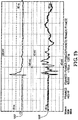
- Figure 1b shows a screen shot of a typical example voltage/current waveform of a CDM electrostatic event where a discharge takes place in a form of a spark between two conductive parts.
- the top waveform 180 is an example output signal (current pulse) that is similar to an example output signal that is produced by a CDMES (Charged Device Model Event Simulator) as will be discussed below in accordance with an embodiment of the invention.
- the lower waveform 185 is an example MicroESD antenna 135 response to an incident propagating field.
- the top waveform 180 shows a pulse signal that is similar to a pulse signal that can also be generated and/or simulated from a CDMES device to be discussed below in accordance with an embodiment of the invention.
- the bottom waveform 185 shows the radiated signal being detected by the antenna 135 coupled to the MiniPulse detector 105.
- the MiniPulse detector 105 includes an electronic circuit that is capable of receiving the signal that is intercepted by the antenna 135. The electronic circuit will classify this signal as an ESD event 110 if the electronic circuit determines that this signal is an ESD event of interest based upon an ESD voltage and pulse duration threshold levels as also discussed below.
- an apparatus for electrostatic discharges, "ESD”, events monitoring incorporating a charged device model event simulator, “CDMES”, unit comprises at least one antenna, said at least one antenna being positioned in a process area and configured to receive radiation during calibration; an ESD detector being coupled to said at least one antenna; said ESD detector being wirelessly coupled, by said at least one antenna, to said CDMES unit; and said ESD detector being calibrated for different discharge energies generated by said CDMES unit.
- a method of monitoring electrostatic discharges, "ESD”, events by using the above indicated apparatus includes: detecting a discharge energy; and calibrating an electrostatic detector for different discharge energies.
- first, second, and the like may be used herein to describe various elements, components, parts, regions, layers, chambers, and/or sections, these elements, components, parts, regions, layers, chambers, and/or sections should not be limited by these terms. These terms are only used to distinguish one element, component, part, region, layer, chamber, or section from another element, component, part, region, layer, chamber, or section. Thus, a first element, component, part, region, layer, chamber, or section discussed below could be termed a second element, component, part, region, layer, chamber, or section without departing from the teachings of the present invention.
- the charged device model events monitoring system (or apparatus), in accordance with an embodiment of the invention, was developed under consideration that, in general, semiconductor tool processing chambers are essentially echoic chambers with relatively high electrical noise level due to surrounding metal enclosure elements.
- each tool has unique characteristics (e.g., EMI landscape) in reflecting internal electromagnetic field radiation caused by electrostatic discharge events.
- CDM events e.g., EMI landscape
- a charged IC device is discharged when it contacts a tool or process element of a different electric potential. This discharge across a dielectric gap (typically air) causes the dipole formed by the differing electrical potentials to collapse or a capacitor formed between charged IC and tool parts to collapse.
- An embodiment of the invention also provides an ESD event monitor, which is also referred herein as a "MiniPulse" or MiniPulse detector or ESD detector.
- the monitor is, for example, a low-cost event monitor for workstations, electronics production tools, processes, and mobile applications.
- the resulting radiated pulse electromagnetic waveform (radiated signal) is detected by, for example, the MiniPulse detector and an antenna that is communicatively coupled to the MiniPulse detector. If the detected field voltage level of this pulse waveform is above the threshold calibrated with the Charged Device Model Event Simulator (CDMES) equipment, then the MiniPulse detector registers a significant CDM event.
- CDMES Charged Device Model Event Simulator
- the CDM events are, for example, characterized by short (typically less than approximately 4 nano-seconds) duration changes in electromagnetic field and generate, in the antenna, an induced voltage (current) rising signal with a high slew rate. Therefore, regarding in tool ESD monitoring, the detection system used should distinguish a CDM signal of interest from general tool noise in an echoic chamber environment.
- calibration methods for ESD detectors are provided.
- a suitable equipment such as, for example, a CDMES device known in the art, may be used to simulate CDM events, and a calibration method is then performed according to an embodiment of the invention.
- in situ monitoring of CDM events is facilitated by simulating a group of spark gap discharges in the real tool at the point where IC devices contact conductive tool elements.
- the collapsing charged capacitor discharge simulates CDM events at a pre-selected voltage threshold value for a given IC device.
- the tool can be said to be calibrated for IC CDM ESD event detection at the specified level.
- CDMES devices that are known or that would be developed in the future may be used to simulate CDM events, and a calibration method according to an embodiment of an invention is performed after simulating a CDM event or different discharge energies.
- the CDMES is configured in several embodiments as a device with an open moving electrode in the discharge gap, or a mercury or RF relay or high voltage RF relay, for example, reed relay.
- the CDM event simulated discharges generate signals that are intercepted and detected in the receiving antenna of the monitoring device (MiniPulse).
- the MiniPulse antenna (MicroESD antenna) is coupled to the MiniPulse (see Figure 3b ) and permits the MiniPulse to receive the waveforms due to an ESD event.
- the MiniPulse can be calibrated in situ by varying the CDMES discharge voltage and/or the position of the MiniPulse antenna with respect to the expected CDM event source.
- the CDMES is charged device simulator that creates a known radiated spark that is similar to a discharge occurrence when a charged device is approaching or contacting a socket.
- This CDMES is used to calibrate the MiniPulse.
- a DC power supply is coupled to the CDMES, and any suitable power supply voltage values (e.g., 100V, 200V, 500V, or other values) are driven into the CDMES.
- the antenna detects the waveform from the CDMES-created discharge, and the MiniPulse captures and processes the waveform detected by the antenna.
- An example of a waveform due to a CDMES-created discharge is observed in the oscilloscope as shown, for example, in Figure 1b , as also further discussed below.
- the ESD threshold voltage level may be set up (or otherwise configured) for the MiniPulse detector.
- the output alarm signal from the MiniPulse will be generated and may be sent to a tool control system if CDM events exceed the threshold level for real IC discharge events in the tool.
- the CDM Event Simulator has been designed to allow ESD monitors (detectors) to be calibrated inside the tools and processes where CDM events occur.
- This simulation device allows the creation of calibrated CDM events of different voltage amplitudes to be produced at the point where production devices are most vulnerable and where ESD monitoring sensors are located. This approach allows the highest level of handling safety for sensitive devices.
- CDM Event Simulator CDM Event Simulator
- the IC devices are usually characterized for failure thresholds in formal test beds and machines designed to simulate discharges on the various device input and output connections. This information is used to assess risk during all phases of device manufacture and system integration.
- a method is provided by using an ESD event monitoring device and failure threshold information in conjunction with the CDM Event Simulator (CDMES).
- CDMES CDM Event Simulator
- the systems and methods discussed herein may be used in a tool or processing chamber and may also be used in an open work bench, any tabletop, a real environment, or any other suitable environment where a calibrated CDM is radiated (is created) and detected for purposes of calibrating an ESD detector.
- CDMES Version 1 Mechanical Gap to generate CDM Event:
- the first version of the CDM Event Simulator uses a mechanical gap control to simulate a collapsing capacitor event to simulate the electrostatic discharge which occurs between a charged IC and either an object (target) at a different electrical potential or a ground reference.
- this embodiment models the Charged Device Model (CDM) discharge type which is characterized by a fast single-peak pulse waveform of transferred current between the device and ground.
- the CDMES power circuit incorporates high resistance (up to, for example, approximately 100 mega Ohms or more) so that the voltage across the gap is high (approximately 25V-3000V range) and applied current is less than 10 micro amperes across this range.
- Electrostatic discharge would occur for an arbitrary charged contact and typical ground contact (see Figures 1a and 1b ). Therefore, when the CDMES is charged with a power supply voltage, the CDMES will simulate an ESD event that generates a pulse waveform that is detectable by and reproduced in an oscilloscope.
- the CDM pulse as reproduced on the oscilloscope is a graph of the current pulse waveform and corresponds to the classical CDM waveform referenced in all standards documents (IEC 61000-4-2, IS010605, JESD22-C101E).
- the produced waveform also corresponds to the input CDM pulse waveform which formal device test machines (see standards reference above for examples) use to evaluate device ESD susceptibility.
- Figure 2 is a general view of a charged device model events simulator 200 with a discharge head 202 that is electrically coupled to an external HVPS (high voltage power supply) 205 and scope 210.
- HVPS high voltage power supply
- Figure 3a is a typical CDMES pulse waveform representing discharge current pulse produced when a CDMES is triggered.
- a voltage discharge of, for example, approximately 100V from the HVPS 205 will trigger the CDMES to produce a typical current pulse 305 in the waveform 310.
- This typical current pulse 305 will cause an electrostatic event where a discharge takes place in a form of a spark between two conductive parts.
- Figure 3b is a diagram of a system 350 (or apparatus 350) including a charged device model event simulator 352 (or CDMES 352 or CDMES unit 352), and wherein the system 350 is configured to also provide a calibration method for an ESD event detector 355, in accordance with an embodiment of the invention. Therefore, Figure 3b illustrates a depiction of CDMES ESD calibration for MiniPulse ESD Event Detector 355.
- the ESD simulation performed by the CDMES 352, and a calibration method for the ESD event detector 355, may be in real tool or processing chamber 362 (in-situ).
- embodiments of the CDMES may instead be used in an open work bench, any tabletop, a real environment, or any other suitable environment where a calibrated CDM is created and detected for purposes of calibrating an ESD detector.
- the CDMES 352 is coupled with (and operate with) the HVPS 205 and the scope 210.
- the CDMES 352 is electrically coupled via the electrical link 266 (e.g., cable) to the power supply 205 for supplying voltage to the CDMES 352.
- the CDMES 352 is also electrically coupled via the electrical link 267 (e.g., cable) to the oscilloscope 210 which detects and measures the output signal (current pulse) (see output signal 310 in Figure 3a ) that is produced by the CDMES device 352 as discussed further below.
- the CDMES 352 uses the voltage from the HVPS 205 and an internal ESD event generating mechanism to produce a current pulse event.
- the discharge head (of CDMES 352) is charged by the voltage from the HVPS 205.
- the antenna 382 (coupled to the ESD detector 355) intercepts the radiation 380 (or electromagnetic waves 380) of the discharge event generated within the CDMES 352.
- the antenna 382 is configured to detect the different discharge energies in the radiation 380.
- the simulation of the ESD event by use of the CDMES 352 and corresponding elements may be performed in the chamber 362 or may be performed outside of the chamber 362 (i.e., may be performed in an open work bench, any tabletop, a real environment, or any other suitable environment where a calibrated CDM is created and detected for purposes of calibrating an ESD detector 355).
- FIG. 3b shows radiation 380 in the direction of the NULL field, as the antenna 382 is along the axis of and perpendicular to the radiating element (discharge head) of CDMES 352. Any signal will be largely due to reflections. If the CDMES 352 were rotated approximate 90 degrees CCW the signal would be significantly affected.
- the CDMES 352 is discharged at the point where normal device handling occurs, simulating a device CDM discharge event.
- the ESD detector 355 (MiniPulse 355) has a relay output to inform a tool control system of ESD events.
- a gate detect input in the ESD detector 355 is a Test Point which may be utilized to setup the ESD trigger threshold level of the MiniPulse 355, where an ESD trigger threshold level will distinguish ESD events of interest.
- the relay output of the ESD detector 355 may be used to monitor the MiniPulse Alarm status (of Minipulse 355).
- the relay output is, for example, an open collector driver which is pulled to ground concurrently with the audible alarm sounding from the MiniPulse 355.
- various supply voltage values e.g., approximately 20V, 100V, 500V, or other values
- the collapsing capacitor of CDMES 352 allows the user to simulate the desired ESD event strength.
- This method of CDM calibration disclosed herein in an embodiment of the invention has a number of possible benefits that may be one or more of the following.
- the four main features of the novel ESD events detector are:
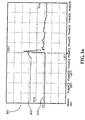
- FIG. 3c is a diagram of a system (or apparatus) 388, in accordance with another embodiment of the invention.
- the system 388 is shown in a top plan view for purposes of clarity of discussion.
- the system 388 is configured for electrostatic discharges (ESD) events monitoring and incorporates a charged device model event simulator (CDMES) unit.
- ESD electrostatic discharges
- CDMES charged device model event simulator
- the system 388 includes at least one antenna 382a that is positioned in a process area 389a, and an ESD detector 355 coupled to the antenna 382a. Since the antenna 382 a is configured to receive the radiation 380 from a CDMES unit 352, the antenna 382a is wirelessly coupled to the CDMES unit 352. The ESD detector 355 is calibrated for different discharge energies generated by the CDMES unit 352.
- the process area 389a may be, for example, a tool process area or an area external to a tool process area.
- a process area (generally shown as area 389) includes a first process area 389a and a second process area 389b.
- the first antenna 382a is positioned in the first process area 382a and a second antenna 382b positioned in the second process area 389b.
- the first antenna 382a is coupled to the ESD detector 355 and the second antenna 382b is also coupled to ESD detector 355.
- the second antenna 382b is coupled to another ESD detector 356 and is not coupled to the ESD detector 355.
- the first process area 389a is separated from the second process area 389b by a distance 391, and the first antenna 382a and second antenna 382b form multi-channels.
- the distance 391 is adjustable.
- the first antenna 382a and second antenna 382b may be similar in an antenna response sensitivity. In another embodiment, the first antenna 382a and second antenna 382b are different in antenna response sensitivities.
- the process areas 389 may vary in number from one or more process areas. Therefore, more than two process areas may be included in the system 388.
- At least one of the process areas 389 may include a socket 373 ( Figure 3b ) that is configured to receive a semiconductor chip 125 ( Figure 1a ), or may include a plurality of sockets 373 that are configured to receive a plurality of semiconductor chips.
- At least one of the process areas 389 may include a tweezer 392 that is configured to receive a wafer 393 in another embodiment as best identified by reference 396.
- the tweezer 392 may be another type of wafer processing tool 392.
- At least one of the process areas 389 may include conductive traces 394 that are accessible by a test probe 395 in an embodiment as best identified by reference 397. Any of the process areas 389 may be of another suitable type of area.
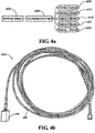
- Antennas used to detect ESD radiated pulse transients have traditionally been standard antennas with very high gain. Whereas this makes detecting ESD events quite easy, it has made it virtually impossible to determine event origins. This weakness has made traditional antennas of little use in monitoring critical processes.
- the "MicroESD” antenna 382 (e.g., the antenna 382 coupled to the MiniPulse detector 355 in Figure 3b ) was developed for the sole purpose of detecting ESD events in close proximity to their source.
- the MicroESD antenna 382 is embodied of various versions of designed microstrip antennas, as shown in the example antennas 405, 410, 415, 420, and/or 425 in Figure 4a , which have excellent ESD near-field radiant pulse reception, while rejecting other near and far-field pulse signatures due to engineered directional gain characteristics. This allows the MicroESD antennas to perform well where other antennas do not in identifying localized ESD events of interest.
- this antenna allows a very wide signal discrimination range (10-3000V) which is not the case with general antennas commonly used in ESD detection due to saturation effects. When used in conjunction with attenuators, very large ESD events can be captured effectively.
- ESD events should preferably be monitored as close to their expected source as practical. Typical monitoring distances for the antenna installation range from, for example, approximately 1" (2.54cm) and approximately 6" (15cm), though other distances can be accommodated.
- the Micro ESD antenna 382 will purposefully become less efficient with greater distance from the source due to signal amplitude reduction and detection threshold settings.
- MiniPulse 355 can be used with multiple concurrent antennas to detect ESD signals in different places simultaneously or separately.
- the same ESD signal sampling method is used, with the only difference being multiple antenna feed points 430.
- the feedpoints 430 are communicatively coupled to the MiniPulse detector 355. Due to the nature of line propagating ESD transients and the low ohmic loss of the antenna cabling, signal degradation is insignificant for the purposes of detection and amplitude discrimination.
- Multiple antennas can be deployed as arrays of dipole structures in almost any configuration.
- Figure 4a five antennas 405-425 are shown.
- the array of dipole structured in Figure 4a may have more than five antennas or less than five antennas.
- FIG 4b is a diagram illustrating a MicroESD antenna assembly 450, in accordance with an embodiment of the invention.
- the assembly 450 includes a MicroESD antenna 455 that is coupled to an electrical link 460 (e.g., a cable 460) which is removably connected to the ESD detector 355 ( Figure 3b ).
- an electrical link 460 e.g., a cable 460
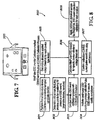
- Figure 5 is a block diagram of an ESD detector 500 (MiniPulse 500), in accordance with an embodiment of the invention.
- Figure 6 is a schematic diagram of the ESD monitor circuit 600 in the ESD detector 600 of Figure 5 , in accordance with an embodiment of the invention.
- the MiniPulse 500 is also shown as (and described as) the ESD detector 355 in Figure 3b .
- the MiniPulse 500 uses a two-dimensional algorithm by analyzing EMI events in the time domain and threshold discrimination to detect pulse electrostatic discharge of certain electromagnetic energy. Through the use of specific antenna configurations and antenna placement relative to the object being monitored, the MiniPulse 500 can provide ESD event detection for specific small areas of interest or for wider area coverage.
- the ESD event signal 501 is detected by an antenna 502 connected to shielded cable and attached to an input connector (e.g., an input SMA connector, Jl).
- the signal 501 is processed by an input filter/integrator 503 (e.g., a 6 order high-pass filter) which is tuned to pass the distorted frequencies (>100MHz) typical of a true ESD event and reject signals outside that range.
- the filtered signal 501 (from the filter/integrator 503) is then passed to a log-amplifier 505 (U2), which is a very fast six stage demodulating log-amp (Analog Devices AD8310).
- the log-amplifier's output signal 506 (U2's output signal 506) is inverted in that the quiescent voltage (no input signal) is approximately 2.5V.
- the circuit filtered incoming signal 506 is discriminated by power, duration, and amplitude.
- the output voltage 506 (U2's output voltage 506) is then compared to a preset DC voltage 507, (TP_Comp 507), using an ultra fast comparator 508 (U3) (Analog Devices AD8561).
- TP_Comp 507 is developed by a separate circuit (the level set block 510 in Figure 5 ) to provide an easily settable alarm level.
- the maximum TP_Comp voltage 507 of ⁇ 2.0 volts is set by the R12 potentiometer and Q4 NPN voltage source which may be checked at TP2.
- the minimum TP_Comp voltage 507 of ⁇ 1.0 volt is set by potentiometer R10 and may be checked at TP1. Potentiometer R13 may then be adjusted through its entire mechanical range to produce TP_Comp 507 between ⁇ 2.0 volts and ⁇ 1.0 volt which matches the output range of the log-amplifier 505.
- U3 the comparator (AD8561) 508, detects a signal (on the "-" or negative input) which goes below TP_Comp 507 (on the "+” or positive input) a negative true condition is momentarily developed on the output of the comparator 508.
- This pulse is then passed to U4a and U4b, a pair of one-shot multi-vibrators.
- An Alarm condition is indicated by, for example, an audible tone, visual red LED and open collector output being triggered "ON".
- the following block diagram and schematic of the MiniPulse 500 shows its basic operating elements.
- the antenna 502 which may be attached directly or remotely via coaxial or triaxial cable, detects EMI signals (e.g., signal 501).
- the antenna 502 is, for example, of the same type as the antenna 382 ( Figure 3b ).
- the EMI signals are processed to detect only those in the frequency range of interest. Since the desired signals have a very large dynamic range a log-amp 505 amplifies to produce a usable signal 506.
- the signal 506 is then passed to a high speed comparator 508 where it is compared with a predetermined threshold voltage level 507.
- Signals that exceed this threshold 507 are then passed to a discriminator 512 which ignores all but those signals that meet the time definition of an EMI pulse of interest.
- This discriminator/generator 512 determines if the EMI pulse is a valid event by checking the slope of the EMI pulse.
- the circuit 512 When triggered, the circuit 512 generates a pulse 514 which is used to indicate an EMI event audibly, visually (e.g., via audio and/or visual indicators 515), and remotely through the open collector output driver transistor 516.
- the alarm output driver 516 sends an output event occurrence signal to a tool or computer, in order to indicate that an event has occurred over the predetermined threshold voltage level.
- Figure 7 shows a general view of a MiniPulse ESD detector 355 as seen externally in one embodiment of the invention.
- the ESD detector 355 may have another type of configuration that differs from Figure 7 .
- FIG 8 is a flowchart of a calibration method 800 and implementation for an ESD detector, in accordance with an embodiment of the invention. It is noted that the order of the steps in the method 800 may vary, and some particular steps may also be performed concurrently.
- formal laboratory device CDM tests are performed on randomly sampled candidate devices.
- a determination is performed on critical manufacturing process points for monitoring for presence of ESD events (examples: testers, handlers).
- in-situ ESD event calibration process is conducted with a CDM Event Simulator (CDMES). Examples of the in-situ ESD event calibration process have been described above with reference to the apparatus 350 in Figure 3b .
- CDMES CDM Event Simulator
- Examples of the in-situ ESD event calibration process have been described above with reference to the apparatus 350 in Figure 3b .
- a continuous ESD monitoring protocol may be instituted with a MiniPulse ESD detector to assure quality compliance.
- this voltage threshold will typically be set at a voltage level that is less than the actual voltage failure level of the device. For example, if a device has an actual voltage failure level of approximately 200 volts, then the voltage threshold will be set below 200 volts such as, e.g., approximately 50% of the voltage failure level or approximately 100 volts. This approach prevents actual damages to occur in devices. Therefore, at 805, an allowable applied voltage threshold is determined for each device type to be tested.
- a minimum statistical sample is applied for PASS/FAIL ESD event detection validation for each location. For example, about 20 or 30 shots, or other number of shots, are applied to obtain accurate calibration.
- an ESD detector 355 (e.g., a MiniPulse detector) is calibrated for specific device withstand voltage threshold. It is noted that after the procedures in blocks 803, 805, and/or 808 are performed, the procedures in block 806 may then be performed.
- the calibration CDMES current pulse waveforms are confirmed by use of an oscilloscope in order to confirm the accuracy of the calibration shots.
- the use of the oscilloscope may also be omitted during this step in the calibration process.
Landscapes
- Physics & Mathematics (AREA)
- General Physics & Mathematics (AREA)
- Electromagnetism (AREA)
- Tests Of Electronic Circuits (AREA)
- Testing Relating To Insulation (AREA)
- Engineering & Computer Science (AREA)
- General Engineering & Computer Science (AREA)
- Elimination Of Static Electricity (AREA)
Applications Claiming Priority (3)
| Application Number | Priority Date | Filing Date | Title |
|---|---|---|---|
| US201261747199P | 2012-12-28 | 2012-12-28 | |
| US14/140,860 US9671448B2 (en) | 2012-12-28 | 2013-12-26 | In-tool ESD events monitoring method and apparatus |
| PCT/US2013/078038 WO2014106075A1 (en) | 2012-12-28 | 2013-12-27 | In-tool esd events monitoring method and apparatus |
Publications (2)
| Publication Number | Publication Date |
|---|---|
| EP2939036A1 EP2939036A1 (en) | 2015-11-04 |
| EP2939036B1 true EP2939036B1 (en) | 2017-05-24 |
Family
ID=51016477
Family Applications (1)
| Application Number | Title | Priority Date | Filing Date |
|---|---|---|---|
| EP13821627.0A Active EP2939036B1 (en) | 2012-12-28 | 2013-12-27 | In-tool esd events monitoring method and apparatus |
Country Status (8)
| Country | Link |
|---|---|
| US (1) | US9671448B2 (enExample) |
| EP (1) | EP2939036B1 (enExample) |
| JP (1) | JP6538566B2 (enExample) |
| KR (1) | KR102054541B1 (enExample) |
| CN (2) | CN105074481A (enExample) |
| SG (1) | SG11201505153VA (enExample) |
| TW (1) | TWI615618B (enExample) |
| WO (1) | WO2014106075A1 (enExample) |
Families Citing this family (29)
| Publication number | Priority date | Publication date | Assignee | Title |
|---|---|---|---|---|
| US11307235B2 (en) | 2012-12-28 | 2022-04-19 | Illinois Tool Works Inc. | In-tool ESD events selective monitoring method and apparatus |
| US10082534B2 (en) * | 2015-06-17 | 2018-09-25 | Intel IP Corporation | Directional pulse injection into a microelectronic system for electrostatic test |
| CN106911742A (zh) * | 2015-12-23 | 2017-06-30 | 深圳长城开发科技股份有限公司 | Esd工业物联网系统 |
| US9804216B2 (en) | 2016-03-16 | 2017-10-31 | International Business Machines Corporation | Detection of electromagnetic field with electroactive polymers |
| US10637234B2 (en) | 2016-06-22 | 2020-04-28 | International Business Machines Corporation | ESD protection circuit |
| TWI752076B (zh) * | 2016-09-16 | 2022-01-11 | 美商伊利諾工具工程公司 | 工具內esd事件的選擇性監控方法及裝置 |
| US9933459B1 (en) * | 2016-11-11 | 2018-04-03 | Fluke Corporation | Magnetically coupled ground reference probe |
| US10782665B2 (en) * | 2017-06-30 | 2020-09-22 | Cattron North America, Inc. | Wireless emergency stop systems, and corresponding methods of operating a wireless emergency stop system for a machine safety interface |
| CN108020698A (zh) * | 2017-12-29 | 2018-05-11 | 江苏林洋能源股份有限公司 | 一种用于电能表防窃电的esd高压检测电路和方法 |
| CN113039443A (zh) * | 2018-09-11 | 2021-06-25 | 迈吉克汽车运动公司 | 用于在电气和/或电子电路上进行测试的工具和组件 |
| EP3918349A1 (en) * | 2018-09-11 | 2021-12-08 | Magicmotorsport Srl | Probe for tools for carrying out tests on electrical and/or electronic circuits and assembly comprising the probe |
| CN109669084A (zh) * | 2018-12-13 | 2019-04-23 | 歌尔科技有限公司 | 设备esd测试方法和系统 |
| WO2020124979A1 (en) * | 2018-12-21 | 2020-06-25 | Huawei Technologies Co., Ltd. | A portable, integrated antenna test bed with built-in turntable |
| CN109686203B (zh) * | 2019-01-29 | 2023-11-21 | 中国人民解放军陆军工程大学 | 静电电磁脉冲诱发空气式静电放电实验系统 |
| US10805936B1 (en) * | 2019-07-24 | 2020-10-13 | Cypress Semiconductor Corporation | Device, system and methods for mitigating interference in a wireless network |
| CN110646695B (zh) * | 2019-09-29 | 2021-07-23 | 潍坊歌尔微电子有限公司 | 一种静电测试工装 |
| DE102019217083A1 (de) * | 2019-11-06 | 2021-05-06 | Robert Bosch Gmbh | Überwachungsanordnung zur Erkennung von Zuleitungsfehlern für ein Steuergerät |
| TWI772713B (zh) | 2019-11-18 | 2022-08-01 | 和碩聯合科技股份有限公司 | 天線裝置及其靜電防護方法 |
| KR102769072B1 (ko) * | 2020-09-22 | 2025-02-18 | 삼성전자주식회사 | Esd 테스트 방법 및 이를 수행하는 esd 테스트 시스템 |
| CN112698114B (zh) * | 2020-12-10 | 2023-04-14 | 北京无线电测量研究所 | 一种天线近场数据采集方法和系统 |
| CN113158441B (zh) * | 2021-03-31 | 2024-12-17 | 胜达克半导体科技(上海)股份有限公司 | 一种芯片测试机内提高抓取信号精度的方法 |
| CN113904736B (zh) * | 2021-09-18 | 2023-05-23 | 中国电子科技集团公司第二十九研究所 | 一种多通道射频信号路由装置 |
| KR20230064052A (ko) | 2021-11-02 | 2023-05-10 | 삼성전자주식회사 | 반도체 장치 |
| TWI792820B (zh) * | 2021-12-30 | 2023-02-11 | 趙文煌 | 1kV以下的電源迴路絕緣劣化偵測預警裝置 |
| TWI806647B (zh) * | 2022-06-08 | 2023-06-21 | 英業達股份有限公司 | 射頻及電磁干擾的自動測試系統及其方法 |
| KR20230169599A (ko) | 2022-06-09 | 2023-12-18 | 삼성전자주식회사 | 전류 검출 회로를 갖는 집적 회로 및 그것의 동작 방법 |
| CN116298648B (zh) * | 2023-05-12 | 2023-09-19 | 合肥联宝信息技术有限公司 | 一种静电路径的检测方法、装置及电子设备 |
| TWI848814B (zh) * | 2023-09-08 | 2024-07-11 | 英業達股份有限公司 | 靜電放電量測裝置 |
| TWI855857B (zh) * | 2023-09-08 | 2024-09-11 | 英業達股份有限公司 | 靜電放電量測方法 |
Family Cites Families (25)
| Publication number | Priority date | Publication date | Assignee | Title |
|---|---|---|---|---|
| US2909190A (en) | 1958-10-29 | 1959-10-20 | Exxon Research Engineering Co | Static electricity detection and control system |
| EP0425823A1 (en) | 1989-09-29 | 1991-05-08 | Antivision Systems Corp. | Electrocstatic imaging apparatus |
| US5359319A (en) | 1990-08-13 | 1994-10-25 | Minnesota Mining And Manufacturing Company | Electrostatic discharge detector and display |
| US5315255A (en) | 1992-07-16 | 1994-05-24 | Micron Technology, Inc. | Non-contact, electrostatic, discharge detector |
| CN1162746A (zh) * | 1996-04-15 | 1997-10-22 | 三菱电机株式会社 | 微波探测器 |
| WO1998000676A1 (en) | 1996-06-28 | 1998-01-08 | Intelligent Enclosures Corporation | Environmentally enhanced enclosure for managing cmp contamination |
| US5903220A (en) * | 1997-04-17 | 1999-05-11 | Lucent Technologies Inc. | Electrostatic discharge event detector |
| US5923160A (en) * | 1997-04-19 | 1999-07-13 | Lucent Technologies, Inc. | Electrostatic discharge event locators |
| AU2001280444A1 (en) | 2000-06-26 | 2002-01-08 | Integral Solutions, International | Cdm simulator for testing electrical devices |
| DE10060284C2 (de) | 2000-12-05 | 2003-07-17 | Bruker Biospin Ag Faellanden | Magnetanordnung mit einem aktiv abgeschirmten supraleitenden Magnetspulensytem und einem zusätzlichen Strompfad zur Streufeldunterdrückung im Quenchfall |
| JP2003028921A (ja) * | 2001-07-18 | 2003-01-29 | Nec Corp | 静電破壊試験方法及び試験装置 |
| KR20040030106A (ko) * | 2001-08-13 | 2004-04-08 | 허니웰 인터내셔널 인코포레이티드 | 전자장치의 웨이퍼 레벨 번인 수행 시스템 |
| US7700379B2 (en) * | 2001-08-13 | 2010-04-20 | Finisar Corporation | Methods of conducting wafer level burn-in of electronic devices |
| US7126356B2 (en) * | 2004-04-30 | 2006-10-24 | Intel Corporation | Radiation detector for electrostatic discharge |
| JP2006317432A (ja) * | 2005-04-12 | 2006-11-24 | Nec Electronics Corp | 荷電板及びcdmシミュレータと試験方法 |
| US7525316B2 (en) * | 2005-09-06 | 2009-04-28 | 3M Innovative Properties Company | Electrostatic discharge event and transient signal detection and measurement device and method |
| US7248055B2 (en) | 2005-12-20 | 2007-07-24 | Dell Products L.P. | Electrostatic discharge transient and frequency spectrum measurement of gap discharge |
| US20070164747A1 (en) * | 2005-12-23 | 2007-07-19 | Intel Corporation | Method and apparatus for simulating electrostatic discharge events in manufacturing and calibrating monitoring equipment |
| US7433165B2 (en) * | 2006-03-17 | 2008-10-07 | Adc Dsl Systems, Inc. | Auto-resetting span-power protection |
| JP2010518412A (ja) * | 2008-02-20 | 2010-05-27 | ヴェリジー(シンガポール) プライベート リミテッド | 静電気放電現象を検出するシステム、方法、及びコンピュータプログラム |
| JP4931252B2 (ja) * | 2008-08-14 | 2012-05-16 | 鹿児島県 | 静電気放電発生箇所の検出方法及び検出装置 |
| US20100117674A1 (en) * | 2008-11-11 | 2010-05-13 | Thermo Fisher Scientific Inc. | Systems and methods for charged device model electrostatic discharge testing |
| US8026736B2 (en) | 2008-12-30 | 2011-09-27 | Intel Corporation | Water-level charged device model for electrostatic discharge test methods, and apparatus using same |
| CN102262202B (zh) * | 2010-05-25 | 2013-05-29 | 上海政申信息科技有限公司 | 静电放电信号处理方法及其处理装置与静电放电检测仪 |
| DK2861999T3 (da) * | 2012-06-14 | 2019-07-08 | Prysmian Spa | Anordning til detektering af partielle udladninger og fremgangsmåde |
-
2013
- 2013-12-26 US US14/140,860 patent/US9671448B2/en active Active
- 2013-12-27 CN CN201380073763.2A patent/CN105074481A/zh active Pending
- 2013-12-27 EP EP13821627.0A patent/EP2939036B1/en active Active
- 2013-12-27 JP JP2015550807A patent/JP6538566B2/ja active Active
- 2013-12-27 CN CN202010947085.XA patent/CN112327069A/zh active Pending
- 2013-12-27 SG SG11201505153VA patent/SG11201505153VA/en unknown
- 2013-12-27 WO PCT/US2013/078038 patent/WO2014106075A1/en not_active Ceased
- 2013-12-27 KR KR1020157019982A patent/KR102054541B1/ko active Active
- 2013-12-30 TW TW102149091A patent/TWI615618B/zh active
Also Published As
| Publication number | Publication date |
|---|---|
| KR20150103088A (ko) | 2015-09-09 |
| TWI615618B (zh) | 2018-02-21 |
| WO2014106075A1 (en) | 2014-07-03 |
| KR102054541B1 (ko) | 2019-12-10 |
| EP2939036A1 (en) | 2015-11-04 |
| US20140184253A1 (en) | 2014-07-03 |
| SG11201505153VA (en) | 2015-08-28 |
| US9671448B2 (en) | 2017-06-06 |
| CN112327069A (zh) | 2021-02-05 |
| JP6538566B2 (ja) | 2019-07-03 |
| TW201432271A (zh) | 2014-08-16 |
| CN105074481A (zh) | 2015-11-18 |
| JP2016502117A (ja) | 2016-01-21 |
Similar Documents
| Publication | Publication Date | Title |
|---|---|---|
| EP2939036B1 (en) | In-tool esd events monitoring method and apparatus | |
| JP7076670B2 (ja) | 偽造及び規格外の電子部品の検出及び特定のための方法及び装置 | |
| US10149169B1 (en) | Non-contact electromagnetic illuminated detection of part anomalies for cyber physical security | |
| EP3513204B1 (en) | In-tool esd events selective monitoring method and apparatus | |
| WO2015027664A1 (zh) | 基于模拟电压信号注入的不同类型局放检测仪主机性能测试方法 | |
| US11307235B2 (en) | In-tool ESD events selective monitoring method and apparatus | |
| CN107192902B (zh) | 一种使用多高斯脉冲的线缆传导敏感度时域测试方法 | |
| US10641820B1 (en) | Automated test equipment with relay hot-switch detection | |
| Ashari et al. | Design and fabrication of vivaldi antenna as partial discharge sensor | |
| Zeitlhoefler et al. | Analysis and Simulation of Antenna Response for Discharge Sensing in Production Environments | |
| US20070139050A1 (en) | Electrostatic discharge transient and frequency spectrum measurement of gap discharge | |
| Zeitlhoefler et al. | ESD risk assessment with Discharge Electrode and Antenna Measurement | |
| Fellner et al. | Quantification of ESD pulses caused by collision of objects | |
| Tamminen et al. | Charged device discharge measurement methods in electronics manufacturing | |
| KR20130132845A (ko) | 전자기기의 변동 전계 내성 검사 장치, 전자기기의 변동 전계 내성 검사 방법 | |
| Oglesbee | Spatial location of electrostatic discharge events within information technology equipment | |
| Wu | Design of Antenna-Driven ESD-Event Detector for Manufacturing Field Control | |
| Tagro et al. | Innovative Magnetic-Field Array Probe for TRUST Integrated Circuits |
Legal Events
| Date | Code | Title | Description |
|---|---|---|---|
| PUAI | Public reference made under article 153(3) epc to a published international application that has entered the european phase |
Free format text: ORIGINAL CODE: 0009012 |
|
| 17P | Request for examination filed |
Effective date: 20150703 |
|
| AK | Designated contracting states |
Kind code of ref document: A1 Designated state(s): AL AT BE BG CH CY CZ DE DK EE ES FI FR GB GR HR HU IE IS IT LI LT LU LV MC MK MT NL NO PL PT RO RS SE SI SK SM TR |
|
| AX | Request for extension of the european patent |
Extension state: BA ME |
|
| DAX | Request for extension of the european patent (deleted) | ||
| 17Q | First examination report despatched |
Effective date: 20160620 |
|
| GRAP | Despatch of communication of intention to grant a patent |
Free format text: ORIGINAL CODE: EPIDOSNIGR1 |
|
| RIC1 | Information provided on ipc code assigned before grant |
Ipc: G01R 35/00 20060101ALI20161216BHEP Ipc: G01R 31/00 20060101AFI20161216BHEP |
|
| INTG | Intention to grant announced |
Effective date: 20170120 |
|
| GRAS | Grant fee paid |
Free format text: ORIGINAL CODE: EPIDOSNIGR3 |
|
| GRAA | (expected) grant |
Free format text: ORIGINAL CODE: 0009210 |
|
| AK | Designated contracting states |
Kind code of ref document: B1 Designated state(s): AL AT BE BG CH CY CZ DE DK EE ES FI FR GB GR HR HU IE IS IT LI LT LU LV MC MK MT NL NO PL PT RO RS SE SI SK SM TR |
|
| REG | Reference to a national code |
Ref country code: GB Ref legal event code: FG4D |
|
| REG | Reference to a national code |
Ref country code: CH Ref legal event code: EP |
|
| REG | Reference to a national code |
Ref country code: IE Ref legal event code: FG4D |
|
| REG | Reference to a national code |
Ref country code: AT Ref legal event code: REF Ref document number: 896278 Country of ref document: AT Kind code of ref document: T Effective date: 20170615 |
|
| REG | Reference to a national code |
Ref country code: DE Ref legal event code: R096 Ref document number: 602013021565 Country of ref document: DE |
|
| REG | Reference to a national code |
Ref country code: NL Ref legal event code: MP Effective date: 20170524 |
|
| REG | Reference to a national code |
Ref country code: LT Ref legal event code: MG4D |
|
| REG | Reference to a national code |
Ref country code: AT Ref legal event code: MK05 Ref document number: 896278 Country of ref document: AT Kind code of ref document: T Effective date: 20170524 |
|
| PG25 | Lapsed in a contracting state [announced via postgrant information from national office to epo] |
Ref country code: FI Free format text: LAPSE BECAUSE OF FAILURE TO SUBMIT A TRANSLATION OF THE DESCRIPTION OR TO PAY THE FEE WITHIN THE PRESCRIBED TIME-LIMIT Effective date: 20170524 Ref country code: GR Free format text: LAPSE BECAUSE OF FAILURE TO SUBMIT A TRANSLATION OF THE DESCRIPTION OR TO PAY THE FEE WITHIN THE PRESCRIBED TIME-LIMIT Effective date: 20170825 Ref country code: HR Free format text: LAPSE BECAUSE OF FAILURE TO SUBMIT A TRANSLATION OF THE DESCRIPTION OR TO PAY THE FEE WITHIN THE PRESCRIBED TIME-LIMIT Effective date: 20170524 Ref country code: LT Free format text: LAPSE BECAUSE OF FAILURE TO SUBMIT A TRANSLATION OF THE DESCRIPTION OR TO PAY THE FEE WITHIN THE PRESCRIBED TIME-LIMIT Effective date: 20170524 Ref country code: AT Free format text: LAPSE BECAUSE OF FAILURE TO SUBMIT A TRANSLATION OF THE DESCRIPTION OR TO PAY THE FEE WITHIN THE PRESCRIBED TIME-LIMIT Effective date: 20170524 Ref country code: NO Free format text: LAPSE BECAUSE OF FAILURE TO SUBMIT A TRANSLATION OF THE DESCRIPTION OR TO PAY THE FEE WITHIN THE PRESCRIBED TIME-LIMIT Effective date: 20170824 Ref country code: ES Free format text: LAPSE BECAUSE OF FAILURE TO SUBMIT A TRANSLATION OF THE DESCRIPTION OR TO PAY THE FEE WITHIN THE PRESCRIBED TIME-LIMIT Effective date: 20170524 |
|
| PG25 | Lapsed in a contracting state [announced via postgrant information from national office to epo] |
Ref country code: NL Free format text: LAPSE BECAUSE OF FAILURE TO SUBMIT A TRANSLATION OF THE DESCRIPTION OR TO PAY THE FEE WITHIN THE PRESCRIBED TIME-LIMIT Effective date: 20170524 Ref country code: LV Free format text: LAPSE BECAUSE OF FAILURE TO SUBMIT A TRANSLATION OF THE DESCRIPTION OR TO PAY THE FEE WITHIN THE PRESCRIBED TIME-LIMIT Effective date: 20170524 Ref country code: IS Free format text: LAPSE BECAUSE OF FAILURE TO SUBMIT A TRANSLATION OF THE DESCRIPTION OR TO PAY THE FEE WITHIN THE PRESCRIBED TIME-LIMIT Effective date: 20170924 Ref country code: BG Free format text: LAPSE BECAUSE OF FAILURE TO SUBMIT A TRANSLATION OF THE DESCRIPTION OR TO PAY THE FEE WITHIN THE PRESCRIBED TIME-LIMIT Effective date: 20170824 Ref country code: RS Free format text: LAPSE BECAUSE OF FAILURE TO SUBMIT A TRANSLATION OF THE DESCRIPTION OR TO PAY THE FEE WITHIN THE PRESCRIBED TIME-LIMIT Effective date: 20170524 Ref country code: SE Free format text: LAPSE BECAUSE OF FAILURE TO SUBMIT A TRANSLATION OF THE DESCRIPTION OR TO PAY THE FEE WITHIN THE PRESCRIBED TIME-LIMIT Effective date: 20170524 |
|
| PG25 | Lapsed in a contracting state [announced via postgrant information from national office to epo] |
Ref country code: CZ Free format text: LAPSE BECAUSE OF FAILURE TO SUBMIT A TRANSLATION OF THE DESCRIPTION OR TO PAY THE FEE WITHIN THE PRESCRIBED TIME-LIMIT Effective date: 20170524 Ref country code: SK Free format text: LAPSE BECAUSE OF FAILURE TO SUBMIT A TRANSLATION OF THE DESCRIPTION OR TO PAY THE FEE WITHIN THE PRESCRIBED TIME-LIMIT Effective date: 20170524 Ref country code: EE Free format text: LAPSE BECAUSE OF FAILURE TO SUBMIT A TRANSLATION OF THE DESCRIPTION OR TO PAY THE FEE WITHIN THE PRESCRIBED TIME-LIMIT Effective date: 20170524 Ref country code: DK Free format text: LAPSE BECAUSE OF FAILURE TO SUBMIT A TRANSLATION OF THE DESCRIPTION OR TO PAY THE FEE WITHIN THE PRESCRIBED TIME-LIMIT Effective date: 20170524 Ref country code: RO Free format text: LAPSE BECAUSE OF FAILURE TO SUBMIT A TRANSLATION OF THE DESCRIPTION OR TO PAY THE FEE WITHIN THE PRESCRIBED TIME-LIMIT Effective date: 20170524 |
|
| REG | Reference to a national code |
Ref country code: DE Ref legal event code: R097 Ref document number: 602013021565 Country of ref document: DE |
|
| PG25 | Lapsed in a contracting state [announced via postgrant information from national office to epo] |
Ref country code: IT Free format text: LAPSE BECAUSE OF FAILURE TO SUBMIT A TRANSLATION OF THE DESCRIPTION OR TO PAY THE FEE WITHIN THE PRESCRIBED TIME-LIMIT Effective date: 20170524 Ref country code: PL Free format text: LAPSE BECAUSE OF FAILURE TO SUBMIT A TRANSLATION OF THE DESCRIPTION OR TO PAY THE FEE WITHIN THE PRESCRIBED TIME-LIMIT Effective date: 20170524 Ref country code: SM Free format text: LAPSE BECAUSE OF FAILURE TO SUBMIT A TRANSLATION OF THE DESCRIPTION OR TO PAY THE FEE WITHIN THE PRESCRIBED TIME-LIMIT Effective date: 20170524 |
|
| PLBE | No opposition filed within time limit |
Free format text: ORIGINAL CODE: 0009261 |
|
| STAA | Information on the status of an ep patent application or granted ep patent |
Free format text: STATUS: NO OPPOSITION FILED WITHIN TIME LIMIT |
|
| 26N | No opposition filed |
Effective date: 20180227 |
|
| PG25 | Lapsed in a contracting state [announced via postgrant information from national office to epo] |
Ref country code: SI Free format text: LAPSE BECAUSE OF FAILURE TO SUBMIT A TRANSLATION OF THE DESCRIPTION OR TO PAY THE FEE WITHIN THE PRESCRIBED TIME-LIMIT Effective date: 20170524 |
|
| REG | Reference to a national code |
Ref country code: CH Ref legal event code: PL |
|
| GBPC | Gb: european patent ceased through non-payment of renewal fee |
Effective date: 20171227 |
|
| REG | Reference to a national code |
Ref country code: IE Ref legal event code: MM4A |
|
| PG25 | Lapsed in a contracting state [announced via postgrant information from national office to epo] |
Ref country code: MT Free format text: LAPSE BECAUSE OF NON-PAYMENT OF DUE FEES Effective date: 20171227 Ref country code: LU Free format text: LAPSE BECAUSE OF NON-PAYMENT OF DUE FEES Effective date: 20171227 |
|
| REG | Reference to a national code |
Ref country code: FR Ref legal event code: ST Effective date: 20180831 |
|
| REG | Reference to a national code |
Ref country code: BE Ref legal event code: MM Effective date: 20171231 |
|
| PG25 | Lapsed in a contracting state [announced via postgrant information from national office to epo] |
Ref country code: FR Free format text: LAPSE BECAUSE OF NON-PAYMENT OF DUE FEES Effective date: 20180102 Ref country code: IE Free format text: LAPSE BECAUSE OF NON-PAYMENT OF DUE FEES Effective date: 20171227 |
|
| PG25 | Lapsed in a contracting state [announced via postgrant information from national office to epo] |
Ref country code: CH Free format text: LAPSE BECAUSE OF NON-PAYMENT OF DUE FEES Effective date: 20171231 Ref country code: LI Free format text: LAPSE BECAUSE OF NON-PAYMENT OF DUE FEES Effective date: 20171231 Ref country code: BE Free format text: LAPSE BECAUSE OF NON-PAYMENT OF DUE FEES Effective date: 20171231 Ref country code: GB Free format text: LAPSE BECAUSE OF NON-PAYMENT OF DUE FEES Effective date: 20171227 |
|
| PG25 | Lapsed in a contracting state [announced via postgrant information from national office to epo] |
Ref country code: MC Free format text: LAPSE BECAUSE OF FAILURE TO SUBMIT A TRANSLATION OF THE DESCRIPTION OR TO PAY THE FEE WITHIN THE PRESCRIBED TIME-LIMIT Effective date: 20170524 Ref country code: HU Free format text: LAPSE BECAUSE OF FAILURE TO SUBMIT A TRANSLATION OF THE DESCRIPTION OR TO PAY THE FEE WITHIN THE PRESCRIBED TIME-LIMIT; INVALID AB INITIO Effective date: 20131227 |
|
| PG25 | Lapsed in a contracting state [announced via postgrant information from national office to epo] |
Ref country code: CY Free format text: LAPSE BECAUSE OF FAILURE TO SUBMIT A TRANSLATION OF THE DESCRIPTION OR TO PAY THE FEE WITHIN THE PRESCRIBED TIME-LIMIT Effective date: 20170524 |
|
| PG25 | Lapsed in a contracting state [announced via postgrant information from national office to epo] |
Ref country code: MK Free format text: LAPSE BECAUSE OF FAILURE TO SUBMIT A TRANSLATION OF THE DESCRIPTION OR TO PAY THE FEE WITHIN THE PRESCRIBED TIME-LIMIT Effective date: 20170524 |
|
| PG25 | Lapsed in a contracting state [announced via postgrant information from national office to epo] |
Ref country code: TR Free format text: LAPSE BECAUSE OF FAILURE TO SUBMIT A TRANSLATION OF THE DESCRIPTION OR TO PAY THE FEE WITHIN THE PRESCRIBED TIME-LIMIT Effective date: 20170524 |
|
| PG25 | Lapsed in a contracting state [announced via postgrant information from national office to epo] |
Ref country code: PT Free format text: LAPSE BECAUSE OF FAILURE TO SUBMIT A TRANSLATION OF THE DESCRIPTION OR TO PAY THE FEE WITHIN THE PRESCRIBED TIME-LIMIT Effective date: 20170524 |
|
| PG25 | Lapsed in a contracting state [announced via postgrant information from national office to epo] |
Ref country code: AL Free format text: LAPSE BECAUSE OF FAILURE TO SUBMIT A TRANSLATION OF THE DESCRIPTION OR TO PAY THE FEE WITHIN THE PRESCRIBED TIME-LIMIT Effective date: 20170524 |
|
| P01 | Opt-out of the competence of the unified patent court (upc) registered |
Effective date: 20230606 |
|
| PGFP | Annual fee paid to national office [announced via postgrant information from national office to epo] |
Ref country code: DE Payment date: 20241227 Year of fee payment: 12 |