EP2930552B1 - Display apparatus and optical apparatus - Google Patents
Display apparatus and optical apparatus Download PDFInfo
- Publication number
- EP2930552B1 EP2930552B1 EP15152708.2A EP15152708A EP2930552B1 EP 2930552 B1 EP2930552 B1 EP 2930552B1 EP 15152708 A EP15152708 A EP 15152708A EP 2930552 B1 EP2930552 B1 EP 2930552B1
- Authority
- EP
- European Patent Office
- Prior art keywords
- light
- light guide
- image forming
- unit
- image
- Prior art date
- Legal status (The legal status is an assumption and is not a legal conclusion. Google has not performed a legal analysis and makes no representation as to the accuracy of the status listed.)
- Active
Links
- 230000003287 optical effect Effects 0.000 title claims description 149
- 238000002834 transmittance Methods 0.000 claims description 86
- 238000003384 imaging method Methods 0.000 claims description 61
- 210000003128 head Anatomy 0.000 claims description 12
- 239000000758 substrate Substances 0.000 description 79
- 238000010586 diagram Methods 0.000 description 78
- 238000005286 illumination Methods 0.000 description 72
- 239000000463 material Substances 0.000 description 59
- 230000004048 modification Effects 0.000 description 38
- 238000012986 modification Methods 0.000 description 38
- 239000004973 liquid crystal related substance Substances 0.000 description 33
- 238000005259 measurement Methods 0.000 description 32
- 239000011159 matrix material Substances 0.000 description 23
- 230000000644 propagated effect Effects 0.000 description 21
- 230000008859 change Effects 0.000 description 18
- 229920003023 plastic Polymers 0.000 description 18
- 239000003086 colorant Substances 0.000 description 16
- 238000003475 lamination Methods 0.000 description 15
- -1 e.g. Substances 0.000 description 14
- 210000001747 pupil Anatomy 0.000 description 14
- 239000004033 plastic Substances 0.000 description 13
- 230000004044 response Effects 0.000 description 12
- 230000000295 complement effect Effects 0.000 description 11
- 238000013461 design Methods 0.000 description 11
- 239000011347 resin Substances 0.000 description 10
- 229920005989 resin Polymers 0.000 description 10
- 239000000853 adhesive Substances 0.000 description 8
- 230000001070 adhesive effect Effects 0.000 description 8
- 238000005401 electroluminescence Methods 0.000 description 8
- 239000011521 glass Substances 0.000 description 8
- 229910052751 metal Inorganic materials 0.000 description 8
- 239000002184 metal Substances 0.000 description 8
- 230000004907 flux Effects 0.000 description 7
- 230000014509 gene expression Effects 0.000 description 6
- 239000004065 semiconductor Substances 0.000 description 6
- XOLBLPGZBRYERU-UHFFFAOYSA-N tin dioxide Chemical compound O=[Sn]=O XOLBLPGZBRYERU-UHFFFAOYSA-N 0.000 description 6
- VYPSYNLAJGMNEJ-UHFFFAOYSA-N Silicium dioxide Chemical compound O=[Si]=O VYPSYNLAJGMNEJ-UHFFFAOYSA-N 0.000 description 5
- 239000000956 alloy Substances 0.000 description 5
- 239000000470 constituent Substances 0.000 description 5
- 230000007613 environmental effect Effects 0.000 description 5
- 239000007788 liquid Substances 0.000 description 5
- 238000005240 physical vapour deposition Methods 0.000 description 5
- GWEVSGVZZGPLCZ-UHFFFAOYSA-N Titan oxide Chemical compound O=[Ti]=O GWEVSGVZZGPLCZ-UHFFFAOYSA-N 0.000 description 4
- 229910045601 alloy Inorganic materials 0.000 description 4
- 230000004397 blinking Effects 0.000 description 4
- 238000005229 chemical vapour deposition Methods 0.000 description 4
- 238000004891 communication Methods 0.000 description 4
- 238000006073 displacement reaction Methods 0.000 description 4
- 239000000203 mixture Substances 0.000 description 4
- 230000033116 oxidation-reduction process Effects 0.000 description 4
- 239000002245 particle Substances 0.000 description 4
- 239000002985 plastic film Substances 0.000 description 4
- BQCADISMDOOEFD-UHFFFAOYSA-N Silver Chemical compound [Ag] BQCADISMDOOEFD-UHFFFAOYSA-N 0.000 description 3
- 239000003795 chemical substances by application Substances 0.000 description 3
- 150000002739 metals Chemical class 0.000 description 3
- 238000000034 method Methods 0.000 description 3
- 238000007639 printing Methods 0.000 description 3
- 238000007789 sealing Methods 0.000 description 3
- 229910052709 silver Inorganic materials 0.000 description 3
- 239000004332 silver Substances 0.000 description 3
- 238000003860 storage Methods 0.000 description 3
- XLOMVQKBTHCTTD-UHFFFAOYSA-N zinc oxide Inorganic materials [Zn]=O XLOMVQKBTHCTTD-UHFFFAOYSA-N 0.000 description 3
- 239000011787 zinc oxide Substances 0.000 description 3
- 229920000178 Acrylic resin Polymers 0.000 description 2
- 239000004925 Acrylic resin Substances 0.000 description 2
- 239000004743 Polypropylene Substances 0.000 description 2
- PPBRXRYQALVLMV-UHFFFAOYSA-N Styrene Chemical compound C=CC1=CC=CC=C1 PPBRXRYQALVLMV-UHFFFAOYSA-N 0.000 description 2
- 230000015556 catabolic process Effects 0.000 description 2
- 229920002678 cellulose Polymers 0.000 description 2
- 238000001723 curing Methods 0.000 description 2
- 238000005520 cutting process Methods 0.000 description 2
- 238000006731 degradation reaction Methods 0.000 description 2
- 230000001419 dependent effect Effects 0.000 description 2
- 239000003989 dielectric material Substances 0.000 description 2
- 238000010494 dissociation reaction Methods 0.000 description 2
- 230000005593 dissociations Effects 0.000 description 2
- 238000004070 electrodeposition Methods 0.000 description 2
- PJXISJQVUVHSOJ-UHFFFAOYSA-N indium(III) oxide Inorganic materials [O-2].[O-2].[O-2].[In+3].[In+3] PJXISJQVUVHSOJ-UHFFFAOYSA-N 0.000 description 2
- AMGQUBHHOARCQH-UHFFFAOYSA-N indium;oxotin Chemical compound [In].[Sn]=O AMGQUBHHOARCQH-UHFFFAOYSA-N 0.000 description 2
- 239000005304 optical glass Substances 0.000 description 2
- 238000000059 patterning Methods 0.000 description 2
- 229920006255 plastic film Polymers 0.000 description 2
- 229920003229 poly(methyl methacrylate) Polymers 0.000 description 2
- 239000004926 polymethyl methacrylate Substances 0.000 description 2
- 229920006324 polyoxymethylene Polymers 0.000 description 2
- 229920001155 polypropylene Polymers 0.000 description 2
- 229920002981 polyvinylidene fluoride Polymers 0.000 description 2
- 229960003351 prussian blue Drugs 0.000 description 2
- 239000013225 prussian blue Substances 0.000 description 2
- 230000009467 reduction Effects 0.000 description 2
- 230000002441 reversible effect Effects 0.000 description 2
- 239000000377 silicon dioxide Substances 0.000 description 2
- 239000005361 soda-lime glass Substances 0.000 description 2
- 238000004544 sputter deposition Methods 0.000 description 2
- 239000000126 substance Substances 0.000 description 2
- 239000012780 transparent material Substances 0.000 description 2
- ZNOKGRXACCSDPY-UHFFFAOYSA-N tungsten trioxide Chemical compound O=[W](=O)=O ZNOKGRXACCSDPY-UHFFFAOYSA-N 0.000 description 2
- 238000001771 vacuum deposition Methods 0.000 description 2
- JMMZCWZIJXAGKW-UHFFFAOYSA-N 2-methylpent-2-ene Chemical compound CCC=C(C)C JMMZCWZIJXAGKW-UHFFFAOYSA-N 0.000 description 1
- ZCYVEMRRCGMTRW-UHFFFAOYSA-N 7553-56-2 Chemical compound [I] ZCYVEMRRCGMTRW-UHFFFAOYSA-N 0.000 description 1
- 239000005294 BK7 Substances 0.000 description 1
- YCKRFDGAMUMZLT-UHFFFAOYSA-N Fluorine atom Chemical compound [F] YCKRFDGAMUMZLT-UHFFFAOYSA-N 0.000 description 1
- 229930040373 Paraformaldehyde Natural products 0.000 description 1
- 229930182556 Polyacetal Natural products 0.000 description 1
- 239000004952 Polyamide Substances 0.000 description 1
- 239000004962 Polyamide-imide Substances 0.000 description 1
- 239000004695 Polyether sulfone Substances 0.000 description 1
- 239000004697 Polyetherimide Substances 0.000 description 1
- 239000004698 Polyethylene Substances 0.000 description 1
- 239000004642 Polyimide Substances 0.000 description 1
- 239000004721 Polyphenylene oxide Substances 0.000 description 1
- 239000004734 Polyphenylene sulfide Substances 0.000 description 1
- 239000004793 Polystyrene Substances 0.000 description 1
- XTXRWKRVRITETP-UHFFFAOYSA-N Vinyl acetate Chemical compound CC(=O)OC=C XTXRWKRVRITETP-UHFFFAOYSA-N 0.000 description 1
- SMEGJBVQLJJKKX-HOTMZDKISA-N [(2R,3S,4S,5R,6R)-5-acetyloxy-3,4,6-trihydroxyoxan-2-yl]methyl acetate Chemical compound CC(=O)OC[C@@H]1[C@H]([C@@H]([C@H]([C@@H](O1)O)OC(=O)C)O)O SMEGJBVQLJJKKX-HOTMZDKISA-N 0.000 description 1
- 238000005299 abrasion Methods 0.000 description 1
- 229940081735 acetylcellulose Drugs 0.000 description 1
- 229920001893 acrylonitrile styrene Polymers 0.000 description 1
- 230000002730 additional effect Effects 0.000 description 1
- 229910052782 aluminium Inorganic materials 0.000 description 1
- XAGFODPZIPBFFR-UHFFFAOYSA-N aluminium Chemical compound [Al] XAGFODPZIPBFFR-UHFFFAOYSA-N 0.000 description 1
- 230000003042 antagnostic effect Effects 0.000 description 1
- 229910052787 antimony Inorganic materials 0.000 description 1
- WATWJIUSRGPENY-UHFFFAOYSA-N antimony atom Chemical compound [Sb] WATWJIUSRGPENY-UHFFFAOYSA-N 0.000 description 1
- 238000003491 array Methods 0.000 description 1
- 230000004888 barrier function Effects 0.000 description 1
- 230000005540 biological transmission Effects 0.000 description 1
- 239000001913 cellulose Substances 0.000 description 1
- 229920002301 cellulose acetate Polymers 0.000 description 1
- 239000011248 coating agent Substances 0.000 description 1
- 238000000576 coating method Methods 0.000 description 1
- 229910052681 coesite Inorganic materials 0.000 description 1
- 229920001940 conductive polymer Polymers 0.000 description 1
- 229920001577 copolymer Polymers 0.000 description 1
- 229910052906 cristobalite Inorganic materials 0.000 description 1
- 210000002858 crystal cell Anatomy 0.000 description 1
- 239000006185 dispersion Substances 0.000 description 1
- 239000002612 dispersion medium Substances 0.000 description 1
- 210000003027 ear inner Anatomy 0.000 description 1
- 230000000694 effects Effects 0.000 description 1
- 230000002708 enhancing effect Effects 0.000 description 1
- 239000003822 epoxy resin Substances 0.000 description 1
- 238000005530 etching Methods 0.000 description 1
- 229910052731 fluorine Inorganic materials 0.000 description 1
- 239000011737 fluorine Substances 0.000 description 1
- 229920002313 fluoropolymer Polymers 0.000 description 1
- 239000011888 foil Substances 0.000 description 1
- HCDGVLDPFQMKDK-UHFFFAOYSA-N hexafluoropropylene Chemical compound FC(F)=C(F)C(F)(F)F HCDGVLDPFQMKDK-UHFFFAOYSA-N 0.000 description 1
- 239000011147 inorganic material Substances 0.000 description 1
- 229910052740 iodine Inorganic materials 0.000 description 1
- 239000011630 iodine Substances 0.000 description 1
- 238000004519 manufacturing process Methods 0.000 description 1
- 239000007769 metal material Substances 0.000 description 1
- 229910044991 metal oxide Inorganic materials 0.000 description 1
- 150000004706 metal oxides Chemical class 0.000 description 1
- 238000013008 moisture curing Methods 0.000 description 1
- 238000012544 monitoring process Methods 0.000 description 1
- 238000005457 optimization Methods 0.000 description 1
- 239000011368 organic material Substances 0.000 description 1
- 239000003960 organic solvent Substances 0.000 description 1
- 229920003207 poly(ethylene-2,6-naphthalate) Polymers 0.000 description 1
- 229920002492 poly(sulfone) Polymers 0.000 description 1
- 229920002647 polyamide Polymers 0.000 description 1
- 229920002312 polyamide-imide Polymers 0.000 description 1
- 229920000767 polyaniline Polymers 0.000 description 1
- 229920001230 polyarylate Polymers 0.000 description 1
- 239000004417 polycarbonate Substances 0.000 description 1
- 229920000515 polycarbonate Polymers 0.000 description 1
- 229920005668 polycarbonate resin Polymers 0.000 description 1
- 239000004431 polycarbonate resin Substances 0.000 description 1
- 229920000647 polyepoxide Polymers 0.000 description 1
- 229920000570 polyether Polymers 0.000 description 1
- 229920006393 polyether sulfone Polymers 0.000 description 1
- 229920001601 polyetherimide Polymers 0.000 description 1
- 229920000573 polyethylene Polymers 0.000 description 1
- 239000011112 polyethylene naphthalate Substances 0.000 description 1
- 229920000139 polyethylene terephthalate Polymers 0.000 description 1
- 239000005020 polyethylene terephthalate Substances 0.000 description 1
- 229920001721 polyimide Polymers 0.000 description 1
- 229920000642 polymer Polymers 0.000 description 1
- 239000002952 polymeric resin Substances 0.000 description 1
- 229920000098 polyolefin Polymers 0.000 description 1
- 229920000069 polyphenylene sulfide Polymers 0.000 description 1
- 229920000128 polypyrrole Polymers 0.000 description 1
- 229920002223 polystyrene Polymers 0.000 description 1
- 229920001343 polytetrafluoroethylene Polymers 0.000 description 1
- 239000004810 polytetrafluoroethylene Substances 0.000 description 1
- 229920000123 polythiophene Polymers 0.000 description 1
- 238000012545 processing Methods 0.000 description 1
- SCUZVMOVTVSBLE-UHFFFAOYSA-N prop-2-enenitrile;styrene Chemical compound C=CC#N.C=CC1=CC=CC=C1 SCUZVMOVTVSBLE-UHFFFAOYSA-N 0.000 description 1
- 230000001012 protector Effects 0.000 description 1
- 238000007493 shaping process Methods 0.000 description 1
- 229910052710 silicon Inorganic materials 0.000 description 1
- 239000010703 silicon Substances 0.000 description 1
- 235000012239 silicon dioxide Nutrition 0.000 description 1
- 229920002050 silicone resin Polymers 0.000 description 1
- 239000011029 spinel Substances 0.000 description 1
- 229910052596 spinel Inorganic materials 0.000 description 1
- 229910052682 stishovite Inorganic materials 0.000 description 1
- 230000002195 synergetic effect Effects 0.000 description 1
- 229920003002 synthetic resin Polymers 0.000 description 1
- 238000012360 testing method Methods 0.000 description 1
- 229920002803 thermoplastic polyurethane Polymers 0.000 description 1
- 229920001187 thermosetting polymer Polymers 0.000 description 1
- 210000002262 tip cell Anatomy 0.000 description 1
- 239000004408 titanium dioxide Substances 0.000 description 1
- 229910052905 tridymite Inorganic materials 0.000 description 1
- 238000007740 vapor deposition Methods 0.000 description 1
- 230000000007 visual effect Effects 0.000 description 1
- YVTHLONGBIQYBO-UHFFFAOYSA-N zinc indium(3+) oxygen(2-) Chemical compound [O--].[Zn++].[In+3] YVTHLONGBIQYBO-UHFFFAOYSA-N 0.000 description 1
Images


Classifications
-
- G—PHYSICS
- G02—OPTICS
- G02B—OPTICAL ELEMENTS, SYSTEMS OR APPARATUS
- G02B27/00—Optical systems or apparatus not provided for by any of the groups G02B1/00 - G02B26/00, G02B30/00
- G02B27/01—Head-up displays
- G02B27/0101—Head-up displays characterised by optical features
-
- G—PHYSICS
- G02—OPTICS
- G02B—OPTICAL ELEMENTS, SYSTEMS OR APPARATUS
- G02B27/00—Optical systems or apparatus not provided for by any of the groups G02B1/00 - G02B26/00, G02B30/00
- G02B27/01—Head-up displays
- G02B27/017—Head mounted
- G02B27/0172—Head mounted characterised by optical features
-
- G—PHYSICS
- G02—OPTICS
- G02B—OPTICAL ELEMENTS, SYSTEMS OR APPARATUS
- G02B23/00—Telescopes, e.g. binoculars; Periscopes; Instruments for viewing the inside of hollow bodies; Viewfinders; Optical aiming or sighting devices
- G02B23/14—Viewfinders
-
- G—PHYSICS
- G02—OPTICS
- G02B—OPTICAL ELEMENTS, SYSTEMS OR APPARATUS
- G02B27/00—Optical systems or apparatus not provided for by any of the groups G02B1/00 - G02B26/00, G02B30/00
- G02B27/01—Head-up displays
- G02B27/017—Head mounted
-
- G—PHYSICS
- G02—OPTICS
- G02B—OPTICAL ELEMENTS, SYSTEMS OR APPARATUS
- G02B5/00—Optical elements other than lenses
- G02B5/32—Holograms used as optical elements
-
- G—PHYSICS
- G02—OPTICS
- G02B—OPTICAL ELEMENTS, SYSTEMS OR APPARATUS
- G02B6/00—Light guides; Structural details of arrangements comprising light guides and other optical elements, e.g. couplings
- G02B6/0001—Light guides; Structural details of arrangements comprising light guides and other optical elements, e.g. couplings specially adapted for lighting devices or systems
- G02B6/0011—Light guides; Structural details of arrangements comprising light guides and other optical elements, e.g. couplings specially adapted for lighting devices or systems the light guides being planar or of plate-like form
-
- G—PHYSICS
- G09—EDUCATION; CRYPTOGRAPHY; DISPLAY; ADVERTISING; SEALS
- G09G—ARRANGEMENTS OR CIRCUITS FOR CONTROL OF INDICATING DEVICES USING STATIC MEANS TO PRESENT VARIABLE INFORMATION
- G09G5/00—Control arrangements or circuits for visual indicators common to cathode-ray tube indicators and other visual indicators
- G09G5/10—Intensity circuits
-
- G—PHYSICS
- G02—OPTICS
- G02B—OPTICAL ELEMENTS, SYSTEMS OR APPARATUS
- G02B27/00—Optical systems or apparatus not provided for by any of the groups G02B1/00 - G02B26/00, G02B30/00
- G02B27/01—Head-up displays
- G02B27/0101—Head-up displays characterised by optical features
- G02B2027/0118—Head-up displays characterised by optical features comprising devices for improving the contrast of the display / brillance control visibility
-
- G—PHYSICS
- G02—OPTICS
- G02B—OPTICAL ELEMENTS, SYSTEMS OR APPARATUS
- G02B27/00—Optical systems or apparatus not provided for by any of the groups G02B1/00 - G02B26/00, G02B30/00
- G02B27/01—Head-up displays
- G02B27/0101—Head-up displays characterised by optical features
- G02B2027/0132—Head-up displays characterised by optical features comprising binocular systems
-
- G—PHYSICS
- G02—OPTICS
- G02B—OPTICAL ELEMENTS, SYSTEMS OR APPARATUS
- G02B27/00—Optical systems or apparatus not provided for by any of the groups G02B1/00 - G02B26/00, G02B30/00
- G02B27/01—Head-up displays
- G02B27/017—Head mounted
- G02B2027/0178—Eyeglass type
-
- G—PHYSICS
- G02—OPTICS
- G02B—OPTICAL ELEMENTS, SYSTEMS OR APPARATUS
- G02B27/00—Optical systems or apparatus not provided for by any of the groups G02B1/00 - G02B26/00, G02B30/00
- G02B27/10—Beam splitting or combining systems
- G02B27/14—Beam splitting or combining systems operating by reflection only
- G02B27/144—Beam splitting or combining systems operating by reflection only using partially transparent surfaces without spectral selectivity
-
- G—PHYSICS
- G09—EDUCATION; CRYPTOGRAPHY; DISPLAY; ADVERTISING; SEALS
- G09G—ARRANGEMENTS OR CIRCUITS FOR CONTROL OF INDICATING DEVICES USING STATIC MEANS TO PRESENT VARIABLE INFORMATION
- G09G2320/00—Control of display operating conditions
- G09G2320/06—Adjustment of display parameters
- G09G2320/0626—Adjustment of display parameters for control of overall brightness
-
- G—PHYSICS
- G09—EDUCATION; CRYPTOGRAPHY; DISPLAY; ADVERTISING; SEALS
- G09G—ARRANGEMENTS OR CIRCUITS FOR CONTROL OF INDICATING DEVICES USING STATIC MEANS TO PRESENT VARIABLE INFORMATION
- G09G2360/00—Aspects of the architecture of display systems
- G09G2360/14—Detecting light within display terminals, e.g. using a single or a plurality of photosensors
- G09G2360/144—Detecting light within display terminals, e.g. using a single or a plurality of photosensors the light being ambient light
Definitions
- the present disclosure relates to a display apparatus and optical apparatus.
- a display apparatus used as a head mounted display is publicly known based on Japanese Patent Application Laid-open No. 2006-209144 , for example.
- This display apparatus in the form of eyeglasses includes, on temples thereof, a reception unit configured to receive an image singal transmitted from an image information transmission source, a drive unit configured to decode the image singal received in the reception unit, a display unit configured to display an image obtained by decoding in the drive unit, and a power supply unit configured to supply power to the reception unit, the drive unit, and the display unit.
- the display unit includes a display including an image output device, an optical member, and a Lippman-Bragg volume hologram sheet.
- an imaging device which images the outside using a compact imaging device attached to eyeglasses.
- an area where an image is displayed on the display apparatus described above is set beyond the viewing field of an observer. So, depending on the environment where the display apparatus is provided, it may be difficult for the observer to immediately recognize that an image is displayed or to immediately recognize that an image is to be displayed. Further, it may be difficult for the observer to easily, reliably, and immediately recognize which part of the outside is imaged by the compact imaging device attached to the eyeglasses.
- a display apparatus having a configuration or a structure that allows an observer to immediately recognize that an image is displayed or allows the observer to recognize that an image is to be displayed.
- an optical apparatus having a configuration or a structure that allows the observer to easily, reliably, and immediately recognize which part of the outside is imaged by an imaging device attached to eyeglasses or the like.
- a display apparatus including: a frame mounted onto a head of an observer; an image display device attached to the frame; and a dimming device configured to adjust the amount of outside light that comes from the outside, light transmittance of a partial area of the dimming device being changed based on a signal for displaying an image on the image display device.
- an optical apparatus including: a frame mounted onto a head of an observer; an imaging device attached to the frame; and a dimming device attached to the frame and configured to adjust the amount of outside light that comes from the outside, a spatial area imaged by the imaging device being displayed on the dimming device.
- an optical apparatus including: a frame mounted onto a head of an observer; a receiving device; and a dimming device attached to the frame and configured to adjust the amount of outside light that comes from the outside, light transmittance of the dimming device being changed based on a signal received by the receiving device.
- the display apparatus according to the embodiment of the present disclosure and the optical apparatuses according to the first and second embodiments of the present disclosure each include the dimming device configured to adjust the amount of outside light that comes from the outside, so that the amount of outside light that comes from the outside can be adequately controlled (can be reduced, for example) by the dimming device. So, for example, in the display apparatus according to the embodiment of present disclosure, an image may be recognized well in the image display device without being disturbed by outside light. In the display apparatus according to the embodiment of the present disclosure, the light transmittance of the partial area of the dimming device is changed based on a signal for displaying an image on the image display device. This allows an observer to easily, reliably, and immediately recognize that an image is displayed.
- this allows the observer to easily and reliably recognize that an image is to be displayed.
- a spatial area imaged by the imaging device is displayed on the dimming device. This allows the observer to easily, reliably, and immediately recognize which part of the outside is imaged by the imaging device.
- light transmittance of the dimming device is changed based on a signal received by the receiving device. This allows the observer to easily, reliably, and immediately recognize that the receiving device receives a signal.
- an image display device may include
- the light guide unit may be transmissive or semi-transmissive (see-through). Specifically, a portion of the light guide unit, which is opposed to at least the pupil of an observer, can be made transmissive or semi-transmissive (see-through), and a landscape can be viewed through the part of the light guide unit.
- the display apparatus according to the embodiment of the present disclosure may include one image display device (monocular type) or two image display devices (binocular type). In the binocular type, based on a signal for displaying an image, light transmittance of a partial area of a dimming device may be changed in the both of the image display devices, or light transmittance of a partial area of the dimming device may be changed in one of the image display devices.
- the term "semi-transmissive" is used in some cases. This term is used in not a meaning that 1/2 (50%) of incident light is transmitted or reflected, but a meaning that part of incident light is transmitted and the rest is reflected.
- the signal for displaying an image on the image display device may be received from the outside.
- information or data on an image displayed on the image display device may be recorded, stored, and saved in a so-called cloud computer or server, for example.
- the display apparatus includes a communication unit, for example, a mobile telephone or a smartphone, or when the display apparatus is combined with the communication unit, various types of information or data may be transmitted and received or exchanged between the cloud computer or server and the display apparatus.
- a signal based on various types of information or data that is, a signal for displaying an image on the image display device may be received.
- a signal for displaying an image on the image display device may be stored in the image display device. It should be noted that an image displayed on the image display device includes various types of information or data.
- the display apparatus including the various desirable forms described above may further include a sensor configured to measure the brightness in the outside environment, and light transmittance of a partial area of the dimming device may be changed based on a measurement result of the brightness in the outside environment obtained by the sensor.
- the sensor may be formed of a well-known illumination sensor, and the control of the sensor may be performed based on a well-known control circuit provided to the image display device.
- Each of the optical apparatuses according to the first and second embodiments of the present disclosure may also include a sensor configured to measure the brightness in the outside environment, and light transmittance of a partial area of the dimming device may be changed based on a measurement result of the brightness in the outside environment obtained by the sensor.
- the dimming device may be attached to the image display device or to a frame.
- the dimming device may be attached to the light guide plate. More specifically, for example, the dimming device may be disposed on a different surface (opposed surface) of the side (surface) on which the image forming unit of the light guide unit is disposed.
- the outer edge of a spatial area imaged by an imaging device may be displayed in the form of a frame in the dimming device.
- light transmittance of an area of the dimming device that corresponds to the spatial area imaged by the imaging device may be made lower than light transmittance of an area of the dimming device that corresponds to the outside of the spatial area imaged by the imaging device.
- the observer sees the spatial area imaged by the imaging device as an area darker than the outside of the spatial area imaged by the imaging device.
- the light transmittance of the area of the dimming device, the area corresponding to the spatial area imaged by the imaging device may be made higher than the light transmittance of an area of the dimming device, the area corresponding to the outside of the spatial area imaged by the imaging device.
- the observer sees the spatial area imaged by the imaging device as an area brighter than the outside of the spatial area imaged by the imaging device.
- the optical apparatus according to the first embodiment of the present disclosure including various desirable forms described above may further include a dimming-device-controlling device, and a position of an area of the dimming device that corresponds to the spatial area imaged by the imaging device may be corrected by the dimming-device-controlling device.
- the optical apparatus according to the first embodiment of the present disclosure includes a mobile phone or a smartphone, for example, or when the optical apparatus is combined with a mobile phone, a smartphone, or a personal computer, the spatial area imaged by the imaging device may be displayed on the mobile phone, the smartphone, or the personal computer.
- the area of the dimming device that corresponds to the spatial area imaged by the imaging device is moved/turned or enlarged/contracted using the dimming-device-controlling device, which can be substituted by the mobile phone, the smartphone, or the personal computer.
- the difference between the spatial area displayed on the mobile phone, the smartphone, or the personal computer and the area of the dimming device that corresponds to the spatial area imaged by the imaging device may be eliminated.
- the display apparatus according to the embodiment of the present disclosure and the optical apparatus according to the first embodiment of the present disclosure including the various desirable forms described above may be combined with each other.
- the display apparatus according to the embodiment of the present disclosure and the optical apparatus according to the second embodiment of the present disclosure including the various desirable forms described above may be combined with each other.
- the optical apparatus according to the first embodiment of the present disclosure and the optical apparatus according to the second embodiment of the present disclosure including the various desirable forms described above may be combined with each other.
- the display apparatus according to the embodiment of the present disclosure, the optical apparatus according to the first embodiment of the present disclosure, and the optical apparatus according to the second embodiment of the present disclosure including the various desirable forms described above may be combined with one another.
- a dimming device may include
- the dimming device of the optical apparatus may include a first substrate, a second substrate opposed to the first substrate, a first electrode and a second electrode provided to the first substrate and the second substrate, respectively, and a light-transmission control material layer sealed between the first substrate and the second substrate. At least one of the first substrate and the second substrate may be attached to a frame, for example.
- the light-transmission control material layer may be an optical shutter formed of a liquid crystal material layer, or may be an optical shutter formed of an inorganic EL (electroluminescence) material layer.
- the optical shutter for use in the dimming device may also be an optical shutter configured by an electrophoretic dispersion liquid including a large number of electrically-charged electrophoretic particles and a dispersion medium colored differently from the electrophoretic particles, an optical shutter configured by application of electrodeposition/dissociation that occurs in response to the reversible oxidation reduction of metal, e.g., silver particles, an optical shutter configured by utilizing color change of substance that occurs in response to the oxidation reduction of an electrochromic material, or an optical shutter configured by controlling the light transmittance by electrowetting.
- the material for the light-transmission control material layer may be TN (Twisted Nematic) liquid crystal, or STN (Super Twisted Nematic) liquid crystal, for example, but this is not restrictive.
- the dimming device includes the light-transmission control material layer that is an optical shutter formed of an inorganic EL material layer, the material for the light-transmission control material layer may be tungsten oxide (WO 3 ), for example, but this is not restrictive.
- the light guide unit and the dimming device are disposed in this order from the observer's side, but this order may be reversed.
- the material of the first and second substrates is specifically exemplified by a transparent glass substrate including soda lime glass and super white glass, a plastic substrate, a plastic sheet, and a plastic film.
- the plastic material is exemplified by polyethylene terephthalate, polyethylene naphthalate, polycarbonate, cellulose ester such as acetylcellulose, fluorinated polymer such as copolymer of polyvinylidene difluoride or polytetrafluoroethylene and hexafluoropropene, polyether such as polyoxymethylene, polyacetal, polystyrene, polyethylene, polypropylene, polyolefin such as methylpentene polymer, polyimide including polyamideimide or polyetherimide, polyamide, polyethersulfone, polyphenylene sulfide, polyvinylidene difluoride, tetraacetyl cellulose, bromphenoxy, polyarylate, polysulfone, and the like.
- the first and second substrates are provided with first and second electrodes, respectively, e.g., so-called transparent electrodes.
- the first and second electrodes are each made of indium tin oxide (ITO, including Sn-doped In 2 O 3 , crystalline ITO, and amorphous ITO), fluorine doped SnO 2 (FTO), IFO (F-doped In 2 O 3 ), antimony doped SnO 2 (ATO), SnO 2 , ZnO (including Al-doped ZnO and B-doped ZnO), indium zinc oxide (IZO), spinel oxide, oxide with YbFe 2 O 4 structure, or conductive polymers including polyaniline, polypyrrole, and polythiophene, for example, but these are not restrictive, or a combination of two or more of them is also possible.
- ITO indium tin oxide
- FTO fluorine doped SnO 2
- IFO F-doped In 2 O 3
- the first and second electrodes may be each formed by physical vapor deposition (PVD) such as vacuum deposition and sputtering, various types of chemical vapor deposition (CVD), or various types of coating, for example. Patterning of the electrodes may be arbitrarily performed by etching, lifting off, or using various types of masks.
- PVD physical vapor deposition
- CVD chemical vapor deposition
- Patterning of the electrodes may be arbitrarily performed by etching, lifting off, or using various types of masks.
- the first and second substrates are bonded together by being sealed at outer edge portions using a sealing agent.
- the sealing agent for use may be various types of resin including thermosetting resin, light curing resin, moisture curing resin, and anaerobic curing resin, e.g., epoxy resin, urethane resin, acrylic resin, vinyl acetate resin, enethiol resin, silicone resin, and modified polymer resin.
- light passing through the dimming device may be colored thereby in a desired color.
- the color selected by the dimming device may be variable or fixed.
- the dimming device may be a laminate of a dimming device colored in red, a dimming device colored in green, and a dimming device colored in blue.
- a color to be selected by the dimming device is not restrictive but may be brown, for example.
- the dimming device may be detachably disposed.
- the dimming device may be attached to the frame by using a screw made of transparent plastic, by forming a groove to the frame for engagement of the dimming device, or by providing a magnet to the frame.
- the frame may be also provided with a slide section to slide the dimming device thereinto.
- the dimming device may be provided with a connector for electrical connection to a control circuit via this connector and a wire. This control circuit is for controlling the light transmittance of the dimming device, and is provided in the control device for controlling the image forming unit, for example.
- the dimming device may be bent.
- a light shielding member may be provided to an area of the light guide unit where light output from the image forming unit is input. This light shielding member is for shielding the light guide unit from outside light.
- Such a configuration is referred to as a "display apparatus according to a second embodiment of the present disclosure" for convenience sake.
- the light shielding member shielding the light guide unit from the outside light, even if the operation of the dimming device causes a change in the amount of incoming outside light, this does not cause degradation in image quality on the display apparatus with no undesired stray light because no outside light enters the area of the light guide unit where light output from the image forming unit is input in the first place.
- the area of the light guide unit where light output from the image forming unit is input is desirably included in the projection image of the light shielding member toward the light guide unit.
- the light shielding member may be provided to the light guide unit on the side not provided with the image forming unit, and is provided with a distance from the light guide unit.
- the light shielding member may be made of a non-transparent plastic material, for example.
- Such a light shielding member may be integrally extended from the casing of the image display device or may be attached to the casing of the image display device.
- the light shielding member may be integrally extended from the frame or may be attached to the frame.
- the light shielding member may be disposed at a portion of the light guide unit, on the side not provided with the image forming unit, or may be provided to the dimming device.
- the light shielding member made of a non-transparent material may be formed on, for example, the surface of the light guide unit by physical vapor deposition (PVD) or chemical vapor deposition (CVD), by printing, or by attaching thereto a film, a sheet, or a foil made of a non-transparent material, e.g., plastic material, metal material, or alloy material.
- PVD physical vapor deposition
- CVD chemical vapor deposition
- the projection image of the end of the dimming device toward the light guide unit is desirably included in the projection image of the light shielding member toward the light guide unit.
- the light transmittance of the partial area of the dimming device is changed based on a signal for displaying an image on the image display device.
- the light transmittance of the dimming device is changed based on a signal received by a receiving device.
- the change status of the light transmittance may include a change from high light transmittance to low light transmittance, a change from low light transmittance to high light transmittance, and a change of high/low light transmittance in a short cycle (a change of light transmittance in blinking state).
- the dimming device may be increased.
- the dimming device may be operated to reduce the light transmittance, for example.
- the display apparatus may further include a microphone and may control the operation of the dimming device in response to an audio input via the microphone. Specifically, the switching of the operation/non-operation (on/off) of the dimming device may be controlled in response to a command issued by an observer's voice.
- the display apparatus may further include an infrared light input/output unit, and the operation of the dimming device may be controlled using the infrared light input/output unit. Specifically, an observer's blinking may be detected using the infrared light input/output unit, so that the switching of the operation/non-operation (on/off) of the dimming device may be controlled.
- the amount of outside light that passes through the dimming device when the dimming device does not operate when the amount of outside light that passes through the dimming device when the dimming device does not operate is assumed to be "1", the amount of outside light that passes through the dimming device when the dimming device is operating may be assumed to be in the range from 0.3 to 0.8, desirably, 0.5 to 0.8. This allows the observer to easily, reliably, and immediately recognize that an image is displayed. Alternatively, this allows the observer to easily and reliably recognize that an image is to be displayed.
- light transmittance of the partial area of the dimming device is changed based on a signal for displaying an image on the image display device, but the position of an area where the light transmittance is changed is inherently arbitrary.
- the light transmittance of the dimming device is changed based on a signal received by the receiving device, but light transmittance of the entire area of the dimming device may be changed, or light transmittance of a partial area may be changed.
- the first deflection unit may reflect light that is input to the light guide plate, and the second deflection unit may transmit and reflect the light propagated inside the light guide plate by total reflection.
- the first deflection unit may function as a reflecting mirror and the second deflection unit may function as a semi-transmissive mirror.
- the first deflection unit in the case where the first deflection unit reflects all of the light input to the light guide plate, the first deflection unit may be made of metal including an alloy, for example, and formed of a light reflecting film (a kind of mirror) that reflects the light input to the light guide plate. Further, in the case where the first deflection unit reflects part of the light input to the light guide plate, the first deflection unit may be formed of a multi-layer lamination structure in which many dielectric lamination films are laminated, a half mirror, and a polarizing beam splitter, for example.
- the first deflection unit in order that parallel light input to the light guide plate is totally reflected inside the light guide plate, at least part of the parallel light input to the light guide plate is reflected.
- the second deflection unit the parallel light that is propagated inside the light guide plate by total reflection is reflected a plurality of times and output from the light guide plate in the state of parallel light.
- the second deflection unit may be formed of a multi-layer lamination structure in which many dielectric lamination films are laminated, a half mirror, a polarizing beam splitter, or a holographic diffraction grating film.
- the first deflection unit and the second deflection unit are disposed inside the light guide plate (incorporated in the light guide plate).
- the parallel light input to the light guide plate is reflected so as to be totally reflected inside the light guide plate.
- the parallel light that is propagated inside the light guide plate by total reflection is reflected or diffracted a plurality of times and output from the light guide plate in the state of parallel light.
- the first deflection unit may diffract and reflect the light input to the light guide plate
- the second deflection unit may diffract and reflect the light a plurality of times, the light being propagated inside the light guide plate by total reflection.
- each of the first deflection unit and the second deflection unit may be formed of a diffraction grating element.
- the diffraction grating element may be formed of a reflective diffraction grating element or a transmissive diffraction grating element.
- one diffraction grating element may be formed of a reflective diffraction grating element, and the other diffraction grating element may be formed of a transmissive diffraction grating element.
- the reflective diffraction grating element include a reflective volume holographic diffraction grating.
- the first deflection unit formed of a reflective volume holographic diffraction grating is referred to as a "first diffraction grating member" for convenience sake
- the second deflection unit formed of a reflective volume holographic diffraction grating is referred to as a "second diffraction grating member" for convenience sake.
- the display apparatus allows monochrome (for example, green) image display.
- the angle of view may be divided into two (more specifically, into two halves, for example), and the first deflection unit may be formed of a laminate of two diffraction grating members corresponding to the respective angles of view divided into two.
- each of the first deflection unit and the second deflection unit may be formed of a laminate of P diffraction grating layers formed of the diffraction grating members.
- an interference fringe corresponding to one type of wavelength band (or wavelength) is formed.
- the diffraction grating member formed of one diffraction grating layer may also be provided with P types of interference fringes.
- a diffraction grating member formed of a diffraction grating layer formed of a reflective volume holographic diffraction grating that causes light having a red wavelength band (or wavelength) to be diffracted and reflected is disposed on a first light guide plate;
- a diffraction grating member formed of a diffraction grating layer formed of a reflective volume holographic diffraction grating that causes light having a green wavelength band (or wavelength) to be diffracted and reflected is disposed on a second light guide plate;
- a diffraction grating member formed of a diffraction grating layer formed of a reflective volume holographic diffraction grating that causes light having a blue wavelength band (or wavelength) to be diffracted and reflected is disposed on a third light guide plate; and those first light guide plate, second light guide plate, and third light guide plate are laminated with gaps therebetween.
- Adopting those configurations allows an increase in diffraction efficiency, an increase in diffraction reception angle, and optimization of diffraction/reflection angle, when light beams having respective wavelength bands (or wavelengths) are diffracted and reflected in the diffraction grating member. It is desirable to dispose a protector such that the reflective volume holographic diffraction grating does not come into direct contact with air.
- the size of the dimming device may be smaller than, the same as, or larger than that of the image display device.
- the second deflection unit may be positioned in a projected image of the dimming device, or the dimming device may be positioned in a projected image of the second deflection unit.
- one of the substrates forming the dimming device i.e., the first substrate, may cover the first deflection unit and the second deflection unit.
- Examples of material forming the first diffraction grating member and the second diffraction grating member include a photopolymer material.
- a constituent material and a basic structure of the first diffraction grating member and the second diffraction grating member each formed of the reflective volume holographic diffraction grating may be the same as those of a reflective volume holographic diffraction grating in related art.
- the reflective volume holographic diffraction grating means a holographic diffraction grating that diffracts and reflects only positive first-order diffracted light.
- an interference fringe is formed inside and over the surface of the diffraction grating member
- a method of forming the interference fringe may be the same as a forming method in related art.
- object light may be applied to a member (for example, photopolymer material) that forms a diffraction grating member from a first predetermined direction on one side
- reference light may be applied to the member that forms the diffraction grating member from a second predetermined direction on the other side at the same time, to record an interference fringe formed by the object light and the reference light in the member that forms the diffraction grating member.
- the angle of inclination of the interference fringe means an angle formed by the surface of the diffraction grating member (or diffraction grating layer) and the interference fringe.
- each of the first diffraction grating member and the second diffraction grating member is formed of a laminate structure of the P diffraction grating layers formed of the reflective volume holographic diffraction gratings
- P diffraction grating layers in order to laminate such diffraction grating layers, P diffraction grating layers only need to be independently produced and then laminated on (bonded to) each other with use of an ultraviolet curable adhesive, for example.
- P diffraction grating layers may be produced by producing one diffraction grating layer with use of a photopolymer material having viscosity and then sequentially attaching the photopolymer materials having viscosity thereto, to produce the diffraction grating layer.
- the light guide unit may be formed of a semi-transmissive mirror.
- Light output from the image forming unit is input to the semi-transmissive mirror and output therefrom toward a pupil of an observer.
- the light output from the image forming unit may be propagated in air and input to the semi-transmissive mirror or propagated inside a transparent member made of, for example, a glass plate or a plastic plate and input to the semi-transmissive mirror.
- the transparent member is a member made of a material that is the same as the material forming a light guide plate, which will be described later.
- the semi-transmissive mirror may be attached to the image forming unit via the transparent member or via a different member instead of the transparent member.
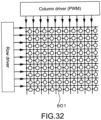
- the image forming unit may include a plurality of pixels arranged in a two-dimensional matrix. It should be noted that the image forming unit having such a configuration is referred to as an "image forming unit having a first configuration" for convenience sake.
- Examples of the image forming unit having a first configuration include: an image forming unit including a reflective spatial light modulation device and a light source; an image forming unit including a transmissive spatial light modulation device and a light source; and an image forming unit including a light-emitting element such as a light-emitting diode (LED), a semiconductor laser element, an organic EL (Electro Luminescence) element, or an inorganic EL element.
- LED light-emitting diode
- LED light-emitting diode
- LED light-emitting diode
- semiconductor laser element a semiconductor laser element
- organic EL (Electro Luminescence) element an organic EL (Electro Luminescence) element
- the spatial light modulation device examples include a light valve, for example, a transmissive or reflective liquid crystal display such as an LCOS (Liquid Crystal On Silicon), and a digital micromirror device (DMD).
- a light valve for example, a transmissive or reflective liquid crystal display such as an LCOS (Liquid Crystal On Silicon), and a digital micromirror device (DMD).
- the light source examples include the light-emitting element described above.
- the reflective spatial light modulation device may include a liquid crystal display and a polarizing beam splitter. The polarizing beam splitter reflects part of light from the light source and guides the light to the liquid crystal display, and causes part of the light reflected by the liquid crystal display to pass therethrough to guide the light to an optical system.
- Examples of the light-emitting element forming the light source may include a red light-emitting element, a green light-emitting element, a blue light-emitting element, and a white light-emitting element.
- red light, green light, and blue light that are output from the red light-emitting element, the green light-emitting element, and the blue light-emitting element, respectively may be used to achieve color mixture and uniformity in luminance by using a light pipe, to thus obtain white light.
- Examples of the light-emitting element may include a semiconductor laser element, a solid-state laser, and an LED.
- the number of pixels may be determined based on the specifications requested for the image display device and exemplified as specific values such as 320*240, 432*240, 640*480, 854*480, 1024*768, and 1920*1080.
- a collimating optical system that will be described later has a function of converting position information of a pixel into angle information of a light guide unit in the optical system. Examples of the collimating optical system include an optical system that includes a convex lens, a concave lens, a free-form-surface prism, and a hologram lens independently or in combination and has a positive optical power as a whole.
- the image forming unit may include a light source and a scanning unit configured to scan parallel light output from the light source. It should be noted that the image forming unit having such a configuration is referred to as an "image forming unit having a second configuration" for convenience sake.
- Examples of the light source in the image forming unit having a second configuration may include a light-emitting element, specifically, a red light-emitting element, a green light-emitting element, a blue light-emitting element, and a white light-emitting element.
- red light, green light, and blue light that are output from the red light-emitting element, the green light-emitting element, and the blue light-emitting element, respectively may be used to achieve color mixture and uniformity in luminance by using a light pipe, to obtain white light.
- Examples of the light-emitting element include a semiconductor laser element, a solid-state laser, and an LED.
- the number of pixels (virtual pixels) in the image forming unit having a second configuration may also be determined based on the specifications requested for the image display device and exemplified as specific values such as 320*240, 432*240, 640*480, 854*480, 1024*768, and 1920*1080. Further, in the case of color image display and in the case where the light source includes a red light-emitting element, a green light-emitting element, and a blue light-emitting element, for example, it is desirable to perform color composition by using a cross prism.
- Examples of the scanning unit may include MEMS (Micro Electro Mechanical Systems) including a micromirror that is rotatable in two-dimensional directions and horizontally and vertically scans light output from the light source, and a galvanometer mirror.
- MEMS Micro Electro Mechanical Systems
- a relay optical system that will be described next may be formed of a well-known relay optical system.
- the light that is changed into a plurality of parallel light beams in the optical system is input to the light guide plate.
- Such an optical system is an optical system, in which output light is assumed as parallel light, and which is referred to as a "parallel light outputting optical system" in some cases and specifically includes a collimating optical system or a relay optical system. In such a manner, being parallel light is requested based on the necessity to preserve light wavefront information obtained when those light beams are input to the light guide plate, even after those light beams are output from the light guide plate via the first deflection unit and the second deflection unit.
- a light output unit of the image forming unit may be provided at a spot (position) of the focal distance in the parallel light outputting optical system, for example.
- the parallel light outputting optical system has a function of converting position information of a pixel into angle information of the light guide unit in the optical system.
- Examples of the parallel light outputting optical system may include an optical system that includes a convex lens, a concave lens, a free-form-surface prism, and a hologram lens independently or in combination and has a positive optical power as a whole.
- a light shielding member having an opening may be disposed between the parallel light outputting optical system and the light guide plate so as to prevent undesired light from being output from the parallel light outputting optical system and input to the light guide plate.
- the following configuration may also be exemplified other than the combination of a backlight that emits white light as a whole and a liquid crystal display including red light-emitting pixels, green light-emitting pixels, and blue light-emitting pixels.
- An image forming unit A includes
- An image forming unit B includes
- An image forming unit C includes
- An image forming unit D which is an image forming unit for color display of a field sequential system, includes
- An image forming unit E which is also an image forming unit for color display of a field sequential system, includes
- An image forming unit F is an image forming unit for color display of a passive matrix type or an active matrix type in which an image is displayed by controlling the light-emitting/non-light-emitting states of first light-emitting elements, second light-emitting elements, and third light-emitting elements.
- An image forming unit G which is an image forming unit for color display of a field sequential system, includes
- the display device can have the following configuration: the light guide plate is disposed on the center of the observer's face in relation to the image forming unit as a whole; a connection member to connect two image display devices is further provided; the connection member is attached to one side of the frame, which faces the observer, at the central part located between two pupils of the observer; and a projected image of the connection member is included in a projected image of the frame.
- connection member is disposed between the observer and the frame, and, moreover, the projected image of the connection member is included in the projected image of the frame. In other words, when the head mounted display is viewed from the front of the observer, the connection member is hidden behind the frame. So, a high design quality can be given to the head mounted display.
- connection member be attached to the side of the frame, which faces the observer, at the central part of the front portion located between the two pupils of the observer.
- the central part corresponds to a bridge portion in normal eyeglasses.
- the two image display devices are connected to each other with the connection member.
- the image forming units are attached to both ends of the connection member such that the mounting state can be adjusted.
- the image forming units be located on the outside in relation to the pupils of the observer. In such a configuration, furthermore, it is desirable to satisfy:
- the center of the mounting portion of the image forming unit indicates a bisection point, along the axial direction of the frame, of a portion where a projected image of the image forming unit, which is obtained by projecting the image forming unit and the frame onto a virtual plane, is superimposed on a projected image of the frame, in the state where the image forming unit is attached to the connection member.
- the center of the connection member indicates a bisection point, along the axis direction of the frame, of a portion where the connection member is in contact with the frame, in the state where the connection member is attached to the frame.
- the length of the frame indicates the length of the projected image of the frame, in the case where the frame is curved. It should be noted that a projection direction is a direction vertical to the observer's face.
- the two image display devices are connected to each other with the connection member, and specifically, the following form can be adopted: two light guide plates are connected to each other with the connection member.
- the connection member is attached to such a light guide plate integrally produced.
- Such a form is also included in the form in which the two light guide plates are connected to each other with the connection member.
- the values of ⁇ ' and ⁇ ' are desirably set to the same as the values of ⁇ and ⁇ described above.
- the center of the image forming unit indicates a bisection point, along the axis direction of the frame, of a portion where a projected image of the image forming unit, which is obtained by projecting the image forming unit and the frame onto a virtual plane, is superimposed on a projected image of the frame, in the state where the image forming unit is attached to the light guide plate.
- connection member is substantially optional as long as the projected image of the connection member is included in the projected image of the frame.
- shape of the connection member include bar-like shapes and strip-like shapes.
- material forming the connection member include metals, alloys, plastics, and combinations thereof.
- a light beam that is output from the center of the image forming unit and passes through a nodal point on the image forming unit side of the optical system is referred to as a "central light beam", and a light beam in the central light beam, which is vertically input to the light guide unit, is referred to as a "central incident light beam”.
- a point at which the central incident light beam is input to the light guide unit is a light guide unit central point
- an axis that passes through the light guide unit central point and is parallel to the axis direction of the light guide unit is an X axis
- an axis that passes through the light guide unit central point and coincides with the normal line of the light guide unit is a Z axis.
- the horizontal direction in the display apparatus is a direction that is parallel to the X axis, and is hereinafter referred to as an "X-axis direction" in some cases.
- the optical system is disposed between the image forming unit and the light guide unit and changes light output from the image forming unit into parallel light. Subsequently, a light flux changed into the parallel light in the optical system is input to the light guide unit, guided to the light guide unit, and output from the light guide unit. Further, the central point of the first deflection unit is referred to as a "light guide unit central point".
- the light guide plate has two parallel surfaces (first surface and second surface) extending parallel to the axis of the light guide plate (the axis corresponds to a longitudinal direction or horizontal direction and corresponds to the X axis). It should be noted that the width direction of the light guide plate, which corresponds to a height direction or a vertical direction, corresponds to a Y axis. Assuming that a surface of the light guide plate, to which light is input, is an input surface of the light guide plate, and a surface of the light guide plate, from which light is output, is an output surface of the light guide plate, the input surface of the light guide plate and the output surface of the light guide plate may be each formed of the first surface. Alternatively, the input surface of the light guide plate may be formed of the first surface, and the output surface of the light guide plate may be formed of the second surface.
- the interference fringe of the diffraction grating member extends substantially parallel to the Y axis.
- Examples of the material forming the light guide plate may include glasses including an optical glass such as a quartz glass or BK7, and plastic materials (for example, PMMA (poly methyl methacrylate), polycarbonate resin, acrylic resin, amorphous polypropylene resin, and styrene resin including AS resin (acrylonitrile styrene copolymer)).
- glasses including an optical glass such as a quartz glass or BK7
- plastic materials for example, PMMA (poly methyl methacrylate), polycarbonate resin, acrylic resin, amorphous polypropylene resin, and styrene resin including AS resin (acrylonitrile styrene copolymer)
- the shape of the light guide plate is not limited to be a flat shape and may be a curved shape.
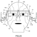
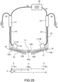
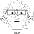
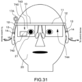
- the frame may include a front portion disposed on the front of the observer, and two temple portions turnably attached to both ends of the front portion via hinges. It should be noted that earpiece portions are attached to the tip ends of the respective temple portions.
- the image display device is attached to the frame. Specifically, for example, the image forming unit only needs to be attached to the temple portion. Further, a configuration in which the front portion and the two temple portions are incorporated can be adopted. In other words, when the whole of the display device according to the embodiment of the present disclosure is viewed, generally, the frame has substantially the same structure as that of normal eyeglasses.
- the materials forming the frame may be the same as materials forming normal eyeglasses, such as metals, alloys, plastics, and combinations thereof. Furthermore, a configuration in which nose pads are attached to the front portion can be adopted. In other words, when the whole of the display device according to the embodiment of the present disclosure is viewed, an assembled body of the frame and the nose pads has substantially the same structure as that of normal eyeglasses, except for the absence of a rim.
- the nose pads can have a well-known configuration and structure.
- each image forming unit includes a headphone portion and a headphone portion wire, which extends from each image forming unit, is extended from the tip end of the earpiece portion to the headphone portion through the inside of the temple portion and the earpiece portion.
- Examples of the headphone portion may include an inner ear type headphone portion and a canal type headphone portion. More specifically, it is desirable to adopt a form in which the headphone portion wire is extended to the headphone portion so as to run around the rear side of a pinna (auricle) from the tip end of the earpiece portion.
- a pinna auricle
- the frame may include a front portion disposed on the front of the observer, and two temple portions turnably attached to both ends of the front portion via hinges. It should be noted that the earpiece portions are attached to the tip ends of the respective temple portions.
- the dimming device is attached to the frame. Specifically, for example, the dimming device only needs to be attached to the front portion. Further, a configuration in which the front portion and the two temple portions are incorporated can be adopted. In other words, when the whole of the optical apparatus according to each of the first and second embodiments of the present disclosure is viewed, generally, the frame has substantially the same structure as that of normal eyeglasses.
- the dimming device is disposed instead of the lenses of the normal eyeglasses.
- the materials forming the frame may be the same as materials forming normal eyeglasses, such as metals, alloys, plastics, and combinations thereof.
- a configuration in which nose pads are attached to the front portion can be adopted.
- an assembled body of the frame and the nose pads has substantially the same structure as that of normal eyeglasses, except for the absence of a rim.
- the nose pads can have a well-known configuration and structure.
- an imaging device may be attached to the central part or an end of the frame or to the temple portion.
- the dimming device may be attached to the lenses of normal eyeglasses, or the lenses and the dimming device may be apposed.
- the display apparatus can form a head mounted display (HMD).
- HMD head mounted display
- the imaging device may be an imaging device having a well-known configuration and structure.
- the imaging device may include a solid-state imaging device, which has a CCD (Charge Coupled Device) or a CMOS (Complementary Metal Oxide Semiconductor) sensor, and a lens, for example.
- CCD Charge Coupled Device
- CMOS Complementary Metal Oxide Semiconductor
- the imaging device may be attached to the central part or end of the front portion or to the temple portion. Wires from the imaging device may be connected to one image display device (or image forming unit) via the front portion, for example, or may be included in the wires extending from the image display device (or image forming unit).
- a spatial area imaged by the imaging device may be displayed on the dimming device.
- the display apparatus including the various modifications described above may be available for displaying received electronic mails; for displaying various types of information in various sites on the Internet; for displaying various types of descriptions about how to drive, operate, maintain, or disassemble an observation target such as a variety of devices, and symbols, codes, marks, emblems, patterns, and the like; for displaying various types of descriptions about an observation target such as people and products, and symbols, codes, marks, emblems, patterns, and the like; for displaying moving and still images; for displaying subtitles in movies and the like; for displaying descriptions about video or closed captions in synchronization with video display; for displaying descriptions about an observation target in acting performances, Kabuki, Noh, Kyogen, Operas, music recitals, ballet, various types of theater plays, amusement parks, art museums, tourist attractions, tourist spots, and sightseeing signs, and the details of story, the progress of story, the background of story, and the like; and for displaying closed captions.
- the display apparatus may display characters as images related to an observation target whenever appropriate. Specifically, an image control signal is transmitted to the display apparatus and images are displayed on the display apparatus based on the progress of story in movies or in acting performances, based on a predetermined schedule and time allocation, in response to an operator's operation under the control of a computer or the like, for example.
- the observation targets such as various types of devices, people, and products may be imaged using an imaging device, and the imaged details may be analyzed in the display apparatus.
- the display apparatus may be able to display various types of descriptions created in advance about the observation targets such as various types of devices, people, and products.
- the display apparatus according to the embodiment of the present disclosure may be used as a stereoscopic display apparatus.
- a polarizer plate or a polarizer film may be detachably provided to the light guide unit, or bonded to the light guide unit, as appropriate.
- An image signal supplied to the image forming unit includes not only an image signal (for example, character data) but also luminance data (luminance information) on images to be displayed, chromaticity data (chromaticity information), or both the luminance data and the chromaticity data, for example.
- the luminance data may be luminance data corresponding to the luminance at a predetermined area including an observation target viewed through the light guide unit
- the chromaticity data may be chromaticity data corresponding to the chromaticity at the predetermined area including the observation target viewed through the light guide unit.
- the images to be displayed With an image signal including such luminance data on images, the images to be displayed become controllable in terms of luminance (brightness), and with an image signal including such chromaticity data on images, the images to be displayed become controllable in terms of chromaticity (color). Moreover, with an image signal including such luminance and chromaticity data on images, the images to be displayed become controllable in terms of both luminance (brightness) and chromaticity (color).
- the luminance data in use corresponds to the luminance at a predetermined area including an observation target viewed through the image display device
- the luminance data may be adjusted in value to increase the luminance of an image to be displayed, i.e., to make the image brighter when it is displayed, if the luminance at the predetermined area including the observation target viewed through the image display device is increased.
- the chromaticity data in use corresponds to the chromaticity at the predetermined area including the observation target viewed through the image display device
- the chromaticity data may be adjusted in value to obtain, roughly, a complementary color relationship between the chromaticity at the predetermined area including the observation target viewed through the image display device and the chromaticity of an image to be displayed.
- the complementary colors mean a pair of colors that are opposite to each other on the color circle, e.g., red and green, yellow and purple, and blue and orange.
- the complementary colors also mean a pair of colors that produces a color with reduced chroma when mixed in appropriate proportions, e.g., white for light, and black for objects.
- the complementary characteristics are not the same in terms of visual effects when the colors are placed next to each other, and when the colors are mixed together.
- the complementary colors are also referred to as antagonistic colors, contrast colors, or opposing colors. It should be noted that the expression of "opposing colors” directly identifies which colors are opposite to each other, whereas the expression of "complementary colors” identifies colors in a rather wider scope.
- the pair of complementary colors produces synergistic effects of enhancing their respective colors, and this is called complementary color harmony.
- Embodiment 1 relates to the display apparatus according to the embodiment of the present disclosure, and to the optical apparatus according to the second embodiment of the present disclosure.
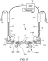
- Fig. 1 is a conceptual diagram of an image display device of Embodiment 1.
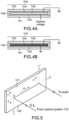
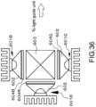
- Fig. 2 is a schematic diagram of the display apparatus (specifically, head mounted display (HMD)) of Embodiment 1 and the like when viewed from above.
- Fig. 3A is a schematic diagram of the display apparatus of Embodiment 1 when viewed from a lateral direction.
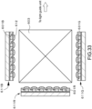
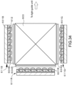
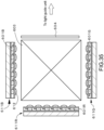
- Fig. 3B is a schematic diagram of a part including a light guide unit and a dimming device in the display apparatus of Embodiment 1 when viewed from the front.
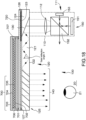
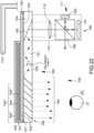
- FIGS. 4A and 4B are each a schematic cross-sectional diagram of the dimming device, schematically showing the behavior of the dimming device in the display apparatus of Embodiment 1.
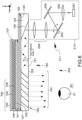
- Fig. 5 is a schematic diagram showing light propagation in a light guide plate that forms the image display device.
- the display apparatus of Embodiment 1 or Embodiments 2 to 14 that will be described later is a head mounted display (HMD) including
- the optical apparatus of Embodiment 1 or Embodiments 2 to 14 that will be described later includes
- control device 18 of the display apparatus which will be described later, is incorporated with a communication unit (receiving device), or the display apparatus includes a communication unit (receiving device) such as a mobile phone or a smartphone.
- a communication unit such as a mobile phone or a smartphone.
- information or data on an image displayed on the image display device or a signal to be received by the receiving device is recorded, stored, and saved in a so-called cloud computer or server, for example.
- cloud computer or server for example.
- various types of information or data, and signals can be transmitted and received or exchanged between the display apparatus and the cloud computer or the server, and signals based on various types of information or data, i.e., signals for displaying images on the image display device can be received.
- the receiving device can receive the signals.
- the display apparatus receives a signal for displaying an image on the image display device 100, 200, 300, 400, or 500, e.g., electronic mails and various types of information in a variety of sites on the Internet
- the light transmittance of the partial area 708 of the dimming device 700 is changed under the control of the control device 18, before the electronic mails and various types of information in a variety of sites on the Internet are displayed on the image display device 100, 200, 300, 400, or 500.
- the signals for displaying images on the image display device 100, 200, 300, 400, or 500 may be stored in the image display device, e.g., specifically in an image information storage unit 18A in the control device 18, and before images are displayed on the image display device 100, 200, 300, 400, or 500, the light transmittance of the partial area 708 of the dimming device 700 is changed under the control of the control device 18. Alternatively, the light transmittance of the dimming device 700 is changed based on the signal received by the receiving device.
- the change status of the light transmittance of the partial area 708 of the dimming device 700 may include a change from high light transmittance to low light transmittance, a change from low light transmittance to high light transmittance, and a change of high/low light transmittance in a short cycle (a change of light transmittance in blinking state).
- the dimming device 700 may be increased.
- the dimming device 700 may be operated to reduce the light transmittance, for example.
- the amount of outside light that passes through the dimming device 700 when the dimming device 700 does not operate is assumed to be "1"
- the dimming device 700 may be ON at all times, may be operated/not operated (turned ON/OFF) in response to an observer's command (operation), or may be OFF under normal conditions and may start operating in response to a signal for displaying an image on the image display device 100, 200, 300, 400, or 500.
- the display apparatus may further include a microphone, and may control the operation of the dimming device 700 in response to an audio input via the microphone, for example.
- the dimming device may be controlled to operate/not to operate in response to a command issued by an observer's voice.
- the display apparatus may further include an infrared light input/output unit, and using this infrared light input/output unit, may control the operation of the dimming device 700. That is, an observer's blinking may be detected using the infrared light input/output unit to control the dimming device 700 to operate/not to operate.
- Each of the image display devices 100, 200, 300, 400, and 500 of Embodiment 1 and Embodiments 2 to 14 that will be described later includes
- the image display device 100, 200, 300, 400, or 500 may be attached to the frame in a fixed manner or detachably.
- the optical system 112 or 254 is disposed between the image forming unit 111 or 211 and the light guide unit 120, 320, or 520.
- the light flux changed into the parallel light in the optical system 112 or 254 is input to the light guide unit 120, 320, or 520, guided therethrough, and output therefrom.
- the light guide unit 120, 320, or 520 is semi-transmissive (see-through). Specifically, portions of the light guide units, which are opposed to at least the both eyes of the observer 20 (more specifically, light guide plate 121 or 321 and second deflection unit 140 or 340 that will be described later), are semi-transmissive (see-through).
- Embodiment 1 or Embodiments 2 to 14 that will be described later, in a light beam (central incident light beam CL) that is output from the center of the image forming unit 111 or 211 and passes through a nodal point on the image forming unit side of the optical system 112 or 254, it is assumed that a point at which the central incident light beam vertically input to the light guide unit 120 or 320 is input to the light guide unit 120, 320, or 520 is a light guide unit central point O, an axis that passes through the light guide unit central point O and is parallel to the axis direction of the light guide unit 120, 320, or 520 is an X axis, and an axis that passes through the light guide unit central point O and coincides with the normal line of the light guide unit 120, 320, or 520 is a Z axis.
- a point at which the central incident light beam vertically input to the light guide unit 120 or 320 is input to the light guide unit 120, 320, or 520 is a light
- the central point of the first deflection unit 130 or 330 that will be described next is the light guide unit central point O.
- the central incident light beam CL that is output from the center of the image forming unit 111 or 211 and passes through a nodal point on the image forming unit side of the optical system 112 or 254 vertically impinges on the light guide plate 121 or 321.
- the central incident light beam CL is input to the light guide plate 121 or 321 at an incident angle of 0 degrees.
- the center of the displayed image coincides with a direction of a perpendicular of a first surface 122 or 322 of the light guide plate 121 or 321.
- Each of the light guide units 120 and 320 in Embodiment 1 and Embodiments 2 to 4 and 6 to 14 that will be described later includes
- the dimming device 700 configured to adjust the amount of outside light that comes from the outside is provided to the light guide unit 120, 320, or 520 on the side not provided with the image forming unit 111 or 211. Specifically, using an adhesive 707, the dimming device 700 as a kind of optical shutter is fixed to the light guide unit 120, 320, or 520, specifically, to a protection member (protection plate) 126 or 326 that protects the light guide plate 121 or 321 or a semi-transmissive mirror 520. The dimming device 700 is provided to the area of the light guide unit 120, 320, or 520 on the side opposite to the observer 20.
- protection member (protection plate) 126 or 326 is bonded to a second surface 123 or 323 of the light guide plate 121 or 321 using an adhesive 127 or 327, and the protection member (protection plate) 126 or 326 covers the first deflection unit 130 or 330 and the second deflection unit 140 or 340.
- the second deflection unit 140 or 340 is positioned in the projection image of the dimming device 700.
- the first deflection unit 130 and the second deflection unit 140 are disposed inside the light guide plate 121.
- the first deflection unit 130 reflects light input to the light guide plate 121
- the second deflection unit 140 transmits and reflects the light a plurality of times, the light being propagated inside the light guide plate 121 by total reflection.
- the first deflection unit 130 functions as a reflecting mirror
- the second deflection unit 140 functions as a semi-transmissive mirror.
- the first deflection unit 130 provided inside the light guide plate 121 is made of aluminum (Al) and is formed of a light reflecting film (a kind of mirror) that reflects the light input to the light guide plate 121.
- the second deflection unit 140 provided inside the light guide plate 121 is formed of a multi-layer lamination structure in which many dielectric lamination films are laminated.
- the dielectric lamination films includes a layer of TiO 2 (titanium dioxide) being a high dielectric material, and a layer of SiO 2 (silicon dioxide) being a low dielectric material, for example.
- TiO 2 titanium dioxide
- SiO 2 silicon dioxide
- the multi-layer lamination structure in which many dielectric lamination films are laminated is described in Japanese Unexamined Patent Application Publication No. 2005-521099 .
- Six dielectric lamination films are exemplarily shown in the figures, but this is not restrictive.
- a dielectric lamination film and another dielectric lamination film include therebetween a very thin layer made of the same material as the light guide plate 121.
- the parallel light input to the light guide plate 121 is totally reflected inside the light guide plate 121
- the parallel light input to the light guide plate 121 is reflected (or diffracted).
- the parallel light that is propagated inside the light guide plate 121 by total reflection is reflected (or diffracted) a plurality of times and output from the light guide plate 121 toward the pupil 21 of the observer 20 in the state of parallel light.
- the first deflection unit 130 may be formed by cutting out a portion 124 in which the first deflection unit 130 of the light guide plate 121 is to be provided, providing a slope on which the first deflection unit 130 is to be provided to the light guide plate 121, performing vacuum deposition on the slope to obtain a light reflecting film, and then bonding the cut-out portion 124 of the light guide plate 121 to the first deflection unit 130.
- the second deflection unit 140 may be formed by producing a multi-layer lamination structure in which many dielectric lamination films (formed by vapor deposition, for example) made of the same material as the light guide unit 121, e.g., glass, are laminated, cutting out a portion 125 in which the second deflection unit 140 of the light guide plate 121 is to be provided, to obtain a slope, bonding the multi-layer lamination structure to the slope, and shaping the outline by abrasion, for example.
- This allows the light guide unit 120 to be obtained, the light guide unit 120 being provided with the light guide plate 121 including the first and second deflection units 130 and 140.
- the light guide plate 121 or 321 that is made of an optical glass or a plastic material includes two parallel surfaces (first surface 122 or 322 and second surface 123 or 323) extending parallel to a light propagation direction (X axis) by internal total reflection of the light guide plate 121 or 321.
- the first surface 122 or 322 and the second surface 123 or 323 are opposed to each other.
- Parallel light is input from the first surface 122 or 322 that corresponds to a light input surface, and is output from the first surface 122 or 322 that corresponds to a light output surface, after being propagated inside the light guide plate 121 or 321 by total reflection.
- the light guide plate 121 or 321 is not limited to this configuration, and the light input surface may be formed of the second surface 123 or 323, and the light output surface may be formed of the first surface 122 or 322.
- the image forming unit 111 is an image forming unit having a first configuration and includes a plurality of pixels arranged in a two-dimensional matrix.
- the image forming unit 111 includes a reflective spatial light modulation device 150 and a light source 153 formed of a light-emitting diode that emits white light.
- the entire image forming unit 111 is housed in a casing 113 (in Fig. 1 , indicated by alternate long and short dash line).
- a casing 113 is provided with an opening (not shown), and light is output through the opening from the optical system (parallel light outputting optical system, collimating optical system) 112.
- the reflective spatial light modulation device 150 includes a liquid crystal display (LCD) 151 formed of an LCOS as a light valve, and a polarizing beam splitter 152.
- the polarizing beam splitter 152 reflects part of light from the light source 153 and guides the light to the liquid crystal display 151, and transmits part of the light reflected by the liquid crystal display 151 and guides the light to the optical system 112.
- the liquid crystal display 151 includes a plurality of (for example, 640*480) pixels (liquid crystal cells) arranged in a two-dimensional matrix.
- the polarizing beam splitter 152 has a well-known configuration and structure. Non-polarized light output from the light source 153 impinges on the polarizing beam splitter 152.
- a P-polarized light component passes therethrough and is output to the outside of the system.
- an S-polarized light component is reflected on the polarizing beam splitter 152, input to the liquid crystal display 151, reflected inside the liquid crystal display 151, and output from the liquid crystal display 151.
- light beams output from pixels for displaying "white” contain the P-polarized light component in a high proportion
- light beams output from pixels for displaying "black” contain the S-polarized light component in a high proportion.
- the P-polarized light component passes through the polarizing beam splitter 152 and is guided to the optical system 112.
- the S-polarized light component is reflected on the polarizing beam splitter 152 and returned back to the light source 153.
- the optical system 112 is formed of a convex lens, for example, and in order to generate parallel light, the image forming unit 111 (more specifically, liquid crystal display 151) is disposed at a spot (position) of the focal distance in the optical system 112.
- the frame 10 includes a front portion 11 disposed on the front of an observer 20, two temple portions 13 turnably attached to both ends of the front portion 11 via hinges 12, and earpiece portions (also referred to as tip cells, ear pieces, or ear pads) 14 attached to the tip ends of the respective temple portions 13. Further, nose pads (not shown in Fig. 2 ) are attached to the frame 10. In other words, basically, the assembled body of the frame 10 and the nose pads has substantially the same structure as that of normal eyeglasses. Furthermore, the casings 113 are detachably attached to the temple portions 13 with mounting members 19.
- the frame 10 is made of metal or plastic. It should be noted that each casing 113 may be attached to the temple portion 13 so as not to be detached with the mounting member 19.
- each casing 113 may be detachably attached to the temple portion of the frame of the eyeglasses owned by the observer with the mounting member 19.
- Each casing 113 may be attached to the outer side of the temple portion 13 or to the inner side of the temple portion 13.
- wires (signal line, power supply line, etc.) 15 extending from one image forming unit 111A are extended from the tip end of the earpiece portion 14 to the outside through the inside of the temple portion 13 and the earpiece portion 14 and are connected to a control device (control circuit or control unit) 18.
- each of the image forming units 111A and 111B includes a headphone portion 16.
- Headphone portion wires 16' which extend from the respective image forming units 111A and 111B, are extended from the tip ends of the earpiece portions 14 to the headphone portions 16 through the inside of the temple portions 13 and the earpiece portions 14.
- each headphone portion wire 16' is extended to the headphone portion 16 so as to run around the rear side of a pinna (auricle) from the tip end of the earpiece portion 14.
- a pinna auricle
- the wires (signal line, power supply line, etc.) 15 are connected to the control device (control circuit) 18 as described above.
- the control device 18 is provided with an image information storage unit 18A, for example.
- the control device 18 performs processing for image display.
- the control device 18 and the image information storage unit 18A may be each formed of a well-known circuit.
- An imaging device 17 including a solid-state imaging device and a lens (not shown) may be attached to a central part 11' of the front portion 11 with an adequate mounting member (not shown).
- the solid-state imaging device is formed of a CCD or a CMOS sensor.
- a signal supplied from the imaging device 17 is transmitted to, for example, the image forming unit 111A via a wire (not shown) extended from the imaging device 17.
- the dimming device 700 is formed of an optical shutter in which a light-transmission control material layer 705 is formed of a liquid crystal material layer.
- the dimming device 700 includes a transparent first substrate 701 opposed to the light guide unit 120, a transparent second substrate 703 opposed to the first substrate 701, a first electrode 702 and a second electrode 704 that are provided to the first substrate 701 and the second substrate 703, respectively, and the light-transmission control material layer 705 that is sealed between the first substrate 701 and the second substrate 703.
- the first substrate 701 and the second substrate 703 are each made of a plastic material.
- the first electrode 702 and the second electrode 704 are each formed of a transparent electrode made of indium tin oxide (ITO) and each formed by a combination of PVD such as sputtering and lifting off.
- the light-transmission control material layer 705 is formed of a liquid crystal material layer made of a TN (Twisted Nematic) liquid crystal material.
- the first electrode 702 and the second electrode 704 are provided by patterning, and the light transmittance of the partial area 708 of the dimming device 700 may be changed to be different from light transmittance of another area.
- the first electrode 702 and the second electrode 704 are connected to the control device 18 via connectors and wires (not shown).
- the two substrates 701 and 703 are sealed together at outer edge portions using a sealing agent 706.
- the first substrate 701 of the dimming device 700 and the protection member 126 (protecting the light guide plate 121) are bonded to each other by the adhesive 707. Further, polarizer films are affixed to the outer surfaces of the first substrate 701 and the second substrate 703, but those polarizer films are not shown.
- the first substrate 701 in the dimming device 700 is shorter than the light guide plate 121, and the first substrate 701 in the dimming device 700 is fixed to the protection member 126 using the adhesive 707.
- the adhesive 707 is provided at the outer edge portion of the first substrate 701. This is applicable also to other Embodiments to be described below.
- the light guide unit 120 and the dimming device 700 are disposed in this order from the observer's side.
- the light transmittance of the dimming device 700 may be controlled by a voltage applied to the first electrode 702 and the second electrode 704. Specifically, for example, when a voltage is applied to the first electrode 702 with the second electrode 704 being grounded, this causes a change of liquid crystal alignment in the liquid crystal material layer forming the light-transmission control material layer 705, so that the light transmittance of the liquid crystal material layer is changed (see Figs. 4A and 4B ).
- an observer may operate a control knob provided to the control device 18. That is, the observer may adjust the light transmittance of the dimming device 700 while observing images provided by the light guide unit 120 or 320.
- the display apparatus of Embodiment 1 since the light transmittance of the partial area of the dimming device is changed based on a signal for displaying an image on the image display device, this allows the observer to easily, reliably, and immediately recognize that an image is displayed. Alternatively, this allows the observer to easily and reliably recognize that an image is to be displayed. Alternatively, in the optical apparatus of Embodiment 1, since the light transmittance of the dimming device is changed based on a signal received by the receiving device, this allows the observer to easily, reliably, and immediately recognize that the receiving device receives a signal.
- the dimming device 700 is attached to the image display device 100, i.e., specifically, the dimmer unit 700 is attached to the light guide plate 121.
- the dimming device 700 may be attached to the frame 10 or to the casing 113.
- the dimming device may be attached to the frame without providing the image display device (see Fig. 30 , for example).
- the dimming device may include a first substrate, a second substrate opposed to the first substrate, a first electrode and a second electrode provided to the first substrate and the second substrate, respectively, and a light-transmission control material layer sealed between the first substrate and the second substrate, and at least one of the first substrate and the second substrate may be attached to the frame.
- the dimming device may be attached to the lenses of normal eyeglasses, or the lenses and the dimming device may be apposed and attached to the frame.
- Embodiment 2 is a modification of Embodiment 1.
- Fig. 6 shows a conceptual diagram of an image display device 200 in a display apparatus (head mounted display) of Embodiment 2
- an image forming unit 211 in Embodiment 2 is formed of an image forming unit having a second configuration.
- the image forming unit 211 includes a light source 251 and a scanning unit 253 configured to scan parallel light output from the light source 251. More specifically, the image forming unit 211 includes
- the light source 251 is formed of a light-emitting diode that emits white light.
- the light output from the light source 251 is input to the collimating optical system 252 having a positive optical power as a whole and is output as parallel light.
- the parallel light is reflected on a total reflection mirror 256.
- Horizontal scanning and vertical scanning are performed by the scanning unit 253 including a MEMS.
- the MEMS includes a micromirror that is rotatable in two-dimensional directions and with which the incident parallel light can be scanned in a two-dimensional manner.
- the parallel light is converted into a kind of two-dimensional image, resulting in the generation of virtual pixels (the number of pixels is, for example, the same as in Embodiment 1).
- the light from the virtual pixels passes through the relay optical system (parallel light outputting optical system) 254 formed of a well-known relay optical system, and a light flux changed into parallel light is input to the light guide unit 120.
- the light guide unit 120 to which the light flux changed into the parallel light in the relay optical system 254 is input, through which the light flux is guided, and from which the light flux is output, has the same configuration and structure as the light guide unit described in Embodiment 1, and thus detailed description thereof will be omitted. Further, as described above, the display apparatus of Embodiment 2 also has substantially the same configuration and structure as the display apparatus of Embodiment 1 except for the difference on the image forming unit 211, and thus detailed description thereof will be omitted.
- Embodiment 3 is also a modification of Embodiment 1.
- Fig. 7 is a conceptual diagram of an image display device 300 in a display apparatus (head mounted display) of Embodiment 3.
- Fig. 8 is a schematic cross-sectional diagram of a reflective volume holographic diffraction grating in a partially enlarged form.
- the image forming unit 111 is formed of the image forming unit having a first configuration, similarly in Embodiment 1.
- a light guide unit 320 is basically the same as the light guide unit 120 in Embodiment 1 in terms of structure and configuration except for differences in structures and configurations of the first deflection unit and the second deflection unit.
- the first deflection unit and the second deflection unit are disposed on a surface of the light guide plate 321 (specifically, on the second surface 323 of the light guide plate 321).
- the first deflection unit diffracts and reflects light input to the light guide plate 321
- the second deflection unit diffracts and reflects the light a plurality of times, the light being propagated inside the light guide plate 321 by total reflection.
- the first deflection unit and the second deflection unit are each a diffraction grating element, specifically a reflective diffraction grating element, and more specifically a reflective volume holographic diffraction grating.
- first deflection unit formed of a reflective volume holographic diffraction grating is referred to as a "first diffraction grating member 330" for convenience sake
- second deflection unit formed of a reflective volume holographic diffraction grating is referred to as a "second diffraction grating member 340" for convenience sake.
- the first diffraction grating member 330 and the second diffraction grating member 340 are each a laminate structure of a single diffraction grating layer.
- Each diffraction grating layer is made of photopolymer, and is provided with an interference pattern formed to correspond to one type of wavelength band (or wavelength).
- the diffraction grating layer is produced by a method in related art.
- the interference pattern formed on the diffraction grating layer (diffraction optical element) is constant in pitch, and is linear and parallel to the Y axis.
- the axes of the first diffraction grating member 330 and the second diffraction grating member 340 are both parallel to the X axis, and the normal lines thereto are parallel to the Z axis.
- Fig. 8 is a schematic cross-sectional diagram of a reflective volume holographic diffraction grating in a partially enlarged form.
- an interference fringe having an angle of inclination (slant angle) ⁇ is formed in the reflective volume holographic diffraction grating.
- the angle of inclination ⁇ means an angle formed by the surface of the reflective volume holographic diffraction grating and the interference fringe.
- the interference fringe is formed inside and over the surface of the reflective volume holographic diffraction grating. The interference fringe satisfies a Bragg's Law.
- the first diffraction grating member 330 is disposed on (bonded to) the second surface 323 of the light guide plate 321, and in order that the parallel light input from the first surface 322 to the light guide plate 321 is totally reflected inside the light guide plate 321, the first diffraction grating member 330 diffracts and reflects the parallel light input to the light guide plate 321.
- the second diffraction grating member 340 is disposed on (bonded to) the second surface 323 of the light guide plate 321, diffracts and reflects the parallel light a plurality of times, the parallel light being propagated inside the light guide plate 321 by total reflection, and outputs the parallel light as it is from the first surface 322 of the light guide plate 321.
- the parallel light is propagated inside the light guide plate 321 by total reflection and then output therefrom.
- the number of times the total reflection occurs until the light reaches the second diffraction grating member 340 differs depending on each angle of view. More specifically, in the parallel light that is input to the light guide plate 321, the number of reflections of the parallel light that is input at an angle of a direction approaching the second diffraction grating member 340 is smaller than the number of reflections of the parallel light that is input to the light guide plate 321 at an angle of a direction moving apart from the second diffraction grating member 340.
- parallel light that is diffracted and reflected in the first diffraction grating member 330 and is input to the light guide plate 321 at an angle of a direction approaching the second diffraction grating member 340 has a smaller angle formed together with the normal line of the light guide plate 321 when the light propagated inside the light guide plate 321 impinges on the internal surface of the light guide plate 321, than parallel light that is input to the light guide plate 321 at an angle of a direction opposite to the direction approaching the second diffraction grating member 340.
- the interference fringes formed in the second diffraction grating member 340 and the interference fringes formed in the first diffraction grating member 330 are symmetrical with respect to the virtual plane, which is vertical to the axis of the light guide plate 321.
- the surfaces of the first diffraction grating member 330 and the second diffraction grating member 340, which are not opposed to the light guide plate 321, are each covered with the protection member (protection plate) 326 so as to prevent the first diffraction grating member 330 and the second diffraction grating member 340 from being damaged.
- the light guide plate 321 and the protection member 326 are bonded to each other in their outer circumferential portions with the adhesive 327.
- the light guide plate 321 may be protected by attaching a transparent protection film to the first surface 322.
- the light guide plate 321 in Embodiment 4 that will be described later is basically the same as the light guide plate 321 described above in terms of structure and configuration.
- the display apparatus of Embodiment 3 has substantially the same structure and configuration as the display apparatus of Embodiment 1 except for the difference in the light guide unit 320, and thus detailed description thereof will be omitted.
- Embodiment 4 is a modification of Embodiment 3.
- Fig. 9 is a conceptual diagram of an image display device in a display apparatus (head mounted display) of Embodiment 4.
- the components in an image display device 400 of Embodiment 4, i.e., the light source 251, the collimating optical system 252, the scanning unit 253, the parallel light outputting optical system (relay optical system 254), and the like are in the same structure and configuration as those in Embodiment 2 (the image forming unit having a second configuration).
- a light guide unit 320 of Embodiment 4 has the same structure and configuration as the light guide unit 320 in Embodiment 3.
- the display apparatus of Embodiment 4 has substantially the same structure and configuration as the display apparatus of Embodiment 2 except for the differences described above, and thus detailed description thereof will be omitted.
- Embodiment 5 is also a modification of the image display devices of Embodiments 1 to 4.
- Fig. 10 is a schematic diagram of a display apparatus of Embodiment 5 when viewed from the front
- Fig. 11 is a schematic diagram of the display apparatus when viewed from above.
- a light guide unit 520 that forms an image display device 500 is formed of a semi-transmissive mirror.
- Light output from the image forming unit 111A or 111B is input to the semi-transmissive mirror and output therefrom toward a pupil 21 of an observer 20.
- Embodiment 5 has a structure in which the light output from the image forming unit 111A or 111B is propagated inside a transparent member 521 made of a glass plate, a plastic plate, or the like and input to the light guide unit 520 (semi-transmissive mirror), but may have a structure in which the light is propagated in air and input to the light guide unit 520.
- the image forming unit may be the image forming unit 211 described in Embodiment 2.
- Each of the image forming units 111A and 111B is attached to the front portion 11 with use of screws, for example. Further, the member 521 is attached to each of the image forming units 111A and 111B, the light guide unit 520 (semi-transmissive mirror) is attached to the member 521, and the dimming device 700 is attached to the light guide unit 520 (semi-transmissive mirror).
- the display apparatus of Embodiment 5 also has substantially the same configuration and structure as the display apparatuses of Embodiments 1 to 4 except for the difference described above, and thus detailed description thereof will be omitted.
- Embodiment 6 is also a modification of Embodiments 1 to 4.
- Fig. 12A is a schematic diagram of a display apparatus of Embodiment 6 when viewed from above
- Fig. 12B is a schematic diagram of a circuit for controlling an illumination sensor.
- the display apparatus of Embodiment 6 further includes a sensor 801 that measures the brightness in the outside environment. Based on a measurement result of the brightness in the outside environment obtained by the sensor (hereinafter, referred to as "first illumination sensor" for convenience sake) 801, light transmittance of a partial area of the dimming device 700 is changed.
- first illumination sensor for convenience sake
- the display apparatus of Embodiment 6 further includes the first illumination sensor (environmental illumination measurement sensor) 801 that measures the illumination in the environment where the display apparatus is disposed.
- the display apparatus controls the light transmittance of the dimming device 700 based on the measurement result of the first illumination sensor 801. Together with or separately from the control over the light transmittance, the display apparatus controls the luminance of images to be formed by the image forming unit 111 or 211 based on the measurement result of the first illumination sensor 801.
- the first illumination sensor 801 in the well-known structure and configuration may be provided to the outer end portion of the light guide unit 120 or 320, or to the outer end portion of the dimming device.
- the first illumination sensor 801 is connected to the control device 18 via connectors and wires (not shown).
- the control device 18 includes a circuit for controlling the first illumination sensor 801.
- This circuit for controlling the first illumination sensor 801 includes an illumination calculation circuit, a comparison calculation circuit, and an environmental illumination measurement sensor control circuit.
- the illumination calculation circuit calculates the illumination based on the measurement value provided by the first illumination sensor 801.
- the comparison calculation circuit compares the calculation result of the illumination calculation circuit, i.e., illumination value, with a standard value.
- the environmental illumination measurement sensor control circuit controls the dimming device 700 and/or the image forming unit 111 or 211 based on the value obtained by the comparison calculation circuit.
- Those circuits may be each formed of a well-known circuit.
- the light transmittance therein is controlled, and for controlling the image forming unit 111 or 211, the luminance of images to be formed thereby is controlled. It should be noted that the control over the light transmittance in the dimming device 700 and the control over the luminance of images formed by the image forming unit 111 or 211 may be executed separately or executed in correlation with each other.
- the dimming device 700 is adjusted to have the light transmittance of a predetermined value (first light transmittance) or lower.
- the dimming device 700 is adjusted to have the light transmittance of a predetermined value (second light transmittance) or higher.
- the first illumination measurement value may be 10 lux
- the first light transmittance may take any value in a range from 1% to 30% inclusive
- the second illumination measurement value may be 0.01 lux
- the second light transmittance may take any value in a range from 51% to 99% inclusive, for example.
- the first illumination sensor 801 in Embodiment 6 is applicable to the display apparatuses described in Embodiments 2 to 5.
- the first illumination sensor 801 may be formed of light-receiving elements provided to the imaging device for exposure measurement.
- the light transmittance of the dimming device is controlled based on the measurement result of the first illumination sensor (environmental illumination measurement sensor), and the luminance of images to be formed by the image forming unit is controlled also based on the measurement result of the first illumination sensor.
- the light transmittance of the dimming device is controlled based on the measurement result of the second illumination sensor (transmitted-light illumination measurement sensor), and the luminance of images to be formed by the image forming unit is controlled also based on the measurement result of the second illumination sensor. This can provide high-contrast to images viewed by an observer, and also optimize the surrounding conditions for observer's image observation while being dependent on the illumination in the ambient environment where the display apparatus is disposed.
- Embodiment 7 is also a modification of Embodiments 1 to 4.
- Fig. 13A is a schematic diagram of a display apparatus of Embodiment 7 when viewed from above
- Fig. 13B is a schematic diagram of a circuit for controlling an illumination sensor.
- the display apparatus of Embodiment 7 further includes a second illumination sensor (transmitted-light illumination measurement sensor) 802 that measures the illumination based on light that passes through the dimming device from the outside environment, that is, measures the illumination of environment light, i.e., whether the light is adjusted to have a desired value of illumination after passing through the dimming device.
- the measurement result of the second illumination sensor 802 is used as a basis to control the light transmittance of the dimming device 700. Together with or separately from the control over the light transmittance, the display apparatus controls the luminance of images to be formed by the image forming unit 111 or 211 based on the measurement result of the second illumination sensor 802.
- the second illumination sensor 802 in the well-known structure and configuration is disposed closer to the observer's side in relation to the light guide unit 120, 320, or 520. Specifically, the second illumination sensor 802 may be disposed to face the surface of the light guide unit 121 or 321 on the observer's side.
- the second illumination sensor 802 is connected to the control device 18 via connectors and wires (not shown).
- the control device 18 includes a circuit for controlling the second illumination sensor 802.
- This circuit for controlling the second illumination sensor 802 includes an illumination calculation circuit, a comparison calculation circuit, and a transmitted-light illumination measurement sensor control circuit.
- the illumination calculation circuit calculates the illumination based on the measurement value provided by the second illumination sensor 802.
- the comparison calculation circuit compares the calculation result of the illumination calculation circuit, i.e., illumination value, with a standard value.
- the transmitted-light illumination measurement sensor control circuit controls the dimming device 700 and/or the image forming unit 111 or 211 based on the value obtained by the comparison calculation circuit. Those circuits may be each formed of a well-known circuit. For controlling the dimming device 700, the light transmittance therein is controlled, and for controlling the image forming unit 111 or 211, the luminance of images to be formed thereby is controlled. It should be noted that the control over the light transmittance in the dimming device 700 and the control over the luminance of images formed by the image forming unit 111 or 211 may be executed separately or executed in correlation with each other.
- the dimming device may be adjusted in light transmittance while monitoring the value of the second illumination sensor 802.
- the second illumination sensor (transmitted-light illumination measurement sensor) 802 in Embodiment 7 is applicable to the display apparatuses described in Embodiments 2 to 4.
- the second illumination sensor 802 in Embodiment 7 may be combined with the first illumination sensor 801 in Embodiment 6 for use. If this is the case, with various tests, the control over the light transmittance in the dimming device 700 may be executed separately from or in correlation with the control over the luminance of images to be formed by the image forming unit 111 or 211.
- Embodiment 8 is a modification of Embodiments 1 to 7 and relates to the display apparatus according to the second embodiment of the present disclosure.
- Fig. 14 is a conceptual diagram of an image display device of Embodiment 8.
- Fig. 15 is a schematic diagram of the display apparatus (specifically, head mounted display (HMD)) of Embodiment 8 when viewed from above.
- Fig. 16A is a schematic diagram of the display apparatus when viewed from a lateral direction.
- Fig. 16B is a schematic diagram of a part including a light guide unit and a dimming device in the display apparatus when viewed from the front.
- a light shielding member is indicated by a dotted line.
- Fig. 16A a light shielding member is indicated by a dotted line.
- FIG. 17 is a conceptual diagram of a modification of the display apparatus of Embodiment 8.
- An example shown in Fig. 15 is a modification of the display apparatuses of Embodiments 1 to 4, and an example shown in Fig. 17 is a modification of the display apparatus of Embodiment 5.
- a light shielding member 710 is provided to an area of the light guide unit 120 where light output from the image forming unit 111A or 111B is input, specifically to an area where the first deflection unit 130 is provided.
- This light shielding member 710 is for shielding the light guide unit 120 from the outside light.
- the projection image of the light shielding member 710 toward the light guide unit 120 includes the area of the light guide unit 120 where the light output from the image forming unit 111A or 111B is input.
- the projection image of the light shielding member 710 toward the light guide unit 120 also includes the projection image of the end of the dimming device 700 toward the light guide unit 120.
- the light shielding member 710 is provided to the light guide unit 120 on the side not provided with the image forming unit 111A or 111B, and is provided with a distance from the light guide unit 120.
- the light shielding member 710 is made of a non-transparent plastic material, for example.
- This light shielding member 710 is integrally extended from the casing 113 of the image display device 111A or 111B, or is attached to the casing 113 of the image forming unit 111A or 111B.
- the light shielding member 710 is integrally extended from the frame 10, or is attached to the frame 10.
- the light shielding member 710 is integrally extended from the casing 113 of the image forming unit 111A or 111B.
- the light shielding member is provided to an area of the light guide unit where light output from the image forming unit is input.
- This light shielding member is for shielding the light guide unit from the outside light. Therefore, even if the operation of the dimming device changes the amount of incoming outside light, this does not cause degradation in image quality on the display apparatus with no undesired stray light because no outside light enters the area of the light guide unit where light output from the image forming unit is input, i.e., the first deflection unit 130, in the first place.
- Embodiment 9 is a modification of Embodiment 8. As shown in a conceptual diagram of Fig. 18 , unlike the display apparatus of Embodiment 8, a display apparatus of Embodiment 9 includes a light shielding member 720 in a portion of the light guide unit 120 on the side not provided with the image forming unit 111A or 111B. Specifically, the light shielding member 720 may be formed by printing on the light guide unit 120 (specifically on the inner surface of the protection member 126) using a non-transparent ink. Except for the above, the display apparatus of Embodiment 9 has the same structure and configuration as the display apparatus of Embodiment 8, and thus detailed description thereof will be omitted. The light shielding member 720 of Embodiment 9 may be combined with the light shielding member 710 of Embodiment 8 for use. The light shielding member 720 may be formed on the outer surface of the protection member 126.
- Embodiment 10 is also a modification of Embodiment 8. As shown in a conceptual diagram of Fig. 19 or 20 , unlike the display apparatuses of Embodiments 8 and 9, a display apparatus of Embodiment 10 includes a light shielding member 730 in the dimming device 700. Specifically, the light shielding member 730 may be formed by printing on the dimming device 700 using a non-transparent ink. In the example of Fig. 19 , the light shielding member 730 is formed on the outer surface of the first substrate 701 in the dimming device 700, and in the example of Fig. 20 , the light shielding member 730 is formed on the inner surface of the first substrate 701 in the dimming device 700.
- the display apparatus of Embodiment 10 has the same structure and configuration as the display apparatus of Embodiment 8, and thus detailed description thereof will be omitted.
- the light shielding member 730 of Embodiment 10 may be combined with the light shielding member 710 of Embodiment 8 for use, the light shielding member 730 of Embodiment 10 may be combined with the light shielding member 720 of Embodiment 9 for use, or the light shielding member 730 of Embodiment 10 may be combined with the light shielding members 710 and 720 of Embodiments 8 and 9.
- Embodiment 11 is a modification of Embodiments 1 to 10.
- the light-transmission control material layer 705 is formed of a liquid crystal material layer.
- a light-transmission control material layer 705' is an optical shutter formed of an inorganic EL material layer.
- the inorganic EL material layer is made of tungstic oxide (WO 3 ).
- a first substrate 701' and a second substrate 703' are each a transparent glass substrate such as soda lime glass or super white glass, and the second substrate 703' is made thinner than the first substrate 701'.
- the second substrate 703' is formed with the thickness of 0.2 mm
- the first substrate 701' is formed with the thickness of 0.4 mm.
- the display apparatus of Embodiment 11 has the same structure and configuration as the display apparatuses of Embodiments 8 to 10, and thus detailed description thereof will be omitted.
- the first substrate 701' in the dimming device 700' is bonded to the protection member 126 using the adhesive 707 similarly to Embodiment 8.
- Embodiment 12 relates to the display apparatus according to the first embodiment of the present disclosure and is a modification of Embodiment 11. As shown in a conceptual diagram of Fig. 22 , in a display apparatus of Embodiment 12, a dimming device 700" includes
- the first substrate 701" that forms the dimming device 700" also serves as a constituent member (the protection member 126) of the light guide unit 120. This reduces the total weight of the display apparatus so that this does not give discomfort to a user of the display apparatus.
- the display apparatus of Embodiment 12 has the same structure and configuration as the display apparatus of Embodiment 11, and thus detailed description thereof will be omitted.
- the light shielding member in the display apparatus of Embodiment 12 has the same structure and configuration as the dimming device in each of the display apparatuses of Embodiments 8 to 10, and thus detailed description thereof will be omitted.
- Embodiment 13 is a modification of Embodiments 1 to 12.
- Fig. 23 is a schematic diagram of a head mounted display of Embodiment 13 when viewed from the front.
- Fig. 24 is a schematic diagram of the head mounted display of Embodiment 13 (in a state assuming that a frame is removed) when viewed from the front.
- Fig. 25 is a schematic diagram of the head mounted display of Embodiment 13 when viewed from above.
- Fig. 26 is a diagram showing a state where the head mounted display of Embodiment 13 is mounted onto the head of an observer 20 when viewed from above. It should be noted that Fig. 26 shows only the image display devices and the illustration of the frame is omitted for convenience sake.
- the image display device is typified by the image display device 100, but needless to say, the image display device 200, 300, 400, or 500 can be applied to the image display device.
- the illustration of the dimming device 700 is omitted.
- the head mounted display of Embodiment 13 further includes a connection member 160 that connects the two image display devices 100.
- the connection member 160 is attached to one side of a frame 10, which faces the observer, at a central part 10C located between two pupils 21 of the observer 20 (i.e., attached between the observer 20 and the frame 10), with use of screws (not shown), for example.
- a projected image of the connection member 160 is included in a projected image of the frame 10. In other words, when the head mounted display is viewed from the front of the observer 20, the connection member 160 is hidden behind the frame 10, and the connection member 160 is not visually recognized.
- the two image display devices 100 are connected to each other with the connection member 160, but specifically, the image forming units 111A and 111B are stored in respective casings 113, and the casings 113 are attached to both ends of the connection member 160 such that the mounting state can be adjusted.
- the image forming units 111A and 111B are located on the outside in relation to the pupils 21 of the observer 20.
- the mounting of the image forming units (specifically, image forming units 111A and 111B) to both ends of the connection member 160 is specifically performed as follows, for example: three through-holes (not shown) are provided at three positions of each of the ends of the connection member; tapped hole portions (screw-engagement portions (not shown)) corresponding to the through-holes are provided to the image forming units 111A and 111B; and screws (not shown) are inserted into the respective through-holes and screwed into the hole portions provided to the image forming units 111A and 111B.
- a spring is inserted in advance between each screw and a corresponding hole portion.
- connection members 160 and 170 are hatched.
- the connection member 160 is attached to the central part 10C of the frame 10 that is located between the two pupils 21 of the observer 20.
- the central part 10C corresponds to the bridge portion in normal eyeglasses.
- nose pads 10' are attached to the side of the connection member 160, which faces the observer 20. It should be noted that in Figs. 25 and 29 , the illustration of the nose pads 10' is omitted.
- the frame 10 and the connection member 160 are made of metal or plastic, and the shape of the connection member 160 is a curved bar-like shape.
- the connection member 160 connects the two image display devices 100, and the connection member 160 is attached to the central part 10C of the frame 10 that is located between the two pupils 21 of the observer 20.
- each of the image display devices 100 is not directly attached to the frame 10. So, when the frame 10 is mounted onto the head of the observer 20, the temple portions 13 are expanded outwards. As a result, even if the frame 10 is deformed, such a deformation of the frame 10 does not cause a displacement (positional change) of the image forming unit 111A or 111B, or causes little displacement, if any. For that reason, the angle of convergence of left and right images can be certainly prevented from being changed.
- the design, color, and the like of the frame 10 can be freely selected according to the observer's preference, and thus there are few restrictions imposed on the design of the frame 10 and the degree of freedom on a design basis is high.
- the connection member 160 is hidden behind the frame 10. So, a high design quality can be given to the head mounted display.
- Embodiment 14 is a modification of Embodiment 13.
- Fig. 27 is a schematic diagram of a head mounted display of Embodiment 14 when viewed from the front
- Fig. 28 is another schematic diagram of the head mounted display of Embodiment 14 (in a state assuming that a frame is removed) when viewed from the front
- Fig. 29 is a schematic diagram of the head mounted display of Embodiment 14 when viewed from above.
- a bar-like connection member 170 connects the two light guide units 120 instead of connecting the two image forming units 111A and 111B. It should be noted that the two light guide units 120 may be integrally produced and the connection member 170 may be attached to such a light guide unit 120 integrally produced.
- connection member 170 is attached to the frame 10 at a central part 10C located between two pupils 21 of the observer 20 with use of screws, for example.
- the frame 10 and the image display devices have the same structures and configurations as the frame 10 and the image display devices described in Embodiment 13, and thus detailed description thereof will be omitted.
- the head mounted display of Embodiment 14 also has substantially the same structure and configuration as the head mounted display of Embodiment 13 except for the differences described above, and thus detailed description thereof will be omitted.
- Embodiment 15 represents an embodiment according to the present invention and relates to the optical apparatus according to the first embodiment of the present disclosure.
- Figs. 30 and 31 are each a schematic diagram of an optical apparatus and the like of Embodiment 15 when viewed from the front.
- the optical apparatus of Embodiment 15 includes
- the outer edge of the spatial area imaged by the imaging device 17A is displayed in the form of a frame 741 in the dimming device.
- light transmittance of the area 742 of the dimming device that corresponds to the spatial area imaged by the imaging device 17A may be made lower or higher than light transmittance of an area 743 of the dimming device that corresponds to the outside of the spatial area imaged by the imaging device 17A.
- the optical apparatus of Embodiment 15 may further include a dimming-device-controlling device, and the positions of the areas 741 and 742 of the dimming device that each correspond to the spatial area imaged by the imaging device may be corrected by the dimming-device-controlling device.
- the optical apparatus of Embodiment 15 includes a mobile phone or a smartphone, for example, or when the optical apparatus is combined with a mobile phone, a smartphone, or a personal computer, the spatial area imaged by the imaging device 17A may be displayed on the mobile phone, the smartphone, or the personal computer.
- the area 741 or 742 of the dimming device that corresponds to the spatial area imaged by the imaging device 17A is moved/turned or enlarged/contracted using the dimming-device-controlling device, which can be substituted by the mobile phone, the smartphone, or the personal computer.
- the difference between the spatial area displayed on the mobile phone, the smartphone, or the personal computer and the area 741 or 742 of the dimming device that corresponds to the spatial area imaged by the imaging device 17A may be eliminated.
- the spatial area imaged by the imaging device is displayed on the dimming device. This allows the observer to easily and reliably recognize which part of the outside is imaged by the imaging device.
- the display apparatuses and the optical apparatuses described in Embodiments 1 to 14 are each applicable to the optical apparatus of Embodiment 15. Further, the optical apparatus according to the second embodiment of the present disclosure is also applicable to the optical apparatus of Embodiment 15.
- the optical apparatus may include a receiving device that is similar to that described in Embodiment 1, and based on a signal received by the receiving device, light transmittance of the area 741 or 742 of the dimming device 740 may be changed, for example.
- a surface relief hologram (see U.S. Patent Application No. 20040062505A1 ) may be disposed on a light guide plate.
- the diffraction grating element may be formed of the transmissive diffraction grating element.
- the first or second deflection unit may be formed of a reflective diffraction grating element, and the remaining one may be formed of a transmissive diffraction grating element.
- the diffraction grating element may be a reflective blazed diffraction grating element.
- the dimming device may be detachably provided in an area from which the light guide unit emits light.
- the dimming device may be attached to the light guide unit using a screw made of transparent plastic, for example.
- the dimming device may be then connected to a control circuit via connectors and wires. This control circuit is for controlling the light transmittance of the dimming device, and is provided in the control device 18 that controls the image forming unit, for example.
- an optical shutter may be used by application of electrodeposition/dissociation that occurs in response to the reversible oxidation reduction of metal, e.g., silver particles.
- metal e.g., silver particles.
- Ag + (silver) and I - (iodine) are dissolved in advance in an organic solvent, and Ag is precipitated by reduction of Ag + through appropriate voltage application to electrodes so that the dimming device is reduced in light transmittance.
- Ag is oxidized and dissolved as Ag + , so that the dimming device is increased in light transmittance.
- an optical shutter may be used by application of color change of substance that occurs in response to the oxidation reduction of an electrochromic material.
- first and second electrodes are provided, and first and second electrochromic material layers are sandwiched between the first and second electrodes.
- the first electrochromic material layer is formed of a prussian blue metal complex, for example
- the second electrochromic material layer is formed of a nickel-substituted prussian blue metal complex, for example.
- an optical shutter may be used which controls the light transmittance by electrowetting.
- first and second electrodes are provided, and a gap between the first and second electrodes is filled with insulating first liquid and conductive second liquid. By voltage application between the first and second electrodes, the interface between the first liquid and the second liquid is changed in shape, e.g., from being flat to being bent, thereby controlling the light transmittance.
- the image forming unit 111 or 211 is described as one that displays a monochrome (for example, green) image, but the image forming unit 111 or 211 can also display a color image.
- the light source only needs to be formed of a light source that outputs red light, green light, and blue light, for example.
- red light, green light, and blue light that are output from a red light-emitting element, a green light-emitting element, and a blue light-emitting element, respectively, may be used to achieve color mixture and uniformity in luminance by using a light pipe, to thus obtain white light.
- the following configuration may also be exemplified other than the combination of a backlight that emits white light as a whole and a liquid crystal display including red, green, and blue light-emitting pixels.
- an active matrix type image forming unit including a light-emitting panel on which light-emitting elements 601 formed of semiconductor laser elements are arranged in a two-dimensional matrix.
- the active matrix type image forming unit the light-emitting/non-light-emitting states of the light-emitting elements 601 is controlled and the light-emitting states of the light-emitting elements 601 are directly observed, and thus an image is displayed.
- Light output from this image forming unit is input to the light guide plate 121 via the collimating optical system 112.
- the light-emitting element is formed of the semiconductor laser element.
- an image forming unit for color display including
- an image forming unit including, as shown in a conceptual diagram of Fig. 34 , light-emitting panels 611R, 611G, and 611B on which light-emitting elements 601R, 601G, and 601B are arranged in a two-dimensional matrix, respectively.
- the passages/non-passages of light beams output from the light-emitting panels 611R, 611G, and 611B are controlled by light passage control devices 604R, 604G, and 604B, and the light beams are input to a dichroic prism 603.
- the optical paths of those light beams are collected into one optical path and input to the light guide plate 121 via the collimating optical system 112.
- an image forming unit including, as shown in a conceptual diagram of Fig. 35 , light-emitting panels 611R, 611G, and 611B on which light-emitting elements 601R, 601G, and 601B are arranged in a two-dimensional matrix, respectively.
- Light beams output from the light-emitting panels 611R, 611G, and 611B are input to a dichroic prism 603, and the optical paths of those light beams are collected into one optical path.
- the passages/non-passages of the light beams output from the dichroic prism 603 are controlled by a light passage control device 604, and the light beams are input to the light guide plate 121 via the collimating optical system 112.
- an image forming unit including: a light-emitting element 601R that emits red light; a light passage control device (for example, liquid crystal display 604R) as a kind of light valve, configured to control the passage/non-passage of output light output from the light-emitting element 601R that emits red light; a light-emitting element 601G that emits green light; a light passage control device (for example, liquid crystal display 604G) as a kind of light valve, configured to control the passage/non-passage of output light output from the light-emitting element 601G that emits green light; a light-emitting element 601B that emits blue light; a light passage control device (for example, liquid crystal display 604B) as a kind of light valve, configured to control the passage/non-passage of output light output from the light-emitting element 601B that emits green light; light leading members 602 configured to lead the light
Landscapes
- Physics & Mathematics (AREA)
- General Physics & Mathematics (AREA)
- Optics & Photonics (AREA)
- Engineering & Computer Science (AREA)
- Computer Hardware Design (AREA)
- Theoretical Computer Science (AREA)
- Astronomy & Astrophysics (AREA)
- Spectroscopy & Molecular Physics (AREA)
- Instrument Panels (AREA)
- Devices For Indicating Variable Information By Combining Individual Elements (AREA)
Applications Claiming Priority (1)
| Application Number | Priority Date | Filing Date | Title |
|---|---|---|---|
| JP2014053191A JP6391952B2 (ja) | 2014-03-17 | 2014-03-17 | 表示装置及び光学装置 |
Publications (3)
| Publication Number | Publication Date |
|---|---|
| EP2930552A2 EP2930552A2 (en) | 2015-10-14 |
| EP2930552A3 EP2930552A3 (en) | 2016-01-06 |
| EP2930552B1 true EP2930552B1 (en) | 2023-06-14 |
Family
ID=52423606
Family Applications (1)
| Application Number | Title | Priority Date | Filing Date |
|---|---|---|---|
| EP15152708.2A Active EP2930552B1 (en) | 2014-03-17 | 2015-01-27 | Display apparatus and optical apparatus |
Country Status (4)
| Country | Link |
|---|---|
| US (1) | US10642040B2 (zh) |
| EP (1) | EP2930552B1 (zh) |
| JP (1) | JP6391952B2 (zh) |
| CN (1) | CN104932102B (zh) |
Families Citing this family (48)
| Publication number | Priority date | Publication date | Assignee | Title |
|---|---|---|---|---|
| JP5434848B2 (ja) | 2010-08-18 | 2014-03-05 | ソニー株式会社 | 表示装置 |
| JP5780129B2 (ja) | 2011-11-22 | 2015-09-16 | ソニー株式会社 | 光ビーム伸長装置、画像表示装置及び光学装置 |
| JP5879973B2 (ja) | 2011-11-30 | 2016-03-08 | ソニー株式会社 | 光反射部材、光ビーム伸長装置、画像表示装置及び光学装置 |
| JP6003903B2 (ja) | 2012-01-24 | 2016-10-05 | ソニー株式会社 | 表示装置 |
| JP6145966B2 (ja) | 2012-05-09 | 2017-06-14 | ソニー株式会社 | 表示装置 |
| JP6394393B2 (ja) | 2013-01-10 | 2018-09-26 | ソニー株式会社 | 画像表示装置、画像生成装置及び透過型空間光変調装置 |
| JP6123342B2 (ja) | 2013-02-20 | 2017-05-10 | ソニー株式会社 | 表示装置 |
| US10527859B2 (en) | 2013-04-11 | 2020-01-07 | Sony Corporation | Image display device and display apparatus |
| WO2014168010A1 (ja) | 2013-04-11 | 2014-10-16 | ソニー株式会社 | 画像表示装置及び表示装置 |
| JP6367529B2 (ja) | 2013-06-25 | 2018-08-01 | ソニー株式会社 | 表示装置、表示制御方法、表示制御装置、および電子機器 |
| US10302946B2 (en) | 2013-07-04 | 2019-05-28 | Sony Corporation | Display apparatus |
| CN104737060B (zh) | 2013-07-16 | 2018-12-11 | 索尼公司 | 显示装置 |
| US9952435B2 (en) | 2013-07-16 | 2018-04-24 | Sony Corporation | Display apparatus having curved image forming apparatus |
| JP6314518B2 (ja) | 2014-02-10 | 2018-04-25 | ソニー株式会社 | 画像表示装置及び表示装置 |
| JP2015148782A (ja) | 2014-02-10 | 2015-08-20 | ソニー株式会社 | 画像表示装置及び表示装置 |
| JP6201836B2 (ja) | 2014-03-14 | 2017-09-27 | ソニー株式会社 | 光学装置及びその組立方法、ホログラム回折格子、表示装置並びにアライメント装置 |
| JP2015184560A (ja) | 2014-03-25 | 2015-10-22 | ソニー株式会社 | 導光装置、画像表示装置及び表示装置 |
| JP2015184561A (ja) | 2014-03-25 | 2015-10-22 | ソニー株式会社 | 導光装置、画像表示装置及び表示装置 |
| US9568789B2 (en) * | 2014-11-19 | 2017-02-14 | Omnivision Technologies, Inc. | Panel carrier for a liquid crystal on silicon panel and method for electrically interconnecting same |
| US9633626B2 (en) * | 2015-03-12 | 2017-04-25 | Visteon Global Technologies, Inc. | Adjusting an electronic display based on gaze tracking |
| JP6844216B2 (ja) * | 2015-11-25 | 2021-03-17 | 株式会社リコー | 視認システム |
| FR3046850B1 (fr) | 2016-01-15 | 2018-01-26 | Universite De Strasbourg | Guide optique ameliore et systeme optique comportant un tel guide optique |
| CN107037610A (zh) * | 2016-02-04 | 2017-08-11 | 姜莹 | 隐形摄像眼镜 |
| EP3281909A1 (en) * | 2016-08-08 | 2018-02-14 | Essilor International | Projector configured to project an image onto a surface and portable device comprising such projector |
| TWI622803B (zh) * | 2016-08-30 | 2018-05-01 | 廣達電腦股份有限公司 | 頭戴式顯示裝置 |
| CN107919096A (zh) * | 2016-10-11 | 2018-04-17 | 中兴通讯股份有限公司 | 一种控制方法和头戴式设备 |
| US10534185B1 (en) | 2017-02-14 | 2020-01-14 | Facebook Technologies, Llc | Multi-planar display with waveguide and lens stacks |
| CN118311774A (zh) * | 2017-06-26 | 2024-07-09 | 京东方科技集团股份有限公司 | 显示系统和图像显示方法 |
| US10895746B1 (en) | 2017-08-07 | 2021-01-19 | Facebook Technologies, Llc | Expanding field-of-view in direct projection augmented reality and virtual reality systems |
| CN107422474B (zh) * | 2017-08-14 | 2020-12-01 | 京东方科技集团股份有限公司 | 一种光束扩展结构及光学显示模组 |
| JP6958106B2 (ja) * | 2017-08-21 | 2021-11-02 | セイコーエプソン株式会社 | 偏向装置、表示装置および偏向装置の製造方法 |
| US10534209B1 (en) * | 2017-08-21 | 2020-01-14 | Facebook Technologies, Llc | Liquid crystal structure for controlling brightness uniformity in a waveguide display |
| CN111373291A (zh) | 2017-11-21 | 2020-07-03 | Agc株式会社 | 光学玻璃、光学部件和光学设备 |
| CN107966819A (zh) * | 2017-12-27 | 2018-04-27 | 北京灵犀微光科技有限公司 | 波导显示装置 |
| US10942355B2 (en) * | 2018-01-22 | 2021-03-09 | Facebook Technologies, Llc | Systems, devices, and methods for tiled multi-monochromatic displays |
| US10613332B1 (en) | 2018-02-15 | 2020-04-07 | Facebook Technologies, Llc | Near-eye display assembly with enhanced display resolution |
| KR102084723B1 (ko) * | 2018-06-27 | 2020-03-04 | (주)비젼에이드 | 플라스틱 엘시디 셰이드를 구비한 증강현실 및 가상현실 겸용 스마트 글라스 디스플레이 장치 |
| WO2020056384A1 (en) | 2018-09-14 | 2020-03-19 | Magic Leap, Inc. | Systems and methods for external light management |
| JP7155815B2 (ja) * | 2018-09-27 | 2022-10-19 | セイコーエプソン株式会社 | 頭部装着型表示装置 |
| US11899235B2 (en) * | 2018-12-05 | 2024-02-13 | Elbit Systems Ltd. | Display illumination optics |
| CN110286538B (zh) * | 2019-06-28 | 2022-05-24 | Oppo广东移动通信有限公司 | 显示方法、显示装置、头戴式显示装置和存储介质 |
| CN110361866A (zh) * | 2019-07-11 | 2019-10-22 | Oppo广东移动通信有限公司 | 一种透射光强可调的头戴显示设备 |
| DE102019212989B3 (de) * | 2019-08-29 | 2021-01-14 | Audi Ag | Kameravorrichtung zum Erzeugen von räumlich darstellenden Bilddaten einer Umgebung |
| CN110927969A (zh) * | 2019-12-09 | 2020-03-27 | 京东方科技集团股份有限公司 | 光学显示系统和显示装置 |
| JP7453403B2 (ja) | 2020-03-02 | 2024-03-19 | カール ツアイス メディテック アクチエンゲゼルシャフト | ヘッドマウント可視化システム |
| CN111432132B (zh) * | 2020-05-09 | 2022-11-08 | 深圳传音控股股份有限公司 | 一种图像获取方法、装置及介质 |
| KR20220018107A (ko) * | 2020-08-05 | 2022-02-15 | 삼성디스플레이 주식회사 | 표시 장치 |
| US11662525B1 (en) * | 2021-12-09 | 2023-05-30 | Visera Technologies Company Ltd. | Optical system |
Citations (3)
| Publication number | Priority date | Publication date | Assignee | Title |
|---|---|---|---|---|
| JP2007264324A (ja) * | 2006-03-28 | 2007-10-11 | Brother Ind Ltd | 画像表示装置 |
| US20130257691A1 (en) * | 2012-04-02 | 2013-10-03 | Seiko Epson Corporation | Head-mount type display device |
| US20140071294A1 (en) * | 2012-09-12 | 2014-03-13 | Bae Systems Information And Electronic Systems Integration Inc. | Face mounted extreme environment thermal sensor system |
Family Cites Families (101)
| Publication number | Priority date | Publication date | Assignee | Title |
|---|---|---|---|---|
| JPS5726822A (en) * | 1980-06-10 | 1982-02-13 | Seiko Epson Corp | Dimming spectacles |
| JPH01188826A (ja) | 1988-01-22 | 1989-07-28 | Fujitsu Ltd | 光シャッタ |
| JPH024212A (ja) | 1988-06-23 | 1990-01-09 | Stanley Electric Co Ltd | 液晶シャッタ素子 |
| US5224198A (en) | 1991-09-30 | 1993-06-29 | Motorola, Inc. | Waveguide virtual image display |
| JPH0888815A (ja) | 1994-09-19 | 1996-04-02 | Olympus Optical Co Ltd | 映像表示システム |
| JPH08160344A (ja) | 1994-12-05 | 1996-06-21 | Olympus Optical Co Ltd | 頭部装着式映像表示装置 |
| JP3630746B2 (ja) * | 1994-12-05 | 2005-03-23 | キヤノン株式会社 | 画像観察装置 |
| JPH10126711A (ja) | 1996-10-17 | 1998-05-15 | Olympus Optical Co Ltd | 頭部搭載型画像表示装置 |
| JPH10319240A (ja) | 1997-05-22 | 1998-12-04 | Fuji Xerox Co Ltd | ヘッドマウンテッドディスプレイ |
| BR9906400A (pt) | 1998-04-28 | 2000-09-26 | Citizen Watch Co Ltd | Dispositivo indicador de cristal lìquido colorido do tipo refletor |
| JP2000171750A (ja) * | 1998-12-03 | 2000-06-23 | Sony Corp | ヘッドマウントディスプレイ、表示方法、および提供媒体 |
| JP5108966B2 (ja) | 2000-07-10 | 2012-12-26 | オリンパス株式会社 | 画像表示装置 |
| US6507286B2 (en) | 2000-12-29 | 2003-01-14 | Visteon Global Technologies, Inc. | Luminance control of automotive displays using an ambient light sensor |
| JP2003015075A (ja) | 2001-06-27 | 2003-01-15 | Nikon Corp | 電子眼鏡および眼鏡取付型表示装置 |
| IL148804A (en) | 2002-03-21 | 2007-02-11 | Yaacov Amitai | Optical device |
| JP2003280042A (ja) | 2002-03-26 | 2003-10-02 | Sharp Corp | 調光素子 |
| JP2004101197A (ja) | 2002-09-04 | 2004-04-02 | Sony Corp | 携帯型位置情報伝達装置及びナビゲーション方法 |
| JP4569942B2 (ja) | 2002-09-26 | 2010-10-27 | 三菱電機株式会社 | 光アクティブデバイス |
| US7049575B2 (en) | 2003-09-09 | 2006-05-23 | Apple Computer Inc. | System for sensing ambient light having ambient stability probability |
| IL157837A (en) * | 2003-09-10 | 2012-12-31 | Yaakov Amitai | Substrate-guided optical device particularly for three-dimensional displays |
| JP2005172851A (ja) | 2003-12-05 | 2005-06-30 | Sony Corp | 画像表示装置 |
| CN101174028B (zh) | 2004-03-29 | 2015-05-20 | 索尼株式会社 | 光学装置以及虚像显示装置 |
| JP4572569B2 (ja) | 2004-04-19 | 2010-11-04 | 株式会社ニコン | 表示装置 |
| WO2005111669A1 (ja) | 2004-05-17 | 2005-11-24 | Nikon Corporation | 光学素子、コンバイナ光学系、及び画像表示装置 |
| CN1957269A (zh) | 2004-05-17 | 2007-05-02 | 株式会社尼康 | 光学元件、合成器光学系统以及图像显示单元 |
| JP4742575B2 (ja) | 2004-12-03 | 2011-08-10 | 株式会社ニコン | 画像表示光学系及び画像表示装置 |
| US7751122B2 (en) | 2005-02-10 | 2010-07-06 | Lumus Ltd. | Substrate-guided optical device particularly for vision enhanced optical systems |
| JP2006267887A (ja) | 2005-03-25 | 2006-10-05 | Konica Minolta Photo Imaging Inc | 映像認識手段を備えたヘッドマウントディスプレイ |
| JP5076282B2 (ja) | 2005-04-28 | 2012-11-21 | 三菱化学株式会社 | 表示装置 |
| KR101152141B1 (ko) | 2005-06-08 | 2012-06-15 | 삼성전자주식회사 | 액정표시패널과 액정표시패널의 제조방법 |
| US7965268B2 (en) * | 2005-07-08 | 2011-06-21 | Sharp Kabushiki Kaisha | Display device and liquid crystal display panel |
| JPWO2007034622A1 (ja) | 2005-09-22 | 2009-03-19 | シャープ株式会社 | 液晶表示装置 |
| JP4810949B2 (ja) | 2005-09-29 | 2011-11-09 | ソニー株式会社 | 光学装置及び画像表示装置 |
| WO2007062098A2 (en) | 2005-11-21 | 2007-05-31 | Microvision, Inc. | Display with image-guiding substrate |
| JP4411547B2 (ja) | 2006-03-20 | 2010-02-10 | ソニー株式会社 | 画像表示装置 |
| JP2008009140A (ja) * | 2006-06-29 | 2008-01-17 | Fujitsu Ltd | 画像処理装置および画像処理方法 |
| JP2008067219A (ja) | 2006-09-08 | 2008-03-21 | Sony Corp | 撮像装置、撮像方法 |
| JP5017989B2 (ja) | 2006-09-27 | 2012-09-05 | ソニー株式会社 | 撮像装置、撮像方法 |
| JP2008103916A (ja) | 2006-10-18 | 2008-05-01 | Canon Inc | 頭部装着型画像表示装置およびシステム |
| US8225229B2 (en) | 2006-11-09 | 2012-07-17 | Sony Mobile Communications Ab | Adjusting display brightness and/or refresh rates based on eye tracking |
| WO2008078320A2 (en) * | 2006-12-22 | 2008-07-03 | Yossi Gross | Electronic transparency regulation element to enhance viewing through lens system |
| EP1990674A1 (en) | 2007-05-09 | 2008-11-12 | Harman Becker Automotive Systems GmbH | Head-mounted display system |
| US20090015740A1 (en) * | 2007-07-12 | 2009-01-15 | Ravil Sagitov | Window darkening system |
| EP2176703B1 (en) * | 2007-07-20 | 2016-04-20 | Rappaport Family Institute for Research in the Medical Sciences | A system for protection of the retina from light-induced damage |
| JP2009145513A (ja) | 2007-12-13 | 2009-07-02 | Konica Minolta Holdings Inc | 映像表示装置およびヘッドマウントディスプレイ |
| JP5169272B2 (ja) | 2008-02-12 | 2013-03-27 | ブラザー工業株式会社 | 画像表示装置 |
| JP2009251428A (ja) | 2008-04-09 | 2009-10-29 | Konica Minolta Holdings Inc | 情報表示システム |
| JP4681629B2 (ja) | 2008-05-21 | 2011-05-11 | 日本電信電話株式会社 | 表示デバイスのキャリブレーション方法及び装置 |
| US8514166B2 (en) * | 2008-05-29 | 2013-08-20 | Hong Kong Applied Science and Technology Research Institute Company Limited | LCD backlight dimming, LCD/image signal compensation and method of controlling an LCD display |
| CN103119512A (zh) | 2008-11-02 | 2013-05-22 | 大卫·乔姆 | 近眼式显示系统和装置 |
| JP5321011B2 (ja) | 2008-11-25 | 2013-10-23 | ソニー株式会社 | 画像信号処理装置、画像信号処理方法および画像投射装置 |
| JP2010145674A (ja) | 2008-12-18 | 2010-07-01 | Konica Minolta Holdings Inc | 映像表示装置およびヘッドマウントディスプレイ |
| JP5136442B2 (ja) | 2009-01-27 | 2013-02-06 | ブラザー工業株式会社 | ヘッドマウントディスプレイ |
| JP5402293B2 (ja) | 2009-06-22 | 2014-01-29 | ソニー株式会社 | 頭部装着型ディスプレイ、及び、頭部装着型ディスプレイにおける画像表示方法 |
| JP2011053468A (ja) | 2009-09-02 | 2011-03-17 | Sony Corp | 映像/文字同時表示装置及び頭部装着型ディスプレイ |
| JP2011085769A (ja) | 2009-10-15 | 2011-04-28 | Canon Inc | 撮像表示装置 |
| US8477425B2 (en) * | 2010-02-28 | 2013-07-02 | Osterhout Group, Inc. | See-through near-eye display glasses including a partially reflective, partially transmitting optical element |
| US9091851B2 (en) * | 2010-02-28 | 2015-07-28 | Microsoft Technology Licensing, Llc | Light control in head mounted displays |
| US20120194420A1 (en) | 2010-02-28 | 2012-08-02 | Osterhout Group, Inc. | Ar glasses with event triggered user action control of ar eyepiece facility |
| JP5678460B2 (ja) | 2010-04-06 | 2015-03-04 | ソニー株式会社 | 頭部装着型ディスプレイ |
| JP5499854B2 (ja) | 2010-04-08 | 2014-05-21 | ソニー株式会社 | 頭部装着型ディスプレイにおける光学的位置調整方法 |
| JP5494153B2 (ja) | 2010-04-08 | 2014-05-14 | ソニー株式会社 | 頭部装着型ディスプレイにおける画像表示方法 |
| JP2012013940A (ja) | 2010-06-30 | 2012-01-19 | Sony Corp | 表示装置 |
| JP5434848B2 (ja) | 2010-08-18 | 2014-03-05 | ソニー株式会社 | 表示装置 |
| JP5732808B2 (ja) | 2010-10-19 | 2015-06-10 | セイコーエプソン株式会社 | 虚像表示装置 |
| JP5598281B2 (ja) | 2010-11-19 | 2014-10-01 | ソニー株式会社 | 投射型表示システム |
| JP5655626B2 (ja) | 2011-02-24 | 2015-01-21 | ソニー株式会社 | 画像処理装置、および画像処理方法、並びにプログラム |
| JP5732974B2 (ja) * | 2011-03-31 | 2015-06-10 | ソニー株式会社 | 光学装置および撮像装置 |
| US20120297014A1 (en) | 2011-05-18 | 2012-11-22 | Tomi Lahcanski | Method for compiling information from mobile communicators |
| JP2012252091A (ja) | 2011-06-01 | 2012-12-20 | Sony Corp | 表示装置 |
| JP5790187B2 (ja) * | 2011-06-16 | 2015-10-07 | ソニー株式会社 | 表示装置 |
| EP2751774A4 (en) * | 2011-08-30 | 2015-04-29 | Google Inc | DISPLAY OF PROPERTY ASSOCIATED CURRENT |
| US9323325B2 (en) | 2011-08-30 | 2016-04-26 | Microsoft Technology Licensing, Llc | Enhancing an object of interest in a see-through, mixed reality display device |
| US9087471B2 (en) | 2011-11-04 | 2015-07-21 | Google Inc. | Adaptive brightness control of head mounted display |
| JP5780129B2 (ja) | 2011-11-22 | 2015-09-16 | ソニー株式会社 | 光ビーム伸長装置、画像表示装置及び光学装置 |
| JP5879973B2 (ja) | 2011-11-30 | 2016-03-08 | ソニー株式会社 | 光反射部材、光ビーム伸長装置、画像表示装置及び光学装置 |
| JP6160020B2 (ja) | 2011-12-12 | 2017-07-12 | セイコーエプソン株式会社 | 透過型表示装置、表示方法および表示プログラム |
| JP6003903B2 (ja) | 2012-01-24 | 2016-10-05 | ソニー株式会社 | 表示装置 |
| JP6035793B2 (ja) | 2012-03-14 | 2016-11-30 | ソニー株式会社 | 画像表示装置及び画像生成装置 |
| JP5884576B2 (ja) * | 2012-03-16 | 2016-03-15 | セイコーエプソン株式会社 | 頭部装着型表示装置および頭部装着型表示装置の制御方法 |
| US9096920B1 (en) | 2012-03-22 | 2015-08-04 | Google Inc. | User interface method |
| JP6145966B2 (ja) | 2012-05-09 | 2017-06-14 | ソニー株式会社 | 表示装置 |
| JP6394393B2 (ja) | 2013-01-10 | 2018-09-26 | ソニー株式会社 | 画像表示装置、画像生成装置及び透過型空間光変調装置 |
| JP6123342B2 (ja) | 2013-02-20 | 2017-05-10 | ソニー株式会社 | 表示装置 |
| US20140253605A1 (en) * | 2013-03-05 | 2014-09-11 | John N. Border | Controlling brightness of a displayed image |
| WO2014168010A1 (ja) | 2013-04-11 | 2014-10-16 | ソニー株式会社 | 画像表示装置及び表示装置 |
| US10527859B2 (en) | 2013-04-11 | 2020-01-07 | Sony Corporation | Image display device and display apparatus |
| JP2013210643A (ja) * | 2013-04-26 | 2013-10-10 | Sony Corp | 表示装置、表示方法 |
| JP2014225725A (ja) | 2013-05-15 | 2014-12-04 | ソニー株式会社 | 表示装置及び画像表示装置用光源 |
| JP6367529B2 (ja) | 2013-06-25 | 2018-08-01 | ソニー株式会社 | 表示装置、表示制御方法、表示制御装置、および電子機器 |
| US10302946B2 (en) | 2013-07-04 | 2019-05-28 | Sony Corporation | Display apparatus |
| CN104737060B (zh) | 2013-07-16 | 2018-12-11 | 索尼公司 | 显示装置 |
| US9952435B2 (en) | 2013-07-16 | 2018-04-24 | Sony Corporation | Display apparatus having curved image forming apparatus |
| JP2015052635A (ja) | 2013-09-05 | 2015-03-19 | ソニー株式会社 | 光学ユニット、撮像装置 |
| KR20150081599A (ko) * | 2014-01-06 | 2015-07-15 | 삼성전자주식회사 | 디스플레이 장치 및 그 제어방법 |
| WO2015116217A1 (en) * | 2014-01-31 | 2015-08-06 | Hewlett-Packard Development Company, L.P. | Camera included in display |
| JP6314518B2 (ja) | 2014-02-10 | 2018-04-25 | ソニー株式会社 | 画像表示装置及び表示装置 |
| JP2015148782A (ja) | 2014-02-10 | 2015-08-20 | ソニー株式会社 | 画像表示装置及び表示装置 |
| JP6201836B2 (ja) | 2014-03-14 | 2017-09-27 | ソニー株式会社 | 光学装置及びその組立方法、ホログラム回折格子、表示装置並びにアライメント装置 |
| JP2015184561A (ja) | 2014-03-25 | 2015-10-22 | ソニー株式会社 | 導光装置、画像表示装置及び表示装置 |
| JP2015184560A (ja) | 2014-03-25 | 2015-10-22 | ソニー株式会社 | 導光装置、画像表示装置及び表示装置 |
-
2014
- 2014-03-17 JP JP2014053191A patent/JP6391952B2/ja active Active
-
2015
- 2015-01-27 EP EP15152708.2A patent/EP2930552B1/en active Active
- 2015-03-06 US US14/640,437 patent/US10642040B2/en active Active
- 2015-03-10 CN CN201510105367.4A patent/CN104932102B/zh active Active
Patent Citations (3)
| Publication number | Priority date | Publication date | Assignee | Title |
|---|---|---|---|---|
| JP2007264324A (ja) * | 2006-03-28 | 2007-10-11 | Brother Ind Ltd | 画像表示装置 |
| US20130257691A1 (en) * | 2012-04-02 | 2013-10-03 | Seiko Epson Corporation | Head-mount type display device |
| US20140071294A1 (en) * | 2012-09-12 | 2014-03-13 | Bae Systems Information And Electronic Systems Integration Inc. | Face mounted extreme environment thermal sensor system |
Also Published As
| Publication number | Publication date |
|---|---|
| EP2930552A2 (en) | 2015-10-14 |
| CN104932102A (zh) | 2015-09-23 |
| US10642040B2 (en) | 2020-05-05 |
| US20150260995A1 (en) | 2015-09-17 |
| EP2930552A3 (en) | 2016-01-06 |
| JP6391952B2 (ja) | 2018-09-19 |
| JP2015177405A (ja) | 2015-10-05 |
| CN104932102B (zh) | 2020-06-12 |
Similar Documents
| Publication | Publication Date | Title |
|---|---|---|
| EP2930552B1 (en) | Display apparatus and optical apparatus | |
| US10540822B2 (en) | Display instrument and image display method | |
| EP2924490B1 (en) | Light guide unit, image display device, and display apparatus | |
| US9933621B2 (en) | Light guide unit for an image display | |
| US9791701B2 (en) | Display device | |
| CN110537136B (zh) | 光学装置、图像显示装置及显示装置 | |
| JP6872136B2 (ja) | 画像表示装置、表示装置、及び、表示装置の調整方法 | |
| JP7207406B2 (ja) | 表示装置 | |
| US11520148B2 (en) | Optical device, image display device, and display apparatus | |
| WO2020241103A1 (ja) | 画像表示装置及び表示装置 |
Legal Events
| Date | Code | Title | Description |
|---|---|---|---|
| PUAI | Public reference made under article 153(3) epc to a published international application that has entered the european phase |
Free format text: ORIGINAL CODE: 0009012 |
|
| 17P | Request for examination filed |
Effective date: 20150226 |
|
| AK | Designated contracting states |
Kind code of ref document: A2 Designated state(s): AL AT BE BG CH CY CZ DE DK EE ES FI FR GB GR HR HU IE IS IT LI LT LU LV MC MK MT NL NO PL PT RO RS SE SI SK SM TR |
|
| AX | Request for extension of the european patent |
Extension state: BA ME |
|
| PUAL | Search report despatched |
Free format text: ORIGINAL CODE: 0009013 |
|
| AK | Designated contracting states |
Kind code of ref document: A3 Designated state(s): AL AT BE BG CH CY CZ DE DK EE ES FI FR GB GR HR HU IE IS IT LI LT LU LV MC MK MT NL NO PL PT RO RS SE SI SK SM TR |
|
| AX | Request for extension of the european patent |
Extension state: BA ME |
|
| RIC1 | Information provided on ipc code assigned before grant |
Ipc: G02C 7/10 20060101ALI20151202BHEP Ipc: G02B 27/01 20060101AFI20151202BHEP |
|
| STAA | Information on the status of an ep patent application or granted ep patent |
Free format text: STATUS: EXAMINATION IS IN PROGRESS |
|
| 17Q | First examination report despatched |
Effective date: 20180927 |
|
| STAA | Information on the status of an ep patent application or granted ep patent |
Free format text: STATUS: EXAMINATION IS IN PROGRESS |
|
| RAP3 | Party data changed (applicant data changed or rights of an application transferred) |
Owner name: SONY GROUP CORPORATION |
|
| STAA | Information on the status of an ep patent application or granted ep patent |
Free format text: STATUS: EXAMINATION IS IN PROGRESS |
|
| GRAP | Despatch of communication of intention to grant a patent |
Free format text: ORIGINAL CODE: EPIDOSNIGR1 |
|
| STAA | Information on the status of an ep patent application or granted ep patent |
Free format text: STATUS: GRANT OF PATENT IS INTENDED |
|
| RIC1 | Information provided on ipc code assigned before grant |
Ipc: G02B 27/14 20060101ALN20221213BHEP Ipc: G09G 5/10 20060101ALI20221213BHEP Ipc: G02B 23/14 20060101ALI20221213BHEP Ipc: G02B 27/01 20060101AFI20221213BHEP |
|
| INTG | Intention to grant announced |
Effective date: 20230116 |
|
| RIN1 | Information on inventor provided before grant (corrected) |
Inventor name: MUKAWA, HIROSHI |
|
| GRAS | Grant fee paid |
Free format text: ORIGINAL CODE: EPIDOSNIGR3 |
|
| GRAA | (expected) grant |
Free format text: ORIGINAL CODE: 0009210 |
|
| STAA | Information on the status of an ep patent application or granted ep patent |
Free format text: STATUS: THE PATENT HAS BEEN GRANTED |
|
| AK | Designated contracting states |
Kind code of ref document: B1 Designated state(s): AL AT BE BG CH CY CZ DE DK EE ES FI FR GB GR HR HU IE IS IT LI LT LU LV MC MK MT NL NO PL PT RO RS SE SI SK SM TR |
|
| REG | Reference to a national code |
Ref country code: CH Ref legal event code: EP |
|
| REG | Reference to a national code |
Ref country code: DE Ref legal event code: R096 Ref document number: 602015084165 Country of ref document: DE |
|
| REG | Reference to a national code |
Ref country code: AT Ref legal event code: REF Ref document number: 1579647 Country of ref document: AT Kind code of ref document: T Effective date: 20230715 |
|
| REG | Reference to a national code |
Ref country code: LT Ref legal event code: MG9D |
|
| REG | Reference to a national code |
Ref country code: NL Ref legal event code: MP Effective date: 20230614 |
|
| PG25 | Lapsed in a contracting state [announced via postgrant information from national office to epo] |
Ref country code: SE Free format text: LAPSE BECAUSE OF FAILURE TO SUBMIT A TRANSLATION OF THE DESCRIPTION OR TO PAY THE FEE WITHIN THE PRESCRIBED TIME-LIMIT Effective date: 20230614 Ref country code: NO Free format text: LAPSE BECAUSE OF FAILURE TO SUBMIT A TRANSLATION OF THE DESCRIPTION OR TO PAY THE FEE WITHIN THE PRESCRIBED TIME-LIMIT Effective date: 20230914 Ref country code: ES Free format text: LAPSE BECAUSE OF FAILURE TO SUBMIT A TRANSLATION OF THE DESCRIPTION OR TO PAY THE FEE WITHIN THE PRESCRIBED TIME-LIMIT Effective date: 20230614 |
|
| REG | Reference to a national code |
Ref country code: AT Ref legal event code: MK05 Ref document number: 1579647 Country of ref document: AT Kind code of ref document: T Effective date: 20230614 |
|
| PG25 | Lapsed in a contracting state [announced via postgrant information from national office to epo] |
Ref country code: RS Free format text: LAPSE BECAUSE OF FAILURE TO SUBMIT A TRANSLATION OF THE DESCRIPTION OR TO PAY THE FEE WITHIN THE PRESCRIBED TIME-LIMIT Effective date: 20230614 Ref country code: NL Free format text: LAPSE BECAUSE OF FAILURE TO SUBMIT A TRANSLATION OF THE DESCRIPTION OR TO PAY THE FEE WITHIN THE PRESCRIBED TIME-LIMIT Effective date: 20230614 Ref country code: LV Free format text: LAPSE BECAUSE OF FAILURE TO SUBMIT A TRANSLATION OF THE DESCRIPTION OR TO PAY THE FEE WITHIN THE PRESCRIBED TIME-LIMIT Effective date: 20230614 Ref country code: LT Free format text: LAPSE BECAUSE OF FAILURE TO SUBMIT A TRANSLATION OF THE DESCRIPTION OR TO PAY THE FEE WITHIN THE PRESCRIBED TIME-LIMIT Effective date: 20230614 Ref country code: HR Free format text: LAPSE BECAUSE OF FAILURE TO SUBMIT A TRANSLATION OF THE DESCRIPTION OR TO PAY THE FEE WITHIN THE PRESCRIBED TIME-LIMIT Effective date: 20230614 Ref country code: GR Free format text: LAPSE BECAUSE OF FAILURE TO SUBMIT A TRANSLATION OF THE DESCRIPTION OR TO PAY THE FEE WITHIN THE PRESCRIBED TIME-LIMIT Effective date: 20230915 |
|
| PG25 | Lapsed in a contracting state [announced via postgrant information from national office to epo] |
Ref country code: FI Free format text: LAPSE BECAUSE OF FAILURE TO SUBMIT A TRANSLATION OF THE DESCRIPTION OR TO PAY THE FEE WITHIN THE PRESCRIBED TIME-LIMIT Effective date: 20230614 |
|
| PG25 | Lapsed in a contracting state [announced via postgrant information from national office to epo] |
Ref country code: SK Free format text: LAPSE BECAUSE OF FAILURE TO SUBMIT A TRANSLATION OF THE DESCRIPTION OR TO PAY THE FEE WITHIN THE PRESCRIBED TIME-LIMIT Effective date: 20230614 |
|
| PGFP | Annual fee paid to national office [announced via postgrant information from national office to epo] |
Ref country code: GB Payment date: 20231219 Year of fee payment: 10 |
|
| PG25 | Lapsed in a contracting state [announced via postgrant information from national office to epo] |
Ref country code: IS Free format text: LAPSE BECAUSE OF FAILURE TO SUBMIT A TRANSLATION OF THE DESCRIPTION OR TO PAY THE FEE WITHIN THE PRESCRIBED TIME-LIMIT Effective date: 20231014 |
|
| PG25 | Lapsed in a contracting state [announced via postgrant information from national office to epo] |
Ref country code: SM Free format text: LAPSE BECAUSE OF FAILURE TO SUBMIT A TRANSLATION OF THE DESCRIPTION OR TO PAY THE FEE WITHIN THE PRESCRIBED TIME-LIMIT Effective date: 20230614 Ref country code: SK Free format text: LAPSE BECAUSE OF FAILURE TO SUBMIT A TRANSLATION OF THE DESCRIPTION OR TO PAY THE FEE WITHIN THE PRESCRIBED TIME-LIMIT Effective date: 20230614 Ref country code: RO Free format text: LAPSE BECAUSE OF FAILURE TO SUBMIT A TRANSLATION OF THE DESCRIPTION OR TO PAY THE FEE WITHIN THE PRESCRIBED TIME-LIMIT Effective date: 20230614 Ref country code: PT Free format text: LAPSE BECAUSE OF FAILURE TO SUBMIT A TRANSLATION OF THE DESCRIPTION OR TO PAY THE FEE WITHIN THE PRESCRIBED TIME-LIMIT Effective date: 20231016 Ref country code: IS Free format text: LAPSE BECAUSE OF FAILURE TO SUBMIT A TRANSLATION OF THE DESCRIPTION OR TO PAY THE FEE WITHIN THE PRESCRIBED TIME-LIMIT Effective date: 20231014 Ref country code: EE Free format text: LAPSE BECAUSE OF FAILURE TO SUBMIT A TRANSLATION OF THE DESCRIPTION OR TO PAY THE FEE WITHIN THE PRESCRIBED TIME-LIMIT Effective date: 20230614 Ref country code: CZ Free format text: LAPSE BECAUSE OF FAILURE TO SUBMIT A TRANSLATION OF THE DESCRIPTION OR TO PAY THE FEE WITHIN THE PRESCRIBED TIME-LIMIT Effective date: 20230614 Ref country code: AT Free format text: LAPSE BECAUSE OF FAILURE TO SUBMIT A TRANSLATION OF THE DESCRIPTION OR TO PAY THE FEE WITHIN THE PRESCRIBED TIME-LIMIT Effective date: 20230614 |
|
| PGFP | Annual fee paid to national office [announced via postgrant information from national office to epo] |
Ref country code: FR Payment date: 20231219 Year of fee payment: 10 |
|
| PG25 | Lapsed in a contracting state [announced via postgrant information from national office to epo] |
Ref country code: PL Free format text: LAPSE BECAUSE OF FAILURE TO SUBMIT A TRANSLATION OF THE DESCRIPTION OR TO PAY THE FEE WITHIN THE PRESCRIBED TIME-LIMIT Effective date: 20230614 |
|
| REG | Reference to a national code |
Ref country code: DE Ref legal event code: R097 Ref document number: 602015084165 Country of ref document: DE |
|
| PLBE | No opposition filed within time limit |
Free format text: ORIGINAL CODE: 0009261 |
|
| STAA | Information on the status of an ep patent application or granted ep patent |
Free format text: STATUS: NO OPPOSITION FILED WITHIN TIME LIMIT |
|
| PG25 | Lapsed in a contracting state [announced via postgrant information from national office to epo] |
Ref country code: DK Free format text: LAPSE BECAUSE OF FAILURE TO SUBMIT A TRANSLATION OF THE DESCRIPTION OR TO PAY THE FEE WITHIN THE PRESCRIBED TIME-LIMIT Effective date: 20230614 |
|
| PGFP | Annual fee paid to national office [announced via postgrant information from national office to epo] |
Ref country code: DE Payment date: 20231219 Year of fee payment: 10 |
|
| PG25 | Lapsed in a contracting state [announced via postgrant information from national office to epo] |
Ref country code: SI Free format text: LAPSE BECAUSE OF FAILURE TO SUBMIT A TRANSLATION OF THE DESCRIPTION OR TO PAY THE FEE WITHIN THE PRESCRIBED TIME-LIMIT Effective date: 20230614 |
|
| P01 | Opt-out of the competence of the unified patent court (upc) registered |
Effective date: 20240329 |
|
| 26N | No opposition filed |
Effective date: 20240315 |
|
| PG25 | Lapsed in a contracting state [announced via postgrant information from national office to epo] |
Ref country code: SI Free format text: LAPSE BECAUSE OF FAILURE TO SUBMIT A TRANSLATION OF THE DESCRIPTION OR TO PAY THE FEE WITHIN THE PRESCRIBED TIME-LIMIT Effective date: 20230614 Ref country code: IT Free format text: LAPSE BECAUSE OF FAILURE TO SUBMIT A TRANSLATION OF THE DESCRIPTION OR TO PAY THE FEE WITHIN THE PRESCRIBED TIME-LIMIT Effective date: 20230614 |
|
| PG25 | Lapsed in a contracting state [announced via postgrant information from national office to epo] |
Ref country code: MC Free format text: LAPSE BECAUSE OF FAILURE TO SUBMIT A TRANSLATION OF THE DESCRIPTION OR TO PAY THE FEE WITHIN THE PRESCRIBED TIME-LIMIT Effective date: 20230614 |
|
| PG25 | Lapsed in a contracting state [announced via postgrant information from national office to epo] |
Ref country code: MC Free format text: LAPSE BECAUSE OF FAILURE TO SUBMIT A TRANSLATION OF THE DESCRIPTION OR TO PAY THE FEE WITHIN THE PRESCRIBED TIME-LIMIT Effective date: 20230614 |
|
| REG | Reference to a national code |
Ref country code: CH Ref legal event code: PL |
|
| PG25 | Lapsed in a contracting state [announced via postgrant information from national office to epo] |
Ref country code: LU Free format text: LAPSE BECAUSE OF NON-PAYMENT OF DUE FEES Effective date: 20240127 |