EP2915180B1 - Fourier ptychographic imaging systems, devices, and methods - Google Patents
Fourier ptychographic imaging systems, devices, and methods Download PDFInfo
- Publication number
- EP2915180B1 EP2915180B1 EP13851670.3A EP13851670A EP2915180B1 EP 2915180 B1 EP2915180 B1 EP 2915180B1 EP 13851670 A EP13851670 A EP 13851670A EP 2915180 B1 EP2915180 B1 EP 2915180B1
- Authority
- EP
- European Patent Office
- Prior art keywords
- resolution
- fpi
- specimen
- low
- image
- Prior art date
- Legal status (The legal status is an assumption and is not a legal conclusion. Google has not performed a legal analysis and makes no representation as to the accuracy of the status listed.)
- Active
Links
Images















Classifications
-
- G—PHYSICS
- G06—COMPUTING OR CALCULATING; COUNTING
- G06V—IMAGE OR VIDEO RECOGNITION OR UNDERSTANDING
- G06V20/00—Scenes; Scene-specific elements
- G06V20/60—Type of objects
- G06V20/69—Microscopic objects, e.g. biological cells or cellular parts
- G06V20/693—Acquisition
-
- G—PHYSICS
- G21—NUCLEAR PHYSICS; NUCLEAR ENGINEERING
- G21K—HANDLING OF PARTICLES OR IONISING RADIATION NOT OTHERWISE PROVIDED FOR; IRRADIATION DEVICES; GAMMA RAY OR X-RAY MICROSCOPES
- G21K7/00—Gamma- or X-ray microscopes
-
- G—PHYSICS
- G02—OPTICS
- G02B—OPTICAL ELEMENTS, SYSTEMS OR APPARATUS
- G02B21/00—Microscopes
- G02B21/36—Microscopes arranged for photographic purposes or projection purposes or digital imaging or video purposes including associated control and data processing arrangements
- G02B21/365—Control or image processing arrangements for digital or video microscopes
-
- G—PHYSICS
- G02—OPTICS
- G02B—OPTICAL ELEMENTS, SYSTEMS OR APPARATUS
- G02B21/00—Microscopes
- G02B21/36—Microscopes arranged for photographic purposes or projection purposes or digital imaging or video purposes including associated control and data processing arrangements
- G02B21/365—Control or image processing arrangements for digital or video microscopes
- G02B21/367—Control or image processing arrangements for digital or video microscopes providing an output produced by processing a plurality of individual source images, e.g. image tiling, montage, composite images, depth sectioning, image comparison
-
- G—PHYSICS
- G02—OPTICS
- G02B—OPTICAL ELEMENTS, SYSTEMS OR APPARATUS
- G02B27/00—Optical systems or apparatus not provided for by any of the groups G02B1/00 - G02B26/00, G02B30/00
- G02B27/58—Optics for apodization or superresolution; Optical synthetic aperture systems
-
- G—PHYSICS
- G02—OPTICS
- G02B—OPTICAL ELEMENTS, SYSTEMS OR APPARATUS
- G02B21/00—Microscopes
- G02B21/0004—Microscopes specially adapted for specific applications
- G02B21/002—Scanning microscopes
Definitions
- Embodiments of the present disclosure generally relate to wide field-of-view, high-resolution digital imaging techniques. More specifically, certain embodiments relate to Fourier ptychographic imaging (FPI) devices, systems and methods for wide-field, high-resolution imaging.
- FPI Fourier ptychographic imaging
- the throughput of a conventional imaging platform is generally limited by the space-bandwidth product defined by its optical system.
- the space-bandwidth product refers to the number of degrees of freedom (e.g., number of resolvable pixels) that the optical system can extract from an optical signal, as discussed in Lohmann, A. W., Dorsch, R. G., Mendlovic, D., Zalevsky, Z. & Ferreira, C., "Space-bandwidth product of optical signals and systems," J. Opt. Soc. Am. A 13, pages 470-473 (1996 ).
- a conventional microscope typically operates with a space-bandwidth product on the order of 10 megapixels, regardless of the magnification factor or numerical aperture (NA) of its objective lens.
- NA numerical aperture
- a conventional microscope with a x20, 0.40 NA objective lens has a resolution of 0.8mm and a field-of-view of 1.1mm in diameter, which corresponds to a space-bandwidth product of about 7 megapixels.
- Prior attempts to increase space-bandwidth product of conventional microscopes have been confounded by the scale-dependent geometric aberrations of their objective lenses, which results in a compromise between image resolution and field-of-view.
- Increasing the space-bandwidth product of conventional imaging platforms may be limited by: 1) scale-dependent geometric aberrations of its optical system, 2) constraints of the fixed mechanical length of the relay optics and the fixed objective parfocal length, and/or 3) availability of gigapixel digital recording devices.
- Embodiments of the present disclosure provide Fourier ptychographic imaging (FPI) methods, devices, and systems for wide-field, high-resolution imaging as used in applications such as, for example, digital pathology, haematology, semiconductor wafer inspection, and X-ray and electron imaging.
- FPI Fourier ptychographic imaging
- An example of an FPI device is a Fourier ptychographic microscope (FPM), which may also be referred to as employing non-interferometric aperture-synthesizing microscopy (NAM).
- FPM Fourier ptychographic microscope
- NAM non-interferometric aperture-synthesizing microscopy
- an FPI system includes a variable illuminator, optical element, radiation detector, and a processor.
- the variable illuminator illuminates a specimen from a plurality of N different incidence angles at different sample times.
- the optical element filters light issuing from the specimen.
- the radiation detector captures a plurality of variably-illuminated (perspective) low-resolution intensity images.
- the processor iteratively stitches together the variably-illuminated, low-resolution images of overlapping regions in Fourier space to recover a wide-field, high-resolution image.
- the FPI device may also correct for aberrations and digitally refocus the complex high-resolution image, which can digitally extend the depth of focus of the FPI system beyond the physical limitations of its optical element.
- One embodiment provides a Fourier ptychographic imaging device comprising a variable illuminator for providing illumination to a specimen from a plurality of incidence angles, an optical element for filtering illumination issuing from the specimen, and a detector for acquiring a plurality of variably-illuminated, low-resolution intensity images of the specimen based on light filtered by the optical element.
- the Fourier ptychographic imaging device also comprises a processor for computationally reconstructing a high-resolution image of the specimen by iteratively updating overlapping regions in Fourier space with the variably-illuminated, low-resolution intensity images.
- the variable illuminator is a two-dimensional matrix of light elements (e.g., light-emitting diodes), each light element providing illumination from one of the plurality of incidence angles.
- Another embodiment provides a method of Fourier ptychographic imaging.
- the method illuminates a specimen being imaged from a plurality of incidence angles using a variable illuminator and filters light issuing from (e.g., scattered by) the specimen using an optical element.
- the method also captures a plurality of variably-illuminated, low-resolution intensity images of the specimen using a detector.
- the method computationally reconstructs a high-resolution image of the specimen by iteratively updating overlapping regions of variably-illuminated, low-resolution intensity images in Fourier space.
- the method initializes a current high-resolution image in Fourier space, filters an filtering an overlapping region of the current high-resolution image in Fourier space to generate a low-resolution image for an incidence angle of the plurality of incidence angles, replaces the intensity of the low-resolution image with an intensity measurement, and updates the overlapping region in Fourier space with the low-resolution image with measured intensity.
- the filtering, replacing, and updating steps may be performed for the plurality of incidence angles.
- the method divides each variably-illuminated, low-resolution intensity image into a plurality of variably-illuminated, low-resolution intensity tile images, recovers a high-resolution image for each tile by iteratively updating overlapping regions of variably-illuminated, low-resolution intensity tile images in Fourier space, and combines the high resolution images of the tiles to generate the high-resolution image of the specimen.
- Another embodiment provides a method of Fourier ptychographic imaging that receives a plurality of variably-illuminated, low-resolution intensity images of a specimen and computationally reconstructs a high-resolution image of the specimen by iteratively updating overlapping regions of variably-illuminated, low-resolution intensity images in Fourier space.
- the method divides each variably-illuminated, low-resolution intensity image into a plurality of variably-illuminated, low-resolution intensity tile images, recovers a high-resolution image for each tile by iteratively updating overlapping regions of variably-illuminated, low-resolution intensity tile images in Fourier space, and combines the high-resolution images of the tiles.
- the method initializes a current high-resolution image in Fourier space, filters an overlapping region of the current high-resolution image in Fourier space to generate a low-resolution image for an incidence angle of the plurality of incidence angles, replaces intensity of the low-resolution image with an intensity measurement, and updates the overlapping region in Fourier space with the low-resolution image with measured intensity.
- the filtering, replacing, and updating steps may be performed for the plurality of incidence angles.
- Certain embodiments provide FPI systems and devices for X-ray imaging and methods of using FPI systems and devices for X-ray imaging.
- One embodiment provides a Fourier ptychographic X-ray imaging device that comprises an assembly for capturing a plurality of variably-illuminated, low-resolution intensity X-ray images of a specimen.
- the Fourier ptychographic X-ray imaging device further comprise a processor for computationally reconstructing a high-resolution X-ray image of the specimen by iteratively updating overlapping regions in Fourier space with the variably-illuminated, low-resolution intensity X-ray images.
- the assembly comprises an X-ray optical element and an X-ray radiation detector, which are rigidly movable together with the specimen.
- the X-ray optical element is between the specimen and the X-ray radiation detector.
- the X-ray radiation detector captures the plurality of low-resolution intensity images of the specimen based on X-ray radiation projected by the X-ray optical element.
- the Fourier ptychographic X-ray imaging device may also comprise a mechanism for moving the assembly to direct X-ray radiation from a stationary X-ray radiation source to the specimen from the plurality of incidence angles.
- Another embodiment provides a method of Fourier ptychographic X-ray imaging.
- This method acquires a plurality of variably-illuminated, low-resolution intensity X-ray images of a specimen based on a plurality of incidence angles and computationally reconstructs a high-resolution X-ray image of the specimen by iteratively updating overlapping regions of variably-illuminated, low-resolution intensity X-ray images in Fourier space.
- the method further comprises moving an assembly comprising an X-ray optical element and an X-ray radiation detector to provide X-ray radiation to the specimen from a plurality of incidence angles.
- the method further comprises filtering the X-ray radiation issuing from the specimen using the X-ray optical element and capturing with the X-ray radiation detector the plurality of variably-illuminated, low-resolution intensity X-ray images based on X-ray radiation projected by the X-ray optical element.
- FPI systems, devices, and methods may be described herein with respect to illumination with visible light radiation, these FPI systems, devices, and methods may also be used with other forms of radiation such as, for example, acoustic waves, Terahertz waves, microwaves, and X-rays.
- Some embodiments include an FPI system comprising a variable illuminator, optical element, radiation detector, and a processor.
- the variable illuminator successively illuminates a specimen being imaged with plane waves at a plurality of N different incidence angles.
- the optical element filters light issuing from the specimen.
- the optical element may be, for example, an objective lens that accepts light issuing from the specimen based on its numerical aperture.
- the optical element may be a low numerical aperture objective lens that provides a corresponding narrow acceptance angle and increased depth of field.
- the radiation detector detects light filtered by the optical element and captures a plurality of N low-resolution intensity images corresponding to the N different incidence angles.
- the processor iteratively stitches together overlapping low-resolution intensity images in Fourier space to recover a wide-field, high-resolution image of the specimen.
- the FPI device can also digitally refocus the complex high-resolution image to accommodate for defocus and aberrations in its optical element, which may digitally extend the depth of focus of the FPI system beyond the physical limitations of its optical element.
- an FPI method performed by the FPI system, comprises a measurement process, a recovery process, and an optional display process.
- the measurement process the specimen is successively illuminated from the plurality of N incidence angles and corresponding low-resolution intensity images are acquired.
- the recovery process one or more high-resolution, wide field-of-view images are recovered based on the low-resolution intensity measurements.
- the optional display process the recovered images and other output is provided to the user of the FPI system on a display.
- FPI devices and systems are described herein with respect to visible light radiation (illumination), other forms of radiation (e.g., X-ray) may be used in certain cases.
- visible light radiation illumination
- X-ray X-ray
- FIG. 1A is a schematic diagram of components of an FPI system 10, according to embodiments of the invention.
- the FPI system 10 comprises an FPI device 100 and a computing device 200 in electronic communication with FPI device 100.
- a specimen 20 is provided to the FPI device 100 for imaging.
- the FPI device 100 comprises a variable illuminator 110 for providing variable illumination to the specimen 20, an optical element 130 for filtering illumination issuing from the specimen 20, and a radiation detector 140 for detecting intensity of illumination received.
- the computing device 200 comprises a processor 210 (e.g., a microprocessor), a computer readable medium (CRM) 220, and a display 230.
- processor 210 e.g., a microprocessor
- CCM computer readable medium
- the optical element can receive light from the variable illuminator, for example, as issuing from the specimen 20 and can filter the light it receives.
- the optical element 130 may be in the form of an objective lens, which accepts light within its acceptance angle to act as a filter.
- the optical element 130 may be an objective lens having a low numerical aperture (e.g., NA of about 0.08) to provide a corresponding narrow acceptance angle and allow for an increased depth of field.
- the processor 210 is in electronic communication with radiation detector 140 to receive signal(s) with the image data corresponding to N low-resolution intensity images of the specimen area, which may include an image of at least a portion of the specimen 20.
- the processor 210 can iteratively "stitch" together low-resolution intensity images in Fourier space to recover a wide-field, high-resolution image.
- the processor 210 can also digitally refocus the high-resolution image to accommodate for any defocus of the specimen and/or chromatic aberrations in its optical element 130. This capability can digitally extend the depth of focus of the FPI system 10 beyond the physical limitations of optical element 130.
- Processor 210 is in electronic communication with CRM 220 (e.g., memory) to be able to transmit signals with image data in order to store to and retrieve image data from the CRM 220.
- Processor 210 is shown in electronic communication with display 230 to be able to send image data and instructions to display the wide-field, high-resolution image of the specimen area and other output, for example, to a user of the FPI system 10.
- variable illuminator 110 may optionally be in electronic communication with processor 210 to send instructions for controlling variable illuminator 110.
- electronic communication between components of FPI system 10 may be in wired or wireless form.
- FIG. 1B is a schematic diagram of a side view of some components of the FPI device 100 of FIG. 1A .
- the FPI device 100 comprises a variable illuminator 110 having an illuminator surface 111, an optical element 130, and a radiation detector 140 having a sensing surface 142.
- radiation detector 140 is shown at a distance away from optical element 130, radiation detector 140 may optionally be located at the optical element 130.
- the FPI device comprises an in-focus plane 122 and a sample plane 124.
- An in-focus plane 122 can refer to the focal plane of the optical element of the corresponding FPI device.
- the FPI device includes an x-axis and a y-axis at the in-focus plane 122, and a z-axis orthogonal to the in-focus plane 122.
- a sample plane 124 can refer to the plane at which the FPI device may computationally reconstruct the high-resolution wide field-of-view image.
- the FPI device captures the low-resolution images at the in-focus plane 122.
- the sample plane 124 is parallel to the in-focus plane 122.
- the sample plane 124 may be coincident to the in-focus plane 122.
- the FPI system 10 may perform an FPI method that can determine the location of the specimen 20 to locate the sample plane 124 at the specimen 20 in order to focus the high-resolution wide field-of-view image at the specimen 20.
- the FPI device 100 includes an x -axis and a y -axis (not shown) in the in-focus plane 122, and a z -axis orthogonal to the in-focus plane 122.
- the FPI device 100 also includes a distance d between the variable illuminator 110 and the sample plane 124.
- specimen 20 has been located at a specimen surface 126 for imaging. In other embodiments, specimen 20 may be in other locations for imaging purposes.
- variable illuminator 110 provides incident illumination at a wavevector k x i , k y i associated with an incidence angle of ( ⁇ x i , ⁇ y i ) at the sample plane 124. Since the illustration is a side view in an x-z plane, only the x-component ⁇ x i of the incidence angle is shown.
- the optical element 130 receives and filters light issuing from specimen 20. Light filtered by the optical element 130 is received at the sensing surface 142 of the radiation detector 140. The radiation detector 140 senses the intensity distribution of the filtered light and captures a low-resolution intensity image of the specimen area.
- the variable illuminator includes a light element of one or more radiation sources providing illumination at a particular sample time. In most cases, each light element is approximated as providing plane wave illumination to the specimen 20 from a single incidence angle.
- the incidence angle ⁇ x i at reference point, P, in FIG. 2A may be the angle between a normal and a line between point, P and the illuminated light element 112, which is based on a distance d between the variable illuminator and the sample plane 124.
- each radiation source is a visible light source.
- a source of visible light include an LCD pixel and a pixel of an LED display.
- other sources of radiation may be used.
- the radiation source may comprise an X-ray tube and a metal target.
- the radiation source may comprise a vacuum tube.
- the radiation source may be an acoustic actuator.
- the radiation source may be a Gunn diode.
- One skilled in the art would contemplate other sources of radiation.
- the frequencies of the radiation provided by the variable illuminator 110 may be in the range of 0.3 to 3 THz.
- the frequencies of the radiation provided by the variable illuminator may be in the range of 100 MHz to 300 GHz.
- the wavelengths of the radiation provided by the variable illuminator may be in the range of 0.01nm to 10nm.
- the frequencies of the radiation provided by the variable illuminator may be in the range of 10Hz to 100MHz.
- the variable illuminator comprises a moving light element (e.g., variable illuminator 110(b) in FIG. 3 ). This moving light element moves relative to the optical element and radiation detector, which may be kept stationary. In these embodiments, the moving light element may be moved to a plurality of N different spatial locations using a mechanism such as a scanning mechanism.
- the light elements may be arranged in the form of a one-dimensional array, a two-dimensional matrix, a hexagonal array, or other suitable arrangement capable of providing the illumination from the plurality of incidence angles.
- Some examples of matrices of stationary light elements are an LCD or an LED matrix.
- the light elements are designed with the appropriate spacing and designed to illuminate as required to provide the plurality of incidence angles.
- the variable illuminator may be in the form of a two-dimensional matrix having dimensions such as for example, 10 x 10, 32 x 32, 100 x 100, 50 x 10, 20 x 60, etc.
- FIG. 2A is a schematic diagram of a FPI device 100(a) comprising a variable illuminator 110(a) in the form of a two-dimensional (10 x 10) matrix of 100 stationary light elements 112, according to an embodiment of the invention.
- the moving light element may be moved to a plurality of N positions.
- the spatial locations of these N positions may be in the form of a one-dimensional array, a two-dimensional matrix, a hexagonal array, or other suitable arrangement capable of providing the illumination from the plurality of incidence angles.
- Some examples of matrix dimensions may be 10 x 10, 32 x 32, 100 x 100, 50 x 10, 20 x 60, etc.
- the difference between two neighboring incidence angles in the plurality of incidence angles has a value in the range between 10% and 90% of the acceptance angle defined by the numerical aperture of the optical element in the form of an objective lens.
- the difference between two adjacent incidence angles in the plurality of incidence angles has a value in the range between 33% and 66% of the acceptance angle defined by the numerical aperture of the optical element in the form of an objective lens.
- the difference between two adjacent incidence angles in the plurality of incidence angles has a value that is less than 76% of the acceptance angle defined by the numerical aperture of the optical element in the form of an objective lens. In one embodiment, the difference between adjacent incidence angles in the plurality of incidence angles is about 1/3 of the acceptance angle defined by the numerical aperture of the optical element in the form of an objective lens. In one embodiment, the range of incidence angles, defined by a difference between the largest and smallest incidence angles, may be about equal to the effective numerical aperture consistent with the spatial resolution of the final full field-of-view high-resolution image.
- the light elements of the variable illuminator are illuminated in an order defined by illumination instructions.
- the illumination instructions determine the order of illuminating light elements in the form of a two-dimensional matrix of light elements.
- the center light element e.g., LED
- the illumination instructions determine another order of illuminating light elements in the form of a two-dimensional matrix of light elements.
- the FPI device can image at least a portion of specimen 20 provided to the FPI device for imaging.
- the specimen 20 may comprise one or more objects. Each object may be a biological or inorganic entity. Examples of biological entities include whole cells, cell components, microorganisms such as bacteria or viruses, cell components such as proteins, thin tissue sections, etc.
- the specimen 20 may be provided to the FPI device in a medium such as a liquid. In most cases, the specimen 20 is a stationary specimen. The specimen 20 is provided to the FPI device at a location capable of receiving illumination from the variable illuminator and so that light issuing from the specimen 20 is received by the optical element.
- the FPI system 10 may comprise a receptacle for the specimen 20 with a specimen surface 126 for receiving a specimen 20.
- the specimen surface 126 may be part of a component of the FPI device 100, such as, for example, a surface of the variable illuminator 110.
- the specimen surface 126 may be a separate component from the FPI device 100 and/or FPI system 10.
- the specimen surface 126 may a surface of a slide or a dish. This receptacle and specimen surface 126 may not be included in other embodiments.
- one or more of the full field-of-view low-resolution images captured by the FPI device may be divided into one or more low-resolution tile images.
- the processor can computationally reconstruct a high-resolution image for each tile independently, and then combine the tile images to generate the full field-of-view high-resolution image.
- This capability of independent processing of the tile images allows for parallel computing.
- each tile may be represented by a two-dimensional area.
- the FPI system 10 uses an FPI method that assumes plane wave illumination over the area of each tile. In rectilinear spatial coordinates, each tile may be represented as a rectangular area (e.g., square area). In polar spatial coordinates, each tile may be a circular area or an oval area.
- the full field-of view low resolution image may be divided up into a two-dimensional matrix of tiles.
- the dimensions of a two-dimensional square matrix of tiles may be in powers of two when expressed in number of pixels of the radiation sensor such as, for example, a 256 by 256 matrix, a 64 x 64 matrix, etc. In most cases, the tiles in the matrix will have approximately the same dimensions.
- the FPI device also comprises an optical element that acts a low-pass filter.
- the optical element may be an objective lens that only accepts light within a range of incidence angles based on its numerical aperture (NA).
- NA numerical aperture
- the optical element is in the form of a low NA objective lens to provide narrow acceptance angle and high depth of field.
- the optical element is a low NA objective lens has a low NA of about 0.08.
- the optical element is a low NA objective lens has a low NA in the range between about 0.01 and about 0.1.
- the optical element is a 2X objective lens with an NA of about 0.08.
- an X-ray optical element may be needed, such as, for example, a grazing incidence mirror or zone plane.
- a particular optical element may be needed such as, for example, an acoustic lens.
- a particular optical element may be needed such as, for example, a Teflon lens.
- a particular optical element may be needed such as, for example, a microwave lens antenna.
- the FPI device has an initial depth of focus associated with the inherent depth of field of its optical element.
- a specimen provided to an FPI device of embodiments may be considered in focus when the sample plane is within the initial depth of focus of the optical element. Conversely, the specimen may be considered out-of-focus when the sample plane 124 is located outside of the initial depth of focus.
- the depth of focus of the FPI device may be extended beyond the limitations of the inherent depth of field of its optical element.
- a radiation detector can refer to a device that can sense intensity of the radiation incident upon the radiation detector and can record spatial images based on the intensity pattern of the incident radiation.
- the radiation detector 140 may be, for example, in the form of a charge coupled device (CCD), a CMOS imaging sensor, an avalanche photo-diode (APD) array, a photo-diode (PD) array, or a photomultiplier tube (PMT) array.
- the radiation detector may be, for example, an imaging bolometer.
- the radiation detector may be, for example, an antenna.
- the radiation detector may be, for example, an x-ray sensitive CCD.
- the radiation detector may be, for example, a piezoelectric transducer array. These radiation detectors and others are commercially available.
- the radiation detector may be a color detector e.g. an RGB detector. In other color imaging embodiments, the radiation detector need not be a color detector. In certain embodiments, the radiation detector may be a monochromatic detector.
- a sample time can refer to a time that the radiation detector can capture a low-resolution image.
- each sample time t i , and associated captured low-resolution intensity image correspond to a particular incidence angle ( ⁇ x i , ⁇ y i ).
- the radiation detector may capture any suitable number N (e.g., 10, 20, 30, 50, 100, 1000, 10000, etc.) of low-resolution intensity images.
- the radiation detector may have a sampling rate or may have different sampling rates at which the radiation detector samples data. In some cases, sampling may be at a constant rate. In other cases, sampling may be at a variable rate. Some suitable examples of sample rates range from 0.1 to 1000 frames per second.
- the radiation detector may have discrete radiation detecting elements (e.g., pixels).
- the radiation detecting elements may be of any suitable size (e.g., 1-10 microns) and any suitable shape (e.g., circular, rectangular, square, etc.).
- a CMOS or CCD element may be 1-10 microns and an APD or PMT light detecting element may be as large as 1-4 mm.
- the radiation detecting element is a square pixel having a size of 5.5um.
- the radiation detector can determine intensity image data related to captured low-resolution images.
- the image data may include an intensity distribution.
- Image data may also include the sample time that the light was captured, or other information related to the intensity image.
- Fourier space can refer to the mathematical space spanned by wavevectors k x and k y , being the coordinate space in which the two-dimensional Fourier transforms of the spatial images created by the FPI reside.
- Fourier space also can refer to the mathematical space spanned by wavevectors k x and k y in which the two-dimensional Fourier transforms of the spatial images collected by the radiation sensor reside.
- Each of the low-resolution images captured by the radiation detector is associated with a region in Fourier space.
- This region in Fourier space can be defined by an approximated optical transfer function of the optical element and also by the incidence angle.
- the optical element is an objective lens
- the low-resolution image in Fourier space may be the circular region defined by the approximated optical transfer function of the objective lens as a circular pupil with a radius of NA * k 0 , where k 0 equals 2 ⁇ / ⁇ (the wave number in vacuum).
- the region is centered about the wave vector ( k xi , k yi ) associated with the corresponding incidence angle.
- the plurality of N low-resolution images are associated with a plurality of N regions centered about the plurality of N incidence angles in Fourier space.
- neighboring regions may share an overlapping area over which they sample the same Fourier domain data.
- the overlapping area between adjacent regions in Fourier space may be determined based on the values of the corresponding incidence angles.
- the N incidence angles are designed so that the neighboring regions in Fourier space overlap by a certain amount of overlapping area.
- the values of the N incidence angles may be designed to generate a certain amount of overlapping area for faster convergence to a high-resolution solution in the recovery process.
- the overlapping area between neighboring regions may have an area that is in the range of 2% to 99.5% of the area of one of the regions.
- the overlapping area between neighboring regions may have an area that is in the range of 65% to 75% the area of one of the regions. In another embodiment, the overlapping area between neighboring regions may have an area that is about 65% of the area of one of the regions.
- the FPI system 10 of FIG. 1A also includes a computing device 200 that comprises a processor 210 (e.g., microprocessor), a CRM 220 (e.g., memory), and a display 230.
- the image display 230 and the CRM 220 are communicatively coupled to the processor 210.
- the computing device 200 can be a separate device from the FPI system 10.
- the computing device 200 can be in various forms such as, for example, a smartphone, laptop, desktop, tablet, etc. Various forms of computing devices would be contemplated by one skilled in the art.
- the processor 210 may execute instructions stored on the CRM 220 to perform one or more functions of the FPI system 10. For example, the processor 210 may execute instructions to perform one or more steps of the recovery process of the FPI method. As another example, the processor 210 may execute illumination instructions for illuminating light elements of the variable illuminator. As another example, the processor 210 may execute instructions stored on the CRM 220 to perform one or more other functions of the FPI system 10 such as, for example, 1) interpreting image data from the plurality of low-resolution images, 2) generating a high-resolution image from the image data, and 3) displaying one or more images or other output from the FPI method on the display 230.
- the CRM (e.g., memory) 220 can store instructions for performing some of the functions of the FPI system 10. The instructions are executable by the processor 210 or other processing components of the FPI system 10. The CRM 220 can also store the low-resolution and high-resolution image, and other data produced by the FPI system 10.
- the FPI system 10 also includes a display 230 in electronic communication with the processor 210 to receive data (e.g., image data) and provide output data (e.g., images) to an operator of the FPI system 10.
- the image display 230 may be a color display or a black and white display.
- the display 230 may be a two-dimensional display or a three-dimensional display.
- the display 230 may be capable of displaying multiple views.
- FPI system 10 or FPI device 100 may be integrated or separated according to particular needs.
- the computing device 200 or components thereof may be integrated into the FPI device 100.
- the processor 210 or other suitable processor may be part of the FPI device 100.
- the processor 210 may be integrated into the radiation detector 140 so that the radiation detector 140 performs the functions of the processor 210.
- the CRM 220 and/or display 230 may be omitted from the FPI system 10 in certain cases.
- FPI devices may be configured for use with particular types of radiation.
- FPI device 100(a) of FIG. 2A may be particularly suitable for use with visible light, Terahertz, and/or microwave radiation.
- FPI device 100(c) of FIG. 4A may be particularly suitable for use with X-ray radiation.
- FIG. 2A is a schematic diagram of a side view of components of an FPI device 100(a), according to embodiments of the invention.
- FPI device 100(a) comprises a variable illuminator 110(a) comprising a plurality of N stationary light elements, arranged in a two-dimensional matrix format.
- the i th light element 112 provides illumination from an incidence angle ( ⁇ x i , ⁇ y i ).
- FIG. 2A shows the variable illuminator 110(a) having a 10x10 matrix of light elements 112, other dimensions can be used in other embodiments.
- FIG. 2A shows equally spaced light elements 112 other spacings may be used in other embodiments.
- Variable illuminator 110(a) also comprises an x '-axis, y '-axis (not shown), and a z'-axis. As shown, the stationary light elements 112 extend in the x'-direction and the y'-direction.
- FPI device 100(a) further comprises an optical element 130(a) (e.g., objective lens) and a radiation detector 140(a) having a sensing surface 142. Although radiation detector 140 is shown at a distance away from optical element 130(a), radiation detector 140 may optionally be located at the optical element 130(a).
- the FPI device 100(a) includes an x -axis and a y -axis (not shown) at the in-focus plane 122, and a z -axis orthogonal to the in-focus plane 122.
- the FPI device 100(a) also includes a distance d between the variable illuminator 110(a) and the sample plane 124.
- specimen 20 has been located at a specimen surface 126 for imaging. In other embodiments, specimen 20 may be in other locations for imaging purposes.
- the FPI device 100(a) is shown at a particular sample time, t i , in the measurement process.
- t i , i th light element 112 provides incident illumination at a wavevector k x i , k y i associated with an incidence angle of ( ⁇ x i , ⁇ y i ).
- the optical element 130(a) receives and filters light issuing from specimen 20. Light filtered by the optical element 130(a) is received at the sensing surface 142 of the radiation detector 140(a).
- the radiation detector 140(a) senses the intensity distribution of the filtered light and captures a low-resolution intensity image.
- components of an FPI system 10 may be in modular form to be placed in communication with components of a conventional microscope or other conventional imaging device to transform the conventional device into an FPI system 10.
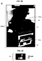
- FIG. 2B is a photograph of an FPI system 10 with components in modular form, according to an embodiment of the invention.
- FPI system 10 comprises an FPI device 100(a).
- the FPI device 100(a) comprises modular components that have been placed in communication with components of an Olympus® BX 41 microscope to transform these components of a conventional microscope into an FPI system 10.
- the FPI device 100(a) includes a programmable two-dimensional LED matrix that has been placed under the specimen stage for illuminations.
- the programmable two-dimensional LED matrix comprises the plurality of light elements 112.
- FIG.2C is a photograph of one of the light elements 112 of the variable illuminator 110(a) the FPI device 100(a) of FIG. 2B .
- This light element 112 is an LED that can provide red, green, and blue illuminations.
- the FPI device 110(a) in FIG. 2B comprises a radiation detector 140(a) in the form of a CCD camera.
- the FPI device 100(a) further comprises an optical element 130(a) in the form of a 2X, 0.08 NA objective lens with an Olympus® BX 41 microscope.
- the field number of the 2X objective lens is 26.5.
- a processor 210 may be in electronic communication with the variable illuminator 110(a) and/or to radiation detector 140(a) through the wires 201.
- a specimen 20 has been provided to the FPI device 100(a) on a slide 202.
- a radiation detector of the FPI device 100 can acquire red, green, and blue low-resolution intensity images during a measurement process.
- the computing device 200 can computationally reconstruct a high-resolution and wide field-of-view color image of the specimen area by iteratively combining low-resolution measurements in Fourier space.
- the processor 210 may computationally reconstruct high-resolution and wide field-of-view red, green, and blue images, and then combine the images to generate a color image.
- the FPI device 110(a) does not require a scanning mechanism for variable illumination.
- Other embodiments may include a scanning mechanism.
- the FPI device 110(b) in FIG. 3 has a mechanism 150 that may be a scanning mechanism.
- the FPI device 110(c) in FIG. 4A has a mechanism 160 that may be a scanning mechanism.
- FIG. 3 is a schematic diagram of a side view of components of an FPI device 100(b), according to an embodiment of the invention.
- FPI device 100(b) comprises a variable illuminator 110(b) comprising a light element 112 that is moved (e.g., scanned) in the x'-direction (direction on the x'-axis) and y'-direction (direction on the y'-axis) to a plurality of N locations.
- Variable illuminator 110(b) also comprises an x '-axis, y '-axis, and z'-axis.
- the light element 112 is moved using a mechanism 150 (e.g., a raster scanner).
- FPI device 100(b) further comprises an optical element 130(b) and a radiation detector 140(b) having a sensing surface 142. Although radiation detector 140(b) is shown at a distance away from optical element 130(b), radiation detector 140(b) may optionally be located at the optical element 130(b).
- the FPI device 100(b) includes an x -axis and a y -axis (not shown) at the in-focus plane 122, and a z -axis orthogonal to the in-focus plane 122.
- the FPI device 100(b) also includes a distance d between the variable illuminator 110(b) and the sample plane 124.
- specimen 20 has been located at a specimen surface 126 for imaging. In other embodiments, specimen 20 may be in other locations for imaging purposes.
- the light element 112 is shown providing illumination at sample time, t i in the measurement process.
- the optical element 130(b) filters light it receives.
- Light filtered by the optical element 130(b) is received at the sensing surface 142 of the radiation detector 140(b).
- the radiation detector 140(b) senses the intensity distribution of the filtered light and captures a low-resolution intensity image of the specimen area.
- the light element 112 includes an X-ray source.
- FIG. 4A is a schematic diagram of a side view of components of an FPI device 100(c), according to embodiments of the invention.
- FPI device 100(c) comprises a variable illuminator 110(c) with a stationary light element 112, an optical element 130(c), a radiation detector 140(c) having a sensing surface 142, and a mechanism 160 (e.g., scanning mechanism).
- a mechanism 160 e.g., scanning mechanism
- the mechanism 160 moves an assembly 170 comprising the optical element 130(c), a radiation detector 140(b) and specimen 20 relative to the stationary light element 112 to provide illumination from a plurality of N incidence angles.
- the mechanism 160 may translate and/or rotate the assembly 170.
- the assembly 170 may mounted on a goniometer sate that would allow the assembly to be rotated as a whole relative to the light element 112.
- the variable illuminator 110(c) also comprises an x '-axis, y '-axis, and z'-axis.
- the FPI device 100(c) includes an x -axis and a y -axis (not shown) at the in-focus plane 122, and a z-axis orthogonal to the in-focus plane 122.
- the FPI device 100(c) also includes a distance d between the variable illuminator 110(c) and the sample plane 124.
- the light element 112 is shown providing illumination at sample time, t i in the measurement process.
- the optical element 130(c) receives and filters light issuing from specimen 20. Light filtered by the optical element 130(c) is received at the sensing surface 142 of the radiation detector 140(c).
- the radiation detector 140(c) senses the intensity distribution of the filtered light and captures a low-resolution intensity image of the area.
- FIG. 4B is a schematic diagram of a side view of components of an FPI device 100(d), according to embodiments of the invention.
- FPI device 100(d) comprises a variable illuminator 110(d) with a light element 112 that is moved by rotating it, an optical element 130(b), and a radiation detector 140(b) having a sensing surface 142.
- a mechanism may also be included to rotate the light element 112.
- specimen 20 has been provided to the FPI device 100(d) for imaging.
- the light element 112 may be a laser.
- the light element 112 is moved by rotating it, which provides illumination at ( ⁇ x i , ⁇ y i ).
- the light element 112 is shown providing illumination at sample time, t i in the measurement process.
- the optical element 130(b) receives and filters light issuing from specimen 20. Light filtered by the optical element 130(b) is received at the sensing surface 142 of the radiation detector 140(b). The radiation detector 140(b) senses the intensity distribution of the filtered light and captures a low-resolution intensity image of the area.
- an FPI method comprises a measurement process, a recovery process, and an optional display process.
- the measurement process the specimen is illuminated from a plurality of incidence angles using the variable illuminator, the optical element filters light issuing from the specimen, and the radiation detector captures a plurality of low resolution intensity images based on the filtered light.
- the recovery process the intensity of each low resolution image obtained by inverse Fourier transformation and filtering of the high resolution reconstruction in Fourier space is replaced by the low-resolution intensity measurement and the corresponding region of the high-resolution reconstruction in Fourier space is iteratively updated.
- the high-resolution image of the specimen may be computationally reconstructed based on a plurality of N low-resolution intensity images.
- images and other output is provided to a display 220.
- FIG. 5A includes a schematic representation of the measurement process (middle) and a recovery process (right-hand side) of an FPI method, according to embodiments of the invention.
- a specimen is illuminated from different incidence angles, and low-resolution intensity images corresponding to these incidence angles are acquired.
- the acquisition of multiple low-resolution intensity images is represented by the arrangement of images in the middle section of FIG. 5A .
- one or more high-resolution, wide field-of-view images are recovered based on the low-resolution intensity measurements from the measurement process.
- the recovery process is represented by the two images at the right-hand side of FIG. 5A , where both high-resolution intensity and phase image data are recovered based on the low-resolution intensity measurements.
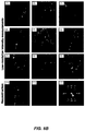
- 5B ( 1 ), 5B ( 2 ), 5B ( 3 ), 5B ( 4 ), 5B ( 5 ), 5B ( 6 ), 5B ( 7 ), 5B ( 8 ), and 5B (9) are nine low-resolution measurements of the 137 measurements acquired by the FPI method introduced in FIG. 5A .
- the corresponding regions associated with the low-resolution images in Fourier space are shown in FIG. 5B (12). During the recovery process, these regions are updated in Fourier space to reconstruct a full FOV high-resolution complex image. Recovered high-resolution intensity and phase images are shown at the right-hand side of FIG. 5A and also shown in FIGS. 5B ( 10 ) and 5B (11).
- the FPI method may alternate between two working domains: the spatial ( x-y ) domain and Fourier ( k x -k y ) domain, where k represents the wavenumber.
- the FPI method may use the concept of oblique incidence, which provides that illuminating the specimen 20 (e.g., a thin specimen) by an oblique plane wave with a wavevector ( k x i , k y i ) is equivalent to shifting the center of the image spectrum by ( k x , k y ) in the Fourier domain.
- oblique incidence the low-resolution image in the Fourier domain is shifted from normal incidence by ( k x , k y ), which corresponds to the incidence angle applied by the variable illuminator.
- the filtering function of the optical element i.e. the coherent optical transfer function
- the FPI method may update in Fourier space circular regions defined by this filtering function of the optical element.
- the FPI method uses this filtering function to omit image data outside this region.
- the image captured is not the specimen image at the specimen profile itself; it is the specimen profile propagated by - z 0 distance at the in-focus plane of the optical element.
- the FPI method may digitally re-focus the specimen 20 propagating the image data by the z 0 distance back to the sample plane 124, without having to mechanically move the specimen in the z-direction.
- These propagating step(s) can be performed by multiplying a phase factor in Fourier space. These steps can extend the imaging depth of focus of the FPI system 10 and correct the chromatic aberration of the optical element.
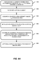
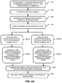
- FIG. 6A is a flowchart of an FPI method performed by an FPI system 10, according to embodiments of the invention.
- the FPI method comprises a measurement process (steps 1100, 1200, and 1300 ), a recovery process (steps 1400 and 1500 ), and an optional display process (step 1600 ).
- subscript "h” refers to high-resolution
- subscript "l” refers to low resolution
- subscript "f” refers to focused position
- subscript "m” refers to measured
- subscript "s” refers to sampled.
- the variable illuminator may provide illumination according to illumination instructions that define the order of the illumination angles.
- the wave vector in x and y directions can be denoted as k xi and k yi .
- the variable illuminator may provide illumination of different wavelengths at different sample times.
- the variable illuminator 110 may provide RGB illumination of three wavelengths ⁇ 1 , ⁇ 2 , and ⁇ 3 corresponding to red, green, blue colors, respectively, for a color imaging embodiment.
- the optical element filters light it receives.
- the optical element can filter light issuing from the specimen 20.
- the optical element may be an objective lens that filters light by accepting light within a range of incidence angles according to its numerical aperture (NA).
- NA numerical aperture
- the optical element may be a low-NA objective lens (e.g., a 2X, 0.08NA objective lens) of a conventional microscope.
- Each low resolution intensity image sampled by the radiation detector is associated with a region in Fourier space.
- the variable illuminator provides illumination from certain incidence angles at step 1100 to generate overlapping areas between neighboring regions in Fourier space.
- the variable illuminator provides illumination to provide an overlapping area between neighboring regions of 2% to 99.5% of the area of one of the regions.
- variable illuminator provides illumination to provide an overlapping area between neighboring regions of 65% to 75% of the area of one of the regions. In one embodiment, the variable illuminator provides illumination to provide an overlapping area between neighboring regions of about 65% of the area of one of the regions.
- a high-resolution image: I h e i ⁇ h is initialized in the spatial domain, and a Fourier transform is applied to the initial value to obtain an initialized Fourier transformed image ⁇ h .
- the Fourier transform of the initial guess can be a broad spectrum in the Fourier domain.
- the high-resolution image of the specimen area is computationally reconstructed by iteratively combining low-resolution intensity measurements in Fourier space using the processor 210 of the FPI system 10.
- the display 230 may receive image data such as the high-resolution image data to I h e i ⁇ h and/or other data from the processor 210, and display the data on the display 230.
- FIG. 6B is a flowchart of sub-steps of step 1500 of FIG. 6A , according to an embodiment of the invention.
- step 1500 comprises step 1510, step 1530, step 1550, step 1560, step 1570, step 1580, and step 1590.
- Step 1500 may optionally comprise steps 1520 and 1540.
- Optional steps 1520 and 1540 may be performed if the specimen 20 is out-of-focus by the amount of z 0 .
- the processor 210 performs low-pass filtering of the high-resolution image I h e i ⁇ h in the Fourier domain to generate a low-resolution image I l e i ⁇ l for a particular plane wave incidence angle ( ⁇ x i , ⁇ y i ) with a wave vector ( k x i , k y i ).
- the Fourier transform of the high-resolution image is ⁇ h and the Fourier transform of the low-resolution image for a particular plane wave incidence angle is ⁇ l .
- the FPI method filters a low-pass region from the spectrum ⁇ h of the high-resolution image I h e i ⁇ h .
- this region is a circular aperture with a radius of NA * k 0 , where k 0 equals 2 ⁇ / ⁇ (the wave number in vacuum), given by the coherent transfer function of an objective lens.
- the location of the region corresponds to the incidence angle.
- the region is centered about a position ( -k x i ,-k y i ) in the Fourier domain of I h e i ⁇ h .
- Step 1520 can be performed by Fourier transforming the low-resolution image I l e i ⁇ l , multiplying by a phase factor in the Fourier domain, and inverse Fourier transforming to obtain I lf e i ⁇ lf .
- step 1520 can be performed by the mathematically equivalent operation of convolving the low-resolution image I l e i ⁇ l with the point-spread-function for the defocus.
- step 1520 can be performed as an optional sub-step of step 1510 by multiplying by multiplying ⁇ t by a phase factor in the Fourier domain before performing the inverse Fourier transform to produce I lf e i ⁇ lf .
- the computed amplitude component I lf of the low-resolution image at the in-focus plane, I lf e i ⁇ lf is replaced with the square root of the low-resolution intensity measurement I lfm measured by the radiation detector of the FPI device. This forms an updated low resolution target: I lfm e i ⁇ lf .
- step 1540 can be performed by taking the Fourier transform of the updated low-resolution image I lfm e i ⁇ lf and multiplying in the Fourier space by a phase factor, and then inverse Fourier transforming it.
- step 1540 can be performed by convolving the updated low-resolution image I lfm e i ⁇ lf with the point-spread-function of the defocus. In another embodiment, step 1540 can be performed as a sub-step of step 1550 by multiplying by a phase factor after performing the Fourier transform onto the updated target image.
- a Fourier transform is applied to the updated target image propagated to the sample plane: I ls e i ⁇ ls , and this data is updated in the corresponding region of high-resolution solution I h e i ⁇ h in the Fourier space corresponding to the corresponding to the incidence wave vector ( k x i , k y i ).
- step 1560 the processor 210 determines whether steps 1510 through 1560 have been completed for all incidence angles. If steps 1510 through 1560 have not been completed for all incidence angles, steps 1510 through 1560 are repeated for the next incidence angle.
- the neighboring regions in Fourier space which are iteratively updated for each incidence angle, overlap each other.
- the FPI system 10 has multiple samplings over the same Fourier space.
- the incidence angles determine the area of the overlapping area.
- the overlapping area between neighboring regions may have an area that is between 2% to 99.5% of the area of one of the neighboring regions.
- the overlapping area between neighboring regions may have an area that is between 65% to 75% of the area of one of the neighboring regions.
- the overlapping area between neighboring regions may have an area that is about 65% of the area of one of the neighboring regions.
- each overlapping region has the same area.
- the processor 210 determines whether the high-resolution solution has converged (step 1570). For example, the processor 210 may determine whether the high-resolution solution may have converged to a self-consistent solution. In one case, the processor 210 compares the previous high-resolution solution of the previous iteration or initial guess to the present high-resolution solution, and if the difference is less than a certain value, the solution may have converged to a self-consistent solution. If processor 210 determines that the solution has not converged, then steps 1510 through 1570 are repeated. In one embodiment, steps 1510 through 1560 are repeated once. In other embodiments, steps 1510 through 1560 are repeated twice or more.
- the processor 210 transforms the converged solution in Fourier space to the spatial domain to recover a high-resolution image I h e i ⁇ h . If the processor 210 determines that the solution has converged at step 1570, then the process may proceed to optional step 1600.
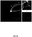
- FIG. 6E is an illustration of steps of the FPI method described with reference to FIGS. 6A and 6B .
- the left-hand-side image in FIG. 6E includes two regions 22(a) and 22(b) with circular low-pass filter shapes in Fourier space of the high-resolution solution, defined by the optical transfer function of a 2X objective lens 0.08NA.
- the dimensions of the regions 22(a) and 22(b) are defined by the optical transfer function of a 2X objective lens 0.08NA based on approximating as circular pupil function with a radius of NA * k 0 , where k 0 equals 2 ⁇ / ⁇ (the wave number in vacuum).
- the region is updated with low-resolution image data having an updated intensity measurement I ls ( k x N , k y N ).
- FIG. 6F is another illustration of steps of the FPI method described with reference to FIGS. 6A and 6B .
- the specimen 20 is at the in-focus plane.
- the schematic drawing includes illustrations 1605, 1606, and 1607.
- Illustration 1605 includes a representative image of an initial Fourier spectrum resulting from step 1400 and the interpolated intensity.
- Illustration 1606 represents the iterative portion of the step 1500, which includes 1510, 1530, 1550 in this case.
- Illustration 1606 includes N iterations.
- Each of the regions 22(d), 22(e), and 22(f) are the circular low-pass filter shapes in Fourier space of the high-resolution solution.
- the dimensions of the regions 22(a) and 22(b) are defined by the optical transfer function of a 2X objective lens 0.08NA based on approximating as circular pupil function with a radius of NA * k 0 , where k 0 equals 2 ⁇ / ⁇ (the wave number in vacuum).
- region 22(f) is updated at step 1550.
- Illustration 1606 includes the recovered phase image and the recovered intensity images.
- the FPI method can include digital refocusing by including optional steps 1520 and 1540.
- digital refocusing may be needed when the specimen 20 is out-of-focus by the amount of z 0 .
- FIG. 6C and 6D are schematic diagrams of components of an FPI device 100(a) with light elements in the form of an LED matrix, according to an embodiment of the invention.
- the specimen 20 is out-of-focus by an amount of- z 0 , and optional steps 1520 and 1540 can be used to digitally refocus.
- the specimen 20 is located at the in-focus position at the in-focus plane 122. In this case, optional steps 1520 and 1540 may not be needed.
- an FPI system 10 with the FPI device 100(a) shown in FIG. 2B was used to perform the FPI method of FIGS. 6A and 6B where the specimen 20 was located at the in-focus plane 122.
- the light elements were in the form of 137 red LEDs as the light sources for oblique illuminations.
- the corresponding maximum NA of the reconstructed image was ⁇ 0.5 in the diagonal direction.
- FIGS. 7A ( 1 ), 7A ( 2 ), 7A ( 3 ), 7A ( 4 ), and 7A (5) are images resulting from performing the FPI method of FIGS. 6A and 6B . These results show improved resolution.
- FIG. 7A (1) is a full field-of-view low-resolution intensity image of the specimen area.
- FIG. 7A (2) is a zoom-in-view of a selected portion of the low resolution image FIG. 7A (1) captured by the radiation detector, with a pixel size of 2.75 ⁇ m (5.5 ⁇ m divided by the magnification factor).
- FIG. 7A (3) is a zoom-in-view of the image in FIG. 7A (2).
- FIGS. 7A ( 4 ) and 7A (5) are computationally reconstructed high-resolution images, where the pixel size is 0.275um.
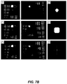
- an FPI system 10 with the FPI device 100(a) shown in FIG. 2B was used to perform the FPI method of FIGS. 6A and 6B where the specimen 20 was located at the in-focus plane 122, with different numbers of LED light sources (i.e. different N number of incidence angles) and their corresponding high-resolution reconstructions with different maximum NAs covered in Fourier space with the reconstruction.
- the specimen 20 was located at the in-focus plane 122, with different numbers of LED light sources (i.e. different N number of incidence angles) and their corresponding high-resolution reconstructions with different maximum NAs covered in Fourier space with the reconstruction.
- FIG. 7B (1) shows resulting high-resolution images from the five frame reconstruction.
- FIG. 7B (2) shows the total spectrum of the five frame reconstruction in Fourier space that spans a maximum synthetic NA of 0.13.
- FIG. 7B (3) shows resulting high-resolution images from the 64 frame reconstruction.
- FIG. 7B (4) shows the spectrum of the 64 frame reconstruction in Fourier space that spans a maximum synthetic NA of 0.3.
- FIG. 7B (5) shows resulting high-resolution images from the 137 frame reconstruction.
- FIG. 7B (6) shows the spectrum of the 137 frame reconstruction in Fourier space that spans a maximum synthetic NA of 0.5.
- 7B ( 2 ), 7B ( 4 ), and 7B (6) represent the spectrum region corresponding to one low-resolution intensity measurement.
- an FPI method with tile imaging divides the captured low-resolution images into a plurality of low-resolution tile images, independently acquires a high-resolution image for each of the tiles, and then combines the high-resolution tile images to generate a full field-of-view high-resolution image.
- the high-resolution tile images may be combined with an image blending process.
- An example of an image blending process is alpha blending which can be found in PCT publication WO1999053469 , entitled “A system and method for performing blending using an over sampled buffer,” filed on April 7, 1999. Since the high-resolution images of the tiles may be acquired independently, this FPI method may allow for parallel computing, which may reduce computation time, and may also reduce memory requirements.
- the light from each light element may be accurately treated as a plane wave for each tile.
- (x c ,y c ) is the central position of each tile of the full field-of-view low-resolution image
- (x i ,y i ) is the position of the i th light element
- h is the distance between the illuminator and the specimen.
- this FPI method can assign a specific aberration-correcting pupil function to each tile in some cases.
- an FPI system 10 comprises a computing device 200 in the form of a personal computer having a processor 210 in the form of an Intel i7 CPU.
- this FPI system 10 performed an FPI method with tile imaging that divides the low-resolution images into tiles of 196 x 196 pixels.
- the processing time for each small image (converting 196 by 196 raw pixels to 1960 by 1960 pixels) is about 3.75 seconds using Matlab.
- the processing time for creating the full field-of-view gigapixel image is about 10 minutes when parallel computing using all 4 cores of the CPU.
- an FPI system 10 can have a processor in the form of a GPU unit, which may reduce processing time by ten-fold.
- the processor 210 may perform steps of the FPI method using another programming language, such as C++, which may reduce processing time.
- C++ another programming language
- An example of this FPI system can be found in Zheng, G., Horstmeyer, R., and Yang, C., "Wide-field, high-resolution Fourier ptychographic microscopy," Nature Photonics (July, 2013 ).
- FIG. 8A is a flowchart of an FPI method with tile imaging, according to an embodiment of the invention.
- This FPI method can be performed by an FPI system 10.
- the FPI system 10 includes a processor 210 with parallel processing capabilities such as, for example, the GPU unit or a processor having multiple cores (i.e. independent central processing units).
- the FPI method comprises a measurement process (steps 1100, 1200, and 1300 ), a recovery process (steps 1350, 2400 (i-M), 2500(i-M), 2590), and an optional display process (step 1600 ).
- the measurements process (steps 1100, 1200, and 1300 ) and display process (step 1600 ) are described with reference to FIG. 6A .
- the processor 210 divides the full field-of-view into a plurality of tiles such as, for example, a two-dimensional matrix of tiles.
- the dimensions of a two-dimensional square matrix of tiles may be in powers of two such as, for example, a 256 by 256 matrix, a 64 x 64 matrix, etc.
- the processor may divide up a full field of view of 5,280 x 4,380 pixels into tiles having an area of 150 x 150 pixels.
- the processor 210 initializes the high-resolution image: I h e i ⁇ h in the spatial domain for each tile (1 to M) independently using parallel computing (step 2400(1)...step 2400(M)).
- a Fourier transform is applied to the initial guess.
- the initial guess may be determined as a random complex matrix (for both intensity and phase).
- the initial guess may be determined as an interpolation of the low-resolution intensity measurement with a random phase.
- Another example of an initial guess is a constant value.
- the Fourier transform of the initial guess can be a broad spectrum in the Fourier domain.
- the processor 210 computationally reconstructs a high-resolution image of each tile (1 to M) independently using parallel computing.
- the processor 210 computationally reconstructs the high-resolution image of each tile by iteratively combining low-resolution intensity images in Fourier space as described with reference to steps 1510, 1530, 1550, 1560, and 1570 shown in FIG. 6B , and described herein. Steps 1520 and 1540 may be included if the specimen is out of focus.
- the processor 210 combines the high-resolution tile images into a full field-of view high-resolution image.
- combining tile images comprises an imaging-blending process such as, for example, alpha blending.
- FIG. 8B are images resulting from preforming an FPI method with tile imaging using image blending, according to an embodiment of the invention.
- the FPI method divided each low-resolution image of 5320-by-4370 pixels into 150-by-150 pixel sized tiles.
- the images are of two neighboring high-resolution tile images.
- the image on the right-hand-side is a high-resolution image that combines the two high-resolution tile images using blending.
- the FPI method generates a blending region that replaces the edge regions of the adjacent tile images in the high-resolution full FOV image.
- the width of the blending region was 50 pixels.
- the blending region may have other widths such as, for example, 6 pixels. With blending, there is no observable boundary in the blending region.
- the image data of the recovered high-resolution two-dimensional image of the specimen area is displayed on the display 230.
- the FPI method with tile imaging may further comprise a procedure that accounts for differences in incident angles between different tiles based on the distance between the tiles and each light element.
- Another limitation of conventional high-NA microscopes is the limited depth-of field.
- the depth-of-field of a conventional microscope with a 20X objective lens with 0.4 NA is about 5 ⁇ m.
- the resolution degrades as the specimen moves away from the in-focus plane 122 due to its limited depth-of-field.
- the operator needs to move the stage to mechanically bring the specimen back into focus.
- a precise mechanical stage is needed in the conventional microscope to bring a specimen into the in-focus position with sub-micron accuracy.
- an FPI system 10 implements an FPI method in which a specimen can be refocused digitally rather than mechanically.
- the FPI method computationally refocuses the out-of-focus specimen 20 during the recovery process.
- the FPI system 10 can expand its depth-of focus beyond the physical limitations of its optical element.
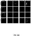
- FIG. 10A are images from a numerical simulation of an FPI system 10 using an FPI method with and without digital refocusing for comparison, according to an embodiment of the invention. These images show that the high-resolution reconstruction resulting from using this FPI method is invariant to the specimen defocusing.
- each row represents a different defocused amount in the z-direction of -150 ⁇ m, -50 ⁇ m, 50 ⁇ m, and 150 ⁇ m.
- Column 1 is the low-resolution image captured.
- Columns 2 and 3 are the recovered high-resolution intensity and phase profiles with digital refocusing.
- Columns 4 and 5 are the recovered high-resolution intensity and phase profiles without digital refocusing.
- FIG. 10B (1) is a schematic diagram of the experimental setup of an FPI device 100(a) performing an FPI method with digital refocusing, according to an embodiment.
- FIGS. 10B (2)-(16) are images of the experimental results from performing the FPI method with digital refocusing according the experimental setup in FIG. 10B (1).
- the specimen was moved to different z positions with defocused distances ranging from-300 ⁇ m to +300 ⁇ m, as shown in the schematic diagram in FIG. 10B (1).
- Low-resolution images (corresponding to 137 different LEDs of an LED matrix) were acquired for all the defocused positions. Representative low resolution images are shown in FIGS. 10B ( 2 ), ( 3 ), ( 4 ), ( 5 ), and ( 6 ).
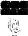
- FIGS. 10C (1)-(7) include more detailed results from the experiment described with respect to FIGS. 10B (1)-10B(16).
- FIG. 10C (7) is a graph of line traces for the smallest features in FIG. 10C ( 4 ), ( 5 ), and ( 6 ).
- the FPI method with digital refocusing can achieve resolution-invariant imaging depth of 0.3 mm.
- FIGS. 10D (1)-(3) are images of experimental results from performing the FPI method with and without digital refocusing for comparison, according to an embodiment of the invention.
- FIGS. 10D ( 2 ) and 10D (3) image reconstructions resulting from using an FPI method of embodiments are shown, with and without digital refocusing (e.g. steps 1520 and 1540 ), for comparison.
- FIG. 10D (2) is a reconstructed high-resolution image with digital refocusing and
- FIG. 10D (3) is a reconstructed high-resolution image without digital refocusing, for comparison.
- Digital refocusing with FPI methods represents another significant improvement over conventional microscopes. Digital refocusing can correct: 1) cases where specimens are not perfectly aligned over the entire field-of-view and 2) for chromatic aberration digitally (assigning different defocused distances for different colors).
- FIGS. 10E ( 1 ), 10E ( 2 ), 10E ( 3 ), 10E ( 4 ), 10E ( 5 ), 10E ( 6 ), 10E ( 7 ), and 10E (8) provide exemplary results from using an FPI system 10 to perform an FPI method with digital refocusing, according to an embodiment of the invention, that corrects for chromatic aberration in a blood smear and in a pathology slide.
- the FPI system 10 includes the FPI device 100(a) of FIG. 2B .
- FIG. 10E (1) is a representative low-resolution image of a blood smear as acquired by the FPI system 10.
- FIG. 10E (2) is a representative low-resolution image of a pathology slide as acquired by the FPI system 10.
- FIG. 10E (1) is a representative low-resolution image of a blood smear as acquired by the FPI system 10.
- FIG. 10E (2) is a representative low-resolution image of a pathology slide as acquired by the FPI system 10.
- FIG. 10E (3) is a high-resolution image of the blood smear as computationally reconstructed with digital refocusing.
- FIG. 10E (4) is a high-resolution image of the pathology slide as computationally reconstructed with digital refocusing.
- FIG. 10E (5) is a high-resolution image of the blood smear as computationally reconstructed without digital refocusing.
- FIG. 10E (6) is a high-resolution image of the pathology slide as computationally reconstructed without digital refocusing.
- FIG. 10E ( 7 ), and 10E (8) are conventional microscope images with a 20X objective lens of the blood smear and pathology slide respectively, for comparison.
- an FPI method may include a digital auto-focusing step that determines the z-position of the specimen 20 and uses this z-position to digitally refocus.
- the FPI method of FIG. 6B may further comprise a step during or before step 1520 that computes the z-position of the specimen 20.
- the FPI system 10 may perform digital autofocusing by using the processor 210 to perform steps 1520 and 1540 in FIG. 6B using the computed z-position of the specimen.
- the FPI method determines an auto-focusing index parameter.
- the auto-focusing index is defined by the following equation: Auto-focusing index : 1 / ⁇ abs I lf ⁇ I lfm
- Eqn. 2 The summation in Eqn. 2 is for all oblique incidence angles.
- the FPI method can digitally refocus to the estimated z-position. In some cases, the high-resolution image solution has been found to converge better when using an accurate z-position.
- FIGS. 10F ( 1 ), 10F ( 2 ), 10F ( 3 ), 10F ( 4 ), 10F ( 5 ), 10F ( 6 ), and 10F (7) include experimental results from using an FPI system 10 to perform an FPI method with digital autofocusing, according to an embodiment of the invention.
- This FPI method computes an auto-focusing index for computing the z-position of the specimen automatically.
- FIGS. 10F ( 1 ), 10F ( 2 ), 10F ( 3 ), 10F ( 4 ), 10F ( 5 ), 10F ( 6 ), and 10F (7) include experimental results from using an FPI system 10 to perform an FPI method with digital autofocusing, according to an embodiment of the invention.
- FIG. 10F (7) is a graph of the computed auto-focus index values for the different z-positions.
- the maximum value of the auto-focusing index indicates the estimated z-position of the specimen.
- the estimated positions based on the maximum calculated auto-focusing indexes are close to the actual positions of the specimen.
- the FPI method can autofocus propagating the image to the estimated position.
- FPI methods do not require phase information as input
- FPI methods of certain embodiments accommodate phase during iterative reconstruction.
- the depth of focus can be extended beyond that of the objective lens using a numerical strategy to compensate for aberrations in the pupil function.
- Examples of such aberration compensation strategies can be found in Gutzler, T., Hillman, T. R., Alexandrov, S. A. and Sampson, D. D., "Coherent aperture-synthesis, wide-field, high-resolution holographic microscopy of biological tissue," Opt. Lett. 35, pp.1136-1138 (2010 ), and Colomb, T. et al., "Automatic procedure for aberration compensation in digital holographic microscopy and applications to specimen shape compensation," Appl. Opt. 45, 851-863 (2006 ).
- the digital correction process digitally introduces a phase map to the coherent optical transfer function to compensate for aberrations at the pupil plane during the iterative image recovery process.
- FIG. 9A is a flowchart of sub-steps of step 1500 of the FPI method of FIG. 6A , according to another embodiment of the invention.
- the FPI method includes digital wavefront correction.
- the FPI method incorporates digital wavefront compensation in the two multiplication steps 1605 and 1645.
- step 1605 models the connection between the actual specimen profile and the captured intensity data (with includes aberrations) through multiplication with a pupil function: e i ⁇ ( k x ,k y ) by the processor 210.
- Step 1645 inverts such a connection to achieve an aberration-free reconstructed image.
- the processor 210 multiplies by a phase factor e i ⁇ ( k x ,k y ) in Fourier domain.
- the processor 210 performs low-pass filtering of the high-resolution image I h e i ⁇ h in the Fourier domain to generate a low-resolution image I l e i ⁇ l for a particular plane wave incidence angle ( ⁇ x i , ⁇ y i ) with a wave vector ( k x i , k y i ).
- the Fourier transform of the high-resolution image is ⁇ h and the Fourier transform of the low-resolution image for a particular plane wave incidence angle is ⁇ l .
- the FPI method filters a low-pass region from the spectrum ⁇ h of the high-resolution image I h e i ⁇ h .
- this region is a circular aperture with a radius of NA * k 0 , where k 0 equals 2 ⁇ / ⁇ (the wave number in vacuum), given by the coherent transfer function of an objective lens.
- the location of the region corresponds to the incidence angle.
- the region is centered about a position ( -k x i ,-k y i ) in the Fourier domain of I h e i ⁇ h .
- the computed amplitude component I lf of the low-resolution image at the in-focus plane, I lf e i ⁇ lf is replaced with the square root of the low-resolution intensity measurement I lfm measured by the radiation detector of the FPI device. This forms an updated low resolution target: I lfm e i ⁇ lf .
- the processor 210 multiplies by an inverse phase factor e -i ⁇ ( k x ,k y ) in Fourier domain.
- a Fourier transform is applied to the updated target image propagated to the sample plane: I ls e i ⁇ ls , and this data is updated in the corresponding region of high-resolution solution I h e i ⁇ h in the Fourier space corresponding to the corresponding to the incidence wave vector ( k x i , k y i ).
- the processor 210 determines whether steps 1605 through 1650 have been completed for all incidence angles. If steps 1605 through 1650 have not been completed for all incidence angles, steps 1605 through 1650 are repeated for the next incidence angle.
- the neighboring regions in Fourier space which are iteratively updated for each incidence angle, overlap each other.
- the FPI system 10 has multiple samplings over the same Fourier space.
- the incidence angles determine the area of the overlapping area.
- the overlapping area between neighboring regions may have an area that is between 2% to 99.5% of the area of one of the neighboring regions.
- the overlapping area between neighboring regions may have an area that is between 65% to 75% of the area of one of the neighboring regions.
- the overlapping area between neighboring regions may have an area that is about 65% of the area of one of the neighboring regions.
- each overlapping region has the same area.
- the processor 210 determines whether the high-resolution solution has converged. For example, the processor 210 may determine whether the high-resolution solution may have converged to a self-consistent solution. In one case, the processor 210 compares the previous high-resolution solution of the previous iteration or initial guess to the present high-resolution solution, and if the difference is less than a certain value, the solution may have converged to a self-consistent solution. If processor 210 determines that the solution has not converged, then steps 1605 through 1670 are repeated. In one embodiment, steps 1605 through 1670 are repeated once. In other embodiments, steps 1605 through 1670 are repeated twice or more.
- the processor 210 transforms the converged solution in Fourier space to the spatial domain to recover a high-resolution image I h e i ⁇ h . If the processor 210 determines that the solution has converged at step 1570, then the process may proceed to optional step 1600.
- FIG. 9B is a schematic diagram of an FPI device 100 implementing an FPI method with digital wavefront correction, according to an embodiment of the invention.
- the digital pupil function is introduced at steps 1605 and 1645 to model the connection between the actual specimen profile and the captured intensity data, which may exhibit aberrations caused by defocus.
- the FPI method with digital wavefront correction can also be used to correct for the spatially varying aberrations of the optical element (e.g., objective lens).
- the FPI method can digitally adjust the 'z' parameter to different values based on a computation of the auto-focusing index from Eqn. 4.
- the FPI method can then reconstruct the corresponding images, and select the sharpest image.
- This approach can also be extended to image a tiled sample.
- the FPI method can digitally adjust the 'z' parameter to achieve acuity for each tiled region of the whole image and combine the in-focus regions to form a fully focused image of the full field of view.
- alternative digital multiplicative phase factors can be included in multiplication steps 1605 and 1645 to correct for a variety of aberrations, as long as the factors correctly model the employed optics.
- the computational cost of the recovery process of the illustrated example of FIG. 6B can be approximated by the computational cost of steps 1510, 1550, and 1570, assuming that the low-resolution images captured by the radiation detector contains n pixels and that N different light elements are used for illuminations.
- step 1510 of the recovery process a two-dimensional fast Fourier transform (FFT) is performed to generate the low-resolution image I l e i ⁇ l and the corresponding computational cost is n 2 ⁇ log(n).
- FFT fast Fourier transform
- another FFT is performed to update the corresponding region of the Fourier space of I hr e i ⁇ hr and the corresponding computational cost is n 2 ⁇ log(n).
- step 1560 the above computation is repeated once for all incidence angles, and thus the computational cost is N ⁇ 2 ⁇ n 2 ⁇ log(n). If step 1570 is repeated once, then the computational cost is 2 ⁇ N ⁇ 2 ⁇ n 2 ⁇ log(n). Other steps in the recovery process are negligible compared to the above value.
- the computational complexity of the FPI method of FIG 6B is 4 ⁇ N ⁇ n 2 ⁇ log(n) where N is the total number of oblique incidences and n is the total number of pixels of the low-resolution image.
- an FPI system 10 capable of color imaging comprises a variable illuminator with an LED having light elements that can provide red, green, and blue illuminations.
- the FPI method combines the high-resolution image results from red, green, and blue LED illumination into each corresponding color channel to form a final high-resolution color image. Three images are generated corresponding to red, green, and blue, which are combined to form a high resolution color image.
- FIG. 11A (1) is a photograph illustrating the fields-of-view of a pathology slide for both 2X and 20X objective lenses of conventional microscopes, for comparison.
- the FOV in the conventional microscope is ⁇ 13.25 mm in diameter and the NA is 0.08, as shown by the images FIGS. 11A ( 2 ) and 11A (3).
- FIGS. 11A ( 4 ) and 11A (5) are color images showing the field-of-view and corresponding maximum NA of an FPI system 10, according to an embodiment of the invention.
- FIG. 11B includes results of using the color imaging FPI system 10, according to an embodiment of the invention.
- the row of figures corresponding to FIGS. 11B (1)-(18) are associated with the reconstructed images for red, green, and blue illumination respectively.
- FIG. 11B (19) is the raw color image.
- FIG. 11B (20) is the computationally reconstructed color image with digital refocusing by the FPI system 10.
- FIG. 11B (21) is an image captured by a 40X objective lens and a color image sensor for comparison.
- FIGS. 11C ( 1 ), 11C ( 2 ), 11C ( 3 ), 11C ( 4 ), 11C ( 5 ) and 11C (6) are color images showing a comparison of image quality between the color imaging FPI system 10 and different objective lenses.
- FIG. 11C ( 1 ), 11C ( 2 ), 11C ( 3 ), 11C ( 4 ), 11C ( 5 ) and 11C (6) are color images showing a comparison of image quality between the color imaging FPI system 10 and different objective lenses
- FIGS. 11C ( 1 ), 11C ( 2 ), 11C ( 3 ), 11C ( 4 ), and 11C (5) are images captured by a 2X, 4X, 10X, 20X, and 40X objective lenses, respectively, for comparison.
- phase profile of a histopathology slide may contain information about the molecular scale organization of tissue and can be used as an intrinsic marker for cancer diagnosis as discussed in Wang, Z., Tangella, K., Balla, A. andffy, G., "Tissue refractive index as marker of disease,” Journal of Biomedical Optics 16, 116017-116017 (2011 ).
- phase information of a sample can also be used to measure the optical path length of cells or organelles to determine the growth pattern of cell cultures or to perform blood screening, as discussed in Lue, N. et al., “Live Cell Refractometry Using Hilbert Phase Microscopy and Confocal Reflectance Microscopy," The Journal of Physical Chemistry A, 113, pp.
- FIG. 11D includes phase and color images from using an FPI method with the color imaging FPI system 10 for both a pathology slide and blood smear, according to an embodiment of the invention.
- FIG. 11D ( 1 ) and 11D (2) are the low-resolution images.
- FIG. 11D ( 3 ) and 11D (4) are the high-resolution intensity images.
- FIG. 11D ( 5 ) and 11D (6) are the high-resolution phase images.
- FIG. 11D ( 1 ) and 11D (2) are the low-resolution images.
- FIG. 11D ( 3 ) and 11D (4) are the high-resolution intensity images.
- FIG. 11D ( 5 ) and 11D (6) are the high-resolution phase images.
- FIG. 11D ( 1 ) and 11D (2) are the low-resolution images.
- FIG. 11D ( 3 ) and 11D (4) are the high-resolution intensity images.
- FIG. 11D ( 5 ) and 11D (6) are the high-resolution phase images
- FIG. 11D ( 7 ) and 11D (8) are the high-resolution color images.
- FIG. 11D ( 9 ) and 11D (10) are images from a conventional microscope with a 20X objective lens for comparison.
- the phase image is generated by taking the phase angle of the complex high-resolution image.
- the FPI systems use FPI methods to reconstruct a high-resolution image with the use of a low NA lens.
- FIG. 5A illustrates results from a numerical simulation of an FPI system using an FPI method, according to an embodiment of the invention.
- FIG. 5A includes two images (left-hand side) that represent the simulated specimen intensity profile I(x,y) and phase profile ⁇ (x,y ). The pixel size of these two input profiles is 275 nm and the wavelength of the simulated incidence is 632 nm.
- the method was performed using an FPI device 100(a) having a plurality of stationary light elements in the form of a two-dimensional array of light elements.
- the specimen was illuminated by plane waves at 137 different incident angles, and filtered by a 2X objective lens (0.08 NA), and then captured by an image sensor with 5.5 ⁇ m pixel size.
- the sample is assumed to be placed at the in-focus position of the objective lens (i.e. at the in-focus plane 122 ).
- the resulting low-resolution images, added with 1% random speckle noise, are shown in the middle part of FIG. 5A . Based on these low-resolution images, a recovery process was used to computationally reconstruct a high-resolution image with a maximum NA of 0.5 in Fourier space.
- the intensity of the low-pass filtered image is replaced by the actual low-resolution measurement and the corresponding Fourier space of the high-resolution reconstruction is updated accordingly.
- Intensity and phase profiles of the reconstructed high-resolution image are shown in the right-hand side of FIG. 5A .
- the high-resolution images of the specimen may be recovered without involving phase measurement in the data acquisition measurement process.
- FIGS. 5B ( 1 ), 5B ( 2 ), 5B ( 3 ), 5B ( 4 ), 5B ( 5 ), 5B ( 6 ), 5B ( 7 ), 5B ( 8 ), 5B ( 9 ), 5B ( 10 ), 5B ( 11 ), and 5B (12) illustrate more results from the numerical simulation of the FPI system using an FPI method, according to the embodiment discussed with respect to FIG. 5A .
- FIGS. 5B ( 1 ), 5B ( 2 ), 5B ( 3 ), 5B ( 4 ), 5B ( 5 ), 5B ( 6 ), 5B ( 7 ), 5B ( 8 ), and 5B (9) are images of 9 low-resolution measurements out of the 137 taken during this simulation.
- FIGS. 5B ( 10 ) and 5B (11) are computationally reconstructed high-resolution intensity and phase images respectively.
- FIG. 5B (12) is the Fourier space of the recovered image. The corresponding regions of the low-resolution images are highlighted.
- the FPI system 10 may have a certain sampling condition to provide a particular enhancement factor.
- the sampling condition may be associated with two questions: 1) given the NA of an objective lens, what is the largest pixel size that can be used for acquiring the low resolution intensity images; 2) given the synthetic NA of the reconstructed image, what is the largest pixel size that can be used for representing the reconstructed intensity image. Since the FPI method of embodiments can recover both intensity and phase information, the answer to question 1 is the same as the sampling condition for coherent optical systems: ⁇ /(2 ⁇ NA obj ). For question 2, the synthetic NA is for the electric field E (with amplitude and phase).
- I E ⁇ E*, where '*' denotes for complex conjugate.
- the passband of the reconstructed intensity image double in the Fourier domain. Therefore, the largest pixel size that can be used for representing the reconstructed intensity image is ⁇ /(4 ⁇ NA obj ) at the sample plane.
- Embodiments of the invention may provide one or more of the following technical advantages. Some examples of these advantages are provided below.
- FPI methods impose object support constraints in the Fourier domain, which provides large FOV and higher signal-to-noise ratio (with focusing elements) without mechanical scanning.
- object support is provided by the confined illumination in the spatial domain.
- the specimen must be mechanically scanned through the desired field-of-view.
- the FPI methods do not require phase measurements of the specimen.
- Conventional interfermometric synthetic aperture microscopes require phase measurements in their detection schemes, as can be described in Rodenburg, J. M. and Bates, R. H. T. "The theory of super-resolution electron microscopy via Wigner-distribution deconvolution," Phil. Trans. R. Soc. Lond. A 339, 521-553 (1992 ), H. M. L. and Rodenburg, J. M., "Movable aperture lensless transmission microscopy, a novel phase retrieval algorithm," Phys. Rev. Lett. 93, 023903 (2004 ), Rodenburg, J. M.
- the FPI systems of certain embodiments may increase the spatial-bandwidth product beyond the physical limitations of its optics while avoiding the drawbacks of previous attempts to do so with conventional devices, in a simple and cost-effective manner.
- These systems use FPI methods to decouple field-of-view from resolution of the optics, which allows these systems to generate a high-resolution image with a low NA lens.
- the throughput of these FPI systems is not limited by the spatial-bandwidth product of their optics.
- an FPI system has been implemented that produces a 1.6 gigapixel system with a maximum NA of 0.5, a field-of-view of 120 mm 2 , and a resolution-invariant imaging depth of 0.3 mm.
- an FPI system can be scaled for a desired throughput by using an objective lens having a particular NA and by using a particular number N of illuminations.
- the throughput of an FPI system may be increased by reducing the NA of the objective lens and/or by increasing the number N of illuminations.
- an FPI system provides two orders of magnitude higher throughput than existing bright-field microscopes without the use of mechanical scanning and/or phase measurements
- components of the FPI system may be in modular form to be readily implemented with components of a conventional microscope or other conventional imaging device. These implementations may have the potential to broadly impact digital pathology, hematology, phytotomy, immunochemistry and forensic photography.
- modular components of an FPI system may include a variable illuminator (e.g., a simple light-emitting diode (LED) matrix) and a processor with instructions for executing the FPI method.
- a variable illuminator e.g., a simple light-emitting diode (LED) matrix
- processor with instructions for executing the FPI method.
- FPI methods do not need mechanical scanning. Unlike conventional synthetic-aperture and scanning-based wide FOV microscopy techniques, mechanical scanning is not required for FPI methods of embodiments. As such, it simplifies the platform design, reduces associated costs and allows for a higher throughput limit.
- an FPI system can be used to generate color images, which is pivotal in pathology and histology applications.
- an FPI system may be capable of color imaging by having a variable illuminator that provides illumination of different colors (e.g., color LED matrix). If digital refocusing is implemented, the computationally reconstructed image can remain free of any chromatic aberrations of the optics.
- FPI methods can computationally refocus the image digitally, rather than mechanically. This aspect is especially useful for cases where specimens are not perfectly aligned over the entire FOV.
- digital refocusing the FPI system can expand the depth of focus beyond the optical limitations of the optical element.
- an FPI method of one embodiment can been used to extend the depth of focus of the objective lens of a conventional microscope from about 80 ⁇ m to about 0.3 mm. This increased depth of focus can provide the additional advantage of providing a large tolerance to microscope slide placement errors, which improves accuracy over conventional systems.
- phase profile of a biological sample contains information about the molecular scale organization of sample and can be used as an intrinsic marker for different applications.
- the ability to perform phase imaging is also useful for digital image processing, such as cell segmentation and cell counting.
- Conventional full-field phase imaging techniques require fairly sophisticated and well-designed optical alignments.
- an FPI method provides an easy and cost-effective solution for researchers and clinicians to incorporate phase imaging functionality into their current microscope systems.
- the FPI method can reconstruct the complex image of the sample.
- the FPI method can generate a phase image by taking the phase angle of the complex image.
- FPI methods can be extended to Terahertz and X-ray imaging applications, where lenses are poor and of very limited numerical aperture.
- an FPI system 10 may be configured for X-ray imaging.
- the Fourier ptychographic X-ray imaging system 10 comprises an FPI device with an X-ray radiation source (e.g., X-ray tube and metal target).
- a Fourier ptychographic X-ray imaging system 10 may include the FPI device 100(c) shown in FIG. 4A , with components configured for use with X-ray radiation.
- the FPI device 110(c) comprises an assembly 170 that may be mounted as a rigid assembly onto a stage (e.g., a goniometer stage) for translating and/or rotating the assembly 170 with respect to a stationary light element 112 directing X-ray radiation to provide X-ray radiation to a specimen 20 from a plurality of N incidence angles.
- the FPI device 100(c) comprises a mechanism 160 for translating and/or rotating the assembly 170 with respect to the light element 112.
- the mechanism 170 may be affixed to a stationary base.
- the FPI device 100(c) also comprises an optical element 130(c) and a radiation detector 140(c). Both of these components are designed for X-ray radiation i.e. an X-ray optical element and an X-ray radiation detector respectively.
- the X-ray optical element may be, for example, a micro zone plate or a grazing incidence mirror. A micro zone plate can project a full-field image to the X-ray radiation detector.
- the X-ray radiation detector may be, for example, an X-ray sensitive CCD.
- the light element 112 may comprise a stationary X-ray radiation source.
- a Fourier ptychographic X-ray imaging system 10 may include the FPI device 100(d) shown in FIG. 4B , with components configured for use with X-ray radiation.
- the FPI device 110(d) comprises a light element 112 directing X-ray radiation to the specimen 20 from a plurality of N incidence angles.
- the FPI device 100(d) rotates the light element 112 relative to the specimen.
- the light element 112 may pivot about one or more axes.
- the FPI device 100(d) also comprises an optical element 130(b) and a radiation detector 140(b).
- the optical element 130(b) and radiation detector 140(b) may be designed for X-ray radiation i.e.
- the light element 112 may comprise an X-ray radiation source.
- the Fourier ptychographic X-ray imaging system 10 may perform the FPI method described with respect to FIG. 6A .
- the FPI method provides illumination to the specimen area from a plurality of N incidence angles by translating and/or rotating the assembly 170 with respect to a stationary light element 112 directing X-ray radiation to provide X-ray radiation to a specimen 20 from a plurality of N incidence angles.
- these Fourier ptychographic X-ray imaging systems 10 provide additional capabilities. For example, these systems may provide larger penetration depths into the specimen. As another example, X-ray imaging may allow for elemental and chemical identification on a scale of 10nm or less.
- FIG. 12 is a block diagram of subsystems that may be present in a FPI system 10, according to embodiments.
- the FPI system 10 includes a processor 210.
- the processor 210 may be a component of the FPI device 100 in some cases.
- the processor 210 may be a component of the radiation detector 140 in some cases.
- FIG. 12 The various components previously described in the Figures may operate using one or more of the subsystems to facilitate the functions described herein. Any of the components in the Figures may use any suitable number of subsystems to facilitate the functions described herein. Examples of such subsystems and/or components are shown in a FIG. 12.
- the subsystems shown in FIG. 12 are interconnected via a system bus 2425. Additional subsystems such as a printer 2430, keyboard 2432, fixed disk 2434 (or other memory comprising computer readable media), display 230, which is coupled to display adapter 2438, and others are shown.
- Peripherals and input/output (I/O) devices which couple to I/O controller 2440, can be connected by any number of means known in the art, such as serial port 2442.
- serial port 2442 or external interface 2444 can be used to connect the computing device 200 to a wide area network such as the Internet, a mouse input device, or a scanner.
- the interconnection via system bus 2425 allows the processor 210 to communicate with each subsystem and to control the execution of instructions from system memory 2446 or the fixed disk 2434, as well as the exchange of information between subsystems.
- the system memory 2446 and/or the fixed disk 2434 may embody the CRM 220 in some cases. Any of these elements may be present in the previously described features.
- an output device such as the printer 2430 or display 230 of the FPI system 10 can output various forms of data.
- the FPI system 10 can output 2D color/monochromatic images (intensity and/or phase), data associated with these images, or other data associated with analyses performed by the FPI system 10.
- Any of the software components or functions described in this application may be implemented as software code to be executed by a processor using any suitable computer language such as, for example, Java, C++ or Perl using, for example, conventional or object-oriented techniques.
- the software code may be stored as a series of instructions, or commands on a CRM, such as a random access memory (RAM), a read only memory (ROM), a magnetic medium such as a hard-drive or a floppy disk, or an optical medium such as a CD-ROM.
- a CRM such as a random access memory (RAM), a read only memory (ROM), a magnetic medium such as a hard-drive or a floppy disk, or an optical medium such as a CD-ROM.
- RAM random access memory
- ROM read only memory
- magnetic medium such as a hard-drive or a floppy disk
- an optical medium such as a CD-ROM.
- Any such CRM may reside on or within a single computational apparatus, and may be present on or within different computational apparatuses within a
Landscapes
- Physics & Mathematics (AREA)
- Engineering & Computer Science (AREA)
- Multimedia (AREA)
- General Physics & Mathematics (AREA)
- Optics & Photonics (AREA)
- Computer Vision & Pattern Recognition (AREA)
- Chemical & Material Sciences (AREA)
- Analytical Chemistry (AREA)
- Biomedical Technology (AREA)
- Health & Medical Sciences (AREA)
- Life Sciences & Earth Sciences (AREA)
- General Health & Medical Sciences (AREA)
- Molecular Biology (AREA)
- Theoretical Computer Science (AREA)
- High Energy & Nuclear Physics (AREA)
- General Engineering & Computer Science (AREA)
- Microscoopes, Condenser (AREA)
- Investigating Or Analysing Materials By Optical Means (AREA)
- Analysing Materials By The Use Of Radiation (AREA)
Applications Claiming Priority (3)
| Application Number | Priority Date | Filing Date | Title |
|---|---|---|---|
| US201261720258P | 2012-10-30 | 2012-10-30 | |
| US201361847472P | 2013-07-17 | 2013-07-17 | |
| PCT/US2013/067068 WO2014070656A1 (en) | 2012-10-30 | 2013-10-28 | Fourier ptychographic imaging systems, devices, and methods |
Publications (3)
| Publication Number | Publication Date |
|---|---|
| EP2915180A1 EP2915180A1 (en) | 2015-09-09 |
| EP2915180A4 EP2915180A4 (en) | 2016-04-27 |
| EP2915180B1 true EP2915180B1 (en) | 2018-12-05 |
Family
ID=50546739
Family Applications (1)
| Application Number | Title | Priority Date | Filing Date |
|---|---|---|---|
| EP13851670.3A Active EP2915180B1 (en) | 2012-10-30 | 2013-10-28 | Fourier ptychographic imaging systems, devices, and methods |
Country Status (9)
| Country | Link |
|---|---|
| US (5) | US10679763B2 (enExample) |
| EP (1) | EP2915180B1 (enExample) |
| JP (1) | JP2015535348A (enExample) |
| CN (2) | CN108761752A (enExample) |
| AU (1) | AU2013338193A1 (enExample) |
| CA (1) | CA2889495A1 (enExample) |
| SG (1) | SG11201503293VA (enExample) |
| TW (1) | TW201428339A (enExample) |
| WO (1) | WO2014070656A1 (enExample) |
Cited By (1)
| Publication number | Priority date | Publication date | Assignee | Title |
|---|---|---|---|---|
| WO2021052992A1 (de) | 2019-09-18 | 2021-03-25 | Siemens Aktiengesellschaft | Aufnahmeeinrichtung zum erzeugen eines hochaufgelösten bildes eines sich durch einen aufnahmebereich bewegenden objekts sowie verfahren |
Families Citing this family (113)
| Publication number | Priority date | Publication date | Assignee | Title |
|---|---|---|---|---|
| US9864184B2 (en) | 2012-10-30 | 2018-01-09 | California Institute Of Technology | Embedded pupil function recovery for fourier ptychographic imaging devices |
| US10652444B2 (en) | 2012-10-30 | 2020-05-12 | California Institute Of Technology | Multiplexed Fourier ptychography imaging systems and methods |
| US10679763B2 (en) | 2012-10-30 | 2020-06-09 | California Institute Of Technology | Fourier ptychographic imaging systems, devices, and methods |
| CN105659143B (zh) | 2013-07-31 | 2019-03-22 | 加州理工学院 | 孔径扫描傅立叶重叠关联成像 |
| WO2015027188A1 (en) | 2013-08-22 | 2015-02-26 | California Institute Of Technoloby | Variable-illumination fourier ptychographic imaging devices, systems, and methods |
| JP6578950B2 (ja) * | 2014-01-07 | 2019-09-25 | ソニー株式会社 | 分析システム、分析プログラム及び分析方法 |
| US9483869B2 (en) * | 2014-01-17 | 2016-11-01 | Intel Corporation | Layered reconstruction for defocus and motion blur |
| US11468557B2 (en) | 2014-03-13 | 2022-10-11 | California Institute Of Technology | Free orientation fourier camera |
| US9817224B2 (en) | 2014-04-30 | 2017-11-14 | University Of Connecticut | Methods and systems for Fourier ptychographic imaging |
| US10162161B2 (en) | 2014-05-13 | 2018-12-25 | California Institute Of Technology | Ptychography imaging systems and methods with convex relaxation |
| WO2015179452A1 (en) * | 2014-05-19 | 2015-11-26 | The Regents Of The University Of California | Fourier ptychographic microscopy with multiplexed illumination |
| DE102014109687B4 (de) | 2014-07-10 | 2020-03-19 | Carl Zeiss Microscopy Gmbh | Positionsbestimmung eines Objekts im Strahlengang einer optischen Vorrichtung |
| DE102014110302B3 (de) * | 2014-07-22 | 2015-09-03 | Carl Zeiss Ag | Verfahren und Vorrichtung zum Abbilden eines Objekts |
| CN104181686B (zh) * | 2014-08-25 | 2016-08-17 | 清华大学深圳研究生院 | 基于fpm的光场显微方法 |
| DE102014112242A1 (de) * | 2014-08-26 | 2016-03-03 | Carl Zeiss Ag | Phasenkontrast-Bildgebung |
| JP2016052116A (ja) * | 2014-08-28 | 2016-04-11 | パナソニックIpマネジメント株式会社 | 画像処理装置、画像処理方法およびコンピュータプログラム |
| DE102014112648A1 (de) * | 2014-08-29 | 2016-03-03 | Carl Zeiss Ag | Bildaufnahmevorrichtung und Verfahren zur Bildaufnahme |
| WO2016061070A1 (en) | 2014-10-14 | 2016-04-21 | Nanotronics Imaging, Inc. | Unique oblique lighting technique using a brightfield darkfield objective and imaging method relating thereto |
| CN105794195B (zh) | 2014-10-27 | 2020-02-07 | 松下知识产权经营株式会社 | 图像形成系统、图像形成方法以及拍摄元件 |
| EP3227741B1 (en) * | 2014-12-04 | 2020-07-08 | California Institute of Technology | Multiplexed fourier ptychography imaging systems and methods |
| WO2016106379A1 (en) * | 2014-12-22 | 2016-06-30 | California Institute Of Technology | Epi-illumination fourier ptychographic imaging for thick samples |
| AU2014280898A1 (en) * | 2014-12-23 | 2016-07-07 | Canon Kabushiki Kaisha | Reconstruction algorithm for Fourier Ptychographic imaging |
| AU2014280894A1 (en) * | 2014-12-23 | 2016-07-07 | Canon Kabushiki Kaisha | Illumination systems and devices for Fourier Ptychographic imaging |
| CA2970063A1 (en) * | 2015-01-21 | 2016-07-28 | California Institute Of Technology | Fourier ptychographic tomography |
| EP3251144A4 (en) | 2015-01-26 | 2018-09-05 | California Institute of Technology | Array level fourier ptychographic imaging |
| JP6528264B2 (ja) * | 2015-01-27 | 2019-06-12 | 国立研究開発法人理化学研究所 | イメージング装置及び方法 |
| US10410398B2 (en) * | 2015-02-20 | 2019-09-10 | Qualcomm Incorporated | Systems and methods for reducing memory bandwidth using low quality tiles |
| MX386279B (es) * | 2015-02-27 | 2025-03-18 | Brigham & Womens Hospital Inc | Sistemas de formacion de imagen y metodos de uso de los mismos. |
| JP2018509622A (ja) | 2015-03-13 | 2018-04-05 | カリフォルニア インスティチュート オブ テクノロジー | フーリエタイコグラフィ手法を用いるインコヒーレント撮像システムにおける収差補正 |
| US9993149B2 (en) | 2015-03-25 | 2018-06-12 | California Institute Of Technology | Fourier ptychographic retinal imaging methods and systems |
| DE102015107517B3 (de) | 2015-05-13 | 2016-06-23 | Carl Zeiss Ag | Vorrichtung und Verfahren zur Bildaufnahme mit erhöhter Schärfentiefe |
| WO2016187591A1 (en) * | 2015-05-21 | 2016-11-24 | California Institute Of Technology | Laser-based fourier ptychographic imaging systems and methods |
| EP3106862B1 (en) * | 2015-06-18 | 2019-01-16 | FEI Company | Method of ptychographic imaging |
| EP3350643B1 (en) * | 2015-09-16 | 2023-04-05 | Technion Research & Development Foundation Limited | Ptychography system |
| US20180348500A1 (en) * | 2015-11-11 | 2018-12-06 | Scopio Labs Ltd. | Scanning microscope with real time response |
| WO2017081542A2 (en) * | 2015-11-11 | 2017-05-18 | Scopio Lab Ltd. | Computational microscopes and methods for generating an image under different illumination conditions |
| US20180373016A1 (en) * | 2015-11-11 | 2018-12-27 | Scopio Labs Ltd. | Microscope having a refractive index matching material |
| JP2017099616A (ja) * | 2015-12-01 | 2017-06-08 | ソニー株式会社 | 手術用制御装置、手術用制御方法、およびプログラム、並びに手術システム |
| US10176567B2 (en) * | 2015-12-21 | 2019-01-08 | Canon Kabushiki Kaisha | Physical registration of images acquired by Fourier Ptychography |
| US10648924B2 (en) * | 2016-01-04 | 2020-05-12 | Kla-Tencor Corp. | Generating high resolution images from low resolution images for semiconductor applications |
| WO2017123128A1 (en) * | 2016-01-14 | 2017-07-20 | Prismatic Sensors Ab | A measurement circuit for an x-ray detector, and a corresponding method and x-ray imaging system |
| WO2017143584A1 (en) | 2016-02-26 | 2017-08-31 | Shenzhen Xpectvision Technology Co., Ltd. | Methods of data output from semiconductor image detector |
| WO2017181044A1 (en) * | 2016-04-15 | 2017-10-19 | The Regents Of The University Of California | Optical phase retrieval systems using color-multiplexed illumination |
| DE102016116311A1 (de) * | 2016-05-02 | 2017-11-02 | Carl Zeiss Microscopy Gmbh | Winkelselektive Beleuchtung |
| US10568507B2 (en) | 2016-06-10 | 2020-02-25 | California Institute Of Technology | Pupil ptychography methods and systems |
| US11092795B2 (en) | 2016-06-10 | 2021-08-17 | California Institute Of Technology | Systems and methods for coded-aperture-based correction of aberration obtained from Fourier ptychography |
| CN106127767B (zh) * | 2016-06-24 | 2019-06-07 | 南京理工大学 | 一种针对傅立叶叠层显微成像技术的位置校正方法 |
| US10048132B2 (en) * | 2016-07-28 | 2018-08-14 | Kla-Tencor Corporation | Simultaneous capturing of overlay signals from multiple targets |
| CN106199941A (zh) * | 2016-08-30 | 2016-12-07 | 浙江大学 | 一种移频光场显微镜以及三维超分辨微观显示方法 |
| CN109923579B (zh) * | 2016-09-28 | 2024-01-26 | 港大科桥有限公司 | 扫描成像中像素分辨率的恢复 |
| US10539783B1 (en) * | 2016-10-17 | 2020-01-21 | National Technology & Engineering Solutions Of Sandia, Llc | Compressive sensing optical design and simulation tool |
| WO2018078447A1 (en) | 2016-10-27 | 2018-05-03 | Scopio Labs Ltd. | Digital microscope which operates as a server |
| US10558029B2 (en) | 2016-10-27 | 2020-02-11 | Scopio Labs Ltd. | System for image reconstruction using a known pattern |
| CN106371201B (zh) * | 2016-11-03 | 2018-11-09 | 清华大学 | 基于计算鬼成像的傅里叶重叠关联成像系统及方法 |
| EP3538941B1 (en) | 2016-11-10 | 2025-04-23 | The Trustees of Columbia University in the City of New York | Rapid high-resolution imaging methods for large samples |
| CN110140348B (zh) * | 2016-12-27 | 2020-12-25 | 富士胶片株式会社 | 摄像装置及摄像模块 |
| CN106767534B (zh) * | 2016-12-30 | 2018-12-11 | 北京理工大学 | 基于fpm的立体显微系统和配套三维面形高分重构方法 |
| DE102017201252A1 (de) * | 2017-01-26 | 2018-07-26 | Universität Ulm | Verfahren und Vorrichtung zur Untersuchung von Zellen |
| CN106875338B (zh) * | 2017-02-16 | 2020-05-08 | 清华大学深圳研究生院 | 一种基于群组稀疏处理的图像超分辨率处理方法 |
| DE102017106984B4 (de) | 2017-03-31 | 2022-02-10 | Carl Zeiss Microscopy Gmbh | Lichtmikroskop und Verfahren zum Betreiben eines Lichtmikroskops mit optimierter Beleuchtungsgeometrie |
| US12099058B2 (en) * | 2017-07-17 | 2024-09-24 | Small Machines | Method for quantitatively analyzing target material and device for quantitatively analyzing target material by using same |
| CN107290846B (zh) * | 2017-08-04 | 2019-06-21 | 南京理工大学 | 基于环状可编程led照明的定量相位显微成像方法 |
| DE102017121291A1 (de) | 2017-09-14 | 2019-03-14 | Carl Zeiss Microscopy Gmbh | Bestimmung von Aberrationen mittels Winkel-variabler Beleuchtung |
| EP3460585B1 (en) * | 2017-09-25 | 2021-07-14 | Imec Vzw | An imaging device for in-line holographic imaging of an object |
| US10754140B2 (en) | 2017-11-03 | 2020-08-25 | California Institute Of Technology | Parallel imaging acquisition and restoration methods and systems |
| US11269172B2 (en) * | 2017-11-24 | 2022-03-08 | Sigtuple Technologies Private Limited | Method and system for reconstructing a field of view |
| CN108362643B (zh) * | 2018-02-10 | 2020-06-16 | 北京工业大学 | 一种双高度照明傅里叶叠层显微成像方法 |
| US10247910B1 (en) | 2018-03-14 | 2019-04-02 | Nanotronics Imaging, Inc. | Systems, devices and methods for automatic microscopic focus |
| US10692184B2 (en) * | 2018-07-05 | 2020-06-23 | SVXR, Inc. | Super-resolution X-ray imaging method and apparatus |
| US20200137380A1 (en) * | 2018-10-31 | 2020-04-30 | Intel Corporation | Multi-plane display image synthesis mechanism |
| US11748863B2 (en) * | 2018-11-30 | 2023-09-05 | Nec Corporation | Image matching apparatus, image matching method, and program |
| WO2020131864A1 (en) | 2018-12-18 | 2020-06-25 | Pathware Inc. | Computational microscopy based-system and method for automated imaging and analysis of pathology specimens |
| CN110286482A (zh) * | 2019-05-24 | 2019-09-27 | 北京理工大学 | 一种分组式傅里叶叠层显微重建方法 |
| US11523046B2 (en) * | 2019-06-03 | 2022-12-06 | Molecular Devices, Llc | System and method to correct for variation of in-focus plane across a field of view of a microscope objective |
| CN112051239B (zh) * | 2019-06-05 | 2024-04-12 | 中国科学院上海光学精密机械研究所 | 基于动态散射系统的在探测面积受限情况下的成像方法 |
| JP7322549B2 (ja) * | 2019-06-28 | 2023-08-08 | セイコーエプソン株式会社 | 画像処理方法および画像処理装置 |
| CN110378981B (zh) * | 2019-07-19 | 2022-11-15 | 中国科学院长春光学精密机械与物理研究所 | 基于神经网络的傅里叶叠层显微镜光瞳恢复方法 |
| US11854281B2 (en) * | 2019-08-16 | 2023-12-26 | The Research Foundation For The State University Of New York | System, method, and computer-accessible medium for processing brain images and extracting neuronal structures |
| KR102278782B1 (ko) * | 2019-09-16 | 2021-07-20 | 주식회사 스몰머신즈 | 능동 가변 스펙클 조명 대면적 고해상도 영상 기기 및 이를 이용한 이미징 방법 |
| CN114342036B (zh) * | 2019-09-20 | 2024-08-23 | 株式会社日立高新技术 | 带电粒子显微镜装置及其视野调整方法 |
| CN110942423B (zh) * | 2019-10-08 | 2023-04-28 | 杭州电子科技大学 | 一种基于傅里叶叠层成像的远场超分辨率重建方法 |
| CN112666697B (zh) * | 2019-10-15 | 2022-06-10 | 南京理工大学 | 基于彩色复用照明的单帧差分相衬定量相位成像方法 |
| US20220413276A1 (en) * | 2019-12-02 | 2022-12-29 | Lam Research Corporation | Reflective fourier ptychography imaging of large surfaces |
| US11640657B2 (en) * | 2020-02-03 | 2023-05-02 | Arizona Board Of Regents On Behalf Of The University Of Arizona | System and method for measuring distorted illumination patterns and correcting image artifacts in structured illumination imaging |
| KR102315010B1 (ko) * | 2020-02-19 | 2021-10-21 | 한국표준과학연구원 | 파라볼릭 미러를 이용한 반사형 fpm |
| KR102432435B1 (ko) * | 2020-05-04 | 2022-08-17 | 주식회사 스몰머신즈 | 발광소자 어레이를 이용한 영상 획득 방법 및 장치 |
| KR20230027012A (ko) * | 2020-05-12 | 2023-02-27 | 피엑스이 컴퓨테이셔널 이미징 엘티디 | 디지털 광학 수차 보정 및 스펙트럼 이미징을 위한 시스템 및 방법 |
| US11689821B2 (en) | 2020-08-07 | 2023-06-27 | The Government Of The United States Of America, As Represented By The Secretary Of The Navy | Incoherent Fourier ptychographic super-resolution imaging system with priors |
| CN112255776B (zh) * | 2020-11-10 | 2022-08-02 | 四川欧瑞特光电科技有限公司 | 一种点光源扫描照明方法及检测装置 |
| EP4013048A1 (en) * | 2020-12-08 | 2022-06-15 | Koninklijke Philips N.V. | Object visualization |
| TWI831078B (zh) | 2020-12-11 | 2024-02-01 | 國立中央大學 | 應用影像還原的光學系統及光學影像處理方法 |
| CN112946373B (zh) * | 2021-02-01 | 2024-02-09 | 北京邮电大学 | 一种基于紧缩场系统的无相位测量方法及装置 |
| WO2022183078A1 (en) * | 2021-02-25 | 2022-09-01 | California Institute Of Technology | Computational refocusing-assisted deep learning |
| ES3020085T3 (en) * | 2021-05-17 | 2025-05-21 | Ceram Data Solutions Gmbh | High-speed reading by combining transmissive wide angle view with reflective focus view |
| CN113341553B (zh) * | 2021-05-27 | 2022-09-20 | 杭州电子科技大学 | 一种傅里叶叠层显微彩色成像方法 |
| KR102578264B1 (ko) * | 2021-08-11 | 2023-09-20 | 재단법인 아산사회복지재단 | 호흡기도 섬모세포 운동성 측정 방법 및 장치 |
| US12504363B2 (en) | 2021-08-17 | 2025-12-23 | California Institute Of Technology | Three-dimensional contoured scanning photoacoustic imaging and virtual staining |
| CN113671682B (zh) * | 2021-08-23 | 2023-05-23 | 北京理工大学重庆创新中心 | 一种基于傅里叶叠层显微成像的频域光源位置精确校正方法 |
| US12461989B2 (en) * | 2021-11-19 | 2025-11-04 | Minitab, Llc | Correcting low-resolution measurements |
| CN114066735B (zh) * | 2021-11-30 | 2024-10-15 | 重庆邮电大学 | 基于最小一乘的稀疏采样傅里叶叠层成像人工神经网络重建方法 |
| CN114170344B (zh) * | 2021-12-31 | 2025-04-18 | 中国联合网络通信集团有限公司 | 基于关联成像的图像重建方法及装置 |
| US12455236B2 (en) | 2022-02-15 | 2025-10-28 | Rensselaer Polytechnic Institute | Polarimetric coherent diffraction imaging |
| TWI787134B (zh) * | 2022-05-26 | 2022-12-11 | 國立臺灣大學 | 一種用於快速雜訊抑制對比度增強的資料處理方法及包含其的影像採集和處理系統 |
| WO2024013161A1 (en) * | 2022-07-15 | 2024-01-18 | Asml Netherlands B.V. | Obtaining high resolution information from low resolution images |
| US20240153034A1 (en) * | 2022-11-03 | 2024-05-09 | Electronics And Telecommunications Research Institute | Apparatus and method for expressing microscopy data |
| US12352946B1 (en) * | 2022-12-15 | 2025-07-08 | United States Of America As Represented By The Administrator Of Nasa | Fourier ptychographic microscope systems and methods |
| EP4619811A1 (en) * | 2022-12-23 | 2025-09-24 | Siemens Healthcare Diagnostics, Inc. | Methods and apparatus for fourier ptychography reconstruction processing |
| KR20240108945A (ko) | 2023-01-03 | 2024-07-10 | 삼성전자주식회사 | 기판 검사 장치 및 기판 검사 방법 |
| CN116430571B (zh) * | 2023-03-30 | 2025-07-22 | 南京理工大学 | 多模态超分辨定量相位显微成像方法 |
| US20260063474A1 (en) * | 2023-08-17 | 2026-03-05 | California Institute Of Technology | Volumetric metaoptics for multi-dimensional wavefront sensing |
| KR102924417B1 (ko) * | 2023-12-28 | 2026-02-05 | 연세대학교 산학협력단 | 편광 조명을 이용한 단일 영상 기반 퓨리에 타이코그래피 이미징 장치 및 방법 |
| DE102024202667A1 (de) * | 2024-03-21 | 2025-09-25 | Carl Zeiss Smt Gmbh | Verfahren zum Erfassen von optischen Eigenschaften eines Mikroskops, Verfahren zur Wiederherstellung der Abbildungsqualität eines Mikroskops sowie zur Durchführung des Verfahrens geeignetes Mikroskop |
| CN119424044B (zh) * | 2024-12-05 | 2025-07-29 | 无锡蕾明视康科技有限公司 | 一种基于空间滤波的带晶体眼人工晶状体及其制备方法 |
Family Cites Families (199)
| Publication number | Priority date | Publication date | Assignee | Title |
|---|---|---|---|---|
| US4873653A (en) | 1986-04-09 | 1989-10-10 | Carl-Zeiss-Stiftung | Microscope system for providing three-dimensional resolution |
| US4917494A (en) | 1987-07-28 | 1990-04-17 | Amherst Process Instruments, Inc. | Beam forming apparatus for aerodynamic particle sizing system |
| US5719405A (en) * | 1992-09-01 | 1998-02-17 | Nikon Corporation | Particle inspecting apparatus and method using fourier transform |
| US5475527A (en) | 1994-09-26 | 1995-12-12 | The Regents Of The University Of California | Fourier plane image amplifier |
| US5774222A (en) * | 1994-10-07 | 1998-06-30 | Hitachi, Ltd. | Manufacturing method of semiconductor substrative and method and apparatus for inspecting defects of patterns on an object to be inspected |
| WO1996028751A1 (en) * | 1995-03-16 | 1996-09-19 | Philips Electronics N.V. | Method for particle wave reconstruction in a particle-optical apparatus |
| KR19980075050A (ko) | 1997-03-28 | 1998-11-05 | 윤종용 | 주사 전자 현미경의 가변어퍼쳐 |
| US6144365A (en) | 1998-04-15 | 2000-11-07 | S3 Incorporated | System and method for performing blending using an over sampling buffer |
| US6154196A (en) | 1998-06-08 | 2000-11-28 | Wacom Co., Ltd. | Coordinate input device convertible between right-handed and left-handed modes |
| US6320648B1 (en) | 1998-10-12 | 2001-11-20 | Steven R. J. Brueck | Method and apparatus for improving pattern fidelity in diffraction-limited imaging |
| DE19949029C2 (de) | 1999-10-11 | 2002-11-21 | Innovatis Gmbh | Verfahren und Vorrichtung zur Charakterisierung einer Kulturflüssigkeit |
| US6320174B1 (en) | 1999-11-16 | 2001-11-20 | Ikonisys Inc. | Composing microscope |
| US20010055062A1 (en) | 2000-04-20 | 2001-12-27 | Keiji Shioda | Operation microscope |
| JP3710704B2 (ja) * | 2000-11-28 | 2005-10-26 | 日本電信電話株式会社 | 画像パターンの回転角度検出誤差低減方法及びこの方法の実行プログラムを記録した記録媒体 |
| US6856457B2 (en) | 2001-03-27 | 2005-02-15 | Prairie Technologies, Inc. | Single and multi-aperture, translationally-coupled confocal microscope |
| DE10128476C2 (de) | 2001-06-12 | 2003-06-12 | Siemens Dematic Ag | Optische Sensorvorrichtung zur visuellen Erfassung von Substraten |
| GB0115714D0 (en) * | 2001-06-27 | 2001-08-22 | Imperial College | Structure determination of macromolecules |
| US6747781B2 (en) | 2001-06-25 | 2004-06-08 | Silicon Light Machines, Inc. | Method, apparatus, and diffuser for reducing laser speckle |
| US6741730B2 (en) | 2001-08-10 | 2004-05-25 | Visiongate, Inc. | Method and apparatus for three-dimensional imaging in the fourier domain |
| US6870165B2 (en) | 2001-10-19 | 2005-03-22 | Biocal Technology, Inc. | Multi-color multiplexed analysis in a bio-separation system |
| EP2275775B1 (en) | 2002-01-16 | 2015-09-23 | Faro Technologies, Inc. | Laser-based coordinate measuring device and laser-based method for measuring coordinates |
| US6759949B2 (en) | 2002-05-23 | 2004-07-06 | Visteon Global Technologies, Inc. | Image enhancement in far infrared camera |
| US7130115B2 (en) | 2002-09-23 | 2006-10-31 | Dhetrix, Inc. | Multi-mode scanning imaging system |
| JP4360817B2 (ja) | 2002-10-18 | 2009-11-11 | 株式会社日立メディコ | 放射線断層撮影装置 |
| WO2004090581A2 (en) | 2003-03-31 | 2004-10-21 | Cdm Optics, Inc. | Systems and methods for minimizing aberrating effects in imaging systems |
| JP4377171B2 (ja) | 2003-07-15 | 2009-12-02 | Tdk株式会社 | 空間光変調器 |
| US7738095B2 (en) | 2003-07-18 | 2010-06-15 | Chemimage Corporation | Method and apparatus for compact spectrometer for detecting hazardous agents |
| US7823783B2 (en) | 2003-10-24 | 2010-11-02 | Cognex Technology And Investment Corporation | Light pipe illumination system and method |
| US8271251B2 (en) * | 2004-02-09 | 2012-09-18 | Wisconsin Alumni Research Foundation | Automated imaging system for single molecules |
| US7173256B2 (en) | 2004-03-26 | 2007-02-06 | Fox John S | Fluorescent image calibration step wedge, and use thereof in illumination for fluorescent imaging and automatic exposure |
| DE102004017232A1 (de) | 2004-04-05 | 2005-10-20 | Bosch Gmbh Robert | Interferometrische Messvorrichtung |
| JP4771944B2 (ja) * | 2004-06-16 | 2011-09-14 | 株式会社日立メディコ | 放射線断層像撮像装置 |
| US7436503B1 (en) | 2004-08-03 | 2008-10-14 | Kla-Tencor Technologies Corp. | Dark field inspection apparatus and methods |
| CA2576528A1 (en) | 2004-08-09 | 2006-02-16 | Classifeye Ltd. | Non-contact optical means and method for 3d fingerprint recognition |
| US7545571B2 (en) | 2004-09-08 | 2009-06-09 | Concurrent Technologies Corporation | Wearable display system |
| EP1640706A1 (en) | 2004-09-22 | 2006-03-29 | Eldim Sa | Wavelength and incidence angle resolved ellipsometer or reflectometer |
| US20060173313A1 (en) | 2005-01-27 | 2006-08-03 | Siemens Medical Solutions Usa, Inc. | Coherence factor adaptive ultrasound imaging |
| US7653232B2 (en) * | 2005-01-28 | 2010-01-26 | University Of Massachusetts | Phase based digital imaging |
| US8654201B2 (en) | 2005-02-23 | 2014-02-18 | Hewlett-Packard Development Company, L.P. | Method for deblurring an image |
| EP1866616B1 (en) | 2005-04-05 | 2013-01-16 | The Board Of Trustees Of The Leland Stanford Junior University | Optical image processing using minimum phase functions |
| EP2703871A3 (en) | 2005-05-25 | 2014-09-03 | Massachusetts Institute Of Technology | Multifocal scanning microscopy systems and methods |
| CN101203790A (zh) | 2005-06-03 | 2008-06-18 | 博奥生物有限公司 | 一种微阵列芯片激光扫描仪光学系统 |
| WO2006133509A1 (en) | 2005-06-16 | 2006-12-21 | Swinburne University Of Technology | Imaging system |
| JP2007071803A (ja) | 2005-09-09 | 2007-03-22 | Hitachi High-Technologies Corp | 欠陥観察方法及びその装置 |
| JP4696890B2 (ja) | 2005-12-12 | 2011-06-08 | 富士ゼロックス株式会社 | ホログラム記録方法及びホログラム記録装置 |
| JP4727517B2 (ja) | 2006-01-11 | 2011-07-20 | 富士フイルム株式会社 | 光源装置および光断層画像化装置 |
| US20070171430A1 (en) | 2006-01-20 | 2007-07-26 | The General Hospital Corporation | Systems and methods for providing mirror tunnel micropscopy |
| JP4822925B2 (ja) | 2006-04-28 | 2011-11-24 | 日本電子株式会社 | 透過型電子顕微鏡 |
| US7460248B2 (en) | 2006-05-15 | 2008-12-02 | Carestream Health, Inc. | Tissue imaging system |
| US8980179B2 (en) | 2006-05-17 | 2015-03-17 | University Of Maryland, Baltimore County | Angular-dependent metal-enhanced fluorescence |
| JP5174810B2 (ja) | 2006-06-16 | 2013-04-03 | カール・ツァイス・エスエムティー・ゲーエムベーハー | マイクロリソグラフィ投影露光装置の投影対物器械 |
| BRPI0715216A2 (pt) * | 2006-08-03 | 2013-06-18 | The Regents Of The University Of California | mÉtodo para reconstruir uma representaÇço da imagem de um objeto a partir de suas projeÇÕes e para tratar imagens tomogrÁficas, e, produto de programa de computador |
| US7838302B2 (en) | 2006-08-07 | 2010-11-23 | President And Fellows Of Harvard College | Sub-diffraction limit image resolution and other imaging techniques |
| CN100385275C (zh) | 2006-09-29 | 2008-04-30 | 李志扬 | 主动光学位相共轭方法及装置 |
| JP4690379B2 (ja) | 2006-12-05 | 2011-06-01 | 韓國電子通信研究院 | 偏光板と高速フーリエ変換を用いたナノ線感知用光学顕微鏡システム |
| US20080192343A1 (en) | 2007-02-09 | 2008-08-14 | Sony Corporation | Three-dimensional image display apparatus |
| JP2010530075A (ja) | 2007-03-20 | 2010-09-02 | クロマ テクノロジー コーポレイション | 光源 |
| US8313031B2 (en) | 2007-03-30 | 2012-11-20 | Symbol Technologies, Inc. | Adaptive aperture for an imaging scanner |
| WO2008124832A1 (en) | 2007-04-10 | 2008-10-16 | University Of Rochester | Structured illumination for imaging of stationary and non-stationary, fluorescent and non-flourescent objects |
| US8624968B1 (en) | 2007-04-25 | 2014-01-07 | Stc.Unm | Lens-less digital microscope |
| CN101743519B (zh) | 2007-05-16 | 2013-04-24 | 视瑞尔技术公司 | 全息显示装置 |
| WO2008152801A1 (ja) | 2007-06-13 | 2008-12-18 | Nikon Corporation | 検査装置、検査方法およびプログラム |
| US7759620B2 (en) | 2007-07-03 | 2010-07-20 | Micronic Laser Systems Ab | Fourier plane analysis and refinement of SLM calibration |
| WO2009009081A2 (en) | 2007-07-10 | 2009-01-15 | Massachusetts Institute Of Technology | Tomographic phase microscopy |
| JP5136778B2 (ja) | 2007-08-20 | 2013-02-06 | セイコーエプソン株式会社 | ラインヘッド及びそれを用いた画像形成装置 |
| US7929142B2 (en) | 2007-09-25 | 2011-04-19 | Microsoft Corporation | Photodiode-based bi-directional reflectance distribution function (BRDF) measurement |
| JP2011504613A (ja) | 2007-11-23 | 2011-02-10 | コーニンクレッカ フィリップス エレクトロニクス エヌ ヴィ | マルチモーダルスポットジェネレータとマルチモーダル・マルチスポット・スキャンマイクロスコープ |
| US9239455B2 (en) * | 2007-12-31 | 2016-01-19 | Stc.Unm | Structural illumination and evanescent coupling for the extension of imaging interferometric microscopy |
| US8115992B2 (en) * | 2007-12-31 | 2012-02-14 | Stc.Unm | Structural illumination and evanescent coupling for the extension of imaging interferometric microscopy |
| CN101408623B (zh) | 2008-01-23 | 2011-01-19 | 北京航空航天大学 | 宽带综合孔径上变频成像系统 |
| ES2338197B2 (es) | 2008-05-23 | 2012-10-15 | Universidad De Cadiz | Sistema automatizado y procedimiento para la obtencion de imagenes totalmente focalizadas con microscopios de elevada magnificacion. |
| JP2010012222A (ja) | 2008-06-06 | 2010-01-21 | Olympus Medical Systems Corp | 医療装置 |
| US8184279B2 (en) | 2008-06-16 | 2012-05-22 | The Regents Of The University Of Colorado, A Body Corporate | Fourier domain sensing |
| US7787588B1 (en) * | 2008-07-21 | 2010-08-31 | Xradia, Inc. | System and method for quantitative reconstruction of Zernike phase-contrast images |
| CN102159934A (zh) | 2008-09-26 | 2011-08-17 | 株式会社堀场制作所 | 颗粒物性测量装置 |
| US8019136B2 (en) | 2008-12-03 | 2011-09-13 | Academia Sinica | Optical sectioning microscopy |
| GB0822149D0 (en) | 2008-12-04 | 2009-01-14 | Univ Sheffield | Provision of image data |
| JP5746045B2 (ja) | 2008-12-22 | 2015-07-08 | スリーエム イノベイティブ プロパティズ カンパニー | 複数の複屈折層を有する内部パターン形成多層光学フィルム |
| WO2010090849A1 (en) | 2009-01-21 | 2010-08-12 | California Institute Of Technology | Quantitative differential interference contrast (dic) devices for computed depth sectioning |
| US8836948B2 (en) | 2009-01-29 | 2014-09-16 | The Regents Of The University Of California | High resolution structured illumination microscopy |
| CN101872033B (zh) | 2009-04-24 | 2014-04-30 | 鸿富锦精密工业(深圳)有限公司 | 遮光片阵列、遮光片阵列制造方法及镜头模组阵列 |
| US8551425B2 (en) | 2009-05-20 | 2013-10-08 | California Institute Of Technology | Method for cancer detection, diagnosis and prognosis |
| US20160156880A1 (en) | 2009-06-03 | 2016-06-02 | Flir Systems, Inc. | Durable compact multisensor observation devices |
| US8559014B2 (en) * | 2009-09-25 | 2013-10-15 | Hwan J. Jeong | High-resolution, common-path interferometric imaging systems and methods |
| EP3136079B1 (en) | 2009-10-20 | 2020-02-12 | The Regents of The University of California | Incoherent lensfree cell holography and microscopy on a chip |
| US20140152801A1 (en) * | 2009-10-28 | 2014-06-05 | Alentic Microscience Inc. | Detecting and Using Light Representative of a Sample |
| US8497934B2 (en) | 2009-11-25 | 2013-07-30 | Massachusetts Institute Of Technology | Actively addressable aperture light field camera |
| DE102009047361B4 (de) | 2009-12-01 | 2013-02-07 | Fraunhofer-Gesellschaft zur Förderung der angewandten Forschung e.V. | Vorrichtung zur optischen Abbildung |
| CN101726366B (zh) | 2009-12-02 | 2011-11-23 | 山东师范大学 | 一种基于多针孔板的波前测量方法和装置 |
| WO2011093043A1 (ja) * | 2010-01-27 | 2011-08-04 | 国立大学法人北海道大学 | 回折顕微法 |
| EP2534667A2 (en) | 2010-02-10 | 2012-12-19 | Mochii, Inc. (d/b/a Voxa) | Aberration-correcting dark-field electron microscopy |
| JP5538936B2 (ja) | 2010-02-10 | 2014-07-02 | キヤノン株式会社 | 解析方法、プログラム、記憶媒体、x線位相イメージング装置 |
| CN102947864B (zh) | 2010-06-21 | 2015-08-12 | 皇家飞利浦电子股份有限公司 | 用于执行低剂量ct成像的方法和系统 |
| US9129371B2 (en) | 2010-06-25 | 2015-09-08 | Cireca Theranostics, Llc | Method for analyzing biological specimens by spectral imaging |
| GB2481589B (en) | 2010-06-28 | 2014-06-11 | Phase Focus Ltd | Calibration of a probe in ptychography |
| JP5878121B2 (ja) | 2010-07-13 | 2016-03-08 | 株式会社テレシステムズ | X線断層像撮影装置 |
| US8599367B2 (en) | 2010-08-04 | 2013-12-03 | Alliant Techsystems Inc. | Apparatus and methods for obtaining multi-dimensional spatial and spectral data with LIDAR detection |
| US20130170024A1 (en) | 2010-09-14 | 2013-07-04 | Applied Precision, Inc. | Oblique-illumination systems and methods |
| US9185357B2 (en) | 2010-09-17 | 2015-11-10 | Lltech Management | Optical tissue sectioning using full field optical coherence tomography |
| CN101957183B (zh) | 2010-09-26 | 2012-03-21 | 深圳大学 | 一种结构光投影的高速三维测量系统 |
| US9569664B2 (en) | 2010-10-26 | 2017-02-14 | California Institute Of Technology | Methods for rapid distinction between debris and growing cells |
| US9426429B2 (en) | 2010-10-26 | 2016-08-23 | California Institute Of Technology | Scanning projective lensless microscope system |
| GB201020516D0 (en) | 2010-12-03 | 2011-01-19 | Univ Sheffield | Improvements in providing image data |
| WO2012088351A2 (en) | 2010-12-21 | 2012-06-28 | The Regents Of The University Of California | Compact wide-field fluorescent imaging on a mobile device |
| US9411144B2 (en) | 2011-01-12 | 2016-08-09 | Ge Healthcare Bio-Sciences Corp. | Systems for fluorescence illumination using superimposed polarization states |
| WO2012102887A2 (en) | 2011-01-24 | 2012-08-02 | The Board Of Trustees Of The University Of Illinois | Computational adaptive optics for interferometric synthetic aperture microscopy and other interferometric imaging |
| CN102652680A (zh) * | 2011-03-01 | 2012-09-05 | 贺宁 | 基于非均匀傅里叶变换的超声层析成像方法 |
| WO2012119094A2 (en) | 2011-03-03 | 2012-09-07 | California Institute Of Technology | Light guided pixel |
| US8866063B2 (en) | 2011-03-31 | 2014-10-21 | The Regents Of The University Of California | Lens-free wide-field super-resolution imaging device |
| US8841591B2 (en) | 2011-04-04 | 2014-09-23 | The Board Of Trustees Of The Leland Stanford Junior University | Grating-enhanced optical imaging |
| GB201107053D0 (en) | 2011-04-27 | 2011-06-08 | Univ Sheffield | Improvements in providing image data |
| US8761533B2 (en) | 2011-05-05 | 2014-06-24 | Mitsubishi Electric Research Laboratories, Inc. | Method for performing image processing applications using quadratic programming |
| US20140160236A1 (en) * | 2011-07-29 | 2014-06-12 | The Regents Of The University Of California | Lensfree holographic microscopy using wetting films |
| WO2013018024A1 (en) | 2011-07-29 | 2013-02-07 | Ecole Polytechnique Federale De Lausanne (Epfl) | Apparatus and method for quantitative phase tomography through linear scanning with coherent and non-coherent detection |
| IN2014CN01634A (enExample) | 2011-09-06 | 2015-05-08 | Koninkl Philips Nv | |
| US20190097524A1 (en) | 2011-09-13 | 2019-03-28 | Fsp Technology Inc. | Circuit having snubber circuit in power supply device |
| CN103842799B (zh) | 2011-09-30 | 2017-09-08 | 通用电气公司 | 用于样本阵列的自参考检测与成像的系统和方法 |
| US20130093871A1 (en) | 2011-10-18 | 2013-04-18 | Andreas G. Nowatzyk | Omnidirectional super-resolution microscopy |
| US9599805B2 (en) | 2011-10-19 | 2017-03-21 | National Synchrotron Radiation Research Center | Optical imaging system using structured illumination |
| US9324133B2 (en) | 2012-01-04 | 2016-04-26 | Sharp Laboratories Of America, Inc. | Image content enhancement using a dictionary technique |
| GB201201140D0 (en) | 2012-01-24 | 2012-03-07 | Phase Focus Ltd | Method and apparatus for determining object characteristics |
| WO2013116316A1 (en) | 2012-01-30 | 2013-08-08 | Scanadu Incorporated | Hyperspectral imaging systems, units, and methods |
| CN102629371A (zh) * | 2012-02-22 | 2012-08-08 | 中国科学院光电技术研究所 | 基于实时盲图像复原技术的视频像质改善系统 |
| CN102608597B (zh) | 2012-03-19 | 2014-07-23 | 西安电子科技大学 | 基于非完全数据解卷积的实孔径前视成像方法 |
| US9081175B2 (en) | 2012-03-23 | 2015-07-14 | Lumos Technology Co., Ltd. | Fluorescence observation device, domed base and fluorescence microscope provided with multiple light sources having different illumination angles |
| CN103377746B (zh) | 2012-04-14 | 2015-12-02 | 中国科学技术大学 | 实现显微镜系统超分辨成像的方法 |
| US9715098B2 (en) | 2012-05-31 | 2017-07-25 | The Board Of Trustees Of The University Of Illinois | Sparse deconvolution spatial light microscopy in two and three dimensions |
| EP2690648B1 (en) | 2012-07-26 | 2014-10-15 | Fei Company | Method of preparing and imaging a lamella in a particle-optical apparatus |
| WO2014018584A1 (en) | 2012-07-24 | 2014-01-30 | Trustees Of Boston University | Partitioned aperture wavefront imaging method and system |
| US9552658B2 (en) | 2012-07-26 | 2017-01-24 | William Marsh Rice University | Methods and systems for video compressive sensing for dynamic imaging |
| GB201215558D0 (en) | 2012-08-31 | 2012-10-17 | Phase Focus Ltd | Improvements in phase retrieval |
| US20140085629A1 (en) | 2012-09-27 | 2014-03-27 | Bodkin Design & Engineering, Llc | Active Hyperspectral Imaging Systems |
| DE102012020240A1 (de) | 2012-10-12 | 2014-04-17 | Carl Zeiss Microscopy Gmbh | Mikroskop und Verfahren zur SPIM Mikroskopie |
| US10679763B2 (en) | 2012-10-30 | 2020-06-09 | California Institute Of Technology | Fourier ptychographic imaging systems, devices, and methods |
| US10652444B2 (en) | 2012-10-30 | 2020-05-12 | California Institute Of Technology | Multiplexed Fourier ptychography imaging systems and methods |
| US9864184B2 (en) | 2012-10-30 | 2018-01-09 | California Institute Of Technology | Embedded pupil function recovery for fourier ptychographic imaging devices |
| US9279972B2 (en) | 2012-11-01 | 2016-03-08 | California Institute Of Technology | Spatial frequency swept interference illumination |
| AU2012258412A1 (en) | 2012-11-30 | 2014-06-19 | Canon Kabushiki Kaisha | Combining differential images by inverse Riesz transformation |
| US9400169B2 (en) | 2012-12-06 | 2016-07-26 | Lehigh University | Apparatus and method for space-division multiplexing optical coherence tomography |
| US9588330B2 (en) | 2013-06-28 | 2017-03-07 | Oregon Health & Science University | Tomographic bright field imaging (TBFI) |
| CN105659143B (zh) | 2013-07-31 | 2019-03-22 | 加州理工学院 | 孔径扫描傅立叶重叠关联成像 |
| WO2015027188A1 (en) | 2013-08-22 | 2015-02-26 | California Institute Of Technoloby | Variable-illumination fourier ptychographic imaging devices, systems, and methods |
| US11468557B2 (en) | 2014-03-13 | 2022-10-11 | California Institute Of Technology | Free orientation fourier camera |
| US10162161B2 (en) | 2014-05-13 | 2018-12-25 | California Institute Of Technology | Ptychography imaging systems and methods with convex relaxation |
| WO2015179452A1 (en) | 2014-05-19 | 2015-11-26 | The Regents Of The University Of California | Fourier ptychographic microscopy with multiplexed illumination |
| JP6394367B2 (ja) | 2014-05-30 | 2018-09-26 | ソニー株式会社 | 流体分析装置、流体分析方法、プログラム及び流体分析システム |
| CN104101993B (zh) | 2014-07-10 | 2017-04-19 | 深圳职业技术学院 | 傅立叶显微镜装置及信息共享系统及其信息共享方法 |
| CN104181686B (zh) | 2014-08-25 | 2016-08-17 | 清华大学深圳研究生院 | 基于fpm的光场显微方法 |
| CN104200449B (zh) | 2014-08-25 | 2016-05-25 | 清华大学深圳研究生院 | 一种基于压缩感知的fpm方法 |
| US10973734B2 (en) | 2014-10-07 | 2021-04-13 | International Biophysics Corporation | Flexible vest including a positionable oscillating motor array |
| AU2015331579A1 (en) | 2014-10-17 | 2017-05-25 | Cireca Theranostics, Llc | Methods and systems for classifying biological samples, including optimization of analyses and use of correlation |
| EP3227741B1 (en) | 2014-12-04 | 2020-07-08 | California Institute of Technology | Multiplexed fourier ptychography imaging systems and methods |
| WO2016106379A1 (en) | 2014-12-22 | 2016-06-30 | California Institute Of Technology | Epi-illumination fourier ptychographic imaging for thick samples |
| AU2014280898A1 (en) | 2014-12-23 | 2016-07-07 | Canon Kabushiki Kaisha | Reconstruction algorithm for Fourier Ptychographic imaging |
| AU2014280894A1 (en) | 2014-12-23 | 2016-07-07 | Canon Kabushiki Kaisha | Illumination systems and devices for Fourier Ptychographic imaging |
| US20160202460A1 (en) | 2015-01-13 | 2016-07-14 | University Of Connecticut | 3D Microscopy With Illumination Engineering |
| CA2970063A1 (en) | 2015-01-21 | 2016-07-28 | California Institute Of Technology | Fourier ptychographic tomography |
| EP3251144A4 (en) | 2015-01-26 | 2018-09-05 | California Institute of Technology | Array level fourier ptychographic imaging |
| WO2016123508A1 (en) | 2015-01-29 | 2016-08-04 | The Regents Of The University Of California | Patterned-illumination systems adopting a computational illumination |
| JP2018509622A (ja) | 2015-03-13 | 2018-04-05 | カリフォルニア インスティチュート オブ テクノロジー | フーリエタイコグラフィ手法を用いるインコヒーレント撮像システムにおける収差補正 |
| US9993149B2 (en) | 2015-03-25 | 2018-06-12 | California Institute Of Technology | Fourier ptychographic retinal imaging methods and systems |
| WO2016187591A1 (en) | 2015-05-21 | 2016-11-24 | California Institute Of Technology | Laser-based fourier ptychographic imaging systems and methods |
| US11054367B2 (en) | 2015-10-12 | 2021-07-06 | The Regents Of The University Of California | Spectroscopy imaging and analysis of live cells |
| US20180348500A1 (en) | 2015-11-11 | 2018-12-06 | Scopio Labs Ltd. | Scanning microscope with real time response |
| WO2017081542A2 (en) | 2015-11-11 | 2017-05-18 | Scopio Lab Ltd. | Computational microscopes and methods for generating an image under different illumination conditions |
| US20180373016A1 (en) | 2015-11-11 | 2018-12-27 | Scopio Labs Ltd. | Microscope having a refractive index matching material |
| US10176567B2 (en) | 2015-12-21 | 2019-01-08 | Canon Kabushiki Kaisha | Physical registration of images acquired by Fourier Ptychography |
| US9739783B1 (en) | 2016-03-15 | 2017-08-22 | Anixa Diagnostics Corporation | Convolutional neural networks for cancer diagnosis |
| US11092795B2 (en) | 2016-06-10 | 2021-08-17 | California Institute Of Technology | Systems and methods for coded-aperture-based correction of aberration obtained from Fourier ptychography |
| US10568507B2 (en) | 2016-06-10 | 2020-02-25 | California Institute Of Technology | Pupil ptychography methods and systems |
| US10572996B2 (en) | 2016-06-28 | 2020-02-25 | Contextvision Ab | Method and system for detecting pathological anomalies in a digital pathology image and method for annotating a tissue slide |
| US20180078447A1 (en) | 2016-07-01 | 2018-03-22 | Victor Viner | Heated Rolling Massager |
| EP3497415A4 (en) | 2016-08-12 | 2020-06-03 | Spectral Insights Private Limited | SPECTRAL IMAGING SYSTEM |
| US10558029B2 (en) | 2016-10-27 | 2020-02-11 | Scopio Labs Ltd. | System for image reconstruction using a known pattern |
| US10477097B2 (en) * | 2017-01-03 | 2019-11-12 | University Of Connecticut | Single-frame autofocusing using multi-LED illumination |
| CN106896489B (zh) | 2017-02-13 | 2019-11-22 | 清华大学 | 基于波长复用的频域拼贴显微系统及其方法 |
| JP6913513B2 (ja) * | 2017-05-25 | 2021-08-04 | オリンパス株式会社 | 顕微鏡用照明装置、及び、顕微鏡 |
| DE102017120823A1 (de) | 2017-09-08 | 2019-03-14 | Vemag Maschinenbau Gmbh | Verfahren und Vorrichtung zum gruppierten Anordnen und Ausrichten und Verpacken von individuellen Lebensmittel-Produkten, insbesondere Patty-Stapel |
| DE102017217132B3 (de) | 2017-09-26 | 2019-01-31 | Bender Gmbh & Co. Kg | Schaltnetzteil mit elektrischer Schaltungsanordnung zur Eingangsschutzbeschaltung |
| US10754140B2 (en) | 2017-11-03 | 2020-08-25 | California Institute Of Technology | Parallel imaging acquisition and restoration methods and systems |
| EP3625765B1 (en) | 2017-12-29 | 2024-03-20 | Leica Biosystems Imaging, Inc. | Processing of histology images with a convolutional neural network to identify tumors |
| CN120014640A (zh) | 2018-03-30 | 2025-05-16 | 加利福尼亚大学董事会 | 生成数字染色显微图像的方法 |
| AU2019371417A1 (en) | 2018-11-01 | 2021-06-17 | Berkeley Lights, Inc. | Methods for assaying biological cells in a microfluidic device |
| DE102018219867B4 (de) | 2018-11-20 | 2020-10-29 | Leica Microsystems Cms Gmbh | Lernender Autofokus |
| EP3903092A4 (en) | 2018-12-26 | 2022-02-16 | The Regents of the University of California | Systems and methods for two-dimensional fluorescence wave propagation onto surfaces using deep learning |
| US20200351454A1 (en) * | 2019-04-30 | 2020-11-05 | William Marsh Rice University | Wish: wavefront imaging sensor with high resolution |
| WO2020227000A1 (en) * | 2019-05-03 | 2020-11-12 | California Institute Of Technology | Metasurface imager for quantitative phase gradient detection |
| DE102019113540A1 (de) | 2019-05-21 | 2020-11-26 | Carl Zeiss Microscopy Gmbh | Lichtmikroskop mit automatischer Fokussierung |
| JP7545202B2 (ja) | 2019-11-29 | 2024-09-04 | シスメックス株式会社 | 細胞解析方法、細胞解析装置、細胞解析システム、及び細胞解析プログラム |
| JP7475848B2 (ja) | 2019-11-29 | 2024-04-30 | シスメックス株式会社 | 細胞解析方法、細胞解析装置、細胞解析システム、及び細胞解析プログラム、並びに訓練された人工知能アルゴリズムの生成方法、生成装置、及び生成プログラム |
| WO2021119268A1 (en) | 2019-12-11 | 2021-06-17 | The General Hospital Corporation | Methods for cell imaging |
| BR112022011915A2 (pt) | 2019-12-23 | 2022-09-06 | Univ California | Método e sistema de tingimento digital de imagens microscópicas utilizando aprendizado profundo |
| WO2021188839A1 (en) | 2020-03-20 | 2021-09-23 | The Regents Of The University Of California | Single-shot autofocusing of microscopy images using deep learning |
| US11915360B2 (en) | 2020-10-20 | 2024-02-27 | The Regents Of The University Of California | Volumetric microscopy methods and systems using recurrent neural networks |
| US11237059B1 (en) * | 2020-12-14 | 2022-02-01 | Gerchberg Ophthalmic Dispensing, PLLC | Totagraphy: Coherent diffractive/digital information reconstruction by iterative phase recovery using special masks |
| KR102638985B1 (ko) * | 2021-02-18 | 2024-02-20 | 연세대학교 산학협력단 | 푸리에 타이코그래피 이미지 획득을 위한 스마트폰 및 스마트폰을 이용한 푸리에 타이코그래피 이미지 획득 방법 |
| EP4304780A1 (en) | 2021-03-07 | 2024-01-17 | Cellino Biotech, Inc. | Platforms and systems for automated cell culture |
| US20240153034A1 (en) * | 2022-11-03 | 2024-05-09 | Electronics And Telecommunications Research Institute | Apparatus and method for expressing microscopy data |
| US20240159998A1 (en) * | 2022-11-16 | 2024-05-16 | Electronics And Telecommunications Research Institute | Illumination device of reflection type fourier ptychographic microscopy and control method thereof |
-
2013
- 2013-10-28 US US14/065,280 patent/US10679763B2/en active Active
- 2013-10-28 CA CA2889495A patent/CA2889495A1/en not_active Abandoned
- 2013-10-28 EP EP13851670.3A patent/EP2915180B1/en active Active
- 2013-10-28 JP JP2015539884A patent/JP2015535348A/ja active Pending
- 2013-10-28 CN CN201810576437.8A patent/CN108761752A/zh active Pending
- 2013-10-28 SG SG11201503293VA patent/SG11201503293VA/en unknown
- 2013-10-28 US US14/065,305 patent/US9892812B2/en active Active
- 2013-10-28 AU AU2013338193A patent/AU2013338193A1/en not_active Abandoned
- 2013-10-28 WO PCT/US2013/067068 patent/WO2014070656A1/en not_active Ceased
- 2013-10-28 CN CN201380068831.6A patent/CN104885187B/zh active Active
- 2013-10-29 TW TW102139192A patent/TW201428339A/zh unknown
-
2020
- 2020-05-01 US US16/864,618 patent/US20210082595A1/en not_active Abandoned
-
2021
- 2021-11-18 US US17/455,640 patent/US12237094B2/en active Active
-
2025
- 2025-01-18 US US19/031,779 patent/US20250299846A1/en active Pending
Non-Patent Citations (4)
| Title |
|---|
| A. I. KIRKLAND ET AL: "Multiple beam tilt microscopy for super resolved imaging", JOURNAL OF ELECTRON MICROSCOPY, vol. 46, no. 1, 1 January 1997 (1997-01-01), pages 11 - 22, XP055248946 * |
| KIRKLAND A I ET AL: "Super-resolution by aperture synthesis: tilt series reconstruction in CTEM", ULTRAMICROSCOPY, ELSEVIER, AMSTERDAM, NL, vol. 57, no. 4, 1 March 1995 (1995-03-01), pages 355 - 374, XP022613153, ISSN: 0304-3991, [retrieved on 19950301], DOI: 10.1016/0304-3991(94)00191-O * |
| R.R. MEYER ET AL: "A new method for the determination of the wave aberration function for high-resolution TEM.", ULTRAMICROSCOPY, vol. 99, no. 2-3, 1 May 2004 (2004-05-01), NL, pages 115 - 123, XP055248940, ISSN: 0304-3991, DOI: 10.1016/j.ultramic.2003.11.001 * |
| RODENBURG J M: "Ptychography and Related Diffractive Imaging Methods", ADVANCES IN IMAGING AND ELECTRON PHYSICS,, vol. 150, 1 January 2008 (2008-01-01), pages 87 - 184, XP009150560, ISSN: 1076-5670 * |
Cited By (1)
| Publication number | Priority date | Publication date | Assignee | Title |
|---|---|---|---|---|
| WO2021052992A1 (de) | 2019-09-18 | 2021-03-25 | Siemens Aktiengesellschaft | Aufnahmeeinrichtung zum erzeugen eines hochaufgelösten bildes eines sich durch einen aufnahmebereich bewegenden objekts sowie verfahren |
Also Published As
| Publication number | Publication date |
|---|---|
| SG11201503293VA (en) | 2015-05-28 |
| JP2015535348A (ja) | 2015-12-10 |
| US9892812B2 (en) | 2018-02-13 |
| TW201428339A (zh) | 2014-07-16 |
| CN104885187B (zh) | 2018-06-29 |
| US20140118529A1 (en) | 2014-05-01 |
| US20140126691A1 (en) | 2014-05-08 |
| AU2013338193A1 (en) | 2015-05-21 |
| EP2915180A1 (en) | 2015-09-09 |
| WO2014070656A1 (en) | 2014-05-08 |
| US20220254538A1 (en) | 2022-08-11 |
| US12237094B2 (en) | 2025-02-25 |
| EP2915180A4 (en) | 2016-04-27 |
| CN108761752A (zh) | 2018-11-06 |
| CN104885187A (zh) | 2015-09-02 |
| US20210082595A1 (en) | 2021-03-18 |
| US20250299846A1 (en) | 2025-09-25 |
| US10679763B2 (en) | 2020-06-09 |
| CA2889495A1 (en) | 2014-05-08 |
Similar Documents
| Publication | Publication Date | Title |
|---|---|---|
| US12237094B2 (en) | Fourier ptychographic imaging systems, devices, and methods | |
| US10401609B2 (en) | Embedded pupil function recovery for fourier ptychographic imaging devices | |
| US10419665B2 (en) | Variable-illumination fourier ptychographic imaging devices, systems, and methods | |
| US10606055B2 (en) | Aperture scanning Fourier ptychographic imaging | |
| EP3175302B1 (en) | Device and method for iterative phase recovery based on pixel super-resolved on-chip holography | |
| Grinbaum | Multi-Height-Based Lensfree On-Chip Microscopy for Biomedical Applications |
Legal Events
| Date | Code | Title | Description |
|---|---|---|---|
| PUAI | Public reference made under article 153(3) epc to a published international application that has entered the european phase |
Free format text: ORIGINAL CODE: 0009012 |
|
| 17P | Request for examination filed |
Effective date: 20150504 |
|
| AK | Designated contracting states |
Kind code of ref document: A1 Designated state(s): AL AT BE BG CH CY CZ DE DK EE ES FI FR GB GR HR HU IE IS IT LI LT LU LV MC MK MT NL NO PL PT RO RS SE SI SK SM TR |
|
| AX | Request for extension of the european patent |
Extension state: BA ME |
|
| TPAC | Observations filed by third parties |
Free format text: ORIGINAL CODE: EPIDOSNTIPA |
|
| DAX | Request for extension of the european patent (deleted) | ||
| RA4 | Supplementary search report drawn up and despatched (corrected) |
Effective date: 20160331 |
|
| RIC1 | Information provided on ipc code assigned before grant |
Ipc: G02B 27/58 20060101ALI20160323BHEP Ipc: H01J 37/26 20060101AFI20160323BHEP Ipc: G02B 21/36 20060101ALI20160323BHEP Ipc: G06K 9/00 20060101ALI20160323BHEP Ipc: G02B 21/00 20060101ALI20160323BHEP Ipc: G21K 7/00 20060101ALI20160323BHEP |
|
| STAA | Information on the status of an ep patent application or granted ep patent |
Free format text: STATUS: EXAMINATION IS IN PROGRESS |
|
| 17Q | First examination report despatched |
Effective date: 20170516 |
|
| GRAP | Despatch of communication of intention to grant a patent |
Free format text: ORIGINAL CODE: EPIDOSNIGR1 |
|
| STAA | Information on the status of an ep patent application or granted ep patent |
Free format text: STATUS: GRANT OF PATENT IS INTENDED |
|
| INTG | Intention to grant announced |
Effective date: 20180528 |
|
| RIN1 | Information on inventor provided before grant (corrected) |
Inventor name: HORSTMEYER, ROARKE Inventor name: YANG, CHANGHUEI Inventor name: ZHENG, GUOAN |
|
| GRAS | Grant fee paid |
Free format text: ORIGINAL CODE: EPIDOSNIGR3 |
|
| GRAA | (expected) grant |
Free format text: ORIGINAL CODE: 0009210 |
|
| STAA | Information on the status of an ep patent application or granted ep patent |
Free format text: STATUS: THE PATENT HAS BEEN GRANTED |
|
| AK | Designated contracting states |
Kind code of ref document: B1 Designated state(s): AL AT BE BG CH CY CZ DE DK EE ES FI FR GB GR HR HU IE IS IT LI LT LU LV MC MK MT NL NO PL PT RO RS SE SI SK SM TR |
|
| REG | Reference to a national code |
Ref country code: GB Ref legal event code: FG4D |
|
| REG | Reference to a national code |
Ref country code: CH Ref legal event code: EP |
|
| REG | Reference to a national code |
Ref country code: AT Ref legal event code: REF Ref document number: 1074101 Country of ref document: AT Kind code of ref document: T Effective date: 20181215 |
|
| REG | Reference to a national code |
Ref country code: IE Ref legal event code: FG4D |
|
| REG | Reference to a national code |
Ref country code: DE Ref legal event code: R096 Ref document number: 602013047959 Country of ref document: DE |
|
| REG | Reference to a national code |
Ref country code: NL Ref legal event code: MP Effective date: 20181205 |
|
| REG | Reference to a national code |
Ref country code: AT Ref legal event code: MK05 Ref document number: 1074101 Country of ref document: AT Kind code of ref document: T Effective date: 20181205 |
|
| REG | Reference to a national code |
Ref country code: LT Ref legal event code: MG4D |
|
| PG25 | Lapsed in a contracting state [announced via postgrant information from national office to epo] |
Ref country code: BG Free format text: LAPSE BECAUSE OF FAILURE TO SUBMIT A TRANSLATION OF THE DESCRIPTION OR TO PAY THE FEE WITHIN THE PRESCRIBED TIME-LIMIT Effective date: 20190305 Ref country code: FI Free format text: LAPSE BECAUSE OF FAILURE TO SUBMIT A TRANSLATION OF THE DESCRIPTION OR TO PAY THE FEE WITHIN THE PRESCRIBED TIME-LIMIT Effective date: 20181205 Ref country code: LT Free format text: LAPSE BECAUSE OF FAILURE TO SUBMIT A TRANSLATION OF THE DESCRIPTION OR TO PAY THE FEE WITHIN THE PRESCRIBED TIME-LIMIT Effective date: 20181205 Ref country code: HR Free format text: LAPSE BECAUSE OF FAILURE TO SUBMIT A TRANSLATION OF THE DESCRIPTION OR TO PAY THE FEE WITHIN THE PRESCRIBED TIME-LIMIT Effective date: 20181205 Ref country code: LV Free format text: LAPSE BECAUSE OF FAILURE TO SUBMIT A TRANSLATION OF THE DESCRIPTION OR TO PAY THE FEE WITHIN THE PRESCRIBED TIME-LIMIT Effective date: 20181205 Ref country code: ES Free format text: LAPSE BECAUSE OF FAILURE TO SUBMIT A TRANSLATION OF THE DESCRIPTION OR TO PAY THE FEE WITHIN THE PRESCRIBED TIME-LIMIT Effective date: 20181205 Ref country code: AT Free format text: LAPSE BECAUSE OF FAILURE TO SUBMIT A TRANSLATION OF THE DESCRIPTION OR TO PAY THE FEE WITHIN THE PRESCRIBED TIME-LIMIT Effective date: 20181205 Ref country code: NO Free format text: LAPSE BECAUSE OF FAILURE TO SUBMIT A TRANSLATION OF THE DESCRIPTION OR TO PAY THE FEE WITHIN THE PRESCRIBED TIME-LIMIT Effective date: 20190305 |
|
| PG25 | Lapsed in a contracting state [announced via postgrant information from national office to epo] |
Ref country code: GR Free format text: LAPSE BECAUSE OF FAILURE TO SUBMIT A TRANSLATION OF THE DESCRIPTION OR TO PAY THE FEE WITHIN THE PRESCRIBED TIME-LIMIT Effective date: 20190306 Ref country code: SE Free format text: LAPSE BECAUSE OF FAILURE TO SUBMIT A TRANSLATION OF THE DESCRIPTION OR TO PAY THE FEE WITHIN THE PRESCRIBED TIME-LIMIT Effective date: 20181205 Ref country code: RS Free format text: LAPSE BECAUSE OF FAILURE TO SUBMIT A TRANSLATION OF THE DESCRIPTION OR TO PAY THE FEE WITHIN THE PRESCRIBED TIME-LIMIT Effective date: 20181205 Ref country code: AL Free format text: LAPSE BECAUSE OF FAILURE TO SUBMIT A TRANSLATION OF THE DESCRIPTION OR TO PAY THE FEE WITHIN THE PRESCRIBED TIME-LIMIT Effective date: 20181205 |
|
| PG25 | Lapsed in a contracting state [announced via postgrant information from national office to epo] |
Ref country code: NL Free format text: LAPSE BECAUSE OF FAILURE TO SUBMIT A TRANSLATION OF THE DESCRIPTION OR TO PAY THE FEE WITHIN THE PRESCRIBED TIME-LIMIT Effective date: 20181205 |
|
| PG25 | Lapsed in a contracting state [announced via postgrant information from national office to epo] |
Ref country code: PL Free format text: LAPSE BECAUSE OF FAILURE TO SUBMIT A TRANSLATION OF THE DESCRIPTION OR TO PAY THE FEE WITHIN THE PRESCRIBED TIME-LIMIT Effective date: 20181205 Ref country code: IT Free format text: LAPSE BECAUSE OF FAILURE TO SUBMIT A TRANSLATION OF THE DESCRIPTION OR TO PAY THE FEE WITHIN THE PRESCRIBED TIME-LIMIT Effective date: 20181205 Ref country code: CZ Free format text: LAPSE BECAUSE OF FAILURE TO SUBMIT A TRANSLATION OF THE DESCRIPTION OR TO PAY THE FEE WITHIN THE PRESCRIBED TIME-LIMIT Effective date: 20181205 Ref country code: PT Free format text: LAPSE BECAUSE OF FAILURE TO SUBMIT A TRANSLATION OF THE DESCRIPTION OR TO PAY THE FEE WITHIN THE PRESCRIBED TIME-LIMIT Effective date: 20190405 |
|
| PG25 | Lapsed in a contracting state [announced via postgrant information from national office to epo] |
Ref country code: SK Free format text: LAPSE BECAUSE OF FAILURE TO SUBMIT A TRANSLATION OF THE DESCRIPTION OR TO PAY THE FEE WITHIN THE PRESCRIBED TIME-LIMIT Effective date: 20181205 Ref country code: SM Free format text: LAPSE BECAUSE OF FAILURE TO SUBMIT A TRANSLATION OF THE DESCRIPTION OR TO PAY THE FEE WITHIN THE PRESCRIBED TIME-LIMIT Effective date: 20181205 Ref country code: EE Free format text: LAPSE BECAUSE OF FAILURE TO SUBMIT A TRANSLATION OF THE DESCRIPTION OR TO PAY THE FEE WITHIN THE PRESCRIBED TIME-LIMIT Effective date: 20181205 Ref country code: RO Free format text: LAPSE BECAUSE OF FAILURE TO SUBMIT A TRANSLATION OF THE DESCRIPTION OR TO PAY THE FEE WITHIN THE PRESCRIBED TIME-LIMIT Effective date: 20181205 Ref country code: IS Free format text: LAPSE BECAUSE OF FAILURE TO SUBMIT A TRANSLATION OF THE DESCRIPTION OR TO PAY THE FEE WITHIN THE PRESCRIBED TIME-LIMIT Effective date: 20190405 |
|
| REG | Reference to a national code |
Ref country code: DE Ref legal event code: R097 Ref document number: 602013047959 Country of ref document: DE |
|
| PLBE | No opposition filed within time limit |
Free format text: ORIGINAL CODE: 0009261 |
|
| STAA | Information on the status of an ep patent application or granted ep patent |
Free format text: STATUS: NO OPPOSITION FILED WITHIN TIME LIMIT |
|
| PG25 | Lapsed in a contracting state [announced via postgrant information from national office to epo] |
Ref country code: SI Free format text: LAPSE BECAUSE OF FAILURE TO SUBMIT A TRANSLATION OF THE DESCRIPTION OR TO PAY THE FEE WITHIN THE PRESCRIBED TIME-LIMIT Effective date: 20181205 Ref country code: DK Free format text: LAPSE BECAUSE OF FAILURE TO SUBMIT A TRANSLATION OF THE DESCRIPTION OR TO PAY THE FEE WITHIN THE PRESCRIBED TIME-LIMIT Effective date: 20181205 |
|
| 26N | No opposition filed |
Effective date: 20190906 |
|
| PG25 | Lapsed in a contracting state [announced via postgrant information from national office to epo] |
Ref country code: TR Free format text: LAPSE BECAUSE OF FAILURE TO SUBMIT A TRANSLATION OF THE DESCRIPTION OR TO PAY THE FEE WITHIN THE PRESCRIBED TIME-LIMIT Effective date: 20181205 |
|
| PG25 | Lapsed in a contracting state [announced via postgrant information from national office to epo] |
Ref country code: MC Free format text: LAPSE BECAUSE OF FAILURE TO SUBMIT A TRANSLATION OF THE DESCRIPTION OR TO PAY THE FEE WITHIN THE PRESCRIBED TIME-LIMIT Effective date: 20181205 |
|
| REG | Reference to a national code |
Ref country code: CH Ref legal event code: PL |
|
| PG25 | Lapsed in a contracting state [announced via postgrant information from national office to epo] |
Ref country code: CH Free format text: LAPSE BECAUSE OF NON-PAYMENT OF DUE FEES Effective date: 20191031 Ref country code: LI Free format text: LAPSE BECAUSE OF NON-PAYMENT OF DUE FEES Effective date: 20191031 Ref country code: LU Free format text: LAPSE BECAUSE OF NON-PAYMENT OF DUE FEES Effective date: 20191028 |
|
| REG | Reference to a national code |
Ref country code: BE Ref legal event code: MM Effective date: 20191031 |
|
| PG25 | Lapsed in a contracting state [announced via postgrant information from national office to epo] |
Ref country code: BE Free format text: LAPSE BECAUSE OF NON-PAYMENT OF DUE FEES Effective date: 20191031 |
|
| PG25 | Lapsed in a contracting state [announced via postgrant information from national office to epo] |
Ref country code: IE Free format text: LAPSE BECAUSE OF NON-PAYMENT OF DUE FEES Effective date: 20191028 |
|
| PG25 | Lapsed in a contracting state [announced via postgrant information from national office to epo] |
Ref country code: CY Free format text: LAPSE BECAUSE OF FAILURE TO SUBMIT A TRANSLATION OF THE DESCRIPTION OR TO PAY THE FEE WITHIN THE PRESCRIBED TIME-LIMIT Effective date: 20181205 |
|
| PG25 | Lapsed in a contracting state [announced via postgrant information from national office to epo] |
Ref country code: HU Free format text: LAPSE BECAUSE OF FAILURE TO SUBMIT A TRANSLATION OF THE DESCRIPTION OR TO PAY THE FEE WITHIN THE PRESCRIBED TIME-LIMIT; INVALID AB INITIO Effective date: 20131028 Ref country code: MT Free format text: LAPSE BECAUSE OF FAILURE TO SUBMIT A TRANSLATION OF THE DESCRIPTION OR TO PAY THE FEE WITHIN THE PRESCRIBED TIME-LIMIT Effective date: 20181205 |
|
| PG25 | Lapsed in a contracting state [announced via postgrant information from national office to epo] |
Ref country code: MK Free format text: LAPSE BECAUSE OF FAILURE TO SUBMIT A TRANSLATION OF THE DESCRIPTION OR TO PAY THE FEE WITHIN THE PRESCRIBED TIME-LIMIT Effective date: 20181205 |
|
| PGFP | Annual fee paid to national office [announced via postgrant information from national office to epo] |
Ref country code: DE Payment date: 20251031 Year of fee payment: 13 |
|
| PGFP | Annual fee paid to national office [announced via postgrant information from national office to epo] |
Ref country code: GB Payment date: 20251031 Year of fee payment: 13 |
|
| PGFP | Annual fee paid to national office [announced via postgrant information from national office to epo] |
Ref country code: FR Payment date: 20251028 Year of fee payment: 13 |