EP2910918A1 - Drucksensor und sensoreinheit damit - Google Patents
Drucksensor und sensoreinheit damit Download PDFInfo
- Publication number
- EP2910918A1 EP2910918A1 EP13847081.0A EP13847081A EP2910918A1 EP 2910918 A1 EP2910918 A1 EP 2910918A1 EP 13847081 A EP13847081 A EP 13847081A EP 2910918 A1 EP2910918 A1 EP 2910918A1
- Authority
- EP
- European Patent Office
- Prior art keywords
- layer
- pressure
- pressure sensor
- sensor
- shield layer
- Prior art date
- Legal status (The legal status is an assumption and is not a legal conclusion. Google has not performed a legal analysis and makes no representation as to the accuracy of the status listed.)
- Granted
Links
Images





Classifications
-
- G—PHYSICS
- G01—MEASURING; TESTING
- G01L—MEASURING FORCE, STRESS, TORQUE, WORK, MECHANICAL POWER, MECHANICAL EFFICIENCY, OR FLUID PRESSURE
- G01L19/00—Details of, or accessories for, apparatus for measuring steady or quasi-steady pressure of a fluent medium insofar as such details or accessories are not special to particular types of pressure gauges
- G01L19/06—Means for preventing overload or deleterious influence of the measured medium on the measuring device or vice versa
- G01L19/069—Protection against electromagnetic or electrostatic interferences
-
- G—PHYSICS
- G01—MEASURING; TESTING
- G01L—MEASURING FORCE, STRESS, TORQUE, WORK, MECHANICAL POWER, MECHANICAL EFFICIENCY, OR FLUID PRESSURE
- G01L19/00—Details of, or accessories for, apparatus for measuring steady or quasi-steady pressure of a fluent medium insofar as such details or accessories are not special to particular types of pressure gauges
- G01L19/06—Means for preventing overload or deleterious influence of the measured medium on the measuring device or vice versa
- G01L19/0627—Protection against aggressive medium in general
- G01L19/0645—Protection against aggressive medium in general using isolation membranes, specially adapted for protection
-
- G—PHYSICS
- G01—MEASURING; TESTING
- G01L—MEASURING FORCE, STRESS, TORQUE, WORK, MECHANICAL POWER, MECHANICAL EFFICIENCY, OR FLUID PRESSURE
- G01L19/00—Details of, or accessories for, apparatus for measuring steady or quasi-steady pressure of a fluent medium insofar as such details or accessories are not special to particular types of pressure gauges
- G01L19/14—Housings
- G01L19/142—Multiple part housings
-
- G—PHYSICS
- G01—MEASURING; TESTING
- G01L—MEASURING FORCE, STRESS, TORQUE, WORK, MECHANICAL POWER, MECHANICAL EFFICIENCY, OR FLUID PRESSURE
- G01L9/00—Measuring steady of quasi-steady pressure of fluid or fluent solid material by electric or magnetic pressure-sensitive elements; Transmitting or indicating the displacement of mechanical pressure-sensitive elements, used to measure the steady or quasi-steady pressure of a fluid or fluent solid material, by electric or magnetic means
- G01L9/0041—Transmitting or indicating the displacement of flexible diaphragms
- G01L9/0051—Transmitting or indicating the displacement of flexible diaphragms using variations in ohmic resistance
- G01L9/0052—Transmitting or indicating the displacement of flexible diaphragms using variations in ohmic resistance of piezoresistive elements
- G01L9/0054—Transmitting or indicating the displacement of flexible diaphragms using variations in ohmic resistance of piezoresistive elements integral with a semiconducting diaphragm
Definitions
- the present invention relates to a pressure sensor provided with a sensor chip, and a sensor unit provided with the pressure sensor.
- a liquid seal type single-chip semiconductor pressure sensor constitutes part of a sensor unit as disclosed in PATENT DOCUMENT 1, for example.
- the sensor unit is disposed inside a pressure detection chamber to be formed inside a joint portion made of a metal.
- main elements of the sensor unit comprise: a diaphragm supported inside the joint portion and configured to isolate the above-mentioned pressure detection chamber from a liquid sealing chamber to be described below; the liquid sealing chamber formed below the diaphragm and configured to pool silicone oil as a pressure transmission medium; a sensor chip disposed inside the liquid sealing chamber and configured to detect pressure fluctuation of the silicone oil corresponding to displacement of the diaphragm; a chip mounting member designed to support the sensor chip; hermetic glass designed to seal a circumference of the chip mounting member around a through-hole of a housing; and a terminal group configured to deliver an output signal from the sensor chip and to supply power to the sensor chip.
- a structure as shown in Fig. 10 of PATENT DOCUMENT 1 which comprises: a movable portion (a pressure detection portion) on which multiple pressure detection elements are integrally formed; an electronic circuit integrally formed on a base around the movable portion and electrically connected to the pressure detection elements; an oxide film covering upper surfaces of the movable portion and the base; and a metal thin film covering the entire oxide film except a portion of the oxide film corresponding to the movable portion.
- the metal thin film is formed by aluminum vapor deposition in order to prevent adverse effects from occurring in the electronic circuit. Also, the reason for constituting the metal thin film to cover the entire oxide film except the portion corresponding to the movable portion is to prevent a deterioration of characteristics of the pressure sensor.
- EMC electro-magnetic compatibility
- PATENT DOCUMENT 1 The specification of Japanese Patent Publication No. 3987386
- the present invention aims to provide a pressure sensor and a sensor unit including the same.
- the pressure sensor and the sensor unit can maintain a good EMC performance and can prevent adverse effects from occurring in an electronic circuit therein.
- a pressure sensor comprises: a sensor chip including a main body that has a movable portion provided with a plurality of pressure detection elements and displaceable in response to a pressure acting on the movable portion and has a fixed portion being continuous with the movable portion, a circuit formed in a first layer to be laminated on the main body and connected to the pressure detection elements through a conductive layer, and a shield layer formed in a second layer to be laminated on the first layer; and a resistor connected between the shield layer and predetermined electric potential.
- a sensor unit including a pressure sensor comprises: the above-described pressure sensor; a housing configured to accommodate the pressure sensor through use of a sealing material; a diaphragm configured to isolate an inner peripheral portion of the housing from a pressure chamber of which a pressure is to be detected; a pressure transmission medium filled between the diaphragm and the sensor chip of the pressure sensor; and a terminal group to be electrically connected to the circuit in the sensor chip of the pressure sensor.
- the pressure sensor includes the shield layer to be formed on the second layer laminated on the first layer, and the resistor connected between the shield layer and the predetermined electric potential.
- Fig. 5 schematically shows a substantial part of a pressure detection device which is adapted for a first embodiment and other embodiments described later of a pressure sensor and a sensor unit including the same according to the present invention.
- the pressure detection device includes a joint unit 10 connected to piping to which a fluid subject to pressure detection is introduced, and a connector unit 12 connected to the joint unit 10 and configured to provide a detection output signal from the joint unit 10 to a given pressure measurement device.
- the joint unit 10 has: a fluid introduction passage 10a communicating with the inside of the above-mentioned piping; a pressure chamber 10A formed at one end of the fluid introduction passage 10a with expanding the fluid introduction passage 10a into a conical shape; a sensor accommodating chamber formed into a cylindrical shape adjacent to the pressure chamber 10A and configured to accommodate a sensor unit to be described later; and a connector coupling portion configured to be coupled to an end portion of the connector unit 12.
- Air or a liquid serving as the fluid is supplied into the pressure chamber 10A via the fluid introduction passage 10a.
- a diaphragm protection cover 14 provided in the pressure chamber 10A is integrated with the housing 18 so that the diaphragm protection cover 14 pinches an edge portion of a diaphragm 16 to be described later between an end surface of a housing 18 and the diaphragm protection cover and the diaphragm protection cover 14 is welded to the housing 18.
- a recessed portion 12A in which to dispose an input-output terminal group 24 and an oil filling pipe 22 to be described later is formed inside one of end portions of the connector unit 12 to be connected to the connector coupling portion of the joint unit 10 described above.
- the end portion of the connector unit 12 has a terminal group 26 to be connected to the input-output terminal group 24.
- the terminal group 26 is connected to the given pressure measurement device.
- the sensor unit to be disposed in the sensor accommodating chamber is sandwiched between the one end portion of the connector unit 12 and an inner surface of the sensor accommodating chamber opposed to the one end portion of the connector unit 12 through use of O rings.
- main elements of the sensor unit configured to detect a pressure inside the pressure chamber 10A and to deliver a detection output signal comprise: the cylindrical housing 18; the diaphragm 16 supported by the one end surface of the housing 18 opposed to the pressure chamber 10A described above and configured to isolate the pressure chamber 10A from an inner peripheral portion of the housing 18; a sensor chip 1 having a plurality of pressure detection elements 32GR1, 32GR2, 32GR3, and 32GR4; a chip mounting member 28 made of a metal and configured to support the sensor chip 1 through a glass layer 80; the input-output terminal group 24 electrically connected to the sensor chip 1; and hermetic glass 20 configured to fix the input-output terminal group 24 and the oil filling pipe 22 between an outer peripheral surface of the chip mounting member 28 and an inner peripheral surface of the housing 18.
- a predetermined amount of silicone oil for example, as a pressure transmission medium is filled through the oil filling pipe 22.
- the pressure transmission medium is not limited to the above-mentioned example.
- the pressure transmission medium may be any of fluorinated oil that is an inert fluid, fluorinated gel, a fluorinated inert fluid, silicone series gel, and a silicone series inert fluid.
- the input-output terminal group 24 comprises two power supply terminals, one output terminal, and five adjustment terminals. Two end portions of each of the terminals project into the liquid sealing chamber and the recessed portion 12A described above, respectively. Note that only four terminals out of eight terminals are illustrated in Fig. 5 .
- the sensor chip 1 is supported by an upper end surface of the chip mounting member 28 through the glass layer 80.
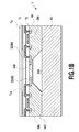
- the sensor chip 1 comprises: a main body provided with the plurality of pressure detection elements 32GR1, 32GR2, 32GR3, and 32GR4 and formed into a substantially rectangular shape with silicon, for example; a circuit layer 72 which is formed on an upper end surface of the main body and lead to the formation of a processing circuit; an insulation film layer as a second layer to be laminated on an upper surface of the circuit layer 72 that serves as a first layer; a shield layer 71 made of aluminum and formed on the insulation film layer; and a protection layer 76 to protect an upper portion of the shield layer 71.
- the main body comprises a fixed portion 64C coming into contact with and being supported by the glass layer 80, and a movable portion 64B.
- the thin movable portion 64B is integrally formed at a central part of the fixed portion 64C located at a position corresponding to a central part of the above-described diaphragm 16.
- a recessed portion 64A to be kept at a predetermined degree of vacuum is formed between the movable portion 64B and the glass layer 80.
- the pressure detection elements 32GR1, 32GR2, 32GR3, and 32GR4 are formed at four positions at regular intervals on a common circumference, for example, in such a way as to constitute a Wheatstone bridge circuit.
- the pressure detection elements 32GR1, 32GR2, 32GR3, and 32GR4 only need to be laid out in such a way as to constitute the Wheatstone bridge circuit, and are therefore not limited to the above-mentioned example.
- the layouts of the pressure detection elements 32GR1, 32GR2, 32GR3, and 32GR4 do not always have to be disposed at regular intervals on the common circumference.
- a circuit including MOSFETs metal-oxide-semiconductor field effect transistors
- MOSFETs metal-oxide-semiconductor field effect transistors
- gates 38A and 38B as well as drains and sources made of polysilicon, and the like
- a conductive layer made of aluminum is formed in the circuit layer 72 in such a way as to be electrically connected to the pressure detection elements 32GR1 to 32GR4 through a conductive layer made of aluminum.
- Vcc metal-oxide-semiconductor field effect transistors
- an output voltage Vout proportional to a pressure acting on the movable portion 64B is obtained between two connection ends, i.e. a connection end between the pressure detection element 32GR2 and the pressure detection element 32GR3 and a connection end between the pressure detection element 32GR1 and the pressure detection element 32GR4.
- the rectangular shield layer 71 made of aluminum, for example, is formed in a predetermined region (a shaded area) of the above-described insulation film layer located immediately above the conductive layer and the gates 38A and 38B.
- the shield layer 71 has an opening 71a at a position immediately above the pressure detection elements 32GR1, 32GR2, 32GR3, and 32GR4.
- the shield layer 71 constituting a shield electrode is grounded through a resistor 46.
- the resistor 46 may be configured as a wiring conductive layer for connecting the shield layer 71 to another region, for example.
- a wiring layer may be a resistor made of a material such as polysilicon, which is different from the material of the shield layer 71.
- the wiring conductive layer may be formed as a conductor pattern 80 as shown in the enlarged view of Fig. 7 .
- the conductor pattern 80 has a predetermined thickness T and a predetermined width W, and is formed into a shape of a rectangular wave by using the same material as the material of the shield layer 71, for example. It is to be noted that the shape of the conductor pattern 80 is not limited to the above-mentioned example and may, of course, be formed into any other shapes such as a fret pattern and a scroll pattern.
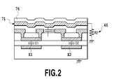
- FIG. 2 schematically shows a representative relation between the above-described shield electrode and electrodes E1 and E2 that are formed on an aluminum layer forming capacitors C1 and C2. the movable portion 64B and the fixed portion 64C are also grounded.
- a resistance value R2 of the resistor 46 is set to a substantially small value as compared to a resistance value of the above-mentioned silicone oil as the pressure transmission medium.
- the resistance value R2 of the resistor 46 is set in a range from 10 ⁇ to 1 M ⁇ inclusive, for example, or preferably in a range from 1 k ⁇ to 100 k ⁇ inclusive.
- an attenuation of a signal is determined by a relation between capacitance of a capacitor and a resistance value. When the resistance value R2 is below 1 k ⁇ , it is not possible to secure a sufficient attenuation for a noise countermeasure if the capacitance of the capacitor is small.
- the resistance value R2 of the resistor 46 is set preferably in the range from 1 k ⁇ to 100 k ⁇ inclusive.
- ⁇ resistivity
- L is a total length of a belt-like piece
- W is a width thereof (see Fig. 7 )
- T is a thickness thereof.
- respective values of the resistivity, the total length, the width, and the thickness of the conductor pattern 80 are appropriately selected such that the resistance value R2 falls in the range from 10 ⁇ to 1 M ⁇ inclusive.
- the resistor 46 is effective as an EMC countermeasure even in the case where a resonance circuit is formed from wiring of the shield electrode as inductance L1 and a capacitor C3 formed between an output voltage line (the aluminum layer) and the shield electrode as shown in Fig. 3 , for example.
- the aforementioned EMC countermeasure is not limited to this example.
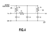
- resistors 48 and 50 having predetermined resistance values R3 and R4, respectively, may be provided in parallel between an input voltage line and the shield layer 71 that constitutes the shield electrode as shown in Fig. 4 , for instance.
- Each of the resistance values R3 and R4 is set in the range from 10 ⁇ to 1 M ⁇ inclusive, for example, or preferably in the range from 1 k ⁇ to 100 k ⁇ inclusive.
- the attenuation of the signal is usually determined by the relation between the capacitance of the capacitor and the resistance value.
- each of the resistance values R3 and R4 of the resistors 48 and 50 is set preferably in the range from 1 k ⁇ to 100 k ⁇ inclusive.
- the inventors of the present application have confirmed that the resistors 48 and 50 are each effective as the EMC countermeasure even in the case where the resonance circuit is formed from the capacitor C4 that is formed between the ground line (GND) and the shield electrode as described above. Note that illustration of the output voltage line is omitted in Fig. 4 .
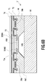
- a sensor chip 1' which is used in a second embodiment of a pressure sensor and a sensor unit including the same according to the present invention, is schematically illustrated in Fig. 6A and Fig. 6B together with a glass layer.
- the shield layer 71 has the opening 71a at the position immediately above the pressure detection elements 32GR1, 32GR2, 32GR3, and 32GR4.
- a shield layer 73 made of polysilicon is further formed inside the opening 71a at a position immediately above the pressure detection elements 32GR1, 32GR2, 32GR3, and 32GR4.
- the shield layer 73 constituting a shield electrode is formed in a substantially rectangular region (a shaded area) inside the opening 71a of the shield layer 71 and immediately above the pressure detection elements 32GR1, 32GR2, 32GR3, and 32GR4. At that time, the shield layer 73 is formed in such a way as to be located on the substantially common plane inside the opening 71a of the shield layer 71.
- the shield layer 73 constituting the shield electrode is also grounded through the above-described resistor 46.
- the shield layer 73 is not limited to the above-mentioned example.
- the shield layer 73 does not have to be located in the insulation film layer on substantially common plane with the plane of the shield layer 71, but may instead be formed at a position lower than the aforementioned position.
- each of the pressure detection elements is in no danger of degradation in sensitivity and linearity. Add to this, each of the pressure detection elements is in no danger of deterioration in temperature characteristic.
Landscapes
- Physics & Mathematics (AREA)
- General Physics & Mathematics (AREA)
- Electromagnetism (AREA)
- Measuring Fluid Pressure (AREA)
- Pressure Sensors (AREA)
Applications Claiming Priority (2)
| Application Number | Priority Date | Filing Date | Title |
|---|---|---|---|
| JP2012230043 | 2012-10-17 | ||
| PCT/JP2013/006124 WO2014061263A1 (ja) | 2012-10-17 | 2013-10-15 | 圧力センサおよび、それを備えるセンサユニット |
Publications (3)
| Publication Number | Publication Date |
|---|---|
| EP2910918A1 true EP2910918A1 (de) | 2015-08-26 |
| EP2910918A4 EP2910918A4 (de) | 2016-07-13 |
| EP2910918B1 EP2910918B1 (de) | 2018-07-25 |
Family
ID=50487842
Family Applications (1)
| Application Number | Title | Priority Date | Filing Date |
|---|---|---|---|
| EP13847081.0A Active EP2910918B1 (de) | 2012-10-17 | 2013-10-15 | Drucksensor und sensoreinheit mit drucksensor |
Country Status (5)
| Country | Link |
|---|---|
| US (1) | US9733142B2 (de) |
| EP (1) | EP2910918B1 (de) |
| JP (1) | JP5877248B2 (de) |
| CN (1) | CN104736983B (de) |
| WO (1) | WO2014061263A1 (de) |
Cited By (1)
| Publication number | Priority date | Publication date | Assignee | Title |
|---|---|---|---|---|
| US9733142B2 (en) | 2012-10-17 | 2017-08-15 | Kabushiki Kaisha Saginomiya Seisakusho | Pressure sensor, and sensor unit provided with same |
Families Citing this family (15)
| Publication number | Priority date | Publication date | Assignee | Title |
|---|---|---|---|---|
| US9557237B2 (en) * | 2013-11-18 | 2017-01-31 | Sensata Technologies, Inc. | MEMS pressure sensor field shield layout for surface charge immunity in oil filled packaging |
| US9915577B2 (en) | 2014-12-02 | 2018-03-13 | Sensata Technologies, Inc. | Case isolated oil filled MEMS pressure sensor |
| JP2017067463A (ja) * | 2015-09-28 | 2017-04-06 | セイコーエプソン株式会社 | 圧力センサー、高度計、電子機器および移動体 |
| JP2017220081A (ja) * | 2016-06-09 | 2017-12-14 | 富士電機株式会社 | センサ装置、センサシステムおよび測定方法 |
| CN106802199A (zh) * | 2016-12-27 | 2017-06-06 | 吴中区穹窿山德毅新材料技术研究所 | 新型传感器 |
| JP6776143B2 (ja) * | 2017-02-03 | 2020-10-28 | 横河電機株式会社 | 水位計測システム |
| CN109786316B (zh) * | 2017-11-10 | 2020-12-15 | 中芯国际集成电路制造(上海)有限公司 | 半导体器件、制造方法和电子设备 |
| JP6786469B2 (ja) * | 2017-11-30 | 2020-11-18 | 株式会社鷺宮製作所 | 圧力センサのシールド構造、および、それを備える圧力センサ |
| JP6718855B2 (ja) * | 2017-11-30 | 2020-07-08 | 株式会社鷺宮製作所 | 圧力センサのシールド構造、および、それを備える圧力センサ |
| JP6992482B2 (ja) | 2017-12-18 | 2022-01-13 | 富士電機株式会社 | 圧力センサ |
| USD970457S1 (en) * | 2018-08-21 | 2022-11-22 | Mitsubishi Electric Corporation | Capacitive sensor |
| EP3770112A1 (de) * | 2019-07-22 | 2021-01-27 | Infineon Technologies AG | Drucksensor |
| DE102020118313B4 (de) * | 2020-07-10 | 2023-10-05 | Vega Grieshaber Kg | Kanalstrukturen zur Optimierung der Membranfunktion von ölgefüllten Drucksensoren |
| US11629989B1 (en) | 2021-10-18 | 2023-04-18 | Fluid Management, Inc. | Level sensing for dispenser canisters |
| CN119340529A (zh) * | 2024-12-17 | 2025-01-21 | 深圳市瑞之辰科技有限公司 | 密封型金属封装传感器及电池 |
Family Cites Families (39)
| Publication number | Priority date | Publication date | Assignee | Title |
|---|---|---|---|---|
| JPH02198198A (ja) * | 1989-01-27 | 1990-08-06 | Cmk Corp | 電磁波シールド層を備えるプリント配線板 |
| JP2777747B2 (ja) * | 1990-11-26 | 1998-07-23 | 東亞合成株式会社 | 電磁波シールド層を有するプリント抵抗器内蔵多層プリント回路板 |
| US5589810A (en) * | 1991-03-28 | 1996-12-31 | The Foxboro Company | Semiconductor pressure sensor and related methodology with polysilicon diaphragm and single-crystal gage elements |
| US5231301A (en) * | 1991-10-02 | 1993-07-27 | Lucas Novasensor | Semiconductor sensor with piezoresistors and improved electrostatic structures |
| US5632854A (en) * | 1995-08-21 | 1997-05-27 | Motorola, Inc. | Pressure sensor method of fabrication |
| DE69922727T2 (de) * | 1998-03-31 | 2005-12-15 | Hitachi, Ltd. | Kapazitiver Druckwandler |
| US6278167B1 (en) * | 1998-08-14 | 2001-08-21 | Infineon Technologies Ag | Semiconductor sensor with a base element and at least one deformation element |
| FR2786564B1 (fr) * | 1998-11-27 | 2001-04-13 | Commissariat Energie Atomique | Capteur de pression a membrane comportant du carbure de silicium et procede de fabrication |
| US6229190B1 (en) * | 1998-12-18 | 2001-05-08 | Maxim Integrated Products, Inc. | Compensated semiconductor pressure sensor |
| JP2002101836A (ja) * | 2000-09-27 | 2002-04-09 | Yasumasa Morita | 海洋深層水を用いた麺及びパン |
| JP4356238B2 (ja) * | 2000-12-25 | 2009-11-04 | 株式会社デンソー | 圧力センサ |
| US20040232503A1 (en) * | 2001-06-12 | 2004-11-25 | Shinya Sato | Semiconductor device and method of producing the same |
| JP3987386B2 (ja) | 2001-11-20 | 2007-10-10 | 株式会社鷺宮製作所 | 圧力センサ |
| JP4027655B2 (ja) * | 2001-12-10 | 2007-12-26 | 株式会社不二工機 | 圧力センサ装置 |
| JP2003315193A (ja) * | 2002-04-24 | 2003-11-06 | Denso Corp | 圧力センサ |
| US6952042B2 (en) * | 2002-06-17 | 2005-10-04 | Honeywell International, Inc. | Microelectromechanical device with integrated conductive shield |
| CN1739014B (zh) * | 2003-01-30 | 2010-05-05 | 株式会社藤仓 | 半导体压力传感器及其制造方法 |
| JP2005037310A (ja) * | 2003-07-18 | 2005-02-10 | Fuji Koki Corp | 圧力センサ |
| JP2007502416A (ja) * | 2003-08-11 | 2007-02-08 | アナログ デバイシーズ インク | 容量型センサ |
| JP3847281B2 (ja) * | 2003-08-20 | 2006-11-22 | 株式会社山武 | 圧力センサ装置 |
| JP4774678B2 (ja) * | 2003-08-29 | 2011-09-14 | 富士電機株式会社 | 圧力センサ装置 |
| JP2006078417A (ja) * | 2004-09-13 | 2006-03-23 | Toyoda Mach Works Ltd | 圧力センサ |
| JP4548066B2 (ja) * | 2004-09-24 | 2010-09-22 | 株式会社デンソー | 圧力センサ |
| US7159467B2 (en) * | 2004-10-18 | 2007-01-09 | Silverbrook Research Pty Ltd | Pressure sensor with conductive ceramic membrane |
| US7884432B2 (en) * | 2005-03-22 | 2011-02-08 | Ametek, Inc. | Apparatus and methods for shielding integrated circuitry |
| JP4421511B2 (ja) * | 2005-05-30 | 2010-02-24 | 三菱電機株式会社 | 半導体圧力センサ |
| US7622782B2 (en) * | 2005-08-24 | 2009-11-24 | General Electric Company | Pressure sensors and methods of making the same |
| TWI286383B (en) * | 2005-12-23 | 2007-09-01 | Delta Electronics Inc | Semiconductor piezoresistive sensor and operation method thereof |
| JP4552883B2 (ja) * | 2006-04-19 | 2010-09-29 | 株式会社デンソー | 振動検出方法 |
| WO2008065883A1 (en) * | 2006-11-29 | 2008-06-05 | Fujikura Ltd. | Pressure sensor module |
| JP4965274B2 (ja) * | 2007-02-05 | 2012-07-04 | 三菱電機株式会社 | 圧力センサ |
| JP4600468B2 (ja) * | 2007-12-10 | 2010-12-15 | セイコーエプソン株式会社 | 半導体圧力センサ及びその製造方法、半導体装置並びに電子機器 |
| JP5309898B2 (ja) * | 2008-10-31 | 2013-10-09 | セイコーエプソン株式会社 | 圧力センサ装置 |
| JP2010155306A (ja) * | 2008-12-26 | 2010-07-15 | Panasonic Corp | Memsデバイス及びその製造方法 |
| TWI508194B (zh) * | 2009-01-06 | 2015-11-11 | 精材科技股份有限公司 | 電子元件封裝體及其製作方法 |
| US7775119B1 (en) * | 2009-03-03 | 2010-08-17 | S3C, Inc. | Media-compatible electrically isolated pressure sensor for high temperature applications |
| JP5853169B2 (ja) | 2010-12-15 | 2016-02-09 | パナソニックIpマネジメント株式会社 | 半導体圧力センサ |
| JP5691679B2 (ja) * | 2011-03-10 | 2015-04-01 | 東洋紡株式会社 | 積層体およびその製造方法 |
| WO2014061263A1 (ja) | 2012-10-17 | 2014-04-24 | 株式会社鷺宮製作所 | 圧力センサおよび、それを備えるセンサユニット |
-
2013
- 2013-10-15 WO PCT/JP2013/006124 patent/WO2014061263A1/ja not_active Ceased
- 2013-10-15 CN CN201380054448.5A patent/CN104736983B/zh active Active
- 2013-10-15 US US14/436,280 patent/US9733142B2/en active Active
- 2013-10-15 EP EP13847081.0A patent/EP2910918B1/de active Active
- 2013-10-15 JP JP2014541950A patent/JP5877248B2/ja active Active
Cited By (1)
| Publication number | Priority date | Publication date | Assignee | Title |
|---|---|---|---|---|
| US9733142B2 (en) | 2012-10-17 | 2017-08-15 | Kabushiki Kaisha Saginomiya Seisakusho | Pressure sensor, and sensor unit provided with same |
Also Published As
| Publication number | Publication date |
|---|---|
| JP5877248B2 (ja) | 2016-03-02 |
| EP2910918A4 (de) | 2016-07-13 |
| CN104736983B (zh) | 2017-05-31 |
| JPWO2014061263A1 (ja) | 2016-09-05 |
| WO2014061263A1 (ja) | 2014-04-24 |
| US9733142B2 (en) | 2017-08-15 |
| US20150285703A1 (en) | 2015-10-08 |
| CN104736983A (zh) | 2015-06-24 |
| EP2910918B1 (de) | 2018-07-25 |
Similar Documents
| Publication | Publication Date | Title |
|---|---|---|
| EP2910918B1 (de) | Drucksensor und sensoreinheit mit drucksensor | |
| JP4421511B2 (ja) | 半導体圧力センサ | |
| TWI648527B (zh) | 改良的壓力感測器結構 | |
| CN111351608B (zh) | 用于电容式压力传感器设备的微机械构件 | |
| TWI600887B (zh) | 一種改良的壓力感測器結構 | |
| US20160161435A1 (en) | Temperature and humidity sensor | |
| EP2878940B1 (de) | MEMS-Drucksensor-Feldabschirmungslayout für Oberflächenladungsimmunität in ölgefülltem Gehäuse | |
| JPH04106442A (ja) | 圧力センサ | |
| US10094724B2 (en) | Pressure sensor | |
| US9116063B2 (en) | Sensor unit | |
| US10962430B2 (en) | Pressure sensor | |
| JP7630671B2 (ja) | 圧力センサ | |
| CN222938651U (zh) | 压力传感器 | |
| USH606H (en) | Pressure sensor assembly | |
| US20190305472A1 (en) | Hermetic terminal and sensor unit | |
| EP4269973A1 (de) | Drucksensor | |
| JP2001208780A (ja) | 容量形分圧器 | |
| CN115356020A (zh) | 压力传感器装置 | |
| JP2009130378A (ja) | 電子装置 | |
| JPH01291415A (ja) | 半導体装置 |
Legal Events
| Date | Code | Title | Description |
|---|---|---|---|
| PUAI | Public reference made under article 153(3) epc to a published international application that has entered the european phase |
Free format text: ORIGINAL CODE: 0009012 |
|
| 17P | Request for examination filed |
Effective date: 20150416 |
|
| AK | Designated contracting states |
Kind code of ref document: A1 Designated state(s): AL AT BE BG CH CY CZ DE DK EE ES FI FR GB GR HR HU IE IS IT LI LT LU LV MC MK MT NL NO PL PT RO RS SE SI SK SM TR |
|
| AX | Request for extension of the european patent |
Extension state: BA ME |
|
| DAX | Request for extension of the european patent (deleted) | ||
| RIC1 | Information provided on ipc code assigned before grant |
Ipc: H01L 23/522 20060101ALI20160531BHEP Ipc: H01L 23/552 20060101ALI20160531BHEP Ipc: G01L 9/00 20060101AFI20160531BHEP |
|
| RA4 | Supplementary search report drawn up and despatched (corrected) |
Effective date: 20160609 |
|
| 17Q | First examination report despatched |
Effective date: 20170704 |
|
| GRAP | Despatch of communication of intention to grant a patent |
Free format text: ORIGINAL CODE: EPIDOSNIGR1 |
|
| INTG | Intention to grant announced |
Effective date: 20180301 |
|
| GRAS | Grant fee paid |
Free format text: ORIGINAL CODE: EPIDOSNIGR3 |
|
| GRAA | (expected) grant |
Free format text: ORIGINAL CODE: 0009210 |
|
| AK | Designated contracting states |
Kind code of ref document: B1 Designated state(s): AL AT BE BG CH CY CZ DE DK EE ES FI FR GB GR HR HU IE IS IT LI LT LU LV MC MK MT NL NO PL PT RO RS SE SI SK SM TR |
|
| REG | Reference to a national code |
Ref country code: GB Ref legal event code: FG4D |
|
| REG | Reference to a national code |
Ref country code: CH Ref legal event code: EP |
|
| REG | Reference to a national code |
Ref country code: AT Ref legal event code: REF Ref document number: 1022276 Country of ref document: AT Kind code of ref document: T Effective date: 20180815 |
|
| REG | Reference to a national code |
Ref country code: IE Ref legal event code: FG4D |
|
| REG | Reference to a national code |
Ref country code: DE Ref legal event code: R096 Ref document number: 602013040956 Country of ref document: DE |
|
| REG | Reference to a national code |
Ref country code: NL Ref legal event code: MP Effective date: 20180725 |
|
| REG | Reference to a national code |
Ref country code: LT Ref legal event code: MG4D |
|
| PG25 | Lapsed in a contracting state [announced via postgrant information from national office to epo] |
Ref country code: NL Free format text: LAPSE BECAUSE OF FAILURE TO SUBMIT A TRANSLATION OF THE DESCRIPTION OR TO PAY THE FEE WITHIN THE PRESCRIBED TIME-LIMIT Effective date: 20180725 |
|
| REG | Reference to a national code |
Ref country code: AT Ref legal event code: MK05 Ref document number: 1022276 Country of ref document: AT Kind code of ref document: T Effective date: 20180725 |
|
| PG25 | Lapsed in a contracting state [announced via postgrant information from national office to epo] |
Ref country code: IS Free format text: LAPSE BECAUSE OF FAILURE TO SUBMIT A TRANSLATION OF THE DESCRIPTION OR TO PAY THE FEE WITHIN THE PRESCRIBED TIME-LIMIT Effective date: 20181125 Ref country code: PL Free format text: LAPSE BECAUSE OF FAILURE TO SUBMIT A TRANSLATION OF THE DESCRIPTION OR TO PAY THE FEE WITHIN THE PRESCRIBED TIME-LIMIT Effective date: 20180725 Ref country code: RS Free format text: LAPSE BECAUSE OF FAILURE TO SUBMIT A TRANSLATION OF THE DESCRIPTION OR TO PAY THE FEE WITHIN THE PRESCRIBED TIME-LIMIT Effective date: 20180725 Ref country code: SE Free format text: LAPSE BECAUSE OF FAILURE TO SUBMIT A TRANSLATION OF THE DESCRIPTION OR TO PAY THE FEE WITHIN THE PRESCRIBED TIME-LIMIT Effective date: 20180725 Ref country code: AT Free format text: LAPSE BECAUSE OF FAILURE TO SUBMIT A TRANSLATION OF THE DESCRIPTION OR TO PAY THE FEE WITHIN THE PRESCRIBED TIME-LIMIT Effective date: 20180725 Ref country code: FI Free format text: LAPSE BECAUSE OF FAILURE TO SUBMIT A TRANSLATION OF THE DESCRIPTION OR TO PAY THE FEE WITHIN THE PRESCRIBED TIME-LIMIT Effective date: 20180725 Ref country code: GR Free format text: LAPSE BECAUSE OF FAILURE TO SUBMIT A TRANSLATION OF THE DESCRIPTION OR TO PAY THE FEE WITHIN THE PRESCRIBED TIME-LIMIT Effective date: 20181026 Ref country code: NO Free format text: LAPSE BECAUSE OF FAILURE TO SUBMIT A TRANSLATION OF THE DESCRIPTION OR TO PAY THE FEE WITHIN THE PRESCRIBED TIME-LIMIT Effective date: 20181025 Ref country code: BG Free format text: LAPSE BECAUSE OF FAILURE TO SUBMIT A TRANSLATION OF THE DESCRIPTION OR TO PAY THE FEE WITHIN THE PRESCRIBED TIME-LIMIT Effective date: 20181025 Ref country code: LT Free format text: LAPSE BECAUSE OF FAILURE TO SUBMIT A TRANSLATION OF THE DESCRIPTION OR TO PAY THE FEE WITHIN THE PRESCRIBED TIME-LIMIT Effective date: 20180725 |
|
| PG25 | Lapsed in a contracting state [announced via postgrant information from national office to epo] |
Ref country code: HR Free format text: LAPSE BECAUSE OF FAILURE TO SUBMIT A TRANSLATION OF THE DESCRIPTION OR TO PAY THE FEE WITHIN THE PRESCRIBED TIME-LIMIT Effective date: 20180725 Ref country code: AL Free format text: LAPSE BECAUSE OF FAILURE TO SUBMIT A TRANSLATION OF THE DESCRIPTION OR TO PAY THE FEE WITHIN THE PRESCRIBED TIME-LIMIT Effective date: 20180725 Ref country code: LV Free format text: LAPSE BECAUSE OF FAILURE TO SUBMIT A TRANSLATION OF THE DESCRIPTION OR TO PAY THE FEE WITHIN THE PRESCRIBED TIME-LIMIT Effective date: 20180725 |
|
| REG | Reference to a national code |
Ref country code: DE Ref legal event code: R097 Ref document number: 602013040956 Country of ref document: DE |
|
| PG25 | Lapsed in a contracting state [announced via postgrant information from national office to epo] |
Ref country code: RO Free format text: LAPSE BECAUSE OF FAILURE TO SUBMIT A TRANSLATION OF THE DESCRIPTION OR TO PAY THE FEE WITHIN THE PRESCRIBED TIME-LIMIT Effective date: 20180725 Ref country code: IT Free format text: LAPSE BECAUSE OF FAILURE TO SUBMIT A TRANSLATION OF THE DESCRIPTION OR TO PAY THE FEE WITHIN THE PRESCRIBED TIME-LIMIT Effective date: 20180725 Ref country code: CZ Free format text: LAPSE BECAUSE OF FAILURE TO SUBMIT A TRANSLATION OF THE DESCRIPTION OR TO PAY THE FEE WITHIN THE PRESCRIBED TIME-LIMIT Effective date: 20180725 Ref country code: ES Free format text: LAPSE BECAUSE OF FAILURE TO SUBMIT A TRANSLATION OF THE DESCRIPTION OR TO PAY THE FEE WITHIN THE PRESCRIBED TIME-LIMIT Effective date: 20180725 Ref country code: EE Free format text: LAPSE BECAUSE OF FAILURE TO SUBMIT A TRANSLATION OF THE DESCRIPTION OR TO PAY THE FEE WITHIN THE PRESCRIBED TIME-LIMIT Effective date: 20180725 |
|
| PG25 | Lapsed in a contracting state [announced via postgrant information from national office to epo] |
Ref country code: SK Free format text: LAPSE BECAUSE OF FAILURE TO SUBMIT A TRANSLATION OF THE DESCRIPTION OR TO PAY THE FEE WITHIN THE PRESCRIBED TIME-LIMIT Effective date: 20180725 Ref country code: DK Free format text: LAPSE BECAUSE OF FAILURE TO SUBMIT A TRANSLATION OF THE DESCRIPTION OR TO PAY THE FEE WITHIN THE PRESCRIBED TIME-LIMIT Effective date: 20180725 Ref country code: SM Free format text: LAPSE BECAUSE OF FAILURE TO SUBMIT A TRANSLATION OF THE DESCRIPTION OR TO PAY THE FEE WITHIN THE PRESCRIBED TIME-LIMIT Effective date: 20180725 |
|
| PLBE | No opposition filed within time limit |
Free format text: ORIGINAL CODE: 0009261 |
|
| REG | Reference to a national code |
Ref country code: CH Ref legal event code: PL |
|
| STAA | Information on the status of an ep patent application or granted ep patent |
Free format text: STATUS: NO OPPOSITION FILED WITHIN TIME LIMIT |
|
| GBPC | Gb: european patent ceased through non-payment of renewal fee |
Effective date: 20181025 |
|
| REG | Reference to a national code |
Ref country code: BE Ref legal event code: MM Effective date: 20181031 |
|
| PG25 | Lapsed in a contracting state [announced via postgrant information from national office to epo] |
Ref country code: MC Free format text: LAPSE BECAUSE OF FAILURE TO SUBMIT A TRANSLATION OF THE DESCRIPTION OR TO PAY THE FEE WITHIN THE PRESCRIBED TIME-LIMIT Effective date: 20180725 Ref country code: LU Free format text: LAPSE BECAUSE OF NON-PAYMENT OF DUE FEES Effective date: 20181015 |
|
| 26N | No opposition filed |
Effective date: 20190426 |
|
| REG | Reference to a national code |
Ref country code: IE Ref legal event code: MM4A |
|
| PG25 | Lapsed in a contracting state [announced via postgrant information from national office to epo] |
Ref country code: LI Free format text: LAPSE BECAUSE OF NON-PAYMENT OF DUE FEES Effective date: 20181031 Ref country code: CH Free format text: LAPSE BECAUSE OF NON-PAYMENT OF DUE FEES Effective date: 20181031 Ref country code: FR Free format text: LAPSE BECAUSE OF NON-PAYMENT OF DUE FEES Effective date: 20181031 Ref country code: SI Free format text: LAPSE BECAUSE OF FAILURE TO SUBMIT A TRANSLATION OF THE DESCRIPTION OR TO PAY THE FEE WITHIN THE PRESCRIBED TIME-LIMIT Effective date: 20180725 Ref country code: BE Free format text: LAPSE BECAUSE OF NON-PAYMENT OF DUE FEES Effective date: 20181031 |
|
| PG25 | Lapsed in a contracting state [announced via postgrant information from national office to epo] |
Ref country code: GB Free format text: LAPSE BECAUSE OF NON-PAYMENT OF DUE FEES Effective date: 20181025 Ref country code: IE Free format text: LAPSE BECAUSE OF NON-PAYMENT OF DUE FEES Effective date: 20181015 |
|
| PG25 | Lapsed in a contracting state [announced via postgrant information from national office to epo] |
Ref country code: MT Free format text: LAPSE BECAUSE OF NON-PAYMENT OF DUE FEES Effective date: 20181015 |
|
| PG25 | Lapsed in a contracting state [announced via postgrant information from national office to epo] |
Ref country code: TR Free format text: LAPSE BECAUSE OF FAILURE TO SUBMIT A TRANSLATION OF THE DESCRIPTION OR TO PAY THE FEE WITHIN THE PRESCRIBED TIME-LIMIT Effective date: 20180725 |
|
| PG25 | Lapsed in a contracting state [announced via postgrant information from national office to epo] |
Ref country code: PT Free format text: LAPSE BECAUSE OF FAILURE TO SUBMIT A TRANSLATION OF THE DESCRIPTION OR TO PAY THE FEE WITHIN THE PRESCRIBED TIME-LIMIT Effective date: 20180725 |
|
| PG25 | Lapsed in a contracting state [announced via postgrant information from national office to epo] |
Ref country code: CY Free format text: LAPSE BECAUSE OF FAILURE TO SUBMIT A TRANSLATION OF THE DESCRIPTION OR TO PAY THE FEE WITHIN THE PRESCRIBED TIME-LIMIT Effective date: 20180725 Ref country code: HU Free format text: LAPSE BECAUSE OF FAILURE TO SUBMIT A TRANSLATION OF THE DESCRIPTION OR TO PAY THE FEE WITHIN THE PRESCRIBED TIME-LIMIT; INVALID AB INITIO Effective date: 20131015 Ref country code: MK Free format text: LAPSE BECAUSE OF NON-PAYMENT OF DUE FEES Effective date: 20180725 |
|
| PGFP | Annual fee paid to national office [announced via postgrant information from national office to epo] |
Ref country code: DE Payment date: 20250902 Year of fee payment: 13 |