EP2907010B1 - Folie sowie körper mit einer solchen folie - Google Patents
Folie sowie körper mit einer solchen folie Download PDFInfo
- Publication number
- EP2907010B1 EP2907010B1 EP13776794.3A EP13776794A EP2907010B1 EP 2907010 B1 EP2907010 B1 EP 2907010B1 EP 13776794 A EP13776794 A EP 13776794A EP 2907010 B1 EP2907010 B1 EP 2907010B1
- Authority
- EP
- European Patent Office
- Prior art keywords
- film
- functional layer
- region
- layer
- contacting
- Prior art date
- Legal status (The legal status is an assumption and is not a legal conclusion. Google has not performed a legal analysis and makes no representation as to the accuracy of the status listed.)
- Active
Links
Images






Classifications
-
- G—PHYSICS
- G06—COMPUTING OR CALCULATING; COUNTING
- G06F—ELECTRIC DIGITAL DATA PROCESSING
- G06F3/00—Input arrangements for transferring data to be processed into a form capable of being handled by the computer; Output arrangements for transferring data from processing unit to output unit, e.g. interface arrangements
- G06F3/01—Input arrangements or combined input and output arrangements for interaction between user and computer
- G06F3/03—Arrangements for converting the position or the displacement of a member into a coded form
- G06F3/041—Digitisers, e.g. for touch screens or touch pads, characterised by the transducing means
- G06F3/044—Digitisers, e.g. for touch screens or touch pads, characterised by the transducing means by capacitive means
- G06F3/0443—Digitisers, e.g. for touch screens or touch pads, characterised by the transducing means by capacitive means using a single layer of sensing electrodes
-
- B—PERFORMING OPERATIONS; TRANSPORTING
- B29—WORKING OF PLASTICS; WORKING OF SUBSTANCES IN A PLASTIC STATE IN GENERAL
- B29C—SHAPING OR JOINING OF PLASTICS; SHAPING OF MATERIAL IN A PLASTIC STATE, NOT OTHERWISE PROVIDED FOR; AFTER-TREATMENT OF THE SHAPED PRODUCTS, e.g. REPAIRING
- B29C45/00—Injection moulding, i.e. forcing the required volume of moulding material through a nozzle into a closed mould; Apparatus therefor
- B29C45/14—Injection moulding, i.e. forcing the required volume of moulding material through a nozzle into a closed mould; Apparatus therefor incorporating preformed parts or layers, e.g. injection moulding around inserts or for coating articles
- B29C45/14639—Injection moulding, i.e. forcing the required volume of moulding material through a nozzle into a closed mould; Apparatus therefor incorporating preformed parts or layers, e.g. injection moulding around inserts or for coating articles for obtaining an insulating effect, e.g. for electrical components
-
- B—PERFORMING OPERATIONS; TRANSPORTING
- B29—WORKING OF PLASTICS; WORKING OF SUBSTANCES IN A PLASTIC STATE IN GENERAL
- B29C—SHAPING OR JOINING OF PLASTICS; SHAPING OF MATERIAL IN A PLASTIC STATE, NOT OTHERWISE PROVIDED FOR; AFTER-TREATMENT OF THE SHAPED PRODUCTS, e.g. REPAIRING
- B29C45/00—Injection moulding, i.e. forcing the required volume of moulding material through a nozzle into a closed mould; Apparatus therefor
- B29C45/14—Injection moulding, i.e. forcing the required volume of moulding material through a nozzle into a closed mould; Apparatus therefor incorporating preformed parts or layers, e.g. injection moulding around inserts or for coating articles
- B29C45/14778—Injection moulding, i.e. forcing the required volume of moulding material through a nozzle into a closed mould; Apparatus therefor incorporating preformed parts or layers, e.g. injection moulding around inserts or for coating articles the article consisting of a material with particular properties, e.g. porous, brittle
- B29C45/14811—Multilayered articles
-
- G—PHYSICS
- G01—MEASURING; TESTING
- G01R—MEASURING ELECTRIC VARIABLES; MEASURING MAGNETIC VARIABLES
- G01R27/00—Arrangements for measuring resistance, reactance, impedance, or electric characteristics derived therefrom
- G01R27/02—Measuring real or complex resistance, reactance, impedance, or other two-pole characteristics derived therefrom, e.g. time constant
- G01R27/26—Measuring inductance or capacitance; Measuring quality factor, e.g. by using the resonance method; Measuring loss factor; Measuring dielectric constants ; Measuring impedance or related variables
- G01R27/2605—Measuring capacitance
-
- G—PHYSICS
- G06—COMPUTING OR CALCULATING; COUNTING
- G06F—ELECTRIC DIGITAL DATA PROCESSING
- G06F3/00—Input arrangements for transferring data to be processed into a form capable of being handled by the computer; Output arrangements for transferring data from processing unit to output unit, e.g. interface arrangements
- G06F3/01—Input arrangements or combined input and output arrangements for interaction between user and computer
- G06F3/03—Arrangements for converting the position or the displacement of a member into a coded form
- G06F3/041—Digitisers, e.g. for touch screens or touch pads, characterised by the transducing means
- G06F3/0416—Control or interface arrangements specially adapted for digitisers
- G06F3/04164—Connections between sensors and controllers, e.g. routing lines between electrodes and connection pads
-
- H—ELECTRICITY
- H05—ELECTRIC TECHNIQUES NOT OTHERWISE PROVIDED FOR
- H05K—PRINTED CIRCUITS; CASINGS OR CONSTRUCTIONAL DETAILS OF ELECTRIC APPARATUS; MANUFACTURE OF ASSEMBLAGES OF ELECTRICAL COMPONENTS
- H05K1/00—Printed circuits
- H05K1/02—Details
- H05K1/0274—Optical details, e.g. printed circuits comprising integral optical means
-
- H—ELECTRICITY
- H05—ELECTRIC TECHNIQUES NOT OTHERWISE PROVIDED FOR
- H05K—PRINTED CIRCUITS; CASINGS OR CONSTRUCTIONAL DETAILS OF ELECTRIC APPARATUS; MANUFACTURE OF ASSEMBLAGES OF ELECTRICAL COMPONENTS
- H05K1/00—Printed circuits
- H05K1/02—Details
- H05K1/03—Use of materials for the substrate
- H05K1/0313—Organic insulating material
- H05K1/0353—Organic insulating material consisting of two or more materials, e.g. two or more polymers, polymer + filler, + reinforcement
- H05K1/0373—Organic insulating material consisting of two or more materials, e.g. two or more polymers, polymer + filler, + reinforcement containing additives, e.g. fillers
-
- H—ELECTRICITY
- H05—ELECTRIC TECHNIQUES NOT OTHERWISE PROVIDED FOR
- H05K—PRINTED CIRCUITS; CASINGS OR CONSTRUCTIONAL DETAILS OF ELECTRIC APPARATUS; MANUFACTURE OF ASSEMBLAGES OF ELECTRICAL COMPONENTS
- H05K1/00—Printed circuits
- H05K1/02—Details
- H05K1/11—Printed elements for providing electric connections to or between printed circuits
-
- H—ELECTRICITY
- H05—ELECTRIC TECHNIQUES NOT OTHERWISE PROVIDED FOR
- H05K—PRINTED CIRCUITS; CASINGS OR CONSTRUCTIONAL DETAILS OF ELECTRIC APPARATUS; MANUFACTURE OF ASSEMBLAGES OF ELECTRICAL COMPONENTS
- H05K1/00—Printed circuits
- H05K1/02—Details
- H05K1/11—Printed elements for providing electric connections to or between printed circuits
- H05K1/118—Printed elements for providing electric connections to or between printed circuits specially for flexible printed circuits, e.g. using folded portions
-
- H—ELECTRICITY
- H05—ELECTRIC TECHNIQUES NOT OTHERWISE PROVIDED FOR
- H05K—PRINTED CIRCUITS; CASINGS OR CONSTRUCTIONAL DETAILS OF ELECTRIC APPARATUS; MANUFACTURE OF ASSEMBLAGES OF ELECTRICAL COMPONENTS
- H05K1/00—Printed circuits
- H05K1/18—Printed circuits structurally associated with non-printed electric components
- H05K1/181—Printed circuits structurally associated with non-printed electric components associated with surface mounted components
-
- H—ELECTRICITY
- H05—ELECTRIC TECHNIQUES NOT OTHERWISE PROVIDED FOR
- H05K—PRINTED CIRCUITS; CASINGS OR CONSTRUCTIONAL DETAILS OF ELECTRIC APPARATUS; MANUFACTURE OF ASSEMBLAGES OF ELECTRICAL COMPONENTS
- H05K1/00—Printed circuits
- H05K1/18—Printed circuits structurally associated with non-printed electric components
- H05K1/189—Printed circuits structurally associated with non-printed electric components characterised by the use of flexible or folded printed circuits
-
- H—ELECTRICITY
- H05—ELECTRIC TECHNIQUES NOT OTHERWISE PROVIDED FOR
- H05K—PRINTED CIRCUITS; CASINGS OR CONSTRUCTIONAL DETAILS OF ELECTRIC APPARATUS; MANUFACTURE OF ASSEMBLAGES OF ELECTRICAL COMPONENTS
- H05K2201/00—Indexing scheme relating to printed circuits covered by H05K1/00
- H05K2201/01—Dielectrics
- H05K2201/0104—Properties and characteristics in general
- H05K2201/0108—Transparent
-
- H—ELECTRICITY
- H05—ELECTRIC TECHNIQUES NOT OTHERWISE PROVIDED FOR
- H05K—PRINTED CIRCUITS; CASINGS OR CONSTRUCTIONAL DETAILS OF ELECTRIC APPARATUS; MANUFACTURE OF ASSEMBLAGES OF ELECTRICAL COMPONENTS
- H05K2201/00—Indexing scheme relating to printed circuits covered by H05K1/00
- H05K2201/05—Flexible printed circuits [FPCs]
- H05K2201/053—Tails
-
- H—ELECTRICITY
- H05—ELECTRIC TECHNIQUES NOT OTHERWISE PROVIDED FOR
- H05K—PRINTED CIRCUITS; CASINGS OR CONSTRUCTIONAL DETAILS OF ELECTRIC APPARATUS; MANUFACTURE OF ASSEMBLAGES OF ELECTRICAL COMPONENTS
- H05K2201/00—Indexing scheme relating to printed circuits covered by H05K1/00
- H05K2201/10—Details of components or other objects attached to or integrated in a printed circuit board
- H05K2201/10007—Types of components
- H05K2201/10151—Sensor
Definitions
- the invention relates to a film which has at least one electrical or one electronic functional layer.
- at least one electrical and / or electronic component is provided in a functional area of the functional layer;
- at least one electrical connection is provided, which is galvanically coupled to at least one component, namely is galvanically coupled in the functional layer, via (contact) connections in the same.
- the foil has a contacting tab which at least partially provides the contacting region.
- Such a film may, for example, provide touchpad functionality; Then it has capacitive elements and can also be labeled as a sensor foil. Alternatively (or additionally), the foil may carry light emitting diode elements (such as organic light emitting diodes).
- Such films can be fed to a purpose without further action.
- a film which is in particular a plastic part in order to support the film and thus stabilize and protect it from damage.
- the body can then be used in a device as a finished component.
- a common measure to integrate a film in such a body is to inject the film behind.
- annular potentiometric touch sensor which has a base substrate from which a contacting tab on which the conductive structure continues.
- the invention also relates to a body, namely a plastic part.
- the plastic part is produced by an in-mold process.
- An in-mold process differentiates between in-mold labeling (IML) and in-mold decorating (IMD).
- IML in-mold labeling
- IMD in-mold decorating
- a film is back-injected.
- In-mold decoration uses a roll-to-roll process in which a film strip is passed through the injection mold.
- the foil tape has a carrier layer and a transfer layer.
- the transfer layer may become detached from the carrier layer. After the back molding, the transfer layer remains on the finished body, whereas the carrier layer is peeled off and transported on.
- the film is usually partially back-injected in such a way that the contacting region is at least partially free of the injection-molded plastic material.
- the Kunststoffleiterslasche the film is not back-injected or only in one approach area and thus can stand away and be led to a mating contact.
- the contacting tab must accordingly have a certain flexibility. It must be ensured that the contacting tab is not damaged as such, and that also contacting tracks (traces) are not damaged on themaschinetechnischslasche.
- a foil having at least one electrical or electronic functional layer, wherein at least one electrical and / or electronic component is provided in a functional region of the functional layer, and at least one electrical connection is provided in a contacting region of the at least one functional layer.
- the film has a Contacting tab which provides at least a portion of the contacting region, wherein on the functional layer in a transition region between the functional region and the contacting region, which transition region comprises at least a portion of the contacting tab, another layer in a thickness of at least 300 nm, preferably at least 1 micron , most preferably at least 7 microns, is applied and wherein the further layer comprises an electrically conductive material.
- a body which has a foil with at least one electrical or electronic functional layer, wherein at least one electrical and / or electronic component is provided in a functional area of the functional layer, and at least one functional area is at least one functional area electrical connection is provided, which is (in particular via connections in the functional layer) galvanically coupled to at least one component, wherein the body further comprises a plastic main material with which the film is partially connected so that the contacting region is at least partially free of plastic main material, so that a contacting tab protrudes, wherein on the functional layer in a transition region between the functional region and the contacting region, which comprises at least a partial region of the contacting tab, a further (material) layer in one Thickness of at least 300 nm, preferably at least 1 .mu.m, most preferably at least 7 .mu.m, is applied, wherein the further layer comprises an electrically conductive material and the body is partially connected to a plastic main material so that the contacting region at least partially free of plastic main material is,
- the present invention includes the idea to protect the contacting tab itself, as a whole, or the functional layer there from damage by the further layer. This is ensured in particular by the specified thickness of the further layer; This is particularly true when the electrical or electronic functional layer has a common thickness (eg between 10 and 50 nm) and / or when a substrate carrying the electrical or electronic functional layer has a corresponding typical thickness of some Having micrometers.
- the thickness of the further layer need not be limited, as long as the contacting strap remains sufficiently flexible. In the transition region, the back-injected area ends, so it starts the Kunststoffslasche.
- the shape of the tab itself ensures that the tab is not damaged so quickly when it is bent for the purpose of contacting with a mating contact. It is particularly advantageous that their width is reduced by at least 20%, preferably at least 40% of an initial width.
- the further layer has an electrically insulating material.
- the electrically insulating material prevents electrical flashovers on the electronic components and corresponding connecting lines.
- a suitable plastic material suitable for, for example, a substrate arranged below the electrical or electronic functional layer can be selected as the electrical insulating material.
- the electrically insulating material may comprise polymethyl (meth) acrylate (PMMA), polycarbonate and / or acrylonitrile butadiene styrene (ABS) and / or contain zinc oxide particles.
- PMMA polymethyl (meth) acrylate
- ABS acrylonitrile butadiene styrene
- the material may be applied in the form of a paint on the electrical functional layer as another layer, which ensures a particularly good cohesion.
- a substrate carries the electrical or electronic functional layer.
- the electrical insulating material then has a thickness deviating from the thickness of the substrate by at most +/- 10%. This embodiment is suitable if the electrically insulating material is the same material as the material used for the substrate or at least a comparable material, in particular with regard to its bending properties (modulus of elasticity). In a second embodiment, however, the electrically insulating material is harder than the substrate and therefore may be made thinner than the same.
- the same comprises an electrically conductive material. Its use is particularly suitable for electrical connection tracks (contact tracks) to protect against damage while supporting their operation.
- the electrically conductive material may in particular comprise conductive silver or carbon black. Such material can be imprinted particularly well.
- the electrically conductive material may in particular also be provided at a free end of the contacting tab and cover the electrical connection of the functional layer.
- the electrical connection beyond the layer thickness of the functional layer is reinforced just at the terminal end, so that when connecting to a mating contact effectively possible damage is avoided.
- a stiffening element may be provided on the side of the film facing away from the functional layer; such a reinforcing element can allow a secure connection of the contact area by contacting tab to a mating contact.
- the reinforcing element may consist of polyethylene terephthalate, polypropylene, polycarbonate or polyethylene naphthalate and in this case have a film thickness such that the total thickness of the remaining film with the reinforcing element in the range of 150 to 600 microns, z. B. is 300 microns.
- the further layer at least partially forming electrically conductive material may have a thickness from the interval of 1 to 15 microns, preferably 2 to 5 microns.
- electrically insulating material may be provided on the electrical functional layer, in particular only in certain regions, and electrically insulating material may be the electrically conductive material in the transitional region cover, but at the free end of justifyleiterslasche leave electrically conductive material.
- electrically insulating material may be the electrically conductive material in the transitional region cover, but at the free end of justifyleiterslasche leave electrically conductive material.
- the positive property of the electrically insulating material is associated with particularly good flexibility with a large layer thickness, with the advantage that the electrically conductive material reinforces the electrical functional layer, in particular protects it against abrasion at the free end.
- the electrical or electronic functional layer may also include such conductive tracks of metal, in particular the said materials, which are at least 100 microns wide. Such webs are well visible per se, but can be covered by a plastic material, such as in a separate decorative layer or by the substrate.
- the electrical functional layer comprises organic conductors such as PAni (polyaniline) or PEDOT / PSS (poly-3,4-ethylenedioxythiophene-polystyrenesulfonate).
- the electrical or electronic functional layer may comprise metal nanowires (eg of silver, copper or carbon nanotubes, carbon nanoparticles or graphene).
- combinations of said materials may be provided in the functional layer.
- the film comprises an already mentioned substrate which carries the further layers and in particular the functional layer.
- This substrate is made of plastic, in particular polyethylene terephthalate, polypropylene, polycarbonate, polyethylene naphthalate are suitable, preferably in a thickness from the interval of 12 to 150 microns, more preferably from the interval of 35 to 60 microns.
- the substrate is arranged in a variant between the functional layer and the plastic main material.
- the further layer lies on the side of the substrate facing away from the plastic main material on the functional layer.
- the functional layer is arranged between the substrate and the plastic main material, thus points to the injection molding material.
- the further layer between the substrate and the plastic main material is arranged, because it is indeed arranged on the functional layer.
- the functional layer in the contacting region to at least one connection preferably has such a contact path (connecting line) that widens toward the transition region.
- thermoplastic material is suitable as the main plastic material which is injection-molded; preference is given to acrylonitrile-butadiene-styrene (ABS), polycarbonate or polyamide.
- Such a plastic material may be colored so that one can not look into the interior of a housing bounded by the body.
- the plastic main material is transparent and thus allows a look through the body.
- the electrical or electronic functional layer of the film also acts transparently on the body. This effect can be achieved, for example, by the measure that the electrical or electronic functional layer has a multiplicity of conductive tracks which consist of metal, in particular silver, copper, aluminum, chromium or a metal alloy, and which have a width of between 1 micron and 40 microns (preferably between 5 microns and 25 microns), and at the same time have a distance of 10 microns to 5 mm from each other (preferably it is between 300 microns and 1 mm).
- the transparency of the electrical functional layer is at least 70%, preferably at least 80%, despite the metallic interconnects.
- These interconnects are preferably provided in a layer thickness from the interval of 10 to 150 nm, preferably from the interval of 30 to 60 nm.
- the body is provided in a preferred embodiment in such a manner that the film is back-injected with the plastic material; said compound of the film with the plastic main material thus takes place automatically during the process of back injection.
- the plastic main material (regionally) glued and / or (regionally) clamped and / or be laminated to the plastic material.
- an adhesion promoter layer may be provided at least on the part of the film which is injection-molded with plastic. In this way, a particularly good composite of the components plastic main material and film is provided.
- FIGS. 1 a and 1 b shown and denoted as a whole by 100 comprises a film 2 and injection molding material 3.
- the layer thicknesses of the individual components are not drawn to scale.
- the film 2 forms a film element which comprises a substrate 21 which adheres to the injection molding material 3 via an adhesion promoter layer (also referred to as "primer"), not shown in the figure. Not all of the film 2 is back-injected, but only a first region 20a of the film 2, whereas a second region 20b of the film 2 is not back-injected.
- the first area 20a is in particular a functional area and the second area 20b is a contacting area.
- the film 2 projects beyond the injection molding material 3.
- the film should comprise an electrical functional layer 22 on the substrate 21, for example in the form of capacitive elements to provide a touchpad functionality (so that the film 2 is a sensor film).
- the film 2 may carry light-emitting diode elements, for example organic light-emitting diodes ("OLED").
- the electrical functional layer 22 is preferably provided in the form of a metal layer which comprises silver, copper, aluminum, chromium or other metals or metal compounds and alloys.
- the layer thickness of this metal layer is between 10 and 150 nm, typically between 30 and 60 nm.
- the metal layer is in particular not continuous, but includes metallic interconnects in either a particularly regular or even irregular pattern, the interconnects each have a width of between 1 micron and 40 microns, preferably about 5 microns and 20 microns, and have a distance of between 100 microns and 5 mm from each other, preferably between 300 microns and 1 mm. Such metallic traces are not visible to the human eye without aids.
- the electrical functional layer 22 is transparent, although electrical components are provided at least in the form of electrical resistance elements and the like.
- the individual touch panels are formed by electrical traces, which are galvanically coupled together.
- the capacitive coupling takes place to other touch panels that are not galvanically coupled to these tracks and in turn have a plurality of metallic tracks, which are galvanically coupled together.
- metal traces to provide a touchpad function.
- Any conductive and semiconducting elements can contribute to the provision of electrical and electronic components.
- metal may be provided in the form of nanowires (such as silver, copper, or gold) or nanoparticles (such as silver, gold, or copper), carbon nanotubes or plastic nanoparticles may be provided, and finally, elements of graphene may also be provided be.
- organic conductors can PEDOT / PSS (poly-3,4-ethylenedioxythiophene-polystyrenesulfonate) or PAni (polyaniline).
- active electrical components such as organic light-emitting diodes, inorganic or organic photovoltaic cells, other display elements such as electroluminescent materials, electrochromic materials or electrophoretic materials may be provided, there may be integrated circuits or inorganic or organic memory. All of this can equally be used in the context of the present invention. This applies to all layer or layer structures and sequences described in this application.
- the contacting region 20b which has the shape of a contacting tab projecting away from the functional region 20a, comprises an electrical connection for the elements in the electrical functional layer.
- the contacting tab serves to connect the elements in the functional area 20a via a mating contact. It should also be avoided that when contacting a mating contact the electrical functional layer is damaged at the free end of justifyleiterslasche. Below are some measures shown how such damage can be prevented.
- electrically conductive material is applied to the electrical functional layer 22 as layer 23.
- the electrically conductive material is applied exactly where Also as part of the electrical functional layer 22 is already electrically conductive material.
- the material may be provided by applying an electrically conductive paste to the film 2 and may include conductive silver and / or carbon black.
- the application of the layer 23 takes place over the entire area in which the electrical functional layer 22 is present. Such application of the layer 23 protects both the transition region 20c and the free end 20d of the contacting tab.
- the prerequisite is that the layer thickness is sufficiently large, in particular between 1 .mu.m and 25 .mu.m, preferably between 6 and 10 .mu.m, z. B. 8 microns.
- the electrically conductive material ie in particular the electrically conductive paste
- the electrically conductive material is not applied over the entire surface, but only in the transition region 20c between the functional region 20a and the contacting region 20b (reference numeral 23a) and is also at the free end 20d provided (see reference numeral 23b).
- the transition region 20c there is protection during bending of the contacting tab, whereas in the end region 20d, the electrical connections are protected against damage when they come into contact with a mating contact.
- the application such that only there the electrically conductive material ie the electrically conductive paste
- the electrical functional layer comprises electrically conductive areas
- an electrically insulating material in the form of a separate lacquer layer 24 or else of an applied foil is provided on the electrical functional layer 22.
- the electrically insulating material does not extend as far as the free end 20d, but covers it It protects the electrically insulating material, which can be made of the same material as the substrate 21 (possible materials see below) Fig. 1a provided substantially in the same layer thickness as the substrate 21 and therefore keeps the Kunststofftechnikslasche still flexible, but at the same time avoids damage to the same or the electrical functional layer 22 in the transition region 20c.
- the electrically insulating layer 24 ' is made of a harder material than the substrate 21 and is thinner than it.
- the electrically insulating layer 24 is provided in the form of a film, which is fastened to the electrical functional layer 22 via a separate adhesive layer 27. Furthermore, a stiffening element 25 is located at the free end 20d. This extends into the region below the film 24 and the adhesive layer 27. It is particularly preferred in this variant if at the free end 20d additionally the conductive material, in particular carbon black in the section 23b as in Fig. 3a shown is provided.
- the embodiments according to Fig. 3a / b on the one hand and 4a to c On the other hand, one embodiment of the body 1 '"according to the invention can be combined with one another: It can be both conductive material as in Fig.
- Fig. 4e how out Fig. 4e can be seen, the adhesive layer 27 and the film 24 as well as the entire surface applied to the substrate 21 and the functional layer 22, in particular the dashed framed area in Fig. 4e ; only the free end 20d remains uncovered for the electrical contact.
- a stiffening element 25 on the side facing away from the electrical functional layer 22 of the substrate 21 may be attached.
- the portion 23b becomes capable of the electrically conductive paste, then the provision of the electrically insulating material 24 "ends, and then the reinforcing member starts 25th
- a fifth embodiment of the inventive body 1 according to iv Fig. 6a / b indicates the electrical functional layer 22 to the injection molding material 3. Since electrically insulating material 24 is applied to the functional layer 22, this electrically insulating layer 24 also faces the plastic material 3. Thus, it is not the substrate 21 adhered to the plastic material 3 but the electrically insulating material 24.
- the electrically insulating material 24 is in the form of a film, which is applied over the adhesive layer 27 on the functional layer 22, as described above with reference to FIG Fig. 4d / e explained.
- the conductive material in particular carbon black, in the section 23b as in FIG Fig. 3a shown is provided.
- an additional adhesion-promoting layer in particular a so-called primer layer or an adhesive layer, may also be provided between the plastic material 3 and the insulating material 24.
- the layer with the insulating material 24 itself may have adhesion-promoting properties.
- the substrate 21 is preferably made of plastic, for example polyethylene terephthalate, polypropylene, polycarbonate, polyethylene naphthalate, polyamide and similar materials, wherein the substrate 21 has a layer thickness of 12 to 600 .mu.m, in particular from 12 to 150 .mu.m, typically from 35 to 60 microns.
- the electrically insulating material 24 may be made of the same materials, wherein in one body the substrate 21 may be formed as a first material and for the electrically insulating material 24 another material may be selected from the above.
- the electrical functional layer 22 or the further layers 23, 23a, 23b, 24, 24 ' also a protective layer not shown in the figures, for example, of polyacrylate, polyvinyl chloride, polyvinyl acetate, polyurethane, polycarbonate, polyester, a Ethylenvinylacetatcopolymer, a hydrocarbon resin, chlorinated polyolefin, polyvinyl alcohol, melamine resin, ketone; Formaldehyde resin, polyvinylidene fluoride, epoxy resin, polystyrene, a polymeric cellulose compound, phenolic resin, polyamide, polymeric liquid crystals (LCP), urea resin and synthetic resin, or may comprise or may consist of combinations of these materials. This includes both thermal and radiation cured paint systems.
- the layer thickness of the protective layer can be between 2 and 6 microns.
- the protective layer also contributes in this case to avoid damage to themaschineticianslasche or the electrical functional layer.
- the primer material not shown in the figure may have a layer thickness of between 1 and 9 ⁇ m, preferably between 1 and 5 ⁇ m. It preferably consists of the following material: component Proportion of (%) methyl ethyl ketone 60 butyl 15 MMA polymer (Tg: 100 ° C) 07 MMA / EA copolymer (Tg: 35 ° C) 13 Silicate (SiO2) 05
- Tg is the glass transition temperature (glass transition temperature) of the respective component.
- thermoplastics are preferably polymethyl (meth) acrylate, acrylonitrile butadiene styrene, polycarbonate or polyamide.
- the injection molding material may be colored or transparent. It may comprise fillers such as glass fibers or carbon fibers, or may also be provided without fillers.
- the film 2 may be colored or transparent, with only areas colored and the others may be transparent, for.
- the functional area 20a may be colored and the contacting tab may be in the contacting area 20b transparent, and vice versa.
- the layers 23 and 24 may be completely or partially colored or completely or partially transparent.
Landscapes
- Engineering & Computer Science (AREA)
- General Engineering & Computer Science (AREA)
- Theoretical Computer Science (AREA)
- Microelectronics & Electronic Packaging (AREA)
- Physics & Mathematics (AREA)
- General Physics & Mathematics (AREA)
- Mechanical Engineering (AREA)
- Manufacturing & Machinery (AREA)
- Human Computer Interaction (AREA)
- Computer Networks & Wireless Communication (AREA)
- Laminated Bodies (AREA)
- Injection Moulding Of Plastics Or The Like (AREA)
- Internal Circuitry In Semiconductor Integrated Circuit Devices (AREA)
- Electroluminescent Light Sources (AREA)
Description
- Die Erfindung betrifft eine Folie, die zumindest eine elektrische oder eine elektronische Funktionsschicht aufweist. In einem Funktionsbereich der Funktionsschicht ist zumindest ein elektrisches und/oder elektronisches Bauelement bereitgestellt; in einem Kontaktierungsbereich der zumindest einen Funktionsschicht ist zumindest ein elektrischer Anschluss vorgesehen, der galvanisch mit zumindest einem Bauelement gekoppelt ist, nämlich in der Funktionsschicht galvanisch gekoppelt ist, über (Kontakt-) Verbindungen in derselben.
- Die Folie weist insbesondere eine Kontaktierungslasche auf, die den Kontaktierungsbereich zumindest zum Teil bereitstellt.
- Eine solche Folie kann beispielsweise eine Tastfeldfunktionalität bereitstellen; dann weist sie kapazitive Elemente auf und ist auch als Sensorfolie bezeichenbar. Alternativ (oder zusätzlich) kann die Folie Leuchtdiodenelemente tragen (etwa organische Leuchtdioden).
- Derartige Folien können für sich ohne weitere Maßnahme einem Einsatzzweck zugeführt werden. Es ist aber üblich, eine solche Folie in einen Körper zu integrieren, der insbesondere ein Kunststoffteil ist, um die Folie abzustützen und so zu stabilisieren und vor Beschädigung zu schützen. Der Körper kann dann auch in einem Gerät als fertiges Bauteil verwendet werden.
- Eine gängige Maßnahme, eine Folie in einen solchen Körper zu integrieren, besteht darin, die Folie zu hinterspritzen. Alternativ ist es auch möglich, die Folie auf einen bereits hergestellten Grundkörper aufzukleben, aufzuklemmen oder aufzulaminieren.
- Aus der
US 2006/0082556 ist ein ringförmiger potenziometrischer Touchsensor bekannt, der ein Grundsubstrat aufweist, von dem eine Kontaktierunglasche abgeht, auf der die leitfähige Struktur fortgeführt ist. - Aus der
EP 1100043 ist ein Touchsensor bekannt, bei dessen Montage ein Tail eingeklemmt und somit befestigt wird. - Entsprechend betrifft die Erfindung auch einen Körper, nämlich ein Kunststoffteil. Bevorzugt ist das Kunststoffteil durch ein In-Mould-Verfahren hergestellt.
- Bei einem In-Mould-Verfahren unterscheidet man zwischen dem In-Mould-Labeling (IML) und dem In-Mould-Dekorieren (IMD). Beim In-Mould-Verfahren wird insbesondere eine Folie hinterspritzt. Beim In-Mould-Labeling wird hierbei diese gesamte Folie Teil des fertigen Körpers bzw. Kunststoffteils. Bei der In-Mould-Dekoration verwendet man ein Rolle-zu-Rolle-Verfahren, bei dem ein Folienband durch die Spritzgussform hindurch geführt wird. Das Folienband weist eine Trägerschicht und eine Übertragungslage auf. Die Übertragungslage kann sich von der Trägerschicht lösen. Nach dem Hinterspritzen verbleibt die Übertragungslage an dem fertigen Körper, wohingegen die Trägerschicht abgelöst wird und weiter transportiert wird.
- Die Folie wird üblicherweise partiell so hinterspritzt, dass der Kontaktierungsbereich zumindest teilweise von dem spritzgegossenen Kunststoffmaterial frei ist. Die Kontaktierungslasche der Folie wird hierbei nicht oder nur in einem Ansatzbereich hinterspritzt und kann somit wegstehen und zu einem Gegenkontakt geführt werden. Die Kontaktierungslasche muss demgemäß eine gewisse Flexibilität haben. Es muss darauf geachtet werden, dass die Kontaktierungslasche als solche nicht beschädigt wird, und dass auch Kontaktierungsbahnen (Leiterbahnen) auf der Kontaktierungslasche nicht beschädigt werden.
- Es ist die Aufgabe der Erfindung, einen Weg aufzuzeigen, wie eine Folie der eingangs genannten Gattung und ein Körper, der insbesondere als Kunststoffteil durch ein In-Mould-Verfahren hergestellt ist, ausgestaltet wird, damit auf besonders zuverlässige Weise vermieden wird, dass beim Kontaktieren Schäden auftreten.
- Die Aufgabe wird durch eine Folie mit zumindest einer elektrischen oder elektronischen Funktionsschicht gelöst, wobei in einem Funktionsbereich der Funktionsschicht zumindest ein elektrisches und/oder elektronisches Bauelement bereitgestellt ist, und wobei in einem Kontaktierungsbereich der zumindest einen Funktionsschicht zumindest ein elektrischer Anschluss vorgesehen ist, der (insbesondere über Verbindungen in der Funktionsschicht) galvanisch mit zumindest einem Bauelement gekoppelt ist, und wobei die Folie eine Kontaktierungslasche aufweist, die zumindest einen Teil des Kontaktierungsbereichs bereitstellt, wobei auf der Funktionsschicht in einem Übergangsbereich zwischen dem Funktionsbereich und dem Kontaktierungsbereich, welcher Übergangsbereich zumindest einen Teilbereich der Kontaktierungslasche umfasst, eine weitere Lage in einer Dicke von zumindest 300 nm, bevorzugt zumindest von 1 µm, ganz besonders bevorzugt zumindest von 7 µm, aufgebracht ist und wobei die weitere lage ein elektrisch leitfähiges Material umfasst.
- Die Aufgabe wird auch durch einen Körper gelöst, der eine Folie mit zumindest einer elektrischen oder einer elektronischen Funktionsschicht aufweist, wobei in einem Funktionsbereich der Funktionsschicht zumindest ein elektrisches und/oder elektronisches Bauelement bereitgestellt ist, und wobei in einem Kontaktierungsbereich der zumindest einen Funktionsschicht zumindest ein elektrischer Anschluss vorgesehen ist, der (insbesondere über Verbindungen in der Funktionsschicht) galvanisch mit zumindest einem Bauelement gekoppelt ist, wobei der Körper ferner ein Kunststoffhauptmaterial umfasst, mit dem die Folie partiell so verbunden ist, dass der Kontaktierungsbereich zumindest teilweise von Kunststoffhauptmaterial frei ist, so dass eine Kontaktierungslasche wegsteht, wobei auf der Funktionsschicht in einem Übergangsbereich zwischen dem Funktionsbereich und dem Kontaktierungsbereich, der zumindest einen Teilbereich der Kontaktierungslasche umfasst, eine weitere (Material-) Lage in einer Dicke von zumindest 300 nm, bevorzugt zumindest von 1 µm, ganz besonders bevorzugt zumindest von 7 µm, aufgebracht ist wobei die weitere Lage ein elektrisch leitfähiges Material umfasst und der Körper mit einem Kunststoffhauptmaterial partiell so verbunden ist, dass der Kontaktierungsbereich zumindest teilweise von Kunststoffhauptmaterial frei ist, so dass die Kontaktierungslasche wegsteht.
- Die vorliegende Erfindung beinhaltet die Idee, durch die weitere Lage die Kontaktierungslasche selbst, als Ganzes, oder die Funktionsschicht dort vor Beschädigung zu schützen. Dies ist insbesondere durch die angegebene Dicke der weiteren Lage gewährleistet; das gilt im besonderen Maße dann, wenn die elektrische oder elektronische Funktionsschicht eine gängige Dicke (von z. B. zwischen 10 und 50 nm) aufweist und/oder wenn ein Substrat, das die elektrische oder elektronische Funktionsschicht trägt, eine entsprechende typische Dicke von einigen Mikrometern aufweist. Nach oben muss der Dicke der weiteren Lage keine Grenze gesetzt werden, sofern die Kontaktierungslasche noch ausreichend flexibel bleibt. In dem Übergangsbereich endet gerade der hinterspritzte Bereich, es beginnt also die Kontaktierungslasche. Durch die weitere Lage ist genau an dieser empfindlichen Stelle dafür gesorgt, dass nicht oder zumindest in einem verringerten Maße Gefahr besteht, dass die Lasche ein- oder abgerissen wird oder die elektrische oder elektronische Funktionsschicht am Übergang von Kunststoffhauptmaterial zu einem von Kunststoffhauptmaterial freien Bereich beschädigt wird, z. B. Kontaktierungsbahnen eingerissen werden.
- Bei dem zweiten Aspekt, demgemäß sich die Lasche in einem Übergangsbereich von dem Funktionsbereich weg verjüngt, ist durch die Form der Lasche selber gewährleistet, dass die Lasche nicht so schnell beschädigt wird, wenn sie zum Zwecke des Kontaktierens mit einem Gegenkontakt gebogen wird. Dabei ist insbesondere vorteilhaft, dass sich ihre Breite um zumindest 20%, bevorzugt zumindest 40% einer anfänglichen Breite verringert.
- In einer Variante weist die weitere Lage ein elektrisch isolierendes Material auf. Das elektrisch isolierende Material verhindert elektrische Überschläge auf die elektronischen Bauelemente und entsprechende Verbindungsleitungen.
- Insbesondere kann als elektrisches Isolierungsmaterial ein geeignetes, etwa zu einem unter der elektrischen bzw. elektronischen Funktionsschicht angeordneten Substrat passendes Kunststoffmaterial ausgewählt werden.
- Beispielsweise kann das elektrisch isolierende Material Polymethyl(meth)acrylat (PMMA), Polycarbonat und/oder Acrylnitrilbutadienstyrol (ABS) umfassen und/oder Zinkoxidpartikel enthalten.
- Das Material kann in Form eines Lackes auf die elektrische Funktionsschicht als weitere Lage aufgetragen sein, was für einen besonders guten Zusammenhalt sorgt.
- Es kann aber auch in Form einer gesonderten Folie bereitgestellt sein, die in einem Herstellungsverfahren besonders leicht aufbringbar ist.
- Es kann vorgesehen sein, dass ein Substrat die elektrische oder elektronische Funktionsschicht trägt. In einer Ausführungsform weist dann das elektrische isolierende Material eine um höchstens +/- 10 % von der Dicke des Substrats abweichende Dicke auf. Diese Ausführungsform ist dann geeignet, wenn das elektrisch isolierende Material dasselbe Material ist wie das für das Substrat verwendete Material oder zumindest ein vergleichbares Material ist, insbesondere hinsichtlich seiner Biegeeigenschaften (Elastizitätsmodul). Bei einer zweiten Ausführungsform ist das elektrisch isolierende Material jedoch härter als das Substrat und kann daher dünner als selbiges ausgeführt sein.
- Bei einer zweiten Variante hinsichtlich des Aspektes der Bereitstellung der weiteren Lage umfasst selbige ein elektrisch leitfähiges Material. Dessen Einsatz ist insbesondere dazu geeignet, elektrische Verbindungsbahnen (Kontaktbahnen) vor Beschädigung zu schützen und gleichzeitig deren Funktionsweise zu unterstützen.
- Das elektrisch leitfähige Material kann insbesondere Leitsilber oder Carbon Black umfassen. Solches Material lässt sich besonders gut aufdrucken.
- Neben dem Vorsehen dieses elektrisch leitfähigen Materials in dem Übergangsbereich zwischen dem Funktionsbereich und dem Kontaktierungsbereich kann das elektrisch leitfähige Material insbesondere auch an einem freien Ende der Kontaktierungslasche bereitgestellt sein und den elektrischen Anschluss der Funktionsschicht bedecken. Hierdurch wird der elektrische Anschluss über die Schichtdicke der Funktionsschicht hinaus gerade an dem Anschlussende verstärkt, so dass beim Anschließen an einen Gegenkontakt wirkungsvoll eine mögliche Beschädigung vermieden wird.
- Als Zusatzmaßnahme zur Verstärkung des freien Endes der Lasche auf der Seite der elektrischen bzw. elektronischen Funktionsschicht kann ein Versteifungselement an der der Funktionsschicht abgewandten Seite der Folie vorgesehen sein; ein solches Verstärkungselement kann ein sicheres Anschließen des Kontaktbereiches per Kontaktierungslasche an einen Gegenkontakt ermöglichen. Das Verstärkungselement kann aus Polyethylenterephtalat, Polypropylen, Polycarbonat oder Polyethylennaphtalat bestehen und hierbei eine solche Foliendicke aufweisen, dass die Gesamtdicke aus der übrigen Folie mit dem Verstärkungselement im Bereich von 150 bis 600 µm liegt, z. B. 300 µm beträgt. Das die weitere Lage zumindest zum Teil bildende elektrisch leitfähige Material kann eine Dicke aus dem Intervall von 1 bis 15 µm aufweisen, vorzugsweise 2 bis 5 µm.
- Die beiden Varianten der Verwendung von elektrisch isolierendem Material und elektrisch leitfähigem Material für die weitere Lage schließen sich nicht gegenseitig aus: So kann elektrisch leitfähiges Material auf der elektrischen Funktionsschicht bereitgestellt sein, insbesondere nur bereichsweise, und elektrisch isolierendes Material das elektrisch leitfähige Material in dem Übergangsbereich bedecken, an dem freien Ende der Kontaktierungslasche aber elektrisch leitfähiges Material freilassen. Bei dieser Ausführungsform wird die positive Eigenschaft des elektrisch isolierenden Materials einer besonders guten Flexibilität bei großer Lagendicke verbunden mit dem Vorteil, dass das elektrisch leitfähige Material die elektrische Funktionsschicht verstärkt, insbesondere an dem freien Ende vor Abrieb schützt.
- Die elektrische bzw. elektronische Funktionsschicht kann auch solche leitfähigen Bahnen aus Metall, insbesondere den genannten Materialien umfassen, die mindestens 100 µm breit sind. Solche Bahnen sind an sich gut sichtbar, können aber durch ein Kunststoffmaterial, etwa in einer gesonderten Dekorlage oder durch das Substrat, verdeckt werden.
- In einer anderen Ausführungsform weist die elektrische Funktionsschicht organische Leiter wie PAni (Polyanilin) oder PEDOT/PSS (Poly-3.4-Ethylendioxythiophen-Polystyrolsulfonat) auf. Außerdem kann die elektrische bzw. elektronische Funktionsschicht Metall-Nanodrähte (z. B. aus Silber, Kupfer oder Kohlenstoff-Nanoröhrchen, Kohlenstoff-Nanopartikeln oder Graphen umfassen). Ferner können Kombinationen der genannten Materialien in der Funktionsschicht vorgesehen sein.
- Üblicherweise umfasst die Folie ein bereits erwähntes Substrat, welches die weiteren Schichten und insbesondere die Funktionsschicht trägt. Dieses Substrat besteht aus Kunststoff, wobei sich insbesondere Polyethylenterephtalat, Polypropylen, Polycarbonat, Polyethylennaphtalat eignen, vorzugsweise in einer Dicke aus dem Intervall von 12 bis 150 µm, besonders bevorzugt aus dem Intervall von 35 bis 60 µm.
- Das Substrat ist in einer Variante zwischen der Funktionsschicht und dem Kunststoffhauptmaterial angeordnet. In diesem Falle liegt die weitere Lage auf der dem Kunststoffhauptmaterial abgewandten Seite des Substrats auf der Funktionsschicht.
- In einer anderen Variante ist die Funktionsschicht zwischen dem Substrat und dem Kunststoffhauptmaterial angeordnet, weist also zu dem Spritzgussmaterial hin. In diesem Fall ist auch die weitere Lage zwischen dem Substrat und dem Kunststoffhauptmaterial angeordnet, weil sie ja auf der Funktionsschicht angeordnet ist.
- Bei dem zweiten Aspekt der Erfindung mit der sich verjüngenden Kontaktierungslasche weist bevorzugt die Funktionsschicht in dem Kontaktierungsbereich zu zumindest einem Anschluss eine solche Kontaktbahn (Verbindungsleitung) auf, die sich zu dem Übergangsbereich hin verbreitert. Dadurch, dass die Kontaktbahn im Übergangsbereich breiter ist als sonst, kann bei einer Biegebewegung bezüglich der Kontaktierungslasche vermieden werden, dass die Kontaktbahn als Ganzes unterbrochen wird.
- Als Kunststoffhauptmaterial, das spritzgegossen wird, eignet sich prinzipiell jeder thermoplastische Kunststoff, bevorzugt sind Acrylnitrilbutadienstyrol (ABS), Polycarbonat oder Polyamid.
- Ein solches Kunststoffmaterial kann gefärbt sein, damit man nicht in das Innere eines Gehäuses blicken kann, das von dem Körper begrenzt ist. Bei einer anderen bevorzugten Variante ist hingegen das Kunststoffhauptmaterial transparent und ermöglicht somit ein Hindurchschauen durch den Körper. Dies ist insbesondere dann möglich, wenn auch die elektrische bzw. elektronische Funktionsschicht der Folie an dem Körper transparent wirkt. Dieser Effekt ist beispielsweise durch die Maßnahme erzielbar, dass die elektrische bzw. elektronische Funktionsschicht eine Vielzahl von leitfähigen Bahnen (Leiterbahnen) aufweist, welche aus Metall, insbesondere aus Silber, Kupfer, Aluminium, Chrom oder aus einer Metalllegierung bestehen, und die eine Breite von zwischen 1 µm und 40 µm aufweisen (bevorzugt zwischen 5 µm und 25 µm), und die gleichzeitig einen Abstand von 10 µm bis 5 mm zueinander haben (bevorzugt liegt er zwischen 300 µm und 1 mm). Solche Leiterbahnen sind für das menschliche Auge nicht bzw. schwer auflösbar und können daher nicht einzeln erkannt werden. Die Transparenz der elektrischen Funktionsschicht beträgt mindestens 70 %, bevorzugt mindestens 80 % trotz der metallischen Leiterbahnen. Diese Leiterbahnen sind bevorzugt in einer Schichtdicke aus dem Intervall von 10 bis 150 nm, bevorzugt aus dem Intervall von 30 bis 60 nm bereitgestellt.
- Der Körper ist bei einer bevorzugten Ausführungsform auf eine solche Weise bereitgestellt, dass die Folie mit dem Kunststoffmaterial hinterspritzt ist; die genannte Verbindung der Folie mit dem Kunststoffhauptmaterial erfolgt also automatisch beim Vorgang des Hinterspritzens. Alternativ oder zusätzlich kann das Kunststoffhauptmaterial (bereichsweise) angeklebt und/oder (bereichsweise) angeklemmt und/oder auf das Kunststoffmaterial auflaminiert sein.
- Bei dem Körper kann zum Erleichtern des Spritzgießens eine Haftvermittlerschicht zumindest an dem mit Kunststoff hinterspritzten Teil der Folie vorgesehen sein. Auf diese Weise wird für einen besonders guten Verbund der Komponenten Kunststoffhauptmaterial und Folie gesorgt.
- Nachfolgend werden bevorzugte Ausführungsformen der Erfindung unter Bezug auf die Zeichen näher erläutert, in der
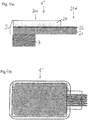
- Fig. 1a
- eine perspektivische Ansicht, und
- Fig. 1b
- eine Draufsicht eines Kunststoffteils als Körper nach dem Stand der Technik veranschaulicht,
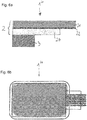
- Fig. 2a, 2b
- eine erste Ausführungsform der Erfindung veranschaulichen, wobei
Fig. 2b eine Draufsicht ist, und wobeiFig. 2a einen Schnitt in dem inFig. 2b strichliert umrandeten Bereich darstellt, - Fig. 3a, 3b
- eine zweite Ausführungsform der Erfindung veranschaulichen, wobei ebenfalls
Fig. 3a einen Schnitt darstellt undFig. 3b eine Draufsicht, - Fig. 4a, 4b
- eine dritte Ausführungsform der Erfindung veranschaulichen, wobei
Fig. 4a auch hier einen Schnitt darstellt undFig. 4b eine Draufsicht, wobei ferner - Fig. 4c
- einen Schnitt einer ersten Variante der dritten Ausführungsform gemäß
Fig. 4a veranschaulicht, und - Fig. 4d, 4e
- einen Schnitt bzw. eine Draufsicht einer zweiten Variante der dritten Ausführungsform gemäß
Fig. 4a veranschaulichen, - Fig. 5a
- eine vierte Ausführungsform der Erfindung in einem der
Fig. 4a entsprechenden Schnitt veranschaulicht und - Fig. 5b
- eine Erweiterung der Ausführungsform nach
Fig. 5a veranschaulicht, - Fig. 6a, 6b
- eine fünfte Ausführungsform der Erfindung veranschaulichen, wobei
Fig. 6a einen Schnitt darstellt undFig. 6b eine Draufsicht, - Fig. 6c
- einen Schnitt einer Variante der sechsten Ausführungsform der Erfindung veranschaulicht,
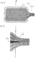
- Fig. 7a, 7b
- eine Draufsicht auf eine sechste Ausführungsform der Erfindung darstellen, wobei
Fig. 7b den inFig. 7a rechten Teilausschnitt vergrößert zeigt, und - Fig. 8
- einen Schnitt einer Abwandlung des Körpers der
Fig. 1 - 7b zeigt. - Ein in den
Figuren 1 a und 1 b gezeigter und im Ganzen mit 100 bezeichneter Körper umfasst eine Folie 2 und Spritzgussmaterial 3. Die Schichtdicken der einzelnen Komponenten sind nicht maßstäblich gezeichnet. Die Folie 2 bildet ein Folienelement, das ein Substrat 21 umfasst, welches über eine in der Figur nicht gezeigte Haftvermittlerschicht (auch als "Primer" bezeichnet) an dem Spritzgussmaterial 3 anhaftet. Es ist nicht die gesamte Folie 2 hinterspritzt, sondern lediglich ein erster Bereich 20a der Folie 2, wohingegen ein zweiter Bereich 20b der Folie 2 nicht hinterspritzt ist. Der erste Bereich 20a ist insbesondere ein Funktionsbereich und der zweite Bereich 20b ein Kontaktierungsbereich. In einem Übergangsbereich 20c steht die Folie 2 über das Spritzgussmaterial 3 hinaus. - Vorliegend soll die Folie eine elektrische Funktionsschicht 22 auf dem Substrat 21 umfassen, beispielsweise in Form von kapazitiven Elementen zur Bereitstellung einer Tastfeldfunktionalität (so dass die Folie 2 eine Sensorfolie ist). Alternativ oder zusätzlich ist es möglich, dass die Folie 2 Leuchtdiodenelemente trägt, z.B. organische Leuchtdioden ("OLED").
- Die elektrische Funktionsschicht 22 wird vorliegend bevorzugt in Form einer Metallschicht bereitgestellt, welche Silber, Kupfer, Aluminium, Chrom oder andere Metalle oder Metallverbindungen und -legierungen umfasst. Die Schichtdicke dieser Metallschicht beträgt zwischen 10 und 150 nm, typischerweise zwischen 30 und 60 nm. Die Metallschicht ist insbesondere nicht durchgängig, sondern umfasst metallische Leiterbahnen in einem entweder besonders regelmäßigen oder gerade unregelmäßigen Muster, wobei die Leiterbahnen jeweils eine Breite von zwischen 1 µm und 40 µm aufweisen, bevorzugt etwa 5 µm und 20 µm, und einen Abstand von zwischen 100 µm und 5 mm zueinander haben, bevorzugt von zwischen 300 µm und 1 mm. Solche metallischen Leiterbahnen sind mit dem menschlichen Auge ohne Hilfsmittel nicht erkennbar. Dadurch wirkt die elektrische Funktionsschicht 22 transparent, obwohl elektrische Bauelemente zumindest in Form von elektrischen Widerstandselementen und dergleichen bereitgestellt sind. Etwa bei einer Tastfeldfunktionalität sind die einzelnen Tastfelder durch elektrische Leiterbahnen gebildet, welche galvanisch miteinander gekoppelt sind. Die kapazitive Koppelung erfolgt zu anderen Tastfeldern, die nicht galvanisch mit diesen Leiterbahnen gekoppelt sind und ihrerseits eine Mehrzahl von metallischen Leiterbahnen aufweisen, die untereinander galvanisch miteinander gekoppelt sind.
- Die Erfindung ist nicht auf die Verwendung von metallischen Leiterbahnen zur Bereitstellung einer Tastfeldfunktion eingeschränkt. Jegliche leitenden und halbleitenden Elemente können zur Bereitstellung elektrischer und elektronischer Bauelemente beitragen. Beispielsweise kann Metall in Form von Nanodrähten (etwa aus Silber, Kupfer oder Gold) oder Nanopartikeln (etwa aus Silber, Gold oder Kupfer) bereitgestellt sein, es können Kohlenstoff-Nanoröhrchen oder Kunststoff-Nanopartikeln bereitgestellt sein, und schließlich können auch Elemente aus Graphen vorgesehen sein. Außerdem können organische Leiter aus PEDOT/PSS (Poly-3.4-Ethylendioxythiophen-Polystyrolsulfonat) oder aus PAni (Polyanilin) bereitgestellt sein. Insbesondere können aktive elektrische Bauteile wie beispielsweise organische Leuchtdioden, anorganische oder organische Photovoltaikzellen, andere Displayelemente wie etwa aus Elektrolumineszenzmaterialien, elektrochromen Materialien oder elektrophoretischen Materialien vorgesehen sein, es können integrierte Schaltungen oder anorganische oder organische Speicher vorgesehen sein. All dies kann im Rahmen der vorliegenden Erfindung gleichermaßen eingesetzt werden. Das gilt für alle in dieser Anmeldung beschriebenen Schicht- bzw. Lagenaufbauten und -abfolgen.
- Der Kontaktierungsbereich 20b, der die Form einer von dem Funktionsbereich 20a wegragenden Kontaktierungslasche hat, umfasst einen elektrischen Anschluss für die Elemente in der elektrischen Funktionsschicht.
- Durch das Abstehen der Kontaktierungslasche besteht die Gefahr, dass diese im Übergangsbereich zwischen dem Spritzgussmaterial 3 zum freien Raum einreißt, oder dass dort die elektrische Funktionsschicht beschädigt wird. Die Kontaktierungslasche dient zum Anschließen der Elemente in dem Funktionsbereich 20a über einen Gegenkontakt. Es soll auch vermieden werden, dass beim Kontaktieren an einen Gegenkontakt die elektrische Funktionsschicht am freien Ende der Kontaktierungslasche beschädigt wird.
Nachfolgend werden einige Maßnahmen aufgezeigt, wie solche Beschädigungen verhindert werden können. - Bei der ersten Ausführungsform des erfindungsgemäßen Körpers 1 ist auf die elektrische Funktionsschicht 22 elektrisch leitfähiges Material als Lage 23 aufgebracht. Das elektrisch leitfähige Material wird genau dort aufgebracht, wo sich auch als Teil der elektrischen Funktionsschicht 22 bereits elektrisch leitfähiges Material befindet.
- Das Material kann durch Aufbringen einer elektrischen leitfähigen Paste auf die Folie 2 bereitgestellt sein und Leitsilber und/oder Carbon Black umfassen bzw. sein. Das Aufbringen der Lage 23 erfolgt über den gesamten Bereich, in dem die elektrische Funktionsschicht 22 vorhanden ist. Durch ein solches Aufbringen der Lage 23 wird sowohl der Übergangsbereich 20c als auch das freie Ende 20d der Kontaktierungslasche geschützt. Voraussetzung ist, dass die Schichtdicke ausreichend groß ist, insbesondere zwischen 1 µm und 25 µm liegt, bevorzugt zwischen 6 und 10 µm liegt, z. B. 8 µm beträgt.
- Bei einer zweiten Ausführungsform des erfindungsgemäßen Körpers 1' ist das elektrisch leitfähige Material, also insbesondere die elektrisch leitfähige Paste, nicht vollflächig aufgebracht, sondern lediglich im Übergangsbereich 20c zwischen dem Funktionsbereich 20a und dem Kontaktierungsbereich 20b (Bezugszeichen 23a) und ist außerdem am freien Ende 20d vorgesehen (siehe das Bezugszeichen 23b). Im Übergangsbereich 20c besteht ein Schutz beim Biegen der Kontaktierungslasche, wo hingegen im Endbereich 20d die elektrischen Anschlüsse vor einem Beschädigtwerden beim Kontaktieren mit einem Gegenkontakt geschützt sind. Hierbei ist insbesondere in jedem Bereich, in dem das elektrisch leitfähige Material überhaupt aufgebracht ist (also im Übergangsbereich 20c und am freien Ende 20d) die Aufbringung dergestalt, dass nur dort das elektrisch leitfähige Material (also die elektrisch leitfähige Paste) aufgebracht wird, wo auch schon die elektrische Funktionsschicht elektrisch leitfähige Bereiche umfasst.
- Bei einer dritten Ausführungsform des erfindungsgemäßen Körpers 1" ist auf der elektrischen Funktionsschicht 22 ein elektrisch isolierendes Material in Form einer gesonderten Lackschicht 24 oder auch einer aufgebrachten Folie vorgesehen. Das elektrisch isolierende Material erstreckt sich jedoch gerade nicht bis zum freien Ende 20d hin, sondern erfasst lediglich den Übergangsbereich 20c. Damit schützt das elektrisch isolierende Material, das aus demselben Material bestehen kann wie das Substrat 21 (mögliche Materialien s. u.). Es ist bei der Ausführungsform gemäß
Fig. 1a im Wesentlichen in derselben Schichtendicke vorgesehen wie das Substrat 21 und hält daher die Kontaktierungslasche noch flexibel, vermeidet aber gleichzeitig eine Beschädigung derselben oder der elektrischen Funktionsschicht 22 im Übergangsbereich 20c. - Bei einer Variante gemäß
Fig. 4c ist die elektrisch isolierende Lage 24' aus einem härteren Material ausgebildet als das Substrat 21 und dafür dünner als selbiges vorgesehen. - Bei einer Variante gemäß
Fig. 4d /e ist die elektrisch isolierende Lage 24 in Form einer Folie bereitgestellt, die über eine gesonderte Kleberschicht 27 an der elektrischen Funktionsschicht 22 befestigt ist. Ferner befindet sich am freien Ende 20d ein Versteifungselement 25. Dieses erstreckt sich bis in den Bereich unterhalb der Folie 24 und der Kleberschicht 27. Besonders bevorzugt ist es bei dieser Variante, wenn am freien Ende 20d auch noch zusätzlich das leitfähige Material, insbesondere Carbon Black, in dem Abschnitt 23b wie inFig. 3a gezeigt, vorgesehen ist.
Die Ausführungsformen gemäßFig. 3a /b einerseits undFig.4a bis c andererseits lassen sich zu einer Ausführungsform des erfindungsgemäßen Körpers 1'" miteinander kombinieren: Es kann sowohl leitfähiges Material wie inFig. 3a gezeigt in den entsprechenden Bereichen als Abschnitte 23a und 23b vorgesehen sein, und der Abschnitt 23a, möglicherweise teilweise der Abschnitt 23 b, wird durch elektrisch isolierendes Material 24" bedeckt, wobei aber das freie Ende 20d freigelassen ist, damit eine elektrische Kontaktierung im Bereich des freien Endes 20d erfolgen kann. - Wie aus
Fig. 4e ersichtlich, sind die Klebeschicht 27 und die Folie 24 so gut wie vollflächig auf das Substrat 21 und die Funktionsschicht 22 aufgebracht, vergleiche insbesondere den gestrichelten umrahmten Bereich inFig. 4e ; lediglich das freie Ende 20d bleibt für die elektrische Kontaktierung unbedeckt. - Zusätzlich kann noch, wie in
Fig. 5b gezeigt, am freien Ende 20d ein Versteifungselement 25 auf der der elektrischen Funktionsschicht 22 abgewandten Seite des Substrats 21 angebracht sein. Wie durch die strichlierten Linien dargestellt, beginnt in Richtung von dem Spritzgussmaterial 3 weg (vergleiche den Pfeil P) zunächst der Abschnitt 23b in der Lage mit der elektrisch leitfähigen Paste, dann endet das Vorsehen des elektrisch isolierenden Materials 24", und dann beginnt das Verstärkungselement 25. - Bei einer fünften Ausführungsform des erfindungsgemäßen Körpers 1iv gemäß
Fig. 6a /b weist die elektrische Funktionsschicht 22 zu dem Spritzgussmaterial 3 hin. Da elektrisch isolierendes Material 24 auf der Funktionsschicht 22 aufgebracht ist, weist auch diese elektrisch isolierende Lage 24 zum Kunststoffmaterial 3 hin. Somit ist es nicht das Substrat 21, das an dem Kunststoffmaterial 3 haftet, sondern das elektrisch isolierende Material 24. - Bei einer Variante dieser Ausführungsform gemäß
Fig. 6c liegt das elektrisch isolierende Material 24 in Form einer Folie vor, die über die Kleberschicht 27 auf der Funktionsschicht 22 aufgebracht ist, wie oben anhand derFig. 4d /e erläutert. - Besonders bevorzugt ist es bei dieser Variante, wenn am freien Ende 20d auch noch zusätzlich das leitfähige Material, insbesondere Carbon Black, in dem Abschnitt 23b wie in
Fig. 3a gezeigt, vorgesehen ist. - Grundsätzlich wäre auch bei den beiden Varianten der fünften Ausführungsform gemäß
Fig. 6a/6b und6c das Vorsehen von elektrisch leitfähiger Paste auf der elektrischen Funktionsschicht 22 möglich, die dann ebenfalls zum Kunststoffmaterial 3 zeigen würde. - In den Ausführungsformen gemäß der
Fig. 6a/6b und6c kann insbesondere auch noch eine zusätzliche haftvermittelnde Schicht, insbesondere eine sogenannte Primer-Schicht oder eine Klebeschicht, zwischen dem Kunststoffmaterial 3 und dem isolierenden Material 24 vorgesehen sein. Alternativ kann auch die Schicht mit dem isolierenden Material 24 selbst haftvermittelnde Eigenschaften aufweisen. - Eine sechste Ausführungsform des erfindungsgemäßen Körpers 1 B zeigt die
Fig. 7a mit derFig. 7b : - Der Kontaktierungsbereich 20b' steht von dem Funktionsbereich 20a so weg wie im Stand der Technik gemäß
Fig. 1a/1b , es ist allerdings statt einer im Wesentlichen rechteckigen Lasche wie im Stand der Technik ein Sich-Verjüngen im Kontaktierungsbereich 20b' vorgesehen. Wie sich aus derFig. 7a und insbesondere auch der Vergrößerung gemäßFig. 7b ergibt, werden hier rechtwinklige Ecken als potentielle Einrißstellen wirksam vermieden. Elektrische Kontaktbahnen 26 verbreitern sich ebenfalls zumindest teilweise zum Funktionsbereich 20a hin, siehe insbesondere die mittige Kontaktierungsbahn 26a inFig. 7b . - Nach der Darstellung der unterschiedlichen Ausführungsformen für einen erfindungsgemäßen Körper folgen nun einige Detailangaben, insbesondere einiger wichtiger Werte.
- Das Substrat 21 besteht bevorzugt aus Kunststoff, beispielsweise Polyethylenterephtalat, Polypropylen, Polycarbonat, Polyethylennaphtalat, Polyamid and ähnlichen Materialien, wobei das Substrat 21 eine Schichtdicke von 12 bis 600 µm, insbesondere von 12 bis 150 µm, typischerweise von 35 bis 60 µm aufweist.
- Das elektrisch isolierende Material 24 kann aus denselben Materialien bestehen, wobei in einem Körper das Substrat 21 als erstes Material ausgebildet sein kann und für das elektrisch isolierende Material 24 ein anderes Material aus den oben genannten ausgewählt sein kann.
- Es kann auf der elektrischen Funktionsschicht 22 oder den weiteren Lagen 23, 23a, 23b, 24, 24' auch eine in den Figuren nicht gezeigte Schutzschicht vorgesehen sein, die beispielsweise aus Polyacrylat, Polyvinylchlorid, Polyvinylacetat, Polyurethan, Polycarbonat, Polyester, einem Ethylenvinylacetatcopolymer, einem Kohlenwasserstoffharz, chloriertem Polyolefin, Polyvinylalkohol, Melaminharz, Keton; Formaldehydharz, Polyvinylidenfluorid, Epoxitharz, Polystyrol, einer polymeren Zelluloseverbindung, Phenolharz, Polyamid, polymeren Flüssigkristallen (LCP), Harnstoffharz und Kunstharz bestehen kann oder diese Materialien umfassen kann, oder aus Kombinationen dieser Stoffe bestehen kann oder diese umfassen kann. Dies schließt sowohl thermische als auch strahlengehärtete Lacksysteme ein.
- Die Schichtdicke der Schutzschicht kann zwischen 2 und 6 µm liegen. Auch die Schutzschicht trägt in diesem Falle dazu bei, eine Beschädigung der Kontaktierungslasche bzw. der elektrischen Funktionsschicht zu vermeiden.
- Das in der Figur nicht gezeigte Haftvermittlermaterial (Primer) kann eine Schichtdicke von zwischen 1 und 9 µm, vorzugsweise von zwischen 1 und 5 µm haben. Es besteht vorzugsweise aus folgendem Material:
Komponente Anteil (%) Methylethylketon 60 Butylacetat 15 MMA Polymer (Tg: 100°C) 07 MMA/EA-Copolymer (Tg: 35°C) 13 Silikat (SiO2) 05 - Hierbei ist Tg die Glastemperatur (Einfriertemperatur) der jeweiligen Komponente.
- Als Spritzgussmaterial 3 können sämtliche thermoplastische Kunststoffe eingesetzt werden, bevorzugt sind dies Polymethyl(meth)acrylat, Acrylnitrilbutadienstyrol, Polycarbonat oder Polyamid.
- Das Spritzgussmaterial kann farbig oder transparent sein. Es kann Füllstoffe wie Glasfasern oder Karbonfasern umfassen, oder auch ohne Füllstoffe vorgesehen sein.
- Auch die Folie 2 kann farbig oder transparent sein, wobei auch nur Bereiche farbig und die anderen transparent sein können, z. B. kann der Funktionsbereich 20a farbig sein und die Kontaktierungslasche im Kontaktierungsbereich 20b transparent, und umgekehrt. Auch die Lagen 23 bzw. 24 können ganz oder bereichsweise farbig oder ganz oder bereichsweise transparent sein.
- Bei den bisher beschriebenen Ausführungsformen befindet sich unterhalb des Übergangsbereichs 20c zwischen dem Funktionsbereich 20a und dem Kontaktierungsbereich 20b immer eine Kante, weil dort das Kunststoffmaterial 3 endet.
- Ein Hinterspritzen kann jedoch auch so erfolgen, dass sich unterhalb der Kontaktierungslasche noch Kunststoffmaterial befindet, wie in
Fig. 8 angedeutet: In diesem Falle steht die Kontaktierungslasche zwar weg, sie könnte aber grundsätzlich auf das Kunststoffmaterial 3 aufgelegt werden. Dadurch können Vorteile beim Kontaktieren erzielt werden, etwa wenn das Kunststoffmaterial 3 in einem Gerät fest montiert werden soll und die Kontaktierungslasche 2 innerhalb des Geräts zu einem Gegenkontakt geführt werden soll.
Claims (15)
- Folie (2) mit zumindest einer elektrischen oder elektronischen Funktionsschicht (22), wobei in einem Funktionsbereich (20a, 20a') der Funktionsschicht (22) zumindest ein elektrisches und/oder elektronisches Bauelement bereitgestellt ist, und wobei in einem Kontaktierungsbereich (20b, 20b') der zumindest einen Funktionsschicht (22) zumindest ein elektrischer Anschluss vorgesehen ist, welcher galvanisch mit zumindest einem Bauelement gekoppelt ist und wobei die Folie (2) eine Kontaktierungslasche aufweist, die zumindest einen Teil des Kontaktierungsbereichs (20b, 20b') bereitstellt, wobei auf der Funktionsschicht (22) in einem Übergangsbereich (20c) zwischen dem Funktionsbereich (20a) und dem Kontaktierungsbereich (20b), der zumindest einen Teilbereich der Kontaktierungslasche umfasst, eine weitere Lage (23; 23a, 23b; 24; 24', 24") in einer Dicke von zumindest 300 nm und bevorzugt zumindest 1 µm, besonders bevorzugt von zumindest 7 µm aufgebracht ist, wobei die weitere Lage ein elektrisch leitfähiges Material (23; 23; 23b) umfasst.
- Folie (2) nach Anspruch 1,
bei der die weitere Lage ein elektrisch isolierendes Material (24, 24', 24") umfasst, welches insbesondere
Polymethyl(meth)acrylat, Polycarbonat und/oder Acrylnitrilbutadienstyrol umfasst und/oder Zinkoxidpartikel enthält. - Folie (2) nach Anspruch 2,
bei der das elektrisch isolierende Material (24, 24', 24") in Form eines Lacks bereitgestellt ist oder
in Form einer gesonderten Folie (24, 24'), welche insbesondere vermittels einer Klebstoffschicht (27) an der Funktionsschicht befestigt ist, bereitgestellt ist. - Folie (2), nach einem der Ansprüche 2 oder 3,
bei der ein Substrat (21) die elektrische oder elektronische Funktionsschicht (22) trägt und das elektrisch isolierende Material (24) eine um höchstens +/-10 % von der Dicke des Substrats (21) abweichende Dicke aufweist, oder härter und dünner als das Substrat (21) ist. - Folie (2), nach einem der vorhergehenden Ansprüche,
bei der die Kontaktierungslasche sich in einem Übergangsbereich von dem Funktionsbereich weg verjüngt, sich ihre Breite insbesondere um zumindest 20 %, bevorzugt zumindest 40 % einer anfänglichen Breite verringert. - Folie (2) nach einem der vorhergehenden Ansprüche,
bei der das elektrisch leitfähige Material (23; 23a, 23b) Leitsilber oder Carbon Black umfasst. - Folie (2) nach einem der vorhergehenden Ansprüche,
bei dem elektrisch leitfähiges Material (23; 23b) an einem freien Ende (20d) der Kontaktierungslasche bereitgestellt ist und den elektrischen Anschluss der Funktionsschicht (22) bedeckt. - Folie (2) nach Anspruch 7,
mit einem Versteifungselement (25) an der der Funktionsschicht (22) abgewandten Seite der Folie (2), welches insbesondere Polyethylenterephtalat, Polypropylen, Polycarbonat oder Polyethylennaphtalat umfasst. - Folie (2) nach Anspruch 7 oder 8 in dessen unmittelbarem oder mittelbarem Rückbezug auf Anspruch 2,
bei der das elektrisch leitfähige Material (23a, 23b) auf der elektrischen Funktionsschicht (22) bereitgestellt ist, insbesondere nur bereichsweise, und das elektrische isolierende Material (24") das elektrisch leitfähige Material (23a) in dem Übergangsbereich (20c) bedeckt, aber elektrisch leitfähiges Material (23b) an dem freien Ende (20d) freilässt. - Folie (2) nach einem der vorhergehenden Ansprüche,
bei der die Funktionsschicht (22) eine Vielzahl von Leiterbahnen aufweist, welche aus Metall, insbesondere aus Silber, Kupfer, Aluminium, Chrom oder aus einer Metalllegierung bestehen, und die eine Breite von zwischen 1 µm und 40 µm aufweisen und einen Abstand von zwischen 10 µm und 5 mm zueinander haben und vorzugsweise in einer Schichtdicke von 10 bis 150 nm, besonders vorzugsweise von 30 bis 60 nm bereitgestellt sind, oder die eine Breite von 100 µm oder mehr aufweisen. - Folie (2) nach einem der Ansprüche 1 bis 10,
bei der die Funktionsschicht Metall-Nanodrähte, insbesondere aus Silber, Kupfer, Gold und/oder Metall-Nanopartikeln, insbesondere aus Silber, Kupfer oder Gold und/oder Kohlenstoff-Nanoröhrchen, Kohlenstoff-Nanopartikeln, Graphen und/oder organische Leiter wie PEDOT/PSS und/oder Polyanilin umfasst und/oder aktive elektrische Bauteile bereitstellt, insbesondere organische Leuchtdioden, anorganische oder organische Photovoltaikzellen, unter Einsatz von Elektrolumineszenzmaterialien, elektrochromen Materialien und/oder elektrophoretischen Materialien bereitgestellte Displayelemente, integrierte Schaltungen und/oder anorganische oder organische Speicher. - Folie (2) nach einem der vorhergehenden Ansprüche,
mit einem die Funktionsschicht (22) tragenden Substrat (21) aus Kunststoff, insbesondere aus Polyethylenterephtalat, Polypropylen, Polycarbonat, Polyethylennaphtalat, welches vorzugsweise in einer Dicke von zwischen 12 bis 150 µm, besonders bevorzugt von zwischen 35 bis 60 µm bereitgestellt ist. - Folie (2) nach einem der vorhergehenden Ansprüche,
bei der sich die Kontaktierungslasche verjüngt und bei dem die Funktionsschicht in dem Kontaktierungsbereich zu zumindest einem Anschluss eine Kontaktbahn (26, 26a) aufweist, die sich zu dem Übergangsbereich (20c') hin verbreitert. - Körper (1, 1', 1", 1'", 1iv, 1 B) mit einer Folie (2) nach einem der Ansprüche 1 bis 13, die mit einem Kunststoffhauptmaterial (3) partiell so verbunden ist, dass der Kontaktierungsbereich (20b) zumindest teilweise von Kunststoffhauptmaterial (3) frei ist, so dass die Kontaktierungslasche wegsteht.
- Körper (1, 1', 1", 1"') nach Anspruch 14 in dessen Rückbezug auf Patentanspruch 12 bei dem das Substrat (21) zwischen der Funktionsschicht (22) und dem Kunststoffhauptmaterial (3) angeordnet ist, oder bei dem die Funktionsschicht (22) zwischen dem Substrat (21) und dem Kunststoffhauptmaterial (3) angeordnet ist.
Applications Claiming Priority (3)
| Application Number | Priority Date | Filing Date | Title |
|---|---|---|---|
| DE102012109820.4A DE102012109820B4 (de) | 2012-10-15 | 2012-10-15 | Durch In-Mould-Verfahren hergestellter Körper und Verfahren zu seiner Herstellung |
| DE201310101064 DE102013101064A1 (de) | 2013-02-01 | 2013-02-01 | Folie sowie Körper mit einer solchen Folie |
| PCT/EP2013/071387 WO2014060334A1 (de) | 2012-10-15 | 2013-10-14 | Folie sowie körper mit einer solchen folie |
Publications (2)
| Publication Number | Publication Date |
|---|---|
| EP2907010A1 EP2907010A1 (de) | 2015-08-19 |
| EP2907010B1 true EP2907010B1 (de) | 2017-06-21 |
Family
ID=49356427
Family Applications (1)
| Application Number | Title | Priority Date | Filing Date |
|---|---|---|---|
| EP13776794.3A Active EP2907010B1 (de) | 2012-10-15 | 2013-10-14 | Folie sowie körper mit einer solchen folie |
Country Status (6)
| Country | Link |
|---|---|
| US (1) | US9826637B2 (de) |
| EP (1) | EP2907010B1 (de) |
| KR (1) | KR102182653B1 (de) |
| CN (1) | CN104903828B (de) |
| ES (1) | ES2639190T3 (de) |
| WO (1) | WO2014060334A1 (de) |
Cited By (1)
| Publication number | Priority date | Publication date | Assignee | Title |
|---|---|---|---|---|
| DE102019104385A1 (de) * | 2019-02-21 | 2020-08-27 | Polyic Gmbh & Co. Kg | Sensorsubstrat mit Elektronik sowie Verwendung dazu |
Families Citing this family (12)
| Publication number | Priority date | Publication date | Assignee | Title |
|---|---|---|---|---|
| DE102012109820B4 (de) * | 2012-10-15 | 2014-09-18 | Leonhard Kurz Stiftung & Co. Kg | Durch In-Mould-Verfahren hergestellter Körper und Verfahren zu seiner Herstellung |
| CN104903828B (zh) | 2012-10-15 | 2018-11-06 | 波利Ic有限及两合公司 | 薄膜以及具有这种薄膜的体部 |
| DE102013105802B4 (de) | 2013-06-05 | 2016-09-15 | Polylc Gmbh & Co. Kg | Folienkörper, Verfahren zum Hinterspritzen eines Folienkörpers und Hinterspritzwerkzeug dazu |
| DE102014211720A1 (de) * | 2014-06-18 | 2015-12-24 | Robert Bosch Gmbh | Optikträger, Verfahren zur Herstellung eines Optikträgers, Vorrichtung zur Herstellung eines Optikträgers und Kamerasystem |
| CN107003763A (zh) * | 2014-11-20 | 2017-08-01 | 东友精细化工有限公司 | 薄膜触摸传感器及其制造方法 |
| KR20160071735A (ko) | 2014-12-12 | 2016-06-22 | 동우 화인켐 주식회사 | 필름 터치 센서 및 그의 제조 방법 |
| DE102015117058A1 (de) * | 2015-10-07 | 2017-04-13 | Dr. Schneider Kunststoffwerke Gmbh | Elektronische Baugruppe und Verfahren zur Herstellung einer elektronischen Baugruppe |
| CN110128890B (zh) * | 2019-06-04 | 2021-04-02 | 江南大学 | 一种杂化丙烯酸电泳涂料及其制备方法 |
| DE102019126232B4 (de) * | 2019-09-30 | 2024-11-14 | Lisa Dräxlmaier GmbH | Verfahren zum herstellen eines stromführenden fahrzeugbauteils und fahrzeugbauteil |
| US11309676B2 (en) * | 2020-05-12 | 2022-04-19 | Tactotek Oy | Integrated multilayer structure and a method for manufacturing a multilayer structure |
| EP4404696A1 (de) * | 2023-01-20 | 2024-07-24 | CS Centro Stirling, S.Coop. | Leiterplatte |
| DE102023203178A1 (de) * | 2023-04-05 | 2024-10-10 | Volkswagen Aktiengesellschaft | Elektronische Vorrichtung für eine funktionalisierte Oberfläche, Verfahren zum Herstellen einer elektronischen Vorrichtung für eine funktionalisierte Oberfläche und System zur Herstellung einer elektronischen Vorrichtung |
Family Cites Families (27)
| Publication number | Priority date | Publication date | Assignee | Title |
|---|---|---|---|---|
| US4113981A (en) | 1974-08-14 | 1978-09-12 | Kabushiki Kaisha Seikosha | Electrically conductive adhesive connecting arrays of conductors |
| JPS5835586A (ja) | 1981-08-27 | 1983-03-02 | シャープ株式会社 | エレクトロルミネセンス表示装置 |
| EP1019878A1 (de) | 1997-09-29 | 2000-07-19 | Advanced Technology Communications Limited | Sicherheitsvorrichtungen |
| JP2000181612A (ja) * | 1998-12-16 | 2000-06-30 | Fujitsu Takamisawa Component Ltd | 座標入力装置 |
| JP3779515B2 (ja) * | 1999-11-10 | 2006-05-31 | グンゼ株式会社 | タッチパネル |
| US6508967B2 (en) | 2000-12-06 | 2003-01-21 | Delphi Technologies, Inc. | Method of making an interior trim panel |
| JP3871991B2 (ja) * | 2002-09-30 | 2007-01-24 | Smk株式会社 | タッチパネル |
| US7554531B2 (en) | 2004-05-18 | 2009-06-30 | Interlink Electronics, Inc. | Annular potentiometric touch sensor |
| DE102005006074B4 (de) | 2005-02-10 | 2009-12-10 | Leonhard Kurz Gmbh & Co. Kg | Dekorierter Spritzgussartikel und Verfahren zur Herstellung des dekorierten Spritzgussartikels |
| US7948477B2 (en) | 2006-12-15 | 2011-05-24 | Apple Inc. | PET-based touchpad |
| DE102007057934A1 (de) | 2007-12-01 | 2009-06-04 | Bayerische Motoren Werke Aktiengesellschaft | Verfahren zum Herstellen eines auf zumindest einer Fläche kunststoffbeschichteten metallischen Bauteils |
| JP5220454B2 (ja) | 2008-03-28 | 2013-06-26 | 日本写真印刷株式会社 | 静電容量スイッチ付きインサートシートおよび静電容量スイッチ付き成形品の製造方法 |
| JP5409094B2 (ja) | 2008-07-17 | 2014-02-05 | 富士フイルム株式会社 | 曲面状成形体及びその製造方法並びに車両灯具用前面カバー及びその製造方法 |
| CN101767403A (zh) | 2008-12-26 | 2010-07-07 | 比亚迪股份有限公司 | 模内装饰制品的成形方法 |
| US7862220B2 (en) | 2009-03-10 | 2011-01-04 | International Automotive Components Group North America, Inc | Integration of light emitting devices and printed electronics into vehicle trim components |
| JP5562619B2 (ja) * | 2009-12-01 | 2014-07-30 | 日東電工株式会社 | 電子部品と配線回路基板との接続構造、配線回路基板アッセンブリ、および、電子部品の検査方法 |
| JP5561726B2 (ja) * | 2010-05-21 | 2014-07-30 | 日本写真印刷株式会社 | フレキシブルケーブルが装着されたメッシュシート付き樹脂成形品の製造方法 |
| JP5553696B2 (ja) * | 2010-07-01 | 2014-07-16 | 日本写真印刷株式会社 | 導電回路一体化成形品の製造方法 |
| DE102010032951A1 (de) | 2010-07-30 | 2012-02-02 | Continental Automotive Gmbh | Verfahren zur Herstellung eines kapazitiven Berührungssensors sowie kapazitiver Berührungssensor |
| DE102010044598B3 (de) | 2010-09-07 | 2012-01-19 | Leonhard Kurz Stiftung & Co. Kg | Antennen-Bauelement sowie Verfahren zur Herstellung eines Antennen-Bauelements |
| DE102011006402A1 (de) | 2011-03-30 | 2012-10-04 | BSH Bosch und Siemens Hausgeräte GmbH | Bedienblende eines Hausgerätes mit einem Berührelemente-Folienstreifen sowie Verfahren zur Herstellung dieser Bedienblende |
| TWI439912B (zh) | 2011-04-20 | 2014-06-01 | Howay Corp | 觸控面板及其製造方法 |
| DE102011103824B4 (de) | 2011-06-01 | 2024-02-01 | Leonhard Kurz Stiftung & Co. Kg | Verfahren zur Herstellung In-Mould-dekorierter Kunststoffformteile |
| DE102011111506B4 (de) * | 2011-08-31 | 2017-05-18 | Leonhard Kurz Stiftung & Co. Kg | Kunststofffolie und Touchsensor |
| JP5484529B2 (ja) | 2012-08-07 | 2014-05-07 | ホシデン株式会社 | 部品モジュール及び部品モジュールの製造方法 |
| DE102012109820B4 (de) | 2012-10-15 | 2014-09-18 | Leonhard Kurz Stiftung & Co. Kg | Durch In-Mould-Verfahren hergestellter Körper und Verfahren zu seiner Herstellung |
| CN104903828B (zh) | 2012-10-15 | 2018-11-06 | 波利Ic有限及两合公司 | 薄膜以及具有这种薄膜的体部 |
-
2013
- 2013-10-14 CN CN201380053569.8A patent/CN104903828B/zh active Active
- 2013-10-14 EP EP13776794.3A patent/EP2907010B1/de active Active
- 2013-10-14 WO PCT/EP2013/071387 patent/WO2014060334A1/de not_active Ceased
- 2013-10-14 US US14/431,436 patent/US9826637B2/en active Active
- 2013-10-14 KR KR1020157009640A patent/KR102182653B1/ko active Active
- 2013-10-14 ES ES13776794.3T patent/ES2639190T3/es active Active
Non-Patent Citations (1)
| Title |
|---|
| None * |
Cited By (2)
| Publication number | Priority date | Publication date | Assignee | Title |
|---|---|---|---|---|
| DE102019104385A1 (de) * | 2019-02-21 | 2020-08-27 | Polyic Gmbh & Co. Kg | Sensorsubstrat mit Elektronik sowie Verwendung dazu |
| DE102019104385B4 (de) * | 2019-02-21 | 2025-12-24 | Polyic Gmbh & Co. Kg | Sensorsubstrat mit Elektronik sowie Verwendung dazu |
Also Published As
| Publication number | Publication date |
|---|---|
| ES2639190T3 (es) | 2017-10-25 |
| CN104903828A (zh) | 2015-09-09 |
| KR20150070160A (ko) | 2015-06-24 |
| US20150257265A1 (en) | 2015-09-10 |
| EP2907010A1 (de) | 2015-08-19 |
| WO2014060334A1 (de) | 2014-04-24 |
| WO2014060334A8 (de) | 2014-07-10 |
| CN104903828B (zh) | 2018-11-06 |
| KR102182653B1 (ko) | 2020-11-26 |
| US9826637B2 (en) | 2017-11-21 |
Similar Documents
| Publication | Publication Date | Title |
|---|---|---|
| WO2014060334A1 (de) | Folie sowie körper mit einer solchen folie | |
| DE102011111506B4 (de) | Kunststofffolie und Touchsensor | |
| DE102012109820B4 (de) | Durch In-Mould-Verfahren hergestellter Körper und Verfahren zu seiner Herstellung | |
| EP3140097B1 (de) | Mehrschichtkörper und verfahren zu dessen herstellung | |
| DE112017000235B4 (de) | Formkörper mit integriertem elektrodenmuster und verfahren zur herstellung desselben | |
| EP3372051B1 (de) | Elektrisch beheizbare verbundscheibe mit kapazitivem schaltbereich | |
| DE112015001504T5 (de) | Berührungssensor | |
| DE102015218841A1 (de) | Verfahren zur Herstellung eines Radoms und ein solches Radom | |
| EP4101030B1 (de) | Flachleiteranschlusselement | |
| DE10328140B4 (de) | Organische lichtemittierende Einrichtung und Verfahren zu deren Herstellung | |
| DE102011117985B4 (de) | Kunstoffteil sowie Verfahren zur Herstellung eines Kunstoffteils | |
| EP2272103A1 (de) | Vorrichtung mit einer mehrschichtplatte sowie licht emittierenden dioden | |
| EP2637485B1 (de) | Kartenleser mit einem eine Leiterbahnstruktur aufweisenden Kunststoffspritzteil, Folienverbund, Verfahren zum Ausbilden einer Leiterbahnstruktur | |
| DE102013101064A1 (de) | Folie sowie Körper mit einer solchen Folie | |
| DE102004029164B4 (de) | Verbundglasscheibe mit segmentierter Leitschicht und Sammelschienenanordnung dafür | |
| DE102012102804B3 (de) | Schaltelemente mit überlappenden Leiterbahnen und Verfahren zum Ausbilden einer Schaltungskonfiguration | |
| EP2809005A1 (de) | Kapazitiver Abstandssensor | |
| DE102016120391A1 (de) | Oberflächenbeleuchtung für Fahrzeuginnenverkleidung | |
| DE10247708B4 (de) | Prägefähiges Kennzeichenschild für Kraftfahrzeuge | |
| DE102011105190A1 (de) | Kunststoffteil | |
| DE102019211845A1 (de) | Beheizbare Karosserieelemente | |
| EP3820742B1 (de) | Kennzeichen für ein fahrzeug und verfahren zur herstellung eines kennzeichens für ein fahrzeug | |
| DE10016346A1 (de) | Mit Drähten versehenes Harzfenster | |
| DE202020005725U1 (de) | Fahrzeugscheibenanordnung mit kapazitiver Sensorelektrode | |
| DE102023120763A1 (de) | Kunststoffartikel sowie Verfahren zur Herstellung eines Kunststoffartikels |
Legal Events
| Date | Code | Title | Description |
|---|---|---|---|
| PUAI | Public reference made under article 153(3) epc to a published international application that has entered the european phase |
Free format text: ORIGINAL CODE: 0009012 |
|
| 17P | Request for examination filed |
Effective date: 20150511 |
|
| AK | Designated contracting states |
Kind code of ref document: A1 Designated state(s): AL AT BE BG CH CY CZ DE DK EE ES FI FR GB GR HR HU IE IS IT LI LT LU LV MC MK MT NL NO PL PT RO RS SE SI SK SM TR |
|
| AX | Request for extension of the european patent |
Extension state: BA ME |
|
| DAX | Request for extension of the european patent (deleted) | ||
| 17Q | First examination report despatched |
Effective date: 20160630 |
|
| REG | Reference to a national code |
Ref country code: DE Ref legal event code: R079 Ref document number: 502013007567 Country of ref document: DE Free format text: PREVIOUS MAIN CLASS: G06F0003045000 Ipc: B29C0045140000 |
|
| GRAP | Despatch of communication of intention to grant a patent |
Free format text: ORIGINAL CODE: EPIDOSNIGR1 |
|
| RIC1 | Information provided on ipc code assigned before grant |
Ipc: H05K 1/18 20060101ALI20170119BHEP Ipc: H05K 1/11 20060101ALI20170119BHEP Ipc: G06F 3/044 20060101ALI20170119BHEP Ipc: B29C 45/14 20060101AFI20170119BHEP Ipc: G06F 3/045 20060101ALI20170119BHEP Ipc: G01R 27/26 20060101ALI20170119BHEP |
|
| INTG | Intention to grant announced |
Effective date: 20170214 |
|
| GRAS | Grant fee paid |
Free format text: ORIGINAL CODE: EPIDOSNIGR3 |
|
| GRAA | (expected) grant |
Free format text: ORIGINAL CODE: 0009210 |
|
| AK | Designated contracting states |
Kind code of ref document: B1 Designated state(s): AL AT BE BG CH CY CZ DE DK EE ES FI FR GB GR HR HU IE IS IT LI LT LU LV MC MK MT NL NO PL PT RO RS SE SI SK SM TR |
|
| REG | Reference to a national code |
Ref country code: GB Ref legal event code: FG4D Free format text: NOT ENGLISH |
|
| REG | Reference to a national code |
Ref country code: CH Ref legal event code: EP |
|
| REG | Reference to a national code |
Ref country code: IE Ref legal event code: FG4D Free format text: LANGUAGE OF EP DOCUMENT: GERMAN |
|
| REG | Reference to a national code |
Ref country code: AT Ref legal event code: REF Ref document number: 902531 Country of ref document: AT Kind code of ref document: T Effective date: 20170715 |
|
| REG | Reference to a national code |
Ref country code: DE Ref legal event code: R096 Ref document number: 502013007567 Country of ref document: DE |
|
| REG | Reference to a national code |
Ref country code: ES Ref legal event code: FG2A Ref document number: 2639190 Country of ref document: ES Kind code of ref document: T3 Effective date: 20171025 Ref country code: NL Ref legal event code: MP Effective date: 20170621 |
|
| REG | Reference to a national code |
Ref country code: FR Ref legal event code: PLFP Year of fee payment: 5 |
|
| PG25 | Lapsed in a contracting state [announced via postgrant information from national office to epo] |
Ref country code: NO Free format text: LAPSE BECAUSE OF FAILURE TO SUBMIT A TRANSLATION OF THE DESCRIPTION OR TO PAY THE FEE WITHIN THE PRESCRIBED TIME-LIMIT Effective date: 20170921 Ref country code: HR Free format text: LAPSE BECAUSE OF FAILURE TO SUBMIT A TRANSLATION OF THE DESCRIPTION OR TO PAY THE FEE WITHIN THE PRESCRIBED TIME-LIMIT Effective date: 20170621 Ref country code: GR Free format text: LAPSE BECAUSE OF FAILURE TO SUBMIT A TRANSLATION OF THE DESCRIPTION OR TO PAY THE FEE WITHIN THE PRESCRIBED TIME-LIMIT Effective date: 20170922 Ref country code: FI Free format text: LAPSE BECAUSE OF FAILURE TO SUBMIT A TRANSLATION OF THE DESCRIPTION OR TO PAY THE FEE WITHIN THE PRESCRIBED TIME-LIMIT Effective date: 20170621 Ref country code: LT Free format text: LAPSE BECAUSE OF FAILURE TO SUBMIT A TRANSLATION OF THE DESCRIPTION OR TO PAY THE FEE WITHIN THE PRESCRIBED TIME-LIMIT Effective date: 20170621 |
|
| REG | Reference to a national code |
Ref country code: LT Ref legal event code: MG4D |
|
| PG25 | Lapsed in a contracting state [announced via postgrant information from national office to epo] |
Ref country code: RS Free format text: LAPSE BECAUSE OF FAILURE TO SUBMIT A TRANSLATION OF THE DESCRIPTION OR TO PAY THE FEE WITHIN THE PRESCRIBED TIME-LIMIT Effective date: 20170621 Ref country code: SE Free format text: LAPSE BECAUSE OF FAILURE TO SUBMIT A TRANSLATION OF THE DESCRIPTION OR TO PAY THE FEE WITHIN THE PRESCRIBED TIME-LIMIT Effective date: 20170621 Ref country code: LV Free format text: LAPSE BECAUSE OF FAILURE TO SUBMIT A TRANSLATION OF THE DESCRIPTION OR TO PAY THE FEE WITHIN THE PRESCRIBED TIME-LIMIT Effective date: 20170621 Ref country code: BG Free format text: LAPSE BECAUSE OF FAILURE TO SUBMIT A TRANSLATION OF THE DESCRIPTION OR TO PAY THE FEE WITHIN THE PRESCRIBED TIME-LIMIT Effective date: 20170921 Ref country code: NL Free format text: LAPSE BECAUSE OF FAILURE TO SUBMIT A TRANSLATION OF THE DESCRIPTION OR TO PAY THE FEE WITHIN THE PRESCRIBED TIME-LIMIT Effective date: 20170621 |
|
| PG25 | Lapsed in a contracting state [announced via postgrant information from national office to epo] |
Ref country code: RO Free format text: LAPSE BECAUSE OF FAILURE TO SUBMIT A TRANSLATION OF THE DESCRIPTION OR TO PAY THE FEE WITHIN THE PRESCRIBED TIME-LIMIT Effective date: 20170621 Ref country code: SK Free format text: LAPSE BECAUSE OF FAILURE TO SUBMIT A TRANSLATION OF THE DESCRIPTION OR TO PAY THE FEE WITHIN THE PRESCRIBED TIME-LIMIT Effective date: 20170621 Ref country code: EE Free format text: LAPSE BECAUSE OF FAILURE TO SUBMIT A TRANSLATION OF THE DESCRIPTION OR TO PAY THE FEE WITHIN THE PRESCRIBED TIME-LIMIT Effective date: 20170621 Ref country code: CZ Free format text: LAPSE BECAUSE OF FAILURE TO SUBMIT A TRANSLATION OF THE DESCRIPTION OR TO PAY THE FEE WITHIN THE PRESCRIBED TIME-LIMIT Effective date: 20170621 |
|
| PG25 | Lapsed in a contracting state [announced via postgrant information from national office to epo] |
Ref country code: IS Free format text: LAPSE BECAUSE OF FAILURE TO SUBMIT A TRANSLATION OF THE DESCRIPTION OR TO PAY THE FEE WITHIN THE PRESCRIBED TIME-LIMIT Effective date: 20171021 Ref country code: PL Free format text: LAPSE BECAUSE OF FAILURE TO SUBMIT A TRANSLATION OF THE DESCRIPTION OR TO PAY THE FEE WITHIN THE PRESCRIBED TIME-LIMIT Effective date: 20170621 Ref country code: SM Free format text: LAPSE BECAUSE OF FAILURE TO SUBMIT A TRANSLATION OF THE DESCRIPTION OR TO PAY THE FEE WITHIN THE PRESCRIBED TIME-LIMIT Effective date: 20170621 |
|
| REG | Reference to a national code |
Ref country code: DE Ref legal event code: R097 Ref document number: 502013007567 Country of ref document: DE |
|
| PLBE | No opposition filed within time limit |
Free format text: ORIGINAL CODE: 0009261 |
|
| STAA | Information on the status of an ep patent application or granted ep patent |
Free format text: STATUS: NO OPPOSITION FILED WITHIN TIME LIMIT |
|
| PG25 | Lapsed in a contracting state [announced via postgrant information from national office to epo] |
Ref country code: DK Free format text: LAPSE BECAUSE OF FAILURE TO SUBMIT A TRANSLATION OF THE DESCRIPTION OR TO PAY THE FEE WITHIN THE PRESCRIBED TIME-LIMIT Effective date: 20170621 |
|
| 26N | No opposition filed |
Effective date: 20180322 |
|
| PG25 | Lapsed in a contracting state [announced via postgrant information from national office to epo] |
Ref country code: MC Free format text: LAPSE BECAUSE OF FAILURE TO SUBMIT A TRANSLATION OF THE DESCRIPTION OR TO PAY THE FEE WITHIN THE PRESCRIBED TIME-LIMIT Effective date: 20170621 |
|
| REG | Reference to a national code |
Ref country code: CH Ref legal event code: PL |
|
| REG | Reference to a national code |
Ref country code: IE Ref legal event code: MM4A |
|
| PG25 | Lapsed in a contracting state [announced via postgrant information from national office to epo] |
Ref country code: CH Free format text: LAPSE BECAUSE OF NON-PAYMENT OF DUE FEES Effective date: 20171031 Ref country code: LI Free format text: LAPSE BECAUSE OF NON-PAYMENT OF DUE FEES Effective date: 20171031 Ref country code: LU Free format text: LAPSE BECAUSE OF NON-PAYMENT OF DUE FEES Effective date: 20171014 |
|
| REG | Reference to a national code |
Ref country code: BE Ref legal event code: MM Effective date: 20171031 |
|
| PG25 | Lapsed in a contracting state [announced via postgrant information from national office to epo] |
Ref country code: BE Free format text: LAPSE BECAUSE OF NON-PAYMENT OF DUE FEES Effective date: 20171031 Ref country code: SI Free format text: LAPSE BECAUSE OF FAILURE TO SUBMIT A TRANSLATION OF THE DESCRIPTION OR TO PAY THE FEE WITHIN THE PRESCRIBED TIME-LIMIT Effective date: 20170621 |
|
| PG25 | Lapsed in a contracting state [announced via postgrant information from national office to epo] |
Ref country code: MT Free format text: LAPSE BECAUSE OF FAILURE TO SUBMIT A TRANSLATION OF THE DESCRIPTION OR TO PAY THE FEE WITHIN THE PRESCRIBED TIME-LIMIT Effective date: 20170621 |
|
| REG | Reference to a national code |
Ref country code: FR Ref legal event code: PLFP Year of fee payment: 6 |
|
| PG25 | Lapsed in a contracting state [announced via postgrant information from national office to epo] |
Ref country code: IE Free format text: LAPSE BECAUSE OF NON-PAYMENT OF DUE FEES Effective date: 20171014 |
|
| PG25 | Lapsed in a contracting state [announced via postgrant information from national office to epo] |
Ref country code: HU Free format text: LAPSE BECAUSE OF FAILURE TO SUBMIT A TRANSLATION OF THE DESCRIPTION OR TO PAY THE FEE WITHIN THE PRESCRIBED TIME-LIMIT; INVALID AB INITIO Effective date: 20131014 |
|
| PG25 | Lapsed in a contracting state [announced via postgrant information from national office to epo] |
Ref country code: CY Free format text: LAPSE BECAUSE OF FAILURE TO SUBMIT A TRANSLATION OF THE DESCRIPTION OR TO PAY THE FEE WITHIN THE PRESCRIBED TIME-LIMIT Effective date: 20170621 |
|
| PG25 | Lapsed in a contracting state [announced via postgrant information from national office to epo] |
Ref country code: MK Free format text: LAPSE BECAUSE OF FAILURE TO SUBMIT A TRANSLATION OF THE DESCRIPTION OR TO PAY THE FEE WITHIN THE PRESCRIBED TIME-LIMIT Effective date: 20170621 |
|
| REG | Reference to a national code |
Ref country code: AT Ref legal event code: MM01 Ref document number: 902531 Country of ref document: AT Kind code of ref document: T Effective date: 20181014 |
|
| PG25 | Lapsed in a contracting state [announced via postgrant information from national office to epo] |
Ref country code: AT Free format text: LAPSE BECAUSE OF NON-PAYMENT OF DUE FEES Effective date: 20181014 |
|
| PG25 | Lapsed in a contracting state [announced via postgrant information from national office to epo] |
Ref country code: PT Free format text: LAPSE BECAUSE OF FAILURE TO SUBMIT A TRANSLATION OF THE DESCRIPTION OR TO PAY THE FEE WITHIN THE PRESCRIBED TIME-LIMIT Effective date: 20170621 |
|
| PG25 | Lapsed in a contracting state [announced via postgrant information from national office to epo] |
Ref country code: AL Free format text: LAPSE BECAUSE OF FAILURE TO SUBMIT A TRANSLATION OF THE DESCRIPTION OR TO PAY THE FEE WITHIN THE PRESCRIBED TIME-LIMIT Effective date: 20170621 |
|
| PGFP | Annual fee paid to national office [announced via postgrant information from national office to epo] |
Ref country code: DE Payment date: 20250929 Year of fee payment: 13 |
|
| PGFP | Annual fee paid to national office [announced via postgrant information from national office to epo] |
Ref country code: GB Payment date: 20251024 Year of fee payment: 13 |
|
| PGFP | Annual fee paid to national office [announced via postgrant information from national office to epo] |
Ref country code: IT Payment date: 20251031 Year of fee payment: 13 |
|
| PGFP | Annual fee paid to national office [announced via postgrant information from national office to epo] |
Ref country code: FR Payment date: 20251022 Year of fee payment: 13 |
|
| PGFP | Annual fee paid to national office [announced via postgrant information from national office to epo] |
Ref country code: TR Payment date: 20251008 Year of fee payment: 13 |
|
| PGFP | Annual fee paid to national office [announced via postgrant information from national office to epo] |
Ref country code: ES Payment date: 20251114 Year of fee payment: 13 |