EP4404696A1 - Leiterplatte - Google Patents
Leiterplatte Download PDFInfo
- Publication number
- EP4404696A1 EP4404696A1 EP23382048.9A EP23382048A EP4404696A1 EP 4404696 A1 EP4404696 A1 EP 4404696A1 EP 23382048 A EP23382048 A EP 23382048A EP 4404696 A1 EP4404696 A1 EP 4404696A1
- Authority
- EP
- European Patent Office
- Prior art keywords
- printed circuit
- protective layer
- functional layer
- circuit according
- base substrate
- Prior art date
- Legal status (The legal status is an assumption and is not a legal conclusion. Google has not performed a legal analysis and makes no representation as to the accuracy of the status listed.)
- Withdrawn
Links
Images
Classifications
-
- H—ELECTRICITY
- H05—ELECTRIC TECHNIQUES NOT OTHERWISE PROVIDED FOR
- H05K—PRINTED CIRCUITS; CASINGS OR CONSTRUCTIONAL DETAILS OF ELECTRIC APPARATUS; MANUFACTURE OF ASSEMBLAGES OF ELECTRICAL COMPONENTS
- H05K1/00—Printed circuits
- H05K1/02—Details
- H05K1/11—Printed elements for providing electric connections to or between printed circuits
- H05K1/118—Printed elements for providing electric connections to or between printed circuits specially for flexible printed circuits, e.g. using folded portions
-
- H—ELECTRICITY
- H05—ELECTRIC TECHNIQUES NOT OTHERWISE PROVIDED FOR
- H05K—PRINTED CIRCUITS; CASINGS OR CONSTRUCTIONAL DETAILS OF ELECTRIC APPARATUS; MANUFACTURE OF ASSEMBLAGES OF ELECTRICAL COMPONENTS
- H05K3/00—Apparatus or processes for manufacturing printed circuits
- H05K3/22—Secondary treatment of printed circuits
- H05K3/28—Applying non-metallic protective coatings
- H05K3/284—Applying non-metallic protective coatings for encapsulating mounted components
-
- H—ELECTRICITY
- H05—ELECTRIC TECHNIQUES NOT OTHERWISE PROVIDED FOR
- H05K—PRINTED CIRCUITS; CASINGS OR CONSTRUCTIONAL DETAILS OF ELECTRIC APPARATUS; MANUFACTURE OF ASSEMBLAGES OF ELECTRICAL COMPONENTS
- H05K2201/00—Indexing scheme relating to printed circuits covered by H05K1/00
- H05K2201/09—Shape and layout
- H05K2201/09009—Substrate related
- H05K2201/09081—Tongue or tail integrated in planar structure, e.g. obtained by cutting from the planar structure
-
- H—ELECTRICITY
- H05—ELECTRIC TECHNIQUES NOT OTHERWISE PROVIDED FOR
- H05K—PRINTED CIRCUITS; CASINGS OR CONSTRUCTIONAL DETAILS OF ELECTRIC APPARATUS; MANUFACTURE OF ASSEMBLAGES OF ELECTRICAL COMPONENTS
- H05K2201/00—Indexing scheme relating to printed circuits covered by H05K1/00
- H05K2201/09—Shape and layout
- H05K2201/09145—Edge details
- H05K2201/09154—Bevelled, chamferred or tapered edge
-
- H—ELECTRICITY
- H05—ELECTRIC TECHNIQUES NOT OTHERWISE PROVIDED FOR
- H05K—PRINTED CIRCUITS; CASINGS OR CONSTRUCTIONAL DETAILS OF ELECTRIC APPARATUS; MANUFACTURE OF ASSEMBLAGES OF ELECTRICAL COMPONENTS
- H05K2201/00—Indexing scheme relating to printed circuits covered by H05K1/00
- H05K2201/10—Details of components or other objects attached to or integrated in a printed circuit board
- H05K2201/10007—Types of components
- H05K2201/10189—Non-printed connector
-
- H—ELECTRICITY
- H05—ELECTRIC TECHNIQUES NOT OTHERWISE PROVIDED FOR
- H05K—PRINTED CIRCUITS; CASINGS OR CONSTRUCTIONAL DETAILS OF ELECTRIC APPARATUS; MANUFACTURE OF ASSEMBLAGES OF ELECTRICAL COMPONENTS
- H05K2201/00—Indexing scheme relating to printed circuits covered by H05K1/00
- H05K2201/10—Details of components or other objects attached to or integrated in a printed circuit board
- H05K2201/10613—Details of electrical connections of non-printed components, e.g. special leads
- H05K2201/10621—Components characterised by their electrical contacts
- H05K2201/10681—Tape Carrier Package [TCP]; Flexible sheet connector
-
- H—ELECTRICITY
- H05—ELECTRIC TECHNIQUES NOT OTHERWISE PROVIDED FOR
- H05K—PRINTED CIRCUITS; CASINGS OR CONSTRUCTIONAL DETAILS OF ELECTRIC APPARATUS; MANUFACTURE OF ASSEMBLAGES OF ELECTRICAL COMPONENTS
- H05K2203/00—Indexing scheme relating to apparatus or processes for manufacturing printed circuits covered by H05K3/00
- H05K2203/13—Moulding and encapsulation; Deposition techniques; Protective layers
- H05K2203/1305—Moulding and encapsulation
- H05K2203/1327—Moulding over PCB locally or completely
-
- H—ELECTRICITY
- H05—ELECTRIC TECHNIQUES NOT OTHERWISE PROVIDED FOR
- H05K—PRINTED CIRCUITS; CASINGS OR CONSTRUCTIONAL DETAILS OF ELECTRIC APPARATUS; MANUFACTURE OF ASSEMBLAGES OF ELECTRICAL COMPONENTS
- H05K3/00—Apparatus or processes for manufacturing printed circuits
- H05K3/0011—Working of insulating substrates or insulating layers
- H05K3/0014—Shaping of the substrate, e.g. by moulding
-
- H—ELECTRICITY
- H05—ELECTRIC TECHNIQUES NOT OTHERWISE PROVIDED FOR
- H05K—PRINTED CIRCUITS; CASINGS OR CONSTRUCTIONAL DETAILS OF ELECTRIC APPARATUS; MANUFACTURE OF ASSEMBLAGES OF ELECTRICAL COMPONENTS
- H05K3/00—Apparatus or processes for manufacturing printed circuits
- H05K3/46—Manufacturing multilayer circuits
- H05K3/4688—Composite multilayer circuits, i.e. comprising insulating layers having different properties
- H05K3/4691—Rigid-flexible multilayer circuits comprising rigid and flexible layers, e.g. having in the bending regions only flexible layers
Definitions
- the present invention relates to printed circuits, and more specifically to printed circuits comprising an encapsulating protective layer and a connection area, configured to cooperate with an electrical connector, without the protective layer.
- PCBs printed circuit boards
- conductive tracks or paths usually made of copper
- rigid non-conductive base or board usually made of a resin
- Electronic components are arranged on the rigid base and electronically connected through the tracks.
- printed circuit manufacturing is changing as a result of technological advancement, giving rise to another type of printed circuits such as flexible printed circuits, for example.
- These technologies are based on "printed electronics” in which tracks are printed or screen printed on a substrate, usually made of plastic, which can be flexible and may or may not be subjected to thermoforming in order to give the substrate the desired final shape.
- printed electronics In English, other two technologies, i.e., "Printed Electronics” and “In-Mold Electronics”, are distinguished when referring to printed electronics.
- the functional layer comprising the conductive tracks are printed or screen printed on the substrate, and in the "In-Mold Electronics” technology, the functional layer is further protected by overmolding an encapsulating material.
- JP2003124583 A describes a flexible circuit comprising a base substrate and a functional layer comprising a plurality of conductive tracks, the functional layer being arranged on the base substrate.
- the base substrate and the functional layer comprise a main area and a connection area which are separated by an imaginary dividing line, with the connection area being a prolongation of the main area configured to cooperate with an electrical connector, and the printed circuit also comprising a protective layer which covers the functional layer in the main area.
- the object of the invention is to provide a printed circuit, as defined in the claims.
- the printed circuit of the invention comprises a base substrate and a functional layer comprising a plurality of conductive tracks.
- the functional layer is arranged on the base substrate.
- the base substrate and the functional layer comprise a main area and a connection area which are separated by an imaginary dividing line, with the connection area being a prolongation of the main area, said connection area being configured to cooperate with an electrical connector.
- the printed circuit also comprises a protective layer which covers the functional layer in the main area, such that said protective layer does not cover the tracks of the functional layer in the imaginary dividing line.
- the plurality of tracks of the functional layer of the connection area is not covered by the protective layer, such that the tracks of the connection area are exposed.
- the protective layer does not cover the tracks in the imaginary dividing line, if the connection area is bent towards the protective layer, for example, during the handling of the printed circuit for the final assembly thereof or for connecting the connection area to the connector, friction of the tracks against the edge of the protective layer is prevented, preventing track deterioration.
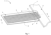
- Figure 1 shows an embodiment of the printed circuit 1 according to the invention, the printed circuit 1 comprising a base substrate 4 and a functional layer comprising a plurality of conductive tracks 5.
- the functional layer is arranged on the base substrate 4.
- the base substrate 4 and the functional layer comprise a main area 2 and a connection area 3 which are separated by an imaginary dividing line 6, with the connection area 3 being a prolongation of the main area 2, said connection area 3 being configured to cooperate with an electrical connector, not shown in the drawings.
- the printed circuit 1 also comprises a protective layer 7 which covers the functional layer in the main area 2, such that said protective layer 7 does not cover the tracks 5 of the functional layer in the imaginary dividing line 6.
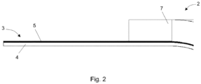
- the plurality of tracks 5 of the functional layer of the connection area 3 is not covered by the protective layer 7, as can be seen in Figure 2 , such that the tracks 5 of the connection area 3 are exposed. Furthermore, since the protective layer 7 does not cover the tracks 5 in the imaginary dividing line 6, if the connection area 3 is bent, for example during the handling of the printed circuit 1 for the final assembly thereof, for the packaging thereof, or for connecting the connection area 3 to the connector, on one hand, friction of the tracks 5 against the edge of the protective layer 7 is prevented when the connection area 3 is bent towards the protective layer 7, and on the other hand the tracks 5 are prevented from peeling off when the connection area 3 is bent in the opposite direction, preventing the deterioration of the tracks 5, as will be described in detail below.
- the protective layer 7 covers the functional layer in the entire main area 2 except in the segment of the imaginary dividing line 6 which is traversed by the tracks 5 and in an area 10 close to said segment, as shown in Figure 1 . Moreover, the protective layer 7 also covers the base substrate 4 in the entire main area 2 and at the ends 8 of the imaginary dividing line 6, but not in the area 10 close to the segment of the imaginary dividing line 6 which is traversed by the tracks 5, nor in the segment of the imaginary dividing line covering the tracks 5 intercalated with the base substrate 4.
- the edge of the protective layer 7 comprises a segment 9 parallel to the imaginary dividing line 6 facing the segment of the imaginary dividing line 6 traversed by the tracks 5, said segment 9 being joined to the rest of the edge of the protective layer 7 by means of curved segments, generating a type of empty space in the protective layer 7 close to the imaginary dividing line 6.
- the edge of the protective layer 7 covering the ends 8 of the imaginary dividing line 6 becomes an imaginary pivoting axis about which the connection area 3 can pivot or bend with respect to the main area 2 or vice versa.
- the printed circuit 1 is manufactured with the technology referred to as plastronics, commonly known as In-Mold Electronics (IME).
- IME In-Mold Electronics
- the IME technology consists of printing or screen printing on a substrate (foil), preferably flexible, using special inks both the esthetic part of the product and the electronics or functional part.
- the product is encapsulated by over-injecting a plastic which protects and covers both the substrate and the functional layer.
- the part modeled during thermoforming so that it adopts the three-dimensional final product shape is the main area 2.
- the base substrate 4 is flexible at the start of the process, the base substrate 4 of the main area 2 can become rigid after the thermoforming process, but the base substrate 4 of the connection area 3 remains flexible, such that there is a risk of the connection area 3 bending towards the protective layer 7 and/or in the opposite direction when handling the connection area 3, for example during the final assembly of the printed circuit 1, during the packaging of the printed circuit 1, or during the connection of the connection area 3 to the connector.
- connection area 3 is the imaginary dividing line 6 since the edge of the protective layer 7 covering the ends 8 of the imaginary dividing line 6 becomes the imaginary pivoting axis, where the connection area 3 can bend with respect to the main area 2.
- connection area 3 is flat, i.e., without reliefs, but optionally the connection area 3 may comprise at least one segment with a three-dimensional configuration, for example, a corrugated configuration, but such that said connection area 3 remains flexible, where it can be bent, as described in detail above.
- the edge of the protective layer 7 comprises a profile which, in the segment of the imaginary dividing line 6 which is traversed by the tracks 5, is arranged away from the imaginary dividing line 6 and therefore, if the connection area 3 is bent towards the protective layer 7, the tracks 5 do not contact the edge of the protective layer 7 and therefore do not rub against the protective layer 7, and if the connection area 3 is bent in the opposite direction, the tracks 5 do not come off (peel off) the base substrate 4, preventing the deterioration of the track 5 and therefore reducing the risk of generating defective products.
- the functional layer of the printed circuit 1 of the invention may also comprise electronic components such as, for example, a capacitor, a sensor, a resistor, or even a light source, preferably a base with light emitting diodes or LEDs, and even an element acting as a light diffuser.
- electronic components such as, for example, a capacitor, a sensor, a resistor, or even a light source, preferably a base with light emitting diodes or LEDs, and even an element acting as a light diffuser.
- the protective layer 7 is overmolded on the base substrate 4 and the functional layer of the main area 2, encapsulating the functional layer, even if it comprises electronic components.
- the protective layer 7 therefore protects the functional layer of the printed circuit 1.
- the protective layer 7 is made of plastic, preferably formed by a polymer material such as, for example, polycarbonate, being preferably transparent, and more preferably a good visible light transmitter.
- the material of the protective layer 7 may comprise additives, formulations, or surface treatments (such as paint, for example), which help to improve its light diffusion properties, for example, may also be applied as well.
- the protective layer 7 solidifies, and therefore becomes rigid, creating an edge in the contour of the protective layer 7, i.e., creating the outer contour of the protective layer 7.
- the tracks 5 of the functional layer which are preferably made of silver, may flake off if they rub against the edge of the protective layer 7, or peel off if the connection area 3 is bent away from the protective layer 7, hence the object of the invention is to arrange the edge of the protective layer 7 away from the imaginary dividing line 6, but such that the imaginary pivoting axis of the connection area 3 coincides with the imaginary dividing line 6.
- this layer can be rigid or flexible, depending on the material used.
- the main area 2 is more rigid than the connection area 3, not only due to the thermoforming process of the base substrate 4, but also to the protective layer 7. After the thermoforming process, the base substrate 4 of the main area 2 does not have to become rigid, but upon encapsulating same with the protective layer 7, the main area 2 usually ends up becoming rigid with the desired final shape.
- the tracks 5 of the functional layer are printed on the base substrate 4.
- Different printing techniques such as, for example, screen printing, flexography, ink injection, rotogravure printing, or offset printing can be used.
- the base substrate 4 is made of plastic, preferably polycarbonate, although other plastics are not ruled out.
- the base substrate 4 may also be, for example, a fabric.
- the material of the base substrate 4 may optionally comprise additives or can be formulated such that they improve its properties, for example, scratch resistance or the ultraviolet (UV) ray protection.
- the printed circuit of the invention may also comprise a non-functional layer, for example, a decorative layer, arranged on the base substrate 4 in the main area 2 and also encapsulated by the protective layer 7, and/or in the connection area 3 (not encapsulated by the protective layer 7).
- the functional layer can be arranged on the non-functional layer.
- the functional layer differs from the non-functional layer in that the functional layer contributes to the correct electrical operation of the printed circuit 1, i.e., the functional layer comprises the elements required for the printed circuit 1 to work.
- the base substrate 4 of the preferred embodiment is transparent, such that a non-functional layer has been applied on the base substrate 4 to change the appearance of the base substrate 4 before applying the functional layer.
- the base substrate 4 acquires a black color as a result of the non-functional layer which, in this case, is a decorative layer, although the decorative layer may have any other color or texture.
- connection area 3 is configured to be connected to a terminal, not shown in the figures, which may be connected to the electrical connector, not shown in the figures, to allow the electrical connection of the printed circuit 1 to a control unit, not shown in the drawings, said control unit comprising a power supply or electrical outlet, said control unit being configured to manage the printed circuit 1 of the invention.
Landscapes
- Engineering & Computer Science (AREA)
- Microelectronics & Electronic Packaging (AREA)
- Manufacturing & Machinery (AREA)
- Structure Of Printed Boards (AREA)
- Non-Metallic Protective Coatings For Printed Circuits (AREA)
Priority Applications (1)
| Application Number | Priority Date | Filing Date | Title |
|---|---|---|---|
| EP23382048.9A EP4404696A1 (de) | 2023-01-20 | 2023-01-20 | Leiterplatte |
Applications Claiming Priority (1)
| Application Number | Priority Date | Filing Date | Title |
|---|---|---|---|
| EP23382048.9A EP4404696A1 (de) | 2023-01-20 | 2023-01-20 | Leiterplatte |
Publications (1)
| Publication Number | Publication Date |
|---|---|
| EP4404696A1 true EP4404696A1 (de) | 2024-07-24 |
Family
ID=85227171
Family Applications (1)
| Application Number | Title | Priority Date | Filing Date |
|---|---|---|---|
| EP23382048.9A Withdrawn EP4404696A1 (de) | 2023-01-20 | 2023-01-20 | Leiterplatte |
Country Status (1)
| Country | Link |
|---|---|
| EP (1) | EP4404696A1 (de) |
Citations (5)
| Publication number | Priority date | Publication date | Assignee | Title |
|---|---|---|---|---|
| JP2003124583A (ja) | 2001-10-15 | 2003-04-25 | Alps Electric Co Ltd | フレキシブル基板 |
| KR20110086493A (ko) * | 2010-01-22 | 2011-07-28 | 이비덴 가부시키가이샤 | 플렉스 리지드 배선판 및 그의 제조 방법 |
| JP2012011691A (ja) * | 2010-07-01 | 2012-01-19 | Nissha Printing Co Ltd | 導電回路一体化成形品及びその製造方法 |
| US20150257265A1 (en) * | 2012-10-15 | 2015-09-10 | Polyic Gmbh & Co. Kg | Film and Boody with such a Film |
| US20180343741A1 (en) * | 2015-10-21 | 2018-11-29 | Adventive Ipbank | Method Of Fabricating 3D Bendable Printed Circuit Board |
-
2023
- 2023-01-20 EP EP23382048.9A patent/EP4404696A1/de not_active Withdrawn
Patent Citations (5)
| Publication number | Priority date | Publication date | Assignee | Title |
|---|---|---|---|---|
| JP2003124583A (ja) | 2001-10-15 | 2003-04-25 | Alps Electric Co Ltd | フレキシブル基板 |
| KR20110086493A (ko) * | 2010-01-22 | 2011-07-28 | 이비덴 가부시키가이샤 | 플렉스 리지드 배선판 및 그의 제조 방법 |
| JP2012011691A (ja) * | 2010-07-01 | 2012-01-19 | Nissha Printing Co Ltd | 導電回路一体化成形品及びその製造方法 |
| US20150257265A1 (en) * | 2012-10-15 | 2015-09-10 | Polyic Gmbh & Co. Kg | Film and Boody with such a Film |
| US20180343741A1 (en) * | 2015-10-21 | 2018-11-29 | Adventive Ipbank | Method Of Fabricating 3D Bendable Printed Circuit Board |
Similar Documents
| Publication | Publication Date | Title |
|---|---|---|
| EP3114910B1 (de) | Verfahren zur herstellung elektronischer produkte und entsprechende herstellungsanordnung | |
| JP6955529B2 (ja) | 電子機器用の多層の構造および関連製造方法 | |
| US9869810B2 (en) | Method for manufacturing electronic products, related arrangement and product | |
| KR102464287B1 (ko) | 전자 어셈블리의 제조 방법 및 전자 어셈블리 | |
| US12233630B2 (en) | In-mold electronic component and method for manufacturing the same | |
| US8475911B2 (en) | Device housing and manufacturing method for fabricating the same | |
| US10688916B2 (en) | Multiple resin over-mold for printed circuit board electronics and light guide | |
| CN118901286A (zh) | 用于制造数个电气节点的方法、电气节点模块、电气节点及多层结构 | |
| TWI907422B (zh) | 製造結構的方法及結構 | |
| US10939544B2 (en) | Multiple resin over-mold for printed circuit board electronics and light guide | |
| WO2007124280A3 (en) | Wiring board, production process thereof and connection method using same | |
| US12538438B2 (en) | Electronic device and method to produce electronic device | |
| CN113228834A (zh) | 在图形上多层电路的印刷 | |
| KR100463034B1 (ko) | 전자 제품용 커버 및 이의 제조 방법 | |
| JP2010228323A (ja) | プラスチックフィルムの印刷方法およびプラスチックフィルムと一体に成形された電子機器筐体 |
Legal Events
| Date | Code | Title | Description |
|---|---|---|---|
| PUAI | Public reference made under article 153(3) epc to a published international application that has entered the european phase |
Free format text: ORIGINAL CODE: 0009012 |
|
| STAA | Information on the status of an ep patent application or granted ep patent |
Free format text: STATUS: THE APPLICATION HAS BEEN PUBLISHED |
|
| AK | Designated contracting states |
Kind code of ref document: A1 Designated state(s): AL AT BE BG CH CY CZ DE DK EE ES FI FR GB GR HR HU IE IS IT LI LT LU LV MC ME MK MT NL NO PL PT RO RS SE SI SK SM TR |
|
| STAA | Information on the status of an ep patent application or granted ep patent |
Free format text: STATUS: REQUEST FOR EXAMINATION WAS MADE |
|
| 17P | Request for examination filed |
Effective date: 20240902 |
|
| RBV | Designated contracting states (corrected) |
Designated state(s): AL AT BE BG CH CY CZ DE DK EE ES FI FR GB GR HR HU IE IS IT LI LT LU LV MC ME MK MT NL NO PL PT RO RS SE SI SK SM TR |
|
| STAA | Information on the status of an ep patent application or granted ep patent |
Free format text: STATUS: THE APPLICATION IS DEEMED TO BE WITHDRAWN |
|
| 18D | Application deemed to be withdrawn |
Effective date: 20250801 |