EP2896499B1 - Verfahren zur herstellung eines produkts mit heller oberfläche - Google Patents
Verfahren zur herstellung eines produkts mit heller oberfläche Download PDFInfo
- Publication number
- EP2896499B1 EP2896499B1 EP13837443.4A EP13837443A EP2896499B1 EP 2896499 B1 EP2896499 B1 EP 2896499B1 EP 13837443 A EP13837443 A EP 13837443A EP 2896499 B1 EP2896499 B1 EP 2896499B1
- Authority
- EP
- European Patent Office
- Prior art keywords
- metal film
- substrate
- metal
- coat layer
- cracks
- Prior art date
- Legal status (The legal status is an assumption and is not a legal conclusion. Google has not performed a legal analysis and makes no representation as to the accuracy of the status listed.)
- Not-in-force
Links
Images


Classifications
-
- B—PERFORMING OPERATIONS; TRANSPORTING
- B32—LAYERED PRODUCTS
- B32B—LAYERED PRODUCTS, i.e. PRODUCTS BUILT-UP OF STRATA OF FLAT OR NON-FLAT, e.g. CELLULAR OR HONEYCOMB, FORM
- B32B33/00—Layered products characterised by particular properties or particular surface features, e.g. particular surface coatings; Layered products designed for particular purposes not covered by another single class
-
- C—CHEMISTRY; METALLURGY
- C23—COATING METALLIC MATERIAL; COATING MATERIAL WITH METALLIC MATERIAL; CHEMICAL SURFACE TREATMENT; DIFFUSION TREATMENT OF METALLIC MATERIAL; COATING BY VACUUM EVAPORATION, BY SPUTTERING, BY ION IMPLANTATION OR BY CHEMICAL VAPOUR DEPOSITION, IN GENERAL; INHIBITING CORROSION OF METALLIC MATERIAL OR INCRUSTATION IN GENERAL
- C23C—COATING METALLIC MATERIAL; COATING MATERIAL WITH METALLIC MATERIAL; SURFACE TREATMENT OF METALLIC MATERIAL BY DIFFUSION INTO THE SURFACE, BY CHEMICAL CONVERSION OR SUBSTITUTION; COATING BY VACUUM EVAPORATION, BY SPUTTERING, BY ION IMPLANTATION OR BY CHEMICAL VAPOUR DEPOSITION, IN GENERAL
- C23C18/00—Chemical coating by decomposition of either liquid compounds or solutions of the coating forming compounds, without leaving reaction products of surface material in the coating; Contact plating
- C23C18/16—Chemical coating by decomposition of either liquid compounds or solutions of the coating forming compounds, without leaving reaction products of surface material in the coating; Contact plating by reduction or substitution, e.g. electroless plating
- C23C18/1601—Process or apparatus
- C23C18/1633—Process of electroless plating
- C23C18/1646—Characteristics of the product obtained
- C23C18/165—Multilayered product
- C23C18/1653—Two or more layers with at least one layer obtained by electroless plating and one layer obtained by electroplating
-
- B—PERFORMING OPERATIONS; TRANSPORTING
- B32—LAYERED PRODUCTS
- B32B—LAYERED PRODUCTS, i.e. PRODUCTS BUILT-UP OF STRATA OF FLAT OR NON-FLAT, e.g. CELLULAR OR HONEYCOMB, FORM
- B32B15/00—Layered products comprising a layer of metal
- B32B15/04—Layered products comprising a layer of metal comprising metal as the main or only constituent of a layer, which is next to another layer of the same or of a different material
- B32B15/08—Layered products comprising a layer of metal comprising metal as the main or only constituent of a layer, which is next to another layer of the same or of a different material of synthetic resin
-
- B—PERFORMING OPERATIONS; TRANSPORTING
- B32—LAYERED PRODUCTS
- B32B—LAYERED PRODUCTS, i.e. PRODUCTS BUILT-UP OF STRATA OF FLAT OR NON-FLAT, e.g. CELLULAR OR HONEYCOMB, FORM
- B32B3/00—Layered products comprising a layer with external or internal discontinuities or unevennesses, or a layer of non-planar shape; Layered products comprising a layer having particular features of form
- B32B3/26—Layered products comprising a layer with external or internal discontinuities or unevennesses, or a layer of non-planar shape; Layered products comprising a layer having particular features of form characterised by a particular shape of the outline of the cross-section of a continuous layer; characterised by a layer with cavities or internal voids ; characterised by an apertured layer
- B32B3/266—Layered products comprising a layer with external or internal discontinuities or unevennesses, or a layer of non-planar shape; Layered products comprising a layer having particular features of form characterised by a particular shape of the outline of the cross-section of a continuous layer; characterised by a layer with cavities or internal voids ; characterised by an apertured layer characterised by an apertured layer, the apertures going through the whole thickness of the layer, e.g. expanded metal, perforated layer, slit layer regular cells B32B3/12
-
- B—PERFORMING OPERATIONS; TRANSPORTING
- B32—LAYERED PRODUCTS
- B32B—LAYERED PRODUCTS, i.e. PRODUCTS BUILT-UP OF STRATA OF FLAT OR NON-FLAT, e.g. CELLULAR OR HONEYCOMB, FORM
- B32B38/00—Ancillary operations in connection with laminating processes
- B32B38/0004—Cutting, tearing or severing, e.g. bursting; Cutter details
-
- B—PERFORMING OPERATIONS; TRANSPORTING
- B32—LAYERED PRODUCTS
- B32B—LAYERED PRODUCTS, i.e. PRODUCTS BUILT-UP OF STRATA OF FLAT OR NON-FLAT, e.g. CELLULAR OR HONEYCOMB, FORM
- B32B7/00—Layered products characterised by the relation between layers; Layered products characterised by the relative orientation of features between layers, or by the relative values of a measurable parameter between layers, i.e. products comprising layers having different physical, chemical or physicochemical properties; Layered products characterised by the interconnection of layers
- B32B7/04—Interconnection of layers
- B32B7/12—Interconnection of layers using interposed adhesives or interposed materials with bonding properties
-
- C—CHEMISTRY; METALLURGY
- C23—COATING METALLIC MATERIAL; COATING MATERIAL WITH METALLIC MATERIAL; CHEMICAL SURFACE TREATMENT; DIFFUSION TREATMENT OF METALLIC MATERIAL; COATING BY VACUUM EVAPORATION, BY SPUTTERING, BY ION IMPLANTATION OR BY CHEMICAL VAPOUR DEPOSITION, IN GENERAL; INHIBITING CORROSION OF METALLIC MATERIAL OR INCRUSTATION IN GENERAL
- C23C—COATING METALLIC MATERIAL; COATING MATERIAL WITH METALLIC MATERIAL; SURFACE TREATMENT OF METALLIC MATERIAL BY DIFFUSION INTO THE SURFACE, BY CHEMICAL CONVERSION OR SUBSTITUTION; COATING BY VACUUM EVAPORATION, BY SPUTTERING, BY ION IMPLANTATION OR BY CHEMICAL VAPOUR DEPOSITION, IN GENERAL
- C23C18/00—Chemical coating by decomposition of either liquid compounds or solutions of the coating forming compounds, without leaving reaction products of surface material in the coating; Contact plating
- C23C18/16—Chemical coating by decomposition of either liquid compounds or solutions of the coating forming compounds, without leaving reaction products of surface material in the coating; Contact plating by reduction or substitution, e.g. electroless plating
- C23C18/1601—Process or apparatus
- C23C18/1633—Process of electroless plating
- C23C18/1635—Composition of the substrate
- C23C18/1639—Substrates other than metallic, e.g. inorganic or organic or non-conductive
- C23C18/1641—Organic substrates, e.g. resin, plastic
-
- C—CHEMISTRY; METALLURGY
- C23—COATING METALLIC MATERIAL; COATING MATERIAL WITH METALLIC MATERIAL; CHEMICAL SURFACE TREATMENT; DIFFUSION TREATMENT OF METALLIC MATERIAL; COATING BY VACUUM EVAPORATION, BY SPUTTERING, BY ION IMPLANTATION OR BY CHEMICAL VAPOUR DEPOSITION, IN GENERAL; INHIBITING CORROSION OF METALLIC MATERIAL OR INCRUSTATION IN GENERAL
- C23C—COATING METALLIC MATERIAL; COATING MATERIAL WITH METALLIC MATERIAL; SURFACE TREATMENT OF METALLIC MATERIAL BY DIFFUSION INTO THE SURFACE, BY CHEMICAL CONVERSION OR SUBSTITUTION; COATING BY VACUUM EVAPORATION, BY SPUTTERING, BY ION IMPLANTATION OR BY CHEMICAL VAPOUR DEPOSITION, IN GENERAL
- C23C18/00—Chemical coating by decomposition of either liquid compounds or solutions of the coating forming compounds, without leaving reaction products of surface material in the coating; Contact plating
- C23C18/16—Chemical coating by decomposition of either liquid compounds or solutions of the coating forming compounds, without leaving reaction products of surface material in the coating; Contact plating by reduction or substitution, e.g. electroless plating
- C23C18/1601—Process or apparatus
- C23C18/1633—Process of electroless plating
- C23C18/1646—Characteristics of the product obtained
- C23C18/165—Multilayered product
-
- C—CHEMISTRY; METALLURGY
- C23—COATING METALLIC MATERIAL; COATING MATERIAL WITH METALLIC MATERIAL; CHEMICAL SURFACE TREATMENT; DIFFUSION TREATMENT OF METALLIC MATERIAL; COATING BY VACUUM EVAPORATION, BY SPUTTERING, BY ION IMPLANTATION OR BY CHEMICAL VAPOUR DEPOSITION, IN GENERAL; INHIBITING CORROSION OF METALLIC MATERIAL OR INCRUSTATION IN GENERAL
- C23C—COATING METALLIC MATERIAL; COATING MATERIAL WITH METALLIC MATERIAL; SURFACE TREATMENT OF METALLIC MATERIAL BY DIFFUSION INTO THE SURFACE, BY CHEMICAL CONVERSION OR SUBSTITUTION; COATING BY VACUUM EVAPORATION, BY SPUTTERING, BY ION IMPLANTATION OR BY CHEMICAL VAPOUR DEPOSITION, IN GENERAL
- C23C18/00—Chemical coating by decomposition of either liquid compounds or solutions of the coating forming compounds, without leaving reaction products of surface material in the coating; Contact plating
- C23C18/16—Chemical coating by decomposition of either liquid compounds or solutions of the coating forming compounds, without leaving reaction products of surface material in the coating; Contact plating by reduction or substitution, e.g. electroless plating
- C23C18/1601—Process or apparatus
- C23C18/1633—Process of electroless plating
- C23C18/1689—After-treatment
- C23C18/1692—Heat-treatment
-
- C—CHEMISTRY; METALLURGY
- C25—ELECTROLYTIC OR ELECTROPHORETIC PROCESSES; APPARATUS THEREFOR
- C25D—PROCESSES FOR THE ELECTROLYTIC OR ELECTROPHORETIC PRODUCTION OF COATINGS; ELECTROFORMING; APPARATUS THEREFOR
- C25D5/00—Electroplating characterised by the process; Pretreatment or after-treatment of workpieces
- C25D5/10—Electroplating with more than one layer of the same or of different metals
- C25D5/12—Electroplating with more than one layer of the same or of different metals at least one layer being of nickel or chromium
-
- C—CHEMISTRY; METALLURGY
- C25—ELECTROLYTIC OR ELECTROPHORETIC PROCESSES; APPARATUS THEREFOR
- C25D—PROCESSES FOR THE ELECTROLYTIC OR ELECTROPHORETIC PRODUCTION OF COATINGS; ELECTROFORMING; APPARATUS THEREFOR
- C25D5/00—Electroplating characterised by the process; Pretreatment or after-treatment of workpieces
- C25D5/48—After-treatment of electroplated surfaces
- C25D5/50—After-treatment of electroplated surfaces by heat-treatment
-
- C—CHEMISTRY; METALLURGY
- C25—ELECTROLYTIC OR ELECTROPHORETIC PROCESSES; APPARATUS THEREFOR
- C25D—PROCESSES FOR THE ELECTROLYTIC OR ELECTROPHORETIC PRODUCTION OF COATINGS; ELECTROFORMING; APPARATUS THEREFOR
- C25D5/00—Electroplating characterised by the process; Pretreatment or after-treatment of workpieces
- C25D5/48—After-treatment of electroplated surfaces
- C25D5/50—After-treatment of electroplated surfaces by heat-treatment
- C25D5/505—After-treatment of electroplated surfaces by heat-treatment of electroplated tin coatings, e.g. by melting
-
- C—CHEMISTRY; METALLURGY
- C25—ELECTROLYTIC OR ELECTROPHORETIC PROCESSES; APPARATUS THEREFOR
- C25D—PROCESSES FOR THE ELECTROLYTIC OR ELECTROPHORETIC PRODUCTION OF COATINGS; ELECTROFORMING; APPARATUS THEREFOR
- C25D5/00—Electroplating characterised by the process; Pretreatment or after-treatment of workpieces
- C25D5/60—Electroplating characterised by the structure or texture of the layers
- C25D5/625—Discontinuous layers, e.g. microcracked layers
-
- C—CHEMISTRY; METALLURGY
- C25—ELECTROLYTIC OR ELECTROPHORETIC PROCESSES; APPARATUS THEREFOR
- C25D—PROCESSES FOR THE ELECTROLYTIC OR ELECTROPHORETIC PRODUCTION OF COATINGS; ELECTROFORMING; APPARATUS THEREFOR
- C25D5/00—Electroplating characterised by the process; Pretreatment or after-treatment of workpieces
- C25D5/627—Electroplating characterised by the visual appearance of the layers, e.g. colour, brightness or mat appearance
-
- C—CHEMISTRY; METALLURGY
- C25—ELECTROLYTIC OR ELECTROPHORETIC PROCESSES; APPARATUS THEREFOR
- C25D—PROCESSES FOR THE ELECTROLYTIC OR ELECTROPHORETIC PRODUCTION OF COATINGS; ELECTROFORMING; APPARATUS THEREFOR
- C25D7/00—Electroplating characterised by the article coated
-
- B—PERFORMING OPERATIONS; TRANSPORTING
- B32—LAYERED PRODUCTS
- B32B—LAYERED PRODUCTS, i.e. PRODUCTS BUILT-UP OF STRATA OF FLAT OR NON-FLAT, e.g. CELLULAR OR HONEYCOMB, FORM
- B32B2307/00—Properties of the layers or laminate
- B32B2307/40—Properties of the layers or laminate having particular optical properties
- B32B2307/406—Bright, glossy, shiny surface
-
- B—PERFORMING OPERATIONS; TRANSPORTING
- B32—LAYERED PRODUCTS
- B32B—LAYERED PRODUCTS, i.e. PRODUCTS BUILT-UP OF STRATA OF FLAT OR NON-FLAT, e.g. CELLULAR OR HONEYCOMB, FORM
- B32B2307/00—Properties of the layers or laminate
- B32B2307/70—Other properties
- B32B2307/714—Inert, i.e. inert to chemical degradation, corrosion
-
- B—PERFORMING OPERATIONS; TRANSPORTING
- B32—LAYERED PRODUCTS
- B32B—LAYERED PRODUCTS, i.e. PRODUCTS BUILT-UP OF STRATA OF FLAT OR NON-FLAT, e.g. CELLULAR OR HONEYCOMB, FORM
- B32B2605/00—Vehicles
- B32B2605/08—Cars
-
- C—CHEMISTRY; METALLURGY
- C23—COATING METALLIC MATERIAL; COATING MATERIAL WITH METALLIC MATERIAL; CHEMICAL SURFACE TREATMENT; DIFFUSION TREATMENT OF METALLIC MATERIAL; COATING BY VACUUM EVAPORATION, BY SPUTTERING, BY ION IMPLANTATION OR BY CHEMICAL VAPOUR DEPOSITION, IN GENERAL; INHIBITING CORROSION OF METALLIC MATERIAL OR INCRUSTATION IN GENERAL
- C23C—COATING METALLIC MATERIAL; COATING MATERIAL WITH METALLIC MATERIAL; SURFACE TREATMENT OF METALLIC MATERIAL BY DIFFUSION INTO THE SURFACE, BY CHEMICAL CONVERSION OR SUBSTITUTION; COATING BY VACUUM EVAPORATION, BY SPUTTERING, BY ION IMPLANTATION OR BY CHEMICAL VAPOUR DEPOSITION, IN GENERAL
- C23C18/00—Chemical coating by decomposition of either liquid compounds or solutions of the coating forming compounds, without leaving reaction products of surface material in the coating; Contact plating
- C23C18/16—Chemical coating by decomposition of either liquid compounds or solutions of the coating forming compounds, without leaving reaction products of surface material in the coating; Contact plating by reduction or substitution, e.g. electroless plating
- C23C18/18—Pretreatment of the material to be coated
- C23C18/20—Pretreatment of the material to be coated of organic surfaces, e.g. resins
- C23C18/2006—Pretreatment of the material to be coated of organic surfaces, e.g. resins by other methods than those of C23C18/22 - C23C18/30
- C23C18/2026—Pretreatment of the material to be coated of organic surfaces, e.g. resins by other methods than those of C23C18/22 - C23C18/30 by radiant energy
- C23C18/204—Radiation, e.g. UV, laser
-
- C—CHEMISTRY; METALLURGY
- C23—COATING METALLIC MATERIAL; COATING MATERIAL WITH METALLIC MATERIAL; CHEMICAL SURFACE TREATMENT; DIFFUSION TREATMENT OF METALLIC MATERIAL; COATING BY VACUUM EVAPORATION, BY SPUTTERING, BY ION IMPLANTATION OR BY CHEMICAL VAPOUR DEPOSITION, IN GENERAL; INHIBITING CORROSION OF METALLIC MATERIAL OR INCRUSTATION IN GENERAL
- C23C—COATING METALLIC MATERIAL; COATING MATERIAL WITH METALLIC MATERIAL; SURFACE TREATMENT OF METALLIC MATERIAL BY DIFFUSION INTO THE SURFACE, BY CHEMICAL CONVERSION OR SUBSTITUTION; COATING BY VACUUM EVAPORATION, BY SPUTTERING, BY ION IMPLANTATION OR BY CHEMICAL VAPOUR DEPOSITION, IN GENERAL
- C23C18/00—Chemical coating by decomposition of either liquid compounds or solutions of the coating forming compounds, without leaving reaction products of surface material in the coating; Contact plating
- C23C18/16—Chemical coating by decomposition of either liquid compounds or solutions of the coating forming compounds, without leaving reaction products of surface material in the coating; Contact plating by reduction or substitution, e.g. electroless plating
- C23C18/18—Pretreatment of the material to be coated
- C23C18/20—Pretreatment of the material to be coated of organic surfaces, e.g. resins
- C23C18/2006—Pretreatment of the material to be coated of organic surfaces, e.g. resins by other methods than those of C23C18/22 - C23C18/30
- C23C18/2046—Pretreatment of the material to be coated of organic surfaces, e.g. resins by other methods than those of C23C18/22 - C23C18/30 by chemical pretreatment
- C23C18/2073—Multistep pretreatment
- C23C18/2086—Multistep pretreatment with use of organic or inorganic compounds other than metals, first
-
- C—CHEMISTRY; METALLURGY
- C23—COATING METALLIC MATERIAL; COATING MATERIAL WITH METALLIC MATERIAL; CHEMICAL SURFACE TREATMENT; DIFFUSION TREATMENT OF METALLIC MATERIAL; COATING BY VACUUM EVAPORATION, BY SPUTTERING, BY ION IMPLANTATION OR BY CHEMICAL VAPOUR DEPOSITION, IN GENERAL; INHIBITING CORROSION OF METALLIC MATERIAL OR INCRUSTATION IN GENERAL
- C23C—COATING METALLIC MATERIAL; COATING MATERIAL WITH METALLIC MATERIAL; SURFACE TREATMENT OF METALLIC MATERIAL BY DIFFUSION INTO THE SURFACE, BY CHEMICAL CONVERSION OR SUBSTITUTION; COATING BY VACUUM EVAPORATION, BY SPUTTERING, BY ION IMPLANTATION OR BY CHEMICAL VAPOUR DEPOSITION, IN GENERAL
- C23C18/00—Chemical coating by decomposition of either liquid compounds or solutions of the coating forming compounds, without leaving reaction products of surface material in the coating; Contact plating
- C23C18/16—Chemical coating by decomposition of either liquid compounds or solutions of the coating forming compounds, without leaving reaction products of surface material in the coating; Contact plating by reduction or substitution, e.g. electroless plating
- C23C18/18—Pretreatment of the material to be coated
- C23C18/20—Pretreatment of the material to be coated of organic surfaces, e.g. resins
- C23C18/28—Sensitising or activating
- C23C18/285—Sensitising or activating with tin based compound or composition
-
- C—CHEMISTRY; METALLURGY
- C23—COATING METALLIC MATERIAL; COATING MATERIAL WITH METALLIC MATERIAL; CHEMICAL SURFACE TREATMENT; DIFFUSION TREATMENT OF METALLIC MATERIAL; COATING BY VACUUM EVAPORATION, BY SPUTTERING, BY ION IMPLANTATION OR BY CHEMICAL VAPOUR DEPOSITION, IN GENERAL; INHIBITING CORROSION OF METALLIC MATERIAL OR INCRUSTATION IN GENERAL
- C23C—COATING METALLIC MATERIAL; COATING MATERIAL WITH METALLIC MATERIAL; SURFACE TREATMENT OF METALLIC MATERIAL BY DIFFUSION INTO THE SURFACE, BY CHEMICAL CONVERSION OR SUBSTITUTION; COATING BY VACUUM EVAPORATION, BY SPUTTERING, BY ION IMPLANTATION OR BY CHEMICAL VAPOUR DEPOSITION, IN GENERAL
- C23C18/00—Chemical coating by decomposition of either liquid compounds or solutions of the coating forming compounds, without leaving reaction products of surface material in the coating; Contact plating
- C23C18/16—Chemical coating by decomposition of either liquid compounds or solutions of the coating forming compounds, without leaving reaction products of surface material in the coating; Contact plating by reduction or substitution, e.g. electroless plating
- C23C18/18—Pretreatment of the material to be coated
- C23C18/20—Pretreatment of the material to be coated of organic surfaces, e.g. resins
- C23C18/28—Sensitising or activating
- C23C18/30—Activating or accelerating or sensitising with palladium or other noble metal
-
- C—CHEMISTRY; METALLURGY
- C23—COATING METALLIC MATERIAL; COATING MATERIAL WITH METALLIC MATERIAL; CHEMICAL SURFACE TREATMENT; DIFFUSION TREATMENT OF METALLIC MATERIAL; COATING BY VACUUM EVAPORATION, BY SPUTTERING, BY ION IMPLANTATION OR BY CHEMICAL VAPOUR DEPOSITION, IN GENERAL; INHIBITING CORROSION OF METALLIC MATERIAL OR INCRUSTATION IN GENERAL
- C23C—COATING METALLIC MATERIAL; COATING MATERIAL WITH METALLIC MATERIAL; SURFACE TREATMENT OF METALLIC MATERIAL BY DIFFUSION INTO THE SURFACE, BY CHEMICAL CONVERSION OR SUBSTITUTION; COATING BY VACUUM EVAPORATION, BY SPUTTERING, BY ION IMPLANTATION OR BY CHEMICAL VAPOUR DEPOSITION, IN GENERAL
- C23C18/00—Chemical coating by decomposition of either liquid compounds or solutions of the coating forming compounds, without leaving reaction products of surface material in the coating; Contact plating
- C23C18/16—Chemical coating by decomposition of either liquid compounds or solutions of the coating forming compounds, without leaving reaction products of surface material in the coating; Contact plating by reduction or substitution, e.g. electroless plating
- C23C18/31—Coating with metals
- C23C18/32—Coating with nickel, cobalt or mixtures thereof with phosphorus or boron
-
- C—CHEMISTRY; METALLURGY
- C23—COATING METALLIC MATERIAL; COATING MATERIAL WITH METALLIC MATERIAL; CHEMICAL SURFACE TREATMENT; DIFFUSION TREATMENT OF METALLIC MATERIAL; COATING BY VACUUM EVAPORATION, BY SPUTTERING, BY ION IMPLANTATION OR BY CHEMICAL VAPOUR DEPOSITION, IN GENERAL; INHIBITING CORROSION OF METALLIC MATERIAL OR INCRUSTATION IN GENERAL
- C23C—COATING METALLIC MATERIAL; COATING MATERIAL WITH METALLIC MATERIAL; SURFACE TREATMENT OF METALLIC MATERIAL BY DIFFUSION INTO THE SURFACE, BY CHEMICAL CONVERSION OR SUBSTITUTION; COATING BY VACUUM EVAPORATION, BY SPUTTERING, BY ION IMPLANTATION OR BY CHEMICAL VAPOUR DEPOSITION, IN GENERAL
- C23C18/00—Chemical coating by decomposition of either liquid compounds or solutions of the coating forming compounds, without leaving reaction products of surface material in the coating; Contact plating
- C23C18/16—Chemical coating by decomposition of either liquid compounds or solutions of the coating forming compounds, without leaving reaction products of surface material in the coating; Contact plating by reduction or substitution, e.g. electroless plating
- C23C18/48—Coating with alloys
-
- C—CHEMISTRY; METALLURGY
- C25—ELECTROLYTIC OR ELECTROPHORETIC PROCESSES; APPARATUS THEREFOR
- C25D—PROCESSES FOR THE ELECTROLYTIC OR ELECTROPHORETIC PRODUCTION OF COATINGS; ELECTROFORMING; APPARATUS THEREFOR
- C25D3/00—Electroplating: Baths therefor
- C25D3/02—Electroplating: Baths therefor from solutions
- C25D3/04—Electroplating: Baths therefor from solutions of chromium
-
- C—CHEMISTRY; METALLURGY
- C25—ELECTROLYTIC OR ELECTROPHORETIC PROCESSES; APPARATUS THEREFOR
- C25D—PROCESSES FOR THE ELECTROLYTIC OR ELECTROPHORETIC PRODUCTION OF COATINGS; ELECTROFORMING; APPARATUS THEREFOR
- C25D3/00—Electroplating: Baths therefor
- C25D3/02—Electroplating: Baths therefor from solutions
- C25D3/38—Electroplating: Baths therefor from solutions of copper
Definitions
- the diversification of the texture of surface brightness, the properties of an island-like metal film and applicable bright surface products can be further achieved by configuring fine multi-layered metal regions comprising an electroless plating metal layer and two electrolytic plating metal layers.
- the bonding strength between each film of a multi-layered metal film can be enhanced by utilizing the bonding strength between a substrate or a base coat layer and a first metal layer thereon, and the difference in internal stress can be allowed to easily arise to more simply and reliably perform the formation of cracks in the multi-layered metal film formed on the substrate or the base coat layer.
- the difference in internal stress can be allowed to easily arise to more simply and reliably perform the formation of cracks in the metal film formed on the substrate or the base coat layer.
- island-like metal films of these various metals or island-like metal films having these various metals in an underlying layer can be obtained, and the properties of these various metals can be effectively used.
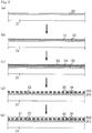
- the metal film 13 is discontinuously segmentalized with the cracks 15 to form an island-like metal film comprising a collection of the fine metal regions 14 with island-like structures and having an appearance of an integrated bright surface.
- This segmentalization of the metal film 13 due to the difference in internal stress may be due to, for example, the difference in internal stress between the substrate 11 and the metal film 13 which is produced during a heat treatment at 80°C or more and the like, or the difference in internal stress between the substrate 11 and the metal film 13 which remains in a state where they are removed from an electroless plating bath.
- a bright surface product having good surface brightness can be obtained by forming an island-like metal film having an appearance of an integrated bright surface. Further, an island-like metal film is formed with the fine metal regions 14 so that the top coat layer 16 covers the fine metal regions 14 and enters into the cracks 15 to make contact with the base coat layer 12 and the substrate 11. Therefore, the formation and expansion of crevices when external force is applied can be prevented to eliminate the possibility of an extraordinary dangerous situation against a human body, and in addition the adherence of the top coat layer 16 can be improved to obtain a bright surface product having excellent rust and detachment resistance.
- the substrate 21 and the base coat layer 22 provided on the substrate 21 if desired are fundamentally the same as the substrate 11 and the base coat layer 12 according to the first embodiment.
- the island-like metal film comprising a collection of the fine multi-layered metal regions 25 with island-like structures is directly formed on the substrate 21, and the top coat layer 27 with translucency described below is formed to cover the fine multi-layered metal regions 25 of the island-like metal film and enter into the cracks 26 to make contact with the substrate 21.
- the mean maximum width (the longest distance between edges when a distance from one edge to the other of the fine multi-layered metal region 25 to be measured, or a diameter obtained by computing a diameter of a circle having the same area as the fine multi-layered metal region 25 by using an image processing system and the like) is, for example, around 20 ⁇ m. Further, in a case where the width of the crack 26 is too small, the entrance and adhesion of the top coat layer 27 into and on the crack 26 is difficult to be achieved. In a case where it is too large, the appearance of an integrated bright surface is difficult to be achieved. Therefore, the width is preferably 10 nm to 2 ⁇ m, more preferably 30 nm to 500 nm.
- the base coat layer 22 is deposited on the substrate 21 if desired, and electroless plating is performed to form the first metal film 23 as a continuous film on the base coat layer 22 deposited on the substrate 21 or the substrate 21.
- Procedures for formation of the base coat layer 22 and formation of the first metal film 23 are similar to those for formation of the base coat layer 12 and formation of the metal film 13 according to the first embodiment.
- the substrate 21 is of a synthetic resin
- an ultraviolet irradiation may be performed on the surface of the substrate 21 under the atmosphere to form a modified layer on the surface, and the first metal film 23 may be formed thereon by electroless plating.
- the substrate 31 and the base coat layer 32 provided on the substrate 31 if desired are fundamentally the same as the substrates 11, 21 and the base coat layers 12, 22 according to the first and second embodiments.
- an island-like metal film comprising a collection of the fine multi-layered metal regions 36 with island-like structures may be directly formed on the substrate 31, and the top coat layer 38 with translucency described below is formed to cover the fine multi-layered metal regions 36 of the island-like metal film and enter into the cracks 37 to make contact with the substrate 31.
- the mean maximum width of the fine multi-layered metal regions 36 is, for example, around 5 ⁇ m.
- the width of the crack 37 is preferably 10 nm to 2 ⁇ m, more preferably 30 nm to 500 nm.
- the top coat layer 38 with translucency is formed to cover the fine multi-layered metal regions 36 of the island-like metal film and enter into the cracks 37 to make contact with the base coat layer 32 or the substrate 31.
- the top coat layer 38 is formed with, for example, silicone acrylic resin, acryl urethane resin, urethane resin and the like.
- the thickness of the base coat layer 32 is thinner by an order of magnitude than that of the substrate 31, the influence from the internal stress in the base coat layer 32 is small, and thus, the multi-layered metal film will be segmentalized with the cracks 37 due to the difference in internal stress between the substrate 31 and the metal films 33, 34, 35 or the first metal film 33.
- the following anti-chipping test was conducted for the test sample.
- the anti-chipping performance was measured with a gravelometer.
- the coating surface was mounted in a specified direction, and a chipping test was performed with standard stones (Macadam No. 6) at an ejection air pressure of 0.392 ⁇ 0.019 MPa, an air flow rate of 40 to 50 L/sec, a total amount used of 500 ⁇ 10 g and at room temperature.
- the sample after the test was removed, and stone wastes, dusts and the like on the coating surface were removed, and then a salt water spray test was performed for 80 hours.
- the test piece was removed after the salt water spray test, and the coating surface was washed with clean running water, and left to stand for 2 hours, and then an adhesive tape was adhered on the front side of the coating film to perform an adhesion test.
- As the adhesive tape a Nichiban adhesive cellophane tape was used. The adhesive cellophane tape was adhered so that air bubbles were not left on the coating surface. Next, the tape was lifted at one end of the adhesive cellophane tape with the hand so that the angle between the adhesive cellophane tape and the test surface became about 45 degrees. Then the tape was rapidly pulled in that direction to peel the test piece off. Peel evaluations were classified using the evaluation table shown in Table 1. As a result, the best evaluation A was obtained.
- Example 2 corresponds to the first embodiment.
- ABS resin MTH2, Japan A&L Inc. Size: 130 mm x 80 mm x 3 mm; thermal expansion coefficient: 60 x 10 -6 /°C
- a coating liquid in which an acrylic resin (UTU570: Toho Kaken Manufacturing Inc.) was diluted with a solvent was spray-coated on one side of the ABS resin material, and then UV curing was performed to form a base coat layer having a thickness of 20 ⁇ m as an organic coating film.
- the substrate was immersed in a 10% sulfuric acid aqueous solution for 1 minute under a condition of 45°C
- the substrate in which a palladium metal as a catalyst has been adsorbed in the base coat layer was immersed for 40 seconds in an electroless palladium-phosphorus alloy plating bath having the following bath composition adjusted at 40°C to deposit a metal film of the palladium-phosphorus alloy on the surface of the base coat layer.
- a network of cracks was formed when the ratio of the thermal expansion coefficients of the substrate and the metal plating film was 3 times or more. Subsequently, spray coating was performed such that an acrylic silicone-urethane based thermoset clear coating (R227HF) has a film thickness of 20 ⁇ m or more, and baking was performed at 80°C for 1 hour, and then allowed to stand for 72 hours or more at room temperature to obtain a test sample.
- R227HF acrylic silicone-urethane based thermoset clear coating
- Example 3 corresponds to the second embodiment.
- ABS resin MTH2, Japan A&L Inc. Size: 130 mm x 80 mm x 3 mm; thermal expansion coefficient: 60 x 10 -6 /°C
- a coating liquid in which an acrylic resin (UTU570: Toho Kaken Manufacturing Inc.) was diluted with a solvent was spray-coated on one side of the ABS resin material, and then UV curing was performed to form a base coat layer having a thickness of 20 ⁇ m as an organic coating film.
- the thermal expansion coefficient of the ABS resin as a substrate: 60 x 10 -6 /°C is 3 times or more of the thermal expansion coefficient of nickel: 14 x 10 -6 /°C and the thermal expansion coefficient of chromium: 6 x 10 -6 /°C.
- a metal plating on a metal usually shows a strong bonding strength since free electrons flow between them. When thermal stress and the like is created, less force is required for breaking a bonding portion between a multi-layered metal film and a substrate or a base coat layer than for detaching a bonding area of a multi-layered metal film.
- the adhesion strength of the chromium plating on nickel in the present Example is strong.
- Example 1 As a result of performing a similar adhesion test as in Example 1 on this test sample, the number of squares in which 50% or more of the coating film was exfoliated in each square was 0. Further, as a result of performing a similar anti-chipping test as in Example 1 on this test sample, the best evaluation A was obtained.
Landscapes
- Chemical & Material Sciences (AREA)
- Engineering & Computer Science (AREA)
- Chemical Kinetics & Catalysis (AREA)
- Materials Engineering (AREA)
- Metallurgy (AREA)
- Organic Chemistry (AREA)
- Electrochemistry (AREA)
- Mechanical Engineering (AREA)
- General Chemical & Material Sciences (AREA)
- Inorganic Chemistry (AREA)
- Laminated Bodies (AREA)
- Chemically Coating (AREA)
Claims (5)
- Verfahren zur Herstellung eines Produkts mit heller Oberfläche als Kraftfahrzeugteil mit Belastungsbeständigkeit gegen externe Kollisionskräfte, wobei das Verfahren Folgendes beinhaltet:einen ersten Schritt des Durchführens von stromloser Abscheidung in einem stromlosen Abscheidungsbad zum Bilden eines Metallfilms (13), der Nickel oder eine Nickellegierung, Palladium oder eine Palladiumlegierung, Zinn oder eine Zinnlegierung, Kupfer oder eine Kupferlegierung, Silber oder eine Silberlegierung, Gold oder eine Goldlegierung oder Kobalt oder eine Kobaltlegierung umfasst, auf einem Substrat (11), das Harze, Metalle, Keramiken, Papier oder Glas umfasst, oder eine auf das Substrat (11) abgesetzte Grundierungsschicht (12);einen zweiten Schritt des Zulassens einer diskontinuierlichen Segmentalisierung des Metallfilms (13) mit Rissen (15) entweder:bei einer Wärmebehandlung bei 80°C oder mehr, um dadurch die Differenz an innerer Spannung zwischen dem Substrat (11) und dem Metallfilm (13) zu nutzen; odernach seiner Entfernung aus dem stromlosen Abscheidungsbad, um dadurch die in dem Metallfilm (13) zurückbleibende innere Spannung zu nutzen, wenn das Substrat (11) und der Metallfilm (13) aus dem stromlosen Abscheidungsbad entfernt und auf Raumtemperatur gekühlt wurde;zum Bilden eines inselähnlichen Metallfilms, der eine Kollektion von feinen Metallregionen (14) mit inselähnlichen Strukturen umfasst und ein Aussehen einer integrierten hellen Oberfläche hat, wobei die Breite der Risse (15) 10 nm bis 2 µm beträgt; unddadurch gekennzeichnet, dassdas Verfahren ferner einen dritten Schritt des Bildens einer lichtdurchlässigen Deckschicht (16) beinhaltet, die Silikonacrylharz, Acrylurethanharz oder Urethanharz umfasst, um die feinen Metallregionen (14) des inselähnlichen Metallfilms zu bedecken und in die Risse (15) einzudringen, um mit dem Substrat (11) oder der Grundierungsschicht (12) in Kontakt zu kommen.
- Verfahren zur Herstellung eines Produkts mit heller Oberfläche nach Anspruch 1, wobei das Verfahren ferner Folgendes beinhaltet:einen Zwischenschritt zwischen dem ersten Schritt und dem zweiten Schritt, wobei dieser Zwischenschritt das Durchführen von elektrolytischer Abscheidung beinhaltet, um wenigstens einen zweiten Metallfilm (34) auf dem ersten Metallfilm (33) zu bilden; undwobei der zweite Schritt das diskontinuierliche Segmentalisieren des ersten Metallfilms (33) und des zweiten Metallfilms (34) mit Rissen (37) beinhaltet entweder:bei einer Wärmebehandlung bei 80 °C oder mehr, um dadurch die Differenz an innerer Spannung zwischen dem Substrat (31) und den Metallfilmen (33,34) zu nutzen; odernach seinem Entfernen aus dem stromlosen Abscheidungsbad, um dadurch die in den Metallfilmen (33,34) verbleibende innere Spannung zu nutzen, wenn das Substrat (31) und die Metallfilme (33,34) aus dem stromlosen Abscheidungsbad entfernt und auf Raumtemperatur gekühlt werden, um Risse (37) an derselben Stelle in jeder Schicht des mehrschichtigen Metalls zu bilden.
- Verfahren zur Herstellung eines Produkts mit heller Oberfläche nach Anspruch 2,
wobei in dem Zwischenschritt elektrolytisches Abscheiden durchgeführt wird, um einen dritten Metallfilm (35) auf dem zweiten Metallfilm (34) zu bilden; und
wobei der zweite Schritt
das diskontinuierliche Segmentalisieren des ersten Metallfilms (33), des zweiten Metallfilms (34) und des dritten Metallfilms (35) mit Rissen (37) beinhaltet entweder:bei einer Wärmebehandlung bei 80 °C oder mehr, um dadurch die Differenz an innerer Spannung zwischen dem Substrat (31) und den Metallfilmen (33,34,35) zu nutzen; odernach seinem Entfernen aus dem stromlosen Abscheidungsbad, um dadurch die in den Metallfilmen (33,34,35) verbleibende innere Spannung zu nutzen, wenn das Substrat (31) und die Metallfilme (33,34,35) aus dem stromlosen Abscheidungsbad entfernt und auf Raumtemperatur gekühlt werden, um Risse (37) an derselben Stelle in jeder Schicht des mehrschichtigen Metalls zu bilden. - Verfahren zur Herstellung eines Produkts mit heller Oberfläche nach einem der Ansprüche 1 bis 3, wobei das Substrat (31) aus einem Kunstharz besteht oder das Substrat (31) und die Grundierungsschicht (32) aus Kunstharzen bestehen.
- Verfahren zur Herstellung eines Produkts mit heller Oberfläche nach einem der Ansprüche 1 bis 4, wobei das Produkt mit heller Oberfläche als Kraftfahrzeugteil mit Belastungsbeständigkeit gegen externe Kollisionskräfte ein Frontgrill, ein Stoßfänger oder eine Radabdeckung ist.
Applications Claiming Priority (2)
| Application Number | Priority Date | Filing Date | Title |
|---|---|---|---|
| JP2012202253A JP5993676B2 (ja) | 2012-09-14 | 2012-09-14 | 表面光輝品の製造方法 |
| PCT/JP2013/005297 WO2014041777A1 (ja) | 2012-09-14 | 2013-09-06 | 表面光輝品の製造方法 |
Publications (3)
| Publication Number | Publication Date |
|---|---|
| EP2896499A1 EP2896499A1 (de) | 2015-07-22 |
| EP2896499A4 EP2896499A4 (de) | 2016-05-11 |
| EP2896499B1 true EP2896499B1 (de) | 2018-10-24 |
Family
ID=50277919
Family Applications (1)
| Application Number | Title | Priority Date | Filing Date |
|---|---|---|---|
| EP13837443.4A Not-in-force EP2896499B1 (de) | 2012-09-14 | 2013-09-06 | Verfahren zur herstellung eines produkts mit heller oberfläche |
Country Status (6)
| Country | Link |
|---|---|
| US (1) | US11466367B2 (de) |
| EP (1) | EP2896499B1 (de) |
| JP (1) | JP5993676B2 (de) |
| KR (1) | KR102051964B1 (de) |
| CN (1) | CN104718068B (de) |
| WO (1) | WO2014041777A1 (de) |
Families Citing this family (9)
| Publication number | Priority date | Publication date | Assignee | Title |
|---|---|---|---|---|
| JP5796694B1 (ja) | 2014-04-15 | 2015-10-21 | Jfeスチール株式会社 | 固体高分子形燃料電池のセパレータ用ステンレス箔 |
| JP2016175348A (ja) * | 2015-03-20 | 2016-10-06 | 日本写真印刷株式会社 | 艶消金属調加飾シートとその製造方法 |
| EP3336942A4 (de) * | 2015-08-12 | 2018-07-18 | JFE Steel Corporation | Metallplatte für separator von polymerelektrolytbrennstoffzellen und metallplatte zur herstellung davon |
| US11230777B2 (en) | 2019-06-20 | 2022-01-25 | Hamilton Sundstrand Corporation | Wear-resistant coating |
| CN114127894A (zh) * | 2019-07-29 | 2022-03-01 | 株式会社菲尔尼克斯 | 半导体元件的制造方法以及半导体元件的制造系统 |
| CN113212323A (zh) * | 2021-06-10 | 2021-08-06 | 上汽通用五菱汽车股份有限公司 | 格栅漫天星结构及其加工方法 |
| JP7745441B2 (ja) * | 2021-11-22 | 2025-09-29 | スタンレー電気株式会社 | ランプ装置 |
| KR102895486B1 (ko) * | 2022-10-27 | 2025-12-12 | 주식회사 셀코스 | 차량용 타이어 및 그의 코팅 방법 |
| CN116872859A (zh) * | 2023-03-21 | 2023-10-13 | 神通科技集团股份有限公司 | 一种汽车三角板结构 |
Family Cites Families (16)
| Publication number | Priority date | Publication date | Assignee | Title |
|---|---|---|---|---|
| JPS60102794A (ja) * | 1983-11-09 | 1985-06-06 | ブラザー工業株式会社 | 回路基板の製造方法 |
| DE4214905C2 (de) | 1992-05-05 | 1996-06-27 | Friwo Silberkraft Ges Fuer Bat | Verfahren zur Metallisierung von Kunststoff-Folien und deren Verwendung |
| EP0698825A1 (de) * | 1994-07-29 | 1996-02-28 | AT&T Corp. | Energieempfindlicher Resist und Verfahren zur Herstellung eines Geräts mit diesem Resist |
| JP4017222B2 (ja) | 1997-10-29 | 2007-12-05 | 株式会社アルティア橋本 | 表面光輝製品の製造方法 |
| US6892002B2 (en) * | 2001-03-29 | 2005-05-10 | Ibsen Photonics A/S | Stacked planar integrated optics and tool for fabricating same |
| TWI245817B (en) * | 2003-04-09 | 2005-12-21 | Htc Corp | Process for forming interface at plated and un-plated area |
| US20060237320A1 (en) * | 2005-04-25 | 2006-10-26 | Taiwan Semiconductor Manufacturing Co. | Method for forming a metal layer in multiple steps |
| KR20060113463A (ko) * | 2005-04-27 | 2006-11-02 | 히다치 막셀 가부시키가이샤 | 폴리머 기재의 표면개질방법, 폴리머 기재에 도금막을형성하는 방법, 폴리머부재의 제조방법 및 코팅부재 |
| JP2007119896A (ja) * | 2005-10-31 | 2007-05-17 | Toyoda Gosei Co Ltd | 樹脂製品及びその製造方法並びに金属皮膜の成膜方法 |
| JP5061539B2 (ja) * | 2005-11-21 | 2012-10-31 | 豊田合成株式会社 | 樹脂製品及びその製造方法並びに金属皮膜の成膜方法 |
| JP2008050656A (ja) | 2006-08-24 | 2008-03-06 | Toyota Motor Corp | クロムめっき製品およびその製造方法 |
| JP2009286082A (ja) * | 2008-05-30 | 2009-12-10 | Toyoda Gosei Co Ltd | 電磁波透過性光輝樹脂製品及び製造方法 |
| JP5400454B2 (ja) * | 2009-04-13 | 2014-01-29 | 三恵技研工業株式会社 | 電磁波透過性の金属複合材料の製造方法 |
| JP4914909B2 (ja) * | 2009-08-31 | 2012-04-11 | 尾池工業株式会社 | 鱗片状薄膜微粉末分散液 |
| JP5465030B2 (ja) * | 2010-02-09 | 2014-04-09 | 関東化成工業株式会社 | 電磁波透過用金属被膜、電磁波透過用金属被膜の形成方法及び車載用レーダー装置 |
| JP5390427B2 (ja) | 2010-02-09 | 2014-01-15 | 関東化成工業株式会社 | 電磁波透過用金属被膜、電磁波透過用金属被膜の形成方法及び車載用レーダー装置 |
-
2012
- 2012-09-14 JP JP2012202253A patent/JP5993676B2/ja active Active
-
2013
- 2013-09-06 CN CN201380048049.8A patent/CN104718068B/zh not_active Expired - Fee Related
- 2013-09-06 WO PCT/JP2013/005297 patent/WO2014041777A1/ja not_active Ceased
- 2013-09-06 KR KR1020157008881A patent/KR102051964B1/ko not_active Expired - Fee Related
- 2013-09-06 EP EP13837443.4A patent/EP2896499B1/de not_active Not-in-force
- 2013-09-06 US US14/427,754 patent/US11466367B2/en active Active
Non-Patent Citations (1)
| Title |
|---|
| None * |
Also Published As
| Publication number | Publication date |
|---|---|
| EP2896499A4 (de) | 2016-05-11 |
| CN104718068A (zh) | 2015-06-17 |
| US20150218703A1 (en) | 2015-08-06 |
| US11466367B2 (en) | 2022-10-11 |
| WO2014041777A1 (ja) | 2014-03-20 |
| JP5993676B2 (ja) | 2016-09-14 |
| EP2896499A1 (de) | 2015-07-22 |
| KR102051964B1 (ko) | 2019-12-04 |
| KR20150054903A (ko) | 2015-05-20 |
| CN104718068B (zh) | 2016-10-26 |
| JP2014054813A (ja) | 2014-03-27 |
Similar Documents
| Publication | Publication Date | Title |
|---|---|---|
| US11466367B2 (en) | Method for manufacturing product with bright surface | |
| JP2014054813A5 (de) | ||
| JP5465030B2 (ja) | 電磁波透過用金属被膜、電磁波透過用金属被膜の形成方法及び車載用レーダー装置 | |
| JP4776033B2 (ja) | スパッタリングによる樹脂導電化を利用した装飾めっき品の製造方法 | |
| JP2008031555A5 (de) | ||
| WO2004040035A1 (ja) | 銀鏡薄膜の形成方法、及び該銀鏡薄膜を含む塗膜の形成方法 | |
| TW200846207A (en) | Second surface metallization | |
| KR20100014275A (ko) | 금속 유리 부품의 표면 처리 방법과 상기 방법으로 표면 처리된 금속 유리 부품 | |
| KR100953432B1 (ko) | 플라스틱 사출 성형물의 도금방법 및 이로부터 제조된 성형물 | |
| JP3800972B2 (ja) | めっき製品の製造方法 | |
| US20220235467A1 (en) | Electroless metal coatings exhibiting wave permeability and method for the manufacture thereof | |
| JP2006523772A (ja) | 装飾構造部品としての物品の使用 | |
| EP3969636B1 (de) | Lichtdurchlässige metallische beschichtungen für beleuchtungsanwendungen | |
| WO2008004558A1 (fr) | Procédé de production un objet ornemental plaqué en convertissant une résine en une résine conductrice par métallisation sous vide et gabarit suspendu pour la fixation du moulage de résine | |
| JP2006523773A (ja) | 電子構造部品としての物品の使用 | |
| JP2006523774A (ja) | 成形ツールとしての物品の使用 | |
| JP2015174020A (ja) | 耐衝撃性自動車部品の製造方法 | |
| CA2538322C (en) | Process for chemical etching of parts fabricated by sterolithography | |
| JP2006523545A (ja) | 層状複合物を有する物品 | |
| KR20160084113A (ko) | 차량용 엠블렘 및 이의 제조 방법 | |
| JP4023574B2 (ja) | めっき品の背景着色法 | |
| KR100831760B1 (ko) | 습식표면처리 및 무전해도금으로 제조된 rfid용 기판 | |
| JP2003013244A (ja) | 樹脂基材表面への無電解めっき用触媒付与方法 | |
| KR20110038981A (ko) | 마그네슘합금 판재의 무전해 니켈도금방법 | |
| JPH05320922A (ja) | めっき前処理方法 |
Legal Events
| Date | Code | Title | Description |
|---|---|---|---|
| PUAI | Public reference made under article 153(3) epc to a published international application that has entered the european phase |
Free format text: ORIGINAL CODE: 0009012 |
|
| 17P | Request for examination filed |
Effective date: 20150303 |
|
| AK | Designated contracting states |
Kind code of ref document: A1 Designated state(s): AL AT BE BG CH CY CZ DE DK EE ES FI FR GB GR HR HU IE IS IT LI LT LU LV MC MK MT NL NO PL PT RO RS SE SI SK SM TR |
|
| AX | Request for extension of the european patent |
Extension state: BA ME |
|
| DAX | Request for extension of the european patent (deleted) | ||
| RA4 | Supplementary search report drawn up and despatched (corrected) |
Effective date: 20160408 |
|
| RIC1 | Information provided on ipc code assigned before grant |
Ipc: B32B 38/00 20060101ALI20160404BHEP Ipc: C23C 18/16 20060101ALI20160404BHEP Ipc: B32B 15/08 20060101ALI20160404BHEP Ipc: B32B 33/00 20060101ALI20160404BHEP Ipc: C25D 5/50 20060101ALI20160404BHEP Ipc: B32B 3/26 20060101ALI20160404BHEP Ipc: C23C 18/30 20060101ALN20160404BHEP Ipc: B32B 7/12 20060101ALI20160404BHEP Ipc: C23C 18/20 20060101ALN20160404BHEP Ipc: B32B 15/02 20060101AFI20160404BHEP Ipc: B60R 13/04 20060101ALI20160404BHEP |
|
| STAA | Information on the status of an ep patent application or granted ep patent |
Free format text: STATUS: EXAMINATION IS IN PROGRESS |
|
| 17Q | First examination report despatched |
Effective date: 20170315 |
|
| GRAP | Despatch of communication of intention to grant a patent |
Free format text: ORIGINAL CODE: EPIDOSNIGR1 |
|
| STAA | Information on the status of an ep patent application or granted ep patent |
Free format text: STATUS: GRANT OF PATENT IS INTENDED |
|
| RIC1 | Information provided on ipc code assigned before grant |
Ipc: C23C 18/28 20060101ALN20180309BHEP Ipc: B60R 13/04 20060101ALI20180309BHEP Ipc: C23C 18/16 20060101ALI20180309BHEP Ipc: C25D 3/04 20060101ALN20180309BHEP Ipc: C23C 18/30 20060101ALN20180309BHEP Ipc: B32B 33/00 20060101ALI20180309BHEP Ipc: C25D 5/50 20060101ALI20180309BHEP Ipc: C23C 18/20 20060101ALN20180309BHEP Ipc: B32B 7/12 20060101ALI20180309BHEP Ipc: B32B 15/08 20060101ALI20180309BHEP Ipc: B32B 3/26 20060101ALI20180309BHEP Ipc: C25D 7/00 20060101ALI20180309BHEP Ipc: C23C 18/48 20060101ALN20180309BHEP Ipc: C25D 5/12 20060101ALI20180309BHEP Ipc: C25D 3/38 20060101ALN20180309BHEP Ipc: B32B 15/02 20060101AFI20180309BHEP Ipc: C23C 18/32 20060101ALN20180309BHEP Ipc: B32B 38/00 20060101ALI20180309BHEP |
|
| RIC1 | Information provided on ipc code assigned before grant |
Ipc: C23C 18/30 20060101ALN20180405BHEP Ipc: B32B 15/02 20060101AFI20180405BHEP Ipc: C23C 18/28 20060101ALN20180405BHEP Ipc: C25D 3/38 20060101ALN20180405BHEP Ipc: B60R 13/04 20060101ALI20180405BHEP Ipc: C25D 5/12 20060101ALI20180405BHEP Ipc: B32B 38/00 20060101ALI20180405BHEP Ipc: C25D 3/04 20060101ALN20180405BHEP Ipc: B32B 15/08 20060101ALI20180405BHEP Ipc: C23C 18/48 20060101ALN20180405BHEP Ipc: C25D 7/00 20060101ALI20180405BHEP Ipc: B32B 3/26 20060101ALI20180405BHEP Ipc: C23C 18/32 20060101ALN20180405BHEP Ipc: B32B 33/00 20060101ALI20180405BHEP Ipc: C23C 18/20 20060101ALN20180405BHEP Ipc: C25D 5/50 20060101ALI20180405BHEP Ipc: B32B 7/12 20060101ALI20180405BHEP Ipc: C23C 18/16 20060101ALI20180405BHEP |
|
| INTG | Intention to grant announced |
Effective date: 20180417 |
|
| RIN1 | Information on inventor provided before grant (corrected) |
Inventor name: SATO, DAISUKE Inventor name: OKABE, TOSHIO Inventor name: YAMAMOTO, SHUJI |
|
| GRAS | Grant fee paid |
Free format text: ORIGINAL CODE: EPIDOSNIGR3 |
|
| GRAJ | Information related to disapproval of communication of intention to grant by the applicant or resumption of examination proceedings by the epo deleted |
Free format text: ORIGINAL CODE: EPIDOSDIGR1 |
|
| GRAL | Information related to payment of fee for publishing/printing deleted |
Free format text: ORIGINAL CODE: EPIDOSDIGR3 |
|
| STAA | Information on the status of an ep patent application or granted ep patent |
Free format text: STATUS: EXAMINATION IS IN PROGRESS |
|
| INTC | Intention to grant announced (deleted) | ||
| GRAR | Information related to intention to grant a patent recorded |
Free format text: ORIGINAL CODE: EPIDOSNIGR71 |
|
| STAA | Information on the status of an ep patent application or granted ep patent |
Free format text: STATUS: GRANT OF PATENT IS INTENDED |
|
| GRAA | (expected) grant |
Free format text: ORIGINAL CODE: 0009210 |
|
| STAA | Information on the status of an ep patent application or granted ep patent |
Free format text: STATUS: THE PATENT HAS BEEN GRANTED |
|
| RIC1 | Information provided on ipc code assigned before grant |
Ipc: B32B 15/08 20060101ALI20180903BHEP Ipc: C23C 18/28 20060101ALN20180903BHEP Ipc: B32B 33/00 20060101ALI20180903BHEP Ipc: C23C 18/20 20060101ALN20180903BHEP Ipc: B32B 3/26 20060101ALI20180903BHEP Ipc: B32B 15/02 20060101AFI20180903BHEP Ipc: C25D 3/04 20060101ALN20180903BHEP Ipc: C25D 3/38 20060101ALN20180903BHEP Ipc: B60R 13/04 20060101ALI20180903BHEP Ipc: C25D 5/50 20060101ALI20180903BHEP Ipc: C25D 7/00 20060101ALI20180903BHEP Ipc: C25D 5/12 20060101ALI20180903BHEP Ipc: C23C 18/30 20060101ALN20180903BHEP Ipc: C23C 18/32 20060101ALN20180903BHEP Ipc: C23C 18/48 20060101ALN20180903BHEP Ipc: B32B 38/00 20060101ALI20180903BHEP Ipc: B32B 7/12 20060101ALI20180903BHEP Ipc: C23C 18/16 20060101ALI20180903BHEP |
|
| INTG | Intention to grant announced |
Effective date: 20180911 |
|
| AK | Designated contracting states |
Kind code of ref document: B1 Designated state(s): AL AT BE BG CH CY CZ DE DK EE ES FI FR GB GR HR HU IE IS IT LI LT LU LV MC MK MT NL NO PL PT RO RS SE SI SK SM TR |
|
| REG | Reference to a national code |
Ref country code: CH Ref legal event code: EP |
|
| REG | Reference to a national code |
Ref country code: IE Ref legal event code: FG4D |
|
| REG | Reference to a national code |
Ref country code: AT Ref legal event code: REF Ref document number: 1056182 Country of ref document: AT Kind code of ref document: T Effective date: 20181115 |
|
| REG | Reference to a national code |
Ref country code: DE Ref legal event code: R096 Ref document number: 602013045705 Country of ref document: DE |
|
| REG | Reference to a national code |
Ref country code: SE Ref legal event code: TRGR |
|
| REG | Reference to a national code |
Ref country code: NL Ref legal event code: MP Effective date: 20181024 |
|
| REG | Reference to a national code |
Ref country code: LT Ref legal event code: MG4D |
|
| REG | Reference to a national code |
Ref country code: AT Ref legal event code: MK05 Ref document number: 1056182 Country of ref document: AT Kind code of ref document: T Effective date: 20181024 |
|
| PG25 | Lapsed in a contracting state [announced via postgrant information from national office to epo] |
Ref country code: NL Free format text: LAPSE BECAUSE OF FAILURE TO SUBMIT A TRANSLATION OF THE DESCRIPTION OR TO PAY THE FEE WITHIN THE PRESCRIBED TIME-LIMIT Effective date: 20181024 |
|
| PG25 | Lapsed in a contracting state [announced via postgrant information from national office to epo] |
Ref country code: LV Free format text: LAPSE BECAUSE OF FAILURE TO SUBMIT A TRANSLATION OF THE DESCRIPTION OR TO PAY THE FEE WITHIN THE PRESCRIBED TIME-LIMIT Effective date: 20181024 Ref country code: FI Free format text: LAPSE BECAUSE OF FAILURE TO SUBMIT A TRANSLATION OF THE DESCRIPTION OR TO PAY THE FEE WITHIN THE PRESCRIBED TIME-LIMIT Effective date: 20181024 Ref country code: BG Free format text: LAPSE BECAUSE OF FAILURE TO SUBMIT A TRANSLATION OF THE DESCRIPTION OR TO PAY THE FEE WITHIN THE PRESCRIBED TIME-LIMIT Effective date: 20190124 Ref country code: NO Free format text: LAPSE BECAUSE OF FAILURE TO SUBMIT A TRANSLATION OF THE DESCRIPTION OR TO PAY THE FEE WITHIN THE PRESCRIBED TIME-LIMIT Effective date: 20190124 Ref country code: PL Free format text: LAPSE BECAUSE OF FAILURE TO SUBMIT A TRANSLATION OF THE DESCRIPTION OR TO PAY THE FEE WITHIN THE PRESCRIBED TIME-LIMIT Effective date: 20181024 Ref country code: HR Free format text: LAPSE BECAUSE OF FAILURE TO SUBMIT A TRANSLATION OF THE DESCRIPTION OR TO PAY THE FEE WITHIN THE PRESCRIBED TIME-LIMIT Effective date: 20181024 Ref country code: AT Free format text: LAPSE BECAUSE OF FAILURE TO SUBMIT A TRANSLATION OF THE DESCRIPTION OR TO PAY THE FEE WITHIN THE PRESCRIBED TIME-LIMIT Effective date: 20181024 Ref country code: LT Free format text: LAPSE BECAUSE OF FAILURE TO SUBMIT A TRANSLATION OF THE DESCRIPTION OR TO PAY THE FEE WITHIN THE PRESCRIBED TIME-LIMIT Effective date: 20181024 Ref country code: ES Free format text: LAPSE BECAUSE OF FAILURE TO SUBMIT A TRANSLATION OF THE DESCRIPTION OR TO PAY THE FEE WITHIN THE PRESCRIBED TIME-LIMIT Effective date: 20181024 Ref country code: IS Free format text: LAPSE BECAUSE OF FAILURE TO SUBMIT A TRANSLATION OF THE DESCRIPTION OR TO PAY THE FEE WITHIN THE PRESCRIBED TIME-LIMIT Effective date: 20190224 |
|
| PG25 | Lapsed in a contracting state [announced via postgrant information from national office to epo] |
Ref country code: RS Free format text: LAPSE BECAUSE OF FAILURE TO SUBMIT A TRANSLATION OF THE DESCRIPTION OR TO PAY THE FEE WITHIN THE PRESCRIBED TIME-LIMIT Effective date: 20181024 Ref country code: GR Free format text: LAPSE BECAUSE OF FAILURE TO SUBMIT A TRANSLATION OF THE DESCRIPTION OR TO PAY THE FEE WITHIN THE PRESCRIBED TIME-LIMIT Effective date: 20190125 Ref country code: PT Free format text: LAPSE BECAUSE OF FAILURE TO SUBMIT A TRANSLATION OF THE DESCRIPTION OR TO PAY THE FEE WITHIN THE PRESCRIBED TIME-LIMIT Effective date: 20190224 Ref country code: AL Free format text: LAPSE BECAUSE OF FAILURE TO SUBMIT A TRANSLATION OF THE DESCRIPTION OR TO PAY THE FEE WITHIN THE PRESCRIBED TIME-LIMIT Effective date: 20181024 |
|
| REG | Reference to a national code |
Ref country code: DE Ref legal event code: R097 Ref document number: 602013045705 Country of ref document: DE |
|
| PG25 | Lapsed in a contracting state [announced via postgrant information from national office to epo] |
Ref country code: CZ Free format text: LAPSE BECAUSE OF FAILURE TO SUBMIT A TRANSLATION OF THE DESCRIPTION OR TO PAY THE FEE WITHIN THE PRESCRIBED TIME-LIMIT Effective date: 20181024 Ref country code: DK Free format text: LAPSE BECAUSE OF FAILURE TO SUBMIT A TRANSLATION OF THE DESCRIPTION OR TO PAY THE FEE WITHIN THE PRESCRIBED TIME-LIMIT Effective date: 20181024 |
|
| PG25 | Lapsed in a contracting state [announced via postgrant information from national office to epo] |
Ref country code: SK Free format text: LAPSE BECAUSE OF FAILURE TO SUBMIT A TRANSLATION OF THE DESCRIPTION OR TO PAY THE FEE WITHIN THE PRESCRIBED TIME-LIMIT Effective date: 20181024 Ref country code: RO Free format text: LAPSE BECAUSE OF FAILURE TO SUBMIT A TRANSLATION OF THE DESCRIPTION OR TO PAY THE FEE WITHIN THE PRESCRIBED TIME-LIMIT Effective date: 20181024 Ref country code: SM Free format text: LAPSE BECAUSE OF FAILURE TO SUBMIT A TRANSLATION OF THE DESCRIPTION OR TO PAY THE FEE WITHIN THE PRESCRIBED TIME-LIMIT Effective date: 20181024 Ref country code: EE Free format text: LAPSE BECAUSE OF FAILURE TO SUBMIT A TRANSLATION OF THE DESCRIPTION OR TO PAY THE FEE WITHIN THE PRESCRIBED TIME-LIMIT Effective date: 20181024 |
|
| PLBE | No opposition filed within time limit |
Free format text: ORIGINAL CODE: 0009261 |
|
| STAA | Information on the status of an ep patent application or granted ep patent |
Free format text: STATUS: NO OPPOSITION FILED WITHIN TIME LIMIT |
|
| 26N | No opposition filed |
Effective date: 20190725 |
|
| PG25 | Lapsed in a contracting state [announced via postgrant information from national office to epo] |
Ref country code: SI Free format text: LAPSE BECAUSE OF FAILURE TO SUBMIT A TRANSLATION OF THE DESCRIPTION OR TO PAY THE FEE WITHIN THE PRESCRIBED TIME-LIMIT Effective date: 20181024 |
|
| PG25 | Lapsed in a contracting state [announced via postgrant information from national office to epo] |
Ref country code: TR Free format text: LAPSE BECAUSE OF FAILURE TO SUBMIT A TRANSLATION OF THE DESCRIPTION OR TO PAY THE FEE WITHIN THE PRESCRIBED TIME-LIMIT Effective date: 20181024 |
|
| PG25 | Lapsed in a contracting state [announced via postgrant information from national office to epo] |
Ref country code: MC Free format text: LAPSE BECAUSE OF FAILURE TO SUBMIT A TRANSLATION OF THE DESCRIPTION OR TO PAY THE FEE WITHIN THE PRESCRIBED TIME-LIMIT Effective date: 20181024 |
|
| REG | Reference to a national code |
Ref country code: CH Ref legal event code: PL |
|
| PG25 | Lapsed in a contracting state [announced via postgrant information from national office to epo] |
Ref country code: LU Free format text: LAPSE BECAUSE OF NON-PAYMENT OF DUE FEES Effective date: 20190906 Ref country code: IE Free format text: LAPSE BECAUSE OF NON-PAYMENT OF DUE FEES Effective date: 20190906 Ref country code: LI Free format text: LAPSE BECAUSE OF NON-PAYMENT OF DUE FEES Effective date: 20190930 Ref country code: CH Free format text: LAPSE BECAUSE OF NON-PAYMENT OF DUE FEES Effective date: 20190930 |
|
| REG | Reference to a national code |
Ref country code: BE Ref legal event code: MM Effective date: 20190930 |
|
| PG25 | Lapsed in a contracting state [announced via postgrant information from national office to epo] |
Ref country code: BE Free format text: LAPSE BECAUSE OF NON-PAYMENT OF DUE FEES Effective date: 20190930 |
|
| PG25 | Lapsed in a contracting state [announced via postgrant information from national office to epo] |
Ref country code: CY Free format text: LAPSE BECAUSE OF FAILURE TO SUBMIT A TRANSLATION OF THE DESCRIPTION OR TO PAY THE FEE WITHIN THE PRESCRIBED TIME-LIMIT Effective date: 20181024 |
|
| PG25 | Lapsed in a contracting state [announced via postgrant information from national office to epo] |
Ref country code: HU Free format text: LAPSE BECAUSE OF FAILURE TO SUBMIT A TRANSLATION OF THE DESCRIPTION OR TO PAY THE FEE WITHIN THE PRESCRIBED TIME-LIMIT; INVALID AB INITIO Effective date: 20130906 Ref country code: MT Free format text: LAPSE BECAUSE OF FAILURE TO SUBMIT A TRANSLATION OF THE DESCRIPTION OR TO PAY THE FEE WITHIN THE PRESCRIBED TIME-LIMIT Effective date: 20181024 |
|
| PG25 | Lapsed in a contracting state [announced via postgrant information from national office to epo] |
Ref country code: MK Free format text: LAPSE BECAUSE OF FAILURE TO SUBMIT A TRANSLATION OF THE DESCRIPTION OR TO PAY THE FEE WITHIN THE PRESCRIBED TIME-LIMIT Effective date: 20181024 |
|
| PGFP | Annual fee paid to national office [announced via postgrant information from national office to epo] |
Ref country code: GB Payment date: 20230928 Year of fee payment: 11 |
|
| PGFP | Annual fee paid to national office [announced via postgrant information from national office to epo] |
Ref country code: SE Payment date: 20230926 Year of fee payment: 11 Ref country code: FR Payment date: 20230921 Year of fee payment: 11 Ref country code: DE Payment date: 20230928 Year of fee payment: 11 |
|
| PGFP | Annual fee paid to national office [announced via postgrant information from national office to epo] |
Ref country code: IT Payment date: 20230926 Year of fee payment: 11 |
|
| REG | Reference to a national code |
Ref country code: DE Ref legal event code: R119 Ref document number: 602013045705 Country of ref document: DE |
|
| REG | Reference to a national code |
Ref country code: SE Ref legal event code: EUG |
|
| GBPC | Gb: european patent ceased through non-payment of renewal fee |
Effective date: 20240906 |
|
| PG25 | Lapsed in a contracting state [announced via postgrant information from national office to epo] |
Ref country code: DE Free format text: LAPSE BECAUSE OF NON-PAYMENT OF DUE FEES Effective date: 20250401 |
|
| PG25 | Lapsed in a contracting state [announced via postgrant information from national office to epo] |
Ref country code: GB Free format text: LAPSE BECAUSE OF NON-PAYMENT OF DUE FEES Effective date: 20240906 |
|
| PG25 | Lapsed in a contracting state [announced via postgrant information from national office to epo] |
Ref country code: IT Free format text: LAPSE BECAUSE OF NON-PAYMENT OF DUE FEES Effective date: 20240906 |
|
| PG25 | Lapsed in a contracting state [announced via postgrant information from national office to epo] |
Ref country code: FR Free format text: LAPSE BECAUSE OF NON-PAYMENT OF DUE FEES Effective date: 20240930 |
|
| PG25 | Lapsed in a contracting state [announced via postgrant information from national office to epo] |
Ref country code: SE Free format text: LAPSE BECAUSE OF NON-PAYMENT OF DUE FEES Effective date: 20240907 |