EP2895844B1 - Dispositif comprenant un agencement d'éléments optiques - Google Patents
Dispositif comprenant un agencement d'éléments optiques Download PDFInfo
- Publication number
- EP2895844B1 EP2895844B1 EP13774619.4A EP13774619A EP2895844B1 EP 2895844 B1 EP2895844 B1 EP 2895844B1 EP 13774619 A EP13774619 A EP 13774619A EP 2895844 B1 EP2895844 B1 EP 2895844B1
- Authority
- EP
- European Patent Office
- Prior art keywords
- excitation
- wavelengths
- light
- transmission
- wavelength
- Prior art date
- Legal status (The legal status is an assumption and is not a legal conclusion. Google has not performed a legal analysis and makes no representation as to the accuracy of the status listed.)
- Active
Links
- 230000003287 optical effect Effects 0.000 title claims description 49
- 230000005284 excitation Effects 0.000 claims description 112
- 238000001069 Raman spectroscopy Methods 0.000 claims description 51
- 230000005855 radiation Effects 0.000 claims description 33
- 230000005540 biological transmission Effects 0.000 claims description 29
- 238000007493 shaping process Methods 0.000 claims description 20
- 238000001228 spectrum Methods 0.000 claims description 12
- 238000012546 transfer Methods 0.000 claims description 4
- 239000000523 sample Substances 0.000 description 34
- 238000001237 Raman spectrum Methods 0.000 description 23
- 230000003595 spectral effect Effects 0.000 description 19
- 238000001514 detection method Methods 0.000 description 10
- 238000004458 analytical method Methods 0.000 description 8
- 238000001444 catalytic combustion detection Methods 0.000 description 5
- 238000005259 measurement Methods 0.000 description 5
- 239000000126 substance Substances 0.000 description 5
- 230000008859 change Effects 0.000 description 4
- 230000008878 coupling Effects 0.000 description 4
- 238000010168 coupling process Methods 0.000 description 4
- 238000005859 coupling reaction Methods 0.000 description 4
- 239000003365 glass fiber Substances 0.000 description 4
- 230000006978 adaptation Effects 0.000 description 3
- 238000011835 investigation Methods 0.000 description 3
- 238000012545 processing Methods 0.000 description 3
- 238000004611 spectroscopical analysis Methods 0.000 description 3
- 238000006243 chemical reaction Methods 0.000 description 2
- 230000000694 effects Effects 0.000 description 2
- 238000011156 evaluation Methods 0.000 description 2
- 239000000835 fiber Substances 0.000 description 2
- 238000007689 inspection Methods 0.000 description 2
- 238000000034 method Methods 0.000 description 2
- 238000009828 non-uniform distribution Methods 0.000 description 2
- 238000010183 spectrum analysis Methods 0.000 description 2
- 230000001629 suppression Effects 0.000 description 2
- 230000000007 visual effect Effects 0.000 description 2
- VYPSYNLAJGMNEJ-UHFFFAOYSA-N Silicium dioxide Chemical compound O=[Si]=O VYPSYNLAJGMNEJ-UHFFFAOYSA-N 0.000 description 1
- 238000010521 absorption reaction Methods 0.000 description 1
- 238000009825 accumulation Methods 0.000 description 1
- 230000008901 benefit Effects 0.000 description 1
- 239000012472 biological sample Substances 0.000 description 1
- 230000015572 biosynthetic process Effects 0.000 description 1
- 238000010276 construction Methods 0.000 description 1
- 230000005670 electromagnetic radiation Effects 0.000 description 1
- 238000000695 excitation spectrum Methods 0.000 description 1
- 230000002349 favourable effect Effects 0.000 description 1
- 238000005286 illumination Methods 0.000 description 1
- 238000009434 installation Methods 0.000 description 1
- 230000002452 interceptive effect Effects 0.000 description 1
- 239000000463 material Substances 0.000 description 1
- 238000012986 modification Methods 0.000 description 1
- 230000004048 modification Effects 0.000 description 1
- 238000005457 optimization Methods 0.000 description 1
- 238000004806 packaging method and process Methods 0.000 description 1
- 238000001945 resonance Rayleigh scattering spectroscopy Methods 0.000 description 1
- 238000000926 separation method Methods 0.000 description 1
- 230000002269 spontaneous effect Effects 0.000 description 1
- 230000001360 synchronised effect Effects 0.000 description 1
- 230000032258 transport Effects 0.000 description 1
Images


Classifications
-
- G—PHYSICS
- G02—OPTICS
- G02B—OPTICAL ELEMENTS, SYSTEMS OR APPARATUS
- G02B27/00—Optical systems or apparatus not provided for by any of the groups G02B1/00 - G02B26/00, G02B30/00
- G02B27/10—Beam splitting or combining systems
- G02B27/1006—Beam splitting or combining systems for splitting or combining different wavelengths
-
- G—PHYSICS
- G01—MEASURING; TESTING
- G01J—MEASUREMENT OF INTENSITY, VELOCITY, SPECTRAL CONTENT, POLARISATION, PHASE OR PULSE CHARACTERISTICS OF INFRARED, VISIBLE OR ULTRAVIOLET LIGHT; COLORIMETRY; RADIATION PYROMETRY
- G01J3/00—Spectrometry; Spectrophotometry; Monochromators; Measuring colours
- G01J3/28—Investigating the spectrum
- G01J3/44—Raman spectrometry; Scattering spectrometry ; Fluorescence spectrometry
-
- G—PHYSICS
- G01—MEASURING; TESTING
- G01J—MEASUREMENT OF INTENSITY, VELOCITY, SPECTRAL CONTENT, POLARISATION, PHASE OR PULSE CHARACTERISTICS OF INFRARED, VISIBLE OR ULTRAVIOLET LIGHT; COLORIMETRY; RADIATION PYROMETRY
- G01J3/00—Spectrometry; Spectrophotometry; Monochromators; Measuring colours
- G01J3/28—Investigating the spectrum
- G01J3/42—Absorption spectrometry; Double beam spectrometry; Flicker spectrometry; Reflection spectrometry
- G01J3/427—Dual wavelengths spectrometry
-
- G—PHYSICS
- G01—MEASURING; TESTING
- G01N—INVESTIGATING OR ANALYSING MATERIALS BY DETERMINING THEIR CHEMICAL OR PHYSICAL PROPERTIES
- G01N21/00—Investigating or analysing materials by the use of optical means, i.e. using sub-millimetre waves, infrared, visible or ultraviolet light
- G01N21/62—Systems in which the material investigated is excited whereby it emits light or causes a change in wavelength of the incident light
- G01N21/63—Systems in which the material investigated is excited whereby it emits light or causes a change in wavelength of the incident light optically excited
- G01N21/65—Raman scattering
-
- G—PHYSICS
- G02—OPTICS
- G02B—OPTICAL ELEMENTS, SYSTEMS OR APPARATUS
- G02B27/00—Optical systems or apparatus not provided for by any of the groups G02B1/00 - G02B26/00, G02B30/00
- G02B27/09—Beam shaping, e.g. changing the cross-sectional area, not otherwise provided for
-
- G—PHYSICS
- G02—OPTICS
- G02B—OPTICAL ELEMENTS, SYSTEMS OR APPARATUS
- G02B27/00—Optical systems or apparatus not provided for by any of the groups G02B1/00 - G02B26/00, G02B30/00
- G02B27/10—Beam splitting or combining systems
- G02B27/1086—Beam splitting or combining systems operating by diffraction only
-
- G—PHYSICS
- G02—OPTICS
- G02B—OPTICAL ELEMENTS, SYSTEMS OR APPARATUS
- G02B27/00—Optical systems or apparatus not provided for by any of the groups G02B1/00 - G02B26/00, G02B30/00
- G02B27/10—Beam splitting or combining systems
- G02B27/14—Beam splitting or combining systems operating by reflection only
- G02B27/141—Beam splitting or combining systems operating by reflection only using dichroic mirrors
-
- G—PHYSICS
- G01—MEASURING; TESTING
- G01J—MEASUREMENT OF INTENSITY, VELOCITY, SPECTRAL CONTENT, POLARISATION, PHASE OR PULSE CHARACTERISTICS OF INFRARED, VISIBLE OR ULTRAVIOLET LIGHT; COLORIMETRY; RADIATION PYROMETRY
- G01J3/00—Spectrometry; Spectrophotometry; Monochromators; Measuring colours
- G01J3/28—Investigating the spectrum
- G01J3/44—Raman spectrometry; Scattering spectrometry ; Fluorescence spectrometry
- G01J2003/4424—Fluorescence correction for Raman spectrometry
-
- G—PHYSICS
- G01—MEASURING; TESTING
- G01N—INVESTIGATING OR ANALYSING MATERIALS BY DETERMINING THEIR CHEMICAL OR PHYSICAL PROPERTIES
- G01N21/00—Investigating or analysing materials by the use of optical means, i.e. using sub-millimetre waves, infrared, visible or ultraviolet light
- G01N21/17—Systems in which incident light is modified in accordance with the properties of the material investigated
- G01N21/25—Colour; Spectral properties, i.e. comparison of effect of material on the light at two or more different wavelengths or wavelength bands
- G01N21/31—Investigating relative effect of material at wavelengths characteristic of specific elements or molecules, e.g. atomic absorption spectrometry
- G01N21/39—Investigating relative effect of material at wavelengths characteristic of specific elements or molecules, e.g. atomic absorption spectrometry using tunable lasers
- G01N2021/396—Type of laser source
- G01N2021/399—Diode laser
-
- G—PHYSICS
- G01—MEASURING; TESTING
- G01N—INVESTIGATING OR ANALYSING MATERIALS BY DETERMINING THEIR CHEMICAL OR PHYSICAL PROPERTIES
- G01N2201/00—Features of devices classified in G01N21/00
- G01N2201/02—Mechanical
- G01N2201/022—Casings
- G01N2201/0221—Portable; cableless; compact; hand-held
-
- G—PHYSICS
- G01—MEASURING; TESTING
- G01N—INVESTIGATING OR ANALYSING MATERIALS BY DETERMINING THEIR CHEMICAL OR PHYSICAL PROPERTIES
- G01N2201/00—Features of devices classified in G01N21/00
- G01N2201/02—Mechanical
- G01N2201/024—Modular construction
Definitions
- the invention relates to a device for Raman spectroscopy with an array of optical elements with excitation light sources.
- the invention relates to a device with an array of optical components with excitation light sources having different wavelengths for exciting a sample in such a way that light scattered back from the sample as a result of the excitation becomes accessible to Raman spectroscopic analysis.
- Raman spectroscopy Chemical, physical and biological samples are known to be identified and analyzed by Raman spectroscopy.
- a sample is excited with light, for example monochromatic laser light, a small portion of the light is scattered inelastically in addition to the absorption and emission.
- the signals characteristic of each sample are called Raman signals. They are spectrally shifted to the excitation wavelength both long-wave (Stokes area) and shorter wavelengths (anti-Stokes area). Due to the typically higher intensity of the Raman signals in the Stokes region at room temperature, this is preferably used for the identification and analysis of a sample.
- excitation wavelength in Raman spectroscopy laser light is typically used from the ultraviolet (UV) spectral range, eg 260 nm, to the near-infrared (NIR) spectral range, eg 1500 nm.
- UV ultraviolet
- NIR near-infrared
- the choice of the excitation wavelength is chosen according to the sample property or type of application.
- the cross section for generating the Raman signals is proportional to ⁇ -4 of the excitation wavelength ⁇ . Thus, excitation at shorter wavelengths can lead to higher Raman intensities.
- excitations especially in the ultraviolet and visual (VIS) spectral range, can lead to resonance effects in certain samples (resonance Raman spectroscopy) and amplify the weak Raman signals by several orders of magnitude.
- fluorescence signals can also be produced. These typically superimpose the weak Raman signals and thus prevent or complicate Raman spectroscopic analysis of the sample. If this property of the sample is known in advance of the investigations, with a suitable choice of the excitation wavelength, e.g. avoid simultaneous excitation of fluorescence signals in the NIR spectral range.
- the choice of the excitation wavelength thus determines the quality of the measured Raman spectra. In particular for unknown samples preliminary investigations for a suitable choice of the excitation wavelength are therefore necessary. This is then largely determined for the optical measuring system.
- optical measuring system or the transfer optics i. the elements for excitation of samples and collection of Raman signals of the samples for spectral analysis purposes are also referred to as optodes.
- a suitable optode leads the excitation light to the sample.
- a bandpass filter specially adapted to the excitation wavelength suppresses the stray light emitted by the excitation source, e.g. Plasma lasers or amplified spontaneous emission (ASE) plasma lasers for diode lasers. Even unwanted signals from quartz glass fibers, with which the excitation light has been transported to the optode out, can be filtered out. These bandpass filters have only a narrow transmission curve and are selected at the excitation wavelength.
- the light scattered back from the sample is collected and imaged via suitable optics into a system for spectrally selective detection.
- dispersive elements are used for spectral separation and multichannel detectors, eg CCDs.
- optical elements such as lenses, mirrors, filters and glass fibers are located within the optode and are typically surrounded by a housing for protection.
- the laser light or the Raman signals pass through an optical window to the sample or back into the optode.
- the optical elements are permanently installed within an optode.
- the filters bandpass filters and, for example, long-pass filters
- a conversion of the optode is thus necessary.
- the distance between an excitation lens and the optical window of an optode can thus not be varied within a measuring system. This distance determines the position of the laser focus (or collection spot) outside the optode. At a fixed distance, these positions can not match the optical properties of e.g. transparent or cloudy sample to be adjusted. Again, a complex conversion of the optode is necessary.
- a multispectral illumination device for fluorescence investigations is known in DE 10 2005 054 184 A1 described.
- McCain et al. describe in "Multi-excitation Raman spectroscopy technique for fluorescence rejection", OPTICS EXPRESS, Vol. 15, 21st July 2008 , a laser system with eight adjacent (782.6 nm - 794.3 nm) wavelength stabilized diode lasers. Although eight different excitation wavelengths are used here, these are to be regarded as comparable with respect to the abovementioned points, in particular with respect to the properties of the Raman scattering.
- a short-pass filter was used to suppress the ASE in the Stokes region.
- a longpass filter (F2 in Fig. 3 ) blocks the laser light. Again, a change to an excitation wavelength, which could lead to a significantly altered Raman intensity, such as 488 nm, associated with an adjustment of the bandpass filter and long pass filter and thus with a costly modification of the measuring system described.
- SERDS also addresses this U.S. Patent 7,982,869 , It describes a Raman analysis apparatus which, by combining three-dimensional Bragg elements with conventional lasers and detectors, can detect the presence of selected substances of interest, the apparatus being made inexpensively and in size less cubic centimeters, and thus used as a portable device can.
- a more complex Raman analysis by means of laser sources can be carried out for two closely adjacent excitation wavelengths, since the fluorescence background is independent of the excitation wavelength, while the spectral lines shift with the change of the excitation wavelength.
- the result of the Raman scattering can be collected via the same optics if the two laser sources sequentially excite the sample.
- a subtraction of the two excitation spectra for the removal of the fluorescence background and a circuit for the analysis of the difference spectrum are disclosed.
- control, optimization or variation of the excitation wavelength (s) for the Raman signal is not disclosed.
- the present invention is concerned with the object to provide an apparatus with an array of optical components, which allows more than two excitation light sources with spectrally widely spaced wavelengths for Raman spectroscopic analysis in portable and / or handy devices without any adjustment or Installation effort to realize.
- the invention can also find application in SERDS-based systems, but is not limited to such applications.
- the present invention therefore proposes a device for Raman spectroscopy with an array of optical components according to claim 1.
- the device comprises excitation light sources for the emission of individual light beams with different wavelengths whose spectral distance in wavenumbers is equidistant from one another.
- the distance in wavenumbers is preferably larger than the typical spectral window of all sufficiently necessary Raman signals for the identification of unknown substances.
- the spectral window in the sense of the present invention is that spectral region in which Raman signals of interest can be generated.
- a particular advantage is that with the inventive device for unknown samples a Raman spectrum can be generated with a large number of excitation light sources over a large spectral range and thus a favorable wavelength can be used for the evaluation of the Raman spectrum of the optionally unknown samples , In particular, it is advantageous that no moving optical elements for switching between the wavelengths are required.
- the device comprising a large number of n> 2 excitation light sources for emission of n excitation radiations each having different equidistantly spaced wavenumbers, each guided along one of n different light paths; wherein each light path is associated with a deflection device, which is designed for a respective first wavelength of the excitation radiation on the light path, to redirect the respective light path to a common light path, wherein the common light path has an optical system which is arranged to focus the excitation radiation on an outside of the device Sample is formed.
- At least n-1 of the deflection devices each have a first transmission for wavelengths from a wavelength range that lies around the respective first wavelength, and a second transmission for respective other wavelengths, wherein each of the first transmission is smaller than the second transmission and wherein the wavelength ranges do not overlap.
- excitation radiation of different wavelengths can be focused onto the sample over a large wavelength range and the backscattered radiation (Raman signal) can subsequently be conducted in a detector unit (preferably spectrometer with CCD camera). Due to the selected transmissions of the deflection device, it is possible to effectively eliminate the excitation radiation from the optical collection path that can be conducted to the detector unit, but the Raman radiation spectrally near the wavelengths of the excitation radiation (most preferably the Stokes bands) through all deflection devices through along the optical collection path. Since the n excitation light sources are equidistant from each other, the spectrum of interest for excitation wavelengths from different spectral ranges can be detected particularly efficiently.
- the Raman signal scattered on the sample is collected by the optics and directed to the common light path in the opposite direction.
- the reflection of the at least n-1 deflection devices for the respective first wavelength is greater than 0.5, more preferably greater than 0.6, more preferably greater than 0.7, even more preferably greater than 0.8 and even more preferably greater than 0, 9th
- an amount of a difference between wavelengths in the spectrum of mutually adjacent excitation radiation is greater than a sum of bandwidths of the respective adjacent excitation radiation.
- the bandwidth is understood to be the wavelength interval around the respective first wavelength (highest wavelength central wavelength) in which preferably 90%, more preferably 95%, even more preferably 99%, of the energy of the excitation radiation lies.
- the distance in wavenumbers between excitation radiation adjacent to each other in the spectrum is at least 10 cm -1 , more preferably at least 1000 cm -1 and more preferably at least 2000 cm -1 .
- the at least one remaining deflecting device for wavelengths from a wavelength range which lies around a first wavelength of the excitation radiation on the light path associated with the remaining deflecting device also has a first transmission and a second transmission for respective other wavelengths, wherein the second transmission of the second deflecting device greater than the first transmission which is at most one remaining deflection device.
- the first deflecting device and / or the second deflecting device are designed as notch filters or as volume Bragg gratings.
- the second transmission of the first deflection device, the second transmission of the deflection devices is in each case greater than 0.5, more preferably greater than 0.6, more preferably greater than 0.7, even more preferably greater than 0.8 and even more preferably greater than 0, 9th
- the transmission conditions selected in this way ensure that the radiation backscattered with wavelengths of the respective excitation light sources is deflected out of the collection path by the deflection devices, the radiation inelastically scattered back onto the sample (no matter which excitation light source) pass through all the deflection devices and thus the detection can be made accessible.
- Raman spectra of different excitation wavelengths can be simultaneously or temporally sequentially directed to one and the same detector for examination, without having to move optical elements.
- the width of the flanks of low transmission of the deflection devices is limited by the respective bandwidth of the excitation light sources down. Between the wavelengths of the respective excitation light sources, a sufficient distance should be selected such that within the selected spectral inspection range corresponding Raman signals are not deflected out of the collection path by a deflection device of adjacent wavelength (relative to excitation light source).
- the device according to the invention is used as an optode for a device for detecting a Raman spectrum.
- Raman spectra are generated for each of the excitation wavelengths and subsequently a selection of a preferred excitation wavelengths is made, with which the actual measurement of the sample then takes place by means of at least one Raman spectrum.
- n is greater than 3, more preferably greater than 5, even more preferably greater than 7, and even more preferably greater than 9.
- These light sources are superimposed on different light paths and associated devices for deflecting the individual light beams onto a common light path, the common light path comprising the same optics for focusing the light beams onto the examination object in the excitation path.
- the individual light sources are addressed by switching the respective excitation on and off.
- the optimum wavelength with respect to the Raman signals can be selected.
- the selection of the optimum wavelength is such that a maximum intensity of the Raman signal or a maximum signal-to-noise ratio is present.
- the switching between the different wavelengths of the device according to the invention is done without mechanically moving parts.
- a particularly robust and at the same time compact device is provided.
- the device according to the invention can be operated without adjustment and assembly.
- the individual light beams are shaped prior to deflection by beamforming optics and filtered by bandpass filters.
- beam shaping optics and bandpass filters are arranged on the different light paths.
- each of the individual light beams can be subjected to beam shaping before the individual light beam strikes the respective deflection device.
- the excitation light sources are arranged on both sides of a further comprising collection optics with scattered light beam shaping optics and transfer optics, the collection optics being suitable for one of the individual light beams scattered from an object in focus via the same optic and via the common one Light path comprising collecting light path and provide at an output, and wherein the different light paths are parallel to and spaced from the common light path and mirror for deflecting the individual light rays arranged on the collecting light path, also called notch filter, notch filters include.
- SERDS In the case of implementing SERDS by means of a laser diode emitting electrically at two closely spaced wavelengths, it is driven alternately with two different excitation conditions for alternately generating different excitation wavelengths by means of the electric current applied to the laser diode, the switching back and forth between the two Excitation conditions preferably with a frequency greater than 0.1 Hz and preferably less than 1 kHz.
- the spectral analysis of the scattered by the medium to be examined electromagnetic radiation can for example be done by coupling the scattered radiation in a spectrograph, wherein from the scattered radiation for the different excitation wavelengths in each case at least one Raman spectrum is detected and from the at least two detected Raman spectra different Excitation wavelengths a Raman spectrum of the medium to be examined is determined, in which the fluorescence background is mathematically eliminated. It is preferred to synchronize the detection of the individual Raman spectra of different excitation wavelengths with the alternating drive of the laser diode. In this case, the detection of a Raman spectrum can each take place within a time interval in which the current intensity of the current applied to the laser diode is kept constant.
- the suppression of the fluorescence background is possible in an efficient manner, in particular, when the excitation light sources are laser diodes which can each be driven to generate excitation radiation of at least two different wavelengths with at least two different excitation conditions.
- the optics which realizes focusing on the measurement object, are additionally mounted in the excitation path on a movable holder, which is adapted, for example, electromechanically steplessly, without replacement of the optics, to the focus point required for the measurement or to a focus region. This allows the individual adaptation of the position of the focus outside the optode to the position of the sample to be examined and its properties for an optimal collection of generated Raman signals. In addition, it allows the suppression of out-of-focus signals and the improved detection of spectroscopic signals in optically opaque or transparent samples or samples in packaging.
- an apparatus for the Detection of a Raman spectrum of a medium to be examined which uses the device according to the invention as an optode.
- the optode comprises means for coupling the emitted excitation radiation into the medium to be examined.
- the optode comprises means for coupling the radiation scattered by the medium to be examined into a spectral-optical system, wherein a data processing device is provided which is connected to the spectral-optical system.
- the data processing device is designed to calculate from the at least two spectra of different excitation wavelengths detected by the spectral optical system a Raman spectrum of the medium to be examined, in which the background fluorescence is computationally separated.
- the spectral optical system is formed by a spectrograph with a multi-channel detector, for example a CCD line.
- the laser diode is connected to a modulated by a modulator current source for generating different excitation wavelengths, and the modulator modulates the current source alternately.
- the switching back and forth takes place at a frequency greater than 0.1 Hz.
- the device is coupled to a spectral-optical system.
- a data processing device is connected to the modulator.
- the detection of Raman spectra of different excitation wavelengths is synchronized with the alternate driving of the laser diode.
- the optics arranged on the common light path to be able to focus the excitation radiation on a sample and for the optics to be separated from a window (or an outer facet of the device via which the excitation radiation emerges) and thus the position of the focal point or a focus region outside the device by controlling the optics is adjustable.
- the device according to the invention is used as an optode for a device for detecting a Raman spectrum, wherein Raman spectra for each of the Excitation wavelengths and generated in each case for different focus depths and then a selection of a preferred excitation wavelength and a preferred focus depth is made, with which then the actual measurement of the sample by means of at least one Raman spectrum.
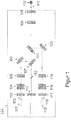
- FIG. 1 shows a first exemplary embodiment of a device with an array of optical elements.
- the device 122 has two laser light sources 101, 115.
- the laser light sources 101, 115 are suitable for generating laser light beams 102, 116 having different wavelengths.
- the generated laser light beams 102, 116 are guided on individual light paths, on which optical beam shaping devices 103, 117, for example lenses, optical isolators 104, 118 and bandpass filters 105, 119 are arranged.
- the light beams are deflected via mirrors 106, 120 to notch or notch filters 107, 121, wherein the notch or notch filters 107, 121 are arranged on a common light path, so that the light beams after deflection through the notch and notch filters 107, 121 cover a common light path.
- a further beam-shaping optical system 108 and a window 109 is arranged, wherein the further beam-shaping optical system 108 focuses the light beams onto a focal point and thus makes a sample 110, which is located in the focal point, accessible to a Raman analysis.
- Light 111 scattered back from the sample 110 is imaged through the window 109 and the further beam shaping optics 108 in the common light path.
- the scattered light then penetrates the notch filters 121, 107 in the opposite direction.
- the notch filters block the laser light and the elastically scattered portion of the scattered light.
- the Raman signals pass through the notch filters and encounter another beam-shaping optics 113.
- volume Bragg gratings may also be used.
- the notch or notch filters 107, 121 can also be replaced by volume Bragg gratings.
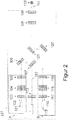
- FIG. 2 is another embodiment of in FIG. 1 shown embodiment shown.
- the laser sources 101, 115 are the associated optical beam shaping devices 103, 117, the associated optical isolators 104, 118 and the associated optical bandpass filters 105, 119 arranged in modules A, B, which are identical in mechanical structure to the laser wavelength of the laser light sources 101 and 115th
- the optode according to an embodiment of the invention is extended to a plurality of laser light sources.
- Modules A 1 to A n and B 1 to B n are arranged parallel to a parallel light deposit and suitable for emitting light of different wavelengths corresponding to parallel light paths spaced from the common light path.
- Mirrors M_A 1 to M_A n and M_B 1 to M_B n redirect the light beams at the parallel light paths to notch or notch filters F_A 1 to F_A n and F_B 1 to F_B n .
- the notch filters F_A 1 to F_A n and F_B 1 to F_B n are arranged on a common light path, which is arranged parallel to the individual light paths onto which the individual laser light beams were emitted. In this common light path, the light beams deflected by the notch filters are beamformed by a beam-shaping optical system O 1 and focused through a window W on a focusing point and a focusing region.
- a sample P located in the focus point or focus region scatters the excitation light through the window W and the beamforming optics O 1 (here O 1 now serves as collection optics) and the backscattered light passes the common light path in the reverse direction through the notch filters F_A 1 to F_A n and F_B 1 to F_B n back.
- the laser light and the elastically scattered light are blocked by the notch filters.
- the spectrally shifted Raman signals pass through the notch filters and are focused onto a fiber F by another beam shaping optics O 2 .
- the Raman signals coupled in here are transported via this fiber F to an evaluation unit.
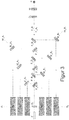
- FIGS. 4A to 4E show different constellations of sample positioning to the focal length of a common adjustable optic of an exemplary optode according to an embodiment of the invention.
- Figure 4A is shown as an excitation light 1 via an optical beam forming unit 02
- the beam forming unit 108 from the FIG. 1 corresponds, via a window 03, that of the window 109 FIG. 1 is focused on a focal point or a focus region with a distance a between the beam shaping unit 02 and window 03.
- a sample 04 which is located in the focal point or the focus region, scatters the excitation light 01 back as light 05.
- the light 05 is projected by the beam-shaping device 02 onto the optical beam-shaping device 07, that of the beam-shaping device 113 FIG. 1 equivalent.
- the beam shaping device 07 in turn focuses the light into a glass fiber 08.
- the FIG. 4B shows the analogous case to FIG. 4A
- sample 04 is no longer in the focus point, so that a maximum coupling of the Raman signal from the sample is no longer possible.
- FIG. 4C the out-of-focus positioning of the sample 04 occurs as a result of an intermediate layer of transparent or opaque material 09 arranged between the sample and the optode, which causes the focal point to be displaced.
- the Figures 5 and 6 show the transmission T of the 16 deflection devices of the preferred embodiment of the Fig. 3 depending on the absolute wave number ( Fig. 5 ) or the wavelength ( Fig. 6 ).
- Raman spectra in the range between 230 nm and 669 nm with the aid of 14 Excitation light sources can be measured.
- Raman spectra can thus be generated with the 14 excitation light sources and a suitable choice of the excitation wavelength can be made on the basis of the Raman spectra and properties of the sample.
- the central wavelengths of the excitation light sources are distributed uniformly over the spectrum with respect to the absolute wave number, ie are spaced equidistant from one another.
- wavenumber differences in the sense of the invention are then considered equal and thus the associated wavenumbers to be considered equidistant, if the wavenumber differences differ by less than 5% from each other.
- the distance is a minimum distance.
- the minimum distance may be about 10 cm -1 , 1000 cm -1 or 2000 cm -1 .
- the minimum distance guarantees a detection window between wave number adjacent excitation light sources, radiation inelastically scattered into the detection window can then be separated from elastically scattered radiation by means of the notch filters. With non-uniform distribution of the central wavelengths of the excitation light sources relative to the absolute wavenumber, observance of the minimum distance between adjacent excitation light source wavenumbers is also preferred.
- the distances between adjacent excitation light source wavenumbers are equal to the minimum distance or a multiple of the minimum distance.
- the width of the deflecting devices which are preferably designed as notch filters, is selected such that at least 99% of the elastically scattered radiation of the excitation light sources is deflected out of the collecting path.
- the width of the flanks of the 14 notch filters is kept as small as possible, so that between the notch filters a high transmission for the other wavelengths is provided, which correspond to the inelastic scattering of the light (Stokes range and anti-Stokes range).
Claims (12)
- Dispositif de spectroscopie Raman doté d'un an agencement d'éléments optiques, comprenant :une pluralité de n>2 sources de lumière d'excitation (A1 à An et B1 à Bn) servant à émettre n rayonnements d'excitation ayant des émissions différentes, respectivement, équidistantes les unes des autres en nombre d'ondes qui sont guidées le long d'un trajet lumineux d'une pluralité de n trajets lumineux différents, respectivement ;un dispositif de déviation (F_A1 à F_An et F_B1 à F_Bn) étant associé à chaque trajet lumineux, le dispositif de déviation étant formé sur le trajet lumineux associé, pour une première longueur d'onde respective du rayonnement d'excitation, afin de dévier le trajet lumineux respectif sur un trajet lumineux commun, le trajet lumineux commun comprenant un système optique (O1) formé pour focaliser les rayonnements d'excitation, au moins n-1 des dispositifs de déviation (F_A1 à F_An et F_B1 à F_Bn) comprenant une première transmission pour des longueurs d'onde d'une plage de longueurs d'onde respective située autour de la première longueur d'onde respective, etune seconde transmission pour d'autres longueurs d'onde respectives, respectivement, la première transmission étant inférieure à la seconde transmission, respectivement, et les plages de longueurs d'onde ne se chevauchant pas.
- Dispositif selon la revendication 1, dans lequel respectivement un montant d'une différence entre des longueurs d'onde se trouvant dans le spectre de rayonnements d'excitation adjacents les uns aux autres est supérieur à une somme de largeurs de bande des rayonnements d'excitation respectifs adjacents les uns aux autres.
- Dispositif selon l'une des revendications précédentes, dans lequel la distance en nombres d'onde entre des rayonnements d'excitation adjacents les uns aux autres dans le spectre est d'au moins 10 cm-1.
- Dispositif selon l'une des revendications précédentes, dans lequel également ledit tout au plus un dispositif de déviation restant comprend pour des longueurs d'onde d'une plage d'onde située sur le trajet lumineux associé au dispositif de déviation restant autour d'une première longueur d'onde associée du rayonnement d'excitation, et comprend une seconde transmission pour d'autres longueurs d'ondes associées, la première transmission étant inférieure à la seconde transmission dudit tout au plus un dispositif de déviation restant.
- Dispositif selon l'une des revendications précédentes, dans lequel les au moins n-1 dispositifs de déviation (F_A1 à F_An et F_B1 à F_Bn) sont formés en tant que filtres coupe-bande ou en tant que réseaux de Bragg en volume.
- Dispositif selon l'une des revendications précédentes, dans lequel la première transmission des au moins n-1 dispositifs de déviation (F_A1 à F_An et F_B1 à F_Bn) est inférieure à 0,5, respectivement.
- Dispositif selon l'une des revendications précédentes, dans lequel la seconde transmission des au moins n-1 dispositifs de déviation (F_A1 à F_An et F_B1 à F_Bn) est supérieure à 0,5.
- Dispositif selon l'une des revendications précédentes, dans lequel n est supérieur à 3.
- Dispositif selon l'une des revendications précédentes, dans lequel le dispositif comprend une fenêtre (W) et dans lequel le système optique (O1) peut être commandé, et une distance du système optique (O1) peut être ajustée par la fenêtre (W), et ainsi la position du point focal ou d'une région focale peut être ajustée à l'extérieur du dispositif en commandant le système optique (O1).
- Dispositif selon l'une des revendications précédentes, dans lequel des systèmes optiques de mise en forme de faisceau et/ou des filtres passe-bande sont disposés sur les trajets lumineux différents.
- Dispositif selon la revendication 9, dans lequel les sources de lumière d'excitation (A1 à An et B1 à Bn) sont dotées, sur les deux côtés d'un système de collecte optique compris en outre, d'un système optique de mise en forme d'un faisceau lumineux diffusé (O2) et d'un système optique de transfert (F) disposé de manière confocale par rapport au système optique (O1), le système optique de collecte étant adapté pour collectionner de la lumière d'un faisceau lumineux des faisceaux lumineux individuels diffusée par un objet (P) se trouvant dans le foyer via la fenêtre (W) et via le système optique (O1) et via un trajet de lumière de collecte comprenant le trajet lumineux commun, et de la fournir à une sortie.
- Dispositif selon l'une des revendications précédentes, dans lequel les sources de lumière d'excitation (A1 à An et B1 à Bn) sont des diodes laser qui peuvent respectivement être commandées à au moins deux conditions d'excitation différentes afin de générer du rayonnement d'excitation d'au moins deux longueurs d'onde différentes.
Applications Claiming Priority (2)
| Application Number | Priority Date | Filing Date | Title |
|---|---|---|---|
| DE102012216164.3A DE102012216164B4 (de) | 2012-09-12 | 2012-09-12 | Vorrichtung mit einer Anordnung optischer Elemente |
| PCT/EP2013/068938 WO2014041089A1 (fr) | 2012-09-12 | 2013-09-12 | Dispositif comprenant un agencement d'éléments optiques |
Publications (2)
| Publication Number | Publication Date |
|---|---|
| EP2895844A1 EP2895844A1 (fr) | 2015-07-22 |
| EP2895844B1 true EP2895844B1 (fr) | 2018-11-07 |
Family
ID=49328500
Family Applications (1)
| Application Number | Title | Priority Date | Filing Date |
|---|---|---|---|
| EP13774619.4A Active EP2895844B1 (fr) | 2012-09-12 | 2013-09-12 | Dispositif comprenant un agencement d'éléments optiques |
Country Status (6)
| Country | Link |
|---|---|
| US (1) | US9563061B2 (fr) |
| EP (1) | EP2895844B1 (fr) |
| JP (1) | JP6255022B2 (fr) |
| DE (1) | DE102012216164B4 (fr) |
| DK (1) | DK2895844T3 (fr) |
| WO (1) | WO2014041089A1 (fr) |
Families Citing this family (7)
| Publication number | Priority date | Publication date | Assignee | Title |
|---|---|---|---|---|
| US10746600B2 (en) * | 2015-01-09 | 2020-08-18 | California Institute Of Technology | Dual wavelength context imaging Raman and fluorescence spectrometer |
| RU2629703C1 (ru) * | 2016-05-16 | 2017-08-31 | Федеральное государственное бюджетное учреждение науки Институт электрофизики Уральского отделения Российской академии наук (ИЭФ УрО РАН) | Люминесцентный способ определения количественного содержания неоднородно распределенной дополнительной кристаллической фазы в сильнорассеивающих дисперсных двухфазных средах с примесными ионами-люминогенами |
| DE102016111747B4 (de) * | 2016-06-27 | 2020-10-01 | Forschungsverbund Berlin E.V. | Verfahren und Vorrichtung zur Raman-Spektroskopie |
| KR20180051196A (ko) * | 2016-11-08 | 2018-05-16 | 삼성전자주식회사 | 분광기, 생체정보 측정 장치 및 방법 |
| EP3601968A4 (fr) * | 2017-03-30 | 2020-12-16 | Agency for Science, Technology and Research | Sonde optique, système de spectroscopie raman, et procédé d'utilisation associé |
| JP7246466B2 (ja) | 2018-08-06 | 2023-03-27 | サーモ エレクトロン サイエンティフィック インストルメンツ リミテッド ライアビリティ カンパニー | 迷光低減を伴うモノクロメータ |
| CN109580587A (zh) * | 2019-02-01 | 2019-04-05 | 浙江澍源智能技术有限公司 | 一种可实时扣除荧光的差分拉曼光谱仪及其方法 |
Family Cites Families (18)
| Publication number | Priority date | Publication date | Assignee | Title |
|---|---|---|---|---|
| CA2048564C (fr) | 1990-08-16 | 2001-10-23 | Paul Graham Coombs | Dispositif antiparasite a variation optique et a suppression de cretes, et methode de fabrication |
| DE19956620A1 (de) * | 1999-11-25 | 2001-05-31 | Zeiss Carl Jena Gmbh | Verfahren zur Erfassung von Fluoreszenzerscheinungen in einem Mikroskop |
| EP1316794A1 (fr) * | 2001-11-28 | 2003-06-04 | Cambridge University Technical Services Limited | Analyseur de fluorescence optique à deux longueurs d'onde |
| US6897951B2 (en) * | 2003-02-14 | 2005-05-24 | Raman Systems, Inc. | Probe assemblies for Raman spectroscopy |
| GB2423579B (en) * | 2003-10-17 | 2008-04-09 | Intel Corp | A method and device for detecting small numbers of molecules using surface-enhanced coherent anti-stokes raman spectroscopy |
| US7245369B2 (en) * | 2003-11-13 | 2007-07-17 | B & W Tek, Inc. | Spectroscopic apparatus using spectrum narrowed and stabilized laser with Bragg grating |
| US7102746B2 (en) | 2003-12-16 | 2006-09-05 | New Chromex, Inc. | Raman spectroscope |
| US8105849B2 (en) * | 2004-02-27 | 2012-01-31 | Board Of Regents, The University Of Texas System | Integration of fluids and reagents into self-contained cartridges containing sensor elements |
| DE102004034998A1 (de) * | 2004-07-16 | 2006-02-02 | Carl Zeiss Jena Gmbh | Lichtrastermikroskop mit bewegter Lochscheibe und Verwendung |
| DE102004034977A1 (de) * | 2004-07-16 | 2006-02-02 | Carl Zeiss Jena Gmbh | Lichtrastermikroskop und Verwendung |
| DE102005054184B4 (de) | 2005-11-14 | 2020-10-29 | Carl Zeiss Microscopy Gmbh | Multispektrale Beleuchtungsvorrichtung und Messverfahren |
| DE102006048054A1 (de) * | 2006-10-11 | 2008-04-17 | Carl Zeiss Microimaging Gmbh | Multispektrale Beleuchtungseinrichtung |
| US7982869B2 (en) | 2006-10-24 | 2011-07-19 | Pd-Ld Inc. | Compact, low cost Raman monitor for single substances |
| JP2010160043A (ja) * | 2009-01-08 | 2010-07-22 | Panasonic Corp | 表面増強ラマン分光測定方法及び本方法を用いた表面増強ラマン分光装置 |
| JP5307629B2 (ja) * | 2009-05-22 | 2013-10-02 | オリンパス株式会社 | 走査型顕微鏡装置 |
| DE102009031231A1 (de) * | 2009-06-26 | 2010-12-30 | Carl Zeiss Microlmaging Gmbh | Verfahren und Anordnungen für die Fluoreszenzmikroskopie |
| JP5543760B2 (ja) * | 2009-11-24 | 2014-07-09 | オリンパス株式会社 | 光源装置、顕微鏡システムおよびレーザ光の合波方法 |
| US20120099102A1 (en) * | 2010-10-26 | 2012-04-26 | Bello Job M | Dual and multi-wavelength sampling probe for raman spectroscopy |
-
2012
- 2012-09-12 DE DE102012216164.3A patent/DE102012216164B4/de not_active Expired - Fee Related
-
2013
- 2013-09-12 US US14/427,437 patent/US9563061B2/en active Active
- 2013-09-12 JP JP2015531562A patent/JP6255022B2/ja active Active
- 2013-09-12 DK DK13774619.4T patent/DK2895844T3/en active
- 2013-09-12 WO PCT/EP2013/068938 patent/WO2014041089A1/fr active Application Filing
- 2013-09-12 EP EP13774619.4A patent/EP2895844B1/fr active Active
Non-Patent Citations (1)
| Title |
|---|
| None * |
Also Published As
| Publication number | Publication date |
|---|---|
| DE102012216164A1 (de) | 2014-03-13 |
| WO2014041089A1 (fr) | 2014-03-20 |
| DK2895844T3 (en) | 2019-03-04 |
| JP6255022B2 (ja) | 2017-12-27 |
| US9563061B2 (en) | 2017-02-07 |
| EP2895844A1 (fr) | 2015-07-22 |
| JP2015531874A (ja) | 2015-11-05 |
| US20150219906A1 (en) | 2015-08-06 |
| DE102012216164B4 (de) | 2016-04-28 |
Similar Documents
| Publication | Publication Date | Title |
|---|---|---|
| EP2895844B1 (fr) | Dispositif comprenant un agencement d'éléments optiques | |
| EP2156154B1 (fr) | Spectromètre doté de capteurs solides et de multiplicateurs d'électrons secondaires | |
| EP1754032B1 (fr) | Spectrometre-echelle a mise en valeur amelioree du detecteur par l'utilisation de deux ensembles spectrometres | |
| EP1891408B1 (fr) | Procede et dispositif pour generer et detecter un spectre de raman | |
| EP3309538B1 (fr) | Système optique et procédé de spectroscopie | |
| DE102010045856A1 (de) | Optisches Abbildungssystem zur multispektralen Bildgebung | |
| DE102007039845A1 (de) | Spektroskopie-System | |
| EP3465165B1 (fr) | Procédé et dispositif de spectroscopie raman | |
| WO2016096133A1 (fr) | Dispositif et procédé pour contrôler des substances caractéristiques | |
| DE102012007045B4 (de) | Vorrichtung und Verfahren zur Mikroskopie | |
| EP3217205A1 (fr) | Dispositif et procédé de microscopie par balayage multizone | |
| EP2282194A1 (fr) | Dispositif pour éffectuer des réactions PCR en temps réel | |
| DE102011100507B4 (de) | Tragbares optisches Analysegerät | |
| DE102015001032A1 (de) | Raman-Spektroskopie-Beleuchtungs- und Auslesesystem | |
| DE102017130772A1 (de) | Spektrometeranordnung, Verfahren zur Erzeugung eines zweidimensionalen Spektrums mittels einer solchen | |
| DE4413096B4 (de) | Multielement-Atomabsorptionsspektrometer sowie Meßverfahren unter Nutzung eines solchen Atomabsorptionsspektrometers | |
| EP3660474B1 (fr) | Dispositif et procédé de spectroscopie raman | |
| DE102005024271A1 (de) | Gitterspektrometersystem und Verfahren zur Messwerterfassung | |
| DE10155142A1 (de) | Dunkelfeld-Abbildungsvorrichtung zur ortsaufgelösten Dunkelfeldabbildung einer flächigen Probe | |
| DE102020131374B4 (de) | Fluoreszenzdetektion | |
| DE202013002752U1 (de) | Vorrichtung zur Ermittlung von Fluoreszenzeigenschaften von Proben | |
| DE102016110210B4 (de) | Spektrometer | |
| DE102010041748A1 (de) | Vorrichtungen und Verfahren zur spektroskopischen Untersuchung von Proben |
Legal Events
| Date | Code | Title | Description |
|---|---|---|---|
| PUAI | Public reference made under article 153(3) epc to a published international application that has entered the european phase |
Free format text: ORIGINAL CODE: 0009012 |
|
| 17P | Request for examination filed |
Effective date: 20150410 |
|
| AK | Designated contracting states |
Kind code of ref document: A1 Designated state(s): AL AT BE BG CH CY CZ DE DK EE ES FI FR GB GR HR HU IE IS IT LI LT LU LV MC MK MT NL NO PL PT RO RS SE SI SK SM TR |
|
| AX | Request for extension of the european patent |
Extension state: BA ME |
|
| DAX | Request for extension of the european patent (deleted) | ||
| GRAP | Despatch of communication of intention to grant a patent |
Free format text: ORIGINAL CODE: EPIDOSNIGR1 |
|
| STAA | Information on the status of an ep patent application or granted ep patent |
Free format text: STATUS: GRANT OF PATENT IS INTENDED |
|
| RIC1 | Information provided on ipc code assigned before grant |
Ipc: G02B 27/14 20060101ALI20180525BHEP Ipc: G01N 21/39 20060101ALN20180525BHEP Ipc: G01J 3/44 20060101ALI20180525BHEP Ipc: G01J 3/427 20060101ALI20180525BHEP Ipc: G01N 21/65 20060101AFI20180525BHEP |
|
| INTG | Intention to grant announced |
Effective date: 20180618 |
|
| GRAS | Grant fee paid |
Free format text: ORIGINAL CODE: EPIDOSNIGR3 |
|
| GRAA | (expected) grant |
Free format text: ORIGINAL CODE: 0009210 |
|
| STAA | Information on the status of an ep patent application or granted ep patent |
Free format text: STATUS: THE PATENT HAS BEEN GRANTED |
|
| AK | Designated contracting states |
Kind code of ref document: B1 Designated state(s): AL AT BE BG CH CY CZ DE DK EE ES FI FR GB GR HR HU IE IS IT LI LT LU LV MC MK MT NL NO PL PT RO RS SE SI SK SM TR |
|
| REG | Reference to a national code |
Ref country code: GB Ref legal event code: FG4D Free format text: NOT ENGLISH |
|
| REG | Reference to a national code |
Ref country code: CH Ref legal event code: EP Ref country code: AT Ref legal event code: REF Ref document number: 1062661 Country of ref document: AT Kind code of ref document: T Effective date: 20181115 |
|
| REG | Reference to a national code |
Ref country code: IE Ref legal event code: FG4D Free format text: LANGUAGE OF EP DOCUMENT: GERMAN |
|
| REG | Reference to a national code |
Ref country code: DE Ref legal event code: R096 Ref document number: 502013011560 Country of ref document: DE |
|
| REG | Reference to a national code |
Ref country code: CH Ref legal event code: NV Representative=s name: HEPP WENGER RYFFEL AG, CH |
|
| REG | Reference to a national code |
Ref country code: DK Ref legal event code: T3 Effective date: 20190225 |
|
| REG | Reference to a national code |
Ref country code: NL Ref legal event code: MP Effective date: 20181107 |
|
| REG | Reference to a national code |
Ref country code: LT Ref legal event code: MG4D |
|
| PG25 | Lapsed in a contracting state [announced via postgrant information from national office to epo] |
Ref country code: IS Free format text: LAPSE BECAUSE OF FAILURE TO SUBMIT A TRANSLATION OF THE DESCRIPTION OR TO PAY THE FEE WITHIN THE PRESCRIBED TIME-LIMIT Effective date: 20190307 Ref country code: ES Free format text: LAPSE BECAUSE OF FAILURE TO SUBMIT A TRANSLATION OF THE DESCRIPTION OR TO PAY THE FEE WITHIN THE PRESCRIBED TIME-LIMIT Effective date: 20181107 Ref country code: BG Free format text: LAPSE BECAUSE OF FAILURE TO SUBMIT A TRANSLATION OF THE DESCRIPTION OR TO PAY THE FEE WITHIN THE PRESCRIBED TIME-LIMIT Effective date: 20190207 Ref country code: NO Free format text: LAPSE BECAUSE OF FAILURE TO SUBMIT A TRANSLATION OF THE DESCRIPTION OR TO PAY THE FEE WITHIN THE PRESCRIBED TIME-LIMIT Effective date: 20190207 Ref country code: LT Free format text: LAPSE BECAUSE OF FAILURE TO SUBMIT A TRANSLATION OF THE DESCRIPTION OR TO PAY THE FEE WITHIN THE PRESCRIBED TIME-LIMIT Effective date: 20181107 Ref country code: HR Free format text: LAPSE BECAUSE OF FAILURE TO SUBMIT A TRANSLATION OF THE DESCRIPTION OR TO PAY THE FEE WITHIN THE PRESCRIBED TIME-LIMIT Effective date: 20181107 Ref country code: LV Free format text: LAPSE BECAUSE OF FAILURE TO SUBMIT A TRANSLATION OF THE DESCRIPTION OR TO PAY THE FEE WITHIN THE PRESCRIBED TIME-LIMIT Effective date: 20181107 |
|
| PG25 | Lapsed in a contracting state [announced via postgrant information from national office to epo] |
Ref country code: NL Free format text: LAPSE BECAUSE OF FAILURE TO SUBMIT A TRANSLATION OF THE DESCRIPTION OR TO PAY THE FEE WITHIN THE PRESCRIBED TIME-LIMIT Effective date: 20181107 Ref country code: AL Free format text: LAPSE BECAUSE OF FAILURE TO SUBMIT A TRANSLATION OF THE DESCRIPTION OR TO PAY THE FEE WITHIN THE PRESCRIBED TIME-LIMIT Effective date: 20181107 Ref country code: SE Free format text: LAPSE BECAUSE OF FAILURE TO SUBMIT A TRANSLATION OF THE DESCRIPTION OR TO PAY THE FEE WITHIN THE PRESCRIBED TIME-LIMIT Effective date: 20181107 Ref country code: GR Free format text: LAPSE BECAUSE OF FAILURE TO SUBMIT A TRANSLATION OF THE DESCRIPTION OR TO PAY THE FEE WITHIN THE PRESCRIBED TIME-LIMIT Effective date: 20190208 Ref country code: RS Free format text: LAPSE BECAUSE OF FAILURE TO SUBMIT A TRANSLATION OF THE DESCRIPTION OR TO PAY THE FEE WITHIN THE PRESCRIBED TIME-LIMIT Effective date: 20181107 Ref country code: PT Free format text: LAPSE BECAUSE OF FAILURE TO SUBMIT A TRANSLATION OF THE DESCRIPTION OR TO PAY THE FEE WITHIN THE PRESCRIBED TIME-LIMIT Effective date: 20190307 |
|
| PG25 | Lapsed in a contracting state [announced via postgrant information from national office to epo] |
Ref country code: PL Free format text: LAPSE BECAUSE OF FAILURE TO SUBMIT A TRANSLATION OF THE DESCRIPTION OR TO PAY THE FEE WITHIN THE PRESCRIBED TIME-LIMIT Effective date: 20181107 Ref country code: CZ Free format text: LAPSE BECAUSE OF FAILURE TO SUBMIT A TRANSLATION OF THE DESCRIPTION OR TO PAY THE FEE WITHIN THE PRESCRIBED TIME-LIMIT Effective date: 20181107 |
|
| REG | Reference to a national code |
Ref country code: DE Ref legal event code: R097 Ref document number: 502013011560 Country of ref document: DE |
|
| PG25 | Lapsed in a contracting state [announced via postgrant information from national office to epo] |
Ref country code: SK Free format text: LAPSE BECAUSE OF FAILURE TO SUBMIT A TRANSLATION OF THE DESCRIPTION OR TO PAY THE FEE WITHIN THE PRESCRIBED TIME-LIMIT Effective date: 20181107 Ref country code: RO Free format text: LAPSE BECAUSE OF FAILURE TO SUBMIT A TRANSLATION OF THE DESCRIPTION OR TO PAY THE FEE WITHIN THE PRESCRIBED TIME-LIMIT Effective date: 20181107 Ref country code: EE Free format text: LAPSE BECAUSE OF FAILURE TO SUBMIT A TRANSLATION OF THE DESCRIPTION OR TO PAY THE FEE WITHIN THE PRESCRIBED TIME-LIMIT Effective date: 20181107 Ref country code: SM Free format text: LAPSE BECAUSE OF FAILURE TO SUBMIT A TRANSLATION OF THE DESCRIPTION OR TO PAY THE FEE WITHIN THE PRESCRIBED TIME-LIMIT Effective date: 20181107 |
|
| PLBE | No opposition filed within time limit |
Free format text: ORIGINAL CODE: 0009261 |
|
| STAA | Information on the status of an ep patent application or granted ep patent |
Free format text: STATUS: NO OPPOSITION FILED WITHIN TIME LIMIT |
|
| 26N | No opposition filed |
Effective date: 20190808 |
|
| PG25 | Lapsed in a contracting state [announced via postgrant information from national office to epo] |
Ref country code: SI Free format text: LAPSE BECAUSE OF FAILURE TO SUBMIT A TRANSLATION OF THE DESCRIPTION OR TO PAY THE FEE WITHIN THE PRESCRIBED TIME-LIMIT Effective date: 20181107 |
|
| PG25 | Lapsed in a contracting state [announced via postgrant information from national office to epo] |
Ref country code: TR Free format text: LAPSE BECAUSE OF FAILURE TO SUBMIT A TRANSLATION OF THE DESCRIPTION OR TO PAY THE FEE WITHIN THE PRESCRIBED TIME-LIMIT Effective date: 20181107 |
|
| PG25 | Lapsed in a contracting state [announced via postgrant information from national office to epo] |
Ref country code: MC Free format text: LAPSE BECAUSE OF FAILURE TO SUBMIT A TRANSLATION OF THE DESCRIPTION OR TO PAY THE FEE WITHIN THE PRESCRIBED TIME-LIMIT Effective date: 20181107 |
|
| PG25 | Lapsed in a contracting state [announced via postgrant information from national office to epo] |
Ref country code: IE Free format text: LAPSE BECAUSE OF NON-PAYMENT OF DUE FEES Effective date: 20190912 Ref country code: LU Free format text: LAPSE BECAUSE OF NON-PAYMENT OF DUE FEES Effective date: 20190912 |
|
| REG | Reference to a national code |
Ref country code: BE Ref legal event code: MM Effective date: 20190930 |
|
| PG25 | Lapsed in a contracting state [announced via postgrant information from national office to epo] |
Ref country code: BE Free format text: LAPSE BECAUSE OF NON-PAYMENT OF DUE FEES Effective date: 20190930 |
|
| PG25 | Lapsed in a contracting state [announced via postgrant information from national office to epo] |
Ref country code: FR Free format text: LAPSE BECAUSE OF NON-PAYMENT OF DUE FEES Effective date: 20190930 |
|
| REG | Reference to a national code |
Ref country code: AT Ref legal event code: MM01 Ref document number: 1062661 Country of ref document: AT Kind code of ref document: T Effective date: 20190912 |
|
| PG25 | Lapsed in a contracting state [announced via postgrant information from national office to epo] |
Ref country code: AT Free format text: LAPSE BECAUSE OF NON-PAYMENT OF DUE FEES Effective date: 20190912 |
|
| REG | Reference to a national code |
Ref country code: DE Ref legal event code: R082 Ref document number: 502013011560 Country of ref document: DE Representative=s name: GULDE & PARTNER PATENT- UND RECHTSANWALTSKANZL, DE Ref country code: DE Ref legal event code: R081 Ref document number: 502013011560 Country of ref document: DE Owner name: FERDINAND-BRAUN-INSTITUT GGMBH, LEIBNIZ- INSTI, DE Free format text: FORMER OWNER: FORSCHUNGSVERBUND BERLIN E.V., 12489 BERLIN, DE |
|
| PG25 | Lapsed in a contracting state [announced via postgrant information from national office to epo] |
Ref country code: CY Free format text: LAPSE BECAUSE OF FAILURE TO SUBMIT A TRANSLATION OF THE DESCRIPTION OR TO PAY THE FEE WITHIN THE PRESCRIBED TIME-LIMIT Effective date: 20181107 |
|
| PG25 | Lapsed in a contracting state [announced via postgrant information from national office to epo] |
Ref country code: HU Free format text: LAPSE BECAUSE OF FAILURE TO SUBMIT A TRANSLATION OF THE DESCRIPTION OR TO PAY THE FEE WITHIN THE PRESCRIBED TIME-LIMIT; INVALID AB INITIO Effective date: 20130912 Ref country code: MT Free format text: LAPSE BECAUSE OF FAILURE TO SUBMIT A TRANSLATION OF THE DESCRIPTION OR TO PAY THE FEE WITHIN THE PRESCRIBED TIME-LIMIT Effective date: 20181107 |
|
| REG | Reference to a national code |
Ref country code: FI Ref legal event code: PCE Owner name: FERDINAND-BRAUN-INSTITUT GGMBH, LEIBNIZ-INSTITUT FUER HOECHSTFREQUENZTECHNIK |
|
| PG25 | Lapsed in a contracting state [announced via postgrant information from national office to epo] |
Ref country code: MK Free format text: LAPSE BECAUSE OF FAILURE TO SUBMIT A TRANSLATION OF THE DESCRIPTION OR TO PAY THE FEE WITHIN THE PRESCRIBED TIME-LIMIT Effective date: 20181107 |
|
| REG | Reference to a national code |
Ref country code: GB Ref legal event code: 732E Free format text: REGISTERED BETWEEN 20230323 AND 20230329 |
|
| PGFP | Annual fee paid to national office [announced via postgrant information from national office to epo] |
Ref country code: GB Payment date: 20230921 Year of fee payment: 11 Ref country code: FI Payment date: 20230918 Year of fee payment: 11 |
|
| PGFP | Annual fee paid to national office [announced via postgrant information from national office to epo] |
Ref country code: DK Payment date: 20230921 Year of fee payment: 11 Ref country code: DE Payment date: 20230830 Year of fee payment: 11 |
|
| PGFP | Annual fee paid to national office [announced via postgrant information from national office to epo] |
Ref country code: IT Payment date: 20230929 Year of fee payment: 11 Ref country code: CH Payment date: 20231001 Year of fee payment: 11 |