EP2891908A1 - Teilungselement für polarisiertes uv-licht - Google Patents
Teilungselement für polarisiertes uv-licht Download PDFInfo
- Publication number
- EP2891908A1 EP2891908A1 EP13833108.7A EP13833108A EP2891908A1 EP 2891908 A1 EP2891908 A1 EP 2891908A1 EP 13833108 A EP13833108 A EP 13833108A EP 2891908 A1 EP2891908 A1 EP 2891908A1
- Authority
- EP
- European Patent Office
- Prior art keywords
- ultraviolet light
- splitting element
- polarized ultraviolet
- light splitting
- light
- Prior art date
- Legal status (The legal status is an assumption and is not a legal conclusion. Google has not performed a legal analysis and makes no representation as to the accuracy of the status listed.)
- Granted
Links
Images

Classifications
-
- G—PHYSICS
- G02—OPTICS
- G02F—OPTICAL DEVICES OR ARRANGEMENTS FOR THE CONTROL OF LIGHT BY MODIFICATION OF THE OPTICAL PROPERTIES OF THE MEDIA OF THE ELEMENTS INVOLVED THEREIN; NON-LINEAR OPTICS; FREQUENCY-CHANGING OF LIGHT; OPTICAL LOGIC ELEMENTS; OPTICAL ANALOGUE/DIGITAL CONVERTERS
- G02F1/00—Devices or arrangements for the control of the intensity, colour, phase, polarisation or direction of light arriving from an independent light source, e.g. switching, gating or modulating; Non-linear optics
- G02F1/01—Devices or arrangements for the control of the intensity, colour, phase, polarisation or direction of light arriving from an independent light source, e.g. switching, gating or modulating; Non-linear optics for the control of the intensity, phase, polarisation or colour
- G02F1/13—Devices or arrangements for the control of the intensity, colour, phase, polarisation or direction of light arriving from an independent light source, e.g. switching, gating or modulating; Non-linear optics for the control of the intensity, phase, polarisation or colour based on liquid crystals, e.g. single liquid crystal display cells
- G02F1/133—Constructional arrangements; Operation of liquid crystal cells; Circuit arrangements
- G02F1/1333—Constructional arrangements; Manufacturing methods
- G02F1/1335—Structural association of cells with optical devices, e.g. polarisers or reflectors
-
- G—PHYSICS
- G02—OPTICS
- G02B—OPTICAL ELEMENTS, SYSTEMS OR APPARATUS
- G02B27/00—Optical systems or apparatus not provided for by any of the groups G02B1/00 - G02B26/00, G02B30/00
- G02B27/28—Optical systems or apparatus not provided for by any of the groups G02B1/00 - G02B26/00, G02B30/00 for polarising
- G02B27/283—Optical systems or apparatus not provided for by any of the groups G02B1/00 - G02B26/00, G02B30/00 for polarising used for beam splitting or combining
-
- G—PHYSICS
- G02—OPTICS
- G02B—OPTICAL ELEMENTS, SYSTEMS OR APPARATUS
- G02B5/00—Optical elements other than lenses
- G02B5/20—Filters
-
- G—PHYSICS
- G02—OPTICS
- G02B—OPTICAL ELEMENTS, SYSTEMS OR APPARATUS
- G02B5/00—Optical elements other than lenses
- G02B5/20—Filters
- G02B5/208—Filters for use with infrared or ultraviolet radiation, e.g. for separating visible light from infrared and/or ultraviolet radiation
-
- G—PHYSICS
- G02—OPTICS
- G02B—OPTICAL ELEMENTS, SYSTEMS OR APPARATUS
- G02B5/00—Optical elements other than lenses
- G02B5/30—Polarising elements
-
- G—PHYSICS
- G02—OPTICS
- G02B—OPTICAL ELEMENTS, SYSTEMS OR APPARATUS
- G02B5/00—Optical elements other than lenses
- G02B5/30—Polarising elements
- G02B5/3025—Polarisers, i.e. arrangements capable of producing a definite output polarisation state from an unpolarised input state
- G02B5/3058—Polarisers, i.e. arrangements capable of producing a definite output polarisation state from an unpolarised input state comprising electrically conductive elements, e.g. wire grids, conductive particles
-
- G—PHYSICS
- G02—OPTICS
- G02B—OPTICAL ELEMENTS, SYSTEMS OR APPARATUS
- G02B5/00—Optical elements other than lenses
- G02B5/30—Polarising elements
- G02B5/3025—Polarisers, i.e. arrangements capable of producing a definite output polarisation state from an unpolarised input state
- G02B5/3075—Polarisers, i.e. arrangements capable of producing a definite output polarisation state from an unpolarised input state for use in the UV
-
- G—PHYSICS
- G02—OPTICS
- G02F—OPTICAL DEVICES OR ARRANGEMENTS FOR THE CONTROL OF LIGHT BY MODIFICATION OF THE OPTICAL PROPERTIES OF THE MEDIA OF THE ELEMENTS INVOLVED THEREIN; NON-LINEAR OPTICS; FREQUENCY-CHANGING OF LIGHT; OPTICAL LOGIC ELEMENTS; OPTICAL ANALOGUE/DIGITAL CONVERTERS
- G02F1/00—Devices or arrangements for the control of the intensity, colour, phase, polarisation or direction of light arriving from an independent light source, e.g. switching, gating or modulating; Non-linear optics
- G02F1/01—Devices or arrangements for the control of the intensity, colour, phase, polarisation or direction of light arriving from an independent light source, e.g. switching, gating or modulating; Non-linear optics for the control of the intensity, phase, polarisation or colour
- G02F1/13—Devices or arrangements for the control of the intensity, colour, phase, polarisation or direction of light arriving from an independent light source, e.g. switching, gating or modulating; Non-linear optics for the control of the intensity, phase, polarisation or colour based on liquid crystals, e.g. single liquid crystal display cells
- G02F1/1313—Devices or arrangements for the control of the intensity, colour, phase, polarisation or direction of light arriving from an independent light source, e.g. switching, gating or modulating; Non-linear optics for the control of the intensity, phase, polarisation or colour based on liquid crystals, e.g. single liquid crystal display cells specially adapted for a particular application
-
- G—PHYSICS
- G21—NUCLEAR PHYSICS; NUCLEAR ENGINEERING
- G21K—HANDLING OF PARTICLES OR IONISING RADIATION NOT OTHERWISE PROVIDED FOR; IRRADIATION DEVICES; GAMMA RAY OR X-RAY MICROSCOPES
- G21K1/00—Arrangements for handling particles or ionising radiation, e.g. focusing or moderating
- G21K1/16—Arrangements for handling particles or ionising radiation, e.g. focusing or moderating using polarising devices, e.g. for obtaining a polarised beam
-
- G—PHYSICS
- G21—NUCLEAR PHYSICS; NUCLEAR ENGINEERING
- G21K—HANDLING OF PARTICLES OR IONISING RADIATION NOT OTHERWISE PROVIDED FOR; IRRADIATION DEVICES; GAMMA RAY OR X-RAY MICROSCOPES
- G21K5/00—Irradiation devices
- G21K5/04—Irradiation devices with beam-forming means
-
- G—PHYSICS
- G02—OPTICS
- G02F—OPTICAL DEVICES OR ARRANGEMENTS FOR THE CONTROL OF LIGHT BY MODIFICATION OF THE OPTICAL PROPERTIES OF THE MEDIA OF THE ELEMENTS INVOLVED THEREIN; NON-LINEAR OPTICS; FREQUENCY-CHANGING OF LIGHT; OPTICAL LOGIC ELEMENTS; OPTICAL ANALOGUE/DIGITAL CONVERTERS
- G02F1/00—Devices or arrangements for the control of the intensity, colour, phase, polarisation or direction of light arriving from an independent light source, e.g. switching, gating or modulating; Non-linear optics
- G02F1/01—Devices or arrangements for the control of the intensity, colour, phase, polarisation or direction of light arriving from an independent light source, e.g. switching, gating or modulating; Non-linear optics for the control of the intensity, phase, polarisation or colour
- G02F1/13—Devices or arrangements for the control of the intensity, colour, phase, polarisation or direction of light arriving from an independent light source, e.g. switching, gating or modulating; Non-linear optics for the control of the intensity, phase, polarisation or colour based on liquid crystals, e.g. single liquid crystal display cells
- G02F1/133—Constructional arrangements; Operation of liquid crystal cells; Circuit arrangements
- G02F1/1333—Constructional arrangements; Manufacturing methods
- G02F1/1337—Surface-induced orientation of the liquid crystal molecules, e.g. by alignment layers
- G02F1/13378—Surface-induced orientation of the liquid crystal molecules, e.g. by alignment layers by treatment of the surface, e.g. embossing, rubbing or light irradiation
- G02F1/133788—Surface-induced orientation of the liquid crystal molecules, e.g. by alignment layers by treatment of the surface, e.g. embossing, rubbing or light irradiation by light irradiation, e.g. linearly polarised light photo-polymerisation
Definitions
- the present invention relates to a polarized ultraviolet light splitting element and an application thereof.
- Liquid crystal alignment layers used in aligning liquid crystal molecules in a certain direction are being applied to various fields.
- a photo alignment layer has a surface treated by radiating light so that adjacent liquid crystal molecules are aligned.
- the photo alignment layer may be fabricated by irradiating a photosensitive material layer with light, for example, linearly polarized light to align the photosensitive material in a certain direction.
- polarized ultraviolet light splitting elements In order to irradiate the photo alignment layer with a linearly polarized light, various types of polarized ultraviolet light splitting elements may be used.
- Patent Literature 1 a polarized ultraviolet light splitting element using aluminum is disclosed in the following Patent Literature 1.
- Patent Literature 1 Korean Patent Publication No. 2002-0035587
- An object of the present invention is to provide a polarized ultraviolet light splitting element and an application thereof.
- Exemplary embodiments of the present invention relate to a polarized ultraviolet light splitting element.
- the term “polarized ultraviolet light splitting element” may refer to all kinds of elements configured to extract polarized ultraviolet light among light incident to the element.
- the polarized light may be linearly polarized light, circularly polarized light, or elliptically polarized light.
- the polarized light may be linearly polarized light.
- the term "ultraviolet light” used in the present specification, for example, may refer to an electromagnetic wave in a wavelength range of about 250 to 350 nm, about 270 to 330 nm, or about 290 to 310 nm.
- a polarized ultraviolet light splitting element may include a substrate layer and a convex portion formed on the substrate layer.
- the convex portion may include a titanium metal composite oxide.
- the convex portion may have a stripe shape, and at least two convex portions may be formed on the substrate layer.
- the stripe-shaped convex portions may be disposed substantially in parallel on the substrate layer.
- the number of the stripe-shaped convex portions on the substrate layer is not particularly limited and may be selected by considering, for example, an intensity of ultraviolet light to be split.
- the convex portions may exist by about 5 to 20 line/ ⁇ m on the substrate layer.
- the polarized ultraviolet light splitting element may have excellent light splitting efficiency with respect to light in a wide wavelength range, for example, ultraviolet light in a wide wavelength range.
- the light splitting efficiency of the polarized ultraviolet light splitting element may be defined by a polarization extinction ratio.
- the term "polarization extinction ratio" used in the present specification may refer to a ratio of an intensity of polarized light having a vector perpendicular to the convex portion to an intensity of polarized light having a vector parallel to the convex portion among light passing through the polarized ultraviolet light splitting element.
- the polarized ultraviolet light splitting element may show light splitting characteristics by transmitting the light having a vector perpendicular to the convex portion (so called P polarized light) and reflecting the light having a vector parallel to the convex portion (so called S polarized light).
- the light splitting efficiency may be defined by ratio of P polarized light to S polarized light.
- R calculated by the following Equation 1 may be two or more, 15 or more, 20 or more, 25 or more, 30 or more, 35 or more, 40 or more, or 45 or more in the polarized ultraviolet light splitting clement.
- the upper limit of R calculated by Equation 1 is not particularly limited. That is, the greater R indicates the greater light splitting efficiency. In respect of practicality, R may be, for example, 2,000 or less, 1,500 or less, 1,000 or less, 900 or less, 800 or less, 700 or less, 600 or less, 500 or less, 400 or less, 300 or less, 200 or less, or 150 or less.
- R Tc / Tp
- Tc represents a transmission rate of light polarized in a perpendicular direction to the stripe-shaped convex portion and having a wavelength of about 250 to 350 nm with respect to the polarized ultraviolet light splitting element
- Tp represents a transmission rate of light polarized in a parallel direction to the stripe-shaped convex portion and having a wavelength of about 250 to 350 nm with respect to the polarized ultraviolet light splitting element.
- the wavelength of light applied to Equation 1 may be about 270 to 330 nm, or about 290 to 310 nm.
- the polarized ultraviolet light splitting element may show an excellent transmission rate.
- transmission rate may refer to an intensity of light transmitted through the polarized ultraviolet light splitting element and having a vector perpendicular to the convex portion (P polarized light) among light radiated to the polarized ultraviolet light splitting element, for example, ultraviolet light.
- P calculated by the following Equation 2 may be 0.2 to 0.5 in the polarized ultraviolet light splitting element.
- P Tc / T
- T represents an intensity of light radiated to the polarized ultraviolet light splitting element and having a wavelength of about 250 to 350 nm
- Tc represents an intensity of light transmitted through the polarized ultraviolet light splitting element among the radiated light, polarized in a perpendicular direction to the stripe-shaped convex portion, and having a wavelength of about 250 to 350 nm.
- the wavelength of light applied to Equation 2 may be about 270 to 330 nm, or about 290 to 310 nm.
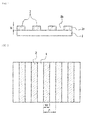
- FIG. 1 schematically shows a cross-section of a polarized ultraviolet light splitting element according to an exemplary embodiment of the present invention
- FIG. 2 schematically shows a top view of a polarized ultraviolet light splitting element according to an exemplary embodiment of the present invention
- the polarized ultraviolet light splitting element may include a substrate layer 1 and a concavo-convex pattern 2 formed on the substrate layer 1.
- Convex portions 2a configuring the concavo-convex pattern 2 may be arranged in parallel in a stripe shape as shown in FIG. 2 .
- a concave portion 2b may be formed by the convex portions 2a.
- the pitch, width, and height of the convex portion 2a may be adjusted to satisfy a splitting performance with respect to ultraviolet light, for example, the polarization extinction ratio and the transmission rate.
- the term "pitch P" refers to a length obtained by adding a width W of the convex portion 2a to a width of the concave portion 2b (see FIG.
- the term "height" refers to a height H of the convex portion 2a (see FIG. 1 ).
- the height is a height of the highest convex portion, or an average height of the convex portions 2a.
- the convex portion 2a may include a titanium metal composite oxide.
- the composite oxide may include, for example, a doped titanium oxide.
- the composite oxide may have a transmission rate of less than 10%, less than 5 %, less than 3 %, less than 2 %, less than 1 %, less than 0.2 %, or less than 0.1 % at a wavelength of 350 nm, and the lower limit may be, but not particularly limited thereto, about 0.01 % or 0.001 %.
- the transmission rate may be obtained by measuring the polarized ultraviolet light splitting element having a thickness of 100 nm using a conventional transmission rate measuring apparatus.
- the light splitting efficiency may be ensured in a wider ultraviolet wavelength range than when the existing titanium oxide or aluminum is used.
- the type or amount of a metal included in the composite oxide may be selected in such a manner that the composite oxide has the above-described transmission rate and, as long as selected in this way, may not be particularly limited.
- the titanium metal composite oxide may include titanium, and one or more second metals selected from Ni, Cr, Cu, Fe, B, V, Nb, Sb, Sn, Si, and Al.
- the second metal may be Ni or Cr.
- the ratio of the second metal in the composite oxide may be selected by considering the above-described transmission rate, for example, 1 to 20 mol %, 2 to 18 mol %, or 3 to 15 mol%.
- the composite oxide may be represented by the following Chemical Formula. [Chemical Formula 1] Ti x M y O 2
- M is one or more metals selected from the group consisting of Ni, Cr, Cu, Fe, B, V, Nb, Sb, Sn, Si, or Al, y is 0.01 to 0.2, and (x+y) is 1. In other embodiments, M may be Ni or Cr. In still other embodiments, y may be 0.05 to 0.15, or 0.07 to 1.13.
- the pitch P of the convex portion may be, for example, 50 to 200 nm, 100 to 180 nm, 110 to 150 nm, 120 to 150 nm, 130 to 150 nm, or 140 to 150 nm.
- a proper light splitting efficiency may not be ensured.
- a dielectric material may exist in the concave portion 2b formed by the convex portion 2a.
- a refractive index of the dielectric material with respect to light having a wavelength range of 250 to 350 nm may be one to five.
- the dielectric material may not be particularly limited, as long as it has the above-described range of refractive index.
- the dielectric material may be silicon oxide, magnesium fluoride, silicon nitride, or air.
- the concave portion 2b of the concavo-convex pattern 2 may be substantially an empty space.
- the ultraviolet light polarized ultraviolet light splitting element may have a in the range of 0.74 to 10 and b in the range of 0.5 to 10, which are calculated by the following Equation 3.
- Equation 3 i is an imaginary number unit, n 1 is a refractive index of the dielectric material with respect to ultraviolet light having a wavelength within the wavelength range of 250 to 350 nm, for example, 300 nm wavelength, n 2 is a refractive index of the convex portion 2a with respect to ultraviolet light having a wavelength within the wavelength range of 250 to 350 nm, for example, 300 nm wavelength, W is a width of the convex portion 2a, and P is a pitch of the convex portion 2a.
- a polarized ultraviolet light splitting element having a high degree of polarization of 0.5 or more, 0.6 or more, 0.7 or more, or 0.9 or more in a short wavelength range, for example, in a light wavelength range of 250 to 350 nm may be obtained even in a pitch range of 120 nm or more.
- the upper limit of the polarized light may be, but not particularly limited thereto, 0.98 or less, 0.95 or less, or 0.93 or less in respect of the economic efficiency of a fabrication process.
- the degree of polarization when the degree of polarization is more than 0.98, an aspect ratio (width/height of the convex portion 2a) of the convex portion 2a of the polarized ultraviolet light splitting element may be increased. Accordingly, the polarized ultraviolet light splitting element may be difficult to be fabricated, and the manufacturing process may be complicated.
- the term "degree of polarization” may refer to an intensity of polarized light with respect to an intensity of the incident light, and the degree of polarization may be calculated as the following Equation 4.
- Degree of Polarization D Tc - Tp / Tc + Tp
- Tc represents a transmission rate of light polarized in a perpendicular direction to the convex portion 2a and having a wavelength of about 250 to 350 nm with respect to the polarized ultraviolet light splitting element
- Tp represents a transmission rate of light polarized in a parallel direction to the convex portion 2a and having a wavelength of about 250 to 350 nm with respect to the polarized ultraviolet light splitting element.
- parallel refers to “substantially parallel”
- perpendicular refers to "substantially perpendicular.”
- c may be 1.3 to 10 and d may be 0.013 to 0.1 in the ultraviolet light polarized ultraviolet light splitting element, which are calculated by the following Equation 5.
- c + di 2 n 1 2 ⁇ n 2 2 / 1 - W / P ⁇ n 2 2 + W ⁇ n 1 2 / P
- Equation 5 i is an imaginary number unit, n 1 is a refractive index of the dielectric material with respect to ultraviolet light having a wavelength within the wavelength range of 250 to 350 nm, for example, a 300 nm wavelength, n 2 is a refractive index of the convex portion 2a with respect to ultraviolet light having a wavelength within the wavelength range of 250 to 350 nm, for example, a 300 nm wavelength, W is a width of the convex portion 2a, and P is a pitch of the convex portion 2a.
- the height H of the convex portion 2a may be, but not particularly limited thereto, for example, 20 to 300 nm, 50 to 200 nm, 100 to 150 nm, 150 to 250 nm, or 200 or 280 nm.
- the absolute amount of light may be lowered since the amount of absorbed light increases.
- a proper polarized ultraviolet light splitting element may be fabricated since the amount of absorbed light is not so much. Accordingly, the polarized ultraviolet light splitting element may have a good polarized light splitting performance while maintaining an excellent ultraviolet light transmission rate.
- degradation in the ease of fabricating a pattern due to an increase of the aspect ratio caused by an increase of the height H of the convex portion 2a under the same pitch P may be prevented.
- the width W of the convex portion 2a may be, but not limited thereto, for example, 10 to 160 nm.
- the width W of the convex portion 2a may be 10 to 120 nm, 30 to 100 nm, or 50 to 80 nm,
- a fill-factor of the convex portion may be 0.2 to 0.8, for example, 0.3 to 0.6, 0.4 to 0.7, 0.5 to 0.75, or 0.45.
- the polarized ultraviolet light splitting element may show a good polarized light splitting performance, and degradation in polarization characteristics of the polarized ultraviolet light splitting element may be prevented since the amount of absorbed light is not so much.
- the term "fill-factor of the convex portion" used in the present specification refers to a ratio of the width W of the convex portion to the pitch P of the convex portion.
- a may be 0.74 to 10 and b may be 0.5 to 10, which are calculated by the following Equation 6, and c may be 1.3 to 10 and d may be 0.013 to 0.1, which are calculated by the following Equation 7.
- Equation 6 and Equation 7 i is an imaginary number unit, and n 1 is a refractive index of the dielectric material with respect to ultraviolet light having a wavelength within the wavelength range of 250 to 350 nm, for example, 300 nm wavelength, n 2 is a refractive index of the convex portion 2a with respect to ultraviolet light having a wavelength within the wavelength range of 250 to 350 nm, for example, 300 nm wavelength, W is a width of the convex portion 2a, and P is a pitch of the convex portion 2a.
- the polarized ultraviolet light splitting element is designed in such a way that a, b, c, and d are within the above-described ranges by Equation 6 and Equation 7, an excellent degree of polarization and extinction ratio may be implemented even in a short wavelength range.
- the type of the substrate layer included in the polarized ultraviolet light splitting element may be, but not limited thereto, for example, quartz, ultraviolet light transmitting glass, polyvinyl alcohol (PVA), poly carbonate, ethylene vinyl acetate (EVA) copolymer, etc.
- the ultraviolet light transmission rate of the substrate layer 1 may be, for example, 70 % or more, 80 % or more, or 90 % or more. When the transmission rate is within the above-described range, the ultraviolet light transmission rate of the polarized ultraviolet light splitting element may be improved, and a photo alignment layer having an excellent photo alignment speed may be fabricated.
- the polarized ultraviolet light splitting element may be, for example, fabricated using a well-known method of forming a wire grid.
- the polarized ultraviolet light splitting element may be fabricated by forming the composite oxide layer on the substrate layer and selectively removing the composite oxide layer to be patterned.
- the composite oxide layer may be, for example, formed by a normal co-deposition method, or a well-known method, such as a sol-gel method, a solid-phase method, a hydrothermal method, a sputtering method, or a chemical vapor deposition (CVD) method.
- the composite oxide layer initially patterned by another well-known pattern forming method for example, a deposition method using a mask, may be formed on the substrate layer.
- the polarized ultraviolet light splitting element may be fabricated by forming a titanium metal composite oxide layer on the substrate layer and patterning the titanium metal composite oxide layer.
- the composite oxide layer may be formed on a substrate layer including an anti-reflection layer formed on a surface thereof.
- the anti-reflection layer may function to prevent degradation of efficiency due to an internal reflection or indirect reflection of a laser while a grid is formed on the metal composite oxide layer, for example, by laser interference lithography and form a finer grid.
- a material and a manufacturing method of the anti-reflection layer may not be limited as long as it is formed to absorb an internally reflected laser.
- a method of patterning the metal composite oxide layer formed on the substrate layer may be, but not limited thereto, for example, well-known photolithography, or laser interference lithography, e-bean lithography, nano imprint lithography (NIL), immersion lithography, or a sol-gel method in order to form a pattern having a finer pitch.
- NIL is a method of forming a pattern having a predetermined line width.
- the method may include forming a resist layer on a metal layer, then engraving a stamp patterned in a preferred line width at constant temperature and pressure with respect to the substrate layer on which the resist layer is formed on an imprint resist film, and then removing the remaining metal layer using plasma.
- Such a method may be particularly appropriate for forming of a fine pattern.
- an apparatus including the polarized ultraviolet light splitting element for example, a light illuminating apparatus.
- the light illuminating apparatus may include the polarized ultraviolet light splitting element and a subject mounting device.
- the polarized ultraviolet light splitting element may function as a polarization plate.
- the polarized ultraviolet light splitting element may be used to generate a linearly polarized light from a light radiated from a light source.
- the light illuminating apparatus may further include a photo alignment mask between the subject mounting device and the polarized ultraviolet light splitting element.
- the photo alignment mask may be, for example, installed to be spaced apart from a surface of the subject mounted on the subject mounting device by about 50 mm or less.
- the distance may be, for example, more than 0 mm, 0.001 mm or more, 0.01 mm or more, 0.1 mm or more, or 1 mm or more.
- the distance may be 40 mm or less, 30 mm or less, 20 mm or less, or 10 mm or less.
- the distance between the surface of the subject and the photo alignment mask may be designed in various combinations between the upper limit and the lower limit.
- the subject mounting device may not be particularly limited, and all types of equipment designed for the subject to be stably maintained while light is radiated may be included.
- the light illuminating apparatus may further include a light source capable of irradiating the photo alignment mask or the polarized ultraviolet light splitting element with light, for example, ultraviolet light.
- a light source capable of irradiating the photo alignment mask or the polarized ultraviolet light splitting element with light, for example, ultraviolet light.
- the light source any one capable of radiating light toward the photo alignment mask or the polarized ultraviolet light splitting element may be used with no particular limitation.
- a high pressure mercury ultraviolet light lamp, a metal halide lamp, or a gallium ultraviolet light lamp and the like, which radiate ultraviolet light, may be used as the light source.
- the light source may include one or more light illuminating means.
- the number or arrangement of the light illuminating means are not particularly limited.
- the light illuminating means may form two or more rows, and a light illuminating means disposed at one row among the two or more rows and another light illuminating means disposed at another row adjacent to the one row may be arranged to alternately overlap one another.
- the light illuminating means alternately overlap one another may means that a line connecting a center of a light illuminating means disposed at one row to a center of another light illuminating means disposed at another row adjacent to the one row is formed in a direction that is not parallel to a direction perpendicular to each row (that is, in a direction sloped at a predetermined angle), and illumination areas of the light illuminating means partially overlap in a direction perpendicular to each row.
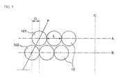
- FIG. 3 shows the above-described arrangement of the light illuminating means according to an exemplary embodiment of the present invention.
- a plurality of light illuminating means 10 are arranged in two rows, that is, in an A row and a B row.
- a line P connecting centers of the first and second light illuminating means may not be parallel to a line C formed in a direction perpendicular to the A and B rows.
- an illumination area of the first light illuminating means and an illumination area of the second light illuminating means may be overlapped to an extent Q in a direction perpendicular to the A and B rows.
- the amount of light radiated by the light source may be uniformly maintained.
- the degree of overlapping of one light illuminating means and another light illuminating means, for example, Q in FIG. 3 is not particularly limited.
- the degree of overlapping may be about 1/3 to 2/3 of a diameter of the light illuminating means, for example, about 1/3 to 2/3 of a diameter of L in FIG. 3 .
- the light illuminating apparatus may further include one or more light collecting plates configured to control the amount of light radiated from the light source.
- the light collecting plate may be included in the light illuminating apparatus so that light radiated from the light source is incident to and collected in the light collecting plate and then the collected light is radiated to the polarized ultraviolet light splitting element and the photo alignment mask.
- As the light collecting plate a well-known configuration formed to collect light radiated from the light source may be used.
- a lenticular lens layer may be used as the light collecting plate.
- FIG. 4 is a view showing a light illuminating apparatus according to an exemplary embodiment of the present invention.
- the light illuminating apparatus shown in FIG. 4 may include a light source 10, a light collecting plate 20, a polarized light plate 30, a mask 40, and a subject mounting device 60 for mounting a subject 50, which are sequentially arranged.
- light radiated from the light source 10 is incident to the light collecting plate 20 first, collected, and then is incident to the polarized light plate 30.
- Light incident to the polarized light plate 30 is converted to a linearly polarized light, becomes re-incident to the mask 40, and is guided by an opening to be radiated on a surface of the subject 50.
- a method of radiating light is provided.
- the method of radiating light according to the exemplary embodiment of the present invention may be performed using the above-described light illuminating apparatus.
- the method of radiating light may include mounting a subject on the subject mounting device, and irradiating the subject with light by the medium of the polarized ultraviolet light splitting element and the mask.
- the subject may be a photo alignment layer.
- the method of radiating light may be a method of preparing an aligned photo alignment layer.
- the aligned photo alignment layer may be fabricated by irradiating a photo alignment layer fixed on the subject mounting device with linearly polarized light, etc., by the medium of the polarized ultraviolet light splitting element and the mask, to align a photosensitive material included in the photo alignment layer in a predetermined direction.
- the type of the photo alignment layer applicable to the method of radiating light may not be particularly limited.
- Various types of photo alignment compounds having a photosensitive moiety and applicable for forming the photo alignment layer are well-known in the art, and those well-known photo alignment compounds may be used to form the photo alignment layer.
- the photo alignment compound may be, for example, a compound aligned by trans-cis photo-isomerization, a compound aligned by photolysis such as chain scission or photo-oxidation, a compound aligned by photo-crosslinking or photo-polymerization such as [2+2] cycloaddition, [4+4] cycloaddition, or photo-dimerization, a compound aligned by photo-Fries rearrangement, or a compound aligned by a ring opening/closure reaction.
- the compound aligned by trans-cis photo-isomerization may be, for example, an azo compound, such as a sulfonated diazo dye or an azo polymer, or stilbenes, and the compound aligned by photolysis may be, for example, cyclobutane-1,2,3,4-tetracarboxylic dianhydride, aromatic polysilane or polyester, a polystyrene or polyimide, etc.
- an azo compound such as a sulfonated diazo dye or an azo polymer, or stilbenes
- the compound aligned by photolysis may be, for example, cyclobutane-1,2,3,4-tetracarboxylic dianhydride, aromatic polysilane or polyester, a polystyrene or polyimide, etc.
- the compound aligned by photo-crosslinking or photo-polymerization may be a cinnamate compound, a coumarin compound, a cinnamamide compound, a tetrahydrophthalimide compound, a maleimide compound, a benzophenone compound, a diphenylacetylene compound, a compound having a chalconyl moiety as a photosensitive moiety (hereinafter, a chalcone compound) or a compound having an anthracenyl moiety (hereinafter, an anthracenyl compound), etc.
- the compound aligned by photo-Fries rearrangement may be an aromatic compound, such as a benzoate compound, a benzoamide compound, and a methacrylamidoaryl methacrylate compound.
- the compound aligned by a ring opening/closure reaction may be a [4+2] ⁇ -electronic system such as spiropyran compound, but is not limited thereto.
- the photo alignment layer may be formed by a well-known method in which the photo alignment compound is used.
- the photo alignment layer may be formed of the compound on a proper supporting substrate and applied to the method of radiating light while being transferred by a subject mounting device such as a roll.
- the photo alignment layer irradiated with light by the medium of the polarized ultraviolet light splitting element and the mask may be a first-aligned photo alignment layer.
- the first alignment may be achieved by irradiating the entire surface of the photo alignment layer with ultraviolet light linearly polarized in one direction by the polarized ultraviolet light splitting element before irradiating the photo alignment layer with light by the medium of the mask.
- the first-aligned photo alignment layer When light polarized in a direction different from the direction of the first alignment is radiated on the first-aligned photo alignment layer, the light is radiated only on an area of the photo alignment layer corresponding to the opening, and the photo alignment compound is rearranged. Thereby, a photo alignment layer in which the alignment direction of the photo alignment compound is patterned may be fabricated.
- the orientation of the photo alignment layer may be determined by the polarization direction of light radiated at the end. Accordingly, when the photo alignment layer is first-aligned in such a manner that ultraviolet light linearly polarized in one direction by the polarized ultraviolet light splitting element is radiated on the photo alignment layer, and then the first-aligned photo alignment layer is exposed to light linearly polarized in a direction different from the direction of the first alignment by the medium of the mask, the orientation of the photo alignment layer may be changed to a direction different from the direction of the first alignment only in a predetermined area on which the light is radiated. Accordingly, a pattern including at least a first alignment area having a first alignment orientation and a second alignment area having a second alignment orientation different from the first alignment orientation, or at least two types of alignment areas having different alignment orientations may be formed on the photo alignment layer.
- a polarization axis of the linearly polarized ultraviolet light during the first alignment may be perpendicular to a polarization axis of the linearly polarized ultraviolet light during a second alignment performed by the medium of the mask after the first alignment.
- the term “perpendicular” may refer to "substantially perpendicular”.
- the photo alignment layer fabricated by controlling polarization axes of light radiated during the first and second alignments may be, for example, used in an optical filter implementing three dimensional images.
- an optical filter may be fabricated by forming a liquid crystal layer on the above-described photo alignment layer.
- the method of preparing the liquid crystal layer may be, for example, but not limited thereto, formed by coating and aligning the photo alignment layer with a liquid crystal compound capable of being crosslinked or polymerized by light, and radiating light on the liquid crystal compound to be cross-linked or polymerized. Through the process, the liquid crystal compound layer is aligned and fixed along the orientation of the photo alignment layer, and a liquid crystal film including at least two areas having different alignment directions may be fabricated.
- the type of liquid crystal compound coated on the photo alignment layer is not particularly limited, and may be properly selected depending on the application of the optical filter.
- the liquid crystal compound may be aligned according to an alignment pattern of an alignment layer disposed therebelow and form a liquid crystal polymer layer having a ⁇ /4 phase difference by photo-crosslinking or photo-polymerization.
- ⁇ /4 phase difference may refer to a property by which an incident light is delayed by 1/4 of a wavelength of the incident light.
- an optical filter separates an incident light into a counterclockwise polarized light and clockwise polarized light
- Methods of depositing the liquid crystal compound, aligning the liquid crystal compound according to the alignment pattern of an alignment layer disposed therebelow, and crosslinking or polymerizing the aligned liquid crystal compound may not be particularly limited.
- the alignment may be executed by maintaining a liquid crystal layer at a proper temperature at which the liquid crystal compound has liquid crystallinity according to the type of the liquid crystal compound.
- the crosslinking or polymerization may be executed by irradiating a liquid crystal layer with light at a level at which a proper crosslinking or polymerizing is induced according to the type of the liquid crystal compound.
- a polarized ultraviolet light splitting element having an excellent splitting efficiency in a wide range of ultraviolet light and excellent durability can be provided.
- a quartz glass layer was ultrasonically cleaned in acetone and isopropyl alcohol (IPA) for 20 minutes to remove dust on a surface thereof.
- Ti and Ni were co-deposited on the quartz glass layer in an oxygen atmosphere using e-beam evaporation to form a metal composite oxide layer, which is represented by the following Chemical Formula 2, having a thickness of about 100 nm.
- the deposited layer was spin-coated with mr-8010r (manufactured by Micro Resist Technology GmbH) to have a thickness of 100 nm, and baked at the temperature of 95 °C for one minute.
- an imprint process was performed using an imprinting master. In the imprint process, the temperature of a press is about 160 °C.
- the metal composite oxide layer is maintained at 40 bar for 3 minutes, then cooled for two minutes, and then demolded at a temperature of 100 °C.
- the metal composite oxide layer is dry-etched using an ICP RIE apparatus.
- a resist used the imprint process is removed using acetone as an organic solvent, to fabricate a polarized ultraviolet light splitting element including a convex portion having a width W of about 70 nm and a pitch P of about 150 nm.
- a polarized ultraviolet light splitting element was fabricated using the same method as in Example 1.
- the polarized ultraviolet light splitting element includes a convex portion of a metal composite oxide layer, which is formed by codepositing Ti and Ni and represented by the following Chemical Formula 4.
- the polarized ultraviolet light splitting element has a height of about 100 nm, a width of about 70 nm, and a pitch of about 150 nm. [Chemical Formula 4] Ti x Cr y O 2
- a polarized ultraviolet light splitting element including a pattern formed by a TiO 2 convex portion was fabricated using the same method as in Example 1.
Landscapes
- Physics & Mathematics (AREA)
- General Physics & Mathematics (AREA)
- Optics & Photonics (AREA)
- Nonlinear Science (AREA)
- Engineering & Computer Science (AREA)
- General Engineering & Computer Science (AREA)
- High Energy & Nuclear Physics (AREA)
- Crystallography & Structural Chemistry (AREA)
- Chemical & Material Sciences (AREA)
- Liquid Crystal (AREA)
- Spectroscopy & Molecular Physics (AREA)
- Health & Medical Sciences (AREA)
- Mathematical Physics (AREA)
- Toxicology (AREA)
- Polarising Elements (AREA)
Applications Claiming Priority (2)
| Application Number | Priority Date | Filing Date | Title |
|---|---|---|---|
| KR20120095098 | 2012-08-29 | ||
| PCT/KR2013/007792 WO2014035170A1 (ko) | 2012-08-29 | 2013-08-29 | 편광 자외선 분리 소자 |
Publications (3)
| Publication Number | Publication Date |
|---|---|
| EP2891908A1 true EP2891908A1 (de) | 2015-07-08 |
| EP2891908A4 EP2891908A4 (de) | 2016-08-24 |
| EP2891908B1 EP2891908B1 (de) | 2022-10-26 |
Family
ID=50642401
Family Applications (1)
| Application Number | Title | Priority Date | Filing Date |
|---|---|---|---|
| EP13833108.7A Active EP2891908B1 (de) | 2012-08-29 | 2013-08-29 | Teilungselement für polarisiertes uv-licht |
Country Status (6)
| Country | Link |
|---|---|
| US (1) | US9442303B2 (de) |
| EP (1) | EP2891908B1 (de) |
| JP (2) | JP2015528589A (de) |
| KR (1) | KR101722808B1 (de) |
| CN (1) | CN104755971B (de) |
| WO (1) | WO2014035170A1 (de) |
Families Citing this family (3)
| Publication number | Priority date | Publication date | Assignee | Title |
|---|---|---|---|---|
| KR101729683B1 (ko) * | 2015-09-16 | 2017-04-25 | 한국기계연구원 | 선격자 편광자의 제조 방법 |
| CN115443426B (zh) * | 2020-04-07 | 2025-01-21 | 斯纳普公司 | 光学装置 |
| CN114371151B (zh) * | 2020-10-15 | 2024-04-19 | 深圳莱宝高科技股份有限公司 | 一种透过率测试方法 |
Family Cites Families (34)
| Publication number | Priority date | Publication date | Assignee | Title |
|---|---|---|---|---|
| US5541057A (en) * | 1989-09-18 | 1996-07-30 | Biostar, Inc. | Methods for detection of an analyte |
| JP3168765B2 (ja) * | 1993-04-01 | 2001-05-21 | 松下電器産業株式会社 | 偏光装置および該偏光装置を用いた投写型表示装置 |
| JP3168770B2 (ja) * | 1993-06-03 | 2001-05-21 | 松下電器産業株式会社 | 偏光装置および該偏光装置を用いた投写型表示装置 |
| JPH0961627A (ja) | 1995-08-25 | 1997-03-07 | Sankyo Seiki Mfg Co Ltd | 偏光分離素子 |
| JP3817970B2 (ja) * | 1999-05-31 | 2006-09-06 | ウシオ電機株式会社 | 偏光ビームスプリッタおよびそれを用いた液晶表示素子の配向膜光配向用偏光光照射装置 |
| US6243199B1 (en) | 1999-09-07 | 2001-06-05 | Moxtek | Broad band wire grid polarizing beam splitter for use in the visible wavelength region |
| JP3948192B2 (ja) * | 1999-11-10 | 2007-07-25 | 凸版印刷株式会社 | ポリエステル系樹脂組成物、ボトル、フィルムおよびトレー |
| JP2001147320A (ja) * | 1999-11-19 | 2001-05-29 | Mitsubishi Polyester Film Copp | 偏光子保護フィルム |
| JP2002055226A (ja) * | 2000-08-07 | 2002-02-20 | Nippon Sheet Glass Co Ltd | 偏光素子及びその製造方法 |
| JP2002189301A (ja) * | 2000-12-22 | 2002-07-05 | Ushio Inc | 光配向用偏光光照射装置 |
| US7146064B2 (en) * | 2001-12-21 | 2006-12-05 | Gsi Group Corporation | System and method for producing optical circuits |
| KR100457222B1 (ko) | 2002-06-25 | 2004-11-16 | 동부전자 주식회사 | 고전압 소자의 제조방법 |
| JP4216220B2 (ja) | 2004-04-12 | 2009-01-28 | 株式会社 日立ディスプレイズ | 液晶表示素子の製造方法 |
| JP2006011296A (ja) * | 2004-06-29 | 2006-01-12 | Toshiba Corp | 偏光素子、偏光素子の製造方法、及び露光装置の評価方法 |
| US7961393B2 (en) * | 2004-12-06 | 2011-06-14 | Moxtek, Inc. | Selectively absorptive wire-grid polarizer |
| JP4275692B2 (ja) * | 2005-10-17 | 2009-06-10 | 旭化成株式会社 | ワイヤグリッド偏光板及びそれを用いた液晶表示装置 |
| JP4275691B2 (ja) * | 2005-10-17 | 2009-06-10 | 旭化成株式会社 | ワイヤグリッド偏光板の製造方法 |
| US7894019B2 (en) * | 2005-10-17 | 2011-02-22 | Asahi Kasei Kabushiki Kaisha | Wire grid polarizer and liquid crystal display device using the same |
| CN1952700B (zh) | 2005-10-17 | 2010-06-09 | 旭化成电子材料株式会社 | 线栅偏振片及其制造方法 |
| JP5933910B2 (ja) * | 2006-08-15 | 2016-06-15 | ポラリゼーション ソリューションズ エルエルシー | 偏光子薄膜及びこの製作方法 |
| JP4708287B2 (ja) | 2006-08-25 | 2011-06-22 | 富士フイルム株式会社 | 光学フィルムの製造方法、光学フィルム、偏光板、転写材料、液晶表示装置、及び偏光紫外線露光装置 |
| US8755113B2 (en) | 2006-08-31 | 2014-06-17 | Moxtek, Inc. | Durable, inorganic, absorptive, ultra-violet, grid polarizer |
| JP4795214B2 (ja) * | 2006-12-07 | 2011-10-19 | チェイル インダストリーズ インコーポレイテッド | ワイヤーグリッド偏光子及びその製造方法 |
| JP4142092B2 (ja) * | 2006-12-13 | 2008-08-27 | 財団法人川村理化学研究所 | ドーピング酸化チタンの製造方法、ドーピング酸化チタン及びこれを用いる可視光応答型光触媒 |
| TWI431338B (zh) * | 2007-01-12 | 2014-03-21 | Toray Industries | 偏光板及使用它之液晶顯示裝置 |
| JP5274006B2 (ja) | 2007-12-26 | 2013-08-28 | チェイル インダストリーズ インコーポレイテッド | ワイヤグリッド偏光子およびその製造方法 |
| JP4955594B2 (ja) * | 2008-03-17 | 2012-06-20 | 富士フイルム株式会社 | 光軸方向および位相差量がパターニングされた光学材料 |
| JP4968165B2 (ja) | 2008-04-24 | 2012-07-04 | ウシオ電機株式会社 | 光配向用偏光光照射装置 |
| US8941920B2 (en) * | 2008-07-28 | 2015-01-27 | Canon Kabushiki Kaisha | Method of producing optical element and optical element |
| KR101725342B1 (ko) | 2009-10-12 | 2017-04-11 | 삼성디스플레이 주식회사 | 광배향용 마스크, 이를 이용한 광배향 방법 및 액정 표시 장치 |
| US20110256385A1 (en) * | 2010-04-15 | 2011-10-20 | Seiko Epson Corporation | Bonding film-attached substrate and bonding film-attached substrate manufacturing method |
| JP5516224B2 (ja) * | 2010-08-20 | 2014-06-11 | 大日本印刷株式会社 | パターン形成方法とナノインプリントモールドおよびナノインプリント用転写基材 |
| KR20120069014A (ko) * | 2010-11-12 | 2012-06-28 | 동우 화인켐 주식회사 | 투명 격벽들이 구비된 마스크 및 이를 포함하는 노광 장치 |
| KR20120072201A (ko) | 2010-12-23 | 2012-07-03 | 한국전자통신연구원 | 편광소자의 제조방법 |
-
2013
- 2013-08-29 EP EP13833108.7A patent/EP2891908B1/de active Active
- 2013-08-29 KR KR1020130103320A patent/KR101722808B1/ko active Active
- 2013-08-29 CN CN201380055072.XA patent/CN104755971B/zh active Active
- 2013-08-29 US US14/424,915 patent/US9442303B2/en active Active
- 2013-08-29 JP JP2015529680A patent/JP2015528589A/ja active Pending
- 2013-08-29 WO PCT/KR2013/007792 patent/WO2014035170A1/ko not_active Ceased
-
2017
- 2017-08-23 JP JP2017160168A patent/JP6402390B2/ja active Active
Also Published As
| Publication number | Publication date |
|---|---|
| EP2891908A4 (de) | 2016-08-24 |
| EP2891908B1 (de) | 2022-10-26 |
| CN104755971A (zh) | 2015-07-01 |
| WO2014035170A1 (ko) | 2014-03-06 |
| JP2018022161A (ja) | 2018-02-08 |
| JP2015528589A (ja) | 2015-09-28 |
| US20150219918A1 (en) | 2015-08-06 |
| CN104755971B (zh) | 2017-09-29 |
| JP6402390B2 (ja) | 2018-10-10 |
| KR20140029305A (ko) | 2014-03-10 |
| US9442303B2 (en) | 2016-09-13 |
| KR101722808B1 (ko) | 2017-04-04 |
Similar Documents
| Publication | Publication Date | Title |
|---|---|---|
| KR101377296B1 (ko) | 편광 분리 소자의 제조방법 | |
| KR101473062B1 (ko) | 마스크 | |
| US9541693B2 (en) | Polarized light splitting element | |
| US20070242187A1 (en) | Wire grid polarizer and liquid crystal display device using the polarizer | |
| EP2790044B1 (de) | Polarisationstrennungselement | |
| EP2891908B1 (de) | Teilungselement für polarisiertes uv-licht | |
| EP2891909B1 (de) | Verfahren zur herstellung eines elements zum aufspalten von polarisiertem licht | |
| KR100809835B1 (ko) | 아크릴로일 기를 가지는 아조계 유기 고분자 |
Legal Events
| Date | Code | Title | Description |
|---|---|---|---|
| PUAI | Public reference made under article 153(3) epc to a published international application that has entered the european phase |
Free format text: ORIGINAL CODE: 0009012 |
|
| 17P | Request for examination filed |
Effective date: 20150225 |
|
| AK | Designated contracting states |
Kind code of ref document: A1 Designated state(s): AL AT BE BG CH CY CZ DE DK EE ES FI FR GB GR HR HU IE IS IT LI LT LU LV MC MK MT NL NO PL PT RO RS SE SI SK SM TR |
|
| AX | Request for extension of the european patent |
Extension state: BA ME |
|
| DAX | Request for extension of the european patent (deleted) | ||
| RIC1 | Information provided on ipc code assigned before grant |
Ipc: G02B 5/20 20060101ALI20160316BHEP Ipc: G02B 5/30 20060101AFI20160316BHEP Ipc: G02F 1/13 20060101ALI20160316BHEP |
|
| RA4 | Supplementary search report drawn up and despatched (corrected) |
Effective date: 20160721 |
|
| RIC1 | Information provided on ipc code assigned before grant |
Ipc: G02B 5/30 20060101AFI20160715BHEP Ipc: G02B 5/20 20060101ALI20160715BHEP Ipc: G02F 1/13 20060101ALI20160715BHEP |
|
| STAA | Information on the status of an ep patent application or granted ep patent |
Free format text: STATUS: EXAMINATION IS IN PROGRESS |
|
| 17Q | First examination report despatched |
Effective date: 20181109 |
|
| GRAP | Despatch of communication of intention to grant a patent |
Free format text: ORIGINAL CODE: EPIDOSNIGR1 |
|
| STAA | Information on the status of an ep patent application or granted ep patent |
Free format text: STATUS: GRANT OF PATENT IS INTENDED |
|
| INTG | Intention to grant announced |
Effective date: 20220818 |
|
| GRAS | Grant fee paid |
Free format text: ORIGINAL CODE: EPIDOSNIGR3 |
|
| GRAA | (expected) grant |
Free format text: ORIGINAL CODE: 0009210 |
|
| STAA | Information on the status of an ep patent application or granted ep patent |
Free format text: STATUS: THE PATENT HAS BEEN GRANTED |
|
| AK | Designated contracting states |
Kind code of ref document: B1 Designated state(s): AL AT BE BG CH CY CZ DE DK EE ES FI FR GB GR HR HU IE IS IT LI LT LU LV MC MK MT NL NO PL PT RO RS SE SI SK SM TR |
|
| REG | Reference to a national code |
Ref country code: GB Ref legal event code: FG4D |
|
| REG | Reference to a national code |
Ref country code: CH Ref legal event code: EP |
|
| REG | Reference to a national code |
Ref country code: AT Ref legal event code: REF Ref document number: 1527425 Country of ref document: AT Kind code of ref document: T Effective date: 20221115 |
|
| REG | Reference to a national code |
Ref country code: DE Ref legal event code: R096 Ref document number: 602013082761 Country of ref document: DE |
|
| REG | Reference to a national code |
Ref country code: IE Ref legal event code: FG4D |
|
| REG | Reference to a national code |
Ref country code: LT Ref legal event code: MG9D |
|
| REG | Reference to a national code |
Ref country code: NL Ref legal event code: MP Effective date: 20221026 |
|
| REG | Reference to a national code |
Ref country code: AT Ref legal event code: MK05 Ref document number: 1527425 Country of ref document: AT Kind code of ref document: T Effective date: 20221026 |
|
| PG25 | Lapsed in a contracting state [announced via postgrant information from national office to epo] |
Ref country code: NL Free format text: LAPSE BECAUSE OF FAILURE TO SUBMIT A TRANSLATION OF THE DESCRIPTION OR TO PAY THE FEE WITHIN THE PRESCRIBED TIME-LIMIT Effective date: 20221026 |
|
| PG25 | Lapsed in a contracting state [announced via postgrant information from national office to epo] |
Ref country code: SE Free format text: LAPSE BECAUSE OF FAILURE TO SUBMIT A TRANSLATION OF THE DESCRIPTION OR TO PAY THE FEE WITHIN THE PRESCRIBED TIME-LIMIT Effective date: 20221026 Ref country code: PT Free format text: LAPSE BECAUSE OF FAILURE TO SUBMIT A TRANSLATION OF THE DESCRIPTION OR TO PAY THE FEE WITHIN THE PRESCRIBED TIME-LIMIT Effective date: 20230227 Ref country code: NO Free format text: LAPSE BECAUSE OF FAILURE TO SUBMIT A TRANSLATION OF THE DESCRIPTION OR TO PAY THE FEE WITHIN THE PRESCRIBED TIME-LIMIT Effective date: 20230126 Ref country code: LT Free format text: LAPSE BECAUSE OF FAILURE TO SUBMIT A TRANSLATION OF THE DESCRIPTION OR TO PAY THE FEE WITHIN THE PRESCRIBED TIME-LIMIT Effective date: 20221026 Ref country code: FI Free format text: LAPSE BECAUSE OF FAILURE TO SUBMIT A TRANSLATION OF THE DESCRIPTION OR TO PAY THE FEE WITHIN THE PRESCRIBED TIME-LIMIT Effective date: 20221026 Ref country code: ES Free format text: LAPSE BECAUSE OF FAILURE TO SUBMIT A TRANSLATION OF THE DESCRIPTION OR TO PAY THE FEE WITHIN THE PRESCRIBED TIME-LIMIT Effective date: 20221026 Ref country code: AT Free format text: LAPSE BECAUSE OF FAILURE TO SUBMIT A TRANSLATION OF THE DESCRIPTION OR TO PAY THE FEE WITHIN THE PRESCRIBED TIME-LIMIT Effective date: 20221026 |
|
| PG25 | Lapsed in a contracting state [announced via postgrant information from national office to epo] |
Ref country code: RS Free format text: LAPSE BECAUSE OF FAILURE TO SUBMIT A TRANSLATION OF THE DESCRIPTION OR TO PAY THE FEE WITHIN THE PRESCRIBED TIME-LIMIT Effective date: 20221026 Ref country code: PL Free format text: LAPSE BECAUSE OF FAILURE TO SUBMIT A TRANSLATION OF THE DESCRIPTION OR TO PAY THE FEE WITHIN THE PRESCRIBED TIME-LIMIT Effective date: 20221026 Ref country code: LV Free format text: LAPSE BECAUSE OF FAILURE TO SUBMIT A TRANSLATION OF THE DESCRIPTION OR TO PAY THE FEE WITHIN THE PRESCRIBED TIME-LIMIT Effective date: 20221026 Ref country code: IS Free format text: LAPSE BECAUSE OF FAILURE TO SUBMIT A TRANSLATION OF THE DESCRIPTION OR TO PAY THE FEE WITHIN THE PRESCRIBED TIME-LIMIT Effective date: 20230226 Ref country code: HR Free format text: LAPSE BECAUSE OF FAILURE TO SUBMIT A TRANSLATION OF THE DESCRIPTION OR TO PAY THE FEE WITHIN THE PRESCRIBED TIME-LIMIT Effective date: 20221026 Ref country code: GR Free format text: LAPSE BECAUSE OF FAILURE TO SUBMIT A TRANSLATION OF THE DESCRIPTION OR TO PAY THE FEE WITHIN THE PRESCRIBED TIME-LIMIT Effective date: 20230127 |
|
| REG | Reference to a national code |
Ref country code: DE Ref legal event code: R097 Ref document number: 602013082761 Country of ref document: DE |
|
| PG25 | Lapsed in a contracting state [announced via postgrant information from national office to epo] |
Ref country code: SM Free format text: LAPSE BECAUSE OF FAILURE TO SUBMIT A TRANSLATION OF THE DESCRIPTION OR TO PAY THE FEE WITHIN THE PRESCRIBED TIME-LIMIT Effective date: 20221026 Ref country code: RO Free format text: LAPSE BECAUSE OF FAILURE TO SUBMIT A TRANSLATION OF THE DESCRIPTION OR TO PAY THE FEE WITHIN THE PRESCRIBED TIME-LIMIT Effective date: 20221026 Ref country code: EE Free format text: LAPSE BECAUSE OF FAILURE TO SUBMIT A TRANSLATION OF THE DESCRIPTION OR TO PAY THE FEE WITHIN THE PRESCRIBED TIME-LIMIT Effective date: 20221026 Ref country code: DK Free format text: LAPSE BECAUSE OF FAILURE TO SUBMIT A TRANSLATION OF THE DESCRIPTION OR TO PAY THE FEE WITHIN THE PRESCRIBED TIME-LIMIT Effective date: 20221026 Ref country code: CZ Free format text: LAPSE BECAUSE OF FAILURE TO SUBMIT A TRANSLATION OF THE DESCRIPTION OR TO PAY THE FEE WITHIN THE PRESCRIBED TIME-LIMIT Effective date: 20221026 |
|
| PG25 | Lapsed in a contracting state [announced via postgrant information from national office to epo] |
Ref country code: SK Free format text: LAPSE BECAUSE OF FAILURE TO SUBMIT A TRANSLATION OF THE DESCRIPTION OR TO PAY THE FEE WITHIN THE PRESCRIBED TIME-LIMIT Effective date: 20221026 Ref country code: AL Free format text: LAPSE BECAUSE OF FAILURE TO SUBMIT A TRANSLATION OF THE DESCRIPTION OR TO PAY THE FEE WITHIN THE PRESCRIBED TIME-LIMIT Effective date: 20221026 |
|
| PLBE | No opposition filed within time limit |
Free format text: ORIGINAL CODE: 0009261 |
|
| STAA | Information on the status of an ep patent application or granted ep patent |
Free format text: STATUS: NO OPPOSITION FILED WITHIN TIME LIMIT |
|
| 26N | No opposition filed |
Effective date: 20230727 |
|
| PG25 | Lapsed in a contracting state [announced via postgrant information from national office to epo] |
Ref country code: SI Free format text: LAPSE BECAUSE OF FAILURE TO SUBMIT A TRANSLATION OF THE DESCRIPTION OR TO PAY THE FEE WITHIN THE PRESCRIBED TIME-LIMIT Effective date: 20221026 |
|
| PG25 | Lapsed in a contracting state [announced via postgrant information from national office to epo] |
Ref country code: MC Free format text: LAPSE BECAUSE OF FAILURE TO SUBMIT A TRANSLATION OF THE DESCRIPTION OR TO PAY THE FEE WITHIN THE PRESCRIBED TIME-LIMIT Effective date: 20221026 |
|
| REG | Reference to a national code |
Ref country code: CH Ref legal event code: PL |
|
| PG25 | Lapsed in a contracting state [announced via postgrant information from national office to epo] |
Ref country code: MC Free format text: LAPSE BECAUSE OF FAILURE TO SUBMIT A TRANSLATION OF THE DESCRIPTION OR TO PAY THE FEE WITHIN THE PRESCRIBED TIME-LIMIT Effective date: 20221026 |
|
| PG25 | Lapsed in a contracting state [announced via postgrant information from national office to epo] |
Ref country code: LU Free format text: LAPSE BECAUSE OF NON-PAYMENT OF DUE FEES Effective date: 20230829 |
|
| PG25 | Lapsed in a contracting state [announced via postgrant information from national office to epo] |
Ref country code: LU Free format text: LAPSE BECAUSE OF NON-PAYMENT OF DUE FEES Effective date: 20230829 Ref country code: CH Free format text: LAPSE BECAUSE OF NON-PAYMENT OF DUE FEES Effective date: 20230831 |
|
| REG | Reference to a national code |
Ref country code: BE Ref legal event code: MM Effective date: 20230831 |
|
| REG | Reference to a national code |
Ref country code: IE Ref legal event code: MM4A |
|
| PG25 | Lapsed in a contracting state [announced via postgrant information from national office to epo] |
Ref country code: IT Free format text: LAPSE BECAUSE OF FAILURE TO SUBMIT A TRANSLATION OF THE DESCRIPTION OR TO PAY THE FEE WITHIN THE PRESCRIBED TIME-LIMIT Effective date: 20221026 |
|
| PG25 | Lapsed in a contracting state [announced via postgrant information from national office to epo] |
Ref country code: IE Free format text: LAPSE BECAUSE OF NON-PAYMENT OF DUE FEES Effective date: 20230829 |
|
| PG25 | Lapsed in a contracting state [announced via postgrant information from national office to epo] |
Ref country code: IE Free format text: LAPSE BECAUSE OF NON-PAYMENT OF DUE FEES Effective date: 20230829 |
|
| PG25 | Lapsed in a contracting state [announced via postgrant information from national office to epo] |
Ref country code: BE Free format text: LAPSE BECAUSE OF NON-PAYMENT OF DUE FEES Effective date: 20230831 |
|
| PG25 | Lapsed in a contracting state [announced via postgrant information from national office to epo] |
Ref country code: BG Free format text: LAPSE BECAUSE OF FAILURE TO SUBMIT A TRANSLATION OF THE DESCRIPTION OR TO PAY THE FEE WITHIN THE PRESCRIBED TIME-LIMIT Effective date: 20221026 |
|
| PG25 | Lapsed in a contracting state [announced via postgrant information from national office to epo] |
Ref country code: BG Free format text: LAPSE BECAUSE OF FAILURE TO SUBMIT A TRANSLATION OF THE DESCRIPTION OR TO PAY THE FEE WITHIN THE PRESCRIBED TIME-LIMIT Effective date: 20221026 |
|
| PG25 | Lapsed in a contracting state [announced via postgrant information from national office to epo] |
Ref country code: CY Free format text: LAPSE BECAUSE OF FAILURE TO SUBMIT A TRANSLATION OF THE DESCRIPTION OR TO PAY THE FEE WITHIN THE PRESCRIBED TIME-LIMIT; INVALID AB INITIO Effective date: 20130829 |
|
| PG25 | Lapsed in a contracting state [announced via postgrant information from national office to epo] |
Ref country code: HU Free format text: LAPSE BECAUSE OF FAILURE TO SUBMIT A TRANSLATION OF THE DESCRIPTION OR TO PAY THE FEE WITHIN THE PRESCRIBED TIME-LIMIT; INVALID AB INITIO Effective date: 20130829 |
|
| PGFP | Annual fee paid to national office [announced via postgrant information from national office to epo] |
Ref country code: DE Payment date: 20250721 Year of fee payment: 13 |
|
| PGFP | Annual fee paid to national office [announced via postgrant information from national office to epo] |
Ref country code: GB Payment date: 20250722 Year of fee payment: 13 |
|
| PGFP | Annual fee paid to national office [announced via postgrant information from national office to epo] |
Ref country code: FR Payment date: 20250725 Year of fee payment: 13 |
|
| PG25 | Lapsed in a contracting state [announced via postgrant information from national office to epo] |
Ref country code: TR Free format text: LAPSE BECAUSE OF FAILURE TO SUBMIT A TRANSLATION OF THE DESCRIPTION OR TO PAY THE FEE WITHIN THE PRESCRIBED TIME-LIMIT Effective date: 20221026 |