EP2889869A1 - Display device - Google Patents
Display device Download PDFInfo
- Publication number
- EP2889869A1 EP2889869A1 EP14169208.7A EP14169208A EP2889869A1 EP 2889869 A1 EP2889869 A1 EP 2889869A1 EP 14169208 A EP14169208 A EP 14169208A EP 2889869 A1 EP2889869 A1 EP 2889869A1
- Authority
- EP
- European Patent Office
- Prior art keywords
- data
- subpixels
- subpixel
- color
- lines
- Prior art date
- Legal status (The legal status is an assumption and is not a legal conclusion. Google has not performed a legal analysis and makes no representation as to the accuracy of the status listed.)
- Ceased
Links
Images





Classifications
-
- G—PHYSICS
- G09—EDUCATION; CRYPTOGRAPHY; DISPLAY; ADVERTISING; SEALS
- G09G—ARRANGEMENTS OR CIRCUITS FOR CONTROL OF INDICATING DEVICES USING STATIC MEANS TO PRESENT VARIABLE INFORMATION
- G09G3/00—Control arrangements or circuits, of interest only in connection with visual indicators other than cathode-ray tubes
- G09G3/20—Control arrangements or circuits, of interest only in connection with visual indicators other than cathode-ray tubes for presentation of an assembly of a number of characters, e.g. a page, by composing the assembly by combination of individual elements arranged in a matrix no fixed position being assigned to or needed to be assigned to the individual characters or partial characters
- G09G3/34—Control arrangements or circuits, of interest only in connection with visual indicators other than cathode-ray tubes for presentation of an assembly of a number of characters, e.g. a page, by composing the assembly by combination of individual elements arranged in a matrix no fixed position being assigned to or needed to be assigned to the individual characters or partial characters by control of light from an independent source
- G09G3/36—Control arrangements or circuits, of interest only in connection with visual indicators other than cathode-ray tubes for presentation of an assembly of a number of characters, e.g. a page, by composing the assembly by combination of individual elements arranged in a matrix no fixed position being assigned to or needed to be assigned to the individual characters or partial characters by control of light from an independent source using liquid crystals
-
- G—PHYSICS
- G09—EDUCATION; CRYPTOGRAPHY; DISPLAY; ADVERTISING; SEALS
- G09G—ARRANGEMENTS OR CIRCUITS FOR CONTROL OF INDICATING DEVICES USING STATIC MEANS TO PRESENT VARIABLE INFORMATION
- G09G3/00—Control arrangements or circuits, of interest only in connection with visual indicators other than cathode-ray tubes
- G09G3/20—Control arrangements or circuits, of interest only in connection with visual indicators other than cathode-ray tubes for presentation of an assembly of a number of characters, e.g. a page, by composing the assembly by combination of individual elements arranged in a matrix no fixed position being assigned to or needed to be assigned to the individual characters or partial characters
- G09G3/34—Control arrangements or circuits, of interest only in connection with visual indicators other than cathode-ray tubes for presentation of an assembly of a number of characters, e.g. a page, by composing the assembly by combination of individual elements arranged in a matrix no fixed position being assigned to or needed to be assigned to the individual characters or partial characters by control of light from an independent source
- G09G3/36—Control arrangements or circuits, of interest only in connection with visual indicators other than cathode-ray tubes for presentation of an assembly of a number of characters, e.g. a page, by composing the assembly by combination of individual elements arranged in a matrix no fixed position being assigned to or needed to be assigned to the individual characters or partial characters by control of light from an independent source using liquid crystals
- G09G3/3607—Control arrangements or circuits, of interest only in connection with visual indicators other than cathode-ray tubes for presentation of an assembly of a number of characters, e.g. a page, by composing the assembly by combination of individual elements arranged in a matrix no fixed position being assigned to or needed to be assigned to the individual characters or partial characters by control of light from an independent source using liquid crystals for displaying colours or for displaying grey scales with a specific pixel layout, e.g. using sub-pixels
-
- G—PHYSICS
- G09—EDUCATION; CRYPTOGRAPHY; DISPLAY; ADVERTISING; SEALS
- G09G—ARRANGEMENTS OR CIRCUITS FOR CONTROL OF INDICATING DEVICES USING STATIC MEANS TO PRESENT VARIABLE INFORMATION
- G09G3/00—Control arrangements or circuits, of interest only in connection with visual indicators other than cathode-ray tubes
- G09G3/20—Control arrangements or circuits, of interest only in connection with visual indicators other than cathode-ray tubes for presentation of an assembly of a number of characters, e.g. a page, by composing the assembly by combination of individual elements arranged in a matrix no fixed position being assigned to or needed to be assigned to the individual characters or partial characters
-
- G—PHYSICS
- G09—EDUCATION; CRYPTOGRAPHY; DISPLAY; ADVERTISING; SEALS
- G09G—ARRANGEMENTS OR CIRCUITS FOR CONTROL OF INDICATING DEVICES USING STATIC MEANS TO PRESENT VARIABLE INFORMATION
- G09G3/00—Control arrangements or circuits, of interest only in connection with visual indicators other than cathode-ray tubes
- G09G3/20—Control arrangements or circuits, of interest only in connection with visual indicators other than cathode-ray tubes for presentation of an assembly of a number of characters, e.g. a page, by composing the assembly by combination of individual elements arranged in a matrix no fixed position being assigned to or needed to be assigned to the individual characters or partial characters
- G09G3/34—Control arrangements or circuits, of interest only in connection with visual indicators other than cathode-ray tubes for presentation of an assembly of a number of characters, e.g. a page, by composing the assembly by combination of individual elements arranged in a matrix no fixed position being assigned to or needed to be assigned to the individual characters or partial characters by control of light from an independent source
- G09G3/36—Control arrangements or circuits, of interest only in connection with visual indicators other than cathode-ray tubes for presentation of an assembly of a number of characters, e.g. a page, by composing the assembly by combination of individual elements arranged in a matrix no fixed position being assigned to or needed to be assigned to the individual characters or partial characters by control of light from an independent source using liquid crystals
- G09G3/3611—Control of matrices with row and column drivers
- G09G3/3614—Control of polarity reversal in general
-
- G—PHYSICS
- G09—EDUCATION; CRYPTOGRAPHY; DISPLAY; ADVERTISING; SEALS
- G09G—ARRANGEMENTS OR CIRCUITS FOR CONTROL OF INDICATING DEVICES USING STATIC MEANS TO PRESENT VARIABLE INFORMATION
- G09G2300/00—Aspects of the constitution of display devices
- G09G2300/04—Structural and physical details of display devices
- G09G2300/0421—Structural details of the set of electrodes
- G09G2300/0426—Layout of electrodes and connections
-
- G—PHYSICS
- G09—EDUCATION; CRYPTOGRAPHY; DISPLAY; ADVERTISING; SEALS
- G09G—ARRANGEMENTS OR CIRCUITS FOR CONTROL OF INDICATING DEVICES USING STATIC MEANS TO PRESENT VARIABLE INFORMATION
- G09G2300/00—Aspects of the constitution of display devices
- G09G2300/04—Structural and physical details of display devices
- G09G2300/0439—Pixel structures
-
- G—PHYSICS
- G09—EDUCATION; CRYPTOGRAPHY; DISPLAY; ADVERTISING; SEALS
- G09G—ARRANGEMENTS OR CIRCUITS FOR CONTROL OF INDICATING DEVICES USING STATIC MEANS TO PRESENT VARIABLE INFORMATION
- G09G2300/00—Aspects of the constitution of display devices
- G09G2300/04—Structural and physical details of display devices
- G09G2300/0439—Pixel structures
- G09G2300/0452—Details of colour pixel setup, e.g. pixel composed of a red, a blue and two green components
-
- G—PHYSICS
- G09—EDUCATION; CRYPTOGRAPHY; DISPLAY; ADVERTISING; SEALS
- G09G—ARRANGEMENTS OR CIRCUITS FOR CONTROL OF INDICATING DEVICES USING STATIC MEANS TO PRESENT VARIABLE INFORMATION
- G09G2310/00—Command of the display device
- G09G2310/02—Addressing, scanning or driving the display screen or processing steps related thereto
- G09G2310/0264—Details of driving circuits
- G09G2310/0297—Special arrangements with multiplexing or demultiplexing of display data in the drivers for data electrodes, in a pre-processing circuitry delivering display data to said drivers or in the matrix panel, e.g. multiplexing plural data signals to one D/A converter or demultiplexing the D/A converter output to multiple columns
-
- G—PHYSICS
- G09—EDUCATION; CRYPTOGRAPHY; DISPLAY; ADVERTISING; SEALS
- G09G—ARRANGEMENTS OR CIRCUITS FOR CONTROL OF INDICATING DEVICES USING STATIC MEANS TO PRESENT VARIABLE INFORMATION
- G09G2320/00—Control of display operating conditions
- G09G2320/02—Improving the quality of display appearance
- G09G2320/0242—Compensation of deficiencies in the appearance of colours
-
- G—PHYSICS
- G09—EDUCATION; CRYPTOGRAPHY; DISPLAY; ADVERTISING; SEALS
- G09G—ARRANGEMENTS OR CIRCUITS FOR CONTROL OF INDICATING DEVICES USING STATIC MEANS TO PRESENT VARIABLE INFORMATION
- G09G2320/00—Control of display operating conditions
- G09G2320/02—Improving the quality of display appearance
- G09G2320/0247—Flicker reduction other than flicker reduction circuits used for single beam cathode-ray tubes
Definitions
- Embodiments of the invention relate to a display device, in which each pixel is divided into four color subpixels.
- Various flat panel displays such as a liquid crystal display (LCD), a plasma display panel (PDP), an organic light emitting display, and an electrophoresis display (EPD), have been developed.
- the liquid crystal display displays an image by controlling an electric field applied to liquid crystal molecules based on a data voltage.
- An active matrix liquid crystal display includes a thin film transistor (TFT) in each pixel.
- the pixels of the liquid crystal display may be divided into red (R) subpixels, green (G) subpixels, blue (B) subpixels, and white (W) subpixels, so as to represent colors and increase a luminance.
- the display device in which the pixels are divided into the RGBW subpixels, is referred to as an RGBW type display device.
- the liquid crystal display includes a liquid crystal display panel, a backlight unit providing light to the liquid crystal display panel, source driver integrated circuits (ICs) for supplying a data voltage to data lines of the liquid crystal display panel, gate driver ICs for supplying a gate pulse (or scan pulse) to gate lines (or scan lines) of the liquid crystal display panel, a control circuit for controlling the source driver ICs and the gate driver ICs, a light source driving circuit for driving light sources of the backlight unit, etc.
- source driver integrated circuits ICs
- gate driver ICs for supplying a gate pulse (or scan pulse) to gate lines (or scan lines) of the liquid crystal display panel
- control circuit for controlling the source driver ICs and the gate driver ICs
- a light source driving circuit for driving light sources of the backlight unit, etc.
- polarities of the data voltages charged to adjacent subpixels are opposite to each other and are periodically inverted, so as to reduce DC image sticking and prevent the degradation of liquid crystals.
- a horizontal and vertical 1-dot inversion scheme or a horizontal 1-dot and vertical 2-dot inversion scheme has been applied to most of the liquid crystal displays.
- the 1-dot means one subpixel.
- a charge amount of subpixels of each color may vary depending on a relationship between data of an input image and a polarity pattern of the pixels.
- a line noise of a longitudinal line shape and color distortion may appear in an image displayed on a pixel array due to the color arrangement of the subpixels.
- Embodiments of the invention provide a liquid crystal display, in which each pixels is divided into four color subpixels, capable of improving the display quality.
- a display panel (10) comprising a plurality of data lines (D1 to Dm) and a plurality of gate lines (G1 to Gn) intersecting the data lines (D1 to Dm); a pixel array comprising a plurality of pixels arranged in a matrix form and coupled to the data lines (D1 to Dm) and gate lines (G1 to Gn), each pixel being divided into a first subpixel having a first color (R), a second subpixel having a second color (G), a third subpixel having a third color (B), and a fourth subpixel having a fourth color (W), wherein two adjacent subpixels in a horizontal line of the pixel array share a data line of the plurality of data lines (D1 to Dm); wherein the subpixels of the plurality of pixels of the pixel array are arranged such that subpixels having the same color and arranged in four adjacent horizontal lines of the pixel array form a hexagonal shape.
- a display device comprising the display panel; a display panel driving circuit comprising a timing controller, a data driver (12) coupled to the data lines (D1 to Dm) and configured to provide data voltages to the data lines, and a gate driver (14) coupled to the gate lines (G1 to Gn) and configured to provide scan pulses to the gate lines.
- a display device may be implemented as a flat panel display capable of representing colors, such as a liquid crystal display (LCD), a plasma display panel (PDP), and an organic light emitting display.
- LCD liquid crystal display
- PDP plasma display panel
- organic light emitting display an organic light emitting display.
- the embodiments of the invention will be described using the liquid crystal display as an example of the flat panel display.
- Other flat panel displays may be used.
- an arrangement of red (R), green (G), blue (B), and white (W) subpixels according to the embodiments of the invention may be applied to the organic light emitting display.
- a display device includes a display panel 10 including a pixel array and a display panel driving circuit for writing data of an input image on the display panel 10.
- a backlight unit uniformly providing light to the display panel 10 may be disposed under the display panel 10.
- the display panel 10 includes an upper substrate and a lower substrate, which are positioned opposite each other with a liquid crystal layer interposed therebetween.
- the pixel array of the display panel 10 includes pixels arranged in a matrix form based on a crossing structure of data lines D1 to Dm and gate lines G1 to Gn.
- the pixel array including the data lines D1 to Dm, the gate lines G1 to Gn, thin film transistors (TFTs), pixel electrodes 1 connected to the TFTs, storage capacitors Cst connected to the pixel electrodes 1, etc. is formed on the lower substrate of the display panel 10.
- TFTs thin film transistors
- Each pixel adjusts a transmission amount of light using liquid crystal molecules driven by a voltage difference between the pixel electrode 1 charged to a data voltage through the TFT and a common electrode 2, to which a common voltage Vcom is supplied, thereby displaying an image of video data.
- Each pixel is divided into red (R), green (G), blue (B), and white (W) subpixels.
- the RGBW subpixels may be arranged based on configurations shown in FIGS. 2A to 11 .
- a color filter array including black matrixes and color filters is formed on the upper substrate of the display panel 10.
- a vertical electric field driving manner such as a twisted nematic (TN) mode and a vertical alignment (VA) mode
- the common electrodes 2 are formed on the upper substrate.
- a horizontal electric field driving manner such as an in-plane switching (IPS) mode and a fringe field switching (FFS) mode
- the common electrodes 2 are formed on the lower substrate along with the pixel electrodes 1.
- Polarizing plates are respectively attached to the upper substrate and the lower substrate of the display panel 10.
- Alignment layers for setting a pre-tilt angle of liquid crystals are respectively formed on the upper and lower substrates (e.g., glass substrates) of the display panel 10.
- the liquid crystal display according to the embodiment of the invention may be implemented as any type of liquid crystal display including a transmissive liquid crystal display, a transflective liquid crystal display, and a reflective liquid crystal display.
- the transmissive liquid crystal display and the transflective liquid crystal display require the backlight unit.
- the backlight unit may be implemented as a direct type backlight unit or an edge type backlight unit.
- the display panel driving circuit writes data on the pixels.
- the display panel driving circuit includes a data driver 12, a gate driver 14, and a timing controller 20.
- the data driver 12 includes a plurality of source driver integrated circuits (ICs). Output channels of the source driver ICs are connected to the data lines D1 to Dm of the pixel array. The total number of output channels of the source driver ICs is reduced to about 1/2 of the total number of data lines D1 to Dm due to a structure of the pixel array shown in FIGS. 2A to 11 . Thus, the manufacturing cost of the display device according to the embodiment of the invention may be reduced.
- ICs source driver integrated circuits
- the data driver 12 receives data of the input image from the timing controller 20.
- Digital video data transmitted to the data driver 12 includes red (R) data, green (G) data, blue (B) data, and white (W) data.
- the data driver 12 converts the RGBW digital video data of the input image into positive and negative gamma compensation voltages under the control of the timing controller 20 and outputs positive and negative data voltages.
- An output voltage of the data driver 12 is supplied to the data lines D1 to Dm.
- the gate driver 14 sequentially supplies a gate pulse to the gate lines G1 to Gn under the control of the timing controller 20.
- the gate pulse output from the gate driver 14 is synchronized with positive and negative video data voltages, which will be charged to the pixels.
- the timing controller 20 converts the RGB data of the input image received from a host system 30 into RGBW data and transmits the RGBW data to the data driver 12.
- An interface for data transmission between the timing controller 20 and the source driver ICs of the data driver 12 may use a mini low voltage differential signaling (LVDS) interface or an embedded panel interface (EPI).
- the EPI may use interface technologies disclosed in Korean Patent Application No. 10-2008-0127458 (December 15, 2008 ), U.S. Patent Application No. 12/543,996 (August 19, 2009 ), Korean Patent Application No. 10-2008-0127456 (December 15, 2008 ), U.S. Patent Application No. 12/461,652 (August 19, 2009 ), Korean Patent Application No. 10-2008-0132466 (December 23, 2008 ), and U.S. Patent Application No. 12/537,341 (August 7, 2009 ) corresponding to the present applicant, and which are hereby incorporated by reference in their entirety.
- the timing controller 20 receives timing signals synchronized with the data of the input image from the host system 30.
- the timing signals include a vertical sync signal Vsync, a horizontal sync signal Hsync, a data enable signal DE, and a dot clock DCLK, etc.
- the timing controller 20 controls operation timings of the data driver 12 and the gate driver 14 based on the timing signals Vsync, Hsync, DE, and DCLK received along with pixel data of the input image.
- the timing controller 20 may transmit polarity information of data for controlling polarities of the pixel array to each of the source driver ICs of the data driver 12.
- the mini LVDS interface is an interface technology for transmitting a polarity control signal through a separate control line.
- the EPI is an interface technology which encodes polarity control information to a control data packet transmitted between a clock training pattern for clock and data recovery (CDR) and an RGBW data packet and transmits the polarity control information to each of the source driver ICs of the data driver 12.
- CDR clock training pattern for clock and data recovery
- the timing controller 20 may convert the RGB data of the input image into the RGBW data using a white gain calculation algorithm. Any known white gain calculation algorithm may be used.
- the embodiment of the invention may use white gain calculation algorithms disclosed in Korean Patent Application Nos. 10-2005-0039728 (May 12, 2005 ), 10-2005-0052906(June 20, 2005 ), 10-2005-0066429(July 21, 2007 ), and 10-2006-0011292 (February 6, 2006 ) corresponding to the present applicant, and which are hereby incorporated by reference in their entirety.
- the host system 30 may be implemented as one of a television system, a set-top box, a navigation system, a DVD player, a Blu-ray player, a personal computer (PC), a home theater system, and a phone system.
- Various embodiments of the invention configure the structure of the pixel array into a double rate driving (DRD) type pixel array, in which two horizontally adjacent subpixels (e.g., two subpixels that are adjacent in a direction parallel to the gate lines) share one data line with each other as shown in FIGS. 2A to 9 , so as to reduce the number of source driver ICs of the data driver 12.
- the source driver ICs used in the DRD type pixel array increase a frequency of the data voltage to double.
- the DRD type pixel array may reduce the number of source driver ICs to one half.
- Various embodiments of the invention propose that the pixels of the pixel array are arranged based on the configurations shown in FIGS. 2A to 11 , so as to uniformize data charge characteristics of the RGBW subpixels based on the colors of the subpixels and prevent the color distortion.
- Various embodiments of the invention also propose that a polarity pattern of the pixel array is implemented as shown in FIGS. 2A to 11 , so as to uniformize polarities of the pixel array based on the colors of the subpixels.
- red, green, blue, and white are referred to as a first color R, a second color G, a third color B, and a fourth color W, as an example.
- the embodiments of the invention are not limited thereto.
- Various embodiments of the invention control the polarity pattern of the pixel array in a dot inversion scheme inverting a polarity between the adjacent subpixels along vertical and horizontal directions.
- the vertical direction may be a direction parallel to the data lines
- the horizontal direction may be a direction parallel to the gate lines.
- the polarity pattern of the pixel array is determined depending on a polarity of the data voltage output from each of the source driver ICs of the data driver 12 and the structure of the pixel array.
- a horizontal polarity pattern of the pixel array is determined depending on the polarities of the data voltages which are simultaneously output through the output channels of the source driver ICs. For example, when “+” and “-" respectively indicate a positive polarity and a negative polarity, the horizontal polarity pattern, in which the polarities of the data voltages simultaneously output through the output channels of the source driver ICs are represented by "+ - + -” or "- + - +” from left to right, is referred to as a horizontal 1-dot inversion scheme. Further, the horizontal polarity pattern, in which the polarities of the data voltages are represented by "+ + - -" or "- - + +” from left to right, is referred to as a horizontal 2-dot inversion scheme.
- a vertical polarity pattern of the pixel array is determined depending on changes in the polarities of the data voltages, which are output through the output channels of the source driver ICs, as time passed.
- the vertical polarity pattern in which the polarities of the data voltages output through the output channels of the source driver ICs are represented by "+ - + -" or "- + - +” as time passed, is referred to as a vertical 1-dot inversion scheme.
- the vertical polarity pattern, in which the polarities of the data voltages output through the output channels of the source driver ICs are represented by "+ + - -" or "- - + +” as time passed is referred to as a vertical 2-dot inversion scheme.
- FIGS. 2A and 2B are an equivalent circuit diagram showing a portion of a pixel array according to a first embodiment of the invention.
- FIG. 3 is a waveform diagram showing a data voltage applied to the pixel array shown in FIGS. 2A and 2B .
- R subpixels, G subpixels, B subpixels, and W subpixels on first to fourth lines of a pixel array are individually arranged in a hexagonal shape (or a honeycomb shape) as indicated by the dotted line.
- the W subpixels may increase a luminance of the input image and may reduce power consumption of the display device.
- the embodiment of the invention arranges subpixels of the same color on four adjacent horizontal lines of the pixel array in the hexagonal shape as indicated by the dotted line.
- One hexagon has the size disposed on five vertical lines C1 to C5 and four horizontal lines L1 to L4.
- the embodiment of the invention arranges the TFTs for connecting the pixel electrode 1 of the subpixels to the data lines in a zigzag shape along the data lines, so as to implement the DRD type pixel array.
- the two adjacent subpixels positioned on the left and right sides of one data line are sequentially charged to the data voltage from the one data line and share the one data line with each other.
- the output channels of the source driver ICs are respectively connected to the data lines, including e.g. data lines D1 to D10.
- Each of the source driver ICs may invert polarities of the output channels in each frame period.
- a horizontal polarity pattern of the data voltages output through the (8i+1)th to (8i+4)th output channels of the source driver ICs is represented by "- + - +"
- a horizontal polarity pattern of the data voltages output through the (8i+5)th to (8i+8)th output channels of the source driver ICs is represented by "+ - + -”.
- 'H4CH1' denotes a first pixel group connected to the (8i+1)th to (8i+4)th output channels of the source driver ICs
- 'H4CH2' denotes a second pixel group connected to the (8i+5)th to (8i+8)th output channels of the source driver ICs.
- a polarity pattern of the second pixel group H4CH2 is an inverse polarity pattern of a polarity pattern of the first pixel group H4CH1.
- each source driver IC the data voltages of the same polarity, which will be charged to two adjacent subpixels positioned on the left and right sides of one data line, are successively output in one horizontal period 1H.
- the data voltages of the same polarity are supplied to the two adjacent subpixels through the one data line in one horizontal period 1H.
- each of the source driver ICs of the data driver 12 inverts the polarities of the data voltages in a horizontal 1-dot and vertical 2-dot inversion scheme.
- a polarity pattern of the pixel array follows the horizontal 2-dot and vertical 2-dot inversion scheme due to the structure of the DRD type pixel array.
- (4i+1)th and (4i+4)th horizontal lines of the pixel array (4i+1)th subpixels have the first color R; (4i+2)th subpixels have the second color G; (4i+3)th subpixels have the third color B; and (4i+4)th subpixels have the fourth color W.
- (4i+1)th subpixels have the third color B; (4i+2)th subpixels have the fourth color W; (4i+3)th subpixels have the first color R; and (4i+4)th subpixels have the second color G.
- +R (or +G, +B, and +W) data voltage is a positive R (or G, B, and W) data voltage
- -R (or -G, -B, and -W) data voltage is a negative R (or G, B, and W) data voltage
- T11 to T18 respectively denote eight TFTs disposed on the (4i+1)th and (4i+4)th horizontal lines of the pixel array from left to right in order.
- T21 to T28 respectively denote eight TFTs disposed on the (4i+2)th and (4i+3)th horizontal lines of the pixel array from left to right in order.
- the source driver ICs output the positive data voltage to the (8i+1)th, (8i+3)th, (8i+6)th, and (8i+8)th data lines, including e.g. data lines D1, D3, D6, and D8, through the (8i+1)th, (8i+3)th, (8i+6)th, and (8i+8)th output channels and output the negative data voltage to the (8i+2)th, (8i+4)th, (8i+5)th, and (8i+7)th data lines, including e.g. data lines D2, D4, D5, and D7, through the (8i+2)th, (8i+4)th, (8i+5)th, and (8i+7)th output channels.
- the data voltages output through all of the output channels of the source driver ICs are sequentially charged to the left subpixel and then the right subpixel on all of the horizontal lines of the pixel array as indicated by the arrows of FIGS. 2A and 2B .
- the gate driver 14 sequentially outputs the gate pulse synchronized with the data voltage.
- a first subpixel and a second subpixel are positioned adjacent to each other on the left and right sides of a first data line D1 and are sequentially charged to the positive data voltage from the first data line D1.
- a first TFT T11 supplies the +R data voltage supplied through the first data line D1 to the first subpixel in response to a first gate pulse from a first gate line G1.
- a second TFT T12 supplies the +G data voltage supplied through the first data line D1 to the second subpixel in response to a second gate pulse from a second gate line G2.
- the first subpixel is charged to the +R data voltage during the first half of a first horizontal period.
- a gate electrode of the first TFT T11 is connected to the first gate line G1.
- a drain electrode of the first TFT T11 is connected to the first data line D1, and a source electrode of the first TFT T11 is connected to the pixel electrode of the first subpixel.
- a gate electrode of the second TFT T12 is connected to the second gate line G2.
- a drain electrode of the second TFT T12 is connected to the first data line D1, and a source electrode of the second TFT T12 is connected to the pixel electrode of the second subpixel.
- a third subpixel and a fourth subpixel are positioned adjacent to each other on the left and right sides of a second data line D2 and are sequentially charged to the negative data voltage from the second data line D2.
- a third TFT T13 supplies the -B data voltage supplied through the second data line D2 to the third subpixel in response to the first gate pulse from the first gate line G1.
- a fourth TFT T14 supplies the -W data voltage supplied through the second data line D2 to the fourth subpixel in response to the second gate pulse from the second gate line G2.
- the third subpixel is charged to the -B data voltage during the first half of the first horizontal period.
- a gate electrode of the third TFT T13 is connected to the first gate line G1.
- a drain electrode of the third TFT T13 is connected to the second data line D2, and a source electrode of the third TFT T13 is connected to the pixel electrode of the third subpixel.
- a gate electrode of the fourth TFT T14 is connected to the second gate line G2.
- a drain electrode of the fourth TFT T14 is connected to the second data line D2, and a source electrode of the fourth TFT T14 is connected to the pixel electrode of the fourth subpixel.
- a fifth subpixel and a sixth subpixel are positioned adjacent to each other on the left and right sides of a third data line D3 and are sequentially charged to the positive data voltage from the third data line D3.
- the fifth and sixth subpixels are connected to the third data line D3 through fifth and sixth TFTs T15 and T16.
- the fifth TFT T15 supplies the +R data voltage supplied through the third data line D3 to the fifth subpixel in response to the first gate pulse from the first gate line G1.
- the sixth TFT T16 supplies the +G data voltage supplied through the third data line D3 to the sixth subpixel in response to the second gate pulse from the second gate line G2.
- the fifth subpixel is charged to the +R data voltage during the first half of the first horizontal period. Subsequently, the sixth subpixel is charged to the +G data voltage during the second half of the first horizontal period.
- a seventh subpixel and an eighth subpixel are positioned adjacent to each other on the left and right sides of a fourth data line D4 and are sequentially charged to the negative data voltage from the fourth data line D4.
- the seventh and eighth subpixels are connected to the fourth data line D4 through seventh and eighth TFTs T17 and T18.
- the seventh TFT T17 supplies the -B data voltage supplied through the fourth data line D4 to the seventh subpixel in response to the first gate pulse from the first gate line G1.
- the eighth TFT T18 supplies the -W data voltage supplied through the fourth data line D4 to the eighth subpixel in response to the second gate pulse from the second gate line G2.
- the seventh subpixel is charged to the -B data voltage during the first half of the first horizontal period. Subsequently, the eighth subpixel is charged to the -W data voltage during the second half of the first horizontal period.
- a first subpixel and a second subpixel are positioned adjacent to each other on the left and right sides of the first data line D1 and are sequentially charged to the negative data voltage from the first data line D1.
- a first TFT T21 supplies the -B data voltage supplied through the first data line D1 to the first subpixel in response to a third gate pulse from a third gate line G3.
- a second TFT T22 supplies the -W data voltage supplied through the first data line D1 to the second subpixel in response to a fourth gate pulse from a fourth gate line G4.
- the first subpixel is charged to the -B data voltage during the first half of a second horizontal period.
- a gate electrode of the first TFT T21 is connected to the third gate line G3.
- a drain electrode of the first TFT T21 is connected to the first data line D1, and a source electrode of the first TFT T21 is connected to the pixel electrode of the first subpixel.
- a gate electrode of the second TFT T22 is connected to the fourth gate line G4.
- a drain electrode of the second TFT T22 is connected to the first data line D1, and a source electrode of the second TFT T22 is connected to the pixel electrode of the second subpixel.
- a third subpixel and a fourth subpixel are positioned adjacent to each other on the left and right sides of the second data line D2 and are sequentially charged to the positive data voltage from the second data line D2.
- a third TFT T23 supplies the +R data voltage supplied through the second data line D2 to the third subpixel in response to the third gate pulse from the third gate line G3.
- a fourth TFT T24 supplies the +G data voltage supplied through the second data line D2 to the fourth subpixel in response to the fourth gate pulse from the fourth gate line G4.
- the third subpixel is charged to the +R data voltage during the first half of the second horizontal period. Subsequently, the fourth subpixel is charged to the +G data voltage during the second half of the second horizontal period.
- a gate electrode of the third TFT T23 is connected to the third gate line G3.
- a drain electrode of the third TFT T23 is connected to the second data line D2, and a source electrode of the third TFT T23 is connected to the pixel electrode of the third subpixel.
- a gate electrode of the fourth TFT T24 is connected to the fourth gate line G4.
- a drain electrode of the fourth TFT T24 is connected to the second data line D2, and a source electrode of the fourth TFT T24 is connected to the pixel electrode of the fourth subpixel.
- a fifth subpixel and a sixth subpixel are positioned adjacent to each other on the left and right sides of the third data line D3 and are sequentially charged to the negative data voltage from the third data line D3.
- the fifth and sixth subpixels are connected to the third data line D3 through fifth and sixth TFTs T25 and T26.
- the fifth TFT T25 supplies the -B data voltage supplied through the third data line D3 to the fifth subpixel in response to the third gate pulse from the third gate line G3.
- the sixth TFT T26 supplies the -W data voltage supplied through the third data line D3 to the sixth subpixel in response to the fourth gate pulse from the fourth gate line G4.
- the fifth subpixel is charged to the -B data voltage during the first half of the second horizontal period. Subsequently, the sixth subpixel is charged to the -W data voltage during the second half of the second horizontal period.
- a seventh subpixel and an eighth subpixel are positioned adjacent to each other on the left and right sides of the fourth data line D4 and are sequentially charged to the positive data voltage from the fourth data line D4.
- the seventh and eighth subpixels are connected to the fourth data line D4 through seventh and eighth TFTs T27 and T28.
- the seventh TFT T27 supplies the +R data voltage supplied through the fourth data line D4 to the seventh subpixel in response to the third gate pulse from the third gate line G3.
- the eighth TFT T28 supplies the +G data voltage supplied through the fourth data line D4 to the eighth subpixel in response to the fourth gate pulse from the fourth gate line G4.
- the seventh subpixel is charged to the +R data voltage during the first half of the second horizontal period. Subsequently, the eighth subpixel is charged to the +G data voltage during the second half of the second horizontal period.
- a first TFT supplies the +B data voltage supplied through the first data line D1 to a first subpixel in response to a fifth gate pulse from a fifth gate line G5.
- a second TFT supplies the +W data voltage supplied through the first data line D1 to a second subpixel in response to a sixth gate pulse from a sixth gate line G6.
- the first subpixel is charged to the +B data voltage during the first half of a third horizontal period.
- the second subpixel is charged to the +W data voltage during the second half of the third horizontal period.
- a third TFT supplies the -R data voltage supplied through the second data line D2 to a third subpixel in response to the fifth gate pulse.
- a fourth TFT supplies the -G data voltage supplied through the second data line D2 to a fourth subpixel in response to the sixth gate pulse.
- the third subpixel is charged to the -R data voltage during the first half of the third horizontal period. Subsequently, the fourth subpixel is charged to the -G data voltage during the second half of the third horizontal period.
- a fifth TFT supplies the +B data voltage supplied through the third data line D3 to a fifth subpixel in response to the fifth gate pulse.
- a sixth TFT supplies the +W data voltage supplied through the third data line D3 to a sixth subpixel in response to the sixth gate pulse. The fifth subpixel is charged to the +B data voltage during the first half of the third horizontal period.
- the sixth subpixel is charged to the +W data voltage during the second half of the third horizontal period.
- a seventh TFT supplies the -R data voltage supplied through the fourth data line D4 to a seventh subpixel in response to the fifth gate pulse.
- An eighth TFT supplies the -G data voltage supplied through the fourth data line D4 to an eighth subpixel in response to the sixth gate pulse.
- the seventh subpixel is charged to the -R data voltage during the first half of the third horizontal period.
- the eighth subpixel is charged to the -G data voltage during the second half of the third horizontal period.
- a first TFT supplies the -R data voltage supplied through the first data line D1 to a first subpixel in response to a seventh gate pulse from a seventh gate line G7.
- a second TFT supplies the -G data voltage supplied through the first data line D1 to a second subpixel in response to an eighth gate pulse from an eighth gate line G8.
- the first subpixel is charged to the -R data voltage during the first half of a fourth horizontal period.
- the second subpixel is charged to the -G data voltage during the second half of the fourth horizontal period.
- a third TFT supplies the +B data voltage supplied through the second data line D2 to a third subpixel in response to the seventh gate pulse.
- a fourth TFT supplies the +W data voltage supplied through the second data line D2 to a fourth subpixel in response to the eighth gate pulse.
- the third subpixel is charged to the +B data voltage during the first half of the fourth horizontal period.
- the fourth subpixel is charged to the +W data voltage during the second half of the fourth horizontal period.
- a fifth TFT supplies the -R data voltage supplied through the third data line D3 to a fifth subpixel in response to the seventh gate pulse.
- a sixth TFT supplies the -G data voltage supplied through the third data line D3 to a sixth subpixel in response to the eighth gate pulse.
- the fifth subpixel is charged to the -R data voltage during the first half of the fourth horizontal period.
- the sixth subpixel is charged to the -G data voltage during the second half of the fourth horizontal period.
- a seventh TFT supplies the +B data voltage supplied through the fourth data line D4 to a seventh subpixel in response to the seventh gate pulse.
- An eighth TFT supplies the +W data voltage supplied through the fourth data line D4 to an eighth subpixel in response to the eighth gate pulse.
- the seventh subpixel is charged to the +B data voltage during the first half of the fourth horizontal period.
- the eighth subpixel is charged to the +W data voltage during the second half of the fourth horizontal period.
- the degradation of image quality including a flicker, a line noise, color distortion, etc. of the display device may be generated when charge amounts of subpixels of each color are uniform, and the subpixels of each color are leaned toward one polarity.
- the display device according to the embodiment of the invention may improve the image quality using the structure of the pixel array shown in FIGS. 2A and 2B .
- the luminance of the display device depends on the charge amount of subpixel. For example, as a charge amount of the data voltage of the subpixel increases in a normally black mode, a luminance of the subpixel increases. As shown in FIGS. 2A and 2B , the subpixels may be divided into strong charge subpixels and weak charge subpixels by the charge order of the data voltage. Because the strong charge subpixel is charged to a previous data voltage and then is charged to a data voltage of the same polarity as the previous data voltage, the strong charge subpixel has a large amount of charge by a pre-charging effect.
- a charge amount of the weak charge subpixel has a relatively small amount of charge.
- a first subpixel on a second line L2 is a -B weak charge subpixel which is charged to the +G data voltage and then is charged to the -B data voltage.
- a third subpixel on the second line L2 is a +R weak charge subpixel which is charged to the -W data voltage and then is charged to the +R data voltage.
- a second subpixel on the second line L2 is a -W strong charge subpixel which is charged to the -B data voltage and then is charged to the -W data voltage.
- a fourth subpixel on the second line L2 is a +G strong charge subpixel which is charged to the +R data voltage and then is charged to the +G data voltage. All of the W subpixels and the G subpixels each having a high luminance ratio are configured as the strong charge subpixels. All of the R subpixels and the B subpixels each having a relatively low luminance ratio are configured as the weak charge subpixels.
- the display device may prevent the color distortion by uniformly distributing the strong charge subpixels and the weak charge subpixels and also may prevent the color distortion and a luminance difference between the lines by arranging the subpixels of the same color in the hexagonal shape.
- the display device may increase the luminance of the W subpixels even at the small voltage in the normally black mode, and thus may improve the power consumption without the color distortion.
- the display device arranges the subpixels, so as to balance the polarities of the subpixels of the same color.
- the number of positive polarity subpixels is equal to the number of negative polarity subpixel.
- the R subpixels of a first polarity are disposed at an upper part of the hexagon connecting the R subpixels
- the R subpixels of a second polarity are disposed at a lower part of the hexagon.
- the vertically adjacent W subpixels have opposite polarities and the horizontally adjacent W subpixels have opposite polarities.
- FIGS. 2A and 2B show the subpixels of four R, W, G, and B colors. Other colors may be used for the subpixels.
- the colors of the image may be represented using yellow (Y), cyan (C), and magenta (M) colors instead of the R, G, and B colors.
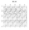
- FIGS. 4A and 4B are an equivalent circuit diagram showing a portion of a pixel array according to a second embodiment of the invention.
- FIG. 5 is a waveform diagram showing a data voltage applied to the pixel array shown in FIGS. 4A and 4B .
- the second embodiment of the invention arranges subpixels of the same color on four adjacent horizontal lines of the pixel array in a hexagonal shape as indicated by the dotted line.
- TFTs are disposed in a zigzag shape along the data lines, including e.g. data lines D1 to D10, so as to implement the DRD type pixel array.
- Two adjacent subpixels positioned on the left and right sides of one data line are sequentially charged to a data voltage from the one data line and share the one data line with each other.
- the output channels of the source driver ICs of the data driver 12 are respectively connected to the data lines, including e.g. data lines D1 to D10.
- the source driver ICs invert a horizontal polarity pattern in a cycle of two output channels. For example, during an Nth frame period, a horizontal polarity pattern of the data voltages output through (4i+1)th and (4i+2)th output channels of the source driver ICs is represented by "+ +", and a horizontal polarity pattern of the data voltages output through (4i+3)th and (4i+4)th output channels of the source driver ICs is represented by "- -”. Each of the source driver ICs may invert polarities of the output channels in each frame period.
- a horizontal polarity pattern of the data voltages output through the (4i+1)th and (4i+2)th output channels of the source driver ICs is represented by "- -”
- a horizontal polarity pattern of the data voltages output through the (4i+3)th and (4i+4)th output channels of the source driver ICs is represented by "+ +”.
- each source driver IC the data voltages of the same polarity, which will be charged to two adjacent subpixels positioned on the left and right sides of one data line, are successively output in one horizontal period 1H.
- the data voltages of the same polarity are supplied to the two adjacent subpixels through the one data line in one horizontal period 1H.
- each of the source driver ICs of the data driver 12 inverts the polarities of the data voltages in a horizontal 2-dot and vertical 2-dot inversion scheme.
- a polarity pattern of the pixel array follows a horizontal 4-dot and vertical 2-dot inversion scheme due to the structure of the DRD type pixel array.
- (4i+1)th and (4i+4)th horizontal lines of the pixel array (4i+1)th subpixels have the first color R; (4i+2)th subpixels have the second color G; (4i+3)th subpixels have the third color B; and (4i+4)th subpixels have the fourth color W.
- (4i+1)th subpixels have the third color B; (4i+2)th subpixels have the fourth color W; (4i+3)th subpixels have the first color R; and (4i+4)th subpixels have the second color G.
- +R (or +G, +B, and +W) data voltage is a positive R (or G, B, and W) data voltage
- -R (or -G, -B, and -W) data voltage is a negative R (or G, B, and W) data voltage
- T11 to T18 respectively denote eight TFTs disposed on the (4i+1)th and (4i+4)th horizontal lines of the pixel array from left to right in order.
- T21 to T28 respectively denote eight TFTs disposed on the (4i+2)th and (4i+3)th horizontal lines of the pixel array from left to right in order.
- the source driver ICs output the positive data voltage to the (4i+1)th and (4i+2)th data lines, including e.g. data lines D1, D2, D5, D6, D9, and D10, through the (4i+1)th and (4i+2)th output channels and output the negative data voltage to the (4i+3)th and (4i+4)th data lines, including e.g. data lines D3, D4, D7, and D8, through the (4i+3)th and (4i+4)th output channels.
- the data voltages output through all of the output channels of the source driver ICs are sequentially charged to the left subpixel and then the right subpixel on all of the horizontal lines of the pixel array as indicated by the arrows of FIGS. 4A and 4B .
- the gate driver 14 sequentially outputs the gate pulse synchronized with the data voltage.
- a first TFT T11 supplies the +R data voltage supplied through the first data line D1 to a first subpixel in response to a first gate pulse from a first gate line G1.
- a second TFT T12 supplies the +G data voltage supplied through the first data line D 1 to a second subpixel in response to a second gate pulse from a second gate line G2.
- the first subpixel is charged to the +R data voltage during the first half of a first horizontal period.
- the second subpixel is charged to the +G data voltage during the second half of the first horizontal period.
- a third TFT T13 supplies the +B data voltage supplied through the second data line D2 to a third subpixel in response to the first gate pulse.
- a fourth TFT T14 supplies the +W data voltage supplied through the second data line D2 to a fourth subpixel in response to the second gate pulse.
- the third subpixel is charged to the +B data voltage during the first half of the first horizontal period. Subsequently, the fourth subpixel is charged to the +W data voltage during the second half of the first horizontal period.
- a fifth TFT T15 supplies the -R data voltage supplied through the third data line D3 to a fifth subpixel in response to the first gate pulse.
- a sixth TFT T16 supplies the -G data voltage supplied through the third data line D3 to a sixth subpixel in response to the second gate pulse. The fifth subpixel is charged to the -R data voltage during the first half of the first horizontal period.
- the sixth subpixel is charged to the -G data voltage during the second half of the first horizontal period.
- a seventh TFT T17 supplies the -B data voltage supplied through the fourth data line D4 to a seventh subpixel in response to the first gate pulse.
- An eighth TFT T18 supplies the -W data voltage supplied through the fourth data line D4 to an eighth subpixel in response to the second gate pulse.
- the seventh subpixel is charged to the - B data voltage during the first half of the first horizontal period.
- the eighth subpixel is charged to the -W data voltage during the second half of the first horizontal period.
- a first TFT T21 supplies the -B data voltage supplied through the first data line D1 to a first subpixel in response to a third gate pulse from a third gate line G3.
- a second TFT T22 supplies the -W data voltage supplied through the first data line D1 to a second subpixel in response to a fourth gate pulse from a fourth gate line G4.
- the first subpixel is charged to the -B data voltage during the first half of a second horizontal period. Subsequently, the second subpixel is charged to the -W data voltage during the second half of the second horizontal period.
- a third TFT T23 supplies the -R data voltage supplied through the second data line D2 to a third subpixel in response to the third gate pulse.
- a fourth TFT T24 supplies the -G data voltage supplied through the second data line D2 to a fourth subpixel in response to the fourth gate pulse.
- the third subpixel is charged to the -R data voltage during the first half of the second horizontal period.
- the fourth subpixel is charged to the -G data voltage during the second half of the second horizontal period.
- a fifth TFT T25 supplies the +B data voltage supplied through the third data line D3 to a fifth subpixel in response to the third gate pulse.
- a sixth TFT T26 supplies the +W data voltage supplied through the third data line D3 to a sixth subpixel in response to the fourth gate pulse.
- the fifth subpixel is charged to the +B data voltage during the first half of the second horizontal period.
- a seventh TFT T27 supplies the +R data voltage supplied through the fourth data line D4 to a seventh subpixel in response to the third gate pulse.
- An eighth TFT T28 supplies the +G data voltage supplied through the fourth data line D4 to an eighth subpixel in response to the fourth gate pulse.
- the seventh subpixel is charged to the +R data voltage during the first half of the second horizontal period.
- the eighth subpixel is charged to the +G data voltage during the second half of the second horizontal period.
- a first TFT supplies the +B data voltage supplied through the first data line D1 to a first subpixel in response to a fifth gate pulse from a fifth gate line G5.
- a second TFT supplies the +W data voltage supplied through the first data line D1 to a second subpixel in response to a sixth gate pulse from a sixth gate line G6.
- the first subpixel is charged to the +B data voltage during the first half of a third horizontal period.
- the second subpixel is charged to the +W data voltage during the second half of the third horizontal period.
- a third TFT supplies the +R data voltage supplied through the second data line D2 to a third subpixel in response to the fifth gate pulse.
- a fourth TFT supplies the +G data voltage supplied through the second data line D2 to a fourth subpixel in response to the sixth gate pulse.
- the third subpixel is charged to the +R data voltage during the first half of the third horizontal period. Subsequently, the fourth subpixel is charged to the +G data voltage during the second half of the third horizontal period.
- a fifth TFT supplies the -B data voltage supplied through the third data line D3 to a fifth subpixel in response to the fifth gate pulse.
- a sixth TFT supplies the -W data voltage supplied through the third data line D3 to a sixth subpixel in response to the sixth gate pulse. The fifth subpixel is charged to the -B data voltage during the first half of the third horizontal period.
- the sixth subpixel is charged to the -W data voltage during the second half of the third horizontal period.
- a seventh TFT supplies the -R data voltage supplied through the fourth data line D4 to a seventh subpixel in response to the fifth gate pulse.
- An eighth TFT supplies the -G data voltage supplied through the fourth data line D4 to an eighth subpixel in response to the sixth gate pulse.
- the seventh subpixel is charged to the -R data voltage during the first half of the third horizontal period.
- the eighth subpixel is charged to the -G data voltage during the second half of the third horizontal period.
- a first TFT supplies the -R data voltage supplied through the first data line D1 to a first subpixel in response to a seventh gate pulse from a seventh gate line G7.
- a second TFT supplies the -G data voltage supplied through the first data line D1 to a second subpixel in response to an eighth gate pulse from an eighth gate line G8.
- the first subpixel is charged to the -R data voltage during the first half of a fourth horizontal period.
- the second subpixel is charged to the -G data voltage during the second half of the fourth horizontal period.
- a third TFT supplies the -B data voltage supplied through the second data line D2 to a third subpixel in response to the seventh gate pulse.
- a fourth TFT supplies the -W data voltage supplied through the second data line D2 to a fourth subpixel in response to the eighth gate pulse.
- the third subpixel is charged to the -B data voltage during the first half of the fourth horizontal period. Subsequently, the fourth subpixel is charged to the -W data voltage during the second half of the fourth horizontal period.
- a fifth TFT supplies the +R data voltage supplied through the third data line D3 to a fifth subpixel in response to the seventh gate pulse.
- a sixth TFT supplies the +G data voltage supplied through the third data line D3 to a sixth subpixel in response to the eighth gate pulse. The fifth subpixel is charged to the +R data voltage during the first half of the fourth horizontal period.
- the sixth subpixel is charged to the +G data voltage during the second half of the fourth horizontal period.
- a seventh TFT supplies the +B data voltage supplied through the fourth data line D4 to a seventh subpixel in response to the seventh gate pulse.
- An eighth TFT supplies the +W data voltage supplied through the fourth data line D4 to an eighth subpixel in response to the eighth gate pulse.
- the seventh subpixel is charged to the +B data voltage during the first half of the fourth horizontal period.
- the eighth subpixel is charged to the +W data voltage during the second half of the fourth horizontal period.
- the RGB subpixels of which the polarities are inverted in the dot inversion scheme, are arranged in the hexagonal shape (or honeycomb shape) based on the same color, and subpixels of the same color are uniformly distributed in strong charge subpixels and weak charge subpixels. Further, the W subpixels are configured as the strong charge subpixels. The polarities of the subpixels of each color are balanced. As a result, the display device according to the embodiment of the invention may implement the best image quality, in which there are no flicker, line noise, color distortion, etc.
- FIG. 6 is an equivalent circuit diagram showing a portion of a pixel array according to a third embodiment of the invention.
- subpixels of the same color are arranged on three adjacent horizontal lines of a pixel array in a diamond (or rhombus) shape.
- the W subpixels may increase the luminance of the input image and may reduce power consumption of the display device.
- One diamond has the size disposed on five vertical lines C1 to C5 and three horizontal lines L1 to L3.
- TFTs are disposed in a zigzag shape along the data lines, including e.g. data lines D1 to D6, so as to implement the DRD type pixel array.
- Two adjacent subpixels positioned on the left and right sides of one data line are sequentially charged to a data voltage from the one data line and share the one data line with each other.
- the output channels of the source driver ICs of the data driver 12 are respectively connected to the data lines, including e.g. data lines D1 to D6.
- Polarities of the data voltages output through odd-numbered output channels of the source driver ICs are opposite to polarities of the data voltages output through even-numbered output channels of the source driver ICs.
- a horizontal polarity pattern of the data voltages simultaneously output from the output channels of the source driver ICs has a repeat pattern of "+ - + -" during an Nth frame period and has a repeat pattern of "- + - +" during an (N+1)th frame period.
- each source driver IC the data voltages of the same polarity, which will be charged to two adjacent subpixels positioned on the left and right sides of one data line, are successively output in one horizontal period 1H.
- the data voltages of the same polarity are supplied to the two adjacent subpixels through the one data line in one horizontal period 1H.
- each of the source driver ICs of the data driver 12 inverts the polarities of the data voltages in a horizontal 1-dot and vertical 2-dot inversion scheme.
- a polarity pattern of the pixel array follows a horizontal 2-dot and vertical 2-dot inversion scheme due to the structure of the DRD type pixel array.
- (4i+1)th subpixels have the first color R; (4i+2)th subpixels have the second color G; (4i+3)th subpixels have the third color B; and (4i+4)th subpixels have the fourth color W.
- (4i+1)th subpixels have the third color B; (4i+2)th subpixels have the fourth color W; (4i+3)th subpixels have the first color R; and (4i+4)th subpixels have the second color G.
- +R (or +G, +B, and +W) data voltage is a positive R (or G, B, and W) data voltage
- -R (or -G, -B, and -W) data voltage is a negative R (or G, B, and W) data voltage
- T11 to T18 respectively denote eight TFTs disposed on the odd-numbered horizontal lines of the pixel array from left to right in order.
- T21 to T28 respectively denote eight TFTs disposed on the even-numbered horizontal lines of the pixel array from left to right in order.
- the source driver ICs output the positive data voltage to the odd-numbered data lines, including e.g. data lines D1, D3, and D5, through the odd-numbered output channels and output the negative data voltage to the even-numbered data lines, including e.g. data lines D2, D4, and D6, through the even-numbered output channels.
- the data voltages output through the odd-numbered output channels of the source driver ICs are sequentially charged to the left subpixel and then the right subpixel as indicated by the left arrow and right arrow of FIG. 6 .
- the data voltages output through the even-numbered output channels of the source driver ICs are sequentially charged to the right subpixel and then the left subpixel as indicated by the middle arrow of FIG. 6 .
- the gate driver 14 sequentially outputs the gate pulse synchronized with the data voltage.
- a first TFT T11 supplies the +R data voltage supplied through the first data line D1 to a first subpixel in response to a first gate pulse from a first gate line G1.
- a second TFT T12 supplies the +G data voltage supplied through the first data line D1 to a second subpixel in response to a second gate pulse from a second gate line G2.
- the first subpixel is charged to the +R data voltage during the first half of an odd-numbered horizontal period.
- the second subpixel is charged to the +G data voltage during the second half of the odd-numbered horizontal period.
- a third TFT T13 supplies the -B data voltage supplied through the second data line D2 to a third subpixel in response to the first gate pulse.
- a fourth TFT T14 supplies the -W data voltage supplied through the second data line D2 to a fourth subpixel in response to the second gate pulse.
- the third subpixel is charged to the -B data voltage during the first half of the odd-numbered horizontal period. Subsequently, the fourth subpixel is charged to the -W data voltage during the second half of the odd-numbered horizontal period.
- a fifth TFT T15 supplies the +R data voltage supplied through the third data line D3 to a fifth subpixel in response to the first gate pulse.
- a sixth TFT T16 supplies the +G data voltage supplied through the third data line D3 to a sixth subpixel in response to the second gate pulse. The fifth subpixel is charged to the +R data voltage during the first half of the odd-numbered horizontal period.
- the sixth subpixel is charged to the +G data voltage during the second half of the odd-numbered horizontal period.
- a seventh TFT T17 supplies the -B data voltage supplied through the fourth data line D4 to a seventh subpixel in response to the first gate pulse.
- An eighth TFT T18 supplies the -W data voltage supplied through the fourth data line D4 to an eighth subpixel in response to the second gate pulse.
- the seventh subpixel is charged to the - B data voltage during the first half of the odd-numbered horizontal period.
- the eighth subpixel is charged to the -W data voltage during the second half of the odd-numbered horizontal period.
- a first TFT T21 supplies the - B data voltage supplied through the first data line D1 to a first subpixel in response to a third gate pulse from a third gate line G3.
- a second TFT T22 supplies the -W data voltage supplied through the first data line D1 to a second subpixel in response to a fourth gate pulse from a fourth gate line G4.
- the first subpixel is charged to the -B data voltage during the first half of an even-numbered horizontal period.
- the second subpixel is charged to the -W data voltage during the second half of the even-numbered horizontal period.
- a third TFT T23 supplies the +R data voltage supplied through the second data line D2 to a third subpixel in response to the third gate pulse.
- a fourth TFT T24 supplies the +G data voltage supplied through the second data line D2 to a fourth subpixel in response to the fourth gate pulse.
- the fourth subpixel is charged to the +G data voltage during the first half of the even-numbered horizontal period.
- the third subpixel is charged to the +R data voltage during the second half of the even-numbered horizontal period.
- a fifth TFT T25 supplies the -B data voltage supplied through the third data line D3 to a fifth subpixel in response to the third gate pulse.
- a sixth TFT T26 supplies the -W data voltage supplied through the third data line D3 to a sixth subpixel in response to the fourth gate pulse.
- the fifth subpixel is charged to the -B data voltage during the first half of the even-numbered horizontal period.
- the sixth subpixel is charged to the -W data voltage during the second half of the even-numbered horizontal period.
- a seventh TFT T27 supplies the +R data voltage supplied through the fourth data line D4 to a seventh subpixel in response to the third gate pulse.
- An eighth TFT T28 supplies the +G data voltage supplied through the fourth data line D4 to an eighth subpixel in response to the fourth gate pulse.
- the eighth subpixel is charged to the +G data voltage during the first half of the even-numbered horizontal period.
- the seventh subpixel is charged to the +R data voltage during the second half of the even-numbered horizontal period.
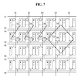
- FIG. 7 is an equivalent circuit diagram showing a portion of a pixel array according to a fourth embodiment of the invention.
- subpixels of the same color are arranged on three adjacent horizontal lines of a pixel array in a diamond shape.
- TFTs are disposed in a zigzag shape along the data lines, including e.g. data lines D1 to D6, so as to implement the DRD type pixel array.
- Two adjacent subpixels positioned on the left and right sides of one data line are sequentially charged to a data voltage from the one data line and share the one data line with each other.
- the output channels of the source driver ICs of the data driver 12 are respectively connected to the data lines, including e.g. data lines D1 to D6.
- Polarities of the data voltages output through odd-numbered output channels of the source driver ICs are opposite to polarities of the data voltages output through even-numbered output channels of the source driver ICs.
- a horizontal polarity pattern of the data voltages simultaneously output from the output channels of the source driver ICs has a repeat pattern of "+ - + -" during an Nth frame period and has a repeat pattern of "- + - +" during an (N+1)th frame period.
- each source driver IC the data voltages of the same polarity, which will be charged to two adjacent subpixels positioned on the left and right sides of one data line, are successively output in one horizontal period 1H.
- the data voltages of the same polarity are supplied to the two adjacent subpixels through the one data line in one horizontal period 1H.
- each of the source driver ICs of the data driver 12 inverts the polarities of the data voltages in a horizontal 1-dot and vertical 2-dot inversion scheme.
- a polarity pattern of the pixel array follows a horizontal 2-dot and vertical 2-dot inversion scheme due to the structure of the DRD type pixel array.
- (4i+1)th subpixels have the first color R; (4i+2)th subpixels have the second color G; (4i+3)th subpixels have the third color B; and (4i+4)th subpixels have the fourth color W.
- (4i+1)th subpixels have the third color B; (4i+2)th subpixels have the fourth color W; (4i+3)th subpixels have the first color R; and (4i+4)th subpixels have the second color G.
- +R (or +G, +B, and +W) data voltage is a positive R (or G, B, and W) data voltage
- -R (or -G, -B, and -W) data voltage is a negative R (or G, B, and W) data voltage
- T11 to T14 respectively denote four TFTs disposed on the odd-numbered horizontal lines of the pixel array from left to right in order.
- T21 to T24 respectively denote four TFTs disposed on the even-numbered horizontal lines of the pixel array from left to right in order.
- the source driver ICs output the positive data voltage to the odd-numbered data lines, including e.g. data lines D1, D3, and D5, through the odd-numbered output channels and output the negative data voltage to the even-numbered data lines, including e.g. data lines D2, D4, and D6, through the even-numbered output channels.
- the data voltages are sequentially charged to the left subpixel and then the right subpixel on each horizontal line of the pixel array as indicated by the arrows of FIG. 7 .
- a first TFT T11 supplies the +R data voltage supplied through the first data line D1 to a first subpixel in response to a first gate pulse from a first gate line G1.
- a second TFT T12 supplies the +G data voltage supplied through the first data line D1 to a second subpixel in response to a second gate pulse from a second gate line G2.
- the first subpixel is charged to the +R data voltage during the first half of an odd-numbered horizontal period.
- the second subpixel is charged to the +G data voltage during the second half of the odd-numbered horizontal period.
- a third TFT T13 supplies the -B data voltage supplied through the second data line D2 to a third subpixel in response to the first gate pulse.
- a fourth TFT T14 supplies the -W data voltage supplied through the second data line D2 to a fourth subpixel in response to the second gate pulse.
- the third subpixel is charged to the -B data voltage during the first half of the odd-numbered horizontal period. Subsequently, the fourth subpixel is charged to the -W data voltage during the second half of the odd-numbered horizontal period.
- a first TFT T21 supplies the - B data voltage supplied through the first data line D1 to a first subpixel in response to a third gate pulse from a third gate line G3.
- a second TFT T22 supplies the -W data voltage supplied through the first data line D1 to a second subpixel in response to a fourth gate pulse from a fourth gate line G4.
- the first subpixel is charged to the -B data voltage during the first half of an even-numbered horizontal period.
- the second subpixel is charged to the -W data voltage during the second half of the even-numbered horizontal period.
- a third TFT T23 supplies the +R data voltage supplied through the second data line D2 to a third subpixel in response to the third gate pulse.
- a fourth TFT T24 supplies the +G data voltage supplied through the second data line D2 to a fourth subpixel in response to the fourth gate pulse.
- the third subpixel is charged to the +R data voltage during the first half of the even-numbered horizontal period.
- the fourth subpixel is charged to the +G data voltage during the second half of the even-numbered horizontal period.
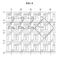
- FIG. 8 is an equivalent circuit diagram showing a portion of a pixel array according to a fifth embodiment of the invention.
- subpixels of the same color are arranged on three adjacent horizontal lines of a pixel array in a diamond shape.
- TFTs are disposed in a zigzag shape along the data lines, including e.g. data lines D1 to D6, so as to implement the DRD type pixel array.
- Two adjacent subpixels positioned on the left and right sides of one data line are sequentially charged to a data voltage from the one data line and share the one data line with each other.
- the output channels of the source driver ICs of the data driver 12 are respectively connected to the data lines, including e.g. data lines D1 to D6.
- Polarities of the data voltages output through (4i+1)th and (4i+2)th output channels of the source driver ICs are opposite to polarities of the data voltages output through (4i+3)th and (4i+4)th output channels of the source driver ICs.
- a horizontal polarity pattern of the data voltages simultaneously output from the output channels of the source driver ICs has a repeat pattern of "+ + - -" during an Nth frame period and has a repeat pattern of "- - + +" during an (N+1)th frame period.
- each source driver IC the data voltages of the same polarity, which will be charged to two adjacent subpixels positioned on the left and right sides of one data line, are successively output in one horizontal period 1H.
- the data voltages of the same polarity are supplied to the two adjacent subpixels through the one data line in one horizontal period 1H.
- each of the source driver ICs of the data driver 12 inverts the polarities of the data voltages in a horizontal 2-dot and vertical 2-dot inversion scheme.
- a polarity pattern of the pixel array follows a horizontal 4-dot and vertical 2-dot inversion scheme due to the structure of the DRD type pixel array.
- (4i+1)th subpixels have the first color R; (4i+2)th subpixels have the second color G; (4i+3)th subpixels have the third color B; and (4i+4)th subpixels have the fourth color W.
- (4i+1)th subpixels have the third color B; (4i+2)th subpixels have the fourth color W; (4i+3)th subpixels have the first color R; and (4i+4)th subpixels have the second color G.
- +R (or +G, +B, and +W) data voltage is a positive R (or G, B, and W) data voltage
- -R (or -G, -B, and -W) data voltage is a negative R (or G, B, and W) data voltage
- T11 to T18 respectively denote eight TFTs disposed on the odd-numbered horizontal lines of the pixel array from left to right in order.
- T21 to T28 respectively denote eight TFTs disposed on the even-numbered horizontal lines of the pixel array from left to right in order.
- the source driver ICs output the positive data voltage to the (4i+1)th and (4i+2)th data lines, including e.g. data lines D1, D2, D5, and D6, through the (4i+1)th and (4i+2)th output channels and output the negative data voltage to the (4i+3)th and (4i+4)th data lines, including e.g. data lines D3 and D4, through the (4i+3)th and (4i+4)th output channels.
- the data voltages are sequentially charged to the left subpixel and then the right subpixel on each horizontal line of the pixel array as indicated by the arrows of FIG. 8 .
- a first TFT T11 supplies the +R data voltage supplied through the first data line D1 to a first subpixel in response to a first gate pulse from a first gate line G1.
- a second TFT T12 supplies the +G data voltage supplied through the first data line D1 to a second subpixel in response to a second gate pulse from a second gate line G2.
- the first subpixel is charged to the +R data voltage during the first half of an odd-numbered horizontal period.
- the second subpixel is charged to the +G data voltage during the second half of the odd-numbered horizontal period.
- a third TFT T13 supplies the +B data voltage supplied through the second data line D2 to a third subpixel in response to the first gate pulse.
- a fourth TFT T14 supplies the +W data voltage supplied through the second data line D2 to a fourth subpixel in response to the second gate pulse.
- the third subpixel is charged to the +B data voltage during the first half of the odd-numbered horizontal period.
- the fourth subpixel is charged to the +W data voltage during the second half of the odd-numbered horizontal period.
- a fifth TFT T15 supplies the -R data voltage supplied through the third data line D3 to a fifth subpixel in response to the first gate pulse.
- a sixth TFT T16 supplies the -G data voltage supplied through the third data line D3 to a sixth subpixel in response to the second gate pulse.
- the fifth subpixel is charged to the - R data voltage during the first half of the odd-numbered horizontal period.
- the sixth subpixel is charged to the -G data voltage during the second half of the odd-numbered horizontal period.
- a seventh TFT T17 supplies the -B data voltage supplied through the fourth data line D4 to a seventh subpixel in response to the first gate pulse.
- An eighth TFT T18 supplies the -W data voltage supplied through the fourth data line D4 to an eighth subpixel in response to the second gate pulse.
- the seventh subpixel is charged to the -B data voltage during the first half of the odd-numbered horizontal period.
- the eighth subpixel is charged to the -W data voltage during the second half of the odd-numbered horizontal period.
- a first TFT T21 supplies the - B data voltage supplied through the first data line D1 to a first subpixel in response to a third gate pulse from a third gate line G3.
- a second TFT T22 supplies the -W data voltage supplied through the first data line D1 to a second subpixel in response to a fourth gate pulse from a fourth gate line G4.
- the first subpixel is charged to the -B data voltage during the first half of an even-numbered horizontal period.
- the second subpixel is charged to the -W data voltage during the second half of the even-numbered horizontal period.
- a third TFT T23 supplies the -R data voltage supplied through the second data line D2 to a third subpixel in response to the third gate pulse.
- a fourth TFT T24 supplies the -G data voltage supplied through the second data line D2 to a fourth subpixel in response to the fourth gate pulse.
- the third subpixel is charged to the -R data voltage during the first half of the even-numbered horizontal period.
- the fourth subpixel is charged to the -G data voltage during the second half of the even-numbered horizontal period.
- a fifth TFT T25 supplies the +B data voltage supplied through the third data line D3 to a fifth subpixel in response to the third gate pulse.
- a sixth TFT T26 supplies the +W data voltage supplied through the third data line D3 to a sixth subpixel in response to the fourth gate pulse.
- the fifth subpixel is charged to the +B data voltage during the first half of the even-numbered horizontal period.
- a seventh TFT T27 supplies the +R data voltage supplied through the fourth data line D4 to a seventh subpixel in response to the third gate pulse.
- An eighth TFT T28 supplies the +G data voltage supplied through the fourth data line D4 to an eighth subpixel in response to the fourth gate pulse.
- the seventh subpixel is charged to the +R data voltage during the first half of the even-numbered horizontal period.
- the eighth subpixel is charged to the +G data voltage during the second half of the even-numbered horizontal period.
- FIG. 9 is an equivalent circuit diagram showing a portion of a pixel array according to a sixth embodiment of the invention.
- subpixels of the same color are arranged on three adjacent horizontal lines of a pixel array in a diamond shape.
- TFTs are disposed in a zigzag shape along the data lines, including e.g. D1 to D6, so as to implement the DRD type pixel array.
- Two adjacent subpixels positioned on the left and right sides of one data line are sequentially charged to a data voltage from the one data line and share the one data line with each other.
- the output channels of the source driver ICs of the data driver 12 are respectively connected to the data lines, including e.g. data lines D1 to D6.
- the source driver ICs invert a horizontal polarity pattern in a cycle of four output channels. For example, during an Nth frame period, a horizontal polarity pattern of the data voltages output through (8i+1)th to (8i+4)th output channels of the source driver ICs is represented by "+ - + -", and a horizontal polarity pattern of the data voltages output through (8i+5)th to (8i+8)th output channels of the source driver ICs is represented by "- + - +".
- a horizontal polarity pattern of the data voltages output through the (8i+1)th to (8i+4)th output channels of the source driver ICs is represented by "- + - +"
- a horizontal polarity pattern of the data voltages output through the (8i+5)th to (8i+8)th output channels of the source driver ICs is represented by "+ - + -”.
- a polarity pattern of a second pixel group H4CH2 is an inverse polarity pattern of a polarity pattern of a first pixel group H4CH1.
- the TFTs of the first pixel group H4CH1 and the TFTs of the second pixel group H4CH2 are disposed in a left-right symmetrical manner based on a boundary between the first and second pixel groups H4CH1 and H4CH2.
- each source driver IC the data voltages of the same polarity, which will be charged to two adjacent subpixels positioned on the left and right sides of one data line, are successively output in one horizontal period 1H.
- the data voltages of the same polarity are supplied to the two adjacent subpixels through the one data line in one horizontal period 1H.
- each of the source driver ICs of the data driver 12 inverts the polarities of the data voltages in a horizontal 1-dot and vertical 2-dot inversion scheme.
- a polarity pattern of the pixel array follows a horizontal 2-dot and vertical 2-dot inversion scheme due to the structure of the DRD type pixel array.
- (4i+1)th subpixels have the first color R; (4i+2)th subpixels have the second color G; (4i+3)th subpixels have the third color B; and (4i+4)th subpixels have the fourth color W.
- (4i+1)th subpixels have the third color B; (4i+2)th subpixels have the fourth color W; (4i+3)th subpixels have the first color R; and (4i+4)th subpixels have the second color G.
- +R (or +G, +B, and +W) data voltage is a positive R (or G, B, and W) data voltage
- -R (or -G, -B, and -W) data voltage is a negative R (or G, B, and W) data voltage
- T11 to T18 respectively denote eight TFTs disposed on the odd-numbered horizontal lines of the pixel array from left to right in order.
- T21 to T28 respectively denote eight TFTs disposed on the even-numbered horizontal lines of the pixel array from left to right in order.
- the source driver ICs output the positive data voltage to the odd-numbered data lines, including e.g. data lines D1, D3, and D5, through the odd-numbered output channels and output the negative data voltage to the even-numbered data lines, including e.g. data lines D2, D4, and D6, through the even-numbered output channels.
- the data voltages output through the (8i+1)th, (8i+4)th, (8i+6)th, and (8i+7)th output channels of the source driver ICs are sequentially charged to the left subpixel and then the right subpixel as indicated by the left arrow of FIG. 9 .
- the data voltages output through the (8i+2)th, (8i+3)th, (8i+5)th, and (8i+8)th output channels of the source driver ICs are sequentially charged to the right subpixel and then the left subpixel as indicated by the middle arrow and right arrow of FIG. 9 .
- the gate driver 14 sequentially outputs the gate pulse synchronized with the data voltage.
- a first TFT T11 supplies the +R data voltage supplied through the first data line D1 to a first subpixel in response to a first gate pulse from a first gate line G1.
- a second TFT T12 supplies the +G data voltage supplied through the first data line D1 to a second subpixel in response to a second gate pulse from a second gate line G2.
- the first subpixel is charged to the +R data voltage during the first half of an odd-numbered horizontal period.
- the second subpixel is charged to the +G data voltage during the second half of the odd-numbered horizontal period.
- a third TFT T13 supplies the -B data voltage supplied through the second data line D2 to a third subpixel in response to the second gate pulse.
- a fourth TFT T14 supplies the -W data voltage supplied through the second data line D2 to a fourth subpixel in response to the first gate pulse.
- the fourth subpixel is charged to the -W data voltage during the first half of the odd-numbered horizontal period.
- the third subpixel is charged to the -B data voltage during the second half of the odd-numbered horizontal period.
- a fifth TFT T15 supplies the +R data voltage supplied through the third data line D3 to a fifth subpixel in response to the second gate pulse.
- a sixth TFT T16 supplies the +G data voltage supplied through the third data line D3 to a sixth subpixel in response to the first gate pulse.
- the sixth subpixel is charged to the +G data voltage during the first half of the odd-numbered horizontal period.
- the fifth subpixel is charged to the +R data voltage during the second half of the odd-numbered horizontal period.
- a seventh TFT T17 supplies the -B data voltage supplied through the fourth data line D4 to a seventh subpixel in response to the first gate pulse.
- An eighth TFT T18 supplies the -W data voltage supplied through the fourth data line D4 to an eighth subpixel in response to the second gate pulse.
- the seventh subpixel is charged to the -B data voltage during the first half of the odd-numbered horizontal period.
- the eighth subpixel is charged to the -W data voltage during the second half of the odd-numbered horizontal period.
- a first TFT T21 supplies the - B data voltage supplied through the first data line D1 to a first subpixel in response to a third gate pulse from a third gate line G3.
- a second TFT T22 supplies the -W data voltage supplied through the first data line D1 to a second subpixel in response to a fourth gate pulse from a fourth gate line G4.
- the first subpixel is charged to the -B data voltage during the first half of an even-numbered horizontal period. Subsequently, the second subpixel is charged to the -W data voltage during the second half of the even-numbered horizontal period.
- a third TFT T23 supplies the +R data voltage supplied through the second data line D2 to a third subpixel in response to the fourth gate pulse.
- a fourth TFT T24 supplies the +G data voltage supplied through the second data line D2 to a fourth subpixel in response to the third gate pulse.
- the fourth subpixel is charged to the +G data voltage during the first half of the even-numbered horizontal period.
- the third subpixel is charged to the +R data voltage during the second half of the even-numbered horizontal period.
- a fifth TFT T25 supplies the -B data voltage supplied through the third data line D3 to a fifth subpixel in response to the fourth gate pulse.
- a sixth TFT T26 supplies the -W data voltage supplied through the third data line D3 to a sixth subpixel in response to the third gate pulse. The sixth subpixel is charged to the -W data voltage during the first half of the even-numbered horizontal period.
- the fifth subpixel is charged to the -B data voltage during the second half of the even-numbered horizontal period.
- a seventh TFT T27 supplies the +R data voltage supplied through the fourth data line D4 to a seventh subpixel in response to the third gate pulse.
- An eighth TFT T28 supplies the +G data voltage supplied through the fourth data line D4 to an eighth subpixel in response to the fourth gate pulse.
- the seventh subpixel is charged to the +R data voltage during the first half of the even-numbered horizontal period.
- the eighth subpixel is charged to the +G data voltage during the second half of the even-numbered horizontal period.
- each pixel is divided into subpixels of four colors.
- each of odd-numbered pixels may include RGBW subpixels disposed in a triangular or rectangular shape on adjacent odd-numbered horizontal lines LINE#1 and LINE#3 and even-numbered horizontal lines LINE#2 and LINE#4, so as to dispose the pixels without a reduction in a horizontal resolution.
- the RGBW subpixels may include color filters CF formed on an upper substrate SUBS 1.
- the RGB color filters may be formed of an acrylic resin, to which a pigment is added.
- the W color filter may be formed of an acrylic resin not containing a pigment and may be thicker than other color filters. In this instance, there is a difference between a cell gap CG1 of the RGB subpixels and a cell gap CG2 of the W subpixel.
- a phase retardation of liquid crystals between the RGB subpixels and the W subpixel may vary due to the difference between the cell gaps CG1 and CG2.
- light intensity of the W subpixel may vary, compared to the RGB subpixels.
- Various embodiments of the invention may prevent the W subpixels from being displayed more conspicuously than the RGB subpixels by arranging the W subpixels in not a line shape but the hexagonal shape or the diamond shape.
- BM denotes a black matrix
- CS denotes a column spacer
- PAC denotes an organic protective layer (e.g., made of photo-acryl) covering a TFT array formed on a lower substrate SUBS2.
- various embodiments of the invention arrange the RGBW subpixels in the hexagonal shape or the diamond shape based on the same color.
- the embodiments of the invention may achieve the excellent display quality of the image without a reduction in the image quality, such as the line noise and the color distortion, in the RGBW type display device.
Landscapes
- Engineering & Computer Science (AREA)
- Physics & Mathematics (AREA)
- Computer Hardware Design (AREA)
- General Physics & Mathematics (AREA)
- Theoretical Computer Science (AREA)
- Chemical & Material Sciences (AREA)
- Crystallography & Structural Chemistry (AREA)
- Control Of Indicators Other Than Cathode Ray Tubes (AREA)
- Liquid Crystal Display Device Control (AREA)
- Liquid Crystal (AREA)
- Devices For Indicating Variable Information By Combining Individual Elements (AREA)
Abstract
Description
- Embodiments of the invention relate to a display device, in which each pixel is divided into four color subpixels.
- Various flat panel displays, such as a liquid crystal display (LCD), a plasma display panel (PDP), an organic light emitting display, and an electrophoresis display (EPD), have been developed. The liquid crystal display displays an image by controlling an electric field applied to liquid crystal molecules based on a data voltage. An active matrix liquid crystal display includes a thin film transistor (TFT) in each pixel. The pixels of the liquid crystal display may be divided into red (R) subpixels, green (G) subpixels, blue (B) subpixels, and white (W) subpixels, so as to represent colors and increase a luminance. In the following description, the display device, in which the pixels are divided into the RGBW subpixels, is referred to as an RGBW type display device.
- The liquid crystal display includes a liquid crystal display panel, a backlight unit providing light to the liquid crystal display panel, source driver integrated circuits (ICs) for supplying a data voltage to data lines of the liquid crystal display panel, gate driver ICs for supplying a gate pulse (or scan pulse) to gate lines (or scan lines) of the liquid crystal display panel, a control circuit for controlling the source driver ICs and the gate driver ICs, a light source driving circuit for driving light sources of the backlight unit, etc.
- In an inversion scheme of the liquid crystal display, polarities of the data voltages charged to adjacent subpixels are opposite to each other and are periodically inverted, so as to reduce DC image sticking and prevent the degradation of liquid crystals. A horizontal and vertical 1-dot inversion scheme or a horizontal 1-dot and vertical 2-dot inversion scheme has been applied to most of the liquid crystal displays. The 1-dot means one subpixel.
- A charge amount of subpixels of each color may vary depending on a relationship between data of an input image and a polarity pattern of the pixels. In this instance, a line noise of a longitudinal line shape and color distortion may appear in an image displayed on a pixel array due to the color arrangement of the subpixels.
- Embodiments of the invention provide a liquid crystal display, in which each pixels is divided into four color subpixels, capable of improving the display quality.
- In one aspect, there is a display panel (10) comprising a plurality of data lines (D1 to Dm) and a plurality of gate lines (G1 to Gn) intersecting the data lines (D1 to Dm); a pixel array comprising a plurality of pixels arranged in a matrix form and coupled to the data lines (D1 to Dm) and gate lines (G1 to Gn), each pixel being divided into a first subpixel having a first color (R), a second subpixel having a second color (G), a third subpixel having a third color (B), and a fourth subpixel having a fourth color (W), wherein two adjacent subpixels in a horizontal line of the pixel array share a data line of the plurality of data lines (D1 to Dm); wherein the subpixels of the plurality of pixels of the pixel array are arranged such that subpixels having the same color and arranged in four adjacent horizontal lines of the pixel array form a hexagonal shape.
- In one aspect, there is a display device comprising the display panel; a display panel driving circuit comprising a timing controller, a data driver (12) coupled to the data lines (D1 to Dm) and configured to provide data voltages to the data lines, and a gate driver (14) coupled to the gate lines (G1 to Gn) and configured to provide scan pulses to the gate lines.
- The accompanying drawings, which are included to provide a further understanding of the invention and are incorporated in and constitute a part of this specification, illustrate embodiments of the invention and together with the description serve to explain the principles of the invention. In the drawings:
-
FIG. 1 is a block diagram of a liquid crystal display according to an exemplary embodiment of the invention; -
FIGS. 2A and2B are an equivalent circuit diagram showing a portion of a pixel array according to a first embodiment of the invention; -
FIG. 3 is a waveform diagram showing a data voltage applied to the pixel array shown inFIGS. 2A and2B ; -
FIGS. 4A and4B are an equivalent circuit diagram showing a portion of a pixel array according to a second embodiment of the invention; -
FIG. 5 is a waveform diagram showing a data voltage applied to the pixel array shown inFIGS. 4A and4B ; -
FIG. 6 is an equivalent circuit diagram showing a portion of a pixel array according to a third embodiment of the invention; -
FIG. 7 is an equivalent circuit diagram showing a portion of a pixel array according to a fourth embodiment of the invention; -
FIG. 8 is an equivalent circuit diagram showing a portion of a pixel array according to a fifth embodiment of the invention; -
FIG. 9 is an equivalent circuit diagram showing a portion of a pixel array according to a sixth embodiment of the invention; -
FIGS. 10 and 11 illustrate an arrangement of subpixels in each pixel according to an exemplary embodiment of the invention; and -
FIG. 12 illustrates a color filter of a display device according to an exemplary embodiment of the invention. - Reference will now be made in detail to embodiments of the invention, examples of which are illustrated in the accompanying drawings. Wherever possible, the same reference numbers will be used throughout the drawings to refer to the same or like parts. It will be paid attention that detailed description of known arts will be omitted if it is determined that the arts can mislead the embodiments of the invention.
- A display device according to an exemplary embodiment of the invention may be implemented as a flat panel display capable of representing colors, such as a liquid crystal display (LCD), a plasma display panel (PDP), and an organic light emitting display. In the following description, the embodiments of the invention will be described using the liquid crystal display as an example of the flat panel display. Other flat panel displays may be used. For example, an arrangement of red (R), green (G), blue (B), and white (W) subpixels according to the embodiments of the invention may be applied to the organic light emitting display.
- As shown in
FIG. 1 , a display device according to an exemplary embodiment of the invention includes adisplay panel 10 including a pixel array and a display panel driving circuit for writing data of an input image on thedisplay panel 10. A backlight unit uniformly providing light to thedisplay panel 10 may be disposed under thedisplay panel 10. - The
display panel 10 includes an upper substrate and a lower substrate, which are positioned opposite each other with a liquid crystal layer interposed therebetween. The pixel array of thedisplay panel 10 includes pixels arranged in a matrix form based on a crossing structure of data lines D1 to Dm and gate lines G1 to Gn. - The pixel array including the data lines D1 to Dm, the gate lines G1 to Gn, thin film transistors (TFTs),
pixel electrodes 1 connected to the TFTs, storage capacitors Cst connected to thepixel electrodes 1, etc. is formed on the lower substrate of thedisplay panel 10. Each pixel adjusts a transmission amount of light using liquid crystal molecules driven by a voltage difference between thepixel electrode 1 charged to a data voltage through the TFT and acommon electrode 2, to which a common voltage Vcom is supplied, thereby displaying an image of video data. Each pixel is divided into red (R), green (G), blue (B), and white (W) subpixels. The RGBW subpixels may be arranged based on configurations shown inFIGS. 2A to 11 . - A color filter array including black matrixes and color filters is formed on the upper substrate of the
display panel 10. In a vertical electric field driving manner such as a twisted nematic (TN) mode and a vertical alignment (VA) mode, thecommon electrodes 2 are formed on the upper substrate. In a horizontal electric field driving manner such as an in-plane switching (IPS) mode and a fringe field switching (FFS) mode, thecommon electrodes 2 are formed on the lower substrate along with thepixel electrodes 1. Polarizing plates are respectively attached to the upper substrate and the lower substrate of thedisplay panel 10. Alignment layers for setting a pre-tilt angle of liquid crystals are respectively formed on the upper and lower substrates (e.g., glass substrates) of thedisplay panel 10. - The liquid crystal display according to the embodiment of the invention may be implemented as any type of liquid crystal display including a transmissive liquid crystal display, a transflective liquid crystal display, and a reflective liquid crystal display. The transmissive liquid crystal display and the transflective liquid crystal display require the backlight unit. The backlight unit may be implemented as a direct type backlight unit or an edge type backlight unit.
- The display panel driving circuit writes data on the pixels. The display panel driving circuit includes a
data driver 12, agate driver 14, and atiming controller 20. - The
data driver 12 includes a plurality of source driver integrated circuits (ICs). Output channels of the source driver ICs are connected to the data lines D1 to Dm of the pixel array. The total number of output channels of the source driver ICs is reduced to about 1/2 of the total number of data lines D1 to Dm due to a structure of the pixel array shown inFIGS. 2A to 11 . Thus, the manufacturing cost of the display device according to the embodiment of the invention may be reduced. - The
data driver 12 receives data of the input image from thetiming controller 20. Digital video data transmitted to thedata driver 12 includes red (R) data, green (G) data, blue (B) data, and white (W) data. Thedata driver 12 converts the RGBW digital video data of the input image into positive and negative gamma compensation voltages under the control of thetiming controller 20 and outputs positive and negative data voltages. An output voltage of thedata driver 12 is supplied to the data lines D1 to Dm. - The
gate driver 14 sequentially supplies a gate pulse to the gate lines G1 to Gn under the control of thetiming controller 20. The gate pulse output from thegate driver 14 is synchronized with positive and negative video data voltages, which will be charged to the pixels. - The
timing controller 20 converts the RGB data of the input image received from ahost system 30 into RGBW data and transmits the RGBW data to thedata driver 12. An interface for data transmission between the timingcontroller 20 and the source driver ICs of thedata driver 12 may use a mini low voltage differential signaling (LVDS) interface or an embedded panel interface (EPI). The EPI may use interface technologies disclosed in Korean Patent Application No.10-2008-0127458 (December 15, 2008 U.S. Patent Application No. 12/543,996 (August 19, 2009 10-2008-0127456 (December 15, 2008 U.S. Patent Application No. 12/461,652 (August 19, 2009 10-2008-0132466 (December 23, 2008 U.S. Patent Application No. 12/537,341 (August 7, 2009 - The
timing controller 20 receives timing signals synchronized with the data of the input image from thehost system 30. The timing signals include a vertical sync signal Vsync, a horizontal sync signal Hsync, a data enable signal DE, and a dot clock DCLK, etc. Thetiming controller 20 controls operation timings of thedata driver 12 and thegate driver 14 based on the timing signals Vsync, Hsync, DE, and DCLK received along with pixel data of the input image. Thetiming controller 20 may transmit polarity information of data for controlling polarities of the pixel array to each of the source driver ICs of thedata driver 12. The mini LVDS interface is an interface technology for transmitting a polarity control signal through a separate control line. The EPI is an interface technology which encodes polarity control information to a control data packet transmitted between a clock training pattern for clock and data recovery (CDR) and an RGBW data packet and transmits the polarity control information to each of the source driver ICs of thedata driver 12. - The
timing controller 20 may convert the RGB data of the input image into the RGBW data using a white gain calculation algorithm. Any known white gain calculation algorithm may be used. For example, the embodiment of the invention may use white gain calculation algorithms disclosed in Korean Patent Application Nos.10-2005-0039728 (May 12, 2005 10-2005-0052906(June 20, 2005 10-2005-0066429(July 21, 2007 10-2006-0011292 (February 6, 2006 - The
host system 30 may be implemented as one of a television system, a set-top box, a navigation system, a DVD player, a Blu-ray player, a personal computer (PC), a home theater system, and a phone system. - Various embodiments of the invention configure the structure of the pixel array into a double rate driving (DRD) type pixel array, in which two horizontally adjacent subpixels (e.g., two subpixels that are adjacent in a direction parallel to the gate lines) share one data line with each other as shown in
FIGS. 2A to 9 , so as to reduce the number of source driver ICs of thedata driver 12. The source driver ICs used in the DRD type pixel array increase a frequency of the data voltage to double. The DRD type pixel array may reduce the number of source driver ICs to one half. - Various embodiments of the invention propose that the pixels of the pixel array are arranged based on the configurations shown in
FIGS. 2A to 11 , so as to uniformize data charge characteristics of the RGBW subpixels based on the colors of the subpixels and prevent the color distortion. Various embodiments of the invention also propose that a polarity pattern of the pixel array is implemented as shown inFIGS. 2A to 11 , so as to uniformize polarities of the pixel array based on the colors of the subpixels. In the following embodiments, red, green, blue, and white are referred to as a first color R, a second color G, a third color B, and a fourth color W, as an example. However, the embodiments of the invention are not limited thereto. - Various embodiments of the invention control the polarity pattern of the pixel array in a dot inversion scheme inverting a polarity between the adjacent subpixels along vertical and horizontal directions. The vertical direction may be a direction parallel to the data lines, and the horizontal direction may be a direction parallel to the gate lines. The polarity pattern of the pixel array is determined depending on a polarity of the data voltage output from each of the source driver ICs of the
data driver 12 and the structure of the pixel array. - A horizontal polarity pattern of the pixel array is determined depending on the polarities of the data voltages which are simultaneously output through the output channels of the source driver ICs. For example, when "+" and "-" respectively indicate a positive polarity and a negative polarity, the horizontal polarity pattern, in which the polarities of the data voltages simultaneously output through the output channels of the source driver ICs are represented by "+ - + -" or "- + - +" from left to right, is referred to as a horizontal 1-dot inversion scheme. Further, the horizontal polarity pattern, in which the polarities of the data voltages are represented by "+ + - -" or "- - + +" from left to right, is referred to as a horizontal 2-dot inversion scheme.
- A vertical polarity pattern of the pixel array is determined depending on changes in the polarities of the data voltages, which are output through the output channels of the source driver ICs, as time passed. For example, the vertical polarity pattern, in which the polarities of the data voltages output through the output channels of the source driver ICs are represented by "+ - + -" or "- + - +" as time passed, is referred to as a vertical 1-dot inversion scheme. Further, the vertical polarity pattern, in which the polarities of the data voltages output through the output channels of the source driver ICs are represented by "+ + - -" or "- - + +" as time passed, is referred to as a vertical 2-dot inversion scheme.
-
FIGS. 2A and2B are an equivalent circuit diagram showing a portion of a pixel array according to a first embodiment of the invention.FIG. 3 is a waveform diagram showing a data voltage applied to the pixel array shown inFIGS. 2A and2B . - As shown in
FIGS. 2A to 3 , R subpixels, G subpixels, B subpixels, and W subpixels on first to fourth lines of a pixel array are individually arranged in a hexagonal shape (or a honeycomb shape) as indicated by the dotted line. The W subpixels may increase a luminance of the input image and may reduce power consumption of the display device. Namely, the embodiment of the invention arranges subpixels of the same color on four adjacent horizontal lines of the pixel array in the hexagonal shape as indicated by the dotted line. One hexagon has the size disposed on five vertical lines C1 to C5 and four horizontal lines L1 to L4. - The embodiment of the invention arranges the TFTs for connecting the
pixel electrode 1 of the subpixels to the data lines in a zigzag shape along the data lines, so as to implement the DRD type pixel array. The two adjacent subpixels positioned on the left and right sides of one data line are sequentially charged to the data voltage from the one data line and share the one data line with each other. The output channels of the source driver ICs are respectively connected to the data lines, including e.g. data lines D1 to D10. - The source driver ICs invert a horizontal polarity pattern in a cycle of four output channels. For example, during an Nth frame period (where N is a positive integer), a horizontal polarity pattern of the data voltages output through (8i+1)th to (8i+4)th output channels of the source driver ICs is represented by "+ - + -", and a horizontal polarity pattern of the data voltages output through (8i+5)th to (8i+8)th output channels of the source driver ICs is represented by "- + - +", where 'i' is zero and a positive integer, i.e. i = 0, 1, 2, 3, 4, ..., etc. Each of the source driver ICs may invert polarities of the output channels in each frame period. In this instance, during an (N+1)th frame period, a horizontal polarity pattern of the data voltages output through the (8i+1)th to (8i+4)th output channels of the source driver ICs is represented by "- + - +", and a horizontal polarity pattern of the data voltages output through the (8i+5)th to (8i+8)th output channels of the source driver ICs is represented by "+ - + -". In
FIGS. 2A and2B , 'H4CH1' denotes a first pixel group connected to the (8i+1)th to (8i+4)th output channels of the source driver ICs, and 'H4CH2' denotes a second pixel group connected to the (8i+5)th to (8i+8)th output channels of the source driver ICs. A polarity pattern of the second pixel group H4CH2 is an inverse polarity pattern of a polarity pattern of the first pixel group H4CH1. - In each source driver IC, the data voltages of the same polarity, which will be charged to two adjacent subpixels positioned on the left and right sides of one data line, are successively output in one
horizontal period 1H. The data voltages of the same polarity are supplied to the two adjacent subpixels through the one data line in onehorizontal period 1H. Thus, each of the source driver ICs of thedata driver 12 inverts the polarities of the data voltages in a horizontal 1-dot and vertical 2-dot inversion scheme. - When the source driver ICs supply the data voltages, of which the polarities are inverted in the horizontal 1-dot and vertical 2-dot inversion scheme, to the data lines, a polarity pattern of the pixel array follows the horizontal 2-dot and vertical 2-dot inversion scheme due to the structure of the DRD type pixel array.
- In (4i+1)th and (4i+4)th horizontal lines of the pixel array, (4i+1)th subpixels have the first color R; (4i+2)th subpixels have the second color G; (4i+3)th subpixels have the third color B; and (4i+4)th subpixels have the fourth color W.
- In (4i+2)th and (4i+3)th horizontal lines of the pixel array, (4i+1)th subpixels have the third color B; (4i+2)th subpixels have the fourth color W; (4i+3)th subpixels have the first color R; and (4i+4)th subpixels have the second color G.
- A connection relationship between the subpixels and the data lines shown in
FIGS. 2A and2B is described below based on the TFTs. In the following description, +R (or +G, +B, and +W) data voltage is a positive R (or G, B, and W) data voltage, and -R (or -G, -B, and -W) data voltage is a negative R (or G, B, and W) data voltage. InFIGS. 2A and2B , T11 to T18 respectively denote eight TFTs disposed on the (4i+1)th and (4i+4)th horizontal lines of the pixel array from left to right in order. Further, T21 to T28 respectively denote eight TFTs disposed on the (4i+2)th and (4i+3)th horizontal lines of the pixel array from left to right in order. - During the Nth frame period, the source driver ICs output the positive data voltage to the (8i+1)th, (8i+3)th, (8i+6)th, and (8i+8)th data lines, including e.g. data lines D1, D3, D6, and D8, through the (8i+1)th, (8i+3)th, (8i+6)th, and (8i+8)th output channels and output the negative data voltage to the (8i+2)th, (8i+4)th, (8i+5)th, and (8i+7)th data lines, including e.g. data lines D2, D4, D5, and D7, through the (8i+2)th, (8i+4)th, (8i+5)th, and (8i+7)th output channels. The data voltages output through all of the output channels of the source driver ICs are sequentially charged to the left subpixel and then the right subpixel on all of the horizontal lines of the pixel array as indicated by the arrows of
FIGS. 2A and2B . Thegate driver 14 sequentially outputs the gate pulse synchronized with the data voltage. - In the (4i+1)th horizontal line of the pixel array, a first subpixel and a second subpixel are positioned adjacent to each other on the left and right sides of a first data line D1 and are sequentially charged to the positive data voltage from the first data line D1. A first TFT T11 supplies the +R data voltage supplied through the first data line D1 to the first subpixel in response to a first gate pulse from a first gate line G1. A second TFT T12 supplies the +G data voltage supplied through the first data line D1 to the second subpixel in response to a second gate pulse from a second gate line G2. The first subpixel is charged to the +R data voltage during the first half of a first horizontal period. Subsequently, the second subpixel is charged to the +G data voltage during the second half of the first horizontal period. A gate electrode of the first TFT T11 is connected to the first gate line G1. A drain electrode of the first TFT T11 is connected to the first data line D1, and a source electrode of the first TFT T11 is connected to the pixel electrode of the first subpixel. A gate electrode of the second TFT T12 is connected to the second gate line G2. A drain electrode of the second TFT T12 is connected to the first data line D1, and a source electrode of the second TFT T12 is connected to the pixel electrode of the second subpixel.
- In the (4i+1)th horizontal line of the pixel array, a third subpixel and a fourth subpixel are positioned adjacent to each other on the left and right sides of a second data line D2 and are sequentially charged to the negative data voltage from the second data line D2. A third TFT T13 supplies the -B data voltage supplied through the second data line D2 to the third subpixel in response to the first gate pulse from the first gate line G1. A fourth TFT T14 supplies the -W data voltage supplied through the second data line D2 to the fourth subpixel in response to the second gate pulse from the second gate line G2. The third subpixel is charged to the -B data voltage during the first half of the first horizontal period. Subsequently, the fourth subpixel is charged to the -W data voltage during the second half of the first horizontal period. A gate electrode of the third TFT T13 is connected to the first gate line G1. A drain electrode of the third TFT T13 is connected to the second data line D2, and a source electrode of the third TFT T13 is connected to the pixel electrode of the third subpixel. A gate electrode of the fourth TFT T14 is connected to the second gate line G2. A drain electrode of the fourth TFT T14 is connected to the second data line D2, and a source electrode of the fourth TFT T14 is connected to the pixel electrode of the fourth subpixel.
- In the (4i+1)th horizontal line of the pixel array, a fifth subpixel and a sixth subpixel are positioned adjacent to each other on the left and right sides of a third data line D3 and are sequentially charged to the positive data voltage from the third data line D3. The fifth and sixth subpixels are connected to the third data line D3 through fifth and sixth TFTs T15 and T16. The fifth TFT T15 supplies the +R data voltage supplied through the third data line D3 to the fifth subpixel in response to the first gate pulse from the first gate line G1. The sixth TFT T16 supplies the +G data voltage supplied through the third data line D3 to the sixth subpixel in response to the second gate pulse from the second gate line G2. The fifth subpixel is charged to the +R data voltage during the first half of the first horizontal period. Subsequently, the sixth subpixel is charged to the +G data voltage during the second half of the first horizontal period.
- In the (4i+1)th horizontal line of the pixel array, a seventh subpixel and an eighth subpixel are positioned adjacent to each other on the left and right sides of a fourth data line D4 and are sequentially charged to the negative data voltage from the fourth data line D4. The seventh and eighth subpixels are connected to the fourth data line D4 through seventh and eighth TFTs T17 and T18. The seventh TFT T17 supplies the -B data voltage supplied through the fourth data line D4 to the seventh subpixel in response to the first gate pulse from the first gate line G1. The eighth TFT T18 supplies the -W data voltage supplied through the fourth data line D4 to the eighth subpixel in response to the second gate pulse from the second gate line G2. The seventh subpixel is charged to the -B data voltage during the first half of the first horizontal period. Subsequently, the eighth subpixel is charged to the -W data voltage during the second half of the first horizontal period.
- In the (4i+2)th horizontal line of the pixel array, a first subpixel and a second subpixel are positioned adjacent to each other on the left and right sides of the first data line D1 and are sequentially charged to the negative data voltage from the first data line D1. A first TFT T21 supplies the -B data voltage supplied through the first data line D1 to the first subpixel in response to a third gate pulse from a third gate line G3. A second TFT T22 supplies the -W data voltage supplied through the first data line D1 to the second subpixel in response to a fourth gate pulse from a fourth gate line G4. The first subpixel is charged to the -B data voltage during the first half of a second horizontal period. Subsequently, the second subpixel is charged to the -W data voltage during the second half of the second horizontal period. A gate electrode of the first TFT T21 is connected to the third gate line G3. A drain electrode of the first TFT T21 is connected to the first data line D1, and a source electrode of the first TFT T21 is connected to the pixel electrode of the first subpixel. A gate electrode of the second TFT T22 is connected to the fourth gate line G4. A drain electrode of the second TFT T22 is connected to the first data line D1, and a source electrode of the second TFT T22 is connected to the pixel electrode of the second subpixel.
- In the (4i+2)th horizontal line of the pixel array, a third subpixel and a fourth subpixel are positioned adjacent to each other on the left and right sides of the second data line D2 and are sequentially charged to the positive data voltage from the second data line D2. A third TFT T23 supplies the +R data voltage supplied through the second data line D2 to the third subpixel in response to the third gate pulse from the third gate line G3. A fourth TFT T24 supplies the +G data voltage supplied through the second data line D2 to the fourth subpixel in response to the fourth gate pulse from the fourth gate line G4. The third subpixel is charged to the +R data voltage during the first half of the second horizontal period. Subsequently, the fourth subpixel is charged to the +G data voltage during the second half of the second horizontal period. A gate electrode of the third TFT T23 is connected to the third gate line G3. A drain electrode of the third TFT T23 is connected to the second data line D2, and a source electrode of the third TFT T23 is connected to the pixel electrode of the third subpixel. A gate electrode of the fourth TFT T24 is connected to the fourth gate line G4. A drain electrode of the fourth TFT T24 is connected to the second data line D2, and a source electrode of the fourth TFT T24 is connected to the pixel electrode of the fourth subpixel.
- In the (4i+2)th horizontal line of the pixel array, a fifth subpixel and a sixth subpixel are positioned adjacent to each other on the left and right sides of the third data line D3 and are sequentially charged to the negative data voltage from the third data line D3. The fifth and sixth subpixels are connected to the third data line D3 through fifth and sixth TFTs T25 and T26. The fifth TFT T25 supplies the -B data voltage supplied through the third data line D3 to the fifth subpixel in response to the third gate pulse from the third gate line G3. The sixth TFT T26 supplies the -W data voltage supplied through the third data line D3 to the sixth subpixel in response to the fourth gate pulse from the fourth gate line G4. The fifth subpixel is charged to the -B data voltage during the first half of the second horizontal period. Subsequently, the sixth subpixel is charged to the -W data voltage during the second half of the second horizontal period.
- In the (4i+2)th horizontal line of the pixel array, a seventh subpixel and an eighth subpixel are positioned adjacent to each other on the left and right sides of the fourth data line D4 and are sequentially charged to the positive data voltage from the fourth data line D4. The seventh and eighth subpixels are connected to the fourth data line D4 through seventh and eighth TFTs T27 and T28. The seventh TFT T27 supplies the +R data voltage supplied through the fourth data line D4 to the seventh subpixel in response to the third gate pulse from the third gate line G3. The eighth TFT T28 supplies the +G data voltage supplied through the fourth data line D4 to the eighth subpixel in response to the fourth gate pulse from the fourth gate line G4. The seventh subpixel is charged to the +R data voltage during the first half of the second horizontal period. Subsequently, the eighth subpixel is charged to the +G data voltage during the second half of the second horizontal period.
- In the (4i+3)th horizontal line of the pixel array, a first TFT supplies the +B data voltage supplied through the first data line D1 to a first subpixel in response to a fifth gate pulse from a fifth gate line G5. A second TFT supplies the +W data voltage supplied through the first data line D1 to a second subpixel in response to a sixth gate pulse from a sixth gate line G6. The first subpixel is charged to the +B data voltage during the first half of a third horizontal period. Subsequently, the second subpixel is charged to the +W data voltage during the second half of the third horizontal period. A third TFT supplies the -R data voltage supplied through the second data line D2 to a third subpixel in response to the fifth gate pulse. A fourth TFT supplies the -G data voltage supplied through the second data line D2 to a fourth subpixel in response to the sixth gate pulse. The third subpixel is charged to the -R data voltage during the first half of the third horizontal period. Subsequently, the fourth subpixel is charged to the -G data voltage during the second half of the third horizontal period. A fifth TFT supplies the +B data voltage supplied through the third data line D3 to a fifth subpixel in response to the fifth gate pulse. A sixth TFT supplies the +W data voltage supplied through the third data line D3 to a sixth subpixel in response to the sixth gate pulse. The fifth subpixel is charged to the +B data voltage during the first half of the third horizontal period. Subsequently, the sixth subpixel is charged to the +W data voltage during the second half of the third horizontal period. A seventh TFT supplies the -R data voltage supplied through the fourth data line D4 to a seventh subpixel in response to the fifth gate pulse. An eighth TFT supplies the -G data voltage supplied through the fourth data line D4 to an eighth subpixel in response to the sixth gate pulse. The seventh subpixel is charged to the -R data voltage during the first half of the third horizontal period. Subsequently, the eighth subpixel is charged to the -G data voltage during the second half of the third horizontal period.
- In the (4i+4)th horizontal line of the pixel array, a first TFT supplies the -R data voltage supplied through the first data line D1 to a first subpixel in response to a seventh gate pulse from a seventh gate line G7. A second TFT supplies the -G data voltage supplied through the first data line D1 to a second subpixel in response to an eighth gate pulse from an eighth gate line G8. The first subpixel is charged to the -R data voltage during the first half of a fourth horizontal period. Subsequently, the second subpixel is charged to the -G data voltage during the second half of the fourth horizontal period. A third TFT supplies the +B data voltage supplied through the second data line D2 to a third subpixel in response to the seventh gate pulse. A fourth TFT supplies the +W data voltage supplied through the second data line D2 to a fourth subpixel in response to the eighth gate pulse. The third subpixel is charged to the +B data voltage during the first half of the fourth horizontal period. Subsequently, the fourth subpixel is charged to the +W data voltage during the second half of the fourth horizontal period. A fifth TFT supplies the -R data voltage supplied through the third data line D3 to a fifth subpixel in response to the seventh gate pulse. A sixth TFT supplies the -G data voltage supplied through the third data line D3 to a sixth subpixel in response to the eighth gate pulse. The fifth subpixel is charged to the -R data voltage during the first half of the fourth horizontal period. Subsequently, the sixth subpixel is charged to the -G data voltage during the second half of the fourth horizontal period. A seventh TFT supplies the +B data voltage supplied through the fourth data line D4 to a seventh subpixel in response to the seventh gate pulse. An eighth TFT supplies the +W data voltage supplied through the fourth data line D4 to an eighth subpixel in response to the eighth gate pulse. The seventh subpixel is charged to the +B data voltage during the first half of the fourth horizontal period. Subsequently, the eighth subpixel is charged to the +W data voltage during the second half of the fourth horizontal period.
- The degradation of image quality including a flicker, a line noise, color distortion, etc. of the display device may be generated when charge amounts of subpixels of each color are uniform, and the subpixels of each color are leaned toward one polarity. The display device according to the embodiment of the invention may improve the image quality using the structure of the pixel array shown in
FIGS. 2A and2B . - The luminance of the display device depends on the charge amount of subpixel. For example, as a charge amount of the data voltage of the subpixel increases in a normally black mode, a luminance of the subpixel increases. As shown in
FIGS. 2A and2B , the subpixels may be divided into strong charge subpixels and weak charge subpixels by the charge order of the data voltage. Because the strong charge subpixel is charged to a previous data voltage and then is charged to a data voltage of the same polarity as the previous data voltage, the strong charge subpixel has a large amount of charge by a pre-charging effect. On the contrary, because the weak charge subpixel is charged to a previous data voltage and then is charged to a data voltage of a polarity opposite the previous data voltage, a charge amount of the weak charge subpixel has a relatively small amount of charge. For example, as shown inFIG. 2A , a first subpixel on a second line L2 is a -B weak charge subpixel which is charged to the +G data voltage and then is charged to the -B data voltage. In the same manner as the first subpixel, a third subpixel on the second line L2 is a +R weak charge subpixel which is charged to the -W data voltage and then is charged to the +R data voltage. Further, a second subpixel on the second line L2 is a -W strong charge subpixel which is charged to the -B data voltage and then is charged to the -W data voltage. A fourth subpixel on the second line L2 is a +G strong charge subpixel which is charged to the +R data voltage and then is charged to the +G data voltage. All of the W subpixels and the G subpixels each having a high luminance ratio are configured as the strong charge subpixels. All of the R subpixels and the B subpixels each having a relatively low luminance ratio are configured as the weak charge subpixels. - When all of the subpixels of the same color are the weak charge subpixels or the strong charge subpixels and are disposed along the vertical line or are disposed in a stripe pattern along the vertical line, the luminance of the subpixels of the same color varies as compared with the subpixels of other colors. Hence, the color distortion and the line noise appear. As shown in
FIGS. 2A and2B , the display device according to the embodiment of the invention may prevent the color distortion by uniformly distributing the strong charge subpixels and the weak charge subpixels and also may prevent the color distortion and a luminance difference between the lines by arranging the subpixels of the same color in the hexagonal shape. - As can be seen from
FIGS. 2A and2B , all of the W subpixels are configured as the strong charge subpixels. Further, all of the G subpixels having the next largest luminance ratio after the W subpixels are configured as the strong charge subpixels. Hence, the display device according to the embodiment of the invention may increase the luminance of the W subpixels even at the small voltage in the normally black mode, and thus may improve the power consumption without the color distortion. - When the polarities of the data voltages charged to the subpixels of the same color are not uniform and appear as a dominant polarity, the common voltage is leaned toward the dominant polarity. Hence, a luminance difference between the positive polarity subpixel and the negative polarity subpixel is caused, thereby generating the flicker. When subpixels of a predetermined color appear as the dominant polarity, the predetermined color appears more strongly or more weakly than other colors. As shown in
FIGS. 2A and2B , the display device according to the embodiment of the invention arranges the subpixels, so as to balance the polarities of the subpixels of the same color. In the subpixels of the same color arranged in the hexagonal shape, the number of positive polarity subpixels is equal to the number of negative polarity subpixel. For example, as shown inFIG. 2A , the R subpixels of a first polarity are disposed at an upper part of the hexagon connecting the R subpixels, and the R subpixels of a second polarity are disposed at a lower part of the hexagon. In the hexagon connecting the W subpixels, the vertically adjacent W subpixels have opposite polarities and the horizontally adjacent W subpixels have opposite polarities. -
FIGS. 2A and2B show the subpixels of four R, W, G, and B colors. Other colors may be used for the subpixels. For example, the colors of the image may be represented using yellow (Y), cyan (C), and magenta (M) colors instead of the R, G, and B colors. -
FIGS. 4A and4B are an equivalent circuit diagram showing a portion of a pixel array according to a second embodiment of the invention.FIG. 5 is a waveform diagram showing a data voltage applied to the pixel array shown inFIGS. 4A and4B . - As shown in
FIGS. 4A to 5 , the second embodiment of the invention arranges subpixels of the same color on four adjacent horizontal lines of the pixel array in a hexagonal shape as indicated by the dotted line. - TFTs are disposed in a zigzag shape along the data lines, including e.g. data lines D1 to D10, so as to implement the DRD type pixel array. Two adjacent subpixels positioned on the left and right sides of one data line are sequentially charged to a data voltage from the one data line and share the one data line with each other. The output channels of the source driver ICs of the
data driver 12 are respectively connected to the data lines, including e.g. data lines D1 to D10. - The source driver ICs invert a horizontal polarity pattern in a cycle of two output channels. For example, during an Nth frame period, a horizontal polarity pattern of the data voltages output through (4i+1)th and (4i+2)th output channels of the source driver ICs is represented by "+ +", and a horizontal polarity pattern of the data voltages output through (4i+3)th and (4i+4)th output channels of the source driver ICs is represented by "- -". Each of the source driver ICs may invert polarities of the output channels in each frame period. In this instance, during an (N+1)th frame period, a horizontal polarity pattern of the data voltages output through the (4i+1)th and (4i+2)th output channels of the source driver ICs is represented by "- -", and a horizontal polarity pattern of the data voltages output through the (4i+3)th and (4i+4)th output channels of the source driver ICs is represented by "+ +".
- In each source driver IC, the data voltages of the same polarity, which will be charged to two adjacent subpixels positioned on the left and right sides of one data line, are successively output in one
horizontal period 1H. The data voltages of the same polarity are supplied to the two adjacent subpixels through the one data line in onehorizontal period 1H. Thus, each of the source driver ICs of thedata driver 12 inverts the polarities of the data voltages in a horizontal 2-dot and vertical 2-dot inversion scheme. - When the source driver ICs supply the data voltages, of which the polarities are inverted in the horizontal 2-dot and vertical 2-dot inversion scheme, to the data lines, a polarity pattern of the pixel array follows a horizontal 4-dot and vertical 2-dot inversion scheme due to the structure of the DRD type pixel array.
- In (4i+1)th and (4i+4)th horizontal lines of the pixel array, (4i+1)th subpixels have the first color R; (4i+2)th subpixels have the second color G; (4i+3)th subpixels have the third color B; and (4i+4)th subpixels have the fourth color W.
- In (4i+2)th and (4i+3)th horizontal lines of the pixel array, (4i+1)th subpixels have the third color B; (4i+2)th subpixels have the fourth color W; (4i+3)th subpixels have the first color R; and (4i+4)th subpixels have the second color G.
- A connection relationship between the subpixels and the data lines shown in
FIGS. 4A and4B is described below based on the TFTs. In the following description, +R (or +G, +B, and +W) data voltage is a positive R (or G, B, and W) data voltage, and -R (or -G, -B, and -W) data voltage is a negative R (or G, B, and W) data voltage. InFIGS. 4A and4B , T11 to T18 respectively denote eight TFTs disposed on the (4i+1)th and (4i+4)th horizontal lines of the pixel array from left to right in order. Further, T21 to T28 respectively denote eight TFTs disposed on the (4i+2)th and (4i+3)th horizontal lines of the pixel array from left to right in order. - During the Nth frame period, the source driver ICs output the positive data voltage to the (4i+1)th and (4i+2)th data lines, including e.g. data lines D1, D2, D5, D6, D9, and D10, through the (4i+1)th and (4i+2)th output channels and output the negative data voltage to the (4i+3)th and (4i+4)th data lines, including e.g. data lines D3, D4, D7, and D8, through the (4i+3)th and (4i+4)th output channels. The data voltages output through all of the output channels of the source driver ICs are sequentially charged to the left subpixel and then the right subpixel on all of the horizontal lines of the pixel array as indicated by the arrows of
FIGS. 4A and4B . Thegate driver 14 sequentially outputs the gate pulse synchronized with the data voltage. - In the (4i+1)th horizontal line of the pixel array, a first TFT T11 supplies the +R data voltage supplied through the first data line D1 to a first subpixel in response to a first gate pulse from a first gate line G1. A second TFT T12 supplies the +G data voltage supplied through the first
data line D 1 to a second subpixel in response to a second gate pulse from a second gate line G2. The first subpixel is charged to the +R data voltage during the first half of a first horizontal period. Subsequently, the second subpixel is charged to the +G data voltage during the second half of the first horizontal period. A third TFT T13 supplies the +B data voltage supplied through the second data line D2 to a third subpixel in response to the first gate pulse. A fourth TFT T14 supplies the +W data voltage supplied through the second data line D2 to a fourth subpixel in response to the second gate pulse. The third subpixel is charged to the +B data voltage during the first half of the first horizontal period. Subsequently, the fourth subpixel is charged to the +W data voltage during the second half of the first horizontal period. A fifth TFT T15 supplies the -R data voltage supplied through the third data line D3 to a fifth subpixel in response to the first gate pulse. A sixth TFT T16 supplies the -G data voltage supplied through the third data line D3 to a sixth subpixel in response to the second gate pulse. The fifth subpixel is charged to the -R data voltage during the first half of the first horizontal period. Subsequently, the sixth subpixel is charged to the -G data voltage during the second half of the first horizontal period. A seventh TFT T17 supplies the -B data voltage supplied through the fourth data line D4 to a seventh subpixel in response to the first gate pulse. An eighth TFT T18 supplies the -W data voltage supplied through the fourth data line D4 to an eighth subpixel in response to the second gate pulse. The seventh subpixel is charged to the - B data voltage during the first half of the first horizontal period. Subsequently, the eighth subpixel is charged to the -W data voltage during the second half of the first horizontal period. - In the (4i+2)th horizontal line of the pixel array, a first TFT T21 supplies the -B data voltage supplied through the first data line D1 to a first subpixel in response to a third gate pulse from a third gate line G3. A second TFT T22 supplies the -W data voltage supplied through the first data line D1 to a second subpixel in response to a fourth gate pulse from a fourth gate line G4. The first subpixel is charged to the -B data voltage during the first half of a second horizontal period. Subsequently, the second subpixel is charged to the -W data voltage during the second half of the second horizontal period. A third TFT T23 supplies the -R data voltage supplied through the second data line D2 to a third subpixel in response to the third gate pulse. A fourth TFT T24 supplies the -G data voltage supplied through the second data line D2 to a fourth subpixel in response to the fourth gate pulse. The third subpixel is charged to the -R data voltage during the first half of the second horizontal period. Subsequently, the fourth subpixel is charged to the -G data voltage during the second half of the second horizontal period. A fifth TFT T25 supplies the +B data voltage supplied through the third data line D3 to a fifth subpixel in response to the third gate pulse. A sixth TFT T26 supplies the +W data voltage supplied through the third data line D3 to a sixth subpixel in response to the fourth gate pulse. The fifth subpixel is charged to the +B data voltage during the first half of the second horizontal period. Subsequently, the sixth subpixel is charged to the +W data voltage during the second half of the second horizontal period. A seventh TFT T27 supplies the +R data voltage supplied through the fourth data line D4 to a seventh subpixel in response to the third gate pulse. An eighth TFT T28 supplies the +G data voltage supplied through the fourth data line D4 to an eighth subpixel in response to the fourth gate pulse. The seventh subpixel is charged to the +R data voltage during the first half of the second horizontal period. Subsequently, the eighth subpixel is charged to the +G data voltage during the second half of the second horizontal period.
- In the (4i+3)th horizontal line of the pixel array, a first TFT supplies the +B data voltage supplied through the first data line D1 to a first subpixel in response to a fifth gate pulse from a fifth gate line G5. A second TFT supplies the +W data voltage supplied through the first data line D1 to a second subpixel in response to a sixth gate pulse from a sixth gate line G6. The first subpixel is charged to the +B data voltage during the first half of a third horizontal period. Subsequently, the second subpixel is charged to the +W data voltage during the second half of the third horizontal period. A third TFT supplies the +R data voltage supplied through the second data line D2 to a third subpixel in response to the fifth gate pulse. A fourth TFT supplies the +G data voltage supplied through the second data line D2 to a fourth subpixel in response to the sixth gate pulse. The third subpixel is charged to the +R data voltage during the first half of the third horizontal period. Subsequently, the fourth subpixel is charged to the +G data voltage during the second half of the third horizontal period. A fifth TFT supplies the -B data voltage supplied through the third data line D3 to a fifth subpixel in response to the fifth gate pulse. A sixth TFT supplies the -W data voltage supplied through the third data line D3 to a sixth subpixel in response to the sixth gate pulse. The fifth subpixel is charged to the -B data voltage during the first half of the third horizontal period. Subsequently, the sixth subpixel is charged to the -W data voltage during the second half of the third horizontal period. A seventh TFT supplies the -R data voltage supplied through the fourth data line D4 to a seventh subpixel in response to the fifth gate pulse. An eighth TFT supplies the -G data voltage supplied through the fourth data line D4 to an eighth subpixel in response to the sixth gate pulse. The seventh subpixel is charged to the -R data voltage during the first half of the third horizontal period. Subsequently, the eighth subpixel is charged to the -G data voltage during the second half of the third horizontal period.
- In the (4i+4)th horizontal line of the pixel array, a first TFT supplies the -R data voltage supplied through the first data line D1 to a first subpixel in response to a seventh gate pulse from a seventh gate line G7. A second TFT supplies the -G data voltage supplied through the first data line D1 to a second subpixel in response to an eighth gate pulse from an eighth gate line G8. The first subpixel is charged to the -R data voltage during the first half of a fourth horizontal period. Subsequently, the second subpixel is charged to the -G data voltage during the second half of the fourth horizontal period. A third TFT supplies the -B data voltage supplied through the second data line D2 to a third subpixel in response to the seventh gate pulse. A fourth TFT supplies the -W data voltage supplied through the second data line D2 to a fourth subpixel in response to the eighth gate pulse. The third subpixel is charged to the -B data voltage during the first half of the fourth horizontal period. Subsequently, the fourth subpixel is charged to the -W data voltage during the second half of the fourth horizontal period. A fifth TFT supplies the +R data voltage supplied through the third data line D3 to a fifth subpixel in response to the seventh gate pulse. A sixth TFT supplies the +G data voltage supplied through the third data line D3 to a sixth subpixel in response to the eighth gate pulse. The fifth subpixel is charged to the +R data voltage during the first half of the fourth horizontal period. Subsequently, the sixth subpixel is charged to the +G data voltage during the second half of the fourth horizontal period. A seventh TFT supplies the +B data voltage supplied through the fourth data line D4 to a seventh subpixel in response to the seventh gate pulse. An eighth TFT supplies the +W data voltage supplied through the fourth data line D4 to an eighth subpixel in response to the eighth gate pulse. The seventh subpixel is charged to the +B data voltage during the first half of the fourth horizontal period. Subsequently, the eighth subpixel is charged to the +W data voltage during the second half of the fourth horizontal period.
- In the pixel array shown in
FIGS. 2A and2B andFIGS. 4A and4B , the RGB subpixels, of which the polarities are inverted in the dot inversion scheme, are arranged in the hexagonal shape (or honeycomb shape) based on the same color, and subpixels of the same color are uniformly distributed in strong charge subpixels and weak charge subpixels. Further, the W subpixels are configured as the strong charge subpixels. The polarities of the subpixels of each color are balanced. As a result, the display device according to the embodiment of the invention may implement the best image quality, in which there are no flicker, line noise, color distortion, etc. -
FIG. 6 is an equivalent circuit diagram showing a portion of a pixel array according to a third embodiment of the invention. - As shown in
FIG. 6 , subpixels of the same color are arranged on three adjacent horizontal lines of a pixel array in a diamond (or rhombus) shape. The W subpixels may increase the luminance of the input image and may reduce power consumption of the display device. One diamond has the size disposed on five vertical lines C1 to C5 and three horizontal lines L1 to L3. - TFTs are disposed in a zigzag shape along the data lines, including e.g. data lines D1 to D6, so as to implement the DRD type pixel array. Two adjacent subpixels positioned on the left and right sides of one data line are sequentially charged to a data voltage from the one data line and share the one data line with each other. The output channels of the source driver ICs of the
data driver 12 are respectively connected to the data lines, including e.g. data lines D1 to D6. - Polarities of the data voltages output through odd-numbered output channels of the source driver ICs are opposite to polarities of the data voltages output through even-numbered output channels of the source driver ICs. Thus, a horizontal polarity pattern of the data voltages simultaneously output from the output channels of the source driver ICs has a repeat pattern of "+ - + -" during an Nth frame period and has a repeat pattern of "- + - +" during an (N+1)th frame period.
- In each source driver IC, the data voltages of the same polarity, which will be charged to two adjacent subpixels positioned on the left and right sides of one data line, are successively output in one
horizontal period 1H. The data voltages of the same polarity are supplied to the two adjacent subpixels through the one data line in onehorizontal period 1H. Thus, each of the source driver ICs of thedata driver 12 inverts the polarities of the data voltages in a horizontal 1-dot and vertical 2-dot inversion scheme. - When the source driver ICs supply the data voltages, of which the polarities are inverted in the horizontal 1-dot and vertical 2-dot inversion scheme, to the data lines, a polarity pattern of the pixel array follows a horizontal 2-dot and vertical 2-dot inversion scheme due to the structure of the DRD type pixel array.
- In odd-numbered horizontal lines of the pixel array, (4i+1)th subpixels have the first color R; (4i+2)th subpixels have the second color G; (4i+3)th subpixels have the third color B; and (4i+4)th subpixels have the fourth color W.
- In even-numbered horizontal lines of the pixel array, (4i+1)th subpixels have the third color B; (4i+2)th subpixels have the fourth color W; (4i+3)th subpixels have the first color R; and (4i+4)th subpixels have the second color G.
- A connection relationship between the subpixels and the data lines shown in
FIG. 6 is described below based on the TFTs. In the following description, +R (or +G, +B, and +W) data voltage is a positive R (or G, B, and W) data voltage, and -R (or -G, -B, and -W) data voltage is a negative R (or G, B, and W) data voltage. InFIG. 6 , T11 to T18 respectively denote eight TFTs disposed on the odd-numbered horizontal lines of the pixel array from left to right in order. Further, T21 to T28 respectively denote eight TFTs disposed on the even-numbered horizontal lines of the pixel array from left to right in order. - During the Nth frame period, the source driver ICs output the positive data voltage to the odd-numbered data lines, including e.g. data lines D1, D3, and D5, through the odd-numbered output channels and output the negative data voltage to the even-numbered data lines, including e.g. data lines D2, D4, and D6, through the even-numbered output channels. The data voltages output through the odd-numbered output channels of the source driver ICs are sequentially charged to the left subpixel and then the right subpixel as indicated by the left arrow and right arrow of
FIG. 6 . On the other hand, the data voltages output through the even-numbered output channels of the source driver ICs are sequentially charged to the right subpixel and then the left subpixel as indicated by the middle arrow ofFIG. 6 . Thegate driver 14 sequentially outputs the gate pulse synchronized with the data voltage. - In the odd-numbered horizontal line of the pixel array, a first TFT T11 supplies the +R data voltage supplied through the first data line D1 to a first subpixel in response to a first gate pulse from a first gate line G1. A second TFT T12 supplies the +G data voltage supplied through the first data line D1 to a second subpixel in response to a second gate pulse from a second gate line G2. The first subpixel is charged to the +R data voltage during the first half of an odd-numbered horizontal period. Subsequently, the second subpixel is charged to the +G data voltage during the second half of the odd-numbered horizontal period. A third TFT T13 supplies the -B data voltage supplied through the second data line D2 to a third subpixel in response to the first gate pulse. A fourth TFT T14 supplies the -W data voltage supplied through the second data line D2 to a fourth subpixel in response to the second gate pulse. The third subpixel is charged to the -B data voltage during the first half of the odd-numbered horizontal period. Subsequently, the fourth subpixel is charged to the -W data voltage during the second half of the odd-numbered horizontal period. A fifth TFT T15 supplies the +R data voltage supplied through the third data line D3 to a fifth subpixel in response to the first gate pulse. A sixth TFT T16 supplies the +G data voltage supplied through the third data line D3 to a sixth subpixel in response to the second gate pulse. The fifth subpixel is charged to the +R data voltage during the first half of the odd-numbered horizontal period. Subsequently, the sixth subpixel is charged to the +G data voltage during the second half of the odd-numbered horizontal period. A seventh TFT T17 supplies the -B data voltage supplied through the fourth data line D4 to a seventh subpixel in response to the first gate pulse. An eighth TFT T18 supplies the -W data voltage supplied through the fourth data line D4 to an eighth subpixel in response to the second gate pulse. The seventh subpixel is charged to the - B data voltage during the first half of the odd-numbered horizontal period. Subsequently, the eighth subpixel is charged to the -W data voltage during the second half of the odd-numbered horizontal period.
- In the even-numbered horizontal line of the pixel array, a first TFT T21 supplies the - B data voltage supplied through the first data line D1 to a first subpixel in response to a third gate pulse from a third gate line G3. A second TFT T22 supplies the -W data voltage supplied through the first data line D1 to a second subpixel in response to a fourth gate pulse from a fourth gate line G4. The first subpixel is charged to the -B data voltage during the first half of an even-numbered horizontal period. Subsequently, the second subpixel is charged to the -W data voltage during the second half of the even-numbered horizontal period. A third TFT T23 supplies the +R data voltage supplied through the second data line D2 to a third subpixel in response to the third gate pulse. A fourth TFT T24 supplies the +G data voltage supplied through the second data line D2 to a fourth subpixel in response to the fourth gate pulse. The fourth subpixel is charged to the +G data voltage during the first half of the even-numbered horizontal period. Subsequently, the third subpixel is charged to the +R data voltage during the second half of the even-numbered horizontal period. A fifth TFT T25 supplies the -B data voltage supplied through the third data line D3 to a fifth subpixel in response to the third gate pulse. A sixth TFT T26 supplies the -W data voltage supplied through the third data line D3 to a sixth subpixel in response to the fourth gate pulse. The fifth subpixel is charged to the -B data voltage during the first half of the even-numbered horizontal period. Subsequently, the sixth subpixel is charged to the -W data voltage during the second half of the even-numbered horizontal period. A seventh TFT T27 supplies the +R data voltage supplied through the fourth data line D4 to a seventh subpixel in response to the third gate pulse. An eighth TFT T28 supplies the +G data voltage supplied through the fourth data line D4 to an eighth subpixel in response to the fourth gate pulse. The eighth subpixel is charged to the +G data voltage during the first half of the even-numbered horizontal period. Subsequently, the seventh subpixel is charged to the +R data voltage during the second half of the even-numbered horizontal period.
-
FIG. 7 is an equivalent circuit diagram showing a portion of a pixel array according to a fourth embodiment of the invention. - As shown in
FIG. 7 , subpixels of the same color are arranged on three adjacent horizontal lines of a pixel array in a diamond shape. - TFTs are disposed in a zigzag shape along the data lines, including e.g. data lines D1 to D6, so as to implement the DRD type pixel array. Two adjacent subpixels positioned on the left and right sides of one data line are sequentially charged to a data voltage from the one data line and share the one data line with each other. The output channels of the source driver ICs of the
data driver 12 are respectively connected to the data lines, including e.g. data lines D1 to D6. - Polarities of the data voltages output through odd-numbered output channels of the source driver ICs are opposite to polarities of the data voltages output through even-numbered output channels of the source driver ICs. Thus, a horizontal polarity pattern of the data voltages simultaneously output from the output channels of the source driver ICs has a repeat pattern of "+ - + -" during an Nth frame period and has a repeat pattern of "- + - +" during an (N+1)th frame period.
- In each source driver IC, the data voltages of the same polarity, which will be charged to two adjacent subpixels positioned on the left and right sides of one data line, are successively output in one
horizontal period 1H. The data voltages of the same polarity are supplied to the two adjacent subpixels through the one data line in onehorizontal period 1H. Thus, each of the source driver ICs of thedata driver 12 inverts the polarities of the data voltages in a horizontal 1-dot and vertical 2-dot inversion scheme. - When the source driver ICs supply the data voltages, of which the polarities are inverted in the horizontal 1-dot and vertical 2-dot inversion scheme, to the data lines, a polarity pattern of the pixel array follows a horizontal 2-dot and vertical 2-dot inversion scheme due to the structure of the DRD type pixel array.
- In odd-numbered horizontal lines of the pixel array, (4i+1)th subpixels have the first color R; (4i+2)th subpixels have the second color G; (4i+3)th subpixels have the third color B; and (4i+4)th subpixels have the fourth color W.
- In even-numbered horizontal lines of the pixel array, (4i+1)th subpixels have the third color B; (4i+2)th subpixels have the fourth color W; (4i+3)th subpixels have the first color R; and (4i+4)th subpixels have the second color G.
- A connection relationship between the subpixels and the data lines shown in
FIG. 7 is described below based on the TFTs. In the following description, +R (or +G, +B, and +W) data voltage is a positive R (or G, B, and W) data voltage, and -R (or -G, -B, and -W) data voltage is a negative R (or G, B, and W) data voltage. InFIG. 7 , T11 to T14 respectively denote four TFTs disposed on the odd-numbered horizontal lines of the pixel array from left to right in order. Further, T21 to T24 respectively denote four TFTs disposed on the even-numbered horizontal lines of the pixel array from left to right in order. - During the Nth frame period, the source driver ICs output the positive data voltage to the odd-numbered data lines, including e.g. data lines D1, D3, and D5, through the odd-numbered output channels and output the negative data voltage to the even-numbered data lines, including e.g. data lines D2, D4, and D6, through the even-numbered output channels. The data voltages are sequentially charged to the left subpixel and then the right subpixel on each horizontal line of the pixel array as indicated by the arrows of
FIG. 7 . - In the odd-numbered horizontal line of the pixel array, a first TFT T11 supplies the +R data voltage supplied through the first data line D1 to a first subpixel in response to a first gate pulse from a first gate line G1. A second TFT T12 supplies the +G data voltage supplied through the first data line D1 to a second subpixel in response to a second gate pulse from a second gate line G2. The first subpixel is charged to the +R data voltage during the first half of an odd-numbered horizontal period. Subsequently, the second subpixel is charged to the +G data voltage during the second half of the odd-numbered horizontal period. A third TFT T13 supplies the -B data voltage supplied through the second data line D2 to a third subpixel in response to the first gate pulse. A fourth TFT T14 supplies the -W data voltage supplied through the second data line D2 to a fourth subpixel in response to the second gate pulse. The third subpixel is charged to the -B data voltage during the first half of the odd-numbered horizontal period. Subsequently, the fourth subpixel is charged to the -W data voltage during the second half of the odd-numbered horizontal period.
- In the even-numbered horizontal line of the pixel array, a first TFT T21 supplies the - B data voltage supplied through the first data line D1 to a first subpixel in response to a third gate pulse from a third gate line G3. A second TFT T22 supplies the -W data voltage supplied through the first data line D1 to a second subpixel in response to a fourth gate pulse from a fourth gate line G4. The first subpixel is charged to the -B data voltage during the first half of an even-numbered horizontal period. Subsequently, the second subpixel is charged to the -W data voltage during the second half of the even-numbered horizontal period. A third TFT T23 supplies the +R data voltage supplied through the second data line D2 to a third subpixel in response to the third gate pulse. A fourth TFT T24 supplies the +G data voltage supplied through the second data line D2 to a fourth subpixel in response to the fourth gate pulse. The third subpixel is charged to the +R data voltage during the first half of the even-numbered horizontal period. Subsequently, the fourth subpixel is charged to the +G data voltage during the second half of the even-numbered horizontal period.
-
FIG. 8 is an equivalent circuit diagram showing a portion of a pixel array according to a fifth embodiment of the invention. - As shown in
FIG. 8 , subpixels of the same color are arranged on three adjacent horizontal lines of a pixel array in a diamond shape. - TFTs are disposed in a zigzag shape along the data lines, including e.g. data lines D1 to D6, so as to implement the DRD type pixel array. Two adjacent subpixels positioned on the left and right sides of one data line are sequentially charged to a data voltage from the one data line and share the one data line with each other. The output channels of the source driver ICs of the
data driver 12 are respectively connected to the data lines, including e.g. data lines D1 to D6. - Polarities of the data voltages output through (4i+1)th and (4i+2)th output channels of the source driver ICs are opposite to polarities of the data voltages output through (4i+3)th and (4i+4)th output channels of the source driver ICs. Thus, a horizontal polarity pattern of the data voltages simultaneously output from the output channels of the source driver ICs has a repeat pattern of "+ + - -" during an Nth frame period and has a repeat pattern of "- - + +" during an (N+1)th frame period.
- In each source driver IC, the data voltages of the same polarity, which will be charged to two adjacent subpixels positioned on the left and right sides of one data line, are successively output in one
horizontal period 1H. The data voltages of the same polarity are supplied to the two adjacent subpixels through the one data line in onehorizontal period 1H. Thus, each of the source driver ICs of thedata driver 12 inverts the polarities of the data voltages in a horizontal 2-dot and vertical 2-dot inversion scheme. - When the source driver ICs supply the data voltages, of which the polarities are inverted in the horizontal 2-dot and vertical 2-dot inversion scheme, to the data lines, a polarity pattern of the pixel array follows a horizontal 4-dot and vertical 2-dot inversion scheme due to the structure of the DRD type pixel array.
- In odd-numbered horizontal lines of the pixel array, (4i+1)th subpixels have the first color R; (4i+2)th subpixels have the second color G; (4i+3)th subpixels have the third color B; and (4i+4)th subpixels have the fourth color W.
- In even-numbered horizontal lines of the pixel array, (4i+1)th subpixels have the third color B; (4i+2)th subpixels have the fourth color W; (4i+3)th subpixels have the first color R; and (4i+4)th subpixels have the second color G.
- A connection relationship between the subpixels and the data lines shown in
FIG. 8 is described below based on the TFTs. In the following description, +R (or +G, +B, and +W) data voltage is a positive R (or G, B, and W) data voltage, and -R (or -G, -B, and -W) data voltage is a negative R (or G, B, and W) data voltage. InFIG. 8 , T11 to T18 respectively denote eight TFTs disposed on the odd-numbered horizontal lines of the pixel array from left to right in order. Further, T21 to T28 respectively denote eight TFTs disposed on the even-numbered horizontal lines of the pixel array from left to right in order. - During the Nth frame period, the source driver ICs output the positive data voltage to the (4i+1)th and (4i+2)th data lines, including e.g. data lines D1, D2, D5, and D6, through the (4i+1)th and (4i+2)th output channels and output the negative data voltage to the (4i+3)th and (4i+4)th data lines, including e.g. data lines D3 and D4, through the (4i+3)th and (4i+4)th output channels. The data voltages are sequentially charged to the left subpixel and then the right subpixel on each horizontal line of the pixel array as indicated by the arrows of
FIG. 8 . - In the odd-numbered horizontal line of the pixel array, a first TFT T11 supplies the +R data voltage supplied through the first data line D1 to a first subpixel in response to a first gate pulse from a first gate line G1. A second TFT T12 supplies the +G data voltage supplied through the first data line D1 to a second subpixel in response to a second gate pulse from a second gate line G2. The first subpixel is charged to the +R data voltage during the first half of an odd-numbered horizontal period. Subsequently, the second subpixel is charged to the +G data voltage during the second half of the odd-numbered horizontal period. A third TFT T13 supplies the +B data voltage supplied through the second data line D2 to a third subpixel in response to the first gate pulse. A fourth TFT T14 supplies the +W data voltage supplied through the second data line D2 to a fourth subpixel in response to the second gate pulse. The third subpixel is charged to the +B data voltage during the first half of the odd-numbered horizontal period. Subsequently, the fourth subpixel is charged to the +W data voltage during the second half of the odd-numbered horizontal period. A fifth TFT T15 supplies the -R data voltage supplied through the third data line D3 to a fifth subpixel in response to the first gate pulse. A sixth TFT T16 supplies the -G data voltage supplied through the third data line D3 to a sixth subpixel in response to the second gate pulse. The fifth subpixel is charged to the - R data voltage during the first half of the odd-numbered horizontal period. Subsequently, the sixth subpixel is charged to the -G data voltage during the second half of the odd-numbered horizontal period. A seventh TFT T17 supplies the -B data voltage supplied through the fourth data line D4 to a seventh subpixel in response to the first gate pulse. An eighth TFT T18 supplies the -W data voltage supplied through the fourth data line D4 to an eighth subpixel in response to the second gate pulse. The seventh subpixel is charged to the -B data voltage during the first half of the odd-numbered horizontal period. Subsequently, the eighth subpixel is charged to the -W data voltage during the second half of the odd-numbered horizontal period.
- In the even-numbered horizontal line of the pixel array, a first TFT T21 supplies the - B data voltage supplied through the first data line D1 to a first subpixel in response to a third gate pulse from a third gate line G3. A second TFT T22 supplies the -W data voltage supplied through the first data line D1 to a second subpixel in response to a fourth gate pulse from a fourth gate line G4. The first subpixel is charged to the -B data voltage during the first half of an even-numbered horizontal period. Subsequently, the second subpixel is charged to the -W data voltage during the second half of the even-numbered horizontal period. A third TFT T23 supplies the -R data voltage supplied through the second data line D2 to a third subpixel in response to the third gate pulse. A fourth TFT T24 supplies the -G data voltage supplied through the second data line D2 to a fourth subpixel in response to the fourth gate pulse. The third subpixel is charged to the -R data voltage during the first half of the even-numbered horizontal period. Subsequently, the fourth subpixel is charged to the -G data voltage during the second half of the even-numbered horizontal period. A fifth TFT T25 supplies the +B data voltage supplied through the third data line D3 to a fifth subpixel in response to the third gate pulse. A sixth TFT T26 supplies the +W data voltage supplied through the third data line D3 to a sixth subpixel in response to the fourth gate pulse. The fifth subpixel is charged to the +B data voltage during the first half of the even-numbered horizontal period. Subsequently, the sixth subpixel is charged to the +W data voltage during the second half of the even-numbered horizontal period. A seventh TFT T27 supplies the +R data voltage supplied through the fourth data line D4 to a seventh subpixel in response to the third gate pulse. An eighth TFT T28 supplies the +G data voltage supplied through the fourth data line D4 to an eighth subpixel in response to the fourth gate pulse. The seventh subpixel is charged to the +R data voltage during the first half of the even-numbered horizontal period. Subsequently, the eighth subpixel is charged to the +G data voltage during the second half of the even-numbered horizontal period.
-
FIG. 9 is an equivalent circuit diagram showing a portion of a pixel array according to a sixth embodiment of the invention. - As shown in
FIG. 9 , subpixels of the same color are arranged on three adjacent horizontal lines of a pixel array in a diamond shape. - TFTs are disposed in a zigzag shape along the data lines, including e.g. D1 to D6, so as to implement the DRD type pixel array. Two adjacent subpixels positioned on the left and right sides of one data line are sequentially charged to a data voltage from the one data line and share the one data line with each other. The output channels of the source driver ICs of the
data driver 12 are respectively connected to the data lines, including e.g. data lines D1 to D6. - The source driver ICs invert a horizontal polarity pattern in a cycle of four output channels. For example, during an Nth frame period, a horizontal polarity pattern of the data voltages output through (8i+1)th to (8i+4)th output channels of the source driver ICs is represented by "+ - + -", and a horizontal polarity pattern of the data voltages output through (8i+5)th to (8i+8)th output channels of the source driver ICs is represented by "- + - +". During an (N+1)th frame period, a horizontal polarity pattern of the data voltages output through the (8i+1)th to (8i+4)th output channels of the source driver ICs is represented by "- + - +", and a horizontal polarity pattern of the data voltages output through the (8i+5)th to (8i+8)th output channels of the source driver ICs is represented by "+ - + -". Thus, a polarity pattern of a second pixel group H4CH2 is an inverse polarity pattern of a polarity pattern of a first pixel group H4CH1. The TFTs of the first pixel group H4CH1 and the TFTs of the second pixel group H4CH2 are disposed in a left-right symmetrical manner based on a boundary between the first and second pixel groups H4CH1 and H4CH2.
- In each source driver IC, the data voltages of the same polarity, which will be charged to two adjacent subpixels positioned on the left and right sides of one data line, are successively output in one
horizontal period 1H. The data voltages of the same polarity are supplied to the two adjacent subpixels through the one data line in onehorizontal period 1H. Thus, each of the source driver ICs of thedata driver 12 inverts the polarities of the data voltages in a horizontal 1-dot and vertical 2-dot inversion scheme. - When the source driver ICs supply the data voltages, of which the polarities are inverted in the horizontal 1-dot and vertical 2-dot inversion scheme, to the data lines, a polarity pattern of the pixel array follows a horizontal 2-dot and vertical 2-dot inversion scheme due to the structure of the DRD type pixel array.
- In odd-numbered horizontal lines of the pixel array, (4i+1)th subpixels have the first color R; (4i+2)th subpixels have the second color G; (4i+3)th subpixels have the third color B; and (4i+4)th subpixels have the fourth color W.
- In even-numbered horizontal lines of the pixel array, (4i+1)th subpixels have the third color B; (4i+2)th subpixels have the fourth color W; (4i+3)th subpixels have the first color R; and (4i+4)th subpixels have the second color G.
- A connection relationship between the subpixels and the data lines shown in
FIG. 9 is described below based on the TFTs. In the following description, +R (or +G, +B, and +W) data voltage is a positive R (or G, B, and W) data voltage, and -R (or -G, -B, and -W) data voltage is a negative R (or G, B, and W) data voltage. InFIG. 9 , T11 to T18 respectively denote eight TFTs disposed on the odd-numbered horizontal lines of the pixel array from left to right in order. Further, T21 to T28 respectively denote eight TFTs disposed on the even-numbered horizontal lines of the pixel array from left to right in order. - During the Nth frame period, the source driver ICs output the positive data voltage to the odd-numbered data lines, including e.g. data lines D1, D3, and D5, through the odd-numbered output channels and output the negative data voltage to the even-numbered data lines, including e.g. data lines D2, D4, and D6, through the even-numbered output channels. The data voltages output through the (8i+1)th, (8i+4)th, (8i+6)th, and (8i+7)th output channels of the source driver ICs are sequentially charged to the left subpixel and then the right subpixel as indicated by the left arrow of
FIG. 9 . On the other hand, the data voltages output through the (8i+2)th, (8i+3)th, (8i+5)th, and (8i+8)th output channels of the source driver ICs are sequentially charged to the right subpixel and then the left subpixel as indicated by the middle arrow and right arrow ofFIG. 9 . Thegate driver 14 sequentially outputs the gate pulse synchronized with the data voltage. - In the odd-numbered horizontal line of the pixel array, a first TFT T11 supplies the +R data voltage supplied through the first data line D1 to a first subpixel in response to a first gate pulse from a first gate line G1. A second TFT T12 supplies the +G data voltage supplied through the first data line D1 to a second subpixel in response to a second gate pulse from a second gate line G2. The first subpixel is charged to the +R data voltage during the first half of an odd-numbered horizontal period. Subsequently, the second subpixel is charged to the +G data voltage during the second half of the odd-numbered horizontal period. A third TFT T13 supplies the -B data voltage supplied through the second data line D2 to a third subpixel in response to the second gate pulse. A fourth TFT T14 supplies the -W data voltage supplied through the second data line D2 to a fourth subpixel in response to the first gate pulse. The fourth subpixel is charged to the -W data voltage during the first half of the odd-numbered horizontal period. Subsequently, the third subpixel is charged to the -B data voltage during the second half of the odd-numbered horizontal period. A fifth TFT T15 supplies the +R data voltage supplied through the third data line D3 to a fifth subpixel in response to the second gate pulse. A sixth TFT T16 supplies the +G data voltage supplied through the third data line D3 to a sixth subpixel in response to the first gate pulse. The sixth subpixel is charged to the +G data voltage during the first half of the odd-numbered horizontal period. Subsequently, the fifth subpixel is charged to the +R data voltage during the second half of the odd-numbered horizontal period. A seventh TFT T17 supplies the -B data voltage supplied through the fourth data line D4 to a seventh subpixel in response to the first gate pulse. An eighth TFT T18 supplies the -W data voltage supplied through the fourth data line D4 to an eighth subpixel in response to the second gate pulse. The seventh subpixel is charged to the -B data voltage during the first half of the odd-numbered horizontal period. Subsequently, the eighth subpixel is charged to the -W data voltage during the second half of the odd-numbered horizontal period.
- In the even-numbered horizontal line of the pixel array, a first TFT T21 supplies the - B data voltage supplied through the first data line D1 to a first subpixel in response to a third gate pulse from a third gate line G3. A second TFT T22 supplies the -W data voltage supplied through the first data line D1 to a second subpixel in response to a fourth gate pulse from a fourth gate line G4. The first subpixel is charged to the -B data voltage during the first half of an even-numbered horizontal period. Subsequently, the second subpixel is charged to the -W data voltage during the second half of the even-numbered horizontal period. A third TFT T23 supplies the +R data voltage supplied through the second data line D2 to a third subpixel in response to the fourth gate pulse. A fourth TFT T24 supplies the +G data voltage supplied through the second data line D2 to a fourth subpixel in response to the third gate pulse. The fourth subpixel is charged to the +G data voltage during the first half of the even-numbered horizontal period. Subsequently, the third subpixel is charged to the +R data voltage during the second half of the even-numbered horizontal period. A fifth TFT T25 supplies the -B data voltage supplied through the third data line D3 to a fifth subpixel in response to the fourth gate pulse. A sixth TFT T26 supplies the -W data voltage supplied through the third data line D3 to a sixth subpixel in response to the third gate pulse. The sixth subpixel is charged to the -W data voltage during the first half of the even-numbered horizontal period. Subsequently, the fifth subpixel is charged to the -B data voltage during the second half of the even-numbered horizontal period. A seventh TFT T27 supplies the +R data voltage supplied through the fourth data line D4 to a seventh subpixel in response to the third gate pulse. An eighth TFT T28 supplies the +G data voltage supplied through the fourth data line D4 to an eighth subpixel in response to the fourth gate pulse. The seventh subpixel is charged to the +R data voltage during the first half of the even-numbered horizontal period. Subsequently, the eighth subpixel is charged to the +G data voltage during the second half of the even-numbered horizontal period.
- Each pixel is divided into subpixels of four colors. As shown in
FIGS. 10 and 11 , each of odd-numbered pixels may include RGBW subpixels disposed in a triangular or rectangular shape on adjacent odd-numbered horizontallines LINE# 1 andLINE# 3 and even-numbered horizontallines LINE# 2 andLINE# 4, so as to dispose the pixels without a reduction in a horizontal resolution. As shown inFIG. 12 , the RGBW subpixels may include color filters CF formed on anupper substrate SUBS 1. The RGB color filters may be formed of an acrylic resin, to which a pigment is added. The W color filter may be formed of an acrylic resin not containing a pigment and may be thicker than other color filters. In this instance, there is a difference between a cell gap CG1 of the RGB subpixels and a cell gap CG2 of the W subpixel. - A phase retardation of liquid crystals between the RGB subpixels and the W subpixel may vary due to the difference between the cell gaps CG1 and CG2. Hence, light intensity of the W subpixel may vary, compared to the RGB subpixels. Various embodiments of the invention may prevent the W subpixels from being displayed more conspicuously than the RGB subpixels by arranging the W subpixels in not a line shape but the hexagonal shape or the diamond shape.
- In
FIG. 12 , "BM" denotes a black matrix, "CS" denotes a column spacer, and "PAC" denotes an organic protective layer (e.g., made of photo-acryl) covering a TFT array formed on a lower substrate SUBS2. - As described above, various embodiments of the invention arrange the RGBW subpixels in the hexagonal shape or the diamond shape based on the same color. As a result, the embodiments of the invention may achieve the excellent display quality of the image without a reduction in the image quality, such as the line noise and the color distortion, in the RGBW type display device.
- Although embodiments have been described with reference to a number of illustrative embodiments thereof, it should be understood that numerous other modifications and embodiments can be devised by those skilled in the art that will fall within the scope of the principles of this disclosure. More particularly, various variations and modifications are possible in the component parts and/or arrangements of the subject combination arrangement within the scope of the disclosure, the drawings and the appended claims. In addition to variations and modifications in the component parts and/or arrangements, alternative uses will also be apparent to those skilled in the art.
Claims (14)
- A display panel (10), comprising:a plurality of data lines (D1 to Dm) and a plurality of gate lines (G1 to Gn) intersecting the data lines (D1 to Dm);a pixel array comprising a plurality of pixels arranged in a matrix form and coupled to the data lines (D1 to Dm) and gate lines (G1 to Gn), each pixel being divided into a first subpixel having a first color (R), a second subpixel having a second color (G), a third subpixel having a third color (B), and a fourth subpixel having a fourth color (W), wherein two adjacent subpixels in a horizontal line of the pixel array share a data line of the plurality of data lines (D1 to Dm);wherein the subpixels of the plurality of pixels of the pixel array are arranged such that subpixels having the same color and arranged in four adjacent horizontal lines of the pixel array form a hexagonal shape.
- The display panel (10) of claim 1, wherein a data voltage is sequentially charged to a left subpixel and then a right subpixel on all of horizontal lines of the pixel array.
- The display panel of claim 1 or 2, wherein in (4i+1)th and (4i+4)th horizontal lines of the pixel array, (4i+1)th subpixels have the first color, (4i+2)th subpixels have the second color, (4i+3)th subpixels have the third color; and (4i+4)th subpixels have the fourth color, and
wherein in (4i+2)th and (4i+3)th horizontal lines of the pixel array, (4i+1)th subpixels have the third color; (4i+2)th subpixels have the fourth color, (4i+3)th subpixels have the first color, and (4i+4)th subpixels have the second color,
wherein i is a non-negative integer. - The display panel of claim 1 or 2, wherein in (4i+1)th and (4i+4)th horizontal lines of the pixel array, (4i+1)th subpixels have the first color, (4i+2)th subpixels have the second color, (4i+3)th subpixels have the third color, and (4i+4)th subpixels have the fourth color, and
wherein in (4i+2)th and (4i+3)th horizontal lines of the pixel array, (4i+1)th subpixels have the third color, (4i+2)th subpixels have the fourth color, (4i+3)th subpixels have the first color, and (4i+4)th subpixels have the second color,
wherein i is a non-negative integer. - A display panel, comprising:a plurality of data lines (D1 to Dm) and a plurality of gate lines (G1 to Gn) intersecting the data lines (D1 to Dm);a pixel array comprising a plurality of pixels arranged in a matrix form and coupled to the data lines (D1 to Dm) and gate lines (G1 to Gn), each pixel being divided into a first subpixel having a first color (R), a second subpixel having a second color (G), a third subpixel having a third color (B), and a fourth subpixel having a fourth color (W), wherein two adjacent subpixels in a horizontal line of the pixel array share a data line of the plurality of data lines (D1 to Dm);wherein the subpixels of the plurality of pixels of the pixel array are arranged such that subpixels having the same color and arranged in three adjacent horizontal lines of the pixel array form a diamond shape.
- The display panel of claim 5, wherein in odd-numbered horizontal lines of the pixel array, (4i+1)th subpixels have the first color, (4i+2)th subpixels have the second color, (4i+3)th subpixels have the third color, and (4i+4)th subpixels have the fourth color,
wherein in even-numbered horizontal lines of the pixel array, (4i+1)th subpixels have the third color, (4i+2)th subpixels have the fourth color, (4i+3)th subpixels have the first color, and (4i+4)th subpixels have the second color,
wherein i is a non-negative integer. - The display panel of any one of claims 1 to 6, further comprising a plurality of thin film transistors (T11 to T28), each thin film transistor coupled between a subpixel and a respective data line, wherein thin film transistors (T11, T12, T21, T22) coupled to the same data line (D1) are alternately arranged on a first side and a second side of the data line (D1).
- A display device, comprising:a display panel according to any one of claims 1 to 7;a display panel driving circuit comprising a timing controller, a data driver (12) coupled to the data lines (D1 to Dm) and configured to provide data voltages to the data lines, and a gate driver (14) coupled to the gate lines (G1 to Gn) and configured to provide scan pulses to the gate lines.
- The display device of claim 8, wherein the display panel driving circuit is configured to control a polarity pattern of the pixel array in a dot inversion scheme inverting a polarity between the adjacent subpixels along a vertical direction and/or a horizontal direction.
- The display device of claim 9, wherein the data driver (12) comprises a plurality of source driver integrated circuits, an output channel of each of the source driver integrated circuits being in each case coupled to a respective data line of the plurality of data lines to provide a respective data voltage to the respective data line,
wherein the display panel driving circuit is configured to drive the panel such that, during an Nth frame period (where N is a positive integer), a horizontal polarity pattern of the data voltages output through (8i+1)th to (8i+4)th output channels of the source driver integrated circuits corresponding to (8i+1)th to (8i+4)th data lines is represented by "+ - + -", and a horizontal polarity pattern of the data voltages output through (8i+5)th to (8i+8)th output channels of the source driver integrated circuits corresponding to (8i+5)th to (8i+8)th data lines is represented by "- + - +", where i is a non-negative integer and "+" represents positive polarity and "-" represents negative polarity of the data voltage, and
wherein each of the source driver integrated circuits is configured to invert the polarity of the data voltage output through the output channel during the (N+1)th frame period. - The display device of claim 9, wherein the data driver (12) comprises a plurality of source driver integrated circuits, an output channel of each of the source driver integrated circuits being in each case coupled to a respective data line of the plurality of data lines to provide a respective data voltage to the respective data line,
wherein the display panel driving circuit is configured to drive the panel such that, during an Nth frame period (where N is a positive integer), a horizontal polarity pattern of the data voltages output through (4i+1)th and (4i+2)th output channels of the source driver integrated circuits corresponding to (4i+1)th and (4i+2)th data lines is represented by "+ +", and a horizontal polarity pattern of the data voltages output through (4i+3)th and (4i+4)th output channels of the source driver integrated circuits corresponding to (4i+3)th to (4i+4)th data lines is represented by "- -", where i is a non-negative integer and "+" represents positive polarity and "-" represents negative polarity of the data voltage, and
wherein each of the source driver integrated circuits is configured to invert the polarity of the data voltage output through the output channel during the (N+1)th frame period. - The display device of claim 9, wherein the data driver (12) comprises a plurality of source driver integrated circuits, an output channel of each of the source driver integrated circuits being in each case coupled to a respective data line of the plurality of data lines to provide a respective data voltage to the respective data line,
wherein the display panel driving circuit is configured to drive the panel such that polarities of the data voltages output through odd-numbered output channels of the source driver integrated circuits corresponding to odd-numbered data lines are opposite to polarities of the data voltages output through even-numbered output channels of the source driver integrated circuits corresponding to even-numbered data lines, such that a horizontal polarity pattern of the data voltages simultaneously output from the output channels of the source driver integrated circuits has a repeat pattern of "+ - + -" during an Nth frame period and has a repeat pattern of"- + - +" during an (N+1)th frame period,
wherein N is a positive integer, "+" represents positive polarity and "-" represents negative polarity of the data voltage. - The display device of claim 9, wherein the data driver (12) comprises a plurality of source driver integrated circuits, an output channel of each of the source driver integrated circuits being in each case coupled to a respective data line of the plurality of data lines to provide a respective data voltage to the respective data line,
wherein the display panel driving circuit is configured to drive the panel such that polarities of the data voltages output through (4i+1)th and (4i+2)th output channels of the source driver integrated circuits corresponding to (4i+1)th and (4i+2)th data lines are opposite to polarities of the data voltages output through (4i+3)th and (4i+4)th output channels of the source driver integrated circuits corresponding to (4i+3)th and (4i+4)th data lines such that a horizontal polarity pattern of the data voltages simultaneously output from the output channels of the source driver integrated circuit has a repeat pattern of "+ + - -" during an Nth frame period and has a repeat pattern of "- - + +" during an (N+1)th frame period,
wherein i is a non-negative integer, N is a positive integer, "+" represents positive polarity and "-" represents negative polarity of the data voltage. - The display device of claim 9, wherein the data driver (12) comprises a plurality of source driver integrated circuits, an output channel of each of the source driver integrated circuits being in each case coupled to a respective data line of the plurality of data lines to provide a respective data voltage to the respective data line,
wherein the display panel driving circuit is configured to drive the panel such that during an Nth frame period (N being a positive integer), a horizontal polarity pattern of the data voltages output through (8i+1)th to (8i+4)th output channels of the source driver integrated circuits corresponding to (8i+1)th to (8i+4)th data lines is represented by "+ - + -", and a horizontal polarity pattern of the data voltages output through (8i+5)th to (8i+8)th output channels of the source driver integrated circuits corresponding to (8i+5)th to (8i+8)th data lines is represented by "- + - +", and that during an (N+1)th frame period, a horizontal polarity pattern of the data voltages output through the (8i+1)th to (8i+4)th output channels of the source driver integrated circuits corresponding to (8i+1)th to (8i+4)th data lines is represented by "- + - +", and a horizontal polarity pattern of the data voltages output through the (8i+5)th to (8i+8)th output channels of the source driver integrated circuits corresponding to the (8i+5)th to (8i+8)th data lines is represented by "+ - + -",
wherein i is a non-negative integer, N is a positive integer, "+" represents positive polarity and "-" represents negative polarity of the data voltage.
Applications Claiming Priority (1)
| Application Number | Priority Date | Filing Date | Title |
|---|---|---|---|
| KR1020130168562A KR102141542B1 (en) | 2013-12-31 | 2013-12-31 | Display device |
Publications (1)
| Publication Number | Publication Date |
|---|---|
| EP2889869A1 true EP2889869A1 (en) | 2015-07-01 |
Family
ID=50771104
Family Applications (1)
| Application Number | Title | Priority Date | Filing Date |
|---|---|---|---|
| EP14169208.7A Ceased EP2889869A1 (en) | 2013-12-31 | 2014-05-21 | Display device |
Country Status (5)
| Country | Link |
|---|---|
| US (1) | US9570020B2 (en) |
| EP (1) | EP2889869A1 (en) |
| JP (1) | JP5947833B2 (en) |
| KR (1) | KR102141542B1 (en) |
| CN (1) | CN104751808B (en) |
Cited By (3)
| Publication number | Priority date | Publication date | Assignee | Title |
|---|---|---|---|---|
| CN106918965A (en) * | 2015-12-28 | 2017-07-04 | 三星显示有限公司 | Display device |
| EP3518227A1 (en) * | 2016-05-31 | 2019-07-31 | LG Display Co., Ltd. | Liquid crystal display device and method for driving the same |
| EP2960895B1 (en) * | 2014-06-27 | 2024-11-27 | LG Display Co., Ltd. | Display device |
Families Citing this family (47)
| Publication number | Priority date | Publication date | Assignee | Title |
|---|---|---|---|---|
| KR20150139132A (en) | 2014-06-02 | 2015-12-11 | 삼성디스플레이 주식회사 | Display apparatus and method of driving the same |
| JP2016184097A (en) * | 2015-03-26 | 2016-10-20 | 株式会社ジャパンディスプレイ | Display device |
| KR102349500B1 (en) * | 2015-04-21 | 2022-01-12 | 엘지디스플레이 주식회사 | Liquid crystal display device |
| CN105093737A (en) * | 2015-07-28 | 2015-11-25 | 深圳市华星光电技术有限公司 | Liquid crystal display |
| CN105093745B (en) * | 2015-08-03 | 2018-05-11 | 深圳市华星光电技术有限公司 | A kind of liquid crystal display |
| KR102358535B1 (en) * | 2015-08-13 | 2022-02-04 | 엘지디스플레이 주식회사 | Liquid Crystal Display |
| CN105096802A (en) * | 2015-08-21 | 2015-11-25 | 深圳市华星光电技术有限公司 | Driving method and device of four-color display |
| KR102387349B1 (en) * | 2015-09-08 | 2022-04-15 | 엘지디스플레이 주식회사 | Display device |
| CN105137688B (en) * | 2015-10-10 | 2016-12-07 | 重庆京东方光电科技有限公司 | A kind of array base palte, display floater and driving method thereof |
| CN105185311B (en) * | 2015-10-10 | 2018-03-30 | 深圳市华星光电技术有限公司 | AMOLED display device and its driving method |
| CN105319793B (en) * | 2015-11-26 | 2019-09-24 | 深圳市华星光电技术有限公司 | Array substrate with data line share framework |
| CN105388674B (en) * | 2015-12-02 | 2018-09-18 | 深圳市华星光电技术有限公司 | array substrate and liquid crystal display device |
| CN111326121B (en) * | 2018-12-13 | 2021-11-16 | 京东方科技集团股份有限公司 | Driving method, driving chip, display device and storage medium |
| KR102534079B1 (en) * | 2016-06-07 | 2023-05-19 | 삼성디스플레이 주식회사 | Display device |
| KR102537442B1 (en) * | 2016-06-30 | 2023-05-30 | 삼성디스플레이 주식회사 | Display apparatus |
| KR102564336B1 (en) * | 2016-07-18 | 2023-08-04 | 엘지디스플레이 주식회사 | DISPLAY PANEL and LIQUID CRYSTAL DISPLAY DEVICE |
| CN106019749B (en) * | 2016-08-03 | 2019-06-28 | 上海中航光电子有限公司 | Array substrate and display panel |
| KR102524416B1 (en) * | 2016-08-31 | 2023-04-21 | 엘지디스플레이 주식회사 | Display device |
| CN106292085A (en) * | 2016-09-06 | 2017-01-04 | 武汉华星光电技术有限公司 | A kind of RGBW display panels and device |
| KR102513640B1 (en) | 2016-09-30 | 2023-03-23 | 엘지디스플레이 주식회사 | Display device with a built-in touch screen and method for driving the saem |
| KR102565751B1 (en) * | 2016-10-31 | 2023-08-10 | 엘지디스플레이 주식회사 | Liquid crystal display device |
| JP6289782B1 (en) * | 2016-12-19 | 2018-03-07 | 三菱電機株式会社 | Multi display |
| DE112017006359T5 (en) | 2016-12-19 | 2019-10-17 | Mitsubishi Electric Corporation | MULTIPLE DISPLAY |
| CN106782404A (en) * | 2017-02-03 | 2017-05-31 | 深圳市华星光电技术有限公司 | Pixel driving framework and liquid crystal display panel |
| JP6990516B2 (en) * | 2017-03-10 | 2022-02-03 | エルジー ディスプレイ カンパニー リミテッド | Pixel data writing method and image display device |
| US10642090B2 (en) | 2017-08-17 | 2020-05-05 | Mitsubishi Electric Corporation | Liquid crystal display device |
| EP3678182A4 (en) * | 2017-08-31 | 2020-09-02 | Kunshan Go-Visionox Opto-Electronics Co., Ltd. | PIXEL STRUCTURE, OLED DISPLAY DEVICE AND CONTROL METHOD |
| CN107515499B (en) * | 2017-09-20 | 2021-01-12 | Tcl华星光电技术有限公司 | Liquid crystal display panel |
| KR102421145B1 (en) * | 2017-10-10 | 2022-07-15 | 삼성디스플레이 주식회사 | Display apparatus |
| KR102458079B1 (en) * | 2017-11-17 | 2022-10-24 | 엘지디스플레이 주식회사 | Display device and charge sharing methode thereof |
| CN108182919B (en) * | 2018-01-03 | 2020-02-04 | 惠科股份有限公司 | Display device |
| CN208027722U (en) | 2018-04-28 | 2018-10-30 | 京东方科技集团股份有限公司 | A kind of electrical detection circuit, display device |
| KR102600441B1 (en) * | 2018-07-06 | 2023-11-08 | 엘지디스플레이 주식회사 | Organic light emitting diode display device and driving method thereof |
| CN108847197B (en) * | 2018-07-17 | 2020-09-04 | 惠科股份有限公司 | Pixel layer structure and display panel |
| CN109346017A (en) | 2018-10-22 | 2019-02-15 | 惠科股份有限公司 | Display panel |
| CN109461397A (en) * | 2018-11-12 | 2019-03-12 | 惠科股份有限公司 | Display panel driving method, display panel and display device |
| CN109559694A (en) * | 2018-12-19 | 2019-04-02 | 惠科股份有限公司 | Display panel driving method and display device |
| US11024215B2 (en) * | 2019-02-22 | 2021-06-01 | Novatek Microelectronics Corp. | Display panel having dual-gate structure, control circuit, and display device |
| KR102707524B1 (en) * | 2019-03-27 | 2024-09-23 | 삼성디스플레이 주식회사 | Display device |
| JP7407535B2 (en) * | 2019-07-26 | 2024-01-04 | シナプティクス インコーポレイテッド | Display driver IC chip, display module, and display panel driving method |
| US11847988B2 (en) | 2019-08-02 | 2023-12-19 | Sitronix Technology Corporation | Driving method for flicker suppression of display panel and driving circuit thereof |
| KR102830562B1 (en) * | 2020-12-11 | 2025-07-07 | 주식회사 엘엑스세미콘 | Display Device and Method for Driving the same |
| CN113178177A (en) * | 2021-04-25 | 2021-07-27 | 京东方科技集团股份有限公司 | Display device and control method thereof |
| KR102837568B1 (en) | 2021-06-14 | 2025-07-25 | 삼성디스플레이 주식회사 | Transceiver and driving method thereof |
| KR102865072B1 (en) | 2021-06-14 | 2025-09-29 | 삼성디스플레이 주식회사 | Transceiver device, driving method thereof, and display system including the same |
| KR20230103668A (en) * | 2021-12-31 | 2023-07-07 | 엘지디스플레이 주식회사 | Display device |
| KR20230143238A (en) * | 2022-04-01 | 2023-10-12 | 삼성디스플레이 주식회사 | Tranceiver device, display system including the same, and method of driving tranceiver device |
Citations (13)
| Publication number | Priority date | Publication date | Assignee | Title |
|---|---|---|---|---|
| US6552706B1 (en) * | 1999-07-21 | 2003-04-22 | Nec Corporation | Active matrix type liquid crystal display apparatus |
| KR20050039728A (en) | 2001-11-02 | 2005-04-29 | 화이자 인코포레이티드 | Crystal structure of phosphodiesterase 5 and use thereof |
| KR20050052906A (en) | 2003-12-01 | 2005-06-07 | 한국타이어 주식회사 | Pneumatic tire for vehicle |
| KR20050066429A (en) | 2003-12-26 | 2005-06-30 | 주식회사 두산 | Method for preparing rubus coreanus liqour |
| KR20060011292A (en) | 2004-07-30 | 2006-02-03 | 삼성전자주식회사 | Job display method and job display device in multifunction device |
| EP1845513A2 (en) * | 2006-04-10 | 2007-10-17 | Samsung Electronics Co., Ltd. | Display device and driving method of the same |
| US20080074369A1 (en) * | 2006-09-26 | 2008-03-27 | Au Optronics Corporation | Display device for liquid crystal display panel using rgbw color filter and display method thereof |
| US20080284758A1 (en) * | 2007-05-18 | 2008-11-20 | Dong Yub Lee | Liquid crystal display and method of driving the same |
| KR20110011309A (en) * | 2009-07-28 | 2011-02-08 | 엘지디스플레이 주식회사 | LCD Display |
| US20110285950A1 (en) * | 2010-05-20 | 2011-11-24 | Au Optronics Corporation | Active device array substrate |
| US20120098871A1 (en) * | 2010-10-21 | 2012-04-26 | Samsung Electronics Co., Ltd. | Display panel and display apparatus having the same |
| US20120293536A1 (en) * | 2010-01-28 | 2012-11-22 | Sharp Kabushiki Kaisha | Multi-primary color display device |
| US20120305947A1 (en) * | 2011-06-01 | 2012-12-06 | Min-Jic Lee | Thin film transistor substrate and method for fabricating the same |
Family Cites Families (25)
| Publication number | Priority date | Publication date | Assignee | Title |
|---|---|---|---|---|
| JP3416570B2 (en) | 1999-05-20 | 2003-06-16 | シャープ株式会社 | Address type image display device |
| US7948507B2 (en) * | 2004-08-19 | 2011-05-24 | Sharp Kabushiki Kaisha | Multi-primary color display device |
| KR101117980B1 (en) | 2005-05-12 | 2012-03-06 | 엘지디스플레이 주식회사 | Apparatus and method for driving liquid crystal display device |
| WO2006127555A2 (en) * | 2005-05-20 | 2006-11-30 | Clairvoyante, Inc. | Multiprimary color subpixel rendering with metameric filtering |
| KR101147100B1 (en) | 2005-06-20 | 2012-05-17 | 엘지디스플레이 주식회사 | Apparatus and method for driving liquid crystal display device |
| KR101137872B1 (en) | 2005-07-21 | 2012-04-20 | 엘지디스플레이 주식회사 | Apparatus and method for driving liquid crystal display device |
| KR101222961B1 (en) | 2006-02-06 | 2013-01-17 | 엘지디스플레이 주식회사 | Liquid crystal display device and method for driving the same |
| JP5115001B2 (en) * | 2007-03-29 | 2013-01-09 | カシオ計算機株式会社 | Display panel and matrix display device using the same |
| CN101286311B (en) * | 2007-04-13 | 2010-05-26 | 胜华科技股份有限公司 | display method |
| JP2009175468A (en) | 2008-01-25 | 2009-08-06 | Hitachi Displays Ltd | Display device |
| CN101582244A (en) * | 2008-05-15 | 2009-11-18 | 胜华科技股份有限公司 | Image processing method and display device |
| JP2010102189A (en) * | 2008-10-24 | 2010-05-06 | Nec Electronics Corp | Liquid crystal display device and driving method therefor |
| KR101323703B1 (en) | 2008-12-15 | 2013-10-30 | 엘지전자 주식회사 | Liquid crystal display |
| KR101322119B1 (en) | 2008-12-15 | 2013-10-25 | 엘지디스플레이 주식회사 | Liquid crystal display |
| KR101325435B1 (en) | 2008-12-23 | 2013-11-08 | 엘지디스플레이 주식회사 | Liquid crystal display |
| JP4877363B2 (en) * | 2009-06-29 | 2012-02-15 | カシオ計算機株式会社 | Liquid crystal display device and driving method thereof |
| KR20120010777A (en) * | 2010-07-27 | 2012-02-06 | 엘지디스플레이 주식회사 | LCD Display |
| KR101192583B1 (en) * | 2010-10-28 | 2012-10-18 | 삼성디스플레이 주식회사 | Liquid crystal display panel, liquid crystal display device and method of driving a liquid crystal display device |
| KR101782054B1 (en) | 2011-02-14 | 2017-09-26 | 엘지디스플레이 주식회사 | Liquid crystal display device and driving method thereof |
| CN102243827A (en) * | 2011-06-17 | 2011-11-16 | 深圳晶为华悦科技有限公司 | Colorful display screen |
| KR101852936B1 (en) * | 2011-08-31 | 2018-04-30 | 삼성디스플레이 주식회사 | Display device |
| JP5884385B2 (en) * | 2011-10-06 | 2016-03-15 | セイコーエプソン株式会社 | Image processing apparatus, display apparatus, and image processing method |
| CN103185996A (en) * | 2011-12-30 | 2013-07-03 | 上海中航光电子有限公司 | Transversely arranged RGBW pixel structure, driving method thereof and display panel |
| US9646559B2 (en) * | 2012-08-10 | 2017-05-09 | Lg Display Co., Ltd. | Liquid crystal display device |
| KR102028603B1 (en) * | 2012-10-29 | 2019-10-08 | 삼성디스플레이 주식회사 | Liquid Crystal Display Device and Driving Method Thereof |
-
2013
- 2013-12-31 KR KR1020130168562A patent/KR102141542B1/en active Active
-
2014
- 2014-05-21 EP EP14169208.7A patent/EP2889869A1/en not_active Ceased
- 2014-06-03 JP JP2014114599A patent/JP5947833B2/en active Active
- 2014-06-23 CN CN201410283673.2A patent/CN104751808B/en active Active
- 2014-12-11 US US14/566,973 patent/US9570020B2/en active Active
Patent Citations (13)
| Publication number | Priority date | Publication date | Assignee | Title |
|---|---|---|---|---|
| US6552706B1 (en) * | 1999-07-21 | 2003-04-22 | Nec Corporation | Active matrix type liquid crystal display apparatus |
| KR20050039728A (en) | 2001-11-02 | 2005-04-29 | 화이자 인코포레이티드 | Crystal structure of phosphodiesterase 5 and use thereof |
| KR20050052906A (en) | 2003-12-01 | 2005-06-07 | 한국타이어 주식회사 | Pneumatic tire for vehicle |
| KR20050066429A (en) | 2003-12-26 | 2005-06-30 | 주식회사 두산 | Method for preparing rubus coreanus liqour |
| KR20060011292A (en) | 2004-07-30 | 2006-02-03 | 삼성전자주식회사 | Job display method and job display device in multifunction device |
| EP1845513A2 (en) * | 2006-04-10 | 2007-10-17 | Samsung Electronics Co., Ltd. | Display device and driving method of the same |
| US20080074369A1 (en) * | 2006-09-26 | 2008-03-27 | Au Optronics Corporation | Display device for liquid crystal display panel using rgbw color filter and display method thereof |
| US20080284758A1 (en) * | 2007-05-18 | 2008-11-20 | Dong Yub Lee | Liquid crystal display and method of driving the same |
| KR20110011309A (en) * | 2009-07-28 | 2011-02-08 | 엘지디스플레이 주식회사 | LCD Display |
| US20120293536A1 (en) * | 2010-01-28 | 2012-11-22 | Sharp Kabushiki Kaisha | Multi-primary color display device |
| US20110285950A1 (en) * | 2010-05-20 | 2011-11-24 | Au Optronics Corporation | Active device array substrate |
| US20120098871A1 (en) * | 2010-10-21 | 2012-04-26 | Samsung Electronics Co., Ltd. | Display panel and display apparatus having the same |
| US20120305947A1 (en) * | 2011-06-01 | 2012-12-06 | Min-Jic Lee | Thin film transistor substrate and method for fabricating the same |
Cited By (4)
| Publication number | Priority date | Publication date | Assignee | Title |
|---|---|---|---|---|
| EP2960895B1 (en) * | 2014-06-27 | 2024-11-27 | LG Display Co., Ltd. | Display device |
| CN106918965A (en) * | 2015-12-28 | 2017-07-04 | 三星显示有限公司 | Display device |
| CN106918965B (en) * | 2015-12-28 | 2021-11-05 | 三星显示有限公司 | Display device |
| EP3518227A1 (en) * | 2016-05-31 | 2019-07-31 | LG Display Co., Ltd. | Liquid crystal display device and method for driving the same |
Also Published As
| Publication number | Publication date |
|---|---|
| US9570020B2 (en) | 2017-02-14 |
| KR20150078820A (en) | 2015-07-08 |
| KR102141542B1 (en) | 2020-09-14 |
| JP2015129907A (en) | 2015-07-16 |
| CN104751808B (en) | 2018-01-12 |
| CN104751808A (en) | 2015-07-01 |
| JP5947833B2 (en) | 2016-07-06 |
| US20150187293A1 (en) | 2015-07-02 |
Similar Documents
| Publication | Publication Date | Title |
|---|---|---|
| CN104751808B (en) | Display device | |
| US9870749B2 (en) | Display device | |
| KR102349500B1 (en) | Liquid crystal display device | |
| US9099054B2 (en) | Liquid crystal display and driving method thereof | |
| KR101354386B1 (en) | Liquid crystal display | |
| US20080074369A1 (en) | Display device for liquid crystal display panel using rgbw color filter and display method thereof | |
| KR102169032B1 (en) | Display device | |
| KR102184043B1 (en) | Display device | |
| KR102134320B1 (en) | Liquid crystal display | |
| KR20150076442A (en) | Liquid crystal display | |
| KR101985245B1 (en) | Liquid crystal display | |
| KR102009441B1 (en) | Liquid crystal display | |
| KR102349502B1 (en) | Liquid Crystal Display Device and Driving Method thereof | |
| KR102290614B1 (en) | Display Panel and Display Device having the same | |
| KR102160121B1 (en) | Display device | |
| KR20160029225A (en) | Liquid crystal display | |
| KR102352594B1 (en) | Display device | |
| KR102106127B1 (en) | Liquid Crystal Display Device and Driving Method the same | |
| KR102565751B1 (en) | Liquid crystal display device | |
| KR102169963B1 (en) | Liquid crystal display device and method of controling dot inversion for liquid crystal display | |
| KR20150076440A (en) | Liquid crystal display |
Legal Events
| Date | Code | Title | Description |
|---|---|---|---|
| PUAI | Public reference made under article 153(3) epc to a published international application that has entered the european phase |
Free format text: ORIGINAL CODE: 0009012 |
|
| 17P | Request for examination filed |
Effective date: 20140521 |
|
| AK | Designated contracting states |
Kind code of ref document: A1 Designated state(s): AL AT BE BG CH CY CZ DE DK EE ES FI FR GB GR HR HU IE IS IT LI LT LU LV MC MK MT NL NO PL PT RO RS SE SI SK SM TR |
|
| AX | Request for extension of the european patent |
Extension state: BA ME |
|
| STAA | Information on the status of an ep patent application or granted ep patent |
Free format text: STATUS: EXAMINATION IS IN PROGRESS |
|
| 17Q | First examination report despatched |
Effective date: 20180124 |
|
| STAA | Information on the status of an ep patent application or granted ep patent |
Free format text: STATUS: THE APPLICATION HAS BEEN REFUSED |
|
| 18R | Application refused |
Effective date: 20231114 |