EP2881984B1 - Verkapselte Vorrichtung mit inneren polygonalen Pads - Google Patents
Verkapselte Vorrichtung mit inneren polygonalen Pads Download PDFInfo
- Publication number
- EP2881984B1 EP2881984B1 EP14188355.3A EP14188355A EP2881984B1 EP 2881984 B1 EP2881984 B1 EP 2881984B1 EP 14188355 A EP14188355 A EP 14188355A EP 2881984 B1 EP2881984 B1 EP 2881984B1
- Authority
- EP
- European Patent Office
- Prior art keywords
- pads
- pad
- semiconductor device
- polygonal
- edge
- Prior art date
- Legal status (The legal status is an assumption and is not a legal conclusion. Google has not performed a legal analysis and makes no representation as to the accuracy of the status listed.)
- Active
Links
Images





Classifications
-
- H—ELECTRICITY
- H10—SEMICONDUCTOR DEVICES; ELECTRIC SOLID-STATE DEVICES NOT OTHERWISE PROVIDED FOR
- H10W—GENERIC PACKAGES, INTERCONNECTIONS, CONNECTORS OR OTHER CONSTRUCTIONAL DETAILS OF DEVICES COVERED BY CLASS H10
- H10W70/00—Package substrates; Interposers; Redistribution layers [RDL]
- H10W70/40—Leadframes
- H10W70/411—Chip-supporting parts, e.g. die pads
- H10W70/415—Leadframe inner leads serving as die pads
-
- H—ELECTRICITY
- H10—SEMICONDUCTOR DEVICES; ELECTRIC SOLID-STATE DEVICES NOT OTHERWISE PROVIDED FOR
- H10W—GENERIC PACKAGES, INTERCONNECTIONS, CONNECTORS OR OTHER CONSTRUCTIONAL DETAILS OF DEVICES COVERED BY CLASS H10
- H10W70/00—Package substrates; Interposers; Redistribution layers [RDL]
- H10W70/40—Leadframes
- H10W70/421—Shapes or dispositions
-
- H—ELECTRICITY
- H10—SEMICONDUCTOR DEVICES; ELECTRIC SOLID-STATE DEVICES NOT OTHERWISE PROVIDED FOR
- H10W—GENERIC PACKAGES, INTERCONNECTIONS, CONNECTORS OR OTHER CONSTRUCTIONAL DETAILS OF DEVICES COVERED BY CLASS H10
- H10W70/00—Package substrates; Interposers; Redistribution layers [RDL]
- H10W70/40—Leadframes
- H10W70/421—Shapes or dispositions
- H10W70/424—Cross-sectional shapes
- H10W70/427—Bent parts
- H10W70/429—Bent parts being the outer leads
-
- H—ELECTRICITY
- H10—SEMICONDUCTOR DEVICES; ELECTRIC SOLID-STATE DEVICES NOT OTHERWISE PROVIDED FOR
- H10W—GENERIC PACKAGES, INTERCONNECTIONS, CONNECTORS OR OTHER CONSTRUCTIONAL DETAILS OF DEVICES COVERED BY CLASS H10
- H10W72/00—Interconnections or connectors in packages
-
- H—ELECTRICITY
- H10—SEMICONDUCTOR DEVICES; ELECTRIC SOLID-STATE DEVICES NOT OTHERWISE PROVIDED FOR
- H10W—GENERIC PACKAGES, INTERCONNECTIONS, CONNECTORS OR OTHER CONSTRUCTIONAL DETAILS OF DEVICES COVERED BY CLASS H10
- H10W72/00—Interconnections or connectors in packages
- H10W72/30—Die-attach connectors
- H10W72/351—Materials of die-attach connectors
- H10W72/353—Materials of die-attach connectors not comprising solid metals or solid metalloids, e.g. ceramics
- H10W72/354—Materials of die-attach connectors not comprising solid metals or solid metalloids, e.g. ceramics comprising polymers
-
- H—ELECTRICITY
- H10—SEMICONDUCTOR DEVICES; ELECTRIC SOLID-STATE DEVICES NOT OTHERWISE PROVIDED FOR
- H10W—GENERIC PACKAGES, INTERCONNECTIONS, CONNECTORS OR OTHER CONSTRUCTIONAL DETAILS OF DEVICES COVERED BY CLASS H10
- H10W72/00—Interconnections or connectors in packages
- H10W72/851—Dispositions of multiple connectors or interconnections
- H10W72/874—On different surfaces
- H10W72/884—Die-attach connectors and bond wires
-
- H—ELECTRICITY
- H10—SEMICONDUCTOR DEVICES; ELECTRIC SOLID-STATE DEVICES NOT OTHERWISE PROVIDED FOR
- H10W—GENERIC PACKAGES, INTERCONNECTIONS, CONNECTORS OR OTHER CONSTRUCTIONAL DETAILS OF DEVICES COVERED BY CLASS H10
- H10W72/00—Interconnections or connectors in packages
- H10W72/90—Bond pads, in general
- H10W72/931—Shapes of bond pads
- H10W72/932—Plan-view shape, i.e. in top view
-
- H—ELECTRICITY
- H10—SEMICONDUCTOR DEVICES; ELECTRIC SOLID-STATE DEVICES NOT OTHERWISE PROVIDED FOR
- H10W—GENERIC PACKAGES, INTERCONNECTIONS, CONNECTORS OR OTHER CONSTRUCTIONAL DETAILS OF DEVICES COVERED BY CLASS H10
- H10W72/00—Interconnections or connectors in packages
- H10W72/90—Bond pads, in general
- H10W72/941—Dispositions of bond pads
- H10W72/944—Dispositions of multiple bond pads
- H10W72/9445—Top-view layouts, e.g. mirror arrays
-
- H—ELECTRICITY
- H10—SEMICONDUCTOR DEVICES; ELECTRIC SOLID-STATE DEVICES NOT OTHERWISE PROVIDED FOR
- H10W—GENERIC PACKAGES, INTERCONNECTIONS, CONNECTORS OR OTHER CONSTRUCTIONAL DETAILS OF DEVICES COVERED BY CLASS H10
- H10W74/00—Encapsulations, e.g. protective coatings
- H10W74/10—Encapsulations, e.g. protective coatings characterised by their shape or disposition
- H10W74/111—Encapsulations, e.g. protective coatings characterised by their shape or disposition the semiconductor body being completely enclosed
-
- H—ELECTRICITY
- H10—SEMICONDUCTOR DEVICES; ELECTRIC SOLID-STATE DEVICES NOT OTHERWISE PROVIDED FOR
- H10W—GENERIC PACKAGES, INTERCONNECTIONS, CONNECTORS OR OTHER CONSTRUCTIONAL DETAILS OF DEVICES COVERED BY CLASS H10
- H10W90/00—Package configurations
- H10W90/701—Package configurations characterised by the relative positions of pads or connectors relative to package parts
- H10W90/731—Package configurations characterised by the relative positions of pads or connectors relative to package parts of die-attach connectors
- H10W90/736—Package configurations characterised by the relative positions of pads or connectors relative to package parts of die-attach connectors between a chip and a stacked lead frame, conducting package substrate or heat sink
-
- H—ELECTRICITY
- H10—SEMICONDUCTOR DEVICES; ELECTRIC SOLID-STATE DEVICES NOT OTHERWISE PROVIDED FOR
- H10W—GENERIC PACKAGES, INTERCONNECTIONS, CONNECTORS OR OTHER CONSTRUCTIONAL DETAILS OF DEVICES COVERED BY CLASS H10
- H10W90/00—Package configurations
- H10W90/701—Package configurations characterised by the relative positions of pads or connectors relative to package parts
- H10W90/751—Package configurations characterised by the relative positions of pads or connectors relative to package parts of bond wires
- H10W90/756—Package configurations characterised by the relative positions of pads or connectors relative to package parts of bond wires between a chip and a stacked lead frame, conducting package substrate or heat sink
Definitions
- SMT surface-mount technology
- PTH plated-through-hole
- SMT offers several distinct advantages over PTH technology, such as greater packaging density, higher lead counts with shorter interconnection lengths and easier automation.
- Examples of SMT packaging technologies include "quad flat non-leaded (QFN)" packages and small-outline no-lead (SON) packages.
- QFN and SON packaged semiconductor devices have a relatively new flat no-lead package structure, in which space-consuming outer leads protruding laterally out of a package, are eliminated. Instead, external electrode pads are provided on a bottom surface of the QFN or SON packages for connection to a printed circuit board.
- US 2011/0068442 A1 describes a resin-sealed semiconductor device including a semiconductor element, a die pad supporting the semiconductor element, a plurality of signal leads and a sealing member for sealing with a sealing resin.
- a central portion of each of the signal leads serves as an inner lead 5 and is lifted from a peripheral portion thereof.
- the inner leads are arranged in corner portions of the resin-sealed semiconductor device, which are regions where the die pad is not located in the resin-sealed semiconductor device.
- the die pad includes a die pad exposure portion, in which at least a portion of a bottom surface of the die pad is exposed at a bottom surface of the sealing member.
- Each lifted inner lead includes a protruding shape portion provided on one side in a signal lead width direction and an inclined vertical surface provided on the other side, which is formed inwardly in the signal lead width direction.
- the inclined vertical surface located on the other side is formed to minimize the amount of spacing between the inner lead and the die pad.
- the inclined vertical surface may be formed along each side of the die pad to increase the degree of freedom of a layout to be disposed the sealing member of the inner lead.
- US 2012/0018896 A1 describes a semiconductor chip with a resin package along with a lead frame.
- the lead frame includes an island and four leads arranged around the island.
- the island is quadrangularly shaped and its lower surface is exposed on the rear surface of the resin package.
- the four leads are arranged on portions opposed to the four sides of the island.
- Each lead is trapezoidally shaped and has a first side parallel to the opposed side of the island, a second side extending on a side surface of the resin package, a third side orthogonal to the second side and extending parallelly to another side surface of the resin package, and two further sides connecting the first side with the second and third sides.
- US 2012/0168946 A1 describes a semiconductor device formed of bonding a semiconductor chip to a lead frame and sealing the same with a resin package.
- the outer shape of the semiconductor device is in the form of a flat rectangular parallelepiped.
- the lead frame includes a die pad or island arranged on a central portion of the semiconductor device and four leads arranged on the periphery of the die pad.
- the die pad integrally includes a central portion and hanging portions.
- the central portion is provided in the form of a quadrangle with four sides inclined by 45° with respect to the respective sides of the resin package.
- the leads are arranged one by one on portions opposed to the respective sides of the central portion of the die pad.
- the respective leads are provided in the form of trapezoids with first sides parallel to opposed sides of the die pad, second sides extending on the side surfaces of the resin package, third sides orthogonal to the second sides and extending parallelly to the side surfaces of the resin package, and third and fourth sides connecting the first sides and the second and third sides with one another respectively.
- Embodiments of a packaged semiconductor device with interior polygon pads are disclosed.
- One embodiment of a semiconductor device includes a semiconductor chip and a package structure defining a rectangular boundary and having a bottom surface.
- the package structure includes two interior polygonal pads and four edge polygonal pads.
- the two internal polygonal pads are triangular.
- the interior triangular pads are exposed at the bottom surface of the package structure and are located on a centerline of the bottom surface of the package structure.
- the edge polygonal pads are exposed at the bottom surface of the package structure, are located at an edge of the rectangular boundary, and include one edge polygonal pad in the vicinity of each corner of the rectangular boundary.
- Each of the interior triangular pads has a first side that is parallel to a facing side of the edge polygonal pad that is nearest to the first side and a second side that is parallel to a facing side of the edge polygonal pad that is nearest to the second side.
- the interior triangular pads are configured such that a line running between at least one vertex of each of the interior polygonal pads is parallel to an edge of the rectangular boundary of the package structure.
- the interior triangular pads are further configured such that a line running through one vertex of each of the interior polygonal pads is parallel to an edge of the rectangular boundary of the package structure.
- the configuration of the interior polygonal pads and the edge polygonal pads exhibits a large pitch, e.g., which exceeds 0.4 mm, and a separation distance of around 0.2 mm.
- the packaged semiconductor device provides pad separation distances that are wide enough to prevent shorting between the pads while still providing pads with enough surface area to enable reliable physical and electrical connection to a printed circuit board.
- the line running through one vertex of each of the interior polygonal pads is a centerline of the rectangular boundary of the package structure.
- the two interior polygonal pads are two equilateral triangular pads.
- the interior polygonal pads have side dimensions of 0.15 mm - 0.25 mm.
- the pitch of the interior polygonal pads is approximately 0.4 mm.
- Flat no-lead packages such as quad-flat no-lead (QFN) packages, dual-flat no-lead (DFN) packages, and small-outline no-lead (SON) packages are used to physically and electrically connect semiconductor chips, i.e., integrated circuit (IC) devices, to printed circuit boards.
- IC integrated circuit
- These flat no-lead packaged semiconductor devices are connected to printed circuit boards using surface mount techniques (e.g., SMT) and without through-holes in the printed circuit boards.
- SMT surface mount techniques
- pads at the bottom surface of such a packaged semiconductor device are soldered to corresponding connection points on a printed circuit board to form a physical connection to the printed circuit board and to form electrical connections to the packaged semiconductor chip.
- a "pad” of a packaged semiconductor device refers to an area of a conductive member that is exposed at the bottom surface of a flat no-lead package.
- Other terms that are commonly used to describe pads of a packaged semiconductor device include, for example, terminals, leads, pins, landings, and landing pads.
- the term "pad” is used herein for consistency although other terms, such as the terms described above, could be used to reference the same or similar elements.
- One particularly useful flat no-lead package for logic devices includes six exposed pads that correspond to six conductive terminals or pins on the packaged semiconductor chip. Figs.
- the packaged semiconductor device is a six pad flat no-lead packaged semiconductor device with dimensions of approximately 1.0 mm x 0.8 mm x 0.35 mm (length x width x height) that includes two interior triangular pads and four edge polygonal pads.
- the configuration of the two interior triangular pads and the four edge polygonal pads exhibits a large pitch, e.g., which exceeds 0.4 mm, and a separation distance of around 0.2 mm.
- the six pad flat no-lead packaged semiconductor device provides pad separation distances that are wide enough to prevent shorting between the pads while still providing pads with enough surface area to enable reliable physical and electrical connection to a printed circuit board.
- Fig. 1A is a top perspective view of the six pad flat no-lead packaged semiconductor device 100 that depicts a package structure 102 with a top major surface 104 and two side surfaces 106 and 108.
- the top surface typically includes markings such as product markings, although no marking are shown here.
- portions of the pads 124 and/or corresponding leadframe 200 are exposed at the side surfaces of the flat no-lead packaged semiconductor device.
- Fig. 1B is a bottom perspective view of the six pad flat no-lead packaged semiconductor device 100 that depicts a bottom major surface 110 and two side surfaces 106 and 108 of the package structure 102.
- two triangular pads 120 e.g., equilateral triangles
- four polygonal (e.g., trapezoidal) pads 124 are exposed at the bottom surface of the flat no-lead packaged semiconductor device.
- the combination of the two equilateral triangular pads and the four polygonal pads arranged as shown in Fig. 1B provides a six pad layout that optimizes (e.g., maximizes) the separation distances between the six pads. Specifics of the pad layout are described in more detail below with reference to Figs. 2 and 3A - 3C .
- Fig. 2 is a side view of the flat no-lead packaged semiconductor device 100 of Figs. 1A and 1B that depicts the height dimension and the length dimension of the flat no-lead packaged semiconductor device.
- the height dimension is 0.35 mm and the length dimension is 1.0 mm.
- Fig. 2 also illustrates that the pads 120 and 124 may protrude from a plane defined by the bottom major surface 104 of the package structure 102 of the flat no-lead packaged semiconductor device 100.
- the pads may protrude up to 20 micrometers from the bottom major surface of the package structure.
- the pads do not protrude from the bottom major surface of the package structure, e.g., the pads are flush with the bottom major surface of the package structure.
- Fig. 3A depicts a plan view of the bottom surface 110 of the flat no-lead packaged semiconductor device 100 that shows an embodiment of a layout of the six pads, including two equilateral triangular pads 120 identified as pads 2 and 5 and four polygonal pads 124 identified as pads 1, 3, 4, and 6.
- pad 2 is a ground pad for connection to a ground terminal of the semiconductor chip
- pad 5 is a Vcc pad for connection to a Vcc terminal of the semiconductor chip.
- the basic dimensions of the flat no-lead packaged semiconductor device are described first followed by a description of the orientation of the pads. As shown in Fig.
- the bottom surface has a rectangular boundary of approximately 1.0 mm x 0.8 mm (e.g., length x width), the two equilateral triangular pads have sides of approximately 0.25 mm, and the nearest two parallel sides of the two different pads are separated from each other by approximately 0.3 mm. In an embodiment, the dimensions of the pads and separations distances are within ⁇ 0.05 mm.
- the two equilateral triangular pads 120 are located on the horizontal centerline 130 that runs through the bottom surface 110.
- the equilateral triangular pads are oriented such that one vertex of each equilateral triangular pad is located on the horizontal centerline and such that the side opposite the vertex (the vertex which is located on the horizontal centerline) is intersected by the horizontal centerline.
- the two equilateral triangular pads have one side that is parallel to the vertical centerline 132 of the bottom surface, with the parallel side of each equilateral triangular pad being equidistant from the vertical centerline.
- the four polygonal pads 124 are located in the vicinity of the corners of the rectangular boundary of the bottom surface 110.
- each one of the four polygonal pads is located nearest to a different one of the four corners of the rectangular boundary of the bottom surface.
- the polygonal pad that is located nearest a particular corner is considered to be in the vicinity of that particular corner.
- each of the polygonal pads has a side that abuts an edge of the rectangular boundary and a side opposite to the abutting side (referred to as an "inner" side), which is parallel to a side of each of the two equilateral triangular pads 120.
- the parallel arrangement of the various sides of the pads enables maximum separation distance between pads and is described with reference to Figs. 3B and 3C .
- Fig. 3B depicts the bottom surface 110 of the packaged semiconductor device 100 of Fig. 3A , with parallel lines 140A - 140D running from the lower left to the upper right to indicate parallel sides of the pads 120 and 124.
- polygonal pad 3 and polygonal pad 6 each have an inner side that is parallel to one side of each of the two equilateral triangular pads.
- polygonal pad 3 has an inner side that is parallel to the nearest side of equilateral triangular pad 2
- polygonal pad 6 has an inner side that is parallel to the nearest side of equilateral triangular pad 5.
- the inner side of polygonal pad 3 is also parallel to a side of equilateral triangular pad 5 and to the inner side of polygonal pad 6 and the inner side of polygonal pad 6 is parallel to a side of equilateral triangular pad 2 and to the inner side of polygonal pad 3.
- Fig. 3C depicts the bottom surface 110 of the packaged semiconductor device 100 of Fig. 3A , with parallel lines 142A - 142D running from the lower right to the upper left to indicate parallel sides of the pads 120 and 124.
- polygonal pad 1 and polygonal pad 4 each have an inner side that is parallel to one side of each of the two equilateral triangular pads.
- polygonal pad 1 has an inner side that is parallel to the nearest side of equilateral triangular pad 2
- polygonal pad 4 has an inner side that is parallel to the nearest side of equilateral triangular pad 5.
- the inner side of polygonal pad 1 is also parallel to a side of equilateral triangular pad 5 and to the inner side of polygonal pad 4 and the inner side of polygonal pad 4 is parallel to a side of equilateral triangular pad 2 and to the inner side of polygonal pad 1.
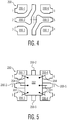
- Fig. 4 depicts a top plan view of an embodiment of a leadframe 200 that connects to, or forms all of or a part of, the pads. Portions (200-1 - 200-6) of the leadframe in Fig. 4 are numbered to correspond to the numbered pads of Figs. 3A - 3C . For example, the numbered portions of the leadframe are electrically connected to the corresponding numbered pads.
- a semiconductor chip is physically attached to the leadframe by, for example, an adhesive, and conductive pads of the semiconductor chip are electrically connected to the leadframe by, for example, wire bonding.
- Fig. 5 depicts the leadframe 200 of Fig. 4 after a semiconductor chip 202 has been attached to the leadframe and conductive wires 204 have been connected between conductive pads of the semiconductor chip and the leadframe.
- the conductive wires electrically connect the conductive pads of the semiconductor chip to the leadframe and the leadframe is electrically connected to the respective pads of the packaged semiconductor device.
- the leadframe, semiconductor chip, and wire bonds are enclosed within, for example, an epoxy encapsulate that forms at least a portion of the package structure 102.
- Fig. 6 depicts an alternate layout of a flat no-lead packaged semiconductor device 300-1 that includes two equilateral triangular pads 320 and four polygonal (e.g., trapezoidal) pads 324 oriented similar to that of Figs. 1A - 3C .
- the layout of Fig. 6 is arranged such that opposite vertices of the two triangular pads are nearest to the longest edges of the rectangular boundary.
- Fig. 7 depicts another alternate layout of a flat no-lead packaged semiconductor device 300-2 that includes two equilateral triangular pads 320 and four polygonal (e.g., trapezoidal) pads 324 oriented similar to that of Figs. 1A - 3C .
- the arrangement of Fig. 7 is similar to the arrangement of Fig. 3A , with slightly different arrangements of the polygonal pads.
- FIG. 8A and 8B depict top and bottom perspective views of a semiconductor device 400 with eight pads that has been packaged using a flat no-lead technique in accordance with an embodiment of the invention.
- the packaged semiconductor device is an eight pad flat no-lead packaged semiconductor device with dimensions of approximately 1.3 mm x 0.8 mm x 0.35 mm (length x width x height) that includes two interior pads and six edge pads.
- Figs. 8A and 8B depict top and bottom perspective views of a semiconductor device 400 with eight pads that has been packaged using a flat no-lead technique in accordance with an embodiment of the invention.
- the packaged semiconductor device is an eight pad flat no-lead packaged semiconductor device with dimensions of approximately 1.3 mm x 0.8 mm x 0.35 mm (length x width x height) that includes two interior pads and six edge pads.
- the two interior pads e.g., quadrilateral pads
- the six edge pads e.g., six polygonal pads
- each of the interior polygonal pads is located approximately in the center between four of the six edge pads and is configured such that a line running through at least one vertex of each of the interior polygonal pads is parallel to an edge of the rectangular boundary of the package structure.
- the configuration of the two interior polygonal pads and the six exterior polygonal pads exhibits a large pitch, e.g., approximately 0.4 mm, and a separation distance of around 0.2 mm.
- the eight pad flat no-lead packaged semiconductor device provides pad separation distances that are wide enough to prevent shorting between the pads while still providing enough surface area to enable reliable connection to a printed circuit board.
- Fig. 8A is a top perspective view of the eight pad flat no-lead packaged semiconductor device 400 that depicts a package structure 402 with a top major surface 404 and two side surfaces 406 and 408.
- the top surface typically includes markings such as product markings, although no marking are shown here.
- portions of the pads 424 and/or corresponding leadframe 500 are exposed at the side surfaces of the flat no-lead packaged semiconductor device.
- Fig. 8B is a bottom perspective view of the eight pad flat no-lead packaged semiconductor device 400 that depicts a bottom major surface 410 and two side surfaces 406 and 408 of the package structure 402.
- two interior polygonal pads 420 and six edge polygonal pads 424 are exposed at the bottom surface of the flat no-lead packaged semiconductor device.
- the combination of the two interior polygonal pads and the four edge polygonal pads arranged as shown in Fig. 8B provides an eight pad layout that optimizes the separation distances between the eight pads. Specifics of the pad layout are described in more detail below with reference to Figs. 9 and 10A - 10C .
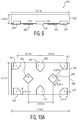
- Fig. 9 is a side view of the flat no-lead packaged semiconductor device 400 of Figs. 8A and 8B that depicts the height dimension and the length dimension of the flat no-lead packaged semiconductor device.
- the height dimension is 0.35 mm and the length dimension is 1.3 mm.
- Fig. 9 also illustrates that the pads 420 and 424 may protrude from a plane defined by the bottom major surface 404 of the package structure 402 of the flat no-lead packaged semiconductor device 400.
- the pads may protrude up to 20 micrometers from the bottom major surface of the package structure.
- the pads do not protrude from the bottom major surface of the package structure, e.g., the pads are flush with the bottom major surface of the package structure.
- Fig. 10A depicts a plan view of the bottom surface 410 of the flat no-lead packaged semiconductor device 400 that shows an embodiment of a layout of the eight pads, including the two interior polygonal pads 420 identified as pads 4 and 8 and six edge polygonal pads 424 identified as pads 1, 2, 3, 5, 6, and 7.
- pad 8 is a ground pad for connection to a ground terminal
- pad 4 is a Vcc pad for connection to a Vcc terminal, although other arrangements are possible.
- the basic dimensions of the flat no-lead packaged semiconductor device are described first followed by a description of the orientation of the pads. As shown in Fig.
- the bottom surface has a rectangular boundary of approximately 1.3 mm x 0.8 mm (e.g., length x width), the two interior polygonal pads are quadrilateral pads having sides of approximately 0.2 mm, and the centers of the two interior quadrilateral pads are separated from each other by approximately 0.5 mm. In an embodiment, the dimensions of the pads and separations distances are within ⁇ 0.05 mm.
- the two interior polygonal pads 420 are located on the horizontal centerline 430 that runs through the bottom surface 410.
- the two interior quadrilateral pads are oriented such that two vertices of each quadrilateral pad are located on the horizontal centerline.
- each of the two quadrilateral pads is oriented such that a line running through two vertices of the respective pad is parallel to the vertical centerline 432 of the bottom surface.
- the six edge polygonal pads 424 are located at the edge of the rectangular boundary with four of the edge polygonal pads being located in the vicinity of the corners of the rectangular boundary and referred to as "corner pads,” and the other two edge polygonal pads being located on an edge and equidistant between the two interior polygonal pads 420 and referred to as "intermediate edge pads.” As shown in Fig. 10A , each of the two interior quadrilateral pads is approximately centered between four edge polygonal pads, with two of the four edge pads being the corner pads and two of the four pads being the two intermediate edge pads.
- each of the interior quadrilateral pads has a first side that is parallel to a facing side of the edge polygonal pad that is nearest to the first side, a second side that is parallel to a facing side of the edge polygonal pad that is nearest to the second side, a third side that is parallel to a facing side of the edge polygonal pad that is nearest to the third side, and a fourth side that is parallel to a facing side of the edge polygonal pad that is nearest to the fourth side.
- interior pad 1 has a first side that is parallel to the facing side of edge polygonal pad 2, a second side that is parallel to the facing side of edge polygonal pad 3, a third side that is parallel to the facing side of edge polygonal pad 7, and a fourth side that is parallel to the facing side of edge polygonal pad 8.
- the parallel arrangement of the various sides of the pads is described with reference to Figs. 10B and 10C .
- Fig. 10B depicts the bottom surface 410 of the packaged semiconductor device 400 of Fig. 10A , with parallel lines 440A - 440H running from the lower left to the upper right to indicate parallel sides of the pads 420 and 424.
- edge polygonal pads 2, 3, 6, and 7 each have an inner side that is parallel to two sides of each of the two inner polygonal pads.
- Fig. 10C depicts the bottom surface 410 of the packaged semiconductor device 400 of Fig. 10A , with parallel lines 442A - 442H running from the lower right to the upper left to indicate parallel sides of the pads 420 and 424.
- edge polygonal pads 3, 4, 7, and 8 each have an inner side that is parallel to two sides of each of the two inner polygonal pads.
- the pad layout as shown in Figs. 8B and 10A - 10C depicts the pads 420 and 424 as exposed at the bottom surface 410 of the flat no-lead packaged semiconductor device 400.
- the packaged semiconductor device 400 includes a leadframe 500 that electrically connects the packaged semiconductor chip (not shown) to the eight pads 420 and 424.
- the interior polygonal pads are electrically connected to electrically conductive pins of the packaged semiconductor device as either ground, Vcc, or input/output pads. That is, the interior polygonal pads are not provided as a heat sink.
- the above-described layouts include packaged semiconductor devices with six and eight exposed pads, packaged semiconductor devices with other numbers of exposed pads are possible.
- the interior polygonal pads are described as equilateral triangular pads and quadrilateral pads, other shaped pads are possible. For example, triangular pads, which are not equilateral triangular pads, are possible.
- certain sides are described as being parallel to each other, it is possible that the similarly arranged but non-parallel sides may be utilized.
- certain dimensions are provided, other dimensions of any of the elements of the flat no-lead packaged semiconductor devices are possible. Additionally, although certain dimensions are noted, in some embodiments, the dimensions may vary within certain tolerances as are known in the field.
- a monolithic leadframe structure is utilized to form the leadframe that connects directly to the semiconductor chip and to form the pads.
- the leadframe is formed by etching the leadframe from the top side and from the bottom side to generate a different layout on the top side and the bottom side of the leadframe.
- the two equilateral triangular pads may have side dimensions of approximately 0.25 mm and the opposite side of each of the four trapezoidal pads is separated from a nearest parallel side of one of the two equilateral triangular pads by approximately 0.2 mm.
Landscapes
- Lead Frames For Integrated Circuits (AREA)
- Wire Bonding (AREA)
Claims (4)
- Halbleitervorrichtung, umfassend:einen Halbleiterchip (202);eine Gehäusestruktur (102), die eine rechteckige Umgrenzung definiert und eine Bodenfläche (110) aufweist und Folgendes umfasst:lediglich zwei innere dreieckige Kontaktflächen (120, 320), die an der Bodenfläche (110) der Gehäusestruktur (102) freiliegen, wobei die inneren dreieckigen Kontaktflächen jeweils voneinander getrennt sind und sich auf einer Achse (130, 132) der Bodenfläche (110) der Gehäusestruktur (102) befinden; undlediglich vier polygonale Kantenkontaktflächen (124, 324), die an der Bodenfläche (110) der Gehäusestruktur (102) freiliegen, wobei sich jede der polygonalen Kantenkontaktflächen (124, 324) an einer Kante der rechteckigen Umgrenzung befindet, wobei die polygonalen Kantenkontaktflächen (124, 324) eine polygonale Kantenkontaktfläche in der Nähe jeder Ecke der rechteckigen Umgrenzung beinhalten;wobei jede der inneren dreieckigen Kontaktflächen (120, 320) eine erste Seite, die zu einer gegenüberliegenden Seite der polygonalen Kantenkontaktfläche, die der ersten Seite am nächsten ist, parallel (140A-140D) ist, und eine zweite Seite, die zu einer gegenüberliegenden Seite der polygonalen Kantenkontaktfläche, die der zweiten Seite am nächsten ist, parallel (142A-142D) ist, aufweist; undwobei die inneren dreieckigen Kontaktflächen (120, 320) so konfiguriert sind, dass eine Linie (130, 132), die zwischen mindestens einem Eckpunkt jeder der inneren dreieckigen Kontaktflächen (120, 320) verläuft, zu einer Kante der rechteckigen Umgrenzung der Gehäusestruktur (102) parallel ist,wobei die inneren dreieckigen Kontaktflächen (120, 320) ferner so konfiguriert sind, dass eine Linie (130, 132), die durch einen Eckpunkt jeder der inneren dreieckigen Kontaktflächen (120, 320) verläuft, zu einer Kante der rechteckigen Umgrenzung der Gehäusestruktur (102) parallel ist.
- Halbleitervorrichtung nach Anspruch 1, wobei die Linie, die durch einen Eckpunkt jeder der inneren dreieckigen Kontaktflächen (120, 320) verläuft, eine Achse (130, 132) der rechteckigen Umgrenzung der Gehäusestruktur (102) ist.
- Halbleitervorrichtung nach Anspruch 1, wobei die zwei inneren dreieckigen Kontaktflächen (120, 320) zwei gleichseitige dreieckige Kontaktflächen sind.
- Halbleitervorrichtung nach Anspruch 1, wobei die dreieckigen polygonalen Kontaktflächen (120, 320) Seitenabmessungen von 0,15 mm - 0,25 mm aufweisen und wobei der Abstand der inneren dreieckigen Kontaktflächen (120, 320) ungefähr 0,4 mm beträgt.
Applications Claiming Priority (1)
| Application Number | Priority Date | Filing Date | Title |
|---|---|---|---|
| US14/099,768 US9269690B2 (en) | 2013-12-06 | 2013-12-06 | Packaged semiconductor device with interior polygonal pads |
Publications (3)
| Publication Number | Publication Date |
|---|---|
| EP2881984A2 EP2881984A2 (de) | 2015-06-10 |
| EP2881984A3 EP2881984A3 (de) | 2015-07-08 |
| EP2881984B1 true EP2881984B1 (de) | 2019-03-13 |
Family
ID=51662003
Family Applications (1)
| Application Number | Title | Priority Date | Filing Date |
|---|---|---|---|
| EP14188355.3A Active EP2881984B1 (de) | 2013-12-06 | 2014-10-09 | Verkapselte Vorrichtung mit inneren polygonalen Pads |
Country Status (3)
| Country | Link |
|---|---|
| US (2) | US9269690B2 (de) |
| EP (1) | EP2881984B1 (de) |
| CN (1) | CN104701286B (de) |
Cited By (2)
| Publication number | Priority date | Publication date | Assignee | Title |
|---|---|---|---|---|
| US20250006510A1 (en) * | 2023-06-30 | 2025-01-02 | Texas Instruments Incorporated | Semiconductor device package with wettable flanks |
| DE102019118705B4 (de) | 2018-07-18 | 2026-04-02 | Xerox Corporation | Gedruckte elektronische vorrichtungen, die eine verbesserte leistung aufweisen und mehrere elektrische vorrichtungen, sowie verfahren zur herstellung und verfahren zur verwendung |
Families Citing this family (7)
| Publication number | Priority date | Publication date | Assignee | Title |
|---|---|---|---|---|
| CN106469689B (zh) * | 2015-08-21 | 2019-10-11 | 安世有限公司 | 电子元件及其形成方法 |
| US11056435B2 (en) * | 2017-11-16 | 2021-07-06 | Advanced Semiconductor Engineering, Inc. | Semiconductor package with chamfered pads |
| CN212303653U (zh) * | 2020-03-26 | 2021-01-05 | 北京小米移动软件有限公司 | 芯片、电路板、电路板组件及电子设备 |
| CN113921491A (zh) * | 2020-07-08 | 2022-01-11 | 北京小米移动软件有限公司 | 芯片、电路板及电子设备 |
| US11855001B2 (en) * | 2020-11-04 | 2023-12-26 | Texas Instruments Incorporated | Leadless leadframe and semiconductor device package therefrom |
| WO2022164574A1 (en) * | 2021-01-29 | 2022-08-04 | Microchip Technology Incorporated | Lead frames for semiconductor packages with increased reliability and related packages and methods |
| US11430718B2 (en) | 2021-01-29 | 2022-08-30 | Microchip Technology Incorporated | Lead frames for semiconductor packages with increased reliability and related semiconductor device packages and methods |
Family Cites Families (14)
| Publication number | Priority date | Publication date | Assignee | Title |
|---|---|---|---|---|
| US5340772A (en) * | 1992-07-17 | 1994-08-23 | Lsi Logic Corporation | Method of increasing the layout efficiency of dies on a wafer and increasing the ratio of I/O area to active area per die |
| US8330270B1 (en) * | 1998-06-10 | 2012-12-11 | Utac Hong Kong Limited | Integrated circuit package having a plurality of spaced apart pad portions |
| US6597059B1 (en) * | 2001-04-04 | 2003-07-22 | Amkor Technology, Inc. | Thermally enhanced chip scale lead on chip semiconductor package |
| US6841854B2 (en) * | 2002-04-01 | 2005-01-11 | Matsushita Electric Industrial Co., Ltd. | Semiconductor device |
| JP2004071670A (ja) * | 2002-08-02 | 2004-03-04 | Fuji Photo Film Co Ltd | Icパッケージ、接続構造、および電子機器 |
| US7262491B2 (en) * | 2005-09-06 | 2007-08-28 | Advanced Interconnect Technologies Limited | Die pad for semiconductor packages and methods of making and using same |
| US7714415B2 (en) * | 2006-04-28 | 2010-05-11 | Intersil Americas, Inc. | Leadframe structures for semiconductor packages |
| EP2130223A1 (de) | 2007-02-14 | 2009-12-09 | Nxp B.V. | Zwei- oder mehrreihige verpackung |
| JP5649277B2 (ja) * | 2008-12-22 | 2015-01-07 | ローム株式会社 | 半導体装置 |
| CN102428558B (zh) | 2009-05-15 | 2014-06-25 | 罗姆股份有限公司 | 半导体装置 |
| CN102484083A (zh) | 2009-09-11 | 2012-05-30 | 罗姆股份有限公司 | 半导体装置及其制造方法 |
| JP5220714B2 (ja) * | 2009-09-18 | 2013-06-26 | セイコーインスツル株式会社 | 樹脂封止型半導体装置及びその製造方法 |
| US8836107B2 (en) | 2011-02-24 | 2014-09-16 | Texas Instruments Incorporated | High pin count, small SON/QFN packages having heat-dissipating pad |
| US20130133193A1 (en) | 2011-11-28 | 2013-05-30 | Mediatek Singapore Pte. Ltd. | Surface mount technology process for advanced quad flat no-lead package process and stencil used therewith |
-
2013
- 2013-12-06 US US14/099,768 patent/US9269690B2/en active Active
-
2014
- 2014-10-09 EP EP14188355.3A patent/EP2881984B1/de active Active
- 2014-11-14 CN CN201410646188.7A patent/CN104701286B/zh active Active
-
2016
- 2016-01-07 US US14/990,304 patent/US10056343B2/en active Active
Non-Patent Citations (1)
| Title |
|---|
| None * |
Cited By (2)
| Publication number | Priority date | Publication date | Assignee | Title |
|---|---|---|---|---|
| DE102019118705B4 (de) | 2018-07-18 | 2026-04-02 | Xerox Corporation | Gedruckte elektronische vorrichtungen, die eine verbesserte leistung aufweisen und mehrere elektrische vorrichtungen, sowie verfahren zur herstellung und verfahren zur verwendung |
| US20250006510A1 (en) * | 2023-06-30 | 2025-01-02 | Texas Instruments Incorporated | Semiconductor device package with wettable flanks |
Also Published As
| Publication number | Publication date |
|---|---|
| US9269690B2 (en) | 2016-02-23 |
| CN104701286A (zh) | 2015-06-10 |
| EP2881984A2 (de) | 2015-06-10 |
| US10056343B2 (en) | 2018-08-21 |
| US20150162298A1 (en) | 2015-06-11 |
| EP2881984A3 (de) | 2015-07-08 |
| CN104701286B (zh) | 2018-05-01 |
| US20160118357A1 (en) | 2016-04-28 |
Similar Documents
| Publication | Publication Date | Title |
|---|---|---|
| EP2881984B1 (de) | Verkapselte Vorrichtung mit inneren polygonalen Pads | |
| US7646083B2 (en) | I/O connection scheme for QFN leadframe and package structures | |
| US7245007B1 (en) | Exposed lead interposer leadframe package | |
| CN101350318B (zh) | 电子封装及电子装置 | |
| TWI792588B (zh) | 半導體封裝 | |
| US9379071B2 (en) | Single inline no-lead semiconductor package | |
| EP3758060A1 (de) | Mehrreihiges qfn-halbleitergehäuse | |
| JP6636846B2 (ja) | 半導体装置および半導体装置の製造方法 | |
| WO2015080000A1 (ja) | 半導体装置および半導体装置の製造方法 | |
| KR100652106B1 (ko) | 회로 장치 | |
| US12074098B2 (en) | Three-dimensional functional integration | |
| CN104810345A (zh) | 无引线封装式功率半导体模块 | |
| KR100379089B1 (ko) | 리드프레임 및 이를 이용한 반도체패키지 | |
| US9324643B1 (en) | Integrated circuit device having exposed contact pads and leads supporting the integrated circuit die and method of forming the device | |
| KR20110123505A (ko) | 반도체 패키지 | |
| KR20150053916A (ko) | 이중 로우 쿼드 플랫 노-리드 반도체 패키지 | |
| TWI582905B (zh) | 晶片封裝結構及其製作方法 | |
| CN103681387B (zh) | 制造半导体器件的方法 | |
| CN102931150B (zh) | 无外引脚封装结构 | |
| JP2990645B2 (ja) | 半導体集積回路用リードフレームおよび半導体集積回路 | |
| CN102024778B (zh) | 导线架及芯片封装体 | |
| CN220400583U (zh) | 一种半导体引线框架及半导体封装器件 | |
| US8304865B2 (en) | Leadframe and chip package | |
| KR100235498B1 (ko) | 반도체 패키지 | |
| KR100668932B1 (ko) | 리드프레임 및 이를 이용한 반도체패키지 |
Legal Events
| Date | Code | Title | Description |
|---|---|---|---|
| PUAL | Search report despatched |
Free format text: ORIGINAL CODE: 0009013 |
|
| PUAI | Public reference made under article 153(3) epc to a published international application that has entered the european phase |
Free format text: ORIGINAL CODE: 0009012 |
|
| 17P | Request for examination filed |
Effective date: 20141009 |
|
| AK | Designated contracting states |
Kind code of ref document: A2 Designated state(s): AL AT BE BG CH CY CZ DE DK EE ES FI FR GB GR HR HU IE IS IT LI LT LU LV MC MK MT NL NO PL PT RO RS SE SI SK SM TR |
|
| AX | Request for extension of the european patent |
Extension state: BA ME |
|
| AK | Designated contracting states |
Kind code of ref document: A3 Designated state(s): AL AT BE BG CH CY CZ DE DK EE ES FI FR GB GR HR HU IE IS IT LI LT LU LV MC MK MT NL NO PL PT RO RS SE SI SK SM TR |
|
| AX | Request for extension of the european patent |
Extension state: BA ME |
|
| RIC1 | Information provided on ipc code assigned before grant |
Ipc: H01L 23/00 20060101ALI20150604BHEP Ipc: H01L 23/31 20060101AFI20150604BHEP Ipc: H01L 23/495 20060101ALI20150604BHEP |
|
| R17P | Request for examination filed (corrected) |
Effective date: 20160108 |
|
| RBV | Designated contracting states (corrected) |
Designated state(s): AL AT BE BG CH CY CZ DE DK EE ES FI FR GB GR HR HU IE IS IT LI LT LU LV MC MK MT NL NO PL PT RO RS SE SI SK SM TR |
|
| STAA | Information on the status of an ep patent application or granted ep patent |
Free format text: STATUS: EXAMINATION IS IN PROGRESS |
|
| 17Q | First examination report despatched |
Effective date: 20170127 |
|
| RAP1 | Party data changed (applicant data changed or rights of an application transferred) |
Owner name: NEXPERIA B.V. |
|
| GRAP | Despatch of communication of intention to grant a patent |
Free format text: ORIGINAL CODE: EPIDOSNIGR1 |
|
| STAA | Information on the status of an ep patent application or granted ep patent |
Free format text: STATUS: GRANT OF PATENT IS INTENDED |
|
| INTG | Intention to grant announced |
Effective date: 20181030 |
|
| GRAS | Grant fee paid |
Free format text: ORIGINAL CODE: EPIDOSNIGR3 |
|
| GRAA | (expected) grant |
Free format text: ORIGINAL CODE: 0009210 |
|
| STAA | Information on the status of an ep patent application or granted ep patent |
Free format text: STATUS: THE PATENT HAS BEEN GRANTED |
|
| AK | Designated contracting states |
Kind code of ref document: B1 Designated state(s): AL AT BE BG CH CY CZ DE DK EE ES FI FR GB GR HR HU IE IS IT LI LT LU LV MC MK MT NL NO PL PT RO RS SE SI SK SM TR |
|
| REG | Reference to a national code |
Ref country code: GB Ref legal event code: FG4D |
|
| REG | Reference to a national code |
Ref country code: CH Ref legal event code: EP Ref country code: AT Ref legal event code: REF Ref document number: 1108865 Country of ref document: AT Kind code of ref document: T Effective date: 20190315 |
|
| REG | Reference to a national code |
Ref country code: IE Ref legal event code: FG4D |
|
| REG | Reference to a national code |
Ref country code: DE Ref legal event code: R096 Ref document number: 602014042717 Country of ref document: DE |
|
| REG | Reference to a national code |
Ref country code: NL Ref legal event code: MP Effective date: 20190313 |
|
| REG | Reference to a national code |
Ref country code: LT Ref legal event code: MG4D |
|
| PG25 | Lapsed in a contracting state [announced via postgrant information from national office to epo] |
Ref country code: SE Free format text: LAPSE BECAUSE OF FAILURE TO SUBMIT A TRANSLATION OF THE DESCRIPTION OR TO PAY THE FEE WITHIN THE PRESCRIBED TIME-LIMIT Effective date: 20190313 Ref country code: LT Free format text: LAPSE BECAUSE OF FAILURE TO SUBMIT A TRANSLATION OF THE DESCRIPTION OR TO PAY THE FEE WITHIN THE PRESCRIBED TIME-LIMIT Effective date: 20190313 Ref country code: NO Free format text: LAPSE BECAUSE OF FAILURE TO SUBMIT A TRANSLATION OF THE DESCRIPTION OR TO PAY THE FEE WITHIN THE PRESCRIBED TIME-LIMIT Effective date: 20190613 Ref country code: FI Free format text: LAPSE BECAUSE OF FAILURE TO SUBMIT A TRANSLATION OF THE DESCRIPTION OR TO PAY THE FEE WITHIN THE PRESCRIBED TIME-LIMIT Effective date: 20190313 |
|
| PG25 | Lapsed in a contracting state [announced via postgrant information from national office to epo] |
Ref country code: LV Free format text: LAPSE BECAUSE OF FAILURE TO SUBMIT A TRANSLATION OF THE DESCRIPTION OR TO PAY THE FEE WITHIN THE PRESCRIBED TIME-LIMIT Effective date: 20190313 Ref country code: BG Free format text: LAPSE BECAUSE OF FAILURE TO SUBMIT A TRANSLATION OF THE DESCRIPTION OR TO PAY THE FEE WITHIN THE PRESCRIBED TIME-LIMIT Effective date: 20190613 Ref country code: RS Free format text: LAPSE BECAUSE OF FAILURE TO SUBMIT A TRANSLATION OF THE DESCRIPTION OR TO PAY THE FEE WITHIN THE PRESCRIBED TIME-LIMIT Effective date: 20190313 Ref country code: HR Free format text: LAPSE BECAUSE OF FAILURE TO SUBMIT A TRANSLATION OF THE DESCRIPTION OR TO PAY THE FEE WITHIN THE PRESCRIBED TIME-LIMIT Effective date: 20190313 Ref country code: GR Free format text: LAPSE BECAUSE OF FAILURE TO SUBMIT A TRANSLATION OF THE DESCRIPTION OR TO PAY THE FEE WITHIN THE PRESCRIBED TIME-LIMIT Effective date: 20190614 Ref country code: NL Free format text: LAPSE BECAUSE OF FAILURE TO SUBMIT A TRANSLATION OF THE DESCRIPTION OR TO PAY THE FEE WITHIN THE PRESCRIBED TIME-LIMIT Effective date: 20190313 |
|
| REG | Reference to a national code |
Ref country code: AT Ref legal event code: MK05 Ref document number: 1108865 Country of ref document: AT Kind code of ref document: T Effective date: 20190313 |
|
| PG25 | Lapsed in a contracting state [announced via postgrant information from national office to epo] |
Ref country code: PT Free format text: LAPSE BECAUSE OF FAILURE TO SUBMIT A TRANSLATION OF THE DESCRIPTION OR TO PAY THE FEE WITHIN THE PRESCRIBED TIME-LIMIT Effective date: 20190713 Ref country code: AL Free format text: LAPSE BECAUSE OF FAILURE TO SUBMIT A TRANSLATION OF THE DESCRIPTION OR TO PAY THE FEE WITHIN THE PRESCRIBED TIME-LIMIT Effective date: 20190313 Ref country code: ES Free format text: LAPSE BECAUSE OF FAILURE TO SUBMIT A TRANSLATION OF THE DESCRIPTION OR TO PAY THE FEE WITHIN THE PRESCRIBED TIME-LIMIT Effective date: 20190313 Ref country code: SK Free format text: LAPSE BECAUSE OF FAILURE TO SUBMIT A TRANSLATION OF THE DESCRIPTION OR TO PAY THE FEE WITHIN THE PRESCRIBED TIME-LIMIT Effective date: 20190313 Ref country code: CZ Free format text: LAPSE BECAUSE OF FAILURE TO SUBMIT A TRANSLATION OF THE DESCRIPTION OR TO PAY THE FEE WITHIN THE PRESCRIBED TIME-LIMIT Effective date: 20190313 Ref country code: RO Free format text: LAPSE BECAUSE OF FAILURE TO SUBMIT A TRANSLATION OF THE DESCRIPTION OR TO PAY THE FEE WITHIN THE PRESCRIBED TIME-LIMIT Effective date: 20190313 Ref country code: IT Free format text: LAPSE BECAUSE OF FAILURE TO SUBMIT A TRANSLATION OF THE DESCRIPTION OR TO PAY THE FEE WITHIN THE PRESCRIBED TIME-LIMIT Effective date: 20190313 Ref country code: EE Free format text: LAPSE BECAUSE OF FAILURE TO SUBMIT A TRANSLATION OF THE DESCRIPTION OR TO PAY THE FEE WITHIN THE PRESCRIBED TIME-LIMIT Effective date: 20190313 |
|
| PG25 | Lapsed in a contracting state [announced via postgrant information from national office to epo] |
Ref country code: PL Free format text: LAPSE BECAUSE OF FAILURE TO SUBMIT A TRANSLATION OF THE DESCRIPTION OR TO PAY THE FEE WITHIN THE PRESCRIBED TIME-LIMIT Effective date: 20190313 Ref country code: SM Free format text: LAPSE BECAUSE OF FAILURE TO SUBMIT A TRANSLATION OF THE DESCRIPTION OR TO PAY THE FEE WITHIN THE PRESCRIBED TIME-LIMIT Effective date: 20190313 |
|
| REG | Reference to a national code |
Ref country code: DE Ref legal event code: R097 Ref document number: 602014042717 Country of ref document: DE |
|
| PG25 | Lapsed in a contracting state [announced via postgrant information from national office to epo] |
Ref country code: IS Free format text: LAPSE BECAUSE OF FAILURE TO SUBMIT A TRANSLATION OF THE DESCRIPTION OR TO PAY THE FEE WITHIN THE PRESCRIBED TIME-LIMIT Effective date: 20190713 Ref country code: AT Free format text: LAPSE BECAUSE OF FAILURE TO SUBMIT A TRANSLATION OF THE DESCRIPTION OR TO PAY THE FEE WITHIN THE PRESCRIBED TIME-LIMIT Effective date: 20190313 |
|
| PLBE | No opposition filed within time limit |
Free format text: ORIGINAL CODE: 0009261 |
|
| STAA | Information on the status of an ep patent application or granted ep patent |
Free format text: STATUS: NO OPPOSITION FILED WITHIN TIME LIMIT |
|
| PG25 | Lapsed in a contracting state [announced via postgrant information from national office to epo] |
Ref country code: DK Free format text: LAPSE BECAUSE OF FAILURE TO SUBMIT A TRANSLATION OF THE DESCRIPTION OR TO PAY THE FEE WITHIN THE PRESCRIBED TIME-LIMIT Effective date: 20190313 |
|
| 26N | No opposition filed |
Effective date: 20191216 |
|
| PG25 | Lapsed in a contracting state [announced via postgrant information from national office to epo] |
Ref country code: SI Free format text: LAPSE BECAUSE OF FAILURE TO SUBMIT A TRANSLATION OF THE DESCRIPTION OR TO PAY THE FEE WITHIN THE PRESCRIBED TIME-LIMIT Effective date: 20190313 |
|
| PG25 | Lapsed in a contracting state [announced via postgrant information from national office to epo] |
Ref country code: TR Free format text: LAPSE BECAUSE OF FAILURE TO SUBMIT A TRANSLATION OF THE DESCRIPTION OR TO PAY THE FEE WITHIN THE PRESCRIBED TIME-LIMIT Effective date: 20190313 |
|
| PG25 | Lapsed in a contracting state [announced via postgrant information from national office to epo] |
Ref country code: MC Free format text: LAPSE BECAUSE OF FAILURE TO SUBMIT A TRANSLATION OF THE DESCRIPTION OR TO PAY THE FEE WITHIN THE PRESCRIBED TIME-LIMIT Effective date: 20190313 |
|
| REG | Reference to a national code |
Ref country code: CH Ref legal event code: PL |
|
| PG25 | Lapsed in a contracting state [announced via postgrant information from national office to epo] |
Ref country code: LI Free format text: LAPSE BECAUSE OF NON-PAYMENT OF DUE FEES Effective date: 20191031 Ref country code: LU Free format text: LAPSE BECAUSE OF NON-PAYMENT OF DUE FEES Effective date: 20191009 Ref country code: CH Free format text: LAPSE BECAUSE OF NON-PAYMENT OF DUE FEES Effective date: 20191031 |
|
| REG | Reference to a national code |
Ref country code: BE Ref legal event code: MM Effective date: 20191031 |
|
| PG25 | Lapsed in a contracting state [announced via postgrant information from national office to epo] |
Ref country code: BE Free format text: LAPSE BECAUSE OF NON-PAYMENT OF DUE FEES Effective date: 20191031 |
|
| GBPC | Gb: european patent ceased through non-payment of renewal fee |
Effective date: 20191009 |
|
| PG25 | Lapsed in a contracting state [announced via postgrant information from national office to epo] |
Ref country code: FR Free format text: LAPSE BECAUSE OF NON-PAYMENT OF DUE FEES Effective date: 20191031 Ref country code: GB Free format text: LAPSE BECAUSE OF NON-PAYMENT OF DUE FEES Effective date: 20191009 Ref country code: IE Free format text: LAPSE BECAUSE OF NON-PAYMENT OF DUE FEES Effective date: 20191009 |
|
| PG25 | Lapsed in a contracting state [announced via postgrant information from national office to epo] |
Ref country code: CY Free format text: LAPSE BECAUSE OF FAILURE TO SUBMIT A TRANSLATION OF THE DESCRIPTION OR TO PAY THE FEE WITHIN THE PRESCRIBED TIME-LIMIT Effective date: 20190313 |
|
| PG25 | Lapsed in a contracting state [announced via postgrant information from national office to epo] |
Ref country code: HU Free format text: LAPSE BECAUSE OF FAILURE TO SUBMIT A TRANSLATION OF THE DESCRIPTION OR TO PAY THE FEE WITHIN THE PRESCRIBED TIME-LIMIT; INVALID AB INITIO Effective date: 20141009 Ref country code: MT Free format text: LAPSE BECAUSE OF FAILURE TO SUBMIT A TRANSLATION OF THE DESCRIPTION OR TO PAY THE FEE WITHIN THE PRESCRIBED TIME-LIMIT Effective date: 20190313 |
|
| PG25 | Lapsed in a contracting state [announced via postgrant information from national office to epo] |
Ref country code: MK Free format text: LAPSE BECAUSE OF FAILURE TO SUBMIT A TRANSLATION OF THE DESCRIPTION OR TO PAY THE FEE WITHIN THE PRESCRIBED TIME-LIMIT Effective date: 20190313 |
|
| REG | Reference to a national code |
Ref country code: DE Ref legal event code: R079 Ref document number: 602014042717 Country of ref document: DE Free format text: PREVIOUS MAIN CLASS: H01L0023310000 Ipc: H10W0074100000 |
|
| PGFP | Annual fee paid to national office [announced via postgrant information from national office to epo] |
Ref country code: DE Payment date: 20251028 Year of fee payment: 12 |