EP2880693B1 - Photokathode mit einem siliciumsubstrat mit einer borschicht - Google Patents
Photokathode mit einem siliciumsubstrat mit einer borschicht Download PDFInfo
- Publication number
- EP2880693B1 EP2880693B1 EP13825872.8A EP13825872A EP2880693B1 EP 2880693 B1 EP2880693 B1 EP 2880693B1 EP 13825872 A EP13825872 A EP 13825872A EP 2880693 B1 EP2880693 B1 EP 2880693B1
- Authority
- EP
- European Patent Office
- Prior art keywords
- photocathode
- layer
- sensor
- silicon
- silicon substrate
- Prior art date
- Legal status (The legal status is an assumption and is not a legal conclusion. Google has not performed a legal analysis and makes no representation as to the accuracy of the status listed.)
- Active
Links
Images




Classifications
-
- H—ELECTRICITY
- H01—ELECTRIC ELEMENTS
- H01J—ELECTRIC DISCHARGE TUBES OR DISCHARGE LAMPS
- H01J29/00—Details of cathode-ray tubes or of electron-beam tubes of the types covered by group H01J31/00
- H01J29/02—Electrodes; Screens; Mounting, supporting, spacing or insulating thereof
- H01J29/10—Screens on or from which an image or pattern is formed, picked up, converted or stored
- H01J29/36—Photoelectric screens; Charge-storage screens
- H01J29/38—Photoelectric screens; Charge-storage screens not using charge storage, e.g. photo-emissive screen, extended cathode
- H01J29/385—Photocathodes comprising a layer which modified the wave length of impinging radiation
-
- G—PHYSICS
- G01—MEASURING; TESTING
- G01N—INVESTIGATING OR ANALYSING MATERIALS BY DETERMINING THEIR CHEMICAL OR PHYSICAL PROPERTIES
- G01N21/00—Investigating or analysing materials by the use of optical means, i.e. using sub-millimetre waves, infrared, visible or ultraviolet light
- G01N21/84—Systems specially adapted for particular applications
- G01N21/88—Investigating the presence of flaws or contamination
- G01N21/95—Investigating the presence of flaws or contamination characterised by the material or shape of the object to be examined
- G01N21/9501—Semiconductor wafers
-
- G—PHYSICS
- G02—OPTICS
- G02B—OPTICAL ELEMENTS, SYSTEMS OR APPARATUS
- G02B21/00—Microscopes
- G02B21/06—Means for illuminating specimens
- G02B21/08—Condensers
- G02B21/12—Condensers affording bright-field illumination
- G02B21/125—Condensers affording bright-field illumination affording both dark- and bright-field illumination
-
- H—ELECTRICITY
- H01—ELECTRIC ELEMENTS
- H01J—ELECTRIC DISCHARGE TUBES OR DISCHARGE LAMPS
- H01J1/00—Details of electrodes, of magnetic control means, of screens, or of the mounting or spacing thereof, common to two or more basic types of discharge tubes or lamps
- H01J1/02—Main electrodes
- H01J1/34—Photo-emissive cathodes
-
- H—ELECTRICITY
- H01—ELECTRIC ELEMENTS
- H01J—ELECTRIC DISCHARGE TUBES OR DISCHARGE LAMPS
- H01J31/00—Cathode ray tubes; Electron beam tubes
- H01J31/08—Cathode ray tubes; Electron beam tubes having a screen on or from which an image or pattern is formed, picked up, converted, or stored
- H01J31/26—Image pick-up tubes having an input of visible light and electric output
-
- H—ELECTRICITY
- H01—ELECTRIC ELEMENTS
- H01J—ELECTRIC DISCHARGE TUBES OR DISCHARGE LAMPS
- H01J31/00—Cathode ray tubes; Electron beam tubes
- H01J31/08—Cathode ray tubes; Electron beam tubes having a screen on or from which an image or pattern is formed, picked up, converted, or stored
- H01J31/50—Image-conversion or image-amplification tubes, i.e. having optical, X-ray, or analogous input, and optical output
-
- H—ELECTRICITY
- H10—SEMICONDUCTOR DEVICES; ELECTRIC SOLID-STATE DEVICES NOT OTHERWISE PROVIDED FOR
- H10F—INORGANIC SEMICONDUCTOR DEVICES SENSITIVE TO INFRARED RADIATION, LIGHT, ELECTROMAGNETIC RADIATION OF SHORTER WAVELENGTH OR CORPUSCULAR RADIATION
- H10F39/00—Integrated devices, or assemblies of multiple devices, comprising at least one element covered by group H10F30/00, e.g. radiation detectors comprising photodiode arrays
- H10F39/10—Integrated devices
- H10F39/12—Image sensors
- H10F39/15—Charge-coupled device [CCD] image sensors
-
- H—ELECTRICITY
- H10—SEMICONDUCTOR DEVICES; ELECTRIC SOLID-STATE DEVICES NOT OTHERWISE PROVIDED FOR
- H10F—INORGANIC SEMICONDUCTOR DEVICES SENSITIVE TO INFRARED RADIATION, LIGHT, ELECTROMAGNETIC RADIATION OF SHORTER WAVELENGTH OR CORPUSCULAR RADIATION
- H10F39/00—Integrated devices, or assemblies of multiple devices, comprising at least one element covered by group H10F30/00, e.g. radiation detectors comprising photodiode arrays
- H10F39/10—Integrated devices
- H10F39/12—Image sensors
- H10F39/15—Charge-coupled device [CCD] image sensors
- H10F39/159—Charge-coupled device [CCD] image sensors comprising a photoconductive layer deposited on the CCD structure
-
- H—ELECTRICITY
- H10—SEMICONDUCTOR DEVICES; ELECTRIC SOLID-STATE DEVICES NOT OTHERWISE PROVIDED FOR
- H10F—INORGANIC SEMICONDUCTOR DEVICES SENSITIVE TO INFRARED RADIATION, LIGHT, ELECTROMAGNETIC RADIATION OF SHORTER WAVELENGTH OR CORPUSCULAR RADIATION
- H10F39/00—Integrated devices, or assemblies of multiple devices, comprising at least one element covered by group H10F30/00, e.g. radiation detectors comprising photodiode arrays
- H10F39/10—Integrated devices
- H10F39/12—Image sensors
- H10F39/18—Complementary metal-oxide-semiconductor [CMOS] image sensors; Photodiode array image sensors
-
- H—ELECTRICITY
- H10—SEMICONDUCTOR DEVICES; ELECTRIC SOLID-STATE DEVICES NOT OTHERWISE PROVIDED FOR
- H10F—INORGANIC SEMICONDUCTOR DEVICES SENSITIVE TO INFRARED RADIATION, LIGHT, ELECTROMAGNETIC RADIATION OF SHORTER WAVELENGTH OR CORPUSCULAR RADIATION
- H10F39/00—Integrated devices, or assemblies of multiple devices, comprising at least one element covered by group H10F30/00, e.g. radiation detectors comprising photodiode arrays
- H10F39/80—Constructional details of image sensors
Definitions
- the present invention generally relates to low light sensing detectors (sensors) used in conjunction with semiconductor wafer, reticle or photomask inspection systems, and more particularly to photocathodes utilized in the sensors for such inspection systems.
- a photoelectron 62 When a photoelectron 62 has sufficient energy to escape through the output side of photocathode 54 (i.e., downward in the figure), it enters gap region 56. Because CCD 55 is at a positive potential, usually of 2kV or more, relative to photocathode 54, photoelectron 62 is accelerated towards CCD 55 such that it achieves an energy greater than about 2 keV, whereby photoelectrons will typically generate multiple electrons inside CCD 55. The electrons generated inside CCD 55 are then transmitted (e.g., by way of pins 57) to a processing system (not shown) that is configured to generate an associated image or other data associated with the detected photoelectrons.
- a processing system not shown
- Prior-art photocathodes require difficult tradeoffs between conflicting requirements associated with absorbing photons and emitting photoelectrons.
- a good photocathode needs to have a high probability of absorbing photons at wavelengths of interest, and a high probability of generating one (or more) photoelectrons from that absorbed photon.
- a good photocathode also needs to have a high probability that any photoelectron generated by an absorbed photon escapes from the photocathode.
- a thicker photocathode increases the probability that an incident photon will be absorbed, but also increases the probability that the resulting emitted photoelectron will recombine (i.e., be lost) before it escapes.
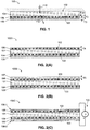
- Fig. 2(B) illustrates, in cross section view, a photocathode 100B according to a second alternative embodiment including a silicon substrate 101, a lower boron layer 104 disposed on output surface 103, a low work-function layer 105 disposed on boron layer 104, and an upper boron layer 106 disposed on illuminated surface 102.
- Photocathode 100B differs from the previously discussed embodiments in that it further includes one or more anti-reflection coating layers (fourth layer) 107 disposed on upper boron layer 106.
- Fig. 2(C) illustrates a photocathode 100C according to a third alternative embodiment including silicon substrate 101, lower boron layer 104 disposed on output surface 103, low work-function layer 105 disposed on boron layer 104, and upper boron layer 106 disposed on illuminated surface 102.
- Photocathode 100C differs from the previous embodiments in that an external voltage source 120 is connected to generate an external potential difference between illuminated surface 102 and output surface 103 in order to cause electrons generated in silicon substrate 101 to preferentially move towards output surface 103.
- output surface 103 is held at a positive potential relative to illuminated surface 102.
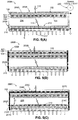
- Fig. 3 shows a cross-section view of a photocathode 100D according to another embodiment of the present invention in which gradients of dopants are purposefully diffused into substrate 101 from one or both of illuminated surface 102 and output surface 103 to direct photoelectrons within the silicon towards output surface 103.
- the low work function material layer is omitted for brevity.
- a thin boron silicide layer 126 is formed between the silicon and boron. Some of the boron will diffuse into silicon to form diffusion region 101-1 (indicated by shaded area), thereby creating a potential gradient that will tend to drive electrons away from illuminated surface 102 into substrate 101.
- sensor 200 includes conductive structures (e.g., similar to the grid structure described above with reference to Fig. 2(C) ) that are operably disposed on or adjacent to photocathode 100 and detection device 210 such that, when a suitable voltage supply 220 is operably coupled to sensor 200A, an electric field is generated between photocathode 100 and detection device 210 that serves to accelerate electrons 112 emitted from photocathode into gap region 206 toward detection device 210.
- output surface 103 of photocathode 100 is held at a potential of less than about 5 V positive relative to the illumination surface 102 by a second voltage source (not shown).
- a wafer, reticle or photomask inspection system including an illumination source (e.g., a laser system) for transmitting light (photons) onto a sample/wafer, a sensor (e.g., a photomultiplier, an image intensifier or an EBCCD) that utilizes any of the inventive photocathodes described above to detect photons passing through or reflected by the sample/wafer, and an associated optical system for guiding the light/photons from the illumination source to the sample (wafer, reticle or photomask), and from the sample to the sensor. Examples of these embodiments are shown in Figs. 6 through 10 .
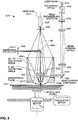
- Fig. 6 shows key components of an inspection system 300A with dark-field and bright field inspection modes.
- the optics utilized by system 300A comprise a high numerical aperture large field-of-view objective lens 128, tube lens 139 for setting or adjusting the magnification and a detector 200, which incorporates a photocathode constructed in accordance with any of the embodiments described above.
- the detector 200 incorporates the inventive photocathode in an EBCCD or image intensifier arrangement similar to that shown in any of Figs. 5(A) to 5(C) . More details on other aspects of this inspection system can be found in US Patent 7,345,825 .
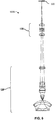
- Figs. 7(A) to 7(D) illustrate aspects of dark-field inspection systems that incorporate the inventive photocathode in accordance with other exemplary embodiments of the present invention.
- inspection system 300B-1 illuminates line 18 by light 14 that is passed through optics 11 comprising lens or mirror 12 onto the surface 20 of the wafer or photomask (sample) being inspected.
- Collection optics 21 direct scattered light from that line to sensor 200 using lenses and/or mirrors such as 22a and 22b.
- the optical axis 28 of the collection optics is not in the illumination plane of line 18. In some embodiments, axis 28 is approximately perpendicular to the line 18.
Landscapes
- Physics & Mathematics (AREA)
- Analytical Chemistry (AREA)
- General Physics & Mathematics (AREA)
- Chemical & Material Sciences (AREA)
- Immunology (AREA)
- General Health & Medical Sciences (AREA)
- Life Sciences & Earth Sciences (AREA)
- Health & Medical Sciences (AREA)
- Pathology (AREA)
- Optics & Photonics (AREA)
- Biochemistry (AREA)
- Common Detailed Techniques For Electron Tubes Or Discharge Tubes (AREA)
- Image-Pickup Tubes, Image-Amplification Tubes, And Storage Tubes (AREA)
- Photovoltaic Devices (AREA)
- Investigating Materials By The Use Of Optical Means Adapted For Particular Applications (AREA)
- Testing Or Measuring Of Semiconductors Or The Like (AREA)
- Exposure And Positioning Against Photoresist Photosensitive Materials (AREA)
- Preparing Plates And Mask In Photomechanical Process (AREA)
Claims (15)
- Photokathode (100), umfassend:ein Siliziumsubstrat (101), das sich gegenüberliegende erste und zweite Oberflächen (102; 103) aufweist;eine erste Schicht (104), die aus Boron besteht, das direkt an der zweiten Oberfläche (103) des Siliziumsubtrats angeordnet ist; undeine zweite Schicht (105), die ein Material mit niedriger Austrittsarbeit umfasst, das an der ersten Schicht (104) angeordnet ist.
- Photokathode (100) nach Anspruch 1, wobei das Material mit niedriger Austrittsarbeit eines von einem Alkalimetall und einem Alkalimetalloxid umfasst.
- Photokathode (100) nach Anspruch 2, wobei das Material mit niedriger Austrittsarbeit Cäsium umfasst.
- Photokathode (100) nach Anspruch 1, wobei die erste Schicht (104) eine Dicke im Bereich von ungefähr 1 nm bis 5 nm aufweist.
- Photokathode (100A) nach Anspruch 1, die ferner eine dritte Schicht (106) umfasst, die aus Boron besteht, das direkt an der ersten Oberfläche (102) des Siliziumsubstrats (101) angeordnet ist.
- Photokathode (100B) nach Anspruch 5, die ferner eine vierte Schicht (107) umfasst, die ein nicht reflektierendes Material umfasst, das an der dritten Schicht (106) angeordnet ist.
- Photokathode (100) nach Anspruch 4, die ferner Hilfsmittel zum Erzeugen eines Potenzialunterschieds zwischen der ersten und zweiten Oberfläche (102; 103) des Siliziumsubstrats (101) umfasst.
- Photokathode (100) nach Anspruch 1, wobei das Siliziumsubstrat (101) einen p-Diffussionsbereich beinhaltet, der sich von der ersten Oberfläche (102) in Richtung der zweiten Oberfläche (103) derartig erstreckt, dass der p-Diffusionsbereich eine höhere Konzentration des p-Dotierstoffes in Abschnitten nahe der ersten Oberfläche (102) aufweist als in Abschnitten, die entfernt der ersten Oberfläche (102) angeordnet sind.
- Sensor (200A; 200B; 200C) zum Erzeugen eines elektrischen Signals als Reaktion auf Photonen, die auf eine Aufnahmeoberfläche (203A) gerichtet sind, wobei der Sensor Folgendes umfasst:eine Photokathode (100) nach einem der Ansprüche 1 bis 8, die angrenzend an die Aufnahmeoberfläche (203A) zum Emittieren von Photoelektronen als Reaktion auf die Photonen angeordnet ist, wobei bei dem Siliziumsubstrat (101) der Photokathode (100) die erste Oberfläche (102) auf die Aufnahmeoberfläche (203A) gerichtet ist und die zweite Oberfläche (103) von der Aufnahmeoberfläche (203A) weg gerichtet ist,eine Erfassungsvorrichtung (210) die eine Erfassungsoberfläche (212) aufweist, die auf die zweite Oberfläche (105) gerichtet ist, wobei die Erfassungsvorrichtung (210) Hilfsmittel zum Erfassen der Photoelektronen, die durch die Photokathode (100) emittiert werden, und Hilfsmittel zum Erzeugen des elektrischen Signals als Reaktion auf die erfassten Photoelektronen beinhaltet;ein Gehäuse (202) das zwischen der Photokathode (100) und der Erfassungsvorrichtung (210) derartig wirkverbunden ist, dass die Erfassungsoberfläche (212) der Erfassungsvorrichtung (210) von der zweiten Schicht (105) der Photokathode (100) durch eine dazwischenliegendes Spaltgebiet (206) getrennt ist; undHilfsmittel zum derartigen Erzeugen eines elektrischen Feldes zwischen der Photokathode (100) und der Erfassungsvorrichtung (210), dass die Elektronen, die von der Photokathode (100) in das Spaltgebiet (206) emittiert werden, durch das elektrische Feld in Richtung der Erfassungsvorrichtung (210) beschleunigt werden.
- Sensor (200A; 200B; 200C) nach Anspruch 9, wobei der Sensor eine/n von einem Bildverstärker, einer mit Elektronen beschossenen ladungsgekoppelten Vorrichtung (EBCCD) und einem Photoverfielfacher umfasst.
- Sensor (200B) nach Anspruch 9, der die Fotokathode nach Anspruch 6 umfasst, wobei die Aufnahmeoberfläche des Sensors eine Außenfläche der vierten Schicht (107) umfasst.
- Sensor (200C) nach Anspruch 9, wobei die Aufnahmeoberfläche (203C) eine Schicht nicht reflektierenden Materials (207C) umfasst, die an einem Fenster (204C) angeordnet ist.
- Sensor (200B) nach Anspruch 9, wobei die Erfassungsvorrichtung (210) ein zweites Siliziumsubstrat (211C) umfasst und eine Boronschicht (106) beinhaltet, die direkt auf der Erfassungsoberfläche des Siliziumsubstrats (101) angeordnet ist.
- Kontrollsystem (300A, 300B1), umfassend:eine Lichtquelle zum Übermitteln von Photonen auf eine Probe;einen Sensor (200) zum Erfassen von Photonen von der Probe; undein optisches System zum Leiten der Photonen von der Lichtquelle auf die Probe und von der Probe zum Sensor,wobei der Sensor (200) Folgendes umfasst:eine Photokathode (100), die angrenzend an die Aufnahmeoberfläche zum Emittieren von Photoelektronen als Reaktion auf die Photonen angeordnet ist, wobei die Photokathode(100) Folgendes beinhaltet:ein monokristallines Siliziumsubstrat (101), das eine erste Oberfläche (102), die in Richtung des optischen Systems gerichtet ist, und eine zweite Oberfläche (103) aufweist, die vom optischen System weg gerichtet ist,eine erste Schicht (104) die aus Boron besteht, das direkt an der zweiten Oberfläche (103) des Siliziumsubstrats (101) angeordnet ist, undeine zweite Schicht (105), die ein Material mit niedriger Austrittsfunktion umfasst, das an der ersten Schicht (104) angeordnet ist;
undeine Erfassungsvorrichtung (210), die eine Erfassungsoberfläche (212) aufweist, die auf die zweite Schicht (105) gerichtet ist, wobei die Erfassungsvorrichtung (210) Hilfsmittel zum Erfassen der Photoelektronen, die durch die Photokathode (100) emittiert werden, und Hilfsmittel zum Erzeugen des elektrischen Signals als Reaktion auf die erfassten Photoelektronen beinhaltet. - Kontrollsystem (300A, 300B1) nach Anspruch 14, wobei der Sensor (200) eine/n von einem Bildverstärker, einer mit Elektronen beschossenen ladungsgekoppelten Vorrichtung (EBCCD) und einem Photovervielfacher umfasst.
Applications Claiming Priority (3)
| Application Number | Priority Date | Filing Date | Title |
|---|---|---|---|
| US201261679200P | 2012-08-03 | 2012-08-03 | |
| US13/947,975 US9601299B2 (en) | 2012-08-03 | 2013-07-22 | Photocathode including silicon substrate with boron layer |
| PCT/US2013/052546 WO2014022297A1 (en) | 2012-08-03 | 2013-07-29 | Photocathode including silicon substrate with boron layer |
Publications (3)
| Publication Number | Publication Date |
|---|---|
| EP2880693A1 EP2880693A1 (de) | 2015-06-10 |
| EP2880693A4 EP2880693A4 (de) | 2016-06-01 |
| EP2880693B1 true EP2880693B1 (de) | 2018-01-03 |
Family
ID=50024546
Family Applications (1)
| Application Number | Title | Priority Date | Filing Date |
|---|---|---|---|
| EP13825872.8A Active EP2880693B1 (de) | 2012-08-03 | 2013-07-29 | Photokathode mit einem siliciumsubstrat mit einer borschicht |
Country Status (7)
| Country | Link |
|---|---|
| US (3) | US9601299B2 (de) |
| EP (1) | EP2880693B1 (de) |
| JP (3) | JP6257622B2 (de) |
| KR (3) | KR102304825B1 (de) |
| CN (2) | CN108155200B (de) |
| TW (1) | TWI635602B (de) |
| WO (1) | WO2014022297A1 (de) |
Families Citing this family (51)
| Publication number | Priority date | Publication date | Assignee | Title |
|---|---|---|---|---|
| US9793673B2 (en) | 2011-06-13 | 2017-10-17 | Kla-Tencor Corporation | Semiconductor inspection and metrology system using laser pulse multiplier |
| US10197501B2 (en) | 2011-12-12 | 2019-02-05 | Kla-Tencor Corporation | Electron-bombarded charge-coupled device and inspection systems using EBCCD detectors |
| US9496425B2 (en) | 2012-04-10 | 2016-11-15 | Kla-Tencor Corporation | Back-illuminated sensor with boron layer |
| US9601299B2 (en) | 2012-08-03 | 2017-03-21 | Kla-Tencor Corporation | Photocathode including silicon substrate with boron layer |
| NL2011568A (en) * | 2012-10-31 | 2014-05-06 | Asml Netherlands Bv | Sensor and lithographic apparatus. |
| US9151940B2 (en) | 2012-12-05 | 2015-10-06 | Kla-Tencor Corporation | Semiconductor inspection and metrology system using laser pulse multiplier |
| US9529182B2 (en) | 2013-02-13 | 2016-12-27 | KLA—Tencor Corporation | 193nm laser and inspection system |
| US9608399B2 (en) | 2013-03-18 | 2017-03-28 | Kla-Tencor Corporation | 193 nm laser and an inspection system using a 193 nm laser |
| US9478402B2 (en) | 2013-04-01 | 2016-10-25 | Kla-Tencor Corporation | Photomultiplier tube, image sensor, and an inspection system using a PMT or image sensor |
| US9347890B2 (en) | 2013-12-19 | 2016-05-24 | Kla-Tencor Corporation | Low-noise sensor and an inspection system using a low-noise sensor |
| US9748294B2 (en) | 2014-01-10 | 2017-08-29 | Hamamatsu Photonics K.K. | Anti-reflection layer for back-illuminated sensor |
| US9202837B2 (en) | 2014-01-22 | 2015-12-01 | Taiwan Semiconductor Manufacturing Co., Ltd. | Image-sensor device and method of manufacturing the same |
| US9410901B2 (en) | 2014-03-17 | 2016-08-09 | Kla-Tencor Corporation | Image sensor, an inspection system and a method of inspecting an article |
| US9804101B2 (en) | 2014-03-20 | 2017-10-31 | Kla-Tencor Corporation | System and method for reducing the bandwidth of a laser and an inspection system and method using a laser |
| CN105306613A (zh) * | 2014-07-24 | 2016-02-03 | 中兴通讯股份有限公司 | Esadi的mac地址通告方法、装置及获取装置 |
| US9767986B2 (en) | 2014-08-29 | 2017-09-19 | Kla-Tencor Corporation | Scanning electron microscope and methods of inspecting and reviewing samples |
| US9748729B2 (en) | 2014-10-03 | 2017-08-29 | Kla-Tencor Corporation | 183NM laser and inspection system |
| CZ306489B6 (cs) * | 2014-11-03 | 2017-02-08 | Crytur, Spol.S R.O. | Zařízení pro koincidenční zobrazování sekundárními elektrony |
| US10748730B2 (en) * | 2015-05-21 | 2020-08-18 | Kla-Tencor Corporation | Photocathode including field emitter array on a silicon substrate with boron layer |
| US10133181B2 (en) * | 2015-08-14 | 2018-11-20 | Kla-Tencor Corporation | Electron source |
| US10462391B2 (en) | 2015-08-14 | 2019-10-29 | Kla-Tencor Corporation | Dark-field inspection using a low-noise sensor |
| US10778925B2 (en) | 2016-04-06 | 2020-09-15 | Kla-Tencor Corporation | Multiple column per channel CCD sensor architecture for inspection and metrology |
| US10313622B2 (en) | 2016-04-06 | 2019-06-04 | Kla-Tencor Corporation | Dual-column-parallel CCD sensor and inspection systems using a sensor |
| CN109661611B (zh) * | 2016-10-10 | 2021-12-21 | 金泰克斯公司 | 偏振窗组合件 |
| US9966230B1 (en) * | 2016-10-13 | 2018-05-08 | Kla-Tencor Corporation | Multi-column electron beam lithography including field emitters on a silicon substrate with boron layer |
| US10175555B2 (en) | 2017-01-03 | 2019-01-08 | KLA—Tencor Corporation | 183 nm CW laser and inspection system |
| WO2018222528A1 (en) | 2017-05-30 | 2018-12-06 | Carrier Corporation | Semiconductor film and phototube light detector |
| US10692683B2 (en) * | 2017-09-12 | 2020-06-23 | Intevac, Inc. | Thermally assisted negative electron affinity photocathode |
| US10535493B2 (en) | 2017-10-10 | 2020-01-14 | Kla-Tencor Corporation | Photocathode designs and methods of generating an electron beam using a photocathode |
| US10395884B2 (en) * | 2017-10-10 | 2019-08-27 | Kla-Tencor Corporation | Ruthenium encapsulated photocathode electron emitter |
| CN108231507B (zh) * | 2017-12-12 | 2020-06-23 | 东南大学 | 一种基于新型纳米结构的光阴极及其制备方法 |
| CN110574172B (zh) * | 2018-03-30 | 2023-02-28 | 国立大学法人茨城大学 | 光电二极管以及光感应设备 |
| US11114489B2 (en) | 2018-06-18 | 2021-09-07 | Kla-Tencor Corporation | Back-illuminated sensor and a method of manufacturing a sensor |
| US10714295B2 (en) * | 2018-09-18 | 2020-07-14 | Kla-Tencor Corporation | Metal encapsulated photocathode electron emitter |
| US10943760B2 (en) | 2018-10-12 | 2021-03-09 | Kla Corporation | Electron gun and electron microscope |
| US11629551B2 (en) | 2018-10-21 | 2023-04-18 | Gentex Corporation | Electro-optic window assembly |
| US11114491B2 (en) | 2018-12-12 | 2021-09-07 | Kla Corporation | Back-illuminated sensor and a method of manufacturing a sensor |
| DE202020005866U1 (de) | 2019-01-07 | 2022-12-05 | Gentex Corporation | Fensteranordnung mit variabler Transmission |
| FR3096506B1 (fr) * | 2019-05-23 | 2021-06-11 | Photonis France | Photocathode à rendement quantique amélioré |
| US11417492B2 (en) | 2019-09-26 | 2022-08-16 | Kla Corporation | Light modulated electron source |
| US12613197B2 (en) * | 2019-12-03 | 2026-04-28 | Kla Corporation | Low-reflectivity back-illuminated image sensor |
| CN111261488B (zh) * | 2020-01-29 | 2022-04-22 | 北方夜视技术股份有限公司 | 光电倍增管玻璃光窗的金属氮化物增透膜、制备方法、制备系统及光电倍增管 |
| US11201041B2 (en) * | 2020-02-03 | 2021-12-14 | Baker Hughes Holdings Llc | Gas electron multiplier board photomultiplier |
| US11668601B2 (en) * | 2020-02-24 | 2023-06-06 | Kla Corporation | Instrumented substrate apparatus |
| US11848350B2 (en) | 2020-04-08 | 2023-12-19 | Kla Corporation | Back-illuminated sensor and a method of manufacturing a sensor using a silicon on insulator wafer |
| US12119199B2 (en) * | 2020-04-13 | 2024-10-15 | Institute Of Microelectronics Of The Chinese Academy Of Sciences | Power device and fabrication method thereof |
| EP3913356B1 (de) * | 2020-05-18 | 2025-01-22 | Imec VZW | Verfahren zur messung der fallendichte in einem 2-dimensionalen halbleitermaterial |
| CN112885683B (zh) * | 2021-01-14 | 2022-06-10 | 北方夜视技术股份有限公司 | 镀制SiO2或Al2O3材质的介质膜的锑碱光电阴极及镀制方法 |
| CN113241293B (zh) * | 2021-04-30 | 2022-03-18 | 中建材光子科技有限公司 | 具有超高阴极灵敏度的防光晕玻璃组件及其制备方法和应用 |
| US12523354B2 (en) | 2021-11-26 | 2026-01-13 | Biolight Corp. | Ultra-microlight transmission device using secondary electrons |
| US12484316B2 (en) | 2024-02-29 | 2025-11-25 | Kla Corporation | CVD boron uniformity overcoming loading effects |
Family Cites Families (194)
| Publication number | Priority date | Publication date | Assignee | Title |
|---|---|---|---|---|
| US3755704A (en) | 1970-02-06 | 1973-08-28 | Stanford Research Inst | Field emission cathode structures and devices utilizing such structures |
| US3870917A (en) | 1971-05-10 | 1975-03-11 | Itt | Discharge device including channel type electron multiplier having ion adsorptive layer |
| GB1444951A (en) * | 1973-06-18 | 1976-08-04 | Mullard Ltd | Electronic solid state devices |
| GB1536412A (en) | 1975-05-14 | 1978-12-20 | English Electric Valve Co Ltd | Photocathodes |
| US4210922A (en) | 1975-11-28 | 1980-07-01 | U.S. Philips Corporation | Charge coupled imaging device having selective wavelength sensitivity |
| NL7611593A (nl) * | 1976-10-20 | 1978-04-24 | Optische Ind De Oude Delft Nv | Werkwijze voor het in een beeldversterkerbuis aanbrengen van een lichtabsorberende, voor elek- tronen doorlaatbare laag. |
| JPS58146B2 (ja) | 1980-10-14 | 1983-01-05 | 浜松テレビ株式会社 | フレ−ミング管 |
| US4348690A (en) | 1981-04-30 | 1982-09-07 | Rca Corporation | Semiconductor imagers |
| US4644221A (en) | 1981-05-06 | 1987-02-17 | The United States Of America As Represented By The Secretary Of The Army | Variable sensitivity transmission mode negative electron affinity photocathode |
| JPS60180052A (ja) * | 1984-02-24 | 1985-09-13 | Hamamatsu Photonics Kk | 光電子または2次電子放射用陰極 |
| US4555731A (en) | 1984-04-30 | 1985-11-26 | Polaroid Corporation | Electronic imaging camera with microchannel plate |
| US4760031A (en) | 1986-03-03 | 1988-07-26 | California Institute Of Technology | Producing CCD imaging sensor with flashed backside metal film |
| US4853595A (en) | 1987-08-31 | 1989-08-01 | Alfano Robert R | Photomultiplier tube having a transmission strip line photocathode and system for use therewith |
| NL8902271A (nl) | 1989-09-12 | 1991-04-02 | Philips Nv | Werkwijze voor het verbinden van twee lichamen. |
| US5120949A (en) | 1991-01-17 | 1992-06-09 | Burle Technologies, Inc. | Semiconductor anode photomultiplier tube |
| JP2828221B2 (ja) | 1991-06-04 | 1998-11-25 | インターナショナル・ビジネス・マシーンズ・コーポレイション | レーザー光波長変換装置 |
| JPH0512989A (ja) * | 1991-07-01 | 1993-01-22 | Nec Corp | 半導体光電面およびその製造方法 |
| US5563702A (en) | 1991-08-22 | 1996-10-08 | Kla Instruments Corporation | Automated photomask inspection apparatus and method |
| US5268570A (en) * | 1991-12-20 | 1993-12-07 | Litton Systems, Inc. | Transmission mode InGaAs photocathode for night vision system |
| US5376810A (en) | 1992-06-26 | 1994-12-27 | California Institute Of Technology | Growth of delta-doped layers on silicon CCD/S for enhanced ultraviolet response |
| US5227313A (en) | 1992-07-24 | 1993-07-13 | Eastman Kodak Company | Process for making backside illuminated image sensors |
| US5315126A (en) | 1992-10-13 | 1994-05-24 | Itt Corporation | Highly doped surface layer for negative electron affinity devices |
| US5326978A (en) | 1992-12-17 | 1994-07-05 | Intevac, Inc. | Focused electron-bombarded detector |
| US5475227A (en) | 1992-12-17 | 1995-12-12 | Intevac, Inc. | Hybrid photomultiplier tube with ion deflector |
| US5760809A (en) | 1993-03-19 | 1998-06-02 | Xerox Corporation | Recording sheets containing phosphonium compounds |
| FI940740A0 (fi) | 1994-02-17 | 1994-02-17 | Arto Salokatve | Detektor foer paovisning av fotoner eller partiklar, foerfarande foer framstaellning av detektorn och maetningsfoerfarande |
| US6271916B1 (en) | 1994-03-24 | 2001-08-07 | Kla-Tencor Corporation | Process and assembly for non-destructive surface inspections |
| US5493176A (en) | 1994-05-23 | 1996-02-20 | Siemens Medical Systems, Inc. | Photomultiplier tube with an avalanche photodiode, a flat input end and conductors which simulate the potential distribution in a photomultiplier tube having a spherical-type input end |
| US20080315092A1 (en) | 1994-07-28 | 2008-12-25 | General Nanotechnology Llc | Scanning probe microscopy inspection and modification system |
| EP0702221A3 (de) | 1994-09-14 | 1997-05-21 | Delco Electronics Corp | Auf einem Chip integrierter Sensor |
| JPH08241977A (ja) | 1995-03-03 | 1996-09-17 | Hamamatsu Photonics Kk | 半導体装置の製造方法 |
| ATE313857T1 (de) | 1995-05-19 | 2006-01-15 | Heidenhain Gmbh Dr Johannes | Strahlungsempfindliches detektorelement |
| US5731584A (en) | 1995-07-14 | 1998-03-24 | Imec Vzw | Position sensitive particle sensor and manufacturing method therefor |
| US6362484B1 (en) | 1995-07-14 | 2002-03-26 | Imec Vzw | Imager or particle or radiation detector and method of manufacturing the same |
| EP0979398B1 (de) | 1996-06-04 | 2012-01-04 | KLA-Tencor Corporation | Optische rastervorrichtung fur oberflaechenpruefung |
| US5999310A (en) | 1996-07-22 | 1999-12-07 | Shafer; David Ross | Ultra-broadband UV microscope imaging system with wide range zoom capability |
| US5717518A (en) | 1996-07-22 | 1998-02-10 | Kla Instruments Corporation | Broad spectrum ultraviolet catadioptric imaging system |
| US5742626A (en) | 1996-08-14 | 1998-04-21 | Aculight Corporation | Ultraviolet solid state laser, method of using same and laser surgery apparatus |
| US5760899A (en) | 1996-09-04 | 1998-06-02 | Erim International, Inc. | High-sensitivity multispectral sensor |
| US6201257B1 (en) | 1996-10-10 | 2001-03-13 | Advanced Scientific Concepts, Inc. | Semiconductor X-ray photocathodes devices |
| US5940685A (en) | 1996-10-28 | 1999-08-17 | The United States Of America As Represented By The Secretary Of The Air Force | Fabrication of UV-sensitive back illuminated CCD image sensors |
| US6064759A (en) | 1996-11-08 | 2000-05-16 | Buckley; B. Shawn | Computer aided inspection machine |
| JPH10171965A (ja) | 1996-12-05 | 1998-06-26 | Toshiba Corp | 積算型エリアセンサの画像入力方法及びその装置 |
| US6107619A (en) | 1997-07-14 | 2000-08-22 | California Institute Of Technology | Delta-doped hybrid advanced detector for low energy particle detection |
| US6608676B1 (en) | 1997-08-01 | 2003-08-19 | Kla-Tencor Corporation | System for detecting anomalies and/or features of a surface |
| US6201601B1 (en) | 1997-09-19 | 2001-03-13 | Kla-Tencor Corporation | Sample inspection system |
| US6403963B1 (en) | 1997-09-29 | 2002-06-11 | California Institute Of Technology | Delta-doped CCD's as low-energy particle detectors and imagers |
| US6278119B1 (en) | 1997-10-21 | 2001-08-21 | California Institute Of Technology | Using a delta-doped CCD to determine the energy of a low-energy particle |
| US6297879B1 (en) | 1998-02-27 | 2001-10-02 | Micron Technology, Inc. | Inspection method and apparatus for detecting defects on photomasks |
| US6376985B2 (en) | 1998-03-31 | 2002-04-23 | Applied Materials, Inc. | Gated photocathode for controlled single and multiple electron beam emission |
| US6162707A (en) * | 1998-05-18 | 2000-12-19 | The Regents Of The University Of California | Low work function, stable thin films |
| JP3806514B2 (ja) * | 1998-06-22 | 2006-08-09 | 浜松ホトニクス株式会社 | 光電面及びその製造方法 |
| US6373869B1 (en) | 1998-07-30 | 2002-04-16 | Actinix | System and method for generating coherent radiation at ultraviolet wavelengths |
| JP4229500B2 (ja) * | 1998-11-09 | 2009-02-25 | 株式会社神戸製鋼所 | 反射型光電陰極 |
| US6013399A (en) | 1998-12-04 | 2000-01-11 | Advanced Micro Devices, Inc. | Reworkable EUV mask materials |
| US6535531B1 (en) | 2001-11-29 | 2003-03-18 | Cymer, Inc. | Gas discharge laser with pulse multiplier |
| US6657178B2 (en) | 1999-07-20 | 2003-12-02 | Intevac, Inc. | Electron bombarded passive pixel sensor imaging |
| US6307586B1 (en) | 1999-07-20 | 2001-10-23 | Intevac, Inc. | Electron bombarded active pixel sensor camera incorporating gain control |
| US6285018B1 (en) | 1999-07-20 | 2001-09-04 | Intevac, Inc. | Electron bombarded active pixel sensor |
| US6549647B1 (en) | 2000-01-07 | 2003-04-15 | Cyberoptics Corporation | Inspection system with vibration resistant video capture |
| US6711283B1 (en) | 2000-05-03 | 2004-03-23 | Aperio Technologies, Inc. | Fully automatic rapid microscope slide scanner |
| JP2002033473A (ja) | 2000-07-17 | 2002-01-31 | Hamamatsu Photonics Kk | 半導体装置 |
| US6879390B1 (en) | 2000-08-10 | 2005-04-12 | Kla-Tencor Technologies Corporation | Multiple beam inspection apparatus and method |
| US6507147B1 (en) | 2000-08-31 | 2003-01-14 | Intevac, Inc. | Unitary vacuum tube incorporating high voltage isolation |
| JP2002184302A (ja) | 2000-12-18 | 2002-06-28 | Hamamatsu Photonics Kk | 半導体光電陰極 |
| US6704339B2 (en) | 2001-01-29 | 2004-03-09 | Cymer, Inc. | Lithography laser with beam delivery and beam pointing control |
| US6545281B1 (en) | 2001-07-06 | 2003-04-08 | The United States Of America As Represented By The United States Department Of Energy | Pocked surface neutron detector |
| JP3573725B2 (ja) | 2001-08-03 | 2004-10-06 | 川崎重工業株式会社 | X線顕微鏡装置 |
| JP2003043533A (ja) | 2001-08-03 | 2003-02-13 | Kitakyushu Foundation For The Advancement Of Industry Science & Technology | レーザーの第二高調波の方向を一定に保つための自動追尾装置 |
| US6747258B2 (en) | 2001-10-09 | 2004-06-08 | Itt Manufacturing Enterprises, Inc. | Intensified hybrid solid-state sensor with an insulating layer |
| US7015452B2 (en) | 2001-10-09 | 2006-03-21 | Itt Manufacturing Enterprises, Inc. | Intensified hybrid solid-state sensor |
| WO2003043045A2 (en) * | 2001-11-13 | 2003-05-22 | Nanosciences Corporation | Photocathode |
| US7130039B2 (en) | 2002-04-18 | 2006-10-31 | Kla-Tencor Technologies Corporation | Simultaneous multi-spot inspection and imaging |
| JP4165129B2 (ja) | 2002-06-21 | 2008-10-15 | 三菱電機株式会社 | 裏面入射型固体撮像素子 |
| US20040021061A1 (en) | 2002-07-30 | 2004-02-05 | Frederik Bijkerk | Photodiode, charged-coupled device and method for the production |
| US7446474B2 (en) | 2002-10-10 | 2008-11-04 | Applied Materials, Inc. | Hetero-junction electron emitter with Group III nitride and activated alkali halide |
| US7283166B1 (en) | 2002-10-15 | 2007-10-16 | Lockheed Martin Corporation | Automatic control method and system for electron bombarded charge coupled device (“EBCCD”) sensor |
| US7126699B1 (en) | 2002-10-18 | 2006-10-24 | Kla-Tencor Technologies Corp. | Systems and methods for multi-dimensional metrology and/or inspection of a specimen |
| US7005637B2 (en) | 2003-01-31 | 2006-02-28 | Intevac, Inc. | Backside thinning of image array devices |
| US6990385B1 (en) | 2003-02-03 | 2006-01-24 | Kla-Tencor Technologies Corporation | Defect detection using multiple sensors and parallel processing |
| GB2398118B (en) * | 2003-02-07 | 2006-03-15 | Imp College Innovations Ltd | Photon arrival time detection |
| US7141785B2 (en) | 2003-02-13 | 2006-11-28 | Micromass Uk Limited | Ion detector |
| US7957066B2 (en) | 2003-02-21 | 2011-06-07 | Kla-Tencor Corporation | Split field inspection system using small catadioptric objectives |
| US7813406B1 (en) | 2003-10-15 | 2010-10-12 | The United States Of America As Represented By The Administrator Of The National Aeronautics And Space Administration | Temporal laser pulse manipulation using multiple optical ring-cavities |
| US7023126B2 (en) | 2003-12-03 | 2006-04-04 | Itt Manufacturing Enterprises Inc. | Surface structures for halo reduction in electron bombarded devices |
| US7321468B2 (en) | 2003-12-15 | 2008-01-22 | Carl Zeiss Laser Optics Gmbh | Method and optical arrangement for beam guiding of a light beam with beam delay |
| US7313155B1 (en) | 2004-02-12 | 2007-12-25 | Liyue Mu | High power Q-switched laser for soft tissue ablation |
| US7035012B2 (en) | 2004-03-01 | 2006-04-25 | Coherent, Inc. | Optical pulse duration extender |
| JP4365255B2 (ja) | 2004-04-08 | 2009-11-18 | 浜松ホトニクス株式会社 | 発光体と、これを用いた電子線検出器、走査型電子顕微鏡及び質量分析装置 |
| US7301263B2 (en) | 2004-05-28 | 2007-11-27 | Applied Materials, Inc. | Multiple electron beam system with electron transmission gates |
| KR100688497B1 (ko) | 2004-06-28 | 2007-03-02 | 삼성전자주식회사 | 이미지 센서 및 그 제조방법 |
| JP4500641B2 (ja) | 2004-09-29 | 2010-07-14 | 株式会社日立ハイテクノロジーズ | 欠陥検査方法およびその装置 |
| US7455565B2 (en) | 2004-10-13 | 2008-11-25 | The Board Of Trustees Of The Leland Stanford Junior University | Fabrication of group III-nitride photocathode having Cs activation layer |
| US7609309B2 (en) | 2004-11-18 | 2009-10-27 | Kla-Tencor Technologies Corporation | Continuous clocking of TDI sensors |
| US7952633B2 (en) | 2004-11-18 | 2011-05-31 | Kla-Tencor Technologies Corporation | Apparatus for continuous clocking of TDI sensors |
| US7432517B2 (en) | 2004-11-19 | 2008-10-07 | Asml Netherlands B.V. | Pulse modifier, lithographic apparatus, and device manufacturing method |
| JP4751617B2 (ja) | 2005-01-21 | 2011-08-17 | 株式会社日立ハイテクノロジーズ | 欠陥検査方法及びその装置 |
| DE602006004913D1 (de) | 2005-04-28 | 2009-03-12 | Semiconductor Energy Lab | Verfahren und Vorrichtung zur Herstellung von Halbleitern mittels Laserstrahlung |
| US7531826B2 (en) | 2005-06-01 | 2009-05-12 | Intevac, Inc. | Photocathode structure and operation |
| EP1734584A1 (de) | 2005-06-14 | 2006-12-20 | Photonis-DEP B.V. | Elektronenbeschossene Bildsensorvorrichtung, sowie eine solche Bildsensoranordnung |
| US7345825B2 (en) | 2005-06-30 | 2008-03-18 | Kla-Tencor Technologies Corporation | Beam delivery system for laser dark-field illumination in a catadioptric optical system |
| JP4491391B2 (ja) | 2005-08-05 | 2010-06-30 | 株式会社日立ハイテクノロジーズ | 欠陥検査装置及び欠陥検査方法 |
| JP5403852B2 (ja) | 2005-08-12 | 2014-01-29 | 株式会社荏原製作所 | 検出装置及び検査装置 |
| CN101263201B (zh) | 2005-09-16 | 2012-10-17 | 松下电器产业株式会社 | 复合材料、及使用该材料的光学部件 |
| US7532145B2 (en) | 2005-09-21 | 2009-05-12 | Rjs Technologies Inc. | High resolution and wide dynamic range integrator |
| JP4939033B2 (ja) | 2005-10-31 | 2012-05-23 | 浜松ホトニクス株式会社 | 光電陰極 |
| US7715459B2 (en) | 2005-11-01 | 2010-05-11 | Cymer, Inc. | Laser system |
| JP2007133102A (ja) | 2005-11-09 | 2007-05-31 | Canon Inc | 反射防止膜を有する光学素子及びそれを有する露光装置 |
| US7528943B2 (en) | 2005-12-27 | 2009-05-05 | Kla-Tencor Technologies Corporation | Method and apparatus for simultaneous high-speed acquisition of multiple images |
| JP4911494B2 (ja) | 2006-03-18 | 2012-04-04 | 国立大学法人大阪大学 | 波長変換光学素子、波長変換光学素子の製造方法、波長変換装置、紫外線レーザ照射装置およびレーザ加工装置 |
| JP4706850B2 (ja) | 2006-03-23 | 2011-06-22 | 富士フイルム株式会社 | ノズルプレートの製造方法、液滴吐出ヘッド及び画像形成装置 |
| WO2007112058A2 (en) | 2006-03-24 | 2007-10-04 | Applied Materials, Inc. | Carbon precursors for use during silicon epitaxial firm formation |
| US7113325B1 (en) | 2006-05-03 | 2006-09-26 | Mitsubishi Materials Corporation | Wavelength conversion method with improved conversion efficiency |
| US8472111B2 (en) | 2006-06-13 | 2013-06-25 | The Arizona Board Of Regents On Behalf Of The University Of Arizona | Apparatus and method for deep ultraviolet optical microscopy |
| US7457330B2 (en) | 2006-06-15 | 2008-11-25 | Pavilion Integration Corporation | Low speckle noise monolithic microchip RGB lasers |
| US8482197B2 (en) | 2006-07-05 | 2013-07-09 | Hamamatsu Photonics K.K. | Photocathode, electron tube, field assist type photocathode, field assist type photocathode array, and field assist type electron tube |
| US7791170B2 (en) | 2006-07-10 | 2010-09-07 | Taiwan Semiconductor Manufacturing Company, Ltd. | Method of making a deep junction for electrical crosstalk reduction of an image sensor |
| TWI312558B (en) | 2006-08-21 | 2009-07-21 | Ase Shanghai Inc | Packaging substrate board and method of manufacturing the same |
| US7800040B2 (en) | 2006-09-21 | 2010-09-21 | California Institute Of Technology | Method for growing a back surface contact on an imaging detector used in conjunction with back illumination |
| KR100826407B1 (ko) | 2006-10-12 | 2008-05-02 | 삼성전기주식회사 | 자외선 수광용 포토 다이오드 및 이를 포함하는 이미지센서 |
| KR100874954B1 (ko) | 2006-12-04 | 2008-12-19 | 삼성전자주식회사 | 후면 수광 이미지 센서 |
| JP5342769B2 (ja) | 2006-12-28 | 2013-11-13 | 浜松ホトニクス株式会社 | 光電陰極、電子管及び光電子増倍管 |
| US20080173903A1 (en) | 2006-12-28 | 2008-07-24 | Fujifilm Corporation | Solid-state image pickup element |
| US9771666B2 (en) | 2007-01-17 | 2017-09-26 | Crystal Is, Inc. | Defect reduction in seeded aluminum nitride crystal growth |
| WO2008088838A1 (en) | 2007-01-17 | 2008-07-24 | Crystal Is, Inc. | Defect reduction in seeded aluminum nitride crystal growth |
| US20110073982A1 (en) | 2007-05-25 | 2011-03-31 | Armstrong J Joseph | Inspection system using back side illuminated linear sensor |
| JP2008306080A (ja) * | 2007-06-11 | 2008-12-18 | Hitachi Ltd | 光センサ素子、およびこれを用いた光センサ装置、画像表示装置 |
| US8138485B2 (en) | 2007-06-25 | 2012-03-20 | Asml Netherlands B.V. | Radiation detector, method of manufacturing a radiation detector, and lithographic apparatus comprising a radiation detector |
| US7586108B2 (en) * | 2007-06-25 | 2009-09-08 | Asml Netherlands B.V. | Radiation detector, method of manufacturing a radiation detector and lithographic apparatus comprising a radiation detector |
| WO2009009081A2 (en) | 2007-07-10 | 2009-01-15 | Massachusetts Institute Of Technology | Tomographic phase microscopy |
| WO2009012222A1 (en) | 2007-07-13 | 2009-01-22 | Purdue Research Foundation | Time-resolved raman spectroscopy |
| US7999342B2 (en) | 2007-09-24 | 2011-08-16 | Taiwan Semiconductor Manufacturing Company, Ltd | Image sensor element for backside-illuminated sensor |
| JP5039495B2 (ja) | 2007-10-04 | 2012-10-03 | ルネサスエレクトロニクス株式会社 | マスクブランク検査方法、反射型露光マスクの製造方法、反射型露光方法および半導体集積回路の製造方法 |
| US7525649B1 (en) | 2007-10-19 | 2009-04-28 | Kla-Tencor Technologies Corporation | Surface inspection system using laser line illumination with two dimensional imaging |
| US7605376B2 (en) | 2007-10-29 | 2009-10-20 | Fairchild Imaging, Inc. | CMOS sensor adapted for dental x-ray imaging |
| JP5132262B2 (ja) | 2007-11-02 | 2013-01-30 | 三菱電機株式会社 | 裏面入射型リニアイメージセンサ、その駆動方法、及びその製造方法 |
| US7741666B2 (en) | 2008-02-08 | 2010-06-22 | Omnivision Technologies, Inc. | Backside illuminated imaging sensor with backside P+ doped layer |
| US8803075B2 (en) * | 2008-04-18 | 2014-08-12 | Saint-Gobain Ceramics & Plastics, Inc. | Radiation detector device |
| JP2010003755A (ja) | 2008-06-18 | 2010-01-07 | Mitsubishi Electric Corp | 波長変換レーザ装置 |
| JP5305377B2 (ja) | 2008-06-26 | 2013-10-02 | 株式会社フジクラ | ラマン光増幅を用いた光伝送システム |
| US20120170021A1 (en) | 2008-09-02 | 2012-07-05 | Phillip Walsh | Method and apparatus for providing multiple wavelength reflectance magnitude and phase for a sample |
| US7875948B2 (en) | 2008-10-21 | 2011-01-25 | Jaroslav Hynecek | Backside illuminated image sensor |
| US7880127B2 (en) | 2008-10-27 | 2011-02-01 | Itt Manufacturing Enterprises, Inc. | Apparatus and method for aligning an image sensor including a header alignment means |
| US8017427B2 (en) | 2008-12-31 | 2011-09-13 | Omnivision Technologies, Inc. | Backside-illuminated (BSI) image sensor with backside diffusion doping |
| US8581228B2 (en) | 2009-01-22 | 2013-11-12 | Bae Systems Information And Electronic Systems Integration Inc. | Corner cube enhanced photocathode |
| KR20100103238A (ko) | 2009-03-13 | 2010-09-27 | 삼성전자주식회사 | 에피 웨이퍼 제조 방법 및 그에 의해 제조된 에피 웨이퍼, 및 상기 에피 웨이퍼로 제조한 이미지 센서 |
| US20100301437A1 (en) | 2009-06-01 | 2010-12-02 | Kla-Tencor Corporation | Anti-Reflective Coating For Sensors Suitable For High Throughput Inspection Systems |
| US7985658B2 (en) | 2009-06-08 | 2011-07-26 | Aptina Imaging Corporation | Method of forming substrate for use in imager devices |
| WO2010148293A2 (en) | 2009-06-19 | 2010-12-23 | Kla-Tencor Corporation | Euv high throughput inspection system for defect detection on patterned euv masks, mask blanks, and wafers |
| KR20120039659A (ko) | 2009-06-22 | 2012-04-25 | 에이에스엠엘 홀딩 엔.브이. | 물체 검사 시스템 및 물체 검사 방법 |
| CN102035085B (zh) | 2009-10-08 | 2014-03-05 | 群康科技(深圳)有限公司 | 导电结构及其制造方法 |
| US8629384B1 (en) | 2009-10-26 | 2014-01-14 | Kla-Tencor Corporation | Photomultiplier tube optimized for surface inspection in the ultraviolet |
| US8598533B2 (en) | 2009-12-15 | 2013-12-03 | Saint-Gobain Ceramics & Plastics, Inc. | Radiation detection system and method of analyzing an electrical pulse output by a radiation detector |
| EP2346094A1 (de) * | 2010-01-13 | 2011-07-20 | FEI Company | Verfahren zur Herstellung eines Strahlungsdetektors |
| EP2526566B1 (de) | 2010-01-21 | 2018-03-07 | Roper Scientific, Inc. | Rückbeleuchteter festkörper-photonensensor und herstellungsverfahren dafür |
| PT3241840T (pt) | 2010-01-22 | 2022-10-13 | Univ Leland Stanford Junior | Inibição da sinalização de axl em terapêutica anti-metastática |
| US8558234B2 (en) | 2010-02-11 | 2013-10-15 | California Institute Of Technology | Low voltage low light imager and photodetector |
| CN102859338A (zh) | 2010-03-29 | 2013-01-02 | 因特瓦克公司 | 时间分辨光致发光成像系统和光伏电池检验的方法 |
| US8269223B2 (en) | 2010-05-27 | 2012-09-18 | The United States Of America As Represented By The Secretary Of The Army | Polarization enhanced avalanche photodetector and method thereof |
| US8310021B2 (en) | 2010-07-13 | 2012-11-13 | Honeywell International Inc. | Neutron detector with wafer-to-wafer bonding |
| WO2012021311A2 (en) | 2010-08-08 | 2012-02-16 | Kla-Tencor Corporation | Dynamic wavefront control of a frequency converted laser system |
| EP2652776B1 (de) | 2010-12-16 | 2019-08-07 | KLA-Tencor Corporation | Waferinspektion |
| US8669512B2 (en) | 2010-12-28 | 2014-03-11 | Technion Research & Development Foundation Limited | System and method for analyzing light by three-photon counting |
| US8513587B2 (en) | 2011-01-24 | 2013-08-20 | Taiwan Semiconductor Manufacturing Company, Ltd. | Image sensor with anti-reflection layer and method of manufacturing the same |
| US8455971B2 (en) | 2011-02-14 | 2013-06-04 | Taiwan Semiconductor Manufacturing Company, Ltd. | Apparatus and method for improving charge transfer in backside illuminated image sensor |
| JP2012189385A (ja) | 2011-03-09 | 2012-10-04 | Fujifilm Corp | 放射線画像検出装置の保守方法 |
| US9318870B2 (en) | 2011-05-06 | 2016-04-19 | Kla-Tencor Corporation | Deep ultra-violet light sources for wafer and reticle inspection systems |
| WO2013006867A1 (en) | 2011-07-07 | 2013-01-10 | Massachussetts Institute Of Technology | Methods and apparatus for ultrathin catalyst layer for photoelectrode |
| JP5731444B2 (ja) | 2011-07-07 | 2015-06-10 | 富士フイルム株式会社 | 放射線検出器、放射線画像撮影装置、及び放射線画像撮影システム |
| US9279774B2 (en) | 2011-07-12 | 2016-03-08 | Kla-Tencor Corp. | Wafer inspection |
| ITTO20110649A1 (it) | 2011-07-19 | 2013-01-20 | St Microelectronics Srl | Dispositivo di fotorivelazione con copertura protettiva e antiriflesso, e relativo metodo di fabbricazione |
| US8871557B2 (en) | 2011-09-02 | 2014-10-28 | Electronics And Telecommunications Research Institute | Photomultiplier and manufacturing method thereof |
| US9076639B2 (en) | 2011-09-07 | 2015-07-07 | Kla-Tencor Corporation | Transmissive-reflective photocathode |
| US8748828B2 (en) | 2011-09-21 | 2014-06-10 | Kla-Tencor Corporation | Interposer based imaging sensor for high-speed image acquisition and inspection systems |
| US20130077086A1 (en) | 2011-09-23 | 2013-03-28 | Kla-Tencor Corporation | Solid-State Laser And Inspection System Using 193nm Laser |
| US8872159B2 (en) | 2011-09-29 | 2014-10-28 | The United States Of America, As Represented By The Secretary Of The Navy | Graphene on semiconductor detector |
| US10197501B2 (en) * | 2011-12-12 | 2019-02-05 | Kla-Tencor Corporation | Electron-bombarded charge-coupled device and inspection systems using EBCCD detectors |
| US9389166B2 (en) | 2011-12-16 | 2016-07-12 | Kla-Tencor Corporation | Enhanced high-speed logarithmic photo-detector for spot scanning system |
| US8754972B2 (en) | 2012-02-01 | 2014-06-17 | Kla-Tencor Corporation | Integrated multi-channel analog front end and digitizer for high speed imaging applications |
| US9496425B2 (en) * | 2012-04-10 | 2016-11-15 | Kla-Tencor Corporation | Back-illuminated sensor with boron layer |
| US10079257B2 (en) | 2012-04-13 | 2018-09-18 | Taiwan Semiconductor Manufacturing Co., Ltd. | Anti-reflective layer for backside illuminated CMOS image sensors |
| US20130313440A1 (en) | 2012-05-22 | 2013-11-28 | Kla-Tencor Corporation | Solid-State Laser And Inspection System Using 193nm Laser |
| KR101914231B1 (ko) | 2012-05-30 | 2018-11-02 | 삼성디스플레이 주식회사 | 주사 전자 현미경을 이용한 검사 시스템 |
| US8953869B2 (en) | 2012-06-14 | 2015-02-10 | Kla-Tencor Corporation | Apparatus and methods for inspecting extreme ultra violet reticles |
| US9601299B2 (en) | 2012-08-03 | 2017-03-21 | Kla-Tencor Corporation | Photocathode including silicon substrate with boron layer |
| NL2011568A (en) | 2012-10-31 | 2014-05-06 | Asml Netherlands Bv | Sensor and lithographic apparatus. |
| US9426400B2 (en) | 2012-12-10 | 2016-08-23 | Kla-Tencor Corporation | Method and apparatus for high speed acquisition of moving images using pulsed illumination |
| US8912615B2 (en) | 2013-01-24 | 2014-12-16 | Osi Optoelectronics, Inc. | Shallow junction photodiode for detecting short wavelength light |
| US8929406B2 (en) | 2013-01-24 | 2015-01-06 | Kla-Tencor Corporation | 193NM laser and inspection system |
| US9478402B2 (en) | 2013-04-01 | 2016-10-25 | Kla-Tencor Corporation | Photomultiplier tube, image sensor, and an inspection system using a PMT or image sensor |
| US9350921B2 (en) | 2013-06-06 | 2016-05-24 | Mitutoyo Corporation | Structured illumination projection with enhanced exposure control |
| US9347890B2 (en) | 2013-12-19 | 2016-05-24 | Kla-Tencor Corporation | Low-noise sensor and an inspection system using a low-noise sensor |
| US9748294B2 (en) | 2014-01-10 | 2017-08-29 | Hamamatsu Photonics K.K. | Anti-reflection layer for back-illuminated sensor |
| US10748730B2 (en) * | 2015-05-21 | 2020-08-18 | Kla-Tencor Corporation | Photocathode including field emitter array on a silicon substrate with boron layer |
-
2013
- 2013-07-22 US US13/947,975 patent/US9601299B2/en active Active
- 2013-07-29 CN CN201711145148.4A patent/CN108155200B/zh active Active
- 2013-07-29 KR KR1020207027616A patent/KR102304825B1/ko active Active
- 2013-07-29 WO PCT/US2013/052546 patent/WO2014022297A1/en not_active Ceased
- 2013-07-29 KR KR1020197038187A patent/KR102161724B1/ko active Active
- 2013-07-29 CN CN201380050971.0A patent/CN104704640B/zh active Active
- 2013-07-29 JP JP2015525489A patent/JP6257622B2/ja active Active
- 2013-07-29 EP EP13825872.8A patent/EP2880693B1/de active Active
- 2013-07-29 KR KR1020157005344A patent/KR102080364B1/ko active Active
- 2013-08-02 TW TW102127864A patent/TWI635602B/zh active
-
2016
- 2016-11-17 US US15/353,980 patent/US10199197B2/en active Active
-
2017
- 2017-12-05 JP JP2017233528A patent/JP6442592B2/ja active Active
-
2018
- 2018-10-31 US US16/177,144 patent/US11081310B2/en active Active
- 2018-11-26 JP JP2018220050A patent/JP6595074B2/ja active Active
Non-Patent Citations (1)
| Title |
|---|
| None * |
Also Published As
| Publication number | Publication date |
|---|---|
| CN104704640B (zh) | 2017-12-22 |
| TWI635602B (zh) | 2018-09-11 |
| US9601299B2 (en) | 2017-03-21 |
| TW201411818A (zh) | 2014-03-16 |
| CN108155200B (zh) | 2022-01-14 |
| JP6595074B2 (ja) | 2019-10-23 |
| KR20200000483A (ko) | 2020-01-02 |
| KR102080364B1 (ko) | 2020-02-21 |
| CN108155200A (zh) | 2018-06-12 |
| US20140034816A1 (en) | 2014-02-06 |
| CN104704640A (zh) | 2015-06-10 |
| US20170069455A1 (en) | 2017-03-09 |
| JP2018049846A (ja) | 2018-03-29 |
| WO2014022297A1 (en) | 2014-02-06 |
| JP6257622B2 (ja) | 2018-01-10 |
| JP2015536012A (ja) | 2015-12-17 |
| EP2880693A1 (de) | 2015-06-10 |
| JP2019050213A (ja) | 2019-03-28 |
| US20190066962A1 (en) | 2019-02-28 |
| KR102304825B1 (ko) | 2021-09-23 |
| KR102161724B1 (ko) | 2020-10-05 |
| US10199197B2 (en) | 2019-02-05 |
| JP6442592B2 (ja) | 2018-12-19 |
| KR20150040994A (ko) | 2015-04-15 |
| US11081310B2 (en) | 2021-08-03 |
| EP2880693A4 (de) | 2016-06-01 |
| KR20200115666A (ko) | 2020-10-07 |
Similar Documents
| Publication | Publication Date | Title |
|---|---|---|
| US11081310B2 (en) | Photocathode including silicon substrate with boron layer | |
| US10748730B2 (en) | Photocathode including field emitter array on a silicon substrate with boron layer | |
| TWI631722B (zh) | 光倍增管、影像感測器及使用光倍增管(pmt)或影像感測器之檢測系統 | |
| KR20220011177A (ko) | 향상된 양자 수율을 갖는 광음극 |
Legal Events
| Date | Code | Title | Description |
|---|---|---|---|
| PUAI | Public reference made under article 153(3) epc to a published international application that has entered the european phase |
Free format text: ORIGINAL CODE: 0009012 |
|
| 17P | Request for examination filed |
Effective date: 20150303 |
|
| AK | Designated contracting states |
Kind code of ref document: A1 Designated state(s): AL AT BE BG CH CY CZ DE DK EE ES FI FR GB GR HR HU IE IS IT LI LT LU LV MC MK MT NL NO PL PT RO RS SE SI SK SM TR |
|
| AX | Request for extension of the european patent |
Extension state: BA ME |
|
| RIN1 | Information on inventor provided before grant (corrected) |
Inventor name: CHUANG, YUNG-HO, ALEX Inventor name: FIELDEN, JOHN |
|
| DAX | Request for extension of the european patent (deleted) | ||
| RA4 | Supplementary search report drawn up and despatched (corrected) |
Effective date: 20160503 |
|
| RIC1 | Information provided on ipc code assigned before grant |
Ipc: H01L 27/148 20060101ALI20160427BHEP Ipc: H01J 31/26 20060101ALI20160427BHEP Ipc: H01J 31/50 20060101ALI20160427BHEP Ipc: G01N 21/95 20060101ALI20160427BHEP Ipc: H01L 31/10 20060101AFI20160427BHEP Ipc: H01J 1/34 20060101ALI20160427BHEP |
|
| GRAP | Despatch of communication of intention to grant a patent |
Free format text: ORIGINAL CODE: EPIDOSNIGR1 |
|
| STAA | Information on the status of an ep patent application or granted ep patent |
Free format text: STATUS: GRANT OF PATENT IS INTENDED |
|
| INTG | Intention to grant announced |
Effective date: 20170726 |
|
| RIN1 | Information on inventor provided before grant (corrected) |
Inventor name: FIELDEN, JOHN Inventor name: CHUANG, YUNG-HO, ALEX |
|
| GRAS | Grant fee paid |
Free format text: ORIGINAL CODE: EPIDOSNIGR3 |
|
| GRAA | (expected) grant |
Free format text: ORIGINAL CODE: 0009210 |
|
| STAA | Information on the status of an ep patent application or granted ep patent |
Free format text: STATUS: THE PATENT HAS BEEN GRANTED |
|
| AK | Designated contracting states |
Kind code of ref document: B1 Designated state(s): AL AT BE BG CH CY CZ DE DK EE ES FI FR GB GR HR HU IE IS IT LI LT LU LV MC MK MT NL NO PL PT RO RS SE SI SK SM TR |
|
| REG | Reference to a national code |
Ref country code: GB Ref legal event code: FG4D |
|
| REG | Reference to a national code |
Ref country code: CH Ref legal event code: EP Ref country code: AT Ref legal event code: REF Ref document number: 961033 Country of ref document: AT Kind code of ref document: T Effective date: 20180115 |
|
| REG | Reference to a national code |
Ref country code: IE Ref legal event code: FG4D |
|
| REG | Reference to a national code |
Ref country code: NL Ref legal event code: FP |
|
| REG | Reference to a national code |
Ref country code: DE Ref legal event code: R096 Ref document number: 602013031762 Country of ref document: DE |
|
| REG | Reference to a national code |
Ref country code: LT Ref legal event code: MG4D |
|
| REG | Reference to a national code |
Ref country code: AT Ref legal event code: MK05 Ref document number: 961033 Country of ref document: AT Kind code of ref document: T Effective date: 20180103 |
|
| PG25 | Lapsed in a contracting state [announced via postgrant information from national office to epo] |
Ref country code: ES Free format text: LAPSE BECAUSE OF FAILURE TO SUBMIT A TRANSLATION OF THE DESCRIPTION OR TO PAY THE FEE WITHIN THE PRESCRIBED TIME-LIMIT Effective date: 20180103 Ref country code: LT Free format text: LAPSE BECAUSE OF FAILURE TO SUBMIT A TRANSLATION OF THE DESCRIPTION OR TO PAY THE FEE WITHIN THE PRESCRIBED TIME-LIMIT Effective date: 20180103 Ref country code: HR Free format text: LAPSE BECAUSE OF FAILURE TO SUBMIT A TRANSLATION OF THE DESCRIPTION OR TO PAY THE FEE WITHIN THE PRESCRIBED TIME-LIMIT Effective date: 20180103 Ref country code: FI Free format text: LAPSE BECAUSE OF FAILURE TO SUBMIT A TRANSLATION OF THE DESCRIPTION OR TO PAY THE FEE WITHIN THE PRESCRIBED TIME-LIMIT Effective date: 20180103 Ref country code: NO Free format text: LAPSE BECAUSE OF FAILURE TO SUBMIT A TRANSLATION OF THE DESCRIPTION OR TO PAY THE FEE WITHIN THE PRESCRIBED TIME-LIMIT Effective date: 20180403 Ref country code: CY Free format text: LAPSE BECAUSE OF FAILURE TO SUBMIT A TRANSLATION OF THE DESCRIPTION OR TO PAY THE FEE WITHIN THE PRESCRIBED TIME-LIMIT Effective date: 20180103 |
|
| PG25 | Lapsed in a contracting state [announced via postgrant information from national office to epo] |
Ref country code: SE Free format text: LAPSE BECAUSE OF FAILURE TO SUBMIT A TRANSLATION OF THE DESCRIPTION OR TO PAY THE FEE WITHIN THE PRESCRIBED TIME-LIMIT Effective date: 20180103 Ref country code: LV Free format text: LAPSE BECAUSE OF FAILURE TO SUBMIT A TRANSLATION OF THE DESCRIPTION OR TO PAY THE FEE WITHIN THE PRESCRIBED TIME-LIMIT Effective date: 20180103 Ref country code: PL Free format text: LAPSE BECAUSE OF FAILURE TO SUBMIT A TRANSLATION OF THE DESCRIPTION OR TO PAY THE FEE WITHIN THE PRESCRIBED TIME-LIMIT Effective date: 20180103 Ref country code: GR Free format text: LAPSE BECAUSE OF FAILURE TO SUBMIT A TRANSLATION OF THE DESCRIPTION OR TO PAY THE FEE WITHIN THE PRESCRIBED TIME-LIMIT Effective date: 20180404 Ref country code: IS Free format text: LAPSE BECAUSE OF FAILURE TO SUBMIT A TRANSLATION OF THE DESCRIPTION OR TO PAY THE FEE WITHIN THE PRESCRIBED TIME-LIMIT Effective date: 20180503 Ref country code: AT Free format text: LAPSE BECAUSE OF FAILURE TO SUBMIT A TRANSLATION OF THE DESCRIPTION OR TO PAY THE FEE WITHIN THE PRESCRIBED TIME-LIMIT Effective date: 20180103 Ref country code: RS Free format text: LAPSE BECAUSE OF FAILURE TO SUBMIT A TRANSLATION OF THE DESCRIPTION OR TO PAY THE FEE WITHIN THE PRESCRIBED TIME-LIMIT Effective date: 20180103 Ref country code: BG Free format text: LAPSE BECAUSE OF FAILURE TO SUBMIT A TRANSLATION OF THE DESCRIPTION OR TO PAY THE FEE WITHIN THE PRESCRIBED TIME-LIMIT Effective date: 20180403 |
|
| REG | Reference to a national code |
Ref country code: DE Ref legal event code: R097 Ref document number: 602013031762 Country of ref document: DE |
|
| PG25 | Lapsed in a contracting state [announced via postgrant information from national office to epo] |
Ref country code: IT Free format text: LAPSE BECAUSE OF FAILURE TO SUBMIT A TRANSLATION OF THE DESCRIPTION OR TO PAY THE FEE WITHIN THE PRESCRIBED TIME-LIMIT Effective date: 20180103 Ref country code: AL Free format text: LAPSE BECAUSE OF FAILURE TO SUBMIT A TRANSLATION OF THE DESCRIPTION OR TO PAY THE FEE WITHIN THE PRESCRIBED TIME-LIMIT Effective date: 20180103 Ref country code: EE Free format text: LAPSE BECAUSE OF FAILURE TO SUBMIT A TRANSLATION OF THE DESCRIPTION OR TO PAY THE FEE WITHIN THE PRESCRIBED TIME-LIMIT Effective date: 20180103 Ref country code: RO Free format text: LAPSE BECAUSE OF FAILURE TO SUBMIT A TRANSLATION OF THE DESCRIPTION OR TO PAY THE FEE WITHIN THE PRESCRIBED TIME-LIMIT Effective date: 20180103 |
|
| PLBE | No opposition filed within time limit |
Free format text: ORIGINAL CODE: 0009261 |
|
| STAA | Information on the status of an ep patent application or granted ep patent |
Free format text: STATUS: NO OPPOSITION FILED WITHIN TIME LIMIT |
|
| PG25 | Lapsed in a contracting state [announced via postgrant information from national office to epo] |
Ref country code: SM Free format text: LAPSE BECAUSE OF FAILURE TO SUBMIT A TRANSLATION OF THE DESCRIPTION OR TO PAY THE FEE WITHIN THE PRESCRIBED TIME-LIMIT Effective date: 20180103 Ref country code: DK Free format text: LAPSE BECAUSE OF FAILURE TO SUBMIT A TRANSLATION OF THE DESCRIPTION OR TO PAY THE FEE WITHIN THE PRESCRIBED TIME-LIMIT Effective date: 20180103 Ref country code: CZ Free format text: LAPSE BECAUSE OF FAILURE TO SUBMIT A TRANSLATION OF THE DESCRIPTION OR TO PAY THE FEE WITHIN THE PRESCRIBED TIME-LIMIT Effective date: 20180103 Ref country code: SK Free format text: LAPSE BECAUSE OF FAILURE TO SUBMIT A TRANSLATION OF THE DESCRIPTION OR TO PAY THE FEE WITHIN THE PRESCRIBED TIME-LIMIT Effective date: 20180103 |
|
| 26N | No opposition filed |
Effective date: 20181005 |
|
| PG25 | Lapsed in a contracting state [announced via postgrant information from national office to epo] |
Ref country code: SI Free format text: LAPSE BECAUSE OF FAILURE TO SUBMIT A TRANSLATION OF THE DESCRIPTION OR TO PAY THE FEE WITHIN THE PRESCRIBED TIME-LIMIT Effective date: 20180103 |
|
| REG | Reference to a national code |
Ref country code: CH Ref legal event code: PL |
|
| GBPC | Gb: european patent ceased through non-payment of renewal fee |
Effective date: 20180729 |
|
| PG25 | Lapsed in a contracting state [announced via postgrant information from national office to epo] |
Ref country code: LU Free format text: LAPSE BECAUSE OF NON-PAYMENT OF DUE FEES Effective date: 20180729 Ref country code: MC Free format text: LAPSE BECAUSE OF FAILURE TO SUBMIT A TRANSLATION OF THE DESCRIPTION OR TO PAY THE FEE WITHIN THE PRESCRIBED TIME-LIMIT Effective date: 20180103 |
|
| REG | Reference to a national code |
Ref country code: BE Ref legal event code: MM Effective date: 20180731 |
|
| PG25 | Lapsed in a contracting state [announced via postgrant information from national office to epo] |
Ref country code: FR Free format text: LAPSE BECAUSE OF NON-PAYMENT OF DUE FEES Effective date: 20180731 Ref country code: CH Free format text: LAPSE BECAUSE OF NON-PAYMENT OF DUE FEES Effective date: 20180731 Ref country code: LI Free format text: LAPSE BECAUSE OF NON-PAYMENT OF DUE FEES Effective date: 20180731 Ref country code: GB Free format text: LAPSE BECAUSE OF NON-PAYMENT OF DUE FEES Effective date: 20180729 |
|
| REG | Reference to a national code |
Ref country code: IE Ref legal event code: MM4A |
|
| PG25 | Lapsed in a contracting state [announced via postgrant information from national office to epo] |
Ref country code: BE Free format text: LAPSE BECAUSE OF NON-PAYMENT OF DUE FEES Effective date: 20180731 |
|
| PG25 | Lapsed in a contracting state [announced via postgrant information from national office to epo] |
Ref country code: IE Free format text: LAPSE BECAUSE OF NON-PAYMENT OF DUE FEES Effective date: 20180729 |
|
| PG25 | Lapsed in a contracting state [announced via postgrant information from national office to epo] |
Ref country code: MT Free format text: LAPSE BECAUSE OF NON-PAYMENT OF DUE FEES Effective date: 20180729 |
|
| PG25 | Lapsed in a contracting state [announced via postgrant information from national office to epo] |
Ref country code: TR Free format text: LAPSE BECAUSE OF FAILURE TO SUBMIT A TRANSLATION OF THE DESCRIPTION OR TO PAY THE FEE WITHIN THE PRESCRIBED TIME-LIMIT Effective date: 20180103 |
|
| PG25 | Lapsed in a contracting state [announced via postgrant information from national office to epo] |
Ref country code: PT Free format text: LAPSE BECAUSE OF FAILURE TO SUBMIT A TRANSLATION OF THE DESCRIPTION OR TO PAY THE FEE WITHIN THE PRESCRIBED TIME-LIMIT Effective date: 20180103 Ref country code: HU Free format text: LAPSE BECAUSE OF FAILURE TO SUBMIT A TRANSLATION OF THE DESCRIPTION OR TO PAY THE FEE WITHIN THE PRESCRIBED TIME-LIMIT; INVALID AB INITIO Effective date: 20130729 |
|
| PG25 | Lapsed in a contracting state [announced via postgrant information from national office to epo] |
Ref country code: MK Free format text: LAPSE BECAUSE OF NON-PAYMENT OF DUE FEES Effective date: 20180103 |
|
| P01 | Opt-out of the competence of the unified patent court (upc) registered |
Effective date: 20230525 |
|
| REG | Reference to a national code |
Ref country code: DE Ref legal event code: R079 Ref document number: 602013031762 Country of ref document: DE Free format text: PREVIOUS MAIN CLASS: H01L0031100000 Ipc: H10F0030200000 |
|
| PGFP | Annual fee paid to national office [announced via postgrant information from national office to epo] |
Ref country code: NL Payment date: 20250726 Year of fee payment: 13 |
|
| PGFP | Annual fee paid to national office [announced via postgrant information from national office to epo] |
Ref country code: DE Payment date: 20250729 Year of fee payment: 13 |