EP2878048B1 - Verstärkter breit abstimmbarer laser mit kurzem resonator - Google Patents
Verstärkter breit abstimmbarer laser mit kurzem resonator Download PDFInfo
- Publication number
- EP2878048B1 EP2878048B1 EP13823419.0A EP13823419A EP2878048B1 EP 2878048 B1 EP2878048 B1 EP 2878048B1 EP 13823419 A EP13823419 A EP 13823419A EP 2878048 B1 EP2878048 B1 EP 2878048B1
- Authority
- EP
- European Patent Office
- Prior art keywords
- tunable
- tuning
- wavelength
- laser
- optical
- Prior art date
- Legal status (The legal status is an assumption and is not a legal conclusion. Google has not performed a legal analysis and makes no representation as to the accuracy of the status listed.)
- Active
Links
- 230000003287 optical effect Effects 0.000 claims description 112
- 230000005855 radiation Effects 0.000 claims description 40
- 238000001228 spectrum Methods 0.000 claims description 37
- 230000003595 spectral effect Effects 0.000 claims description 24
- 230000004044 response Effects 0.000 claims description 22
- 239000004065 semiconductor Substances 0.000 claims description 20
- 238000003384 imaging method Methods 0.000 description 34
- 230000010287 polarization Effects 0.000 description 32
- 239000000463 material Substances 0.000 description 24
- 229910001218 Gallium arsenide Inorganic materials 0.000 description 22
- 239000012528 membrane Substances 0.000 description 21
- 239000000758 substrate Substances 0.000 description 20
- 238000002310 reflectometry Methods 0.000 description 17
- 238000000034 method Methods 0.000 description 15
- 238000012014 optical coherence tomography Methods 0.000 description 15
- 238000013461 design Methods 0.000 description 14
- GPXJNWSHGFTCBW-UHFFFAOYSA-N Indium phosphide Chemical compound [In]#P GPXJNWSHGFTCBW-UHFFFAOYSA-N 0.000 description 13
- 239000002070 nanowire Substances 0.000 description 13
- 238000004519 manufacturing process Methods 0.000 description 12
- 230000007246 mechanism Effects 0.000 description 12
- 238000004611 spectroscopical analysis Methods 0.000 description 12
- 229910052581 Si3N4 Inorganic materials 0.000 description 11
- 238000005259 measurement Methods 0.000 description 11
- HQVNEWCFYHHQES-UHFFFAOYSA-N silicon nitride Chemical compound N12[Si]34N5[Si]62N3[Si]51N64 HQVNEWCFYHHQES-UHFFFAOYSA-N 0.000 description 11
- 230000000694 effects Effects 0.000 description 10
- 239000000835 fiber Substances 0.000 description 10
- 230000000737 periodic effect Effects 0.000 description 10
- 229910000530 Gallium indium arsenide Inorganic materials 0.000 description 9
- 230000008901 benefit Effects 0.000 description 9
- 239000007789 gas Substances 0.000 description 9
- 229910052732 germanium Inorganic materials 0.000 description 9
- GNPVGFCGXDBREM-UHFFFAOYSA-N germanium atom Chemical compound [Ge] GNPVGFCGXDBREM-UHFFFAOYSA-N 0.000 description 9
- 230000003647 oxidation Effects 0.000 description 9
- 238000007254 oxidation reaction Methods 0.000 description 9
- 230000008569 process Effects 0.000 description 9
- 235000012431 wafers Nutrition 0.000 description 9
- 239000013078 crystal Substances 0.000 description 8
- 238000013016 damping Methods 0.000 description 8
- 238000001514 detection method Methods 0.000 description 8
- 230000006870 function Effects 0.000 description 8
- 238000005086 pumping Methods 0.000 description 8
- 230000003252 repetitive effect Effects 0.000 description 8
- 229910000980 Aluminium gallium arsenide Inorganic materials 0.000 description 7
- 229910016909 AlxOy Inorganic materials 0.000 description 7
- 238000005516 engineering process Methods 0.000 description 7
- VYPSYNLAJGMNEJ-UHFFFAOYSA-N Silicium dioxide Chemical compound O=[Si]=O VYPSYNLAJGMNEJ-UHFFFAOYSA-N 0.000 description 6
- 238000010521 absorption reaction Methods 0.000 description 6
- 230000003321 amplification Effects 0.000 description 6
- 229910052751 metal Inorganic materials 0.000 description 6
- 239000002184 metal Substances 0.000 description 6
- 238000003199 nucleic acid amplification method Methods 0.000 description 6
- 238000007493 shaping process Methods 0.000 description 6
- 230000001629 suppression Effects 0.000 description 6
- 230000008859 change Effects 0.000 description 5
- 238000002347 injection Methods 0.000 description 5
- 239000007924 injection Substances 0.000 description 5
- 229910052710 silicon Inorganic materials 0.000 description 5
- 230000003068 static effect Effects 0.000 description 5
- 238000012546 transfer Methods 0.000 description 5
- XUIMIQQOPSSXEZ-UHFFFAOYSA-N Silicon Chemical compound [Si] XUIMIQQOPSSXEZ-UHFFFAOYSA-N 0.000 description 4
- 229910052782 aluminium Inorganic materials 0.000 description 4
- 230000005540 biological transmission Effects 0.000 description 4
- 230000033001 locomotion Effects 0.000 description 4
- 239000000203 mixture Substances 0.000 description 4
- 238000012545 processing Methods 0.000 description 4
- 239000010703 silicon Substances 0.000 description 4
- 238000010408 sweeping Methods 0.000 description 4
- XAGFODPZIPBFFR-UHFFFAOYSA-N aluminium Chemical compound [Al] XAGFODPZIPBFFR-UHFFFAOYSA-N 0.000 description 3
- 239000011248 coating agent Substances 0.000 description 3
- 238000000576 coating method Methods 0.000 description 3
- 229910052681 coesite Inorganic materials 0.000 description 3
- 229910052906 cristobalite Inorganic materials 0.000 description 3
- 229910052738 indium Inorganic materials 0.000 description 3
- APFVFJFRJDLVQX-UHFFFAOYSA-N indium atom Chemical compound [In] APFVFJFRJDLVQX-UHFFFAOYSA-N 0.000 description 3
- 230000010355 oscillation Effects 0.000 description 3
- 230000002207 retinal effect Effects 0.000 description 3
- 239000000377 silicon dioxide Substances 0.000 description 3
- 239000007787 solid Substances 0.000 description 3
- 230000002269 spontaneous effect Effects 0.000 description 3
- 238000003892 spreading Methods 0.000 description 3
- 229910052682 stishovite Inorganic materials 0.000 description 3
- PBCFLUZVCVVTBY-UHFFFAOYSA-N tantalum pentoxide Inorganic materials O=[Ta](=O)O[Ta](=O)=O PBCFLUZVCVVTBY-UHFFFAOYSA-N 0.000 description 3
- 230000001052 transient effect Effects 0.000 description 3
- 229910052905 tridymite Inorganic materials 0.000 description 3
- XLYOFNOQVPJJNP-UHFFFAOYSA-N water Chemical compound O XLYOFNOQVPJJNP-UHFFFAOYSA-N 0.000 description 3
- 229910005542 GaSb Inorganic materials 0.000 description 2
- QAOWNCQODCNURD-UHFFFAOYSA-N Sulfuric acid Chemical compound OS(O)(=O)=O QAOWNCQODCNURD-UHFFFAOYSA-N 0.000 description 2
- GWEVSGVZZGPLCZ-UHFFFAOYSA-N Titan oxide Chemical compound O=[Ti]=O GWEVSGVZZGPLCZ-UHFFFAOYSA-N 0.000 description 2
- 238000000862 absorption spectrum Methods 0.000 description 2
- 238000003491 array Methods 0.000 description 2
- QVGXLLKOCUKJST-UHFFFAOYSA-N atomic oxygen Chemical compound [O] QVGXLLKOCUKJST-UHFFFAOYSA-N 0.000 description 2
- 238000010009 beating Methods 0.000 description 2
- 230000008033 biological extinction Effects 0.000 description 2
- 239000000969 carrier Substances 0.000 description 2
- 238000004891 communication Methods 0.000 description 2
- 238000010276 construction Methods 0.000 description 2
- 238000000151 deposition Methods 0.000 description 2
- 230000008021 deposition Effects 0.000 description 2
- 230000007613 environmental effect Effects 0.000 description 2
- 229910052737 gold Inorganic materials 0.000 description 2
- 239000010931 gold Substances 0.000 description 2
- 230000012010 growth Effects 0.000 description 2
- 238000009616 inductively coupled plasma Methods 0.000 description 2
- 230000003993 interaction Effects 0.000 description 2
- 230000000670 limiting effect Effects 0.000 description 2
- 239000004973 liquid crystal related substance Substances 0.000 description 2
- 239000013307 optical fiber Substances 0.000 description 2
- 238000005457 optimization Methods 0.000 description 2
- 229910052760 oxygen Inorganic materials 0.000 description 2
- 239000001301 oxygen Substances 0.000 description 2
- 230000002829 reductive effect Effects 0.000 description 2
- 238000007788 roughening Methods 0.000 description 2
- 238000005070 sampling Methods 0.000 description 2
- 229920006395 saturated elastomer Polymers 0.000 description 2
- 230000007480 spreading Effects 0.000 description 2
- 230000002123 temporal effect Effects 0.000 description 2
- MYMOFIZGZYHOMD-UHFFFAOYSA-N Dioxygen Chemical compound O=O MYMOFIZGZYHOMD-UHFFFAOYSA-N 0.000 description 1
- 235000008694 Humulus lupulus Nutrition 0.000 description 1
- 206010028980 Neoplasm Diseases 0.000 description 1
- RTAQQCXQSZGOHL-UHFFFAOYSA-N Titanium Chemical compound [Ti] RTAQQCXQSZGOHL-UHFFFAOYSA-N 0.000 description 1
- 238000004847 absorption spectroscopy Methods 0.000 description 1
- 230000001133 acceleration Effects 0.000 description 1
- 238000009825 accumulation Methods 0.000 description 1
- 230000002411 adverse Effects 0.000 description 1
- 238000000137 annealing Methods 0.000 description 1
- 238000013459 approach Methods 0.000 description 1
- 230000003190 augmentative effect Effects 0.000 description 1
- 230000004888 barrier function Effects 0.000 description 1
- 230000002457 bidirectional effect Effects 0.000 description 1
- LVEULQCPJDDSLD-UHFFFAOYSA-L cadmium fluoride Chemical compound F[Cd]F LVEULQCPJDDSLD-UHFFFAOYSA-L 0.000 description 1
- 201000011510 cancer Diseases 0.000 description 1
- 230000015556 catabolic process Effects 0.000 description 1
- 238000012512 characterization method Methods 0.000 description 1
- 238000006243 chemical reaction Methods 0.000 description 1
- 230000001427 coherent effect Effects 0.000 description 1
- 230000008602 contraction Effects 0.000 description 1
- 230000008878 coupling Effects 0.000 description 1
- 238000010168 coupling process Methods 0.000 description 1
- 238000005859 coupling reaction Methods 0.000 description 1
- 230000003247 decreasing effect Effects 0.000 description 1
- 238000006731 degradation reaction Methods 0.000 description 1
- 230000001419 dependent effect Effects 0.000 description 1
- 229910001882 dioxygen Inorganic materials 0.000 description 1
- 239000002019 doping agent Substances 0.000 description 1
- 230000009977 dual effect Effects 0.000 description 1
- 238000005566 electron beam evaporation Methods 0.000 description 1
- 230000005686 electrostatic field Effects 0.000 description 1
- 238000005530 etching Methods 0.000 description 1
- 230000001747 exhibiting effect Effects 0.000 description 1
- 238000004880 explosion Methods 0.000 description 1
- 239000002360 explosive Substances 0.000 description 1
- 238000001914 filtration Methods 0.000 description 1
- 239000012530 fluid Substances 0.000 description 1
- 230000004927 fusion Effects 0.000 description 1
- PCHJSUWPFVWCPO-UHFFFAOYSA-N gold Chemical compound [Au] PCHJSUWPFVWCPO-UHFFFAOYSA-N 0.000 description 1
- JVPLOXQKFGYFMN-UHFFFAOYSA-N gold tin Chemical compound [Sn].[Au] JVPLOXQKFGYFMN-UHFFFAOYSA-N 0.000 description 1
- CJNBYAVZURUTKZ-UHFFFAOYSA-N hafnium(IV) oxide Inorganic materials O=[Hf]=O CJNBYAVZURUTKZ-UHFFFAOYSA-N 0.000 description 1
- 230000036039 immunity Effects 0.000 description 1
- 239000007943 implant Substances 0.000 description 1
- 230000006872 improvement Effects 0.000 description 1
- 238000001659 ion-beam spectroscopy Methods 0.000 description 1
- 230000031700 light absorption Effects 0.000 description 1
- 239000007788 liquid Substances 0.000 description 1
- 238000000691 measurement method Methods 0.000 description 1
- 238000004377 microelectronic Methods 0.000 description 1
- 230000004048 modification Effects 0.000 description 1
- 238000012986 modification Methods 0.000 description 1
- 238000012544 monitoring process Methods 0.000 description 1
- TWNQGVIAIRXVLR-UHFFFAOYSA-N oxo(oxoalumanyloxy)alumane Chemical compound O=[Al]O[Al]=O TWNQGVIAIRXVLR-UHFFFAOYSA-N 0.000 description 1
- 238000004806 packaging method and process Methods 0.000 description 1
- 238000002161 passivation Methods 0.000 description 1
- 229920002120 photoresistant polymer Polymers 0.000 description 1
- 230000035790 physiological processes and functions Effects 0.000 description 1
- -1 plasma Substances 0.000 description 1
- 238000001020 plasma etching Methods 0.000 description 1
- 239000002861 polymer material Substances 0.000 description 1
- 238000003672 processing method Methods 0.000 description 1
- 230000006798 recombination Effects 0.000 description 1
- 238000005215 recombination Methods 0.000 description 1
- 230000009467 reduction Effects 0.000 description 1
- SBIBMFFZSBJNJF-UHFFFAOYSA-N selenium;zinc Chemical compound [Se]=[Zn] SBIBMFFZSBJNJF-UHFFFAOYSA-N 0.000 description 1
- 235000012239 silicon dioxide Nutrition 0.000 description 1
- 229910052709 silver Inorganic materials 0.000 description 1
- 229910000679 solder Inorganic materials 0.000 description 1
- 239000000243 solution Substances 0.000 description 1
- 229910052950 sphalerite Inorganic materials 0.000 description 1
- 239000000126 substance Substances 0.000 description 1
- 230000001225 therapeutic effect Effects 0.000 description 1
- 238000004861 thermometry Methods 0.000 description 1
- 239000010936 titanium Substances 0.000 description 1
- 229910052719 titanium Inorganic materials 0.000 description 1
- 230000007704 transition Effects 0.000 description 1
- 230000002792 vascular Effects 0.000 description 1
- 229910052724 xenon Inorganic materials 0.000 description 1
- FHNFHKCVQCLJFQ-UHFFFAOYSA-N xenon atom Chemical compound [Xe] FHNFHKCVQCLJFQ-UHFFFAOYSA-N 0.000 description 1
- 229910052984 zinc sulfide Inorganic materials 0.000 description 1
Images


Classifications
-
- H—ELECTRICITY
- H01—ELECTRIC ELEMENTS
- H01S—DEVICES USING THE PROCESS OF LIGHT AMPLIFICATION BY STIMULATED EMISSION OF RADIATION [LASER] TO AMPLIFY OR GENERATE LIGHT; DEVICES USING STIMULATED EMISSION OF ELECTROMAGNETIC RADIATION IN WAVE RANGES OTHER THAN OPTICAL
- H01S5/00—Semiconductor lasers
- H01S5/06—Arrangements for controlling the laser output parameters, e.g. by operating on the active medium
- H01S5/068—Stabilisation of laser output parameters
- H01S5/0683—Stabilisation of laser output parameters by monitoring the optical output parameters
-
- H—ELECTRICITY
- H01—ELECTRIC ELEMENTS
- H01S—DEVICES USING THE PROCESS OF LIGHT AMPLIFICATION BY STIMULATED EMISSION OF RADIATION [LASER] TO AMPLIFY OR GENERATE LIGHT; DEVICES USING STIMULATED EMISSION OF ELECTROMAGNETIC RADIATION IN WAVE RANGES OTHER THAN OPTICAL
- H01S5/00—Semiconductor lasers
- H01S5/10—Construction or shape of the optical resonator, e.g. extended or external cavity, coupled cavities, bent-guide, varying width, thickness or composition of the active region
- H01S5/18—Surface-emitting [SE] lasers, e.g. having both horizontal and vertical cavities
- H01S5/183—Surface-emitting [SE] lasers, e.g. having both horizontal and vertical cavities having only vertical cavities, e.g. vertical cavity surface-emitting lasers [VCSEL]
- H01S5/18355—Surface-emitting [SE] lasers, e.g. having both horizontal and vertical cavities having only vertical cavities, e.g. vertical cavity surface-emitting lasers [VCSEL] having a defined polarisation
-
- H—ELECTRICITY
- H01—ELECTRIC ELEMENTS
- H01S—DEVICES USING THE PROCESS OF LIGHT AMPLIFICATION BY STIMULATED EMISSION OF RADIATION [LASER] TO AMPLIFY OR GENERATE LIGHT; DEVICES USING STIMULATED EMISSION OF ELECTROMAGNETIC RADIATION IN WAVE RANGES OTHER THAN OPTICAL
- H01S3/00—Lasers, i.e. devices using stimulated emission of electromagnetic radiation in the infrared, visible or ultraviolet wave range
- H01S3/10—Controlling the intensity, frequency, phase, polarisation or direction of the emitted radiation, e.g. switching, gating, modulating or demodulating
- H01S3/10007—Controlling the intensity, frequency, phase, polarisation or direction of the emitted radiation, e.g. switching, gating, modulating or demodulating in optical amplifiers
- H01S3/10015—Controlling the intensity, frequency, phase, polarisation or direction of the emitted radiation, e.g. switching, gating, modulating or demodulating in optical amplifiers by monitoring or controlling, e.g. attenuating, the input signal
-
- H—ELECTRICITY
- H01—ELECTRIC ELEMENTS
- H01S—DEVICES USING THE PROCESS OF LIGHT AMPLIFICATION BY STIMULATED EMISSION OF RADIATION [LASER] TO AMPLIFY OR GENERATE LIGHT; DEVICES USING STIMULATED EMISSION OF ELECTROMAGNETIC RADIATION IN WAVE RANGES OTHER THAN OPTICAL
- H01S3/00—Lasers, i.e. devices using stimulated emission of electromagnetic radiation in the infrared, visible or ultraviolet wave range
- H01S3/10—Controlling the intensity, frequency, phase, polarisation or direction of the emitted radiation, e.g. switching, gating, modulating or demodulating
- H01S3/10061—Polarization control
-
- H—ELECTRICITY
- H01—ELECTRIC ELEMENTS
- H01S—DEVICES USING THE PROCESS OF LIGHT AMPLIFICATION BY STIMULATED EMISSION OF RADIATION [LASER] TO AMPLIFY OR GENERATE LIGHT; DEVICES USING STIMULATED EMISSION OF ELECTROMAGNETIC RADIATION IN WAVE RANGES OTHER THAN OPTICAL
- H01S3/00—Lasers, i.e. devices using stimulated emission of electromagnetic radiation in the infrared, visible or ultraviolet wave range
- H01S3/10—Controlling the intensity, frequency, phase, polarisation or direction of the emitted radiation, e.g. switching, gating, modulating or demodulating
- H01S3/105—Controlling the intensity, frequency, phase, polarisation or direction of the emitted radiation, e.g. switching, gating, modulating or demodulating by controlling the mutual position or the reflecting properties of the reflectors of the cavity, e.g. by controlling the cavity length
-
- H—ELECTRICITY
- H01—ELECTRIC ELEMENTS
- H01S—DEVICES USING THE PROCESS OF LIGHT AMPLIFICATION BY STIMULATED EMISSION OF RADIATION [LASER] TO AMPLIFY OR GENERATE LIGHT; DEVICES USING STIMULATED EMISSION OF ELECTROMAGNETIC RADIATION IN WAVE RANGES OTHER THAN OPTICAL
- H01S3/00—Lasers, i.e. devices using stimulated emission of electromagnetic radiation in the infrared, visible or ultraviolet wave range
- H01S3/10—Controlling the intensity, frequency, phase, polarisation or direction of the emitted radiation, e.g. switching, gating, modulating or demodulating
- H01S3/13—Stabilisation of laser output parameters, e.g. frequency or amplitude
- H01S3/139—Stabilisation of laser output parameters, e.g. frequency or amplitude by controlling the mutual position or the reflecting properties of the reflectors of the cavity, e.g. by controlling the cavity length
- H01S3/1396—Stabilisation of laser output parameters, e.g. frequency or amplitude by controlling the mutual position or the reflecting properties of the reflectors of the cavity, e.g. by controlling the cavity length by using two modes present, e.g. Zeeman splitting
-
- H—ELECTRICITY
- H01—ELECTRIC ELEMENTS
- H01S—DEVICES USING THE PROCESS OF LIGHT AMPLIFICATION BY STIMULATED EMISSION OF RADIATION [LASER] TO AMPLIFY OR GENERATE LIGHT; DEVICES USING STIMULATED EMISSION OF ELECTROMAGNETIC RADIATION IN WAVE RANGES OTHER THAN OPTICAL
- H01S5/00—Semiconductor lasers
- H01S5/005—Optical components external to the laser cavity, specially adapted therefor, e.g. for homogenisation or merging of the beams or for manipulating laser pulses, e.g. pulse shaping
- H01S5/0071—Optical components external to the laser cavity, specially adapted therefor, e.g. for homogenisation or merging of the beams or for manipulating laser pulses, e.g. pulse shaping for beam steering, e.g. using a mirror outside the cavity to change the beam direction
-
- H—ELECTRICITY
- H01—ELECTRIC ELEMENTS
- H01S—DEVICES USING THE PROCESS OF LIGHT AMPLIFICATION BY STIMULATED EMISSION OF RADIATION [LASER] TO AMPLIFY OR GENERATE LIGHT; DEVICES USING STIMULATED EMISSION OF ELECTROMAGNETIC RADIATION IN WAVE RANGES OTHER THAN OPTICAL
- H01S5/00—Semiconductor lasers
- H01S5/02—Structural details or components not essential to laser action
- H01S5/028—Coatings ; Treatment of the laser facets, e.g. etching, passivation layers or reflecting layers
-
- H—ELECTRICITY
- H01—ELECTRIC ELEMENTS
- H01S—DEVICES USING THE PROCESS OF LIGHT AMPLIFICATION BY STIMULATED EMISSION OF RADIATION [LASER] TO AMPLIFY OR GENERATE LIGHT; DEVICES USING STIMULATED EMISSION OF ELECTROMAGNETIC RADIATION IN WAVE RANGES OTHER THAN OPTICAL
- H01S5/00—Semiconductor lasers
- H01S5/04—Processes or apparatus for excitation, e.g. pumping, e.g. by electron beams
- H01S5/041—Optical pumping
-
- H—ELECTRICITY
- H01—ELECTRIC ELEMENTS
- H01S—DEVICES USING THE PROCESS OF LIGHT AMPLIFICATION BY STIMULATED EMISSION OF RADIATION [LASER] TO AMPLIFY OR GENERATE LIGHT; DEVICES USING STIMULATED EMISSION OF ELECTROMAGNETIC RADIATION IN WAVE RANGES OTHER THAN OPTICAL
- H01S5/00—Semiconductor lasers
- H01S5/04—Processes or apparatus for excitation, e.g. pumping, e.g. by electron beams
- H01S5/042—Electrical excitation ; Circuits therefor
-
- H—ELECTRICITY
- H01—ELECTRIC ELEMENTS
- H01S—DEVICES USING THE PROCESS OF LIGHT AMPLIFICATION BY STIMULATED EMISSION OF RADIATION [LASER] TO AMPLIFY OR GENERATE LIGHT; DEVICES USING STIMULATED EMISSION OF ELECTROMAGNETIC RADIATION IN WAVE RANGES OTHER THAN OPTICAL
- H01S5/00—Semiconductor lasers
- H01S5/06—Arrangements for controlling the laser output parameters, e.g. by operating on the active medium
- H01S5/0607—Arrangements for controlling the laser output parameters, e.g. by operating on the active medium by varying physical parameters other than the potential of the electrodes, e.g. by an electric or magnetic field, mechanical deformation, pressure, light, temperature
-
- H—ELECTRICITY
- H01—ELECTRIC ELEMENTS
- H01S—DEVICES USING THE PROCESS OF LIGHT AMPLIFICATION BY STIMULATED EMISSION OF RADIATION [LASER] TO AMPLIFY OR GENERATE LIGHT; DEVICES USING STIMULATED EMISSION OF ELECTROMAGNETIC RADIATION IN WAVE RANGES OTHER THAN OPTICAL
- H01S5/00—Semiconductor lasers
- H01S5/10—Construction or shape of the optical resonator, e.g. extended or external cavity, coupled cavities, bent-guide, varying width, thickness or composition of the active region
- H01S5/1039—Details on the cavity length
-
- H—ELECTRICITY
- H01—ELECTRIC ELEMENTS
- H01S—DEVICES USING THE PROCESS OF LIGHT AMPLIFICATION BY STIMULATED EMISSION OF RADIATION [LASER] TO AMPLIFY OR GENERATE LIGHT; DEVICES USING STIMULATED EMISSION OF ELECTROMAGNETIC RADIATION IN WAVE RANGES OTHER THAN OPTICAL
- H01S5/00—Semiconductor lasers
- H01S5/10—Construction or shape of the optical resonator, e.g. extended or external cavity, coupled cavities, bent-guide, varying width, thickness or composition of the active region
- H01S5/1092—Multi-wavelength lasing
-
- H—ELECTRICITY
- H01—ELECTRIC ELEMENTS
- H01S—DEVICES USING THE PROCESS OF LIGHT AMPLIFICATION BY STIMULATED EMISSION OF RADIATION [LASER] TO AMPLIFY OR GENERATE LIGHT; DEVICES USING STIMULATED EMISSION OF ELECTROMAGNETIC RADIATION IN WAVE RANGES OTHER THAN OPTICAL
- H01S5/00—Semiconductor lasers
- H01S5/10—Construction or shape of the optical resonator, e.g. extended or external cavity, coupled cavities, bent-guide, varying width, thickness or composition of the active region
- H01S5/18—Surface-emitting [SE] lasers, e.g. having both horizontal and vertical cavities
- H01S5/183—Surface-emitting [SE] lasers, e.g. having both horizontal and vertical cavities having only vertical cavities, e.g. vertical cavity surface-emitting lasers [VCSEL]
- H01S5/18308—Surface-emitting [SE] lasers, e.g. having both horizontal and vertical cavities having only vertical cavities, e.g. vertical cavity surface-emitting lasers [VCSEL] having a special structure for lateral current or light confinement
- H01S5/18316—Airgap confined
-
- H—ELECTRICITY
- H01—ELECTRIC ELEMENTS
- H01S—DEVICES USING THE PROCESS OF LIGHT AMPLIFICATION BY STIMULATED EMISSION OF RADIATION [LASER] TO AMPLIFY OR GENERATE LIGHT; DEVICES USING STIMULATED EMISSION OF ELECTROMAGNETIC RADIATION IN WAVE RANGES OTHER THAN OPTICAL
- H01S5/00—Semiconductor lasers
- H01S5/10—Construction or shape of the optical resonator, e.g. extended or external cavity, coupled cavities, bent-guide, varying width, thickness or composition of the active region
- H01S5/18—Surface-emitting [SE] lasers, e.g. having both horizontal and vertical cavities
- H01S5/183—Surface-emitting [SE] lasers, e.g. having both horizontal and vertical cavities having only vertical cavities, e.g. vertical cavity surface-emitting lasers [VCSEL]
- H01S5/18361—Structure of the reflectors, e.g. hybrid mirrors
- H01S5/18363—Structure of the reflectors, e.g. hybrid mirrors comprising air layers
- H01S5/18366—Membrane DBR, i.e. a movable DBR on top of the VCSEL
-
- H—ELECTRICITY
- H01—ELECTRIC ELEMENTS
- H01S—DEVICES USING THE PROCESS OF LIGHT AMPLIFICATION BY STIMULATED EMISSION OF RADIATION [LASER] TO AMPLIFY OR GENERATE LIGHT; DEVICES USING STIMULATED EMISSION OF ELECTROMAGNETIC RADIATION IN WAVE RANGES OTHER THAN OPTICAL
- H01S5/00—Semiconductor lasers
- H01S5/30—Structure or shape of the active region; Materials used for the active region
- H01S5/34—Structure or shape of the active region; Materials used for the active region comprising quantum well or superlattice structures, e.g. single quantum well [SQW] lasers, multiple quantum well [MQW] lasers or graded index separate confinement heterostructure [GRINSCH] lasers
- H01S5/343—Structure or shape of the active region; Materials used for the active region comprising quantum well or superlattice structures, e.g. single quantum well [SQW] lasers, multiple quantum well [MQW] lasers or graded index separate confinement heterostructure [GRINSCH] lasers in AIIIBV compounds, e.g. AlGaAs-laser, InP-based laser
- H01S5/34306—Structure or shape of the active region; Materials used for the active region comprising quantum well or superlattice structures, e.g. single quantum well [SQW] lasers, multiple quantum well [MQW] lasers or graded index separate confinement heterostructure [GRINSCH] lasers in AIIIBV compounds, e.g. AlGaAs-laser, InP-based laser emitting light at a wavelength longer than 1000nm, e.g. InP based 1300 and 1500nm lasers
-
- H—ELECTRICITY
- H01—ELECTRIC ELEMENTS
- H01S—DEVICES USING THE PROCESS OF LIGHT AMPLIFICATION BY STIMULATED EMISSION OF RADIATION [LASER] TO AMPLIFY OR GENERATE LIGHT; DEVICES USING STIMULATED EMISSION OF ELECTROMAGNETIC RADIATION IN WAVE RANGES OTHER THAN OPTICAL
- H01S5/00—Semiconductor lasers
- H01S5/30—Structure or shape of the active region; Materials used for the active region
- H01S5/34—Structure or shape of the active region; Materials used for the active region comprising quantum well or superlattice structures, e.g. single quantum well [SQW] lasers, multiple quantum well [MQW] lasers or graded index separate confinement heterostructure [GRINSCH] lasers
- H01S5/343—Structure or shape of the active region; Materials used for the active region comprising quantum well or superlattice structures, e.g. single quantum well [SQW] lasers, multiple quantum well [MQW] lasers or graded index separate confinement heterostructure [GRINSCH] lasers in AIIIBV compounds, e.g. AlGaAs-laser, InP-based laser
- H01S5/34313—Structure or shape of the active region; Materials used for the active region comprising quantum well or superlattice structures, e.g. single quantum well [SQW] lasers, multiple quantum well [MQW] lasers or graded index separate confinement heterostructure [GRINSCH] lasers in AIIIBV compounds, e.g. AlGaAs-laser, InP-based laser with a well layer having only As as V-compound, e.g. AlGaAs, InGaAs
-
- G—PHYSICS
- G01—MEASURING; TESTING
- G01N—INVESTIGATING OR ANALYSING MATERIALS BY DETERMINING THEIR CHEMICAL OR PHYSICAL PROPERTIES
- G01N21/00—Investigating or analysing materials by the use of optical means, i.e. using sub-millimetre waves, infrared, visible or ultraviolet light
- G01N21/17—Systems in which incident light is modified in accordance with the properties of the material investigated
- G01N21/25—Colour; Spectral properties, i.e. comparison of effect of material on the light at two or more different wavelengths or wavelength bands
- G01N21/31—Investigating relative effect of material at wavelengths characteristic of specific elements or molecules, e.g. atomic absorption spectrometry
- G01N21/39—Investigating relative effect of material at wavelengths characteristic of specific elements or molecules, e.g. atomic absorption spectrometry using tunable lasers
- G01N2021/396—Type of laser source
- G01N2021/399—Diode laser
-
- G—PHYSICS
- G01—MEASURING; TESTING
- G01N—INVESTIGATING OR ANALYSING MATERIALS BY DETERMINING THEIR CHEMICAL OR PHYSICAL PROPERTIES
- G01N21/00—Investigating or analysing materials by the use of optical means, i.e. using sub-millimetre waves, infrared, visible or ultraviolet light
- G01N21/17—Systems in which incident light is modified in accordance with the properties of the material investigated
- G01N21/47—Scattering, i.e. diffuse reflection
- G01N21/4795—Scattering, i.e. diffuse reflection spatially resolved investigating of object in scattering medium
-
- H—ELECTRICITY
- H01—ELECTRIC ELEMENTS
- H01S—DEVICES USING THE PROCESS OF LIGHT AMPLIFICATION BY STIMULATED EMISSION OF RADIATION [LASER] TO AMPLIFY OR GENERATE LIGHT; DEVICES USING STIMULATED EMISSION OF ELECTROMAGNETIC RADIATION IN WAVE RANGES OTHER THAN OPTICAL
- H01S2301/00—Functional characteristics
- H01S2301/02—ASE (amplified spontaneous emission), noise; Reduction thereof
-
- H—ELECTRICITY
- H01—ELECTRIC ELEMENTS
- H01S—DEVICES USING THE PROCESS OF LIGHT AMPLIFICATION BY STIMULATED EMISSION OF RADIATION [LASER] TO AMPLIFY OR GENERATE LIGHT; DEVICES USING STIMULATED EMISSION OF ELECTROMAGNETIC RADIATION IN WAVE RANGES OTHER THAN OPTICAL
- H01S5/00—Semiconductor lasers
- H01S5/005—Optical components external to the laser cavity, specially adapted therefor, e.g. for homogenisation or merging of the beams or for manipulating laser pulses, e.g. pulse shaping
- H01S5/0078—Optical components external to the laser cavity, specially adapted therefor, e.g. for homogenisation or merging of the beams or for manipulating laser pulses, e.g. pulse shaping for frequency filtering
-
- H—ELECTRICITY
- H01—ELECTRIC ELEMENTS
- H01S—DEVICES USING THE PROCESS OF LIGHT AMPLIFICATION BY STIMULATED EMISSION OF RADIATION [LASER] TO AMPLIFY OR GENERATE LIGHT; DEVICES USING STIMULATED EMISSION OF ELECTROMAGNETIC RADIATION IN WAVE RANGES OTHER THAN OPTICAL
- H01S5/00—Semiconductor lasers
- H01S5/06—Arrangements for controlling the laser output parameters, e.g. by operating on the active medium
- H01S5/068—Stabilisation of laser output parameters
- H01S5/0683—Stabilisation of laser output parameters by monitoring the optical output parameters
- H01S5/0687—Stabilising the frequency of the laser
-
- H—ELECTRICITY
- H01—ELECTRIC ELEMENTS
- H01S—DEVICES USING THE PROCESS OF LIGHT AMPLIFICATION BY STIMULATED EMISSION OF RADIATION [LASER] TO AMPLIFY OR GENERATE LIGHT; DEVICES USING STIMULATED EMISSION OF ELECTROMAGNETIC RADIATION IN WAVE RANGES OTHER THAN OPTICAL
- H01S5/00—Semiconductor lasers
- H01S5/10—Construction or shape of the optical resonator, e.g. extended or external cavity, coupled cavities, bent-guide, varying width, thickness or composition of the active region
- H01S5/18—Surface-emitting [SE] lasers, e.g. having both horizontal and vertical cavities
- H01S5/183—Surface-emitting [SE] lasers, e.g. having both horizontal and vertical cavities having only vertical cavities, e.g. vertical cavity surface-emitting lasers [VCSEL]
- H01S5/18308—Surface-emitting [SE] lasers, e.g. having both horizontal and vertical cavities having only vertical cavities, e.g. vertical cavity surface-emitting lasers [VCSEL] having a special structure for lateral current or light confinement
- H01S5/18311—Surface-emitting [SE] lasers, e.g. having both horizontal and vertical cavities having only vertical cavities, e.g. vertical cavity surface-emitting lasers [VCSEL] having a special structure for lateral current or light confinement using selective oxidation
-
- H—ELECTRICITY
- H01—ELECTRIC ELEMENTS
- H01S—DEVICES USING THE PROCESS OF LIGHT AMPLIFICATION BY STIMULATED EMISSION OF RADIATION [LASER] TO AMPLIFY OR GENERATE LIGHT; DEVICES USING STIMULATED EMISSION OF ELECTROMAGNETIC RADIATION IN WAVE RANGES OTHER THAN OPTICAL
- H01S5/00—Semiconductor lasers
- H01S5/10—Construction or shape of the optical resonator, e.g. extended or external cavity, coupled cavities, bent-guide, varying width, thickness or composition of the active region
- H01S5/18—Surface-emitting [SE] lasers, e.g. having both horizontal and vertical cavities
- H01S5/183—Surface-emitting [SE] lasers, e.g. having both horizontal and vertical cavities having only vertical cavities, e.g. vertical cavity surface-emitting lasers [VCSEL]
- H01S5/18361—Structure of the reflectors, e.g. hybrid mirrors
- H01S5/18369—Structure of the reflectors, e.g. hybrid mirrors based on dielectric materials
- H01S5/18372—Structure of the reflectors, e.g. hybrid mirrors based on dielectric materials by native oxidation
Definitions
- the present invention relates to tunable lasers, widely tunable lasers, wavelength swept sources, amplified tunable lasers, rapidly tuned lasers, and optical systems enabled by these devices.
- Widely and rapidly tunable lasers are important for a variety of detection, communication, measurement, therapeutic, sample modification, and imaging systems.
- swept source optical coherence tomography (SSOCT) systems employ repetitively swept tunable lasers to generate subsurface microstructural images of a wide range of materials.
- SSOCT swept source optical coherence tomography
- wide tuning range translates to higher axial measurement resolution, and higher tuning speed enables real-time acquisition of large data sets.
- variable tuning speed enables trading off imaging range and resolution as required for different applications.
- long coherence length which is equivalent to narrow linewidth, enables long imaging range.
- transient gas spectroscopy As, for example, described in ( Stein, B.A., Jayaraman, V. Jiang, J.J, et al., "Doppler-limited H20 and HF absorption spectroscopy by sweeping the 1321-1354 nm range at 55kHz repetition rate using a single-mode MEMS-tunable VCSEL," Applied Physics B: Lasers and Optics 108(4), 721-5 (2012 )).
- tuning speed enables characterization of time-varying processes, such as in engine thermometry.
- Narrow spectral width enables resolution of narrow absorption features, such as those that occur at low gas temperatures.
- Other transient spectroscopic applications include monitoring of explosive or other non-repetitive processes.
- tuning speed enables imaging of time-varying physiological processes, as well as real-time volumetric imaging of larger data sets.
- variability of tuning speed enables switching between high speed, high resolution short-range imaging, and low speed, low resolution long range imaging in a single device, which is of great utility in, for example, ophthalmic imaging, as described in ( Grulkowski, I., Liu, J. J., Potsaid, B. et al., "Retinal, anterior segment and full eye imaging using ultrahigh speed swept source OCTwith vertical-cavity surface emitting lasers," Biomed. Opt. Express, 3(11), 2733-2751 (2012 )).
- Spectroscopic or other detection applications benefit in analogous ways from high-speed and variable speed.
- Further desirable properties of widely tunable lasers include high output power, center wavelength flexibility, spectrally shaped output, monolithic and low-cost fabrication, and compatibility with array technology.
- High power increases signal to noise ratio for virtually every application.
- Center wavelength flexibility translates into greater utility in a larger variety of applications.
- Spectrally shaped output also increases signal to noise ratio and improves thermal management.
- Monolithic, low cost fabrication has obvious advantages, and array technology simplifies applications in which multiple sources are multiplexed.
- FDML Fourier Domain mode-locked
- ECTL external cavity tunable lasers
- SGDBR sampled grating distributed bragg reflector
- FDML and ECTL devices are essentially multi-longitudinal mode devices, which sweep a cluster of modes instead of a single mode across a tuning range. This results in limited imaging range for SSOCT and limited spectral resolution for spectroscopic applications.
- Both FDML and ECTL are also non-monolithic sources, which are assembled from discrete components, and therefore not low cost devices or compatible with array fabrication.
- the ECTL further suffers from fundamental speed limitations of about 100kHz repetition rate or less, due to the long time delay in the external cavity, as described in ( Huber, R., Wojtkowski, M., Taira, K.
- the SGDBR is a single transverse and longitudinal mode device, and has the potential for long imaging range and narrow spectral width. Tuning, however, is accomplished by discontinuous hopping amongst various modes, which tends to introduce measurement artifacts. The mode-hopping also requires multiple tuning electrodes, complicated drive circuitry and associated speed limitations.
- the SGDBR also suffers from limited tuning range relative to external cavity and FDML lasers, since the latter use lossless tuning mechanicms, while the SGDBR is tuned by free carrier injection, which introduces free carrier losses and limits tuning range.
- the SGDBR also suffers from center wavelength inflexibility, due to the need for complex regrowth fabrication technology which is only mature in the Indium Phosphide material system.
- MEMS-tunable vertical cavity lasers offer a potential solution to the problems above.
- the short cavity of MEMS-VCSELs leads to a large longitudinal mode spacing and relative immunity to mode hops.
- the MEMS-VCSEL requires only one tuning electrode to sweep a single mode across the tuning range, and therefore offers the promise of long SS-OCT imaging range with minimal measurement artifacts, and rapid tuning.
- the short cavity and the short mass of the MEMS mirror offer the potential for very high speed.
- MEMS-VCSEL technology can also be extended to a large variety of wavelength ranges difficult to access with many other types of sources, making them appropriate for other types of spectroscopic, diagnostic, and detection systems.
- MEMS-VCSELs have the potential for wide tuning range, as discussed in US patent 7468997 .
- the widest MEMS-VCSEL tuning range achieved was 65 nm around 1550 nm, as described in ( Matsui, Y., Vakhshoori, D., Peidong, W. et al., "Complete polarization mode control of long-wavelength tunable vertical-cavity surface-emitting lasers over 65-nm tuning, up to 14-mW output power," IEEE Journal of Quantum Electronics, 39(9), 1037-10481048 (2003 ).
- the MEMS-VCSEL described by Jayaraman, et al. in 2011 represented a major innovation in widely tunable short cavity lasers. Achieving peformance and reliablity appropriate for commercial optical systems, however, requires optimization of tuning speed, frequency response of tuning, tuning range, spectral shape of tuning curve, output power vs. wavelength, post-amplified performance, gain and mirror designs, and overall cavity design. Numerous design innovations are required to improve upon the prior art to achieve performance and reliability necessary for these commercial systems.
- US 2003/0031221 A1 discloses microelectromechanical tunable vertical cavity surface emitting laser structures which include a suspended membrane structure made of a dielectric/metal membrane or metal film that supports a cavity-tuning reflective dielectric film stack while being anchored at the perimeter by metal support post(s). Tuning is achieved by translational movement of the cavity-tuning reflective dielectric film stack in a controlled electrostatic field.
- US 2004/0202399 A1 discloses an optical sensor diagnostic system using a tunable Vertical Cavity Surface Emitting Laser (VCSEL) that incorporates an integrated MEMS tuning mechanism.
- VCSEL Vertical Cavity Surface Emitting Laser
- the system provides variable wavelength light into an optical fiber with improved wavelength scanning speed and greater simplicity of construction.
- Sensors such as Bragg gratings, are disposed along the fiber in the light path. Each sensor reflects or transmits light exhibiting a characteristic amplitude feature with respect to wavelength, the wavelength position of which is affected by an environmental stimulus imposed thereon. The reflected light is converted to an electrical signal by a simple detector and monitored by circuitry that detects changes.
- the system provides output signals indicative of the environmental stimulus for each sensor.
- the subject invention is directed towards an amplified tunable laser source as per claims 1 and 2.
- a tunable source comprising a short-cavity laser optimized for performance and reliability in SSOCT imaging systems, spectroscopic detection systems, and other types of detection and sensing systems.
- This document presents a short cavity laser with a large free spectral range cavity, fast tuning response and single transverse, longitudinal and polarization mode operation.
- the disclosure includes embodiments for fast and wide tuning, and optimized spectral shaping.
- Preferred embodiments include both electrical and optical pumping in a MEMS-VCSEL geometry with mirror and gain regions optimized for wide tuning, high output power, and a variety of preferred wavelength ranges.
- Other preferred embodiments include a semiconductor optical amplifier, combined with the short-cavity laser to produce high-power, spectrally shaped operation.
- Several preferred imaging and detection system embodiments make use of this tunable source for optimized operation.
- One embodiment provides an amplified tunable laser source, comprising input tunable radiation with an input power spectrum, an input center wavelength, input wavelength range and input average power, optically coupled to an input side of a semiconductor optical amplifier comprising at least one quantum well, and output tunable radiation having an output power spectrum, an output center wavelength, an output wavelength range, and output average power, emerging from an output side of said optical amplifier, wherein said input tunable radiation is generated by a tunable laser comprising: an optical cavity including a first and second mirror; a gain region interposed between said first and second mirrors; a tuning region; and means for adjusting an optical path length of said tuning region; wherein: a free spectral range (FSR) of said optical cavity exceeds 5% of said center wavelength; said tunable laser operates substantially in a single longitudinal and transverse mode over said wavelength range; and said means for adjusting an optical path length has a wavelength tuning frequency response with a 6-dB bandwidth greater than about 1 kHz.
- FSR free spectral range
- an amplified tunable laser source comprising input tunable radiation with an input power spectrum, an input center wavelength, input wavelength range and input average power, optically coupled to an input side of a fiber-based optical amplifier comprising at least one quantum well, and output tunable radiation having an output power spectrum, an output center wavelength, an output wavelength range, and output average power, emerging from an output side of said optical amplifier, wherein said input tunable radiation is generated by a tunable laser comprising: an optical cavity including a first and second mirror; a gain region interposed between said first and second mirrors; a tuning region; and means for adjusting an optical path length of said tuning region; wherein: a free spectral range (FSR) of said optical cavity exceeds 5% of said center wavelength; said tunable laser operates substantially in a single longitudinal and transverse mode over said wavelength range; and said means for adjusting an optical path length has a wavelength tuning frequency response with a 6-dB bandwidth greater than about 1 kHz.
- FSR free spectral range
- FIGS 1-3 illustrate properties of a preferred embodiment of a short-cavity tunable laser in accordance with the present invention.
- the laser 100 comprises a gain region 110 and a tuning region 120, interposed between a first mirror 130 and a second mirror 140.
- Energy to support lasing operation can be supplied to the gain region in the form of optical or electrical pumping, as is well-known to those skilled in the art of lasers.
- a thermally conductive heat spreading layer 150 preferably a metal such as gold, gold-tin, indium, or indium containing solder adjacent one mirror can also be employed to increase an average output power of the tunable short cavity laser.
- a substrate via could be etched, stopping on the second mirror, on which the heat-spreading layer could be deposited through the substrate via.
- adjustment of the effective optical path length of the tuning region causes the wavelength of the laser to be tuned.
- the laser emits wavelength tunable radiation, which is emitted through the first mirror.
- a typical emitted power spectrum 200 which is the power emitted as a function of wavelength, as shown in Fig. 2 .
- the Spectrum represents range of wavelengths in tunable emission and intensity at each wavelength.
- the wavelength tunable emission spans a wavelength emission range 210 having a center wavelength 220.
- the tuning region is an adjustable airgap, but other embodiments such as a liquid crystal or semiconductor whose optical path can be modified by adjustment of the refractive index are also possible.
- a preferred embodiment of the short-cavity tunable laser of Fig. 1 is a vertical cavity laser (VCL), but other embodiments, including but not limited to short-cavity edge-emitting lasers, could be employed.
- VCL vertical cavity laser
- the VCL can be fabricated in monolithic one and two-dimensional arrays, which is advantageous for optical systems requiring multiple optical sources. Modern wafer scale optical fabrication techniques would allow for the precise location of such an array of laser emitters, as well as optical components which would then support the manufacturing of optical instruments from these arrays.
- the short cavity employed in an embodiment results in a large free-spectral range (FSR), which is inversely related to cavity length.
- FSR free-spectral range
- the present embodiment discloses an FSR which in the present invention is >5% of the center wavelength shown in Fig. 2 .
- free spectral range is defined as the distance between transmission peaks, or longitudinal modes, in the direction of laser oscillation, of the optical cavity defined by the layers of Fig. 1 .
- the maximum continuous mode-hop-free single-mode tuning range of the tunable laser is limited by the FSR.
- a laser having an FSR that is 5% of the center wavelength can be expected to have a maximum tuning range that is 5% of the center wavelength.
- Other considerations, such as the maximum achievable change in optical path length of the tuning region, or the available gain bandwidth of the gain region may limit the continuous single mode tuning range to less than the FSR, but the FSR represents an upper limit.
- an anti-reflection coating is placed between the gain region and the tuning region to suppress reflections in the device and extend the tuning range.
- This anti-reflection coating can be a quarter wavelength of material such as silicon nitride or silicon oxynitride, in the preferred case when the tuning region is air, and the gain region is semiconductor.
- Fig. 1 also illustrates that the top mirror 130 can be curved to form a half-symmetric cavity as in ( Tayebati, P., Wang, P., Vakhshoori, D. et al., "Half-symmetric cavity tunable microelectromechanical VCSEL with single spatial mode," IEEE Photonics Technology Letters, 10(12), 1679-1681 (1998 )), which includes one curved mirror and one flat mirror.
- This is important because, although the short cavity and large FSR promote single longitudinal operation, the curved mirror further promotes single transverse mode operation, which is important for applications in imaging and spectroscopy.
- the function of the curved mirror can also be accomplished by an intra-cavity microlens 160, as shown in Fig. 1 .
- micro lens 160 or the curved mirror 130 can be used, but a combination of both can also be used.
- the microlens can be formed by reflow of a resist or polymer material, followed by pattern transfer of that shape into underlying materials, as is described in ( Strzelecka, E. M., Robinson, G. D., Coldren, L. A. et al., "Fabrication of refractive microlenses in semiconductors by mask shape transfer in reactive ion etching," Microelectronic Engineering, 35(1-4), 385-388 (1997 )) and known to those who are skilled in the art.
- the curved mirror can be formed by structuring of sacrificial layer by a reflow and pattern transfer technique, deposition of the top mirror, and removal of the sacrificial layer.
- the sacrificial layer in such a process is preferably silicon or germanium, and the pattern transfer of a reflowed resist layer can be accomplished by inductively coupled plasma etching using a CF4/oxygen gas mixture.
- the curvature of the resulting surface in the sacrificial layer is a function of the ratio of these gases, and can be adjusted by straightforward optimization of this ratio.
- Achieving single transverse-mode operation of the tunable short cavity laser in Fig. 1 requires careful control of the curved mirror radius of curvature and the combined thickness of gain region and tuning region between the two mirrors.
- typical dimension are a gain region thickness of about 1 micron, airgap thickness of about 1.6 ⁇ m, and a mirror radius of curvature of around 1 mm.
- Those skilled in the art of laser fabrication and design can adjust numbers in this range to achieve more specific numbers for particular designs in particular wavelength regimes. Using parameters close to these will lead to single longitudinal and transverse mode suppression of 40-50 dB.
- the single longitudinal and transverse mode operation achieved by the short cavity laser enables an optical source with very long dynamic coherence length.
- This coherence length is in excess of 100 mm under dynamic operation.
- Coherence length is inversely related to laser line-width.
- Long coherence length is important in spectroscopic applications requiring the measurement of narrow spectral features.
- imaging applications like swept source optical coherence tomography (SS-OCT)
- long coherence length corresponds to long imaging range.
- Figure 5 shows a detection-limited measurement of coherence length in an SS-OCT system, obtained by repetitive sweeping at 60 kHz of a tunable laser according to Fig.
- Coherence length can be adjusted by adding a noise waveform to the tuning region, or otherwise amplitude or phase modulating the source.
- External means could include, for example, a temporal diffuser.
- the frequency response of the optical path length of a tuning region to an applied tuning signal has a 6-dB bandwidth that exceeds about 1 kHz. Normally, this 6-dB bandwidth starts at DC but can start at some non-zero frequency as well.
- the 1 kHz bandwidth distinguishes the present invention from other types of tuning mechanisms employed in the prior art, such as electro-thermal tuning in ( Gierl, C., Gruendl, T., Debernardi, P. et al., "Surface micromachined tunable 1.55 mu m-VCSEL with 102 nm continuous single-mode tuning," Optics Express, 19(18), 17336-17343 (2011 )).
- the airgap can be tuned by a MEMS-based actuator, which contracts the airgap through electrostatic force.
- MEMS-based tuning mechanisms have been demonstrated to have a 6-dB bandwidth exceeding 500 kHz, as illustrated in ( Jayaraman, V., Cole, G. D., Robertson, M. et al., "High-sweep-rate 1310 nm MEMS-VCSEL with 150 nm continuous tuning range," Electronics Letters, 48(14), 867-9 (2012 )).
- the bandwidth of a MEMS-actuator can be extended to >1 MHz.
- the presence of such a wide bandwidth enables repetitively swept operation at a range of frequencies from DC to >1 MHz. It also enables non-repetitive wavelength tuning at a variety of scan speeds.
- the ability to vary the fundamental tuning frequency of the laser within one laser source makes the instrument appropriate for a broad range of applications, each of which have a preferred tuning rate. For example, the measurement of weak spectroscopic signals could require slow scanning speeds, whereas strong spectroscopic signals could be monitored such that dynamic temporal effects could be captured. Many applications in SSOCT could also benefit from variable scan frequency, which enables tradeoff of imaging resolution and imaging range with imaging speed.
- MEMS tuning of an airgap is the preferred embodiment of the present invention
- an alternative embodiment could tune the airgap through a piezo-electric actuator, such as described by ( US patent 6263002 ).
- This configuration is illustrated also in Fig. 11 , where the top mirror 1110 is placed on a piezo-electric actuator and separated by an airgap 1120 from the gain region 1130 and the bottom mirror 1140.
- the first mirror 1110 is moved relative to the gain region 1130 via piezo-electric control changing the airgap 1120 tuning region and therefore, the lasing wavelength.
- the first mirror is attached to a fiber that can deliver pump radiation and collect laser radiation.
- Piezo tuning can also provide several kHz of bandwidth, which is generally less than the bandwidth of MEMS tuning, but piezo tuning can produce larger airgap changes, and can be bi-directional. It is also possible to obtain bi-directional tuning in a MEMS device through a 3-terminal device. In yet another embodiment, piezo and MEMS tuning can both be used to provide a combination of a slower, large stroke tuning mechanism, and a faster, small stroke tuning mechanism. These tuning mechanisms can be combined further with other tuning mechanisms such as carrier injection tuning in semiconductors.
- the tuning region can be driven with a variety of waveforms, to generate various wavelength trajectories vs. time out of the short-cavity laser for a variety of applications.
- the tuning region can be driven with a repetitive waveform having a fundamental frequency, generating a periodic variation of wavelength vs. time for applications such as swept source optical coherence tomography (SSOCT).
- SSOCT swept source optical coherence tomography
- the periodic waveform could be sinusoidal in shape, or an arbitrary waveform constructed to generate a linearized wavelength sweep vs. time or any wavelength trajectory with time.
- the response of the tuning region may be non-linear with respect to the applied waveform.
- a classic example is MEMS, in which the movement of an electrostatically actuated membrane varies as the square of applied voltage.
- creating a linear movement requires pre-distorting the applied waveform to account for the non-linear response of the MEMS actuator.
- the generation of arbitrary waveforms to linearize MEMS response is well-known to those skilled in the art of driving MEMS devices, but the principle of linearization can be applied to other tuning mechanisms as well.
- the waveform applied to the tuning region is usually a variation in applied voltage or current vs. time, depending on the exact nature of the tuning region and mechanism of tuning, whether it be changing a physical path length or changing a refractive index of a semiconductor or liquid crystal, as some representative examples.
- use of a MEMS based tuning element with its very low mass reduces the power required to sweep the laser wavelength in both a continuous sweep as well as in a non-continuous sweep.
- the use of a MEMS tuning element would require a drive voltage with very little current drawn.
- the tuning region can be driven by a non-repetitive waveform, in response to an external trigger, or by any repetitive or non-repetitive arbitrary waveform. Examples of this are in transient spectroscopy, where it is advantageous to measure the transmission, absorption, or reflection spectrum of a material shortly after an event, such as an explosion, chemical reaction, or a biological event. Non-repetitive scanning would also facilitate new modes of operation whereby a number of narrow regions of interest separated by large regions of no interest could be interrogated with the laser in an optimized manner.
- One example is a series of slow scans across narrow spectroscopic features that are separated by large regions wherein the large regions are scanned at high speed.
- many new operating modes are made possible by the extremely low mass of the tuning element that allows for rapid acceleration and deceleration of the laser tuning speed.
- the advantages of a MEMS implementation of the present invention are illuminated by a comparison with the commercially available Thorlabs model SL1325-P16 swept source laser (which is not a short-cavity laser).
- This prior art laser utilizes a resonantly scanned optical grating measuring over 10 mm 2 as the tuning element, causing slow response time relative to a low mass MEMS element in the present invention.
- the very low mass of the tuning element allows greater flexibility in the operating parameters, such as how quickly the laser can respond to an external event, as well as the wavelength region over which the laser is tuned as a result of an external event. This flexibility provides new modes of operation when it is desirable to synchronize the operation of the laser with external events.
- Having the laser tune across a widely adaptable tuning profile allows the performance of the laser to be adjusted to meet the demands of many applications.
- it would be desirable to scan the wavelength of the laser linearly in time if the laser is being used to measure the wavelength dependence of an optical element in other applications would be desirable to scan the laser linearly in optical frequency when the laser is being employed to make measurements that are best made with samples equally spaced in frequency, such as is the case in Optical Coherence Tomography.
- Spectroscopy provides another example of the utility of a highly flexible tuning profile.
- it is necessary to measure multiple unequally spaced and variable linewidth lines across a range of wavelengths. Maximizing overall signal to noise ratio requires slower scan speeds in information rich (e.g. many narrow lines) regions of the spectrum and faster scan speeds in regions of the spectrum with less or no information.
- Fig. 4 shows an example of a water vapor absorption spectrum in the 1330-1365 nm range.
- the tuning region of the tunable short-cavity laser according the present region can be driven open loop-that is, without position or wavelength feedback.
- feedback control can be employed. This can be advantageous in static operation, when the wavelength is locked to a particular atomic absorption line or other atomic reference.
- the wavelength can be first locked to an atomic reference and then offset from this reference using another element to measure the offset distance, such as a Fabry-Perot or Mach-Zehnder interferometer having a known fringe spacing. Closed loop control can also be advantageous in dynamic operation.
- Fig. 6 shows a preferred embodiment of closed loop control according to the present invention.
- a portion of the light emitted from the tunable short-cavity laser is split to a wavelength-sensing element 610, which can comprise elements such as a prism, grating, optical filter, or optical interferometer.
- a position-sensing element like a detector array would be combined with the dispersive element to detect diffracted or refracted angle and infer wavelength offset from the desired position and feed this error signal to the tuning drive waveform 620.
- the wavelength dispersing element and the position sensing element could be used without calibration of the dispersing element.
- the transmission or reflection of the filter as measured by an optical detector would be used to determine wavelength offset from a desired lock position and feed an error signal back to the tuning region drive waveform.
- Dynamic closed loop operation can be obtained by scanning the error signal, as has been shown in prior art lasers, such as Figure 1 of ( Roos, P. A., Reibel, R. R., Berg, T.
- Closed loop control is particularly useful when driving a tuning region at speeds well below a natural resonance, which may create variabilities.
- a MEMS actuator with a 500 kHz resonance driven at 100 kHz may be prone to variability and may have much more well-behaved tuning with closed loop control.
- Fig. 7 illustrates several details of a preferred implementation of a short-cavity laser constructed to operate at 1310 nm according to an embodiment of the present invention, and Figs. 9 and 10 demonstrate several additional performance features of the implementation of Fig. 7.
- Fig. 7 illustrates a semiconductor laser constructed as a vertical cavity surface emitting laser (VCSEL), which is a subset of vertical cavity lasers (VCL).
- VCL vertical cavity surface emitting laser
- a VCL can emit either downward or upward, and VCSELs emit upward, meaning in the direction opposite the substrate.
- the VCSEL of Fig. 7 employs two distributed Bragg reflector (DBR) mirrors 710, 720 comprising alternating quarter wave layers of low and high refractive index material.
- DBR distributed Bragg reflector
- the DBR is preferred for both mirrors, although a high contrast grating as used by prior art lasers can also be employed, as described in for example ( Chase, C., Rao, Y., Hofmann, W. et al., "1550 nm high contrast grating VCSEL," Optics Express, 18(15), 15461-15466 (2010 )).
- the bottom mirror 710 of Fig. 7 corresponding to the second mirror 140 of Fig. 1 , is comprised of alternating quarter wave layers of GaAs and Aluminum oxide (AlxOy).
- This type of mirror is formed by lateral oxidation of an epitaxially grown stack of GaAs/AlAs, as described in ( MacDougal, M. H., Dapkus, P. D., Bond, A. E. et al., "Design and fabrication of VCSELs with Al xO y-GaAs DBRs," IEEE Journal of Selected Topics in Quantum Electronics, 3(3), 905-915915 (1997 )).
- the GaAs/AlxOy mirror has a large reflectivity and wide bandwidth with a small number of mirror periods.
- the preferred number of mirror periods for the back mirror, when light is coupled out the top mirror as in Fig. 7 is six or seven periods, creating a theoretical lossless reflectivity of >99.9%.
- Other implementations of this mirror could use AlGaAs/AlxOy, where the aluminum content of the AlGaAs is less than about 92%, so that it does not oxidize appreciably during lateral oxidation of the AlAs to form AlxOy.
- Use of AlGaAs instead of GaAs for the low index material is advantageous for increasing the bandgap of the low-index material to make it non-absorbing at the lasing wavelength or at the pump wavelength if the laser is optically pumped.
- the top suspended mirror 720 of Fig. 7 is comprised of alternating low and high refractive index deposited materials, such as for example SiO 2 and Ta 2 O 5 .
- deposited materials could be used as well, including but not limited to the list consisting of TiO 2 , HfO 2 , Si, Ag, Al, Au, ZnS, ZnSe, CdF 2 , Al 2 F 3 , and CdS.
- These materials can be deposited by electron beam evaporation, ion beam sputtering, plasma-assisted deposition, or other means well-known to those skilled in the art.
- the theoretical lossless reflectivity exceeds 99.5% over a range of at least 10% of the center wavelength, as can be calculated by those skilled in the art of mirror design.
- Fig. 7 uses MEMS actuation to control the thickness of an airgap tuning region to control the output wavelength of the device in the range of 1310 nm.
- Application of a voltage between the actuator contacts 730, 740 shown contracts the airgap and tunes the laser to shorter wavelengths.
- the MEMS structure shown consists of a rigid supporting structure 750 and a suspended deformable dielectric membrane 760, on which is the suspended top mirror 720.
- the top of the dielectric membrane 760 is metallized to enable electrostatic force to be applied by the actuator contacts 730, 740.
- the membrane itself is transparent, runs underneath and is integral with the suspended mirror, and contributes constructively to the reflectivity of the suspended mirror.
- the membrane thickness is an odd number of quarter wavelengths at the center wavelength of the emitted tuned radiation. For many wavelengths of interest, such as in the 600-2500 nm range, the ideal thickness is about 3 ⁇ 4 wavelength.
- the dielectric membrane is silicon nitride, which is a robust material, which can be stress-engineered to create the desired frequency response.
- the silicon nitride has a tensile stress in the range or about 100 to about 1000 MPa. This range of stress leads to a lowest order resonant frequency of the MEMS actuator, described below, that is substantially increased by the stress.
- tensile stress is preferred, compressive can also be employed, though it is less preferred, since it leads to bowing of the membrane after MEMS release.
- Other authors have made advantageous use of this bowing to create a half-symmetric cavity, as described for example in ( Matsui, Y., Vakhshoori, D., Peidong, W.
- the representative preferred embodiment is shown in Fig. 7 is configured to operate at 1310 nm.
- This configuration therefore uses an InP-based multi-quantum well (MQW) region comprising at least one quantum well in the gain region. Since the bottom fully oxidized GaAs/Al x O y mirror is grown on GaAs instead of InP, the InP-based MQW region must be joined to the GaAs-based fully oxidized mrror through a wafer bonding process, as described in fixed wavelength 1310 nm VCSELs such as in ( Jayaraman, V., Mehta, M., Jackson, A. W.
- the multi-quantum well region is preferably comprised of multiple compressively strained AlInGaAs quantum wells, with strain in a range of 1-1.5%.
- the AlInGaAs quantum well is however higher gain and more wavelength flexible, and is therefore preferred.
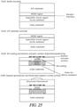
- Figs. 25 and 26 illustrate the major steps of a fabrication sequence used to fabricate the preferred implementation of the 1310 nm tunable short cavity laser in Fig. 7 .
- Processing of devices in a wavelength range of 650-2300 nm can proceed in a similar fashion, with the except that GaAs-based devices do not require the first wafer bonding step shown in Fig. 25 , since mirror and gain region can be epitaxially grown in one step.
- Fig. 25 and 26 illustrate the major steps of a fabrication sequence used to fabricate the preferred implementation of the 1310 nm tunable short cavity laser in Fig. 7 .
- Processing of devices in a wavelength range of 650-2300 nm can proceed in a similar fashion, with the except that GaAs-based devices do not require the first wafer bonding step shown in Fig. 25 , since mirror and gain region can be epitaxially grown in one step.
- Fig. 25 and 26 illustrate the major steps of a fabrication sequence used to fabricate the preferred implementation of the 13
- the first step 2510 involves wafer bonding of the MQW region epitaxially grown on an InP substrate to a GaAs/AlAs mirror structure epitaxially grown on a GaAs substrate. This process can be accomplished throught the application of pressure and about 570C temperature for about 15 minutes, as has been described in greater detail by prior art researchers in ( Black, A., Hawkins, A. R., Margalit, N. M. et al., "Wafer fusion: Materials issues and device results," IEEE Journal of Selected Topics in Quantum Electronics, 3(3), 943-951 (1997 )).
- the MQW and the mirror structure are joined at a wafer-bonded interface.
- the InP substrate is removed in a second step 2520 using an HCL-based etch stopping on an InGaAs stop etch layer.
- a sulfuric acid based etch then removes the stop-etch layer.
- the bottom MEMS contact which is preferably terminated with titanium to promote adhesion of germanium in a subsequent step, and anti-reflection coating are deposited and patterned, and holes are etched for oxidation of the GaAs/AlAs mirror structure. Oxidation converts the AlAs to Al x O y to create a highly reflecting mirror with six or severn periods.
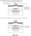
- a germanium sacrifical layer is deposited in a fourth step 2540, and the germanium is structured to have a curved surface in the region of light oscillation.
- Fig. 26 illustrates how in a 5 th series of steps 2550, the silicon nitride membrane layer, top actuator contact, and top suspended mirror are deposited and patterned on the germanium sacrificial layer.
- the top contact layer is preferably aluminum.
- the germanium sacrificial layer is released using Xenon Diflouride (XeF 2 ) gas to create a suspended structure with a rigid germanium support structure at the edges.
- XeF 2 Xenon Diflouride
- wire bond pads shown in Fig. 7 connecting with the top and bottom actuator metal, are deposited to complete processing before release. Processing after release is generally not advisable, as it can lead to collapse of the actuator. In many cases, it is preferable to dice and wire bond devices to a submount for packaging, prior to releasing the germanium membrane.
- the design of the gain region in the preferred embodiment of Fig. 7 is important for device performance.
- the quantum wells can be aligned with peaks of an optical standing wave to enhance gain through the well-known periodic gain effect, described in the prior art by ( Corzine, S. W., Geels, R. S., Scott, J. W. et al., "DESIGN OF FABRY-PEROT SURFACE-EMITTING LASERS WITH A PERIODIC GAIN STRUCTURE,” IEEE Journal of Quantum Electronics, 25(6), 1513-1524 (1989 )).
- periodic gain is that the wide spacing between quantum wells prevents strain accumulation and reduces the need for strain compensation.
- the ideal pump wavelength for the 1310 nm tunable VCSEL shown is in a range of about 850-1050 nm.
- three quantum wells can be placed on three separated standing wave peaks, and the region between them can be made of AlInGaAs substantially lattice-matched to InP, and of a composition that absorbs incoming pump radiation.
- the gain region is separated from the absorbing regions, and photo-generated carriers in the absorbing regions diffuse into gain region.
- the FSR of the structure can be increased by placing three quantum wells at a single standing wave peak. In this case, strain compensation of the compressively strained AlInGaAs wells with tensilely strained AlInGaAs may be required.
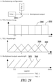
- Fig. 9 shows the static and dynamic tuning response of an ultra-widely tunable MEMS-VCSELs.
- the long-wavelength spectrum 910 at 1372 nm exhibits a completing mode at 1211 nm, illustrating the 161 nm FSR of the cavity.
- the curve 920 represents the time-averaged spectrum uner sinusoidal sweeping at 500 kHz. Both the static and dynamic response demomstrate continuous single-transvers and longitudinal mode lasing operation over a 150 nm span. FSR in the range of 140-170 nm for 1310 nm devices provides device tuning that is exceptionally well suited for swept source optical coherence tomography systems.
- a large FSR is desirable not only as a means to increase the tuning range of the laser but also as a means to reduce the duty factor of the laser such that additional tuning profiles from other tunable short-cavity lasers can be added as described later.
- the gain bandwidth of the laser is restricted to ⁇ 50% of the FSR, and the entire FSR is swept, then the laser automatically turns off for more than half the sweep, leaving room to interleave a sweep from another laser, or a time-delayed copy of the sweep, as described in for example ( Klein, T., Wieser, W., Eigenwillig, C. M. et al., "Megahertz OCT for ultrawide-field retinal imaging with a 1050nm Fourier domain mode locked laser," Optics Express, 19(4), 3044-30623062 (2011 )).
- the wide FSR structure producing the results of Fig. 9 employed can be characterized by the number of maxima in the optical standing wave formed between the mirrors during lasing operation.
- the results of Fig. 9 were produced by a structure with five standing wave maxima in the cavity between the bottom mirror and the suspended mirror. Futher reduction of cavity thickness to below five standing wave maxima can lead to larger FSR approaching 200 nm for a 1310 nm device.
- Fig. 8 shows the variation of refractive index vs.
- Fig. 8 represents the fully oxdized mirror and the periodic structure at the right of Fig. 8 represents the suspended dielectric mirror including the thicker first layer which is the silicon nitride membrane.
- the MQW gain region and airgap tuning region between the mirrors are also indicated in Fig. 8 .
- the features described in the preceding paragraph apply not only to VCSELs in the 1310 nm range but similar principles can be applied across the 1150-2500 nm wavelength range, which can use an InP-based gain region in conjunction with a GaAs-based mirror region.
- the 1200-1400 nm range is particularly important for many swept source optical coherence tomography applications, such as endoscopic applications, vascular imaging, and cancer imaging.
- the 1800-2500 nm range is important for gas spectroscopy. This latter range preferably uses compressively strained InGaAs quantum wells on Indium Phosphide substrates.
- Fig. 23 illustrates another MEMS-tunable VCSEL like that of Fig. 7 but instead configured to operate in a wavelength range around 1060 nm.
- this device employs a fully oxidized AlGaAs/Al x O y mirror 2310 as the bottom mirror.
- the aluminum content in the AlGaAs layers of this bottom mirror is preferably >10%, to prevent absorption of the pump beam in the optically pumped structure, which ideally has a pump wavelength around 850 nm.
- no wafer bonding is required, since the compressively strained InGaAs quantum wells in the gain region can be epitaxially grown on the same GaAs substrate as the fully oxidized mirror.
- a non-wafer-bonded structure like Fig. 23 can be configured with other quantum well compositions to access a range of wavelengths in a range from about 600 nm to about 1150 nm.
- InGaAs these include but are not limited to AlInGaP, AlInGaAs, InGaAsP, InGaP, AlGaAs, and GaAs.
- GaAs quantum wells would be used in about the 800-870 nm range, AlGaAs wells in about the 730-800 nm range, AlInGaP and InGaP in about the 600-730 nm range, and InGaAsP or AlInGaAs as alternative materials in about the 800-900nm range.
- the wavelength range of 700-1100 nm is of particular interest in SSOCT ophthalmic imaging and also oxygen sensing, and the range of about 990-1110 nm is of greatest interest for ophthalmology.
- periodic gain can be employed in the structure of Fig. 23 .
- a periodic gain structure with three InGaAs quantum wells 2320 at three standing wave peaks in the cavity, separated by GaAs barriers which absorb the pump radiation and generate electrons and holes which diffuse into the quantum wells.
- Typical quantum well widths are 6-12 nm and typical Indium percentage is about 20%.
- Quantum well widths greater than about 8 nm lead to a second confined quantum state and broadened gain.
- a structure using this approach generated the tuning results shown in Fig. 24 , illustrating a tuning range of 100 nm around 1060 nm.
- the FSR of this structure is around 100 nm or about 9.4% of the center wavelength. FSR can be increased to >10% as in the 1310 nm structure by placing all quantum wells on a single standing wave peak or by placing four quantum wells on two standing wave peaks. In these latter cases, strain compensation of the InGaAs with tensile-strained GaAsP, as described in the prior art on fixed wavelength VCSELs ( Hatakeyama, H., Anan, T., Akagawa, T.
- Both the structure of Fig. 7 and that of Fig. 24 achieve a tuning range that is >90% of the FSR of the device, as shown in the associated results of Figs. 9 and 24 respectively.
- a suppression of transverse modes manifesting themselves as a shoulder 1-3 nm away from the main peak, which is generally >40 dB below the main peak.
- the transverse mode suppression can be increased to >45 dB across the tuning range if the pump beam is well-aligned along the optical axis of the half-symmetric cavity of Fig. 1 .
- tunable emission in about the 2000-2500 nm mid-infrared range could be obtained using materials on GaSb substrates, as prior art researchers have done with fixed wavelength VCSELs in ( Kashani-Shirazi, K., Bachmann, A., Boehm, G. et al., "MBE growth of active regions for electrically pumped, cw-operating GaSb-based VCSELs," Journal of Crystal Growth, 311(7), 1908-1911 (2009 )).
- a tunable short-cavity laser according to an embodiment of the present invention operating in the 400-550 nm range could be realized using materials grown on GaN substrates as described by researchers making fixed wavelength VCSELs ( Higuchi, Y., Omae, K., Matsumura, H. et al., "Room-Temperature CW Lasing of a GaN-Based Vertical-Cavity Surface-Emitting Laser by Current Injection," Applied Physics Express, 1(12), (2008 )).
- VCSELs Higuchi, Y., Omae, K., Matsumura, H. et al., "Room-Temperature CW Lasing of a GaN-Based Vertical-Cavity Surface-Emitting Laser by Current Injection," Applied Physics Express, 1(12), (2008 )
- Implementation of embodiments of the present invention in the visible range of 400-700 nm range has application in optical metrology tools and biological and medical spectroscopy.
- the optical pump wavelength is preferably in a range of about 400 nm to about 600 nm.
- the preferred pump wavelength is in a range of about 600-1000 nm.
- the preferred pump wavelength is in a range of about 700-1200 nm.
- the preferred pump wavelength is in a range of about 1000-2000 nm.
- Fig. 14 illustrates an example top mirror designed reflectivity for a tunable short-cavity laser configured to emit in the range of 1200-1400 nm, with an optical pump at 1050 nm.
- the top mirror can be made to have minimal reflectivity 1410 at the pump wavelength at 1050 nm, while having high reflectivity 1420 at the desired 1200-1400 nm emission wavelength range.
- FIG. 27 is a MEMS-tunable VCSEL with GaAs-based MQW gain region 2710 and a fully oxidized mirror, as in the 1060 nm example of Fig. 24 .
- the bottom MEMS contact 2740 also functions as the top laser diode contact.
- the confinement of optical carriers is accomplished by the limited lateral extent of the optical pump beam, while in an electrically pumped structure a current aperture 2720 must be provided.
- This aperture 2720 is usually provided by another partially oxidized layer above the fully oxidized mirror, as shown in Fig. 27 .
- the current aperture could also be provided by a patterned and buried tunnel junction, as has been employed by other researchers. In both cases, care must be taken to engineer the spreading resistance to avoid current crowding, as has been described by prior art researchers in fixed wavelength VCSELs ( Scott, J. W., Geels, R. S., Corzine, S. W.
- the combination of implant passivation 2730 and oxide current aperturing 2720 enables electrical pumping of the structure.
- Current conduction proceeds from the middle MEMS contact 2740 through the current aperture 2720, and around the fully oxidized region of the bottom mirror to a backside substrate contact 2750.
- Carrier recombination in the MQW region which is preferably comprised of three strain-compensated InGaAs/GaAsP quantum wells, produces gain for lasing.
- This output power shaping can be accomplished in a variety of ways.
- One method is by controlling the shape of the top mirror reflectivity spectrum. Generally, regions of lower reflectivity allow more light out of the optical cavity, while regions of higher reflectivity allow less light out of the optical cavity.
- a target spectral shape or power variation across the wavelength range can be a Gaussian shape.
- Fig. 22 illustrates examples of several spectral shapes that have been achieved in the MEMS-VCSEL implementation of Fig. 7 , by adjusting the reflectivity spectrum of the suspended top mirror. These spectra range from power peaked at both edges, power peaked at the blue edge, and power peaked at the red edge. Additional spectral shapes can be achieved by the same method.
- Another way of changing the spectral shape is to control the pump energy into the gain region dynamically during wavelength tuning.
- this can be controlling the pump energy into the device, and in the case of an electrically pumped device the drive current would be controlled. Shaping of the pump energy can also improve thermal management of the device.
- the deformable dielectric membrane is preferably made of silicon nitride, and a tensile stress of 100-1000 MPa is preferred to give a substantially increased resonant frequency relative to a no-stress design, and to minimize bowing of the membrane upon release.
- resonant frequency we are referring to the lowest order mechanical mode of the device, which corresponds to the desired "piston" motion of the actuator. This is an important parameter of the device performance.
- One preferred actuator geometry is a central plate with supporting arms, as shown in Fig. 7 , Fig. 12 , and Fig. 23 .
- actuator diameter the actuator diameter, central plate diameter, arm width, and suspended mirror diameter, as shown in Fig. 23 .
- FIG. 12 shows pictures of a sampling of actuator geometries resulting in the frequency responses of Fig. 10 .
- Fig. 12 top-view pictures of several MEMS tunable VCSEL structures having four or eight supporting struts 1210.
- Fig. 10 shows the tuning of a MEMS-VCSEL wavelength as a function of drive frequency applied to the MEMS-actuated airgap tuning mechanism. As shown, the resonant frequencies are in a range of about 200 kHz to about 500 kHz, and the 6 dB bandwidths of the fastest devices are approaching 1 MHz.
- damping of the actuator manifested by varying amounts of peaking at resonance.
- the damping is primarily caused by squeeze-film damping, which represents interaction with viscous air.
- squeeze-film damping represents interaction with viscous air.
- the squeeze-film damping goes up, flattening the frequency response.
- a flat wide frequency response is desirable for variable speed drive, and for linearization of drive through multiple harmonics.
- the damping of the MEMS actuator through a variety of methods, including changing the actuator area or shape to change interaction with viscous air, changing the background gas composition or gas pressure, which further changes the contribution of squeeze-film damping, changing the airgap thickness, and changing the size of holes or perforations in the actuator to change the regime of fluid flow through the holes from a turbulent to a non-turbulent regime. Additionally, annealing the actuator can change the stress of various materials in the actuator, which will have an effect on damping.
- the frequency responses represented by Fig. 10 are representative and not limiting.
- the resonance frequency can be increased by stiffening the membrane through increased tensile stress, increased thickness (for example 5/4 wavelength), reduced suspended mirror diameter and thickness, or shortened arms, such that 6-dB bandwidths in excess of 2 MHz can be achieved, as can be calculated by those skilled in the art of finite element modeling.
- resonant frequency can be decreased well below 100 kHz by changing the same parameters in the opposite direction.
- other geometries are possible, such as a spiral arm geometry, which reduces resonant frequency, or a perforated membrane without clearly delineated supporting struts. Referring to Fig. 12 , if the diameter of the central plate 1220 is expanded to the outer ring 1230 actuator diameter, and perforations are added, we achieve a perforated membrane without clearly delineated supporting struts.
- the silicon nitride membrane discussed above is highly insulating, and may therefore be prone to charging and electrostatic drift. Introducing a small amount of electrical conductivity in the membrane can reduce the propensity to charging. For silicon nitride, this electrical conductivity can be introduced by using a non-stoichiometric silicon-rich film, or by doping the silicon nitride film with silicon.
- the tuning results presented in Figs. 9 and 24 indicate the voltages required to tune the device, noted alongside the spectra. These voltages range up to about 65 V for full tuning over on FSR, corresponding to a membrane deflection of about half the center wavelength or about 650 nm for 1310 nm devices and 525 nm for 1050 nm devices. These voltages are associated with the MEMS actuator dimensions and silicon nitride stress levels indicated above, and with reference to Figs. 10 and 12 , along with a nominal zero-voltage airgap in the range of about 1.6 ⁇ m.
- Figs. 1 and 2 A number of additional structural and performance features of an embodiment of the present invention can be understood with further reference to Figs. 1 and 2 .
- the intensity vs. wavelength profile shown in Fig. 2 , to be free of periodic variation.
- the present disclosure describes a short-cavity tunable laser with a ripple that is less than about 1% of an average power.
- the term "ripple" is commonly used to describe these variations. Depending on the spectral period of this ripple, and depending on the application, it may have varying degrees of adverse effect.
- ripple of a particular spectral period having an amplitude of 1% or more relative to an average power can manifest itself as a spurious reflector at an apparent distance in an SSOCT image.
- Ripple is typically caused by spurious reflections outside the laser cavity. These reflections can come from coupling lenses or other optical elements in the optical system, or they can come from substrate reflections in a vertical cavity laser. For example, in the laser of Fig. 7 , reflections coming from below the second mirror, such as from the bottom of the GaAs substrate 770 on which this device is disposed, can cause ripple.
- the substrate reflection amplitude can be suppressed by various means, including but not limited to increasing the reflectivity of the second mirror, introducing loss through dopants in the substrate, increasing substrate thickness, or roughening the backside of the substrate to increase scattering.
- An optimal grit for substrate roughening to increase scattering is a grit size >30 ⁇ m in the range of 900-1400 nm tunable emission.
- use of a fully oxidized bottom mirror having 7 or more periods, which has a theoretical lossless reflectivity of >99.5%, can suppress ripple to ⁇ 1% levels.
- Another important performance feature of an embodiment of the present invention is operation in a fixed polarization state throughout a tuning range of the wavelength swept emission.
- Operation in a single polarization state is important if operating with any polarization-sensitive components in the optical system, such as polarization-selective optical amplifiers.
- Such systems may also employ the polarization stable device according to an embodiment of the present invention in combination with polarization maintaining fiber.
- Polarization switching over the emission wavelength range can cause power dropouts or image artifacts in an SS-OCT system, and compromise dynamic coherence length. Having a well-defined polarization state would also allow a laser system to be constructed that requires alternating polarization states.
- Operation in a single polarization state throughout a tuning range of the device can be accomplished in a variety of ways.
- One way is to introduce one or more nanowires integral with the optical cavity of the device. With respect to Fig. 7 , this nanowire can be disposed on top of the MQW gain region 780 adjacent the tunable airgap, in the center of the optical path. Alternatively it could be placed on top of the suspended mirror.
- a nanowire is an element which can cause polarization-dependent scattering or absorption of light. Typical dimensions might be 50 nm wide, several microns long, and 10 nm thick.
- the nanowire might be constructed of metal or may simply be a refractive index perturbation.
- Having a grid of nanowires creates greater loss anisotropy, but also increases loss for the preferred polarization. So in for example a VCSEL cavity, excess loss introduced in the preferred polarization should be ⁇ 0.1%. This suggests one or a very small number of nanowires.
- the nanowire In the case of a VCSEL or VCL, ideally the nanowire should be aligned with the crystal axes of the semiconductor on which the VCSEL is disposed. This typically means the [110] direction or perpendicular to the [110] direction for wafers grown on (100) or near (100) orientation. The reason for this is that a weak polarization selection effect exists to align the VCL polarization along one of the crystal axes, and any further polarization control method should strive to add to rather than compete with this effect.
- polarization control include introduction of anisotropic stress, as in ( Matsui, Y., Vakhshoori, D., Peidong, W. et al., "Complete polarization mode control of long-wavelength tunable vertical-cavity surface-emitting lasers over 65-nm tuning, up to 14-mW output power," IEEE Journal of Quantum Electronics, 39(9), 1037-10481048 (2003 )), lateral current injection as described in fixed wavelength VCSELs ( Zheng, Y., Lin, C.-H., and Coldren, L.
- oxidation 1310 proceeds outward from two etched holes 1320, and oxidation fronts meet along a line shown by the dashed line 1330 in the figure.
- dashed line 1330 is a 5 nm dip, which forms a refractive index nanowire, which can select the VCSEL polarization.
- the refractive index nanowire of Fig. 13 will be aligned with the crystal axes as long as the holes are aligned with the crystal axes.
- the tunable short-cavity laser described here can be combined in array form to generate an aggregate tunable laser source with enhanced optical properties.
- the array can be fabricated in monolithic form.
- a first tunable short cavity laser TCSL 1 and a second tunable short-cavity laser TCSL 2 are multiplexed on to a common optical path, using a beam splitter, fiber coupler or other know combining element 2810.
- Each TCSL is driven to have a bidirectional tuning over its tuning range, as shown by the solid wavelength trajectory 2820 in Fig.
- each laser is repetitively scanned at a repetition period T, but the scan of TCSL 2 is time-delayed relative to that of TCSL 1 by half the repetition period.
- the pump energy 2840, 2850 (either electrical or optical pump) for each of the two TCSLs is turned off during the backward wavelength scan such that only the forward or front of half of the wavelength scan, when pump energy is non-zero, emits laser radiation.
- the FSR is much larger than the gain bandwidth of the supporting material, scanning the tuning element beyond the material gain bandwidth will automatically shut off the laser without having to turn off the pump energy.
- the wavelength trajectory of the multiplexed output is shown in Fig. 28D , comprising components from both TCSL 1 (solid) 2860 and TCSL 2 (dashed) 2870, and illustrating unidirectional scanning at a new repetition period T/2 which is half the original period T of each TCSL.
- the sweep rate has been multiplied by a factor of two.
- the same principle could be applied to N lasers and multiplication of the sweep rate by a factor of N.
- interleaving TCSLs can also be used for more than multiplying sweep rate, but also for multiplying tuning range, interleaving different tuning ranges, tuning speeds, or tuning trajectories, or a for a variety of other purposes evident to those skilled in the art of SSOCT, spectroscopy, communications, or optical detection.
- the tunable short-cavity laser described thus far can be combined with an optical amplifier to create an amplified tunable source with increased output power and other advantageous properties for imaging.
- the amplifier can be a semiconductor amplifier, a fiber amplifier such as a praseodymium-doped fiber amplifier for operation in a window around 1300 nm, an Ytterbium-doped amplifier for operation in a window around 1050 nm , a Fluoride-doped extended bandwidth fiber amplifier near 1050 nm, or any kind of optical amplifier.
- the use of an amplifier can also enable the interleaving scheme above, wherein a high extinction ratio optical amplifier can be used to turn on one source at the appropriate time, instead of turning off the pump energy to that source.
- a tunable short cavity laser 1510 according an embodiment of the present invention emits an input tunable radiation 1520 directed to an input side of the optical amplifier 1530.
- This input tunable radiation has an input average power, input power spectrum, input wavelength range, and input center wavelength.
- the amplifier amplifies the input tunable radiation to generation an output tunable radiation having an output average power, output center wavelength, output wavelength range, and output power spectrum.
- the amplifier is operated in a saturated regime, as is well-known to those skilled in the art of optical amplifiers.
- the saturated regime can suppress noise fluctuations present in the input tunable radiation, and can also provide advantageous spectral shaping in which a full-width at half-maximum (FWHM) of the output tunable radiation can exceed a FWHM of the output tunable radiation.
- FWHM full-width at half-maximum
- An example of this is shown in Fig. 21 , in which the amplified tunable spectrum 2110 has a wider FWHM than the input tunable radiation 2120 from the tunable short cavity laser.
- the optical amplifier is a semiconductor quantum well amplifier, which can provide low noise, wide gain-bandwidth, and high gain. Semiconductor quantum well amplifiers can also provide very high extinction ratio >40 dB, which can be used as a switch to gate devices on and off as described above.
- the quantum well is preferably configured to have two confined quantum states to support a wider gain bandwidth.
- Fig. 16 illustrates amplified spontaneous emission from a dual quantum state semiconductor optical amplifier at 1310 nm, comprising three AlInGaAs compressively strained quantum wells, illustrating a hump 1610 at the shorter end of the spectrum corresponding to second quantum state widening of the spectrum.
- the 3-dB spectral width of this amplified spontaneous emission (ASE) is 110 nm, suggesting a 3 dB small signal gain bandwidth of similar value.
- the semiconductor optical amplifier can be configured to be polarization sensitive, by using all compressively strained or tensile-strained quantum wells, or polarization insensitive by using both types of strain in a single structure to provide gain at all polarizations.
- the center wavelength of the input tunable radiation is at a longer wavelength than a center wavelength of amplified spontaneous emission (ASE) emitted by the amplifier.
- ASE amplified spontaneous emission
- the amplifier ASE is typically blue-shifted relative to the amplifier gain spectrum, so this configuration brings the spectrum of input tunable radiation into more optimal alignment with the amplifier gain spectrum.
- varying the alignment of the amplifier ASE relative to the input power spectrum can provide advantageous spectral shaping.
- Fig. 15 The basic configuration of Fig. 15 can be augmented with various forms of filtering to create a lower noise amplified swept source. Many swept source laser application in metrology, spectroscopy, and biophotonics would benefit from the suppression of broadband ASE, and an improvement in side mode suppression.
- the addition of an additional tunable spectral filter to the system, either internal to the laser cavity, between the laser and amplifier, or at the output of the system is one means of providing improved performance in this regard.
- the amplifier shown in Fig. 15 is a tunable resonant amplifier, such as a vertical cavity amplifier described by ( Cole, G. D., Bjorlin, E. S., Chen, Q.
- a synchronously tuned optical filter 1710 whose passband is aligned at all times with the wavelength of the input tunable radiation, is placed after the broadband optical amplifier 1720 to reduce residual ASE noise and improve a signal to noise ratio of the amplified tunable radiation.
- the same synchronously tuned optical filter 1810 is placed between the tunable short cavity laser 1830 and the optical amplifier 1820, to improved a side-mode suppression of the input tunable radiation prior to amplification.
- Fig. 19 Another configuration is illustrated in Fig. 19 , where two amplification stages 1910, 1920 are used. These can be implement as two separate amplifiers, or as a single waveguide amplifier with split amplifier contacts.
- the use of two amplification stages 1910, 1920 provides further flexibility in spectral shaping. For example, the gain spectrum of the two amplifiers can be shifted relative to each other, either by biasing identical epitaxial structures differently, or by using different epitaxial structures in the two amplifiers.
- the use of two amplification stages can also create higher gain and greater output power.
- Fig. 20 illustrates yet another two-stage amplifier configuration in which a synchronously tuned optical amplifier 2030 is placed between the two amplifier stages 2010, 2020. This will serve to provide an improved signal to noise ratio of the output tunable radiation.
- the preferred range of input average powers is about 0.05-2 mW, resulting in a preferred range of output average powers of about 10-120 mW.
- the exact numbers depend on the gain and saturation power of the amplifier, but this range generally produces amplified tunable radiation with good signal to noise ratio for optical systems.
- the basic configuration of the tunable short-cavity laser in combination with an amplifier can be realized with semiconductor optical amplifiers employing a variety of materials appropriate for a variety of wavelength ranges.
- the amplifier can operate in the 1200-1400 nm range appropriate for SSOCT and water vapor spectroscopy. In this range, use of an AlInGaAs or InGaAsP quantum well on InP produces the required gain.
- the amplifier can operate in about the 800-1100 nm range appropriate for ophthalmic SSOCT, employing at least one compressively strained InGaAs quantum well.
- a system for SSOCT can employ a tunable laser comprising the tunable short-cavity laser described above, in combination with a means for splitting tunable radiation from the tunable laser to a reference path and a sample path, and an optical detector configured to detect an interference signal between light reflected from said sample and traversing said reference path. Signal processing of this interference signal can then be used to reconstruct structural or compositional information about he sample, as is well-know to those skilled in the art of SSOCT.
- a system for optical spectroscopy can employ the tunable short-cavity laser described, in conjunction with an optical detector, to measure an absorption, transmission, scattering, or reflection spectrum of a sample, which can be a solid, liquid, gas, plasma, or any substance in any state of matter.
- the variable tuning speed of the tunable short cavity laser can be used to scan across an optical spectrum at variable speed, slowing down information rich regions and speeding up in less-information rich regions, to obtain a desired signal to noise ratio while minimizing measurement time.
- the tunable short cavity laser described can, in combination with a dispersive optical element, be employed in a system for optical beam steering.
- a dispersive optical element For example, it is well-known that the diffraction angle of a grating is a function of the wavelength of input tunable radiation. Thus, tuning the radiation will scan the diffraction angle and achieve optical beam steering.
- Other dispersive elements such as prisms can also be employed.
- An embodiment of the present invention can also be used to create a tunable oscillator, by beating the tunable output of the short-cavity laser with a fixed wavelength reference laser.
- This beating can be accomplished by, for example, an optical detector that responds to incident optical power. If two collinear laser beams impinge on this detector, the detector output will oscillate at the difference in optical frequencies between the two laser beams, provided that difference frequency is within the detector bandwidth. As one laser is tuned, this difference frequency will also tune, creating a tunable oscillator down-shifted from optical frequencies to lower frequencies.
Claims (2)
- Verstärkte abstimmbare Laserquelle, die einen abstimmbaren Laser und einen optischen Verstärker umfasst und konfiguriert ist, um eine abstimmbare Eingangsstrahlung (1520), die ein Eingangsleistungsspektrum, eine Eingangsmittenwellenlänge, einen Eingangswellenlängenbereich und eine durchschnittliche Eingangsleistung aufweist, optisch an eine Eingangsseite eines optischen Halbleiterverstärkers (1530) gekoppelt ist, der mindestens einen Quantentopf umfasst, und eine abstimmbare Ausgangsstrahlung, die ein Ausgangsleistungsspektrum, eine Ausgangsmittelwellenlänge, einen Ausgangswellenlängenbereich und eine durchschnittliche Ausgangsleistung, die von einer Ausgangsseite des optischen Verstärkers ausgeht, aufweist, zu emittieren,wobei der optische Verstärker konfiguriert ist, um die abstimmbare Eingangsstrahlung zu verstärken und die abstimmbare Ausgangsstrahlung zu erzeugen;wobei der abstimmbare Laser (100) konfiguriert ist, um die abstimmbare Eingangsstrahlung zu erzeugen;wobei der abstimmbare Laser umfassteinen optischen Resonator mit einem ersten und einem zweiten Spiegel (130, 140);einen Verstärkungsbereich (110), der zwischen dem ersten und dem zweiten Spiegel (130, 140) eingefügt ist;einen Abstimmbereich (120); undMittel zum Einstellen einer optischen Weglänge des Abstimmbereichs;wobei:ein freier Spektralbereich (FSR) des optischen Resonators 5% der Eingangsmittenwellenlänge überschreitet;der abstimmbare Laser im Wesentlichen in einer einzigen longitudinalen und transversalen Mode über den Wellenlängenbereich arbeitet;das Mittel zum Einstellen einer optischen Weglänge einen Wellenlängen-Abstimmungsfrequenzgang mit einer 6-dB-Bandbreite von mehr als ungefähr 1 kHz hat; undder optische Verstärker ein resonant abstimmbarer optischer Verstärker ist, der konfiguriert ist, um synchron mit der abstimmbaren Eingangsstrahlung abgestimmt zu werden, so dass das Durchlassband des optischen Verstärkers jederzeit mit der Wellenlänge der abstimmbaren Eingangsstrahlung abgestimmt ist.
- Verstärkte abstimmbare Laserquelle nach Anspruch 1, wobei der resonante abstimmbare optische Verstärker ein optischer Verstärker mit vertikalem Resonator ist.
Applications Claiming Priority (2)
| Application Number | Priority Date | Filing Date | Title |
|---|---|---|---|
| US201261676712P | 2012-07-27 | 2012-07-27 | |
| PCT/US2013/052411 WO2014018939A2 (en) | 2012-07-27 | 2013-07-26 | Amplified widely tunable short cavity laser |
Publications (3)
| Publication Number | Publication Date |
|---|---|
| EP2878048A2 EP2878048A2 (de) | 2015-06-03 |
| EP2878048A4 EP2878048A4 (de) | 2016-06-01 |
| EP2878048B1 true EP2878048B1 (de) | 2022-02-09 |
Family
ID=49997881
Family Applications (5)
| Application Number | Title | Priority Date | Filing Date |
|---|---|---|---|
| EP13823016.4A Active EP2878047B1 (de) | 2012-07-27 | 2013-07-26 | Mems-abstimmbarer kurzer resonator |
| EP13822317.7A Active EP2878046B1 (de) | 2012-07-27 | 2013-07-26 | Einstellbarer laser mit kurzem resonator für einen quantenschacht |
| EP13823419.0A Active EP2878048B1 (de) | 2012-07-27 | 2013-07-26 | Verstärkter breit abstimmbarer laser mit kurzem resonator |
| EP13823861.3A Active EP2878049B8 (de) | 2012-07-27 | 2013-07-26 | Abstimmbarer lasersensor mit kurzem resonator |
| EP13822215.3A Active EP2878045B1 (de) | 2012-07-27 | 2013-07-26 | Polarisationsstabiler und weitgehend einstellbarer laser mit kurzem resonator |
Family Applications Before (2)
| Application Number | Title | Priority Date | Filing Date |
|---|---|---|---|
| EP13823016.4A Active EP2878047B1 (de) | 2012-07-27 | 2013-07-26 | Mems-abstimmbarer kurzer resonator |
| EP13822317.7A Active EP2878046B1 (de) | 2012-07-27 | 2013-07-26 | Einstellbarer laser mit kurzem resonator für einen quantenschacht |
Family Applications After (2)
| Application Number | Title | Priority Date | Filing Date |
|---|---|---|---|
| EP13823861.3A Active EP2878049B8 (de) | 2012-07-27 | 2013-07-26 | Abstimmbarer lasersensor mit kurzem resonator |
| EP13822215.3A Active EP2878045B1 (de) | 2012-07-27 | 2013-07-26 | Polarisationsstabiler und weitgehend einstellbarer laser mit kurzem resonator |
Country Status (6)
| Country | Link |
|---|---|
| US (7) | US9843159B2 (de) |
| EP (5) | EP2878047B1 (de) |
| JP (5) | JP6328112B2 (de) |
| CN (7) | CN104718673B (de) |
| CA (5) | CA2880034C (de) |
| WO (5) | WO2014018942A1 (de) |
Families Citing this family (44)
| Publication number | Priority date | Publication date | Assignee | Title |
|---|---|---|---|---|
| US9391423B2 (en) * | 2008-12-16 | 2016-07-12 | Massachusetts Institute Of Technology | Method and applications of thin-film membrane transfer |
| CN104718673B (zh) * | 2012-07-27 | 2017-11-14 | 统雷有限公司 | 可调谐短腔激光器传感器 |
| CA2880038C (en) * | 2012-07-27 | 2021-06-01 | Thorlabs, Inc. | Agile imaging system |
| JP6450743B2 (ja) * | 2013-03-15 | 2019-01-09 | プレビウム リサーチ インコーポレイテッド | 可変レーザアレイシステム |
| JP6512666B2 (ja) * | 2013-11-13 | 2019-05-15 | ダンマークス テクニスク ユニバーシテットDanmarks Tekniske Universitet | 圧縮光パルスの発生方法 |
| EP2947729A1 (de) * | 2014-05-21 | 2015-11-25 | Universite De Montpellier | Oberflächenemittierende Laservorrichtungen mit vertikalem externem Resonator zur Ermöglichung von hoher Kohärenz, hoher Leistung und großer Abstimmbarkeit |
| FR3022684B1 (fr) * | 2014-06-23 | 2017-10-27 | Commissariat Energie Atomique | Dispositif a membrane a germanium sous contrainte |
| US9312662B1 (en) | 2014-09-30 | 2016-04-12 | Lumentum Operations Llc | Tunable laser source |
| JP6685701B2 (ja) * | 2014-12-26 | 2020-04-22 | キヤノン株式会社 | 面発光レーザ、情報取得装置、撮像装置、レーザアレイ及び面発光レーザの製造方法 |
| EP3282921B1 (de) | 2015-04-16 | 2022-02-16 | Gentuity LLC | Mikrooptische sonden für die neurologie |
| JP6576092B2 (ja) | 2015-04-30 | 2019-09-18 | キヤノン株式会社 | 面発光レーザ、情報取得装置及び撮像装置 |
| DE102015108876B3 (de) * | 2015-06-04 | 2016-03-03 | Otto-Von-Guericke-Universität Magdeburg, Ttz Patentwesen | Lichtemittierendes Gruppe-III-Nitrid basiertes Bauelement |
| EP3344126A4 (de) | 2015-08-31 | 2019-05-08 | Gentuity LLC | Abbildungssystem mit bildgebender sonde und abgabevorrichtungen |
| JP6824605B2 (ja) * | 2015-11-12 | 2021-02-03 | キヤノン株式会社 | 増幅素子、光源装置及び撮像装置 |
| JP6679340B2 (ja) * | 2016-02-22 | 2020-04-15 | キヤノン株式会社 | 光干渉断層計 |
| WO2018052910A1 (en) * | 2016-09-15 | 2018-03-22 | Flir Systems Ab | Detection of gas on a scene |
| RU2704214C1 (ru) * | 2016-12-13 | 2019-10-24 | Федеральное государственное бюджетное учреждение науки Физико-технический институт им. А.Ф. Иоффе Российской академии наук | Вертикально-излучающий лазер с внутрирезонаторными контактами и диэлектрическим зеркалом |
| GB201701829D0 (en) * | 2017-02-03 | 2017-03-22 | Norwegian Univ Of Science And Tech (Ntnu) | Device |
| US10641733B2 (en) * | 2017-03-20 | 2020-05-05 | National Technology & Engineering Solutions Of Sandia, Llc | Active mechanical-environmental-thermal MEMS device for nanoscale characterization |
| US9985414B1 (en) | 2017-06-16 | 2018-05-29 | Banner Engineering Corp. | Open-loop laser power-regulation |
| WO2019003627A1 (ja) * | 2017-06-28 | 2019-01-03 | ソニー株式会社 | 発光素子及びその製造方法 |
| US10714893B2 (en) | 2017-07-17 | 2020-07-14 | Thorlabs, Inc. | Mid-infrared vertical cavity laser |
| EP3444634B1 (de) * | 2017-08-17 | 2024-05-01 | ams AG | Halbleiterbauelement und verfahren für laufzeitmessungen |
| WO2019108598A1 (en) | 2017-11-28 | 2019-06-06 | Gentuity, Llc | Imaging system |
| JP6908131B2 (ja) * | 2017-12-25 | 2021-07-21 | 日本電気株式会社 | 光ビーム制御器およびこれを用いた光干渉断層撮像器 |
| DE102018109542B4 (de) | 2018-04-20 | 2022-08-04 | OSRAM Opto Semiconductors Gesellschaft mit beschränkter Haftung | Licht emittierendes bauelement und verfahren zur herstellung eines licht emittierenden bauelements |
| US10951009B2 (en) | 2018-05-11 | 2021-03-16 | Excelitas Technologies Corp. | Tunable VCSEL polarization control through dissimilar die bonding |
| JP7443248B2 (ja) | 2018-05-11 | 2024-03-05 | エクセリタス テクノロジーズ コーポレイション | 幾何学的分離を採用する光ポンピングチューナブルvcsel |
| US11721953B2 (en) | 2018-10-08 | 2023-08-08 | Thorlabs, Inc. | Electrically pumped vertical cavity laser |
| JP7190865B2 (ja) * | 2018-10-18 | 2022-12-16 | スタンレー電気株式会社 | 垂直共振器型発光素子 |
| CN109638644A (zh) * | 2019-01-25 | 2019-04-16 | 清华-伯克利深圳学院筹备办公室 | 一种扫频光源及其制作方法 |
| KR20200095395A (ko) | 2019-01-31 | 2020-08-10 | 삼성전자주식회사 | 유기금속 화합물 및 이를 포함한 유기 발광 소자 |
| EP3689888B1 (de) * | 2019-01-31 | 2021-09-22 | Samsung Electronics Co., Ltd. | Organometallische verbindung und organische lichtemittierende vorrichtung damit |
| WO2020227632A1 (en) * | 2019-05-08 | 2020-11-12 | Michigan Aerospace Corporation | Tunable optical resonator for lidar applications |
| FR3095893A1 (fr) * | 2019-05-09 | 2020-11-13 | Commissariat A L'energie Atomique Et Aux Energies Alternatives | dispositif optoélectronique comportant une portion centrale contrainte en tension suivant un premier axe et polarisee électriquement suivant un deuxième axe |
| CN110165550A (zh) * | 2019-05-31 | 2019-08-23 | 度亘激光技术(苏州)有限公司 | 一种分布布拉格反射镜的制备方法及垂直腔面发射激光器 |
| CN110793941A (zh) * | 2019-10-10 | 2020-02-14 | 成都贝瑞光电科技股份有限公司 | 一种智能分辨激光光学层析成像方法的系统 |
| CN111146688A (zh) * | 2019-12-24 | 2020-05-12 | 江西德瑞光电技术有限责任公司 | 一种电泵浦垂直外腔面发射激光器芯片及其制备方法 |
| WO2021240334A1 (en) | 2020-05-29 | 2021-12-02 | Ricoh Company, Ltd. | Optical device |
| US11609116B2 (en) | 2020-08-27 | 2023-03-21 | Banner Engineering Corp | Open-loop photodiode gain regulation |
| CN114499673A (zh) * | 2020-11-12 | 2022-05-13 | 莫列斯有限公司 | 光放大器模块及其增益控制方法 |
| CN112903613B (zh) * | 2021-02-24 | 2022-11-08 | 南昌大学 | 一种基于Labview的瞬态吸收光谱控制系统设计方法 |
| WO2023158635A1 (en) * | 2022-02-16 | 2023-08-24 | Vijaysekhar Jayaraman | Widely tunable frequency doubled light source |
| WO2024044567A2 (en) * | 2022-08-22 | 2024-02-29 | The Regents Of The University Of California | Iii-nitride-based vertical cavity surface emitting laser (vcsel) with a dielectric p-side lens and an activated tunnel junction |
Family Cites Families (86)
| Publication number | Priority date | Publication date | Assignee | Title |
|---|---|---|---|---|
| JPH01170084A (ja) | 1987-12-25 | 1989-07-05 | Nippon Telegr & Teleph Corp <Ntt> | 集積型光アンプ素子 |
| US5331658A (en) * | 1992-08-26 | 1994-07-19 | Motorola, Inc. | Vertical cavity surface emitting laser and sensor |
| DE4314486C2 (de) * | 1993-05-03 | 1998-08-27 | Heidenhain Gmbh Dr Johannes | Absolutinterferometrisches Meßverfahren sowie dafür geeignete Laserinterferometeranordnung |
| EP1315027A3 (de) * | 1995-09-20 | 2004-01-02 | Mitsubishi Materials Corporation | Optisches Umwandlungsverfahren mit einkristallinem Lithiumtetraborat |
| JP2904101B2 (ja) | 1996-03-15 | 1999-06-14 | 日本電気株式会社 | 雑音除去機能付き光増幅装置 |
| JP3570094B2 (ja) | 1996-07-10 | 2004-09-29 | 富士通株式会社 | 面発光半導体レーザ及びその製造方法及び波長可変方法 |
| JP3765030B2 (ja) | 1997-07-02 | 2006-04-12 | 日本光電工業株式会社 | ガスセンサ用パッケージ |
| AU9472298A (en) * | 1997-09-05 | 1999-03-22 | Micron Optics, Inc. | Tunable fiber fabry-perot surface-emitting lasers |
| JP2002500446A (ja) * | 1997-12-29 | 2002-01-08 | コアテック・インコーポレーテッド | マイクロエレクトロメカニカル的に同調可能な共焦型の垂直キャビティ表面放出レーザ及びファブリー・ペローフィルタ |
| US5991326A (en) * | 1998-04-14 | 1999-11-23 | Bandwidth9, Inc. | Lattice-relaxed verticle optical cavities |
| US6154471A (en) | 1999-02-22 | 2000-11-28 | Lucent Technologies Inc. | Magnetically tunable and latchable broad-range semiconductor laser |
| DE60041742D1 (de) * | 1999-02-26 | 2009-04-23 | Furukawa Electric Co Ltd | Halbleiterlaser |
| DE60029554T2 (de) | 1999-06-03 | 2007-07-12 | Koninklijke Philips Electronics N.V. | Halbleiterbauelement mit hochspannungselement |
| US6181717B1 (en) * | 1999-06-04 | 2001-01-30 | Bandwidth 9 | Tunable semiconductor laser system |
| US20020048301A1 (en) | 1999-07-30 | 2002-04-25 | Peidong Wang | Single mode operation of microelectromechanically tunable, half-symmetric, vertical cavity surface emitting lasers |
| US6594022B1 (en) * | 1999-08-23 | 2003-07-15 | Coretek, Inc. | Wavelength reference device |
| US6735234B1 (en) | 2000-02-11 | 2004-05-11 | Giga Tera Ag | Passively mode-locked optically pumped semiconductor external-cavity surface-emitting laser |
| US6373632B1 (en) * | 2000-03-03 | 2002-04-16 | Axsun Technologies, Inc. | Tunable Fabry-Perot filter |
| US6744805B2 (en) | 2000-04-05 | 2004-06-01 | Nortel Networks Limited | Single mode operation of microelectromechanically tunable, half-symmetric, vertical cavity surface emitting lasers |
| CN1222124C (zh) | 2000-07-10 | 2005-10-05 | Mpb技术有限公司 | 用于在光纤通信系统中生长分布式喇曼放大的级联泵浦系统和方法 |
| GB2369929A (en) | 2000-12-08 | 2002-06-12 | Univ Southampton | Semiconductor laser device |
| JP2002204026A (ja) | 2000-12-28 | 2002-07-19 | Daido Steel Co Ltd | 面発光デバイス |
| DE60133126T2 (de) | 2001-01-05 | 2009-02-26 | Fujitsu Ltd., Kawasaki | Steuerungsschema für lange wellenlängen in wdm optischen breitbandsystemen |
| EP1225669B1 (de) | 2001-01-17 | 2004-07-28 | Avalon Photonics Ltd. | Polarisationsstabiler oberflächenemittierender Laser mit vertikalem Resonator und Verfahren zur Stabilisation der Polarisation eines derartigen Lasers |
| WO2002071562A2 (en) * | 2001-03-02 | 2002-09-12 | Science & Technology Corporation @ Unm | Quantum dot vertical cavity surface emitting laser |
| DE10112038B4 (de) * | 2001-03-14 | 2008-06-12 | Testo Gmbh & Co Kg | Verfahren zur asynchronen,platzsparenden Datenerfassung innerhalb einer kontinuierlichen Messwertspeicherung |
| US6542531B2 (en) * | 2001-03-15 | 2003-04-01 | Ecole Polytechnique Federale De Lausanne | Vertical cavity surface emitting laser and a method of fabrication thereof |
| ATE295011T1 (de) * | 2001-03-15 | 2005-05-15 | Ecole Polytech | Oberflächenemittierender laser mit vertikalem resonator |
| FR2825524B1 (fr) * | 2001-06-05 | 2007-01-26 | Get Enst Bretagne | Laser amplificateur a cavite verticale |
| US6901088B2 (en) * | 2001-07-06 | 2005-05-31 | Intel Corporation | External cavity laser apparatus with orthogonal tuning of laser wavelength and cavity optical pathlength |
| US7010012B2 (en) * | 2001-07-26 | 2006-03-07 | Applied Optoelectronics, Inc. | Method and apparatus for reducing specular reflections in semiconductor lasers |
| JP4846136B2 (ja) | 2001-08-01 | 2011-12-28 | 株式会社フジクラ | 広帯域複合光増幅器 |
| AU2002337666A1 (en) * | 2001-08-03 | 2003-02-17 | Joseph A. Izatt | Aspects of basic oct engine technologies for high speed optical coherence tomography and light source and other improvements in oct |
| US6549687B1 (en) * | 2001-10-26 | 2003-04-15 | Lake Shore Cryotronics, Inc. | System and method for measuring physical, chemical and biological stimuli using vertical cavity surface emitting lasers with integrated tuner |
| US6768577B2 (en) | 2002-03-15 | 2004-07-27 | Fitel Usa Corp. | Tunable multimode laser diode module, tunable multimode wavelength division multiplex raman pump, and amplifier, and a system, method, and computer program product for controlling tunable multimode laser diodes, raman pumps, and raman amplifiers |
| US6813297B2 (en) * | 2002-07-16 | 2004-11-02 | Agilent Technologies, Inc. | Material systems for long wavelength lasers grown on GaSb or InAs substrates |
| US7013064B2 (en) * | 2002-10-09 | 2006-03-14 | Nanoopto Corporation | Freespace tunable optoelectronic device and method |
| US6970488B2 (en) | 2002-10-16 | 2005-11-29 | Eastman Kodak Company | Tunable organic VCSEL system |
| JP2004212638A (ja) * | 2002-12-27 | 2004-07-29 | Fuji Photo Film Co Ltd | 光変調素子及び平面表示素子 |
| US7082147B2 (en) * | 2003-03-24 | 2006-07-25 | Eastman Kodak Company | Organic fiber laser system and method |
| EP2280260B1 (de) * | 2003-06-06 | 2017-03-08 | The General Hospital Corporation | Verfahren und Vorrichtung für eine Lichtquelle mit Abstimmung der Wellenlänge |
| JP2005039102A (ja) | 2003-07-17 | 2005-02-10 | Yokogawa Electric Corp | 面発光レーザ |
| KR100539928B1 (ko) | 2003-08-29 | 2005-12-28 | 삼성전자주식회사 | 다파장 광원 및 그를 이용한 파장 분할 다중 시스템 |
| CN2687909Y (zh) * | 2003-09-03 | 2005-03-23 | 福州晶阵半导体有限公司 | 短腔固体激光器 |
| JP5567246B2 (ja) * | 2003-10-27 | 2014-08-06 | ザ ジェネラル ホスピタル コーポレイション | 周波数ドメイン干渉測定を利用して光学撮像を実行する方法および装置 |
| CN2738507Y (zh) | 2004-01-05 | 2005-11-02 | 美国通用微机电系统公司 | 微电容式麦克风系统 |
| WO2005089098A2 (en) | 2004-01-14 | 2005-09-29 | The Regents Of The University Of California | Ultra broadband mirror using subwavelength grating |
| JP2005222968A (ja) | 2004-02-03 | 2005-08-18 | Yokogawa Electric Corp | 面発光レーザ、この面発光レーザを用いた波長可変面発光レーザ装置および面発光レーザの発振波長制御方法 |
| JP4599865B2 (ja) * | 2004-03-26 | 2010-12-15 | 住友電気工業株式会社 | 面発光半導体レーザ素子 |
| US7483466B2 (en) * | 2005-04-28 | 2009-01-27 | Canon Kabushiki Kaisha | Vertical cavity surface emitting laser device |
| US7457033B2 (en) * | 2005-05-27 | 2008-11-25 | The Regents Of The University Of California | MEMS tunable vertical-cavity semiconductor optical amplifier |
| US7391520B2 (en) * | 2005-07-01 | 2008-06-24 | Carl Zeiss Meditec, Inc. | Fourier domain optical coherence tomography employing a swept multi-wavelength laser and a multi-channel receiver |
| US7352788B2 (en) * | 2005-08-15 | 2008-04-01 | Avago Technologies Ecbu Ip (Singapore) Pte, Ltd. | Nitride semiconductor vertical cavity surface emitting laser |
| US7733923B2 (en) * | 2005-12-08 | 2010-06-08 | Alcatel-Lucent Usa Inc. | Wide-bandwidth mode-locked laser |
| WO2007081688A2 (en) | 2006-01-04 | 2007-07-19 | Li Fan | Tunable laser device |
| US7468997B2 (en) * | 2006-01-20 | 2008-12-23 | Praevium Research, Inc. | System for swept source optical coherence tomography |
| JP4898263B2 (ja) | 2006-04-07 | 2012-03-14 | サンテック株式会社 | 光干渉断層画像表示システム |
| US7701588B2 (en) | 2006-04-11 | 2010-04-20 | Santec Corporation | Swept source type optical coherent tomography system |
| WO2007140423A2 (en) * | 2006-05-30 | 2007-12-06 | Weatherford/Lamb, Inc. | Wavelength sweep control |
| US7671997B2 (en) | 2006-10-31 | 2010-03-02 | Vijaysekhar Jayaraman | High power broadband superluminescent diode |
| KR20080048318A (ko) * | 2006-11-28 | 2008-06-02 | 삼성전자주식회사 | 산란부를 구비하는 반도체 레이저 소자 및 그 제조방법 |
| JP5176535B2 (ja) * | 2007-02-02 | 2013-04-03 | 富士電機株式会社 | レーザ式ガス分析計 |
| JP4992503B2 (ja) | 2007-03-27 | 2012-08-08 | ソニー株式会社 | 面発光型半導体レーザおよびその製造方法 |
| US8212235B2 (en) | 2007-04-25 | 2012-07-03 | Hewlett-Packard Development Company, L.P. | Nanowire-based opto-electronic device |
| US7543511B2 (en) | 2007-07-27 | 2009-06-09 | Align Technology Inc. | Concurrently measuring a force exerted upon each of a plurality of teeth |
| CN100479280C (zh) * | 2007-09-28 | 2009-04-15 | 北京工业大学 | 悬臂梁式波长可调谐垂直腔面发射激光器结构及制备方法 |
| US8309929B2 (en) * | 2008-03-18 | 2012-11-13 | Lawrence Livermore National Security, Llc. | Tunable photonic cavities for in-situ spectroscopic trace gas detection |
| US8259303B2 (en) * | 2008-05-15 | 2012-09-04 | Axsun Technologies, Inc. | OCT combining probes and integrated systems |
| US8564783B2 (en) | 2008-05-15 | 2013-10-22 | Axsun Technologies, Inc. | Optical coherence tomography laser with integrated clock |
| CN101299510A (zh) * | 2008-06-20 | 2008-11-05 | 福州高意通讯有限公司 | 一种半导体泵浦短腔高功率激光器 |
| DE102008030818B4 (de) | 2008-06-30 | 2022-03-03 | OSRAM Opto Semiconductors Gesellschaft mit beschränkter Haftung | Oberflächenemittierender Halbleiterlaser mit mehreren aktiven Zonen |
| JP5001239B2 (ja) | 2008-08-19 | 2012-08-15 | 日本電信電話株式会社 | 半導体波長可変レーザ |
| JP5833806B2 (ja) | 2008-09-19 | 2015-12-16 | ギガフォトン株式会社 | 極端紫外光源装置、極端紫外光源装置用レーザ光源装置及び極端紫外光源装置用レーザ光源の調整方法 |
| KR101752011B1 (ko) * | 2008-11-07 | 2017-06-28 | 카벤디시 키네틱스, 인크. | 더 큰 mems 디바이스를 대체하기 위해 복수의 더 작은 mems 디바이스를 이용하는 방법 |
| US9008133B2 (en) | 2008-11-12 | 2015-04-14 | Cornell University | Giant-chirp oscillator for use in fiber pulse amplification system |
| KR20100072612A (ko) | 2008-12-22 | 2010-07-01 | 한국전자통신연구원 | 측정 시작 시점 결정 장치가 구비된 측정 장치 |
| CN101826696A (zh) * | 2009-03-02 | 2010-09-08 | 北京大学 | 一种高能量低重复频率的光纤激光器 |
| US8964801B2 (en) | 2009-06-11 | 2015-02-24 | Esi-Pyrophotonics Lasers, Inc. | Method and system for stable and tunable high power pulsed laser system |
| US8593725B2 (en) | 2009-08-04 | 2013-11-26 | Jds Uniphase Corporation | Pulsed optical source |
| EP2309241B1 (de) | 2009-10-07 | 2016-11-30 | ams international AG | MEMS-Drucksensor |
| JP2011151293A (ja) | 2010-01-25 | 2011-08-04 | Fuji Xerox Co Ltd | 面発光型半導体レーザ、面発光型半導体レーザ装置、光伝送装置および情報処理装置 |
| WO2011093883A1 (en) | 2010-01-29 | 2011-08-04 | Hewlett-Packard Development Company, L.P. | Multimode vertical-cavity surface-emitting laser arrays |
| DE102010042469A1 (de) | 2010-02-11 | 2011-08-11 | Electronics And Telecommunications Research Institute | Terahertzwellen-Vorrichtung |
| WO2012099914A1 (en) | 2011-01-18 | 2012-07-26 | University Of Delaware | High spectral-purity carrier wave generation by nonlinear optical mixing |
| JP2014508425A (ja) * | 2011-03-17 | 2014-04-03 | フィニサー コーポレイション | 高インジウムおよび低アルミニウムを有する量子井戸と高アルミニウムおよび低インジウムを有するバリア層とを備えトラップが削減されたレーザ |
| CN104718673B (zh) * | 2012-07-27 | 2017-11-14 | 统雷有限公司 | 可调谐短腔激光器传感器 |
-
2013
- 2013-07-26 CN CN201380045781.XA patent/CN104718673B/zh active Active
- 2013-07-26 WO PCT/US2013/052415 patent/WO2014018942A1/en active Application Filing
- 2013-07-26 JP JP2015524494A patent/JP6328112B2/ja not_active Expired - Fee Related
- 2013-07-26 JP JP2015524490A patent/JP2015524619A/ja active Pending
- 2013-07-26 EP EP13823016.4A patent/EP2878047B1/de active Active
- 2013-07-26 CN CN201380046414.1A patent/CN104685736B/zh active Active
- 2013-07-26 EP EP13822317.7A patent/EP2878046B1/de active Active
- 2013-07-26 WO PCT/US2013/052418 patent/WO2014018945A1/en active Application Filing
- 2013-07-26 CA CA2880034A patent/CA2880034C/en active Active
- 2013-07-26 CA CA2879749A patent/CA2879749C/en active Active
- 2013-07-26 EP EP13823419.0A patent/EP2878048B1/de active Active
- 2013-07-26 EP EP13823861.3A patent/EP2878049B8/de active Active
- 2013-07-26 WO PCT/US2013/052412 patent/WO2014018940A1/en active Application Filing
- 2013-07-26 CN CN202010018852.9A patent/CN111211487A/zh active Pending
- 2013-07-26 CA CA2878975A patent/CA2878975C/en active Active
- 2013-07-26 US US13/952,554 patent/US9843159B2/en active Active
- 2013-07-26 CN CN202010730216.9A patent/CN111952832A/zh active Pending
- 2013-07-26 JP JP2015524491A patent/JP2015523736A/ja active Pending
- 2013-07-26 CN CN201380040021.XA patent/CN104604051A/zh active Pending
- 2013-07-26 JP JP2015524493A patent/JP6419696B2/ja not_active Expired - Fee Related
- 2013-07-26 EP EP13822215.3A patent/EP2878045B1/de active Active
- 2013-07-26 CA CA2879762A patent/CA2879762C/en active Active
- 2013-07-26 CN CN201380039785.7A patent/CN104521078B/zh active Active
- 2013-07-26 CA CA2879528A patent/CA2879528C/en active Active
- 2013-07-26 WO PCT/US2013/052416 patent/WO2014018943A1/en active Application Filing
- 2013-07-26 WO PCT/US2013/052411 patent/WO2014018939A2/en active Application Filing
- 2013-07-26 JP JP2015524495A patent/JP6297557B2/ja not_active Expired - Fee Related
- 2013-07-26 CN CN201380039767.9A patent/CN104685735A/zh active Pending
-
2015
- 2015-10-08 US US14/878,640 patent/US9391422B2/en active Active
- 2015-10-08 US US14/878,678 patent/US9397468B2/en active Active
- 2015-10-08 US US14/878,625 patent/US9413133B2/en active Active
-
2017
- 2017-05-19 US US15/600,074 patent/US9997891B2/en active Active
-
2018
- 2018-04-30 US US15/967,019 patent/US10615571B2/en active Active
-
2020
- 2020-03-30 US US16/834,889 patent/US11183812B2/en active Active
Also Published As
Similar Documents
| Publication | Publication Date | Title |
|---|---|---|
| US11183812B2 (en) | Widely tunable short-cavity laser |
Legal Events
| Date | Code | Title | Description |
|---|---|---|---|
| PUAI | Public reference made under article 153(3) epc to a published international application that has entered the european phase |
Free format text: ORIGINAL CODE: 0009012 |
|
| 17P | Request for examination filed |
Effective date: 20150221 |
|
| AK | Designated contracting states |
Kind code of ref document: A2 Designated state(s): AL AT BE BG CH CY CZ DE DK EE ES FI FR GB GR HR HU IE IS IT LI LT LU LV MC MK MT NL NO PL PT RO RS SE SI SK SM TR |
|
| AX | Request for extension of the european patent |
Extension state: BA ME |
|
| RIN1 | Information on inventor provided before grant (corrected) |
Inventor name: POTSAID, BENJAMIN, MICHAEL Inventor name: CABLE, ALEX, EZRA Inventor name: JAYARAMAN, VIJAYSEKHAR |
|
| DAX | Request for extension of the european patent (deleted) | ||
| A4 | Supplementary search report drawn up and despatched |
Effective date: 20160429 |
|
| RIC1 | Information provided on ipc code assigned before grant |
Ipc: H01S 5/183 20060101AFI20160422BHEP |
|
| STAA | Information on the status of an ep patent application or granted ep patent |
Free format text: STATUS: EXAMINATION IS IN PROGRESS |
|
| 17Q | First examination report despatched |
Effective date: 20190708 |
|
| STAA | Information on the status of an ep patent application or granted ep patent |
Free format text: STATUS: EXAMINATION IS IN PROGRESS |
|
| RAP3 | Party data changed (applicant data changed or rights of an application transferred) |
Owner name: PRAEVIUM RESEARCH, INC. Owner name: THORLABS, INC. |
|
| RIC1 | Information provided on ipc code assigned before grant |
Ipc: H01S 5/0687 20060101ALI20210609BHEP Ipc: G01N 21/39 20060101ALI20210609BHEP Ipc: H01S 5/04 20060101ALI20210609BHEP Ipc: G01N 21/47 20060101ALI20210609BHEP Ipc: H01S 5/06 20060101ALI20210609BHEP Ipc: H01S 5/183 20060101AFI20210609BHEP |
|
| GRAP | Despatch of communication of intention to grant a patent |
Free format text: ORIGINAL CODE: EPIDOSNIGR1 |
|
| STAA | Information on the status of an ep patent application or granted ep patent |
Free format text: STATUS: GRANT OF PATENT IS INTENDED |
|
| INTG | Intention to grant announced |
Effective date: 20210915 |
|
| GRAS | Grant fee paid |
Free format text: ORIGINAL CODE: EPIDOSNIGR3 |
|
| GRAA | (expected) grant |
Free format text: ORIGINAL CODE: 0009210 |
|
| STAA | Information on the status of an ep patent application or granted ep patent |
Free format text: STATUS: THE PATENT HAS BEEN GRANTED |
|
| AK | Designated contracting states |
Kind code of ref document: B1 Designated state(s): AL AT BE BG CH CY CZ DE DK EE ES FI FR GB GR HR HU IE IS IT LI LT LU LV MC MK MT NL NO PL PT RO RS SE SI SK SM TR |
|
| REG | Reference to a national code |
Ref country code: GB Ref legal event code: FG4D |
|
| REG | Reference to a national code |
Ref country code: CH Ref legal event code: EP Ref country code: AT Ref legal event code: REF Ref document number: 1468081 Country of ref document: AT Kind code of ref document: T Effective date: 20220215 |
|
| REG | Reference to a national code |
Ref country code: DE Ref legal event code: R096 Ref document number: 602013080880 Country of ref document: DE |
|
| REG | Reference to a national code |
Ref country code: IE Ref legal event code: FG4D |
|
| REG | Reference to a national code |
Ref country code: LT Ref legal event code: MG9D |
|
| REG | Reference to a national code |
Ref country code: NL Ref legal event code: MP Effective date: 20220209 |
|
| REG | Reference to a national code |
Ref country code: AT Ref legal event code: MK05 Ref document number: 1468081 Country of ref document: AT Kind code of ref document: T Effective date: 20220209 |
|
| PG25 | Lapsed in a contracting state [announced via postgrant information from national office to epo] |
Ref country code: SE Free format text: LAPSE BECAUSE OF FAILURE TO SUBMIT A TRANSLATION OF THE DESCRIPTION OR TO PAY THE FEE WITHIN THE PRESCRIBED TIME-LIMIT Effective date: 20220209 Ref country code: RS Free format text: LAPSE BECAUSE OF FAILURE TO SUBMIT A TRANSLATION OF THE DESCRIPTION OR TO PAY THE FEE WITHIN THE PRESCRIBED TIME-LIMIT Effective date: 20220209 Ref country code: PT Free format text: LAPSE BECAUSE OF FAILURE TO SUBMIT A TRANSLATION OF THE DESCRIPTION OR TO PAY THE FEE WITHIN THE PRESCRIBED TIME-LIMIT Effective date: 20220609 Ref country code: NO Free format text: LAPSE BECAUSE OF FAILURE TO SUBMIT A TRANSLATION OF THE DESCRIPTION OR TO PAY THE FEE WITHIN THE PRESCRIBED TIME-LIMIT Effective date: 20220509 Ref country code: NL Free format text: LAPSE BECAUSE OF FAILURE TO SUBMIT A TRANSLATION OF THE DESCRIPTION OR TO PAY THE FEE WITHIN THE PRESCRIBED TIME-LIMIT Effective date: 20220209 Ref country code: LT Free format text: LAPSE BECAUSE OF FAILURE TO SUBMIT A TRANSLATION OF THE DESCRIPTION OR TO PAY THE FEE WITHIN THE PRESCRIBED TIME-LIMIT Effective date: 20220209 Ref country code: HR Free format text: LAPSE BECAUSE OF FAILURE TO SUBMIT A TRANSLATION OF THE DESCRIPTION OR TO PAY THE FEE WITHIN THE PRESCRIBED TIME-LIMIT Effective date: 20220209 Ref country code: ES Free format text: LAPSE BECAUSE OF FAILURE TO SUBMIT A TRANSLATION OF THE DESCRIPTION OR TO PAY THE FEE WITHIN THE PRESCRIBED TIME-LIMIT Effective date: 20220209 Ref country code: BG Free format text: LAPSE BECAUSE OF FAILURE TO SUBMIT A TRANSLATION OF THE DESCRIPTION OR TO PAY THE FEE WITHIN THE PRESCRIBED TIME-LIMIT Effective date: 20220509 |
|
| PG25 | Lapsed in a contracting state [announced via postgrant information from national office to epo] |
Ref country code: PL Free format text: LAPSE BECAUSE OF FAILURE TO SUBMIT A TRANSLATION OF THE DESCRIPTION OR TO PAY THE FEE WITHIN THE PRESCRIBED TIME-LIMIT Effective date: 20220209 Ref country code: LV Free format text: LAPSE BECAUSE OF FAILURE TO SUBMIT A TRANSLATION OF THE DESCRIPTION OR TO PAY THE FEE WITHIN THE PRESCRIBED TIME-LIMIT Effective date: 20220209 Ref country code: GR Free format text: LAPSE BECAUSE OF FAILURE TO SUBMIT A TRANSLATION OF THE DESCRIPTION OR TO PAY THE FEE WITHIN THE PRESCRIBED TIME-LIMIT Effective date: 20220510 Ref country code: FI Free format text: LAPSE BECAUSE OF FAILURE TO SUBMIT A TRANSLATION OF THE DESCRIPTION OR TO PAY THE FEE WITHIN THE PRESCRIBED TIME-LIMIT Effective date: 20220209 Ref country code: AT Free format text: LAPSE BECAUSE OF FAILURE TO SUBMIT A TRANSLATION OF THE DESCRIPTION OR TO PAY THE FEE WITHIN THE PRESCRIBED TIME-LIMIT Effective date: 20220209 |
|
| PG25 | Lapsed in a contracting state [announced via postgrant information from national office to epo] |
Ref country code: IS Free format text: LAPSE BECAUSE OF FAILURE TO SUBMIT A TRANSLATION OF THE DESCRIPTION OR TO PAY THE FEE WITHIN THE PRESCRIBED TIME-LIMIT Effective date: 20220609 |
|
| PG25 | Lapsed in a contracting state [announced via postgrant information from national office to epo] |
Ref country code: SM Free format text: LAPSE BECAUSE OF FAILURE TO SUBMIT A TRANSLATION OF THE DESCRIPTION OR TO PAY THE FEE WITHIN THE PRESCRIBED TIME-LIMIT Effective date: 20220209 Ref country code: SK Free format text: LAPSE BECAUSE OF FAILURE TO SUBMIT A TRANSLATION OF THE DESCRIPTION OR TO PAY THE FEE WITHIN THE PRESCRIBED TIME-LIMIT Effective date: 20220209 Ref country code: RO Free format text: LAPSE BECAUSE OF FAILURE TO SUBMIT A TRANSLATION OF THE DESCRIPTION OR TO PAY THE FEE WITHIN THE PRESCRIBED TIME-LIMIT Effective date: 20220209 Ref country code: EE Free format text: LAPSE BECAUSE OF FAILURE TO SUBMIT A TRANSLATION OF THE DESCRIPTION OR TO PAY THE FEE WITHIN THE PRESCRIBED TIME-LIMIT Effective date: 20220209 Ref country code: DK Free format text: LAPSE BECAUSE OF FAILURE TO SUBMIT A TRANSLATION OF THE DESCRIPTION OR TO PAY THE FEE WITHIN THE PRESCRIBED TIME-LIMIT Effective date: 20220209 Ref country code: CZ Free format text: LAPSE BECAUSE OF FAILURE TO SUBMIT A TRANSLATION OF THE DESCRIPTION OR TO PAY THE FEE WITHIN THE PRESCRIBED TIME-LIMIT Effective date: 20220209 |
|
| REG | Reference to a national code |
Ref country code: DE Ref legal event code: R097 Ref document number: 602013080880 Country of ref document: DE |
|
| PG25 | Lapsed in a contracting state [announced via postgrant information from national office to epo] |
Ref country code: AL Free format text: LAPSE BECAUSE OF FAILURE TO SUBMIT A TRANSLATION OF THE DESCRIPTION OR TO PAY THE FEE WITHIN THE PRESCRIBED TIME-LIMIT Effective date: 20220209 |
|
| PLBE | No opposition filed within time limit |
Free format text: ORIGINAL CODE: 0009261 |
|
| STAA | Information on the status of an ep patent application or granted ep patent |
Free format text: STATUS: NO OPPOSITION FILED WITHIN TIME LIMIT |
|
| 26N | No opposition filed |
Effective date: 20221110 |
|
| PG25 | Lapsed in a contracting state [announced via postgrant information from national office to epo] |
Ref country code: SI Free format text: LAPSE BECAUSE OF FAILURE TO SUBMIT A TRANSLATION OF THE DESCRIPTION OR TO PAY THE FEE WITHIN THE PRESCRIBED TIME-LIMIT Effective date: 20220209 Ref country code: MC Free format text: LAPSE BECAUSE OF FAILURE TO SUBMIT A TRANSLATION OF THE DESCRIPTION OR TO PAY THE FEE WITHIN THE PRESCRIBED TIME-LIMIT Effective date: 20220209 |
|
| REG | Reference to a national code |
Ref country code: CH Ref legal event code: PL |
|
| REG | Reference to a national code |
Ref country code: BE Ref legal event code: MM Effective date: 20220731 |
|
| PG25 | Lapsed in a contracting state [announced via postgrant information from national office to epo] |
Ref country code: LU Free format text: LAPSE BECAUSE OF NON-PAYMENT OF DUE FEES Effective date: 20220726 Ref country code: LI Free format text: LAPSE BECAUSE OF NON-PAYMENT OF DUE FEES Effective date: 20220731 Ref country code: FR Free format text: LAPSE BECAUSE OF NON-PAYMENT OF DUE FEES Effective date: 20220731 Ref country code: CH Free format text: LAPSE BECAUSE OF NON-PAYMENT OF DUE FEES Effective date: 20220731 |
|
| PG25 | Lapsed in a contracting state [announced via postgrant information from national office to epo] |
Ref country code: BE Free format text: LAPSE BECAUSE OF NON-PAYMENT OF DUE FEES Effective date: 20220731 |
|
| PG25 | Lapsed in a contracting state [announced via postgrant information from national office to epo] |
Ref country code: IT Free format text: LAPSE BECAUSE OF FAILURE TO SUBMIT A TRANSLATION OF THE DESCRIPTION OR TO PAY THE FEE WITHIN THE PRESCRIBED TIME-LIMIT Effective date: 20220209 Ref country code: IE Free format text: LAPSE BECAUSE OF NON-PAYMENT OF DUE FEES Effective date: 20220726 |
|
| PGFP | Annual fee paid to national office [announced via postgrant information from national office to epo] |
Ref country code: GB Payment date: 20230727 Year of fee payment: 11 |
|
| PGFP | Annual fee paid to national office [announced via postgrant information from national office to epo] |
Ref country code: DE Payment date: 20230727 Year of fee payment: 11 |
|
| PG25 | Lapsed in a contracting state [announced via postgrant information from national office to epo] |
Ref country code: HU Free format text: LAPSE BECAUSE OF FAILURE TO SUBMIT A TRANSLATION OF THE DESCRIPTION OR TO PAY THE FEE WITHIN THE PRESCRIBED TIME-LIMIT; INVALID AB INITIO Effective date: 20130726 |