EP2871653A2 - Schutzschalter und Herstellungsverfahren eines Stifts für Schaltmechanismus des Schutzschalters - Google Patents
Schutzschalter und Herstellungsverfahren eines Stifts für Schaltmechanismus des Schutzschalters Download PDFInfo
- Publication number
- EP2871653A2 EP2871653A2 EP20140178960 EP14178960A EP2871653A2 EP 2871653 A2 EP2871653 A2 EP 2871653A2 EP 20140178960 EP20140178960 EP 20140178960 EP 14178960 A EP14178960 A EP 14178960A EP 2871653 A2 EP2871653 A2 EP 2871653A2
- Authority
- EP
- European Patent Office
- Prior art keywords
- wear resistant
- resistant member
- insulating member
- shaft
- press
- Prior art date
- Legal status (The legal status is an assumption and is not a legal conclusion. Google has not performed a legal analysis and makes no representation as to the accuracy of the status listed.)
- Granted
Links
Images





Classifications
-
- H—ELECTRICITY
- H01—ELECTRIC ELEMENTS
- H01H—ELECTRIC SWITCHES; RELAYS; SELECTORS; EMERGENCY PROTECTIVE DEVICES
- H01H21/00—Switches operated by an operating part in the form of a pivotable member acted upon directly by a solid body, e.g. by a hand
- H01H21/02—Details
- H01H21/18—Movable parts; Contacts mounted thereon
- H01H21/36—Driving mechanisms
-
- H—ELECTRICITY
- H01—ELECTRIC ELEMENTS
- H01H—ELECTRIC SWITCHES; RELAYS; SELECTORS; EMERGENCY PROTECTIVE DEVICES
- H01H3/00—Mechanisms for operating contacts
- H01H3/32—Driving mechanisms, i.e. for transmitting driving force to the contacts
- H01H3/46—Driving mechanisms, i.e. for transmitting driving force to the contacts using rod or lever linkage, e.g. toggle
-
- H—ELECTRICITY
- H01—ELECTRIC ELEMENTS
- H01H—ELECTRIC SWITCHES; RELAYS; SELECTORS; EMERGENCY PROTECTIVE DEVICES
- H01H69/00—Apparatus or processes for the manufacture of emergency protective devices
-
- H—ELECTRICITY
- H01—ELECTRIC ELEMENTS
- H01H—ELECTRIC SWITCHES; RELAYS; SELECTORS; EMERGENCY PROTECTIVE DEVICES
- H01H71/00—Details of the protective switches or relays covered by groups H01H73/00 - H01H83/00
- H01H71/10—Operating or release mechanisms
-
- H—ELECTRICITY
- H01—ELECTRIC ELEMENTS
- H01H—ELECTRIC SWITCHES; RELAYS; SELECTORS; EMERGENCY PROTECTIVE DEVICES
- H01H1/00—Contacts
- H01H1/12—Contacts characterised by the manner in which co-operating contacts engage
- H01H1/14—Contacts characterised by the manner in which co-operating contacts engage by abutting
- H01H1/22—Contacts characterised by the manner in which co-operating contacts engage by abutting with rigid pivoted member carrying the moving contact
- H01H1/221—Contacts characterised by the manner in which co-operating contacts engage by abutting with rigid pivoted member carrying the moving contact and a contact pressure spring acting between the pivoted member and a supporting member
- H01H1/226—Contacts characterised by the manner in which co-operating contacts engage by abutting with rigid pivoted member carrying the moving contact and a contact pressure spring acting between the pivoted member and a supporting member having a plurality of parallel contact bars
-
- H—ELECTRICITY
- H01—ELECTRIC ELEMENTS
- H01H—ELECTRIC SWITCHES; RELAYS; SELECTORS; EMERGENCY PROTECTIVE DEVICES
- H01H2221/00—Actuators
- H01H2221/008—Actuators other then push button
- H01H2221/016—Lever; Rocker
-
- H—ELECTRICITY
- H01—ELECTRIC ELEMENTS
- H01H—ELECTRIC SWITCHES; RELAYS; SELECTORS; EMERGENCY PROTECTIVE DEVICES
- H01H2221/00—Actuators
- H01H2221/024—Transmission element
-
- H—ELECTRICITY
- H01—ELECTRIC ELEMENTS
- H01H—ELECTRIC SWITCHES; RELAYS; SELECTORS; EMERGENCY PROTECTIVE DEVICES
- H01H71/00—Details of the protective switches or relays covered by groups H01H73/00 - H01H83/00
- H01H71/10—Operating or release mechanisms
- H01H71/50—Manual reset mechanisms which may be also used for manual release
- H01H71/52—Manual reset mechanisms which may be also used for manual release actuated by lever
- H01H71/522—Manual reset mechanisms which may be also used for manual release actuated by lever comprising a cradle-mechanism
- H01H71/525—Manual reset mechanisms which may be also used for manual release actuated by lever comprising a cradle-mechanism comprising a toggle between cradle and contact arm and mechanism spring acting between handle and toggle knee
-
- Y—GENERAL TAGGING OF NEW TECHNOLOGICAL DEVELOPMENTS; GENERAL TAGGING OF CROSS-SECTIONAL TECHNOLOGIES SPANNING OVER SEVERAL SECTIONS OF THE IPC; TECHNICAL SUBJECTS COVERED BY FORMER USPC CROSS-REFERENCE ART COLLECTIONS [XRACs] AND DIGESTS
- Y10—TECHNICAL SUBJECTS COVERED BY FORMER USPC
- Y10T—TECHNICAL SUBJECTS COVERED BY FORMER US CLASSIFICATION
- Y10T29/00—Metal working
- Y10T29/49—Method of mechanical manufacture
- Y10T29/49002—Electrical device making
- Y10T29/49105—Switch making
Definitions
- the present invention relates to a circuit breaker and a method of fabricating a pin for a switching mechanism thereof, and more particularly, to a circuit breaker having a pin capable of hinge-coupling and insulating a link of a switching mechanism for switching a moving contact and a method of fabricating a pin for the switching mechanism thereof.
- circuit breaker is a type of electrical device for manually switching an electrical circuit using a handle, or sensing an abnormal current when a short current or fault current occurs to automatically break a circuit, thereby protecting a load device and circuit.
- a circuit breaker in the related art may include a stationary contact 10, a movable contact 20 rotatably provided to be brought into contact with or separated from the stationary contact 10, and a switching mechanism 30 configured to revolve the movable contact 20 to switch a circuit within a case (not shown).
- the switching mechanism 30 may include a pin for hinge-coupling a shaft 74 rotatably provided therein, a transfer link 90 configured to transfer a driving force from the shaft 74 to the movable contact 20, and a pin 80 for hinge-coupling the shaft 74 to the transfer link 90.
- the circuit breaker is formed with a plurality of phases, and a pair of the stationary contact 10 and the movable contact 20 are provided for each phase.
- the switching mechanism 30 should be formed with a structure capable of switching a plurality of the movable contacts 20.
- a shaft arm 74b protruded in a radial direction from a shaft rotation axis 74a is formed on the shaft 74 for each phase.
- the shaft arm 74b is hinge-coupled to the transfer link 90 for each phase.
- the pin 80 is formed of an insulating material to prevent dielectric breakdown from occurring from a particular phase to another phase.
- the trip mechanism (not shown) is operated to release the restriction of a latch 62 of the switching mechanism 30.
- the pin 80 hinge-couples the shaft 74 to the transfer link 90 to transfer a driving force received from the shaft 74 to the movable contact 20 through the transfer link 90.
- the pin 80 insulates the shaft 74 from the transfer link 90 for phase-phase insulation.
- a wear resistance of the pin 80 formed of an insulating material is lower than that of the shaft 74.
- a hardness of the pin 80 is lower than that of the shaft 74. Due to this, when switching operations are repeated, a contact portion of the pin 80 to the shaft 74 is worn and damaged. As a result, a contact pressure between the movable contact 20 and the stationary contact 10 may be reduced, thereby increasing a contact resistance thereof.
- an object of the present disclosure is to provide a circuit breaker and a method of fabricating a pin for a switching mechanism thereof capable of hinge-coupling and insulating a link of the switching mechanism to secure an insulating performance and wear resistance thereof, thereby suppressing the abrasion and damage of the pin, and solving a contact pressure reduction and contact resistance increase problem between a movable contact and a stationary contact.
- a circuit breaker including a stationary contact installed in a fixed manner; a movable contact configured to be brought into contact with or separated from the stationary contact; and a switching mechanism configured to switch the movable contact, wherein the switching mechanism includes a shaft rotatably installed therein; a transfer link configured to transfer a driving force from the shaft to the movable contact; and a pin configured to hinge-couple the shaft to the transfer link and insulate them from each other, and the pin is installed with a wear resistant member at a portion brought into contact with the shaft.
- the pin may include an insulating member formed in a cylindrical shape, and the wear resistant member may be formed with a pipe, and attached to a portion brought into contact with the shaft of the insulating member.
- the wear resistant member may be installed on the insulating member in a fixed manner not to be released therefrom.
- the insulating member may be inserted into the wear resistant member, and at least one end portion of the wear resistant member may be deformed to burrow into the insulating member.
- the wear resistant member may be formed of a material having a wear resistance greater than that of the insulating member.
- the insulating member may be formed of a polyethylene material, and the wear resistant member may be formed of a stainless steel material.
- a method of fabricating a pin for a circuit breaker switching mechanism including forming an insulating member in a cylindrical shape; forming a wear resistant member in a pipe shape capable of surrounding one side of the insulating member; disposing the wear resistant member at one side of the insulating member; and deforming both end portions of the wear resistant member to burrow into the insulating member so as to fix the wear resistant member to one side of the insulating member.
- the cross-section of both end portions of the wear resistant member may be formed perpendicular to an inner circumferential surface thereof in the step of forming the wear resistant member.
- the wear resistant member may be formed such that a cylindrically shaped material thereof is drilled in a length direction, and the drilled material is cut by a predetermined length, and a burr of the cut material is removed.
- Both end portions of the wear resistant member may be pressed and deformed by a press in the step of fixing the wear resistant member to one side of the insulating member.
- the press may include an inclined surface formed to be brought into contact with an edge between the cross section of both end portions and an outer circumferential surface of the wear resistant member.
- the press may press both end edges of the wear resistant member to the inclined surface by a predetermined dimension in an axial direction of the wear resistant member.
- the predetermined dimension may be a value for preventing a bending phenomenon from occurring on the outer circumferential surface of the wear resistant member.
- the press may include a die installed in a fixed manner; and a punch installed to face the die so as to move toward the die.
- the die may include a first press surface facing the punch; and a first groove formed perpendicular to the first press surface, with which an end of the wear resistant member is engaged, and into which an end of the insulating member protruded from an end of the wear resistant member is inserted, and
- the punch may include a second press surface facing in parallel to the first press surface; and a second groove formed perpendicular to the second press surface, with which the other end of the wear resistant member is engaged, and into which the other end of the insulating member protruded from the other end of the wear resistant member is inserted.
- the first groove may include a first insertion portion formed in an engraved cylindrical shape in a direction perpendicular to the first press surface; and a first chamfer portion inclined to the first press surface and an inner circumferential surface of the first insertion portion, respectively.
- the second groove may include a second insertion portion formed in an engraved cylindrical shape in a direction perpendicular to the second press surface; and a second chamfer portion inclined to the second press surface and an inner circumferential surface of the second insertion portion, respectively.
- first chamfer portion and the second chamfer portion may be the inclined surfaces.
- the pin may be formed such that an end of the wear resistant member is engaged with the first chamfer portion, and an end of the insulating member protruded from an end of the wear resistant member is inserted into the first insertion portion.
- the pin may be formed such that the other end of the wear resistant member is engaged with the second chamfer portion, and the other end of the insulating member protruded from the other end of the wear resistant member is inserted into the second insertion portion.
- At least either one of the die and the punch may include an excessive compression prevention protrusion protruded toward the other one.
- the excessive compression prevention protrusion may be brought into contact with the other one when the die and the punch press both end portions of the wear resistant member not to allow the first and the second press surfaces to get closer more than a predetermined distance.
- the excessive compression prevention protrusion may include a first excessive compression prevention protrusion protruded toward the second press surface on the first press surface; and a second excessive compression prevention protrusion protruded to face the first excessive compression prevention protrusion on the second press surface.
- the first excessive compression prevention protrusion and the second excessive compression prevention protrusion may be brought into contact with each other when the die and the punch press both end portions of the wear resistant member.
- the sum of a protrusion length of the first excessive compression prevention protrusion and a protrusion length of the second excessive compression prevention protrusion may be provided to be the same as the predetermined distance.
- a pair of the first excessive compression prevention protrusions may be formed to be located at opposite sides to each other by interposing the first groove therebetween.
- a pair of the second excessive compression prevention protrusions may be formed to be located at opposite sides to each other by interposing the second groove therebetween to correspond to the pair of the first excessive compression prevention protrusions.
- the predetermined distance may be a value for preventing a bending phenomenon from occurring on the outer circumferential surface of the wear resistant member.
- circuit breaker and a method of fabricating a pin for switching mechanism thereof (hereinafter, referred to as an "insulating pin") will be described in detail based on an embodiment illustrated in the accompanying drawings.
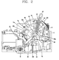
- FIG. 2 is a cross-sectional view illustrating a circuit breaker according to the present disclosure
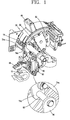
- FIG. 3 is a perspective view illustrating a switching mechanism in FIG. 2 .
- a circuit breaker may include a stationary contact 10 installed in a fixed manner within a case (C); a movable contact 20 configured to be brought into contact with or separated from the stationary contact 10; and a switching mechanism 130 configured to rotate the movable contact 20 so as to switch a circuit.
- the stationary contact 10 and the movable contact 20 may be brought into contact with each other to form a conduction path so as to receive power from the side of a power source and transfer it to the side of a load, and separated from each other to break the circuit.
- the stationary contact 10 may be installed in a fixed manner within the case (C), and connected to the side of a power source or load.
- the movable contact 20 may be hinge-coupled to the case (C) at one side thereof, and hinge-coupled to a transfer link 90 which will be described later at the other side thereof, and connected to the side of a load or power source.
- a portion hinge-coupled to the case (C) is a movable contact rotation shaft 22.
- the switching mechanism 30 may include a handle 40 provided for a user to perform a switching operation, a tension spring 50 for generating a driving force to allow the movable contact 20 to be brought into contact with or separated from the stationary contact 10, and a link apparatus 160 for transferring a driving force tot eh movable contact 20.
- An end of the handle 40 may be hinge-coupled to an inner portion of the case (C), and the other end thereof may be protruded from the case (C).
- a first spring fastening portion 42 may be provided at one side of the handle 40 separated from a handle rotation shaft (not shown).
- the first spring fastening portion 42 may move around an axis formed between a rocker rotation axis 64 and a second spring fastening portion 68a which will be described later from one side in a direction opposite to the one side.
- the tension spring 50 may be supported by the first spring fastening portion 42 at one end thereof, and supported by the second spring fastening portion 68a which will be described later at the other end thereof.
- the link apparatus 160 may include a latch 62 for performing a trip operation, a rocker 66 for performing the role of a driving member joint with respect to the entire link apparatus 160, and a connecting link 70 for connecting the rocker 66 to a shaft 74 which will be described later, a shaft 74 for performing the role of a driving member joint with respect to the movable contact 20 while at the same time performing the role of a follower member joint with respect to the rocker 66, and a transfer link 90 for connecting the shaft 74 to the movable contact 20.
- the latch 62 may be hinge-coupled to an inner portion of the case (C) at one side thereof, and installed to be engaged with a separate latch holder (H) at the other side thereof.
- the latch 62 may be engaged with the latch holder (H) to perform the role of a fixed supporting position for operating the other constituent elements of the link apparatus 160 when the circuit breaker is in a closing operation (ON) or artificial opening operation (OFF).
- the latch 62 may be released from the latch holder (H) to be rotated when the circuit breaker is in an opening operation (TRIP) due to an accident. Due to this, the latch 62 may perform the role of a link member connected to the other constituent elements of the link apparatus 160.
- the rocker 66 may be rotatably installed in the latch 62 at one side thereof, and hinge-coupled to the connecting link 70 at the other side thereof.
- a second spring fastening portion 68a for supporting the other end of the tension spring 50 may be provided in a pin 68 for hinge-coupling the rocker 66 to the connecting link 70. Due to this, a driving force due to the tension spring 50 is applied to the pin 68, and the rocker 66 may perform the role of a driving member joint with respect to the entire link apparatus 160.
- the second spring fastening portion 68a may be formed on another constituent element such as the rocker 66, or the like.
- the shaft 74 may be rotatably installed in the case (C) at one side thereof, and hinge-coupled to the connecting link 70 at the other side thereof.
- the shaft 74 may be hinge-coupled to the transfer link 90 by an insulating pin 180 which will be described later at separated portions of the one side and the other side thereof.
- the shaft 74 may transfer a driving force received from the rocker 66 through the connecting link 70 to the movable contact 20 through the transfer link 90.
- the shaft 74 may perform the role of a driving member joint with respect to the movable contact 20 while at the same time performing the role of a follower member joint with respect to the rocker 66.
- the connecting link 70 may be hinge-coupled to the other side of the rocker 66 at one side thereof, and hinge-coupled to the other side of the shaft 74 at the other side thereof as described above.
- the transfer link 90 may be hinge-coupled to at separated portions of the one side and the other side of the shaft 74 by an insulating pin 180 which will be described later at one side thereof as described above, and hinge-coupled to the other side of the movable contact 20 at the other side thereof.
- the insulating pin 180 may hinge-couple the shaft 74 to the transfer link 90 as well as insulate the shaft 74 and the transfer link 90 from each other.
- portions hinge-coupled thereto by the insulating pin 180 may be referred to as a shaft connecting port 74c and a transfer link connecting port 90c.
- a shaft connecting port 74c portions hinge-coupled thereto by the insulating pin 180
- a transfer link connecting port 90c portions hinge-coupled thereto by the insulating pin 180
- separated portions of the one side and the other side thereof may be referred to as the shaft connecting port 74c
- one side of the transfer link 90 may be referred to as the transfer link connecting port 90c.
- FIG. 4 is a cross-sectional view illustrating the process of forming an insulating member in FIG. 3
- FIG. 5 is a perspective view illustrating the process of forming a wear resistant member in FIG. 3
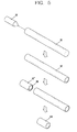
- FIG. 6 is an assembly view illustrating an insulating member and a wear resistant member in FIGS. 4 and 5
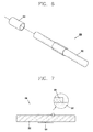
- FIG. 7 is a cross-sectional view subsequent to the assembly of FIG. 6
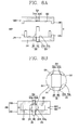
- FIG. 8 is a cross-sectional view illustrating the process of pressing an insulating pin with a press
- FIG. 9 is a cross-sectional view illustrating the insulating pin of FIG. 3 fabricated by the pressure process of FIG. 8
- FIG. 10 is a cross-sectional view in FIG. 9
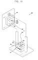
- FIG. 11 is a perspective view illustrating a press in FIG. 8 .
- the insulating pin 180 may include a wear resistant member 184 installed to surround a contact portion between an insulating member 182 formed in a cylindrical rod shape and the shaft connecting port 74c of the insulating member 182.
- the insulating member 182 may be formed of polyethylene, but may be also formed of other materials having an insulating performance.
- the wear resistant member 184 may be formed of stainless steel, but may be also formed of other materials having a wear resistance larger than that of the insulating member 182.
- the insulating pin 180 may be fabricated as follows.
- the insulating member 182 may be formed in a cylindrical rod shape as described above.
- the insulating member 182 may be formed using a drawing process for allowing a raw material (S1) to pass through a drawing die (D1) and then cutting the raw material (S1) as illustrated in FIG. 4 .
- the wear resistant member 184 may be formed in a cylinder shape having a length shorter than that of the insulating member 182, and a length greater than that of a contact portion to the shaft connecting port 74c of the insulating member 182 to surround the circumference of a contact portion to the shaft connecting port 74c of the insulating member 182.
- the wear resistant member 184 may be formed perpendicular to an outer circumferential surface and an inner circumferential surface of the wear resistant member 184 as illustrated in FIGS. 5 through 7 prior to pressing the cross section of both end portions at an initial stage.
- the wear resistant member 184 may have a release resistance strength subsequent to pressure process lower than when the cross section of the end portion is formed perpendicular to the inner circumferential surface.
- the wear resistant member 184 may be formed such that a cylindrically shaped material (S2) is drilled in a length direction by a drill (D2), and the drilled material (S2') is cut by a predetermined length, and a burr (BR) of the cut material (S") is removed as illustrated in FIG. 5 .
- the wear resistant member 184 may be subject to a dimensional deformation problem.
- the wear resistant member 184 may be preferably formed that the cylindrically shaped material (S2) is drilled in a length direction, and the drilled material (S2') is cut by a predetermined length, and a burr (BR) of the cut material (S") is removed as described above.
- the predetermined length is a length shorter than that of the insulating member 182, and greater than that of a contact portion to the shaft connecting port 74c of the insulating member 182 to surround the circumference of a contact portion to the shaft connecting port 74c of the insulating member 182.
- the insulating member 182 and the wear resistant member 184 formed as described above may be formed in such a manner that the insulating member 182 is inserted into an inner side of the wear resistant member 184 as illustrated in FIGS. 6 and 7 .
- the wear resistant member 184 is attached to a contact portion to the shaft connecting port 74c of the insulating member 182.
- At least one end of the wear resistant member 184 may be plastically deformed to burrow into an inner side, namely, toward a central portion thereof from an outer circumferential surface of the insulating member 182 by a pressure process such as a caulking process or the like.
- the wear resistant member 184 may be plastically deformed to allow both end portions to burrow into an inner side from an outer circumferential surface of the insulating member 182 with a pressure process using the press 200 as illustrated in FIGS. 8 and 10 .
- both end portions of the wear resistant member 184 disposed at a contact portion to the shaft connecting port 74c of the insulating member 182 as illustrated in FIG. 7 may be pressed against the press 200 as illustrated in FIG. 8 .
- the press 200 may press both ends of the wear resistant member 184 in an axial direction of the wear resistant member 184 by a predetermined dimension.
- the press 200 may include a die 210 installed in a fixed manner, and a punch 220 installed to face the die 210 so as to move toward the die 210 as illustrated in FIGS. 8 and 11 .
- the die 210 may include a first press surface 212 which is a plane facing in parallel to a second press surface 222 of the punch 220 which will be described later and a first groove 214 formed perpendicular to the first press surface 212.
- the first groove 214 may include a first insertion portion 214b formed in an engraved cylindrical shape in a direction perpendicular to the first press surface 212.
- first groove 214 may include a first chamfer portion 214a inclined to an inner circumferential surface of the first insertion portion 214b and the first press surface 212, respectively.
- the insulating pin 180 in a state that the wear resistant member 184 is disposed at a contact portion to the shaft connecting port 74c of the insulating member 182 may be formed such that an end of the wear resistant member 184 is engaged with the first chamfer portion 214a, and an end of the insulating member 182 protruded from an end of the wear resistant member 184 is inserted into the first insertion portion 214b.
- the insulating pin 180 prior to plastic deformation may be placed perpendicular to the first press surface 212 with respect to the length direction.
- the punch 220 may include a second press surface 222 which is a plane facing in parallel to the first press surface 212 and a second groove 224 formed perpendicular to the second press surface 222 to correspond to the first groove 214.
- the second groove 224 may include a second insertion portion 224b formed in an engraved cylindrical shape in a direction perpendicular to the second press surface 222.
- the second groove 224 may include a second chamfer portion 224a inclined to an inner circumferential surface of the second insertion portion 224b and the second press surface 222 and, respectively.
- the insulating pin 180 prior to plastic deformation placed on the die may be formed such that the other end of the wear resistant member 184 is engaged with the second chamfer portion 224a, and the other end of the insulating member 182 protruded from the other end of the wear resistant member 184 is inserted into the second insertion portion 224b.
- first chamfer portion 214a is formed to be inclined to an inner circumferential surface of the first insertion portion 214b and the second chamfer portion 224a is formed to be inclined to an inner circumferential surface of the second insertion portion 224b.
- the first chamfer portion 214a and the second chamfer portion 224a deform both ends of the wear resistant member 184 while moving along an inclined surface to burrow into the insulating member 182 when both ends of the wear resistant member 184 is pressed.
- the die 210 and the punch 220 may include an excessive compression prevention protrusion (B) configured not to allow the first press surface 212 and the second press surface 222 to get closer more than a predetermined distance when pressing both ends of the wear resistant member 184.
- B excessive compression prevention protrusion
- the excessive compression prevention protrusion (B) may include a first excessive compression prevention protrusion 216 protruded toward the second press surface from the first press surface 212 and a second excessive compression prevention protrusion 226 protruded to face the first excessive compression prevention protrusion 216 from the second press surface 222.
- the sum of a protrusion length from the first press surface 212 of the first excessive compression prevention protrusion 216 and a protrusion length from the second press surface 222 of the second excessive compression prevention protrusion 226 may be formed to be the same as the predetermined distance.
- the predetermined dimension and the predetermined distance may be a value for preventing a bending phenomenon from occurring on an outer circumferential surface of the wear resistant member 184.
- the bending phenomenon refers to a phenomenon a rugged bend are generated on an outer circumferential surface of the wear resistant member 184 when both ends of the wear resistant member 184 is excessively pressed.
- both ends of the wear resistant member 184 pressed by the press 200 provided as described above may be plastically deformed to burrow into an inner side from an outer circumferential surface of the insulating member 182 as illustrated in FIG. 10 .
- the wear resistant member 184 may be installed in a fixed manner at a contact portion to the shaft connecting port 74c of the insulating member 182 not to be released in a length direction of the insulating member 182, namely, in an axial direction of the insulating member 182.
- the present disclosure may not be necessarily limited to this, and there may be various modified examples for a method of fabricating the insulating pin 180.
- the insulating member 182 are formed with a drawing process according to the present embodiment, but may be also formed with a cutting process or the like.
- the cross section of an end portion of the wear resistant member 184 prior to performing a pressure process may be formed perpendicular to an outer circumferential surface and an inner circumferential surface of the wear resistant member 184 according to the present embodiment, but may be also formed with other shapes if it is able to achieve the foregoing objective (when an end portion of the wear resistant member is formed with a pressure process, it is plastically deformed in the form having an excellent release resistance strength).
- an end portion of the wear resistant member 184 may be deformed and fixed to the insulating member 182 according to the present embodiment, but may be also fixed thereto using an adhesive or the like.
- the insulating pin 180 may be formed with a method as illustrated in FIG. 12 .
- FIG. 12 is a cross-sectional view illustrating another embodiment of an insulating pin in FIG. 3 .
- the insulating pin 280 formed with a different method may include a wear resistant member 284 having a protruding portion and an insulating member 282 overlaid on the protruding portion.
- the wear resistant member 284 having the protruding portion may include a shaft connecting port contact portion 284a formed in a cylindrical shape and a protruding portion 284b extended and formed in a length direction of the shaft connecting port contact portion 284a from at least one end portion of the shaft connecting port contact portion 284a.
- the protruding portion 284b may be extended and formed in a length direction of the shaft connecting port contact portion 284a from the center of an end portion of the shaft connecting port contact portion 284a.
- the protruding portion 284b may have a diameter smaller than that of the shaft connecting port contact portion 284a.
- the insulating member 282 overlaid on the protruding portion may be formed in a cylindrical shape having a diameter smaller than that of the shaft connecting port contact portion 284a and a diameter greater than that of the protruding portion 284b.
- a groove portion 282a into which the protruding portion 284b is inserted may be formed at the center of an end portion of the insulating member 282 overlaid on the protruding portion.
- the wear resistant member 284 having the protruding portion and the insulating member 282 overlaid on the protruding portion may be fastened in such a manner that the protruding portion 284b is inserted into the groove portion 282a.
- the wear resistant member 284 having the protruding portion and the insulating member 282 overlaid on the protruding portion may be fastened by a frictional force due to a surface contact between the protruding portion 284b and the groove portion 282a.
- the wear resistant member 284 having the protruding portion and the insulating member 282 overlaid on the protruding portion may be fastened with a different method.
- the release preventing protrusion may be caught in the release preventing groove. Due to this, the wear resistant member 284 having the protruding portion and the insulating member 282 overlaid on the protruding portion are fastened with each other.
- the press 200 may be formed in such a manner that the first excessive compression prevention protrusion 216 is protruded from the first press surface 212 and the second excessive compression prevention protrusion 226 is protruded from the second press surface 222. Furthermore, the first excessive compression prevention protrusion 216 and the second excessive compression prevention protrusion 226 may be brought into contact with each other during a pressure process not to allow the first press surface 212 and the second press surface 222 to get closer more than a predetermined distance.
- only the first excessive compression prevention protrusion 216 may be formed on the press 200.
- the second press surface 222 may be extended and formed in a flat manner up to a portion corresponding to the first excessive compression prevention protrusion 216.
- the first excessive compression prevention protrusion 216 may be formed in such a manner that a protrusion length from the first press surface 212 is the same as the predetermined distance.
- the first excessive compression prevention protrusion 216 may be brought into contact with second press surface 222, thereby suppressing the first and the second press surface from getting closer more than a predetermined distance.
- the excessive compression prevention protrusion (B) can be omitted as a whole.
- the moving distance of the punch 220 may be controlled not to allow the first press surface 212 and the second press surface 222 to get closer than a predetermined distance.
- first excessive compression prevention protrusion 216 and the second excessive compression prevention protrusion 226 may be formed to be protruded from another portion such as a lateral surface of the die 210, a lateral surface of the 220, or the like.
- first excessive compression prevention protrusion 216 and the second excessive compression prevention protrusion 226 may be formed to be protruded from a portion other than the first press surface 212 and the second press surface 222.
- a pair of the first excessive compression prevention protrusions 216 may be formed to be located at opposite sides to each other by interposing the first groove 214 therebetween, and a pair of the second excessive compression prevention protrusions 226 may be formed to be located at opposite sides to each other by interposing the second groove 224 therebetween to correspond to the pair of the first excessive compression prevention protrusions 216.
- first excessive compression prevention protrusion 216 and the second excessive compression prevention protrusion 226 may be formed in a different shape.
- first excessive compression prevention protrusion 216 and the second excessive compression prevention protrusion 226 may be formed thereon.
- a circuit breaker according to the present disclosure may be formed with a plurality of phases, and a pair of the stationary contact 10 and the movable contact 20 may be provided for each phase.
- the switching mechanism 130 should be formed with a structure capable of switching a plurality of the movable contacts 20.
- the transfer link 90 and the insulating pin 180 may be provided for each phase, and the other constituent elements of the switching mechanism 130 may be provided one by one.
- the shaft arm 74b protruded in a radial direction from the shaft rotation axis 74a may be formed for the shaft 74 for each phase.
- the shaft arm 74b is hinge-coupled to the transfer link 90 by the insulating pin 180.
- the latch 62, the rocker 66, the connecting link 70 and the shaft 74 may constitute a 5-joint link mechanism when the circuit breaker performs an opening operation (TRIP) due to an accident.
- TRIP opening operation
- a link for virtually connecting the latch rotation axis 62a to the shaft rotation axis 74a constitutes a stationary joint, and the latch 62, the rocker 66, the connecting link 70 and the shaft 74 are able to move.
- the latch 62, the rocker 66, the connecting link 70 and the shaft 74 may constitute a 4-joint link mechanism when the circuit breaker performs a closing operation (ON) or artificial opening operation (TRIP).
- the latch 62 may be fixed by the latch holder (H).
- a link for virtually connecting the rocker rotation axis 64 to the shaft rotation axis 74a constitutes a stationary joint, and the rocker 66, the connecting link 70 and the shaft 74 are able to move.
- the 4-joint link mechanism configured with the latch 62, the rocker 66, the connecting link 70 and the shaft 74 is referred to as the 4-joint link mechanism configured with the rocker 66, the connecting link 70 and the shaft 74.
- the shaft 74, the transfer link 90 and the movable contact 20 may constitute a 4-joint link mechanism.
- a link for virtually connecting the shaft 74 to the movable contact 20 constitutes a stationary joint, and the shaft 74, the transfer link 90 and the movable contact 20 are able to move.
- the 4-joint link mechanism configured with the shaft 74, the transfer link 90 and the movable contact 20 may share the shaft 74 with a 5-joint link mechanism configured with the latch 62, the rocker 66, the connecting link 70 and the shaft 74 (or a 4-joint link mechanism configured with the rocker 66, the connecting link 70 and the shaft 74.
- the 4-joint link mechanism configured with the shaft 74, the transfer link 90 and the movable contact 20 may be a link mechanism driven by the 5-joint link mechanism configured with the latch 62, the rocker 66, the connecting link 70 and the shaft 74 (or 4-joint link mechanism configured with the rocker 66, the connecting link 70 and the shaft 74).
- a spring force may be applied to the second spring fastening portion 68a in a left upward direction on the drawing.
- the spring force may rotate the rocker 66 in a clockwise direction on the drawing, and rotate the shaft 74 in a clockwise direction on the drawing, and as a result, it may be operated as a driving force for rotating the movable contact 20 in a counter clockwise direction on the drawing.
- the rocker 66 may be rotated in a clockwise direction on the drawing.
- the connecting link 70 may be engaged with the pin 68 provided with the second spring fastening portion 68a, and moved while being rotated in a counter clockwise direction on the drawing.
- the shaft 74 may be rotated in a clockwise direction on the drawing.
- the transfer link 90 may be engaged with the insulating pin 180, and moved while being rotated in a counter clockwise direction on the drawing.
- the movable contact 20 may be rotated in a counter clockwise direction on the drawing to be brought into contact with the stationary contact 10.
- the circuit breaker may be in a closing operation (ON) state.
- the process of switching a circuit breaker from a closing operation (ON) state to an artificial opening operation (OFF) state is opposite to the process of switching a circuit breaker from an artificial opening operation (OFF) state to a closing operation (ON) state as described above, and the detailed description thereof will be omitted.
- the latch holder (H) When an abnormal current occurs in the closing operation (ON) state, the latch holder (H) may be rotated in a clockwise direction to release the locking of the latch 62.
- the latch 62 may be rotated around the latch rotation axis 62a.
- the spring force that has been applied to the second spring fastening portion 68a in a left upward direction may rotate the latch 62 in a counter clockwise direction, and rotate the shaft 74 in a counter clockwise direction, and thus operated as a driving force for rotating the movable contact 20 in a clockwise direction.
- the latch 62 may be rotated in a counter clockwise direction.
- the rocker 66 is restricted by the rocker rotation axis 64, and thus moved while being rotated in a counter clockwise direction.
- the connecting link 70 is restricted by the pin 68 provided with the second spring fastening portion 68a, and thus moved while being rotated in a counter clockwise direction.
- the shaft 74 may be rotated in a counter clockwise direction.
- the transfer link 90 may be restricted by the insulating pin 180, and thus moved while being rotated in a clockwise direction.
- the movable contact 20 may be rotated in a counter clockwise direction, and thus separated from the stationary contact 10.
- the circuit breaker may be in an opening operation (TRIP) state due to an accident.
- TRIP opening operation
- the opening operation (TRIP) state when compared to FIG. 2 , may be in a state that the handle 40 may be rotated in a counter clockwise direction, and the latch 62 is released from the locking of the latch holder (H) and rotated in a counter clockwise direction.
- the process of rotating the handle 40 in a clockwise direction to engage the latch 62 with the latch holder (H) again so as to switch the circuit breaker to an artificial opening operation (OFF) state as illustrated in FIG. 2 precedes the process of switching the circuit breaker from a opening operation (TRIP) state due to an accident to an closing operation (ON) state.
- the following process is the same as the process of switching the circuit breaker from the artificial opening operation (OFF) state to the closing operation (ON) state, and the description thereof will be omitted to avoid redundant description.
- the insulating pin 180 may hinge-couple and insulate the shaft 74 and the transfer link 90.
- the insulating pin 180 may be hinge-coupled to the shaft connection opening 74c at the wear resistant member 184, and hinge-coupled to the transfer link connection opening 90c at both ends of the insulating member 182 as illustrated in FIG. 3 .
- the insulating pin 180 may transfer a driving force to the transfer link 90 from the shaft 74.
- the insulating pin 180 may be insulated by the insulating member 182, thereby preventing a current applied to the transfer link 90 from the movable contact 20 from flowing to the shaft 74.
- the insulating pin 180 may perform phase-phase insulation to prevent dielectric breakdown from occurring from a particular phase to another phase through the shaft 74.
- the wear resistant member 184 of the insulating pin 180 may be installed between the shaft connection opening 74c and a contact portion to the shaft 74 of the insulating member 182.
- the wear resistant member 184 may protect the insulating member 182 having a hardness lower than that of the shaft 74, thereby preventing the insulating member 182 from being worn by the shaft 74.
- a circuit breaker and a method of fabricating an insulating pin for a switching mechanism thereof may include the movable contact 20 configured to be brought into contact with or separated from the stationary contact 10 and the switching mechanism 130 configured to switch the movable contact 20.
- the switching mechanism 130 may include the shaft 74 rotatably installed therein, the transfer link configured 90 to transfer a driving force from the shaft 74 to the movable contact 20, and the insulating pin 180 configured to hinge-couple the shaft to the transfer link and insulate them from each other.
- the insulating pin 180 may include the insulating member 182 formed in a cylindrical shape, and the wear resistant member 184 formed with a pipe to be attached to a portion brought into contact with the shaft 74 of the insulating member 182.
- At least one end of the wear resistant member 184 may be deformed to burrow into the insulating member, and thus installed to be fixed to the insulating member 182.
- the wear resistant member 184 may be formed of a material such as stainless steel having a wear resistance greater than that of the insulating member 182 formed of an insulating material such as polyethylene.
- the insulating pin 180 may be fabricated by a method of fabricating an insulating pin for a circuit breaker switching mechanism, and the method may include the first step of forming the insulating member 182 in a cylindrical shape, the second step of forming the wear resistant member 184 in a pipe shape capable of surrounding one side of the insulating member 182 which is a contact portion to the shaft 74, the third step of inserting the insulating member 182 into the wear resistant member 184 and disposing the wear resistant member 184 at one side of the insulating member 182, and the fourth step of deforming both ends of the wear resistant member 184 to burrow into the insulating member 182 so as to fix the wear resistant member 184 to one side of the insulating member 182.
- phase-to-phase insulation may be carried out, and the abrasion and damage of the insulating pin 180 due to the shaft 74 may be suppressed.
- it may be possible to solve a contact pressure reduction and contact resistance increase problem between the movable contact 20 and the stationary contact 10 due to the abrasion and damage of the insulating pin 180.
- the cross section of both end portions of the wear resistant member 184 may be formed perpendicular to an inner circumferential surface thereof by drilling a cylindrically shaped material (S2) in a length direction, and cutting the drilled material (S2') by a predetermined length, and removing a burr (BR) of the cut material (S") during the second step.
- an end portion of the wear resistant member 184 may be deformed to have an excellent release resistance strength during the fourth step.
- both end portions of the wear resistant member 184 may be deformed to burrow into the insulating member 182 by the press 200 capable of pressing both end portion edges of the wear resistant member 184 in an axial direction of the wear resistant member 184 during the fourth step.
- the wear resistant member 184 may be easily fixed to the insulating member 182.
- the press 200 may include the die 210 installed in a fixed manner; and the punch 220 configured to face the die 210, and installed to move toward the die 210.
- At least one of the die 210 and the punch 220 may include an excessive compression prevention protrusion (B) protruded toward the other one thereof.
- the excessive compression prevention protrusion (B) may prevent the die 210 and the punch 220 from getting closer more than a predetermined distance, thereby suppressing the bending phenomenon from occurring on an outer circumferential surface of the wear resistant member 184.
Landscapes
- Engineering & Computer Science (AREA)
- Manufacturing & Machinery (AREA)
- Breakers (AREA)
- Circuit Breakers (AREA)
- Connector Housings Or Holding Contact Members (AREA)
Applications Claiming Priority (2)
| Application Number | Priority Date | Filing Date | Title |
|---|---|---|---|
| KR20130124176A KR101494792B1 (ko) | 2013-10-17 | 2013-10-17 | 배선용 차단기 |
| KR1020130129523A KR101513206B1 (ko) | 2013-10-29 | 2013-10-29 | 배선용 차단기 개폐기구용 핀 제조방법 및 이를 위한 프레스 |
Publications (3)
| Publication Number | Publication Date |
|---|---|
| EP2871653A2 true EP2871653A2 (de) | 2015-05-13 |
| EP2871653A3 EP2871653A3 (de) | 2015-08-26 |
| EP2871653B1 EP2871653B1 (de) | 2017-04-26 |
Family
ID=51225430
Family Applications (1)
| Application Number | Title | Priority Date | Filing Date |
|---|---|---|---|
| EP14178960.2A Active EP2871653B1 (de) | 2013-10-17 | 2014-07-29 | Schutzschalter |
Country Status (7)
| Country | Link |
|---|---|
| US (1) | US9425004B2 (de) |
| EP (1) | EP2871653B1 (de) |
| JP (1) | JP6018144B2 (de) |
| CN (1) | CN104576234B (de) |
| BR (1) | BR102014021527B1 (de) |
| ES (1) | ES2632918T3 (de) |
| IN (1) | IN2014DE02810A (de) |
Families Citing this family (4)
| Publication number | Priority date | Publication date | Assignee | Title |
|---|---|---|---|---|
| KR101447042B1 (ko) * | 2013-11-19 | 2014-10-06 | 엘에스산전 주식회사 | 투입하중증가수단을 구비한 배선용 차단기 |
| KR101810472B1 (ko) | 2016-07-22 | 2017-12-19 | 엘에스산전 주식회사 | 배선용 차단기의 메커니즘 연결 구조 |
| USD906621S1 (en) * | 2017-02-21 | 2020-12-29 | Evoqua Water Technologies Llc | Hollow chain link pin |
| CN108511292B (zh) * | 2017-02-24 | 2019-12-31 | 上海良信电器股份有限公司 | 电动操作装置的挂锁机构 |
Family Cites Families (18)
| Publication number | Priority date | Publication date | Assignee | Title |
|---|---|---|---|---|
| JPS62109406A (ja) | 1985-11-07 | 1987-05-20 | Nec Corp | 発振回路 |
| DE3544666A1 (de) * | 1985-12-13 | 1987-06-19 | Siemens Ag | Hebelanordnung zur uebertragung begrenzter schwenkbewegungen |
| JPS62109406U (de) * | 1985-12-26 | 1987-07-13 | ||
| KR920002690B1 (ko) | 1989-06-30 | 1992-03-31 | 삼성전자 주식회사 | 전력선 반송시 신호변환장치 |
| DE4416090C1 (de) * | 1994-04-20 | 1995-06-14 | Siemens Ag | Lageranordnung für eine Schaltwelle |
| JP3477887B2 (ja) * | 1995-02-28 | 2003-12-10 | 富士電機ホールディングス株式会社 | 開閉器の操作機構 |
| JPH08234561A (ja) | 1995-02-28 | 1996-09-13 | Bridgestone Corp | マグネットローラ |
| JPH10199376A (ja) | 1997-01-09 | 1998-07-31 | Nissin Electric Co Ltd | 断路器の電動操作器 |
| DE20103230U1 (de) * | 2001-02-16 | 2002-06-20 | Siemens AG, 80333 München | Niederspannungs-Leistungsschalter mit einer Lageranordnung für die Schaltwelle |
| KR100512263B1 (ko) | 2003-03-06 | 2005-09-02 | 엘에스산전 주식회사 | 배선용 차단기 |
| EP1494254B1 (de) | 2003-07-02 | 2006-04-19 | Abb Research Ltd. | Kraftübertragungselement, Verfahren zu dessen Herstellung und Vorrichtung zur Durchführung des Verfahrens |
| JP4601487B2 (ja) * | 2005-05-02 | 2010-12-22 | 三菱電機株式会社 | ガス絶縁開閉機器 |
| US7115830B1 (en) * | 2005-06-08 | 2006-10-03 | Eaton Corporation | Redundant pivot trip latch |
| KR100771922B1 (ko) | 2006-10-17 | 2007-11-01 | 엘에스산전 주식회사 | 기중 차단기 |
| JP5017033B2 (ja) | 2007-09-19 | 2012-09-05 | 株式会社リコー | 現像装置及び画像形成装置 |
| KR101052645B1 (ko) | 2009-10-23 | 2011-07-28 | 엘에스산전 주식회사 | 아크 차폐장치를 갖는 배선용차단기 |
| KR101079012B1 (ko) | 2010-01-20 | 2011-11-01 | 엘에스산전 주식회사 | 한류형 배선용 차단기 |
| KR101677998B1 (ko) * | 2010-12-16 | 2016-11-22 | 엘에스산전 주식회사 | 배선용차단기의 샤프트 어셈블리 |
-
2014
- 2014-07-29 EP EP14178960.2A patent/EP2871653B1/de active Active
- 2014-07-29 ES ES14178960.2T patent/ES2632918T3/es active Active
- 2014-07-31 US US14/448,804 patent/US9425004B2/en not_active Expired - Fee Related
- 2014-08-28 JP JP2014173751A patent/JP6018144B2/ja not_active Expired - Fee Related
- 2014-08-29 BR BR102014021527-1A patent/BR102014021527B1/pt active IP Right Grant
- 2014-10-01 IN IN2810DE2014 patent/IN2014DE02810A/en unknown
- 2014-10-17 CN CN201410555581.5A patent/CN104576234B/zh active Active
Non-Patent Citations (1)
| Title |
|---|
| None |
Also Published As
| Publication number | Publication date |
|---|---|
| US20150107981A1 (en) | 2015-04-23 |
| JP6018144B2 (ja) | 2016-11-02 |
| US9425004B2 (en) | 2016-08-23 |
| EP2871653A3 (de) | 2015-08-26 |
| BR102014021527A2 (pt) | 2015-09-15 |
| EP2871653B1 (de) | 2017-04-26 |
| ES2632918T3 (es) | 2017-09-18 |
| CN104576234B (zh) | 2017-04-12 |
| BR102014021527B1 (pt) | 2022-02-01 |
| CN104576234A (zh) | 2015-04-29 |
| JP2015079743A (ja) | 2015-04-23 |
| IN2014DE02810A (de) | 2015-06-26 |
Similar Documents
| Publication | Publication Date | Title |
|---|---|---|
| EP2871653B1 (de) | Schutzschalter | |
| JP5753465B2 (ja) | コネクタ係合体 | |
| EP2949429B1 (de) | Crimpwerkzeug und crimpmatrize | |
| EP2398120A1 (de) | Kontakt-einrichtung | |
| EP2442338B1 (de) | Kontakt für Vakuumunterbrecher | |
| JP2011501354A (ja) | 電気的接続端子 | |
| US9413129B2 (en) | Locator and wire stop device, hand operated crimping tool, and system | |
| EP2768005B1 (de) | Bewegliches und rotierendes kontaktmodul mit doppeltem haltepunkt | |
| EP1914768A1 (de) | Bewegliche Kontaktanordnung für Luftleistungsschalter und Verbindungsverfahren für flexiblen Leiter dafür | |
| US10199188B2 (en) | Gas circuit breaker | |
| EP1547208B1 (de) | Krimpwerkzeug zum krimpen von anschluss- und buchsenkontakten | |
| KR101513206B1 (ko) | 배선용 차단기 개폐기구용 핀 제조방법 및 이를 위한 프레스 | |
| WO2016081081A1 (en) | Vacuum switching apparatus, and contact assembly and method of securing an electrical contact to an electrode therefor | |
| CN104599868B (zh) | 具有活动地布置的销针的电的触头 | |
| JP2008097903A (ja) | 接続端子 | |
| JP7391245B2 (ja) | ガス絶縁開閉装置 | |
| KR101494792B1 (ko) | 배선용 차단기 | |
| CN104303252B (zh) | 电路断路器 | |
| CN218351368U (zh) | 用于断路器的超程调整组件和断路器 | |
| JP4816241B2 (ja) | 回路遮断器 | |
| CN112863954B (zh) | 一种具备三合一复合弹簧结构的断路器 | |
| CN115210841B (zh) | 一种用于隔离开关的平衡弹簧组件 | |
| KR20100031017A (ko) | 가스절연 차단기의 가동자 구동장치 | |
| KR20180071639A (ko) | 회로차단기의 투입스프링 차징 장치 | |
| CN107680886B (zh) | 用于断路器的基于连杆的断开止动设备及方法 |
Legal Events
| Date | Code | Title | Description |
|---|---|---|---|
| PUAI | Public reference made under article 153(3) epc to a published international application that has entered the european phase |
Free format text: ORIGINAL CODE: 0009012 |
|
| 17P | Request for examination filed |
Effective date: 20140729 |
|
| AK | Designated contracting states |
Kind code of ref document: A2 Designated state(s): AL AT BE BG CH CY CZ DE DK EE ES FI FR GB GR HR HU IE IS IT LI LT LU LV MC MK MT NL NO PL PT RO RS SE SI SK SM TR |
|
| AX | Request for extension of the european patent |
Extension state: BA ME |
|
| PUAL | Search report despatched |
Free format text: ORIGINAL CODE: 0009013 |
|
| AK | Designated contracting states |
Kind code of ref document: A3 Designated state(s): AL AT BE BG CH CY CZ DE DK EE ES FI FR GB GR HR HU IE IS IT LI LT LU LV MC MK MT NL NO PL PT RO RS SE SI SK SM TR |
|
| AX | Request for extension of the european patent |
Extension state: BA ME |
|
| RIC1 | Information provided on ipc code assigned before grant |
Ipc: H01H 3/46 20060101AFI20150723BHEP Ipc: H01H 71/52 20060101ALN20150723BHEP Ipc: H01H 1/22 20060101ALN20150723BHEP Ipc: H01H 71/10 20060101ALI20150723BHEP |
|
| R17P | Request for examination filed (corrected) |
Effective date: 20160226 |
|
| RBV | Designated contracting states (corrected) |
Designated state(s): AL AT BE BG CH CY CZ DE DK EE ES FI FR GB GR HR HU IE IS IT LI LT LU LV MC MK MT NL NO PL PT RO RS SE SI SK SM TR |
|
| GRAP | Despatch of communication of intention to grant a patent |
Free format text: ORIGINAL CODE: EPIDOSNIGR1 |
|
| RIC1 | Information provided on ipc code assigned before grant |
Ipc: H01H 1/22 20060101ALN20160720BHEP Ipc: H01H 71/10 20060101ALI20160720BHEP Ipc: H01H 71/52 20060101ALN20160720BHEP Ipc: H01H 3/46 20060101AFI20160720BHEP |
|
| RIC1 | Information provided on ipc code assigned before grant |
Ipc: H01H 1/22 20060101ALN20160801BHEP Ipc: H01H 71/52 20060101AFI20160801BHEP |
|
| INTG | Intention to grant announced |
Effective date: 20160819 |
|
| GRAJ | Information related to disapproval of communication of intention to grant by the applicant or resumption of examination proceedings by the epo deleted |
Free format text: ORIGINAL CODE: EPIDOSDIGR1 |
|
| STAA | Information on the status of an ep patent application or granted ep patent |
Free format text: STATUS: REQUEST FOR EXAMINATION WAS MADE |
|
| REG | Reference to a national code |
Ref country code: DE Ref legal event code: R079 Ref document number: 602014008961 Country of ref document: DE Free format text: PREVIOUS MAIN CLASS: H01H0003460000 Ipc: H01H0071520000 |
|
| INTC | Intention to grant announced (deleted) | ||
| RIC1 | Information provided on ipc code assigned before grant |
Ipc: H01H 1/22 20060101ALN20170102BHEP Ipc: H01H 71/52 20060101AFI20170102BHEP |
|
| GRAP | Despatch of communication of intention to grant a patent |
Free format text: ORIGINAL CODE: EPIDOSNIGR1 |
|
| STAA | Information on the status of an ep patent application or granted ep patent |
Free format text: STATUS: GRANT OF PATENT IS INTENDED |
|
| INTG | Intention to grant announced |
Effective date: 20170214 |
|
| GRAS | Grant fee paid |
Free format text: ORIGINAL CODE: EPIDOSNIGR3 |
|
| GRAA | (expected) grant |
Free format text: ORIGINAL CODE: 0009210 |
|
| STAA | Information on the status of an ep patent application or granted ep patent |
Free format text: STATUS: THE PATENT HAS BEEN GRANTED |
|
| AK | Designated contracting states |
Kind code of ref document: B1 Designated state(s): AL AT BE BG CH CY CZ DE DK EE ES FI FR GB GR HR HU IE IS IT LI LT LU LV MC MK MT NL NO PL PT RO RS SE SI SK SM TR |
|
| REG | Reference to a national code |
Ref country code: GB Ref legal event code: FG4D |
|
| REG | Reference to a national code |
Ref country code: CH Ref legal event code: EP |
|
| REG | Reference to a national code |
Ref country code: AT Ref legal event code: REF Ref document number: 888534 Country of ref document: AT Kind code of ref document: T Effective date: 20170515 |
|
| REG | Reference to a national code |
Ref country code: IE Ref legal event code: FG4D |
|
| REG | Reference to a national code |
Ref country code: DE Ref legal event code: R096 Ref document number: 602014008961 Country of ref document: DE |
|
| REG | Reference to a national code |
Ref country code: FR Ref legal event code: PLFP Year of fee payment: 4 |
|
| REG | Reference to a national code |
Ref country code: NL Ref legal event code: MP Effective date: 20170426 |
|
| REG | Reference to a national code |
Ref country code: LT Ref legal event code: MG4D |
|
| REG | Reference to a national code |
Ref country code: AT Ref legal event code: MK05 Ref document number: 888534 Country of ref document: AT Kind code of ref document: T Effective date: 20170426 |
|
| REG | Reference to a national code |
Ref country code: ES Ref legal event code: FG2A Ref document number: 2632918 Country of ref document: ES Kind code of ref document: T3 Effective date: 20170918 |
|
| PG25 | Lapsed in a contracting state [announced via postgrant information from national office to epo] |
Ref country code: NL Free format text: LAPSE BECAUSE OF FAILURE TO SUBMIT A TRANSLATION OF THE DESCRIPTION OR TO PAY THE FEE WITHIN THE PRESCRIBED TIME-LIMIT Effective date: 20170426 |
|
| PG25 | Lapsed in a contracting state [announced via postgrant information from national office to epo] |
Ref country code: FI Free format text: LAPSE BECAUSE OF FAILURE TO SUBMIT A TRANSLATION OF THE DESCRIPTION OR TO PAY THE FEE WITHIN THE PRESCRIBED TIME-LIMIT Effective date: 20170426 Ref country code: NO Free format text: LAPSE BECAUSE OF FAILURE TO SUBMIT A TRANSLATION OF THE DESCRIPTION OR TO PAY THE FEE WITHIN THE PRESCRIBED TIME-LIMIT Effective date: 20170726 Ref country code: LT Free format text: LAPSE BECAUSE OF FAILURE TO SUBMIT A TRANSLATION OF THE DESCRIPTION OR TO PAY THE FEE WITHIN THE PRESCRIBED TIME-LIMIT Effective date: 20170426 Ref country code: HR Free format text: LAPSE BECAUSE OF FAILURE TO SUBMIT A TRANSLATION OF THE DESCRIPTION OR TO PAY THE FEE WITHIN THE PRESCRIBED TIME-LIMIT Effective date: 20170426 Ref country code: AT Free format text: LAPSE BECAUSE OF FAILURE TO SUBMIT A TRANSLATION OF THE DESCRIPTION OR TO PAY THE FEE WITHIN THE PRESCRIBED TIME-LIMIT Effective date: 20170426 Ref country code: GR Free format text: LAPSE BECAUSE OF FAILURE TO SUBMIT A TRANSLATION OF THE DESCRIPTION OR TO PAY THE FEE WITHIN THE PRESCRIBED TIME-LIMIT Effective date: 20170727 |
|
| PG25 | Lapsed in a contracting state [announced via postgrant information from national office to epo] |
Ref country code: PL Free format text: LAPSE BECAUSE OF FAILURE TO SUBMIT A TRANSLATION OF THE DESCRIPTION OR TO PAY THE FEE WITHIN THE PRESCRIBED TIME-LIMIT Effective date: 20170426 Ref country code: IS Free format text: LAPSE BECAUSE OF FAILURE TO SUBMIT A TRANSLATION OF THE DESCRIPTION OR TO PAY THE FEE WITHIN THE PRESCRIBED TIME-LIMIT Effective date: 20170826 Ref country code: BG Free format text: LAPSE BECAUSE OF FAILURE TO SUBMIT A TRANSLATION OF THE DESCRIPTION OR TO PAY THE FEE WITHIN THE PRESCRIBED TIME-LIMIT Effective date: 20170726 Ref country code: RS Free format text: LAPSE BECAUSE OF FAILURE TO SUBMIT A TRANSLATION OF THE DESCRIPTION OR TO PAY THE FEE WITHIN THE PRESCRIBED TIME-LIMIT Effective date: 20170426 Ref country code: LV Free format text: LAPSE BECAUSE OF FAILURE TO SUBMIT A TRANSLATION OF THE DESCRIPTION OR TO PAY THE FEE WITHIN THE PRESCRIBED TIME-LIMIT Effective date: 20170426 Ref country code: SE Free format text: LAPSE BECAUSE OF FAILURE TO SUBMIT A TRANSLATION OF THE DESCRIPTION OR TO PAY THE FEE WITHIN THE PRESCRIBED TIME-LIMIT Effective date: 20170426 |
|
| REG | Reference to a national code |
Ref country code: DE Ref legal event code: R097 Ref document number: 602014008961 Country of ref document: DE |
|
| PG25 | Lapsed in a contracting state [announced via postgrant information from national office to epo] |
Ref country code: SK Free format text: LAPSE BECAUSE OF FAILURE TO SUBMIT A TRANSLATION OF THE DESCRIPTION OR TO PAY THE FEE WITHIN THE PRESCRIBED TIME-LIMIT Effective date: 20170426 Ref country code: CZ Free format text: LAPSE BECAUSE OF FAILURE TO SUBMIT A TRANSLATION OF THE DESCRIPTION OR TO PAY THE FEE WITHIN THE PRESCRIBED TIME-LIMIT Effective date: 20170426 Ref country code: EE Free format text: LAPSE BECAUSE OF FAILURE TO SUBMIT A TRANSLATION OF THE DESCRIPTION OR TO PAY THE FEE WITHIN THE PRESCRIBED TIME-LIMIT Effective date: 20170426 Ref country code: RO Free format text: LAPSE BECAUSE OF FAILURE TO SUBMIT A TRANSLATION OF THE DESCRIPTION OR TO PAY THE FEE WITHIN THE PRESCRIBED TIME-LIMIT Effective date: 20170426 Ref country code: DK Free format text: LAPSE BECAUSE OF FAILURE TO SUBMIT A TRANSLATION OF THE DESCRIPTION OR TO PAY THE FEE WITHIN THE PRESCRIBED TIME-LIMIT Effective date: 20170426 |
|
| PG25 | Lapsed in a contracting state [announced via postgrant information from national office to epo] |
Ref country code: SM Free format text: LAPSE BECAUSE OF FAILURE TO SUBMIT A TRANSLATION OF THE DESCRIPTION OR TO PAY THE FEE WITHIN THE PRESCRIBED TIME-LIMIT Effective date: 20170426 |
|
| REG | Reference to a national code |
Ref country code: CH Ref legal event code: PL |
|
| PLBE | No opposition filed within time limit |
Free format text: ORIGINAL CODE: 0009261 |
|
| STAA | Information on the status of an ep patent application or granted ep patent |
Free format text: STATUS: NO OPPOSITION FILED WITHIN TIME LIMIT |
|
| 26N | No opposition filed |
Effective date: 20180129 |
|
| PG25 | Lapsed in a contracting state [announced via postgrant information from national office to epo] |
Ref country code: CH Free format text: LAPSE BECAUSE OF NON-PAYMENT OF DUE FEES Effective date: 20170731 Ref country code: LI Free format text: LAPSE BECAUSE OF NON-PAYMENT OF DUE FEES Effective date: 20170731 |
|
| REG | Reference to a national code |
Ref country code: IE Ref legal event code: MM4A |
|
| PG25 | Lapsed in a contracting state [announced via postgrant information from national office to epo] |
Ref country code: SI Free format text: LAPSE BECAUSE OF FAILURE TO SUBMIT A TRANSLATION OF THE DESCRIPTION OR TO PAY THE FEE WITHIN THE PRESCRIBED TIME-LIMIT Effective date: 20170426 |
|
| REG | Reference to a national code |
Ref country code: FR Ref legal event code: PLFP Year of fee payment: 5 |
|
| REG | Reference to a national code |
Ref country code: BE Ref legal event code: MM Effective date: 20170731 |
|
| PG25 | Lapsed in a contracting state [announced via postgrant information from national office to epo] |
Ref country code: LU Free format text: LAPSE BECAUSE OF NON-PAYMENT OF DUE FEES Effective date: 20170729 |
|
| PG25 | Lapsed in a contracting state [announced via postgrant information from national office to epo] |
Ref country code: IE Free format text: LAPSE BECAUSE OF NON-PAYMENT OF DUE FEES Effective date: 20170729 |
|
| PG25 | Lapsed in a contracting state [announced via postgrant information from national office to epo] |
Ref country code: BE Free format text: LAPSE BECAUSE OF NON-PAYMENT OF DUE FEES Effective date: 20170731 |
|
| PG25 | Lapsed in a contracting state [announced via postgrant information from national office to epo] |
Ref country code: MT Free format text: LAPSE BECAUSE OF NON-PAYMENT OF DUE FEES Effective date: 20170729 |
|
| PG25 | Lapsed in a contracting state [announced via postgrant information from national office to epo] |
Ref country code: MC Free format text: LAPSE BECAUSE OF FAILURE TO SUBMIT A TRANSLATION OF THE DESCRIPTION OR TO PAY THE FEE WITHIN THE PRESCRIBED TIME-LIMIT Effective date: 20170426 Ref country code: HU Free format text: LAPSE BECAUSE OF FAILURE TO SUBMIT A TRANSLATION OF THE DESCRIPTION OR TO PAY THE FEE WITHIN THE PRESCRIBED TIME-LIMIT; INVALID AB INITIO Effective date: 20140729 |
|
| PG25 | Lapsed in a contracting state [announced via postgrant information from national office to epo] |
Ref country code: CY Free format text: LAPSE BECAUSE OF FAILURE TO SUBMIT A TRANSLATION OF THE DESCRIPTION OR TO PAY THE FEE WITHIN THE PRESCRIBED TIME-LIMIT Effective date: 20170426 |
|
| PG25 | Lapsed in a contracting state [announced via postgrant information from national office to epo] |
Ref country code: MK Free format text: LAPSE BECAUSE OF FAILURE TO SUBMIT A TRANSLATION OF THE DESCRIPTION OR TO PAY THE FEE WITHIN THE PRESCRIBED TIME-LIMIT Effective date: 20170426 |
|
| PG25 | Lapsed in a contracting state [announced via postgrant information from national office to epo] |
Ref country code: TR Free format text: LAPSE BECAUSE OF FAILURE TO SUBMIT A TRANSLATION OF THE DESCRIPTION OR TO PAY THE FEE WITHIN THE PRESCRIBED TIME-LIMIT Effective date: 20170426 |
|
| PG25 | Lapsed in a contracting state [announced via postgrant information from national office to epo] |
Ref country code: PT Free format text: LAPSE BECAUSE OF FAILURE TO SUBMIT A TRANSLATION OF THE DESCRIPTION OR TO PAY THE FEE WITHIN THE PRESCRIBED TIME-LIMIT Effective date: 20170426 |
|
| PG25 | Lapsed in a contracting state [announced via postgrant information from national office to epo] |
Ref country code: AL Free format text: LAPSE BECAUSE OF FAILURE TO SUBMIT A TRANSLATION OF THE DESCRIPTION OR TO PAY THE FEE WITHIN THE PRESCRIBED TIME-LIMIT Effective date: 20170426 |
|
| P01 | Opt-out of the competence of the unified patent court (upc) registered |
Effective date: 20230625 |
|
| PGFP | Annual fee paid to national office [announced via postgrant information from national office to epo] |
Ref country code: GB Payment date: 20250610 Year of fee payment: 12 |
|
| PGFP | Annual fee paid to national office [announced via postgrant information from national office to epo] |
Ref country code: FR Payment date: 20250611 Year of fee payment: 12 |
|
| PGFP | Annual fee paid to national office [announced via postgrant information from national office to epo] |
Ref country code: ES Payment date: 20250822 Year of fee payment: 12 |
|
| PGFP | Annual fee paid to national office [announced via postgrant information from national office to epo] |
Ref country code: DE Payment date: 20250609 Year of fee payment: 12 |
|
| PGFP | Annual fee paid to national office [announced via postgrant information from national office to epo] |
Ref country code: IT Payment date: 20250610 Year of fee payment: 12 |