EP2866260A2 - Solid-state imaging apparatus, method for manufacturing the same, and imaging system - Google Patents
Solid-state imaging apparatus, method for manufacturing the same, and imaging system Download PDFInfo
- Publication number
- EP2866260A2 EP2866260A2 EP20140184612 EP14184612A EP2866260A2 EP 2866260 A2 EP2866260 A2 EP 2866260A2 EP 20140184612 EP20140184612 EP 20140184612 EP 14184612 A EP14184612 A EP 14184612A EP 2866260 A2 EP2866260 A2 EP 2866260A2
- Authority
- EP
- European Patent Office
- Prior art keywords
- semiconductor region
- region
- conductivity type
- type semiconductor
- impurity concentration
- Prior art date
- Legal status (The legal status is an assumption and is not a legal conclusion. Google has not performed a legal analysis and makes no representation as to the accuracy of the status listed.)
- Granted
Links
- 238000000034 method Methods 0.000 title claims abstract description 49
- 238000003384 imaging method Methods 0.000 title claims abstract description 36
- 238000004519 manufacturing process Methods 0.000 title claims description 7
- 239000004065 semiconductor Substances 0.000 claims abstract description 237
- 239000012535 impurity Substances 0.000 claims abstract description 80
- 238000009826 distribution Methods 0.000 claims abstract description 31
- 239000000758 substrate Substances 0.000 claims abstract description 29
- 238000005468 ion implantation Methods 0.000 claims abstract description 26
- 230000007423 decrease Effects 0.000 claims abstract description 9
- 238000006243 chemical reaction Methods 0.000 claims description 23
- 230000002093 peripheral effect Effects 0.000 claims description 8
- 238000002513 implantation Methods 0.000 claims description 3
- 238000005036 potential barrier Methods 0.000 description 7
- 238000009825 accumulation Methods 0.000 description 5
- 230000015572 biosynthetic process Effects 0.000 description 3
- 229920002120 photoresistant polymer Polymers 0.000 description 3
- 230000008569 process Effects 0.000 description 3
- OAICVXFJPJFONN-UHFFFAOYSA-N Phosphorus Chemical compound [P] OAICVXFJPJFONN-UHFFFAOYSA-N 0.000 description 2
- 230000008859 change Effects 0.000 description 2
- 230000007547 defect Effects 0.000 description 2
- 238000009792 diffusion process Methods 0.000 description 2
- 239000002019 doping agent Substances 0.000 description 2
- 238000002955 isolation Methods 0.000 description 2
- 230000003071 parasitic effect Effects 0.000 description 2
- 229910052698 phosphorus Inorganic materials 0.000 description 2
- 239000011574 phosphorus Substances 0.000 description 2
- 239000012808 vapor phase Substances 0.000 description 2
- ZOXJGFHDIHLPTG-UHFFFAOYSA-N Boron Chemical compound [B] ZOXJGFHDIHLPTG-UHFFFAOYSA-N 0.000 description 1
- 102000004129 N-Type Calcium Channels Human genes 0.000 description 1
- 108090000699 N-Type Calcium Channels Proteins 0.000 description 1
- 229910052785 arsenic Inorganic materials 0.000 description 1
- RQNWIZPPADIBDY-UHFFFAOYSA-N arsenic atom Chemical compound [As] RQNWIZPPADIBDY-UHFFFAOYSA-N 0.000 description 1
- 229910052796 boron Inorganic materials 0.000 description 1
- 239000013078 crystal Substances 0.000 description 1
- 230000003247 decreasing effect Effects 0.000 description 1
- 230000000694 effects Effects 0.000 description 1
- 238000012986 modification Methods 0.000 description 1
- 230000004048 modification Effects 0.000 description 1
- 230000035945 sensitivity Effects 0.000 description 1
- 229910052710 silicon Inorganic materials 0.000 description 1
- 239000010703 silicon Substances 0.000 description 1
- 230000000087 stabilizing effect Effects 0.000 description 1
Images


Classifications
-
- H—ELECTRICITY
- H04—ELECTRIC COMMUNICATION TECHNIQUE
- H04N—PICTORIAL COMMUNICATION, e.g. TELEVISION
- H04N23/00—Cameras or camera modules comprising electronic image sensors; Control thereof
- H04N23/10—Cameras or camera modules comprising electronic image sensors; Control thereof for generating image signals from different wavelengths
- H04N23/11—Cameras or camera modules comprising electronic image sensors; Control thereof for generating image signals from different wavelengths for generating image signals from visible and infrared light wavelengths
-
- H—ELECTRICITY
- H04—ELECTRIC COMMUNICATION TECHNIQUE
- H04N—PICTORIAL COMMUNICATION, e.g. TELEVISION
- H04N23/00—Cameras or camera modules comprising electronic image sensors; Control thereof
- H04N23/60—Control of cameras or camera modules
- H04N23/63—Control of cameras or camera modules by using electronic viewfinders
-
- H—ELECTRICITY
- H04—ELECTRIC COMMUNICATION TECHNIQUE
- H04N—PICTORIAL COMMUNICATION, e.g. TELEVISION
- H04N25/00—Circuitry of solid-state image sensors [SSIS]; Control thereof
- H04N25/70—SSIS architectures; Circuits associated therewith
- H04N25/76—Addressed sensors, e.g. MOS or CMOS sensors
-
- H—ELECTRICITY
- H04—ELECTRIC COMMUNICATION TECHNIQUE
- H04N—PICTORIAL COMMUNICATION, e.g. TELEVISION
- H04N5/00—Details of television systems
- H04N5/222—Studio circuitry; Studio devices; Studio equipment
- H04N5/262—Studio circuits, e.g. for mixing, switching-over, change of character of image, other special effects ; Cameras specially adapted for the electronic generation of special effects
- H04N5/265—Mixing
-
- H—ELECTRICITY
- H10—SEMICONDUCTOR DEVICES; ELECTRIC SOLID-STATE DEVICES NOT OTHERWISE PROVIDED FOR
- H10F—INORGANIC SEMICONDUCTOR DEVICES SENSITIVE TO INFRARED RADIATION, LIGHT, ELECTROMAGNETIC RADIATION OF SHORTER WAVELENGTH OR CORPUSCULAR RADIATION
- H10F39/00—Integrated devices, or assemblies of multiple devices, comprising at least one element covered by group H10F30/00, e.g. radiation detectors comprising photodiode arrays
- H10F39/011—Manufacture or treatment of image sensors covered by group H10F39/12
- H10F39/014—Manufacture or treatment of image sensors covered by group H10F39/12 of CMOS image sensors
-
- H—ELECTRICITY
- H10—SEMICONDUCTOR DEVICES; ELECTRIC SOLID-STATE DEVICES NOT OTHERWISE PROVIDED FOR
- H10F—INORGANIC SEMICONDUCTOR DEVICES SENSITIVE TO INFRARED RADIATION, LIGHT, ELECTROMAGNETIC RADIATION OF SHORTER WAVELENGTH OR CORPUSCULAR RADIATION
- H10F39/00—Integrated devices, or assemblies of multiple devices, comprising at least one element covered by group H10F30/00, e.g. radiation detectors comprising photodiode arrays
- H10F39/10—Integrated devices
- H10F39/12—Image sensors
- H10F39/18—Complementary metal-oxide-semiconductor [CMOS] image sensors; Photodiode array image sensors
-
- H—ELECTRICITY
- H10—SEMICONDUCTOR DEVICES; ELECTRIC SOLID-STATE DEVICES NOT OTHERWISE PROVIDED FOR
- H10F—INORGANIC SEMICONDUCTOR DEVICES SENSITIVE TO INFRARED RADIATION, LIGHT, ELECTROMAGNETIC RADIATION OF SHORTER WAVELENGTH OR CORPUSCULAR RADIATION
- H10F39/00—Integrated devices, or assemblies of multiple devices, comprising at least one element covered by group H10F30/00, e.g. radiation detectors comprising photodiode arrays
- H10F39/10—Integrated devices
- H10F39/12—Image sensors
- H10F39/18—Complementary metal-oxide-semiconductor [CMOS] image sensors; Photodiode array image sensors
- H10F39/182—Colour image sensors
-
- H—ELECTRICITY
- H10—SEMICONDUCTOR DEVICES; ELECTRIC SOLID-STATE DEVICES NOT OTHERWISE PROVIDED FOR
- H10F—INORGANIC SEMICONDUCTOR DEVICES SENSITIVE TO INFRARED RADIATION, LIGHT, ELECTROMAGNETIC RADIATION OF SHORTER WAVELENGTH OR CORPUSCULAR RADIATION
- H10F39/00—Integrated devices, or assemblies of multiple devices, comprising at least one element covered by group H10F30/00, e.g. radiation detectors comprising photodiode arrays
- H10F39/10—Integrated devices
- H10F39/12—Image sensors
- H10F39/18—Complementary metal-oxide-semiconductor [CMOS] image sensors; Photodiode array image sensors
- H10F39/184—Infrared image sensors
-
- H—ELECTRICITY
- H10—SEMICONDUCTOR DEVICES; ELECTRIC SOLID-STATE DEVICES NOT OTHERWISE PROVIDED FOR
- H10F—INORGANIC SEMICONDUCTOR DEVICES SENSITIVE TO INFRARED RADIATION, LIGHT, ELECTROMAGNETIC RADIATION OF SHORTER WAVELENGTH OR CORPUSCULAR RADIATION
- H10F39/00—Integrated devices, or assemblies of multiple devices, comprising at least one element covered by group H10F30/00, e.g. radiation detectors comprising photodiode arrays
- H10F39/80—Constructional details of image sensors
- H10F39/802—Geometry or disposition of elements in pixels, e.g. address-lines or gate electrodes
- H10F39/8027—Geometry of the photosensitive area
-
- H—ELECTRICITY
- H10—SEMICONDUCTOR DEVICES; ELECTRIC SOLID-STATE DEVICES NOT OTHERWISE PROVIDED FOR
- H10F—INORGANIC SEMICONDUCTOR DEVICES SENSITIVE TO INFRARED RADIATION, LIGHT, ELECTROMAGNETIC RADIATION OF SHORTER WAVELENGTH OR CORPUSCULAR RADIATION
- H10F39/00—Integrated devices, or assemblies of multiple devices, comprising at least one element covered by group H10F30/00, e.g. radiation detectors comprising photodiode arrays
- H10F39/80—Constructional details of image sensors
- H10F39/803—Pixels having integrated switching, control, storage or amplification elements
- H10F39/8033—Photosensitive area
Definitions
- the present invention relates to a solid-state imaging apparatus, a method for manufacturing the same, and an imaging system.
- a solid-state imaging apparatus includes a photoelectric conversion portion (pn-junction diode) formed on a substrate and reads out charges generated by light which has been incident on the photoelectric conversion portion.
- Japanese Patent Laid-Open No. 2008-034836 discloses a photoelectric conversion portion which is formed by a p-type epitaxial layer provided on a substrate and an n-type epitaxial layer provided on the p-type epitaxial layer.
- the p-type epitaxial layer is formed such that a p-type impurity concentration decreases from the lower side to the upper side.
- the n-type epitaxial layer is formed such that an n-type impurity concentration increases from the lower side to the upper side. According to a structure described in Japanese Patent Laid-Open No. 2008-034836 , for example, the movement in the horizontal direction of charges generated by photoelectric conversion is suppressed, thereby preventing a crosstalk between pixels.
- the charges generated by photoelectric conversion can move under the influence of a potential distribution which is determined by the impurity concentration distribution of the photoelectric conversion portion.
- a potential distribution which is determined by the impurity concentration distribution of the photoelectric conversion portion.
- Each of the above-described n-type and p-type epitaxial layers is formed by epitaxial growth while adjusting a dopant concentration in an epitaxial growth chamber. It is not easy to accurately control the impurity concentration distribution. Hence, according to a photoelectric conversion portion formed by an epitaxial growth method, it is difficult to improve charge transfer efficiency for reading out the charges generated by photoelectric conversion.
- the present invention is advantageous in improving transfer efficiency of charges generated by photoelectric conversion.
- the present invention in its first aspect provides a solid-state imaging apparatus as specified in claims 1 to 12.
- the present invention in its second aspect provides a method for manufacturing a solid-state imaging apparatus as specified in claims 13 to 15.
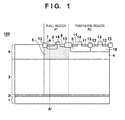
- Fig. 1 is a schematic view for explaining the structure of a solid-state imaging apparatus 100 according to this embodiment.
- the solid-state imaging apparatus 100 includes a pixel region R1 in which pixels are arrayed and a peripheral region R2 in which a unit for exchanging signals between respective pixels is arranged.
- the pixel region R1 is illustrated to include one pixel.
- the unit in the peripheral region R2 includes, for example, at least one of a driving unit configured to drive each pixel, a signal processing unit configured to process a signal read out from each pixel, and an output unit configured to output the signal read out from each.
- the solid-state imaging apparatus 100 includes a p-type (first conductivity type) substrate 1, a p-type semiconductor region 2 provided in the upper portion of the substrate 1, a p-type semiconductor region 3 provided on the p-type semiconductor region 2, and an n-type (second conductivity type) semiconductor region 4 provided on the p-type semiconductor region 3.
- the p-type semiconductor region 2 is a high-concentration impurity region formed by implanting a p-type impurity in the substrate 1.
- the p-type semiconductor region 3 is the first epitaxial layer formed above the substrate 1 (on the p-type semiconductor region 2) by an epitaxial growth method.
- the p-type semiconductor region 3 is formed such that a p-type impurity concentration decreases from the lower side to the upper side.
- the p-type semiconductor region 3 is formed such that the p-type impurity concentration decreases from the side of the substrate 1 to the side of an n-type semiconductor region 6 to be described later.
- the n-type semiconductor region 4 is the second epitaxial layer formed on the p-type semiconductor region 3 by the epitaxial growth method.
- the n-type semiconductor region 4 is provided, while contacting the p-type semiconductor region 3, to be adjacent to a p-type semiconductor region 5 to be described later.
- the solid-state imaging apparatus 100 also includes, in the pixel region R1, the p-type semiconductor region 5 adjacent to the n-type semiconductor region 4.
- the p-type semiconductor region 5 is a p-type well which is formed in a region formed on the p-type semiconductor region 3 (a region formed simultaneously with the n-type semiconductor region 4) by an ion implantation method.
- the p-type semiconductor region 5 may be provided in the upper portion of the p-type semiconductor region 3.
- Respective elements which constitute the pixel are formed in the p-type semiconductor region 5.
- the n-type semiconductor region 6, a p-type semiconductor region 7, an n-type semiconductor region 8, and a gate electrode 14 are illustrated here.
- the gate electrode 14 is formed on an insulating film (not shown) on the p-type semiconductor region 5. Note that the respective elements are isolated by an element isolation portion 13. In addition, the source region and the drain region (both of them are not shown) of each transistor which constitutes the pixel are formed in the p-type semiconductor region 5.
- the n-type semiconductor region 6 forms a pn junction with the p-type semiconductor region 5.
- the p-type semiconductor region 5 and the n-type semiconductor region 6 form a photodiode.
- the p-type semiconductor region 7 is formed such that the n-type semiconductor region 6 serving as the charge accumulation region of the photodiode is isolated from an interface between a semiconductor and the insulating film, thereby reducing a dark current component.
- the photoelectric conversion portion is formed by this structure. Charges are generated in an amount corresponding to the amount of light which has been incident on the photoelectric conversion portion.
- the n-type semiconductor region 8 is also referred to as a floating diffusion region, and its potential is initialized by, for example, a reset transistor (not shown) before reading out the charges generated in the photoelectric conversion portion.
- the charges generated in the photoelectric conversion portion are transferred to the n-type semiconductor region 8 via an n-type channel formed near the surface of the p-type semiconductor region 5 by applying a predetermined voltage to the gate electrode 14. Then, a signal corresponding to the variation amount of the potential in the n-type semiconductor region 8 is read out as a pixel signal.
- One or more PMOS transistors and NMOS transistors which constitute the above-described unit are formed in the peripheral region R2. These transistors are formed in the n-type semiconductor region 4 or in a well formed in the n-type semiconductor region 4. This arrangement reduces noise which occurs when a noise component generated in the peripheral region R2 mixes into the p-type semiconductor region 5 in the pixel region R1.
- the PMOS transistor is formed by an n-type semiconductor region 9 provided in the upper portion of the n-type semiconductor region 4, the gate electrode 14 provided on the insulating film on it, and two p-type semiconductor regions 11 provided in the n-type semiconductor region 9.
- the n-type semiconductor region 9 is an n-type well formed by the ion implantation method.
- Two p-type semiconductor regions 11 are the p-type source region and the p-type drain region of the PMOS transistor.
- the NMOS transistor is formed by an p-type semiconductor region 10 provided in the upper portion of the n-type semiconductor region 4, the gate electrode 14 provided on the insulating film on it, and two n-type semiconductor regions 12 provided in the p-type semiconductor region 10.
- the p-type semiconductor region 10 is a p-type well formed by the ion implantation method.
- Two n-type semiconductor regions 12 are the n-type source region and the n-type drain region of the NMOS transistor.
- a structure in which, for example, a polarity (p type/n type) in each semiconductor region is reversed may be used.
- the substrate 1 and the p-type semiconductor region 3 may be arranged so as to contact each other by omitting the p-type semiconductor region 2.
- the conductivity type of the n-type semiconductor region 4 is not necessarily an n type. In the structure of Fig. 1 , only the conductivity type of the n-type semiconductor region 4 may be changed into the p type or an intrinsic type.
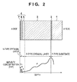
- Fig. 2 is a view for explaining an impurity concentration distribution in the semiconductor regions 1 to 7 along a cut line A - A' in Fig. 1 .
- the impurity concentration distribution is an impurity concentration corresponding to positions, and is typically an impurity concentration represented as a positional function.
- Fig. 2 shows, for example, an impurity concentration corresponding to depths.
- the impurity concentration distribution may simply be referred to as an impurity distribution.
- the p-type semiconductor region 2 is the high-concentration impurity region formed by implanting the p-type impurity in the p-type substrate 1.
- the ion implantation method can form the high-concentration impurity region more easily, and can form a buried high-concentration impurity region as illustrated in the p-type semiconductor region 2. Since a p-type high-concentration impurity region forms a high potential barrier against charges (here, electrons), the p-type semiconductor region 2 prevents the charges generated in the photoelectric conversion portion from leaking to the substrate 1 side.
- the p-type semiconductor region 3 is the epitaxial layer formed on the p-type semiconductor region 2 by the epitaxial growth method.
- the p-type semiconductor region 3 is formed such that the impurity concentration decreases from the lower side (the sides of the substrate 1 and the p-type semiconductor region 2) to the upper side. This can be done by epitaxial growth while adjusting a dopant concentration in an epitaxial growth chamber after loading a substrate in the chamber. According to this impurity concentration distribution, the potential barrier becomes lower from the lower side to the upper side. Therefore, charges generated in the deep position of the substrate are collected efficiently toward the surface (upper side) of the semiconductor region. Furthermore, the epitaxial growth method can form a semiconductor region with a low lattice defect density.
- the semiconductor regions 5 to 7 are respectively the p-type well, an n-type high-concentration impurity region, and the p-type high-concentration impurity region which are formed, by the ion implantation method, in part of the n-type semiconductor region 4 (epitaxial layer) provided on the p-type semiconductor region 3. Note that the n-type semiconductor region 4 (epitaxial layer) may not be formed, and the respective semiconductor regions 5 to 7 may be formed in the upper portion of the p-type semiconductor region 3.
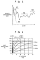
- Fig. 3 is a graph for explaining in detail the impurity concentration distribution of Fig. 2 in the semiconductor regions 5 to 7.
- a solid line indicates the impurity concentration distribution of the p-type impurity, that is, the concentration distribution of an acceptor
- a broken line indicates the impurity concentration distribution of an n-type impurity, that is, the concentration distribution of a donor. Therefore, regions where the impurity concentration indicated by the solid line is higher than that of the broken line form the p-type regions (the semiconductor regions 5 and 7), and a region where the impurity concentration indicated by the broken line is higher than that of the solid line forms the n-type region (the semiconductor region 6).
- the p-type semiconductor region 5 includes regions 301, 302, and 303 in the order from the upper side (the n-type semiconductor region 6 side). An impurity concentration peak of the region 302 is lower than that of the region 303. According to this impurity concentration distribution, charges from the p-type semiconductor region 3 are collected efficiently toward the surface (upper side) of the semiconductor region.
- the formation of the p-type semiconductor region 5 by the ion implantation method is preferably performed by setting an ion implantation condition so as not to generate a potential barrier in a boundary region between the p-type semiconductor region 3 and the p-type semiconductor region 5. Note that ion implantation may be performed a plurality of times under different implantation conditions.
- an impurity concentration peak of the region 301 in the p-type semiconductor region 5 is higher than that of the region 302.
- the region 301 is formed to contact the n-type semiconductor region 6 serving as the charge accumulation region of the photodiode. That is, the region 301 is adjacent to the n-type semiconductor region 6.
- the region 302 is provided under the region 301. This structure narrows the width of a depletion layer in a pn junction formed by the region 301 and the n-type semiconductor region 6, and also reduces a depletion voltage to deplete the n-type semiconductor region 6 serving as the charge accumulation region almost completely. Note that the region 302 is arranged between the region 301 and the p-type semiconductor region 3 because it has the region 303 and the p-type semiconductor region 3 underneath.
- the width of the depletion layer in a pn junction formed by the p-type semiconductor region 5 and the n-type semiconductor region 6 is widened, and the above-described depletion voltage increases as well. Furthermore, if the impurity concentration peak position in the region 301 is deep (on the the p-type semiconductor region 3 side), it may be a potential barrier when collecting charges generated by photoelectric conversion in the n-type semiconductor region 6. If the magnitude relationship of the impurity concentrations between the region 302 and the region 303 is reversed, it may also be the potential barrier. These may bring about a drop in charge transfer efficiency to the n-type semiconductor region 8.
- the respective regions 301 to 303 in the p-type semiconductor region 5 are formed, by the ion implantation method, to form the impurity concentration distribution as illustrated in Fig. 3 .
- the impurity concentration distribution in the p-type semiconductor region 5 is formed by the ion implantation method. More specifically, the impurity concentration distribution which reduces the above-described depletion voltage while efficiently collecting the charges generated by photoelectric conversion from the p-type semiconductor region 3 to the n-type semiconductor region 6 is formed.
- This structure appropriately accumulates the charges generated by photoelectric conversion in the n-type semiconductor region 6 serving as the charge accumulation region, resulting in improved charge transfer efficiency to the n-type semiconductor region 8.
- a semiconductor region with another impurity concentration distribution may be formed by the ion implantation method.
- the thickness of the n-type semiconductor region 4 suffices to be a thickness that can control the impurity concentration distribution at high precision by ion implantation, and fall within in a range of, for example, 1 ⁇ m (inclusive) to 10 ⁇ m (inclusive). Furthermore, the thickness of the p-type semiconductor region 3 suffices to be a thickness suitable for formation by the epitaxial growth method, and fall within a range of, for example, 5 ⁇ m (inclusive) to 500 ⁇ m (inclusive).
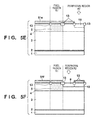
- Fig. 4 shows a light absorptance on a substrate formed by a silicon.
- the abscissa represents the light absorptance and the ordinate represents the thickness of the substrate, and the wavelength ⁇ of light is represented as a parameter.
- the thickness of the p-type semiconductor region 3 is about 50 ⁇ m, charges generated by, for example, red light or an infrared ray are collected efficiently toward the surface (upper side) of the semiconductor region.
- a sensitivity is three to four times as high as in a structure in which a photoelectric conversion portion with a depth of about 3 to 5 ⁇ m is used.
- Figs. 5A to 5F are schematic views showing the respective steps of a method for manufacturing the solid-state imaging apparatus 100.
- a p-type impurity for example, boron
- the p-type semiconductor region 2 can be formed so as to obtain the impurity concentration of about, for example, 1 ⁇ 10 17 to 1 ⁇ 10 18 [cm -3 ]. Note that this step may not be performed.
- the p-type semiconductor region 3 is formed on the p-type semiconductor region 2 by, for example, a vapor phase epitaxial growth method.
- This method advantageously obtains a crystal structure with less lattice defects, reduces noise components, and achieves higher accuracy of the solid-state imaging apparatus 100.
- the p-type semiconductor region 3 is formed such that the impurity concentration decreases from a lower side A (the sides of the substrate 1 and the p-type semiconductor region 2) to an upper side B.
- the impurity concentration distribution falls within a range of, for example, 1 ⁇ 10 15 to 1 ⁇ 10 18 [cm -3 ].
- the impurity concentration distribution need only be formed so as not to generate the potential barrier against the charges (here, the electrons), and may be a gradient having an almost linear curve or may change stepwise.
- a distribution in which the impurity concentration changes in the order of 2 ⁇ 10 17 , 9 ⁇ 10 16 , 4 ⁇ 10 16 , 2 ⁇ 10 16 , and 1 ⁇ 10 16 [cm -3 ] from the lower side A to the upper side B is formed.
- the n-type semiconductor region 4 is formed on the p-type semiconductor region 3 by, for example, the vapor phase epitaxial growth method.
- the n-type semiconductor region 4 is formed so as to obtain the impurity concentration of about, for example, 1 ⁇ 10 14 to 1 ⁇ 10 15 [cm -3 ] by using the n-type impurity such as phosphorus or arsenic.
- the impurity concentration of 5 ⁇ 10 14 [cm -3 ] is obtained by using phosphorus as the n-type impurity.
- an oxide film (not shown) and also the element isolation portion 13 are formed in the n-type semiconductor region 4.
- a photoresist 51d having an opening in the pixel region R1 is formed, and the p-type semiconductor region 5 (p-type well) is formed by implanting the p-type impurity using the ion implantation method.
- the p-type semiconductor region 5 has the impurity concentration distribution as illustrated in Fig. 3 .
- Ion implantation to form the p-type semiconductor region 5 is performed a plurality of times under different implantation conditions.
- the p-type semiconductor region 5 may be formed by a plurality of p-type regions.
- the p-type semiconductor region 5 is preferably formed so as not to generate the potential barrier in the boundary region between the p-type semiconductor region 3 and the p-type semiconductor region 5, as described above.
- a photoresist 51e having an opening in a region of the peripheral region R2 where the NMOS transistor should be formed is formed, and the p-type semiconductor region 10 (p-type well) is formed by implanting the p-type impurity using the ion implantation method.
- the impurity concentration peak in the p-type semiconductor region 5 may be higher than that in the p-type semiconductor region 10, and a voltage (transfer voltage) at the time of resetting the n-type semiconductor region 8 serving as a floating diffusion may be decreased by reducing the above-described depletion voltage.
- a photoresist 51f having an opening in a region of the peripheral region R2 where the PMOS transistor should be formed is formed, and the n-type semiconductor region 9 (n-type well) is formed by implanting the n-type impurity using the ion implantation method.
- the respective elements can be formed using a known semiconductor manufacturing process. More specifically, the respective gate electrodes 14 are formed on a gate insulating film on the semiconductor regions 5, 9, and 10. After formation of the gate electrodes 14, the n-type semiconductor regions 6, 8, and 12, and the p-type semiconductor regions 7 and 11 are additionally formed.
- the photoelectric conversion portion and the respective elements such as the respective MOS transistors are formed, thereby completing the structure as illustrated in Fig. 1 .
- the p-type semiconductor region 5 is formed by the ion implantation method.
- the ion implantation method can adjust the impurity concentration distribution in the p-type semiconductor region 5 at higher precision than the epitaxial growth method. Hence, it is possible to accumulate the charges from the p-type semiconductor region 3 in the n-type semiconductor region 6 serving as the charge accumulation region while efficiently collecting them toward the surface (upper side) of the semiconductor region. As a result, the charge transfer efficiency to the n-type semiconductor region 8 can be improved.
- this embodiment is advantageous in improving charge transfer efficiency.
- this embodiment is advantageous in efficiently accumulating charges generated by light, for example, red light or an infrared ray with a long wavelength that photoelectric conversion can generate in a deep region of a semiconductor substrate, and performing charge transfer.
- the second embodiment will be described with reference to Fig. 6 .
- This embodiment is different from the first embodiment in that an n-type semiconductor region 101 is provided under a p-type semiconductor region 10.
- the impurity concentration in the n-type semiconductor region 101 is higher than that in an n-type semiconductor region 4.
- a pnp parasitic bipolar transistor of the p-type semiconductor region 10, the n-type semiconductor region 4, and a p-type semiconductor region 3 is formed in a peripheral region R2.
- the parasitic bipolar transistor is prevented from being turned on by the n-type semiconductor region 101 serving as a high-concentration impurity region. Therefore, this embodiment is also advantageous in stabilizing the operation of a solid-state imaging apparatus 100 in addition to obtaining the same effects as in the first embodiment.
- the present invention has been described by exemplifying a solid-state imaging apparatus included in an imaging system represented by a camera or the like.
- the concept of the imaging system includes not only apparatuses primarily aiming at shooting but also apparatuses (for example, personal computer and portable terminal) secondarily having a shooting function.
- the imaging system can include the solid-state imaging apparatus according to the present invention exemplified in the above embodiments, and a processor that processes a signal output from the solid-state imaging apparatus.
- the processor can include, for example, an A/D converter, and a processor that processes digital data output from the A/D converter.
- the solid-state imaging apparatus may be used in an imaging system which performs both imaging by a near infrared ray and imaging by visible light.
- This imaging system includes a display unit configured to output a near infrared ray image and a visible light image in a superimposed manner. This arrangement makes it possible to obtain infrared ray information while visually recognizing an object in a normal visible image.
- a solid-state imaging apparatus comprising a first semiconductor region (3) of a first conductivity type provided on a substrate by an epitaxial growth method, a second semiconductor region (5) of the first conductivity type provided on the first semiconductor region, and a third semiconductor region (6) of a second conductivity type provided in the second semiconductor region so as to form a pn junction with the second semiconductor region, wherein the first semiconductor region is formed such that an impurity concentration decreases from a side of the substrate to a side of the third semiconductor region, and an impurity concentration distribution in the second semiconductor region is formed by an ion implantation method.
Landscapes
- Engineering & Computer Science (AREA)
- Multimedia (AREA)
- Signal Processing (AREA)
- Solid State Image Pick-Up Elements (AREA)
- Light Receiving Elements (AREA)
- Transforming Light Signals Into Electric Signals (AREA)
Abstract
Description
- The present invention relates to a solid-state imaging apparatus, a method for manufacturing the same, and an imaging system.
- A solid-state imaging apparatus includes a photoelectric conversion portion (pn-junction diode) formed on a substrate and reads out charges generated by light which has been incident on the photoelectric conversion portion. Japanese Patent Laid-Open No.
2008-034836 2008-034836 - The charges generated by photoelectric conversion can move under the influence of a potential distribution which is determined by the impurity concentration distribution of the photoelectric conversion portion. Each of the above-described n-type and p-type epitaxial layers is formed by epitaxial growth while adjusting a dopant concentration in an epitaxial growth chamber. It is not easy to accurately control the impurity concentration distribution. Hence, according to a photoelectric conversion portion formed by an epitaxial growth method, it is difficult to improve charge transfer efficiency for reading out the charges generated by photoelectric conversion.
- The present invention is advantageous in improving transfer efficiency of charges generated by photoelectric conversion.
- The present invention in its first aspect provides a solid-state imaging apparatus as specified in
claims 1 to 12. - The present invention in its second aspect provides a method for manufacturing a solid-state imaging apparatus as specified in
claims 13 to 15. - Further features of the present invention will become apparent from the following description of exemplary embodiments with reference to the attached drawings.
-
-
Fig. 1 is a view showing an example of the arrangement of a solid-state imaging apparatus; -
Fig. 2 is a view for explaining an impurity concentration distribution in each layer in the solid-state imaging apparatus; -
Fig. 3 is a graph for explaining the impurity concentration distribution of a p-type well in the solid-state imaging apparatus; -
Fig. 4 is a graph for explaining a light absorptance for a semiconductor substrate; -
Figs 5A to 5F are views for explaining an example of a method for manufacturing the solid-state imaging apparatus; and -
Fig. 6 is a view for explaining an example of the arrangement of a solid-state imaging apparatus. - The first embodiment will be described with reference to
Fig. 1 to Figs. 5A to 5F .Fig. 1 is a schematic view for explaining the structure of a solid-state imaging apparatus 100 according to this embodiment. The solid-state imaging apparatus 100 includes a pixel region R1 in which pixels are arrayed and a peripheral region R2 in which a unit for exchanging signals between respective pixels is arranged. For the descriptive simplicity, the pixel region R1 is illustrated to include one pixel. The unit in the peripheral region R2 includes, for example, at least one of a driving unit configured to drive each pixel, a signal processing unit configured to process a signal read out from each pixel, and an output unit configured to output the signal read out from each. - The solid-
state imaging apparatus 100 includes a p-type (first conductivity type)substrate 1, a p-type semiconductor region 2 provided in the upper portion of thesubstrate 1, a p-type semiconductor region 3 provided on the p-type semiconductor region 2, and an n-type (second conductivity type)semiconductor region 4 provided on the p-type semiconductor region 3. The p-type semiconductor region 2 is a high-concentration impurity region formed by implanting a p-type impurity in thesubstrate 1. The p-type semiconductor region 3 is the first epitaxial layer formed above the substrate 1 (on the p-type semiconductor region 2) by an epitaxial growth method. The p-type semiconductor region 3 is formed such that a p-type impurity concentration decreases from the lower side to the upper side. That is, the p-type semiconductor region 3 is formed such that the p-type impurity concentration decreases from the side of thesubstrate 1 to the side of an n-type semiconductor region 6 to be described later. The n-type semiconductor region 4 is the second epitaxial layer formed on the p-type semiconductor region 3 by the epitaxial growth method. The n-type semiconductor region 4 is provided, while contacting the p-type semiconductor region 3, to be adjacent to a p-type semiconductor region 5 to be described later. - The solid-
state imaging apparatus 100 also includes, in the pixel region R1, the p-type semiconductor region 5 adjacent to the n-type semiconductor region 4. The p-type semiconductor region 5 is a p-type well which is formed in a region formed on the p-type semiconductor region 3 (a region formed simultaneously with the n-type semiconductor region 4) by an ion implantation method. Alternatively, the p-type semiconductor region 5 may be provided in the upper portion of the p-type semiconductor region 3. Respective elements which constitute the pixel are formed in the p-type semiconductor region 5. The n-type semiconductor region 6, a p-type semiconductor region 7, an n-type semiconductor region 8, and agate electrode 14 are illustrated here. Thegate electrode 14 is formed on an insulating film (not shown) on the p-type semiconductor region 5. Note that the respective elements are isolated by anelement isolation portion 13. In addition, the source region and the drain region (both of them are not shown) of each transistor which constitutes the pixel are formed in the p-type semiconductor region 5. - The n-
type semiconductor region 6 forms a pn junction with the p-type semiconductor region 5. As a result, the p-type semiconductor region 5 and the n-type semiconductor region 6 form a photodiode. Furthermore, the p-type semiconductor region 7 is formed such that the n-type semiconductor region 6 serving as the charge accumulation region of the photodiode is isolated from an interface between a semiconductor and the insulating film, thereby reducing a dark current component. The photoelectric conversion portion is formed by this structure. Charges are generated in an amount corresponding to the amount of light which has been incident on the photoelectric conversion portion. - The n-
type semiconductor region 8 is also referred to as a floating diffusion region, and its potential is initialized by, for example, a reset transistor (not shown) before reading out the charges generated in the photoelectric conversion portion. The charges generated in the photoelectric conversion portion are transferred to the n-type semiconductor region 8 via an n-type channel formed near the surface of the p-type semiconductor region 5 by applying a predetermined voltage to thegate electrode 14. Then, a signal corresponding to the variation amount of the potential in the n-type semiconductor region 8 is read out as a pixel signal. - One or more PMOS transistors and NMOS transistors which constitute the above-described unit are formed in the peripheral region R2. These transistors are formed in the n-
type semiconductor region 4 or in a well formed in the n-type semiconductor region 4. This arrangement reduces noise which occurs when a noise component generated in the peripheral region R2 mixes into the p-type semiconductor region 5 in the pixel region R1. - The PMOS transistor is formed by an n-
type semiconductor region 9 provided in the upper portion of the n-type semiconductor region 4, thegate electrode 14 provided on the insulating film on it, and two p-type semiconductor regions 11 provided in the n-type semiconductor region 9. The n-type semiconductor region 9 is an n-type well formed by the ion implantation method. Two p-type semiconductor regions 11 are the p-type source region and the p-type drain region of the PMOS transistor. - Furthermore, the NMOS transistor is formed by an p-
type semiconductor region 10 provided in the upper portion of the n-type semiconductor region 4, thegate electrode 14 provided on the insulating film on it, and two n-type semiconductor regions 12 provided in the p-type semiconductor region 10. The p-type semiconductor region 10 is a p-type well formed by the ion implantation method. Two n-type semiconductor regions 12 are the n-type source region and the n-type drain region of the NMOS transistor. - Note that the above-described structure in
Fig. 1 is used here. However, the present invention is not limited to this structure, and a structure in which, for example, a polarity (p type/n type) in each semiconductor region is reversed may be used. Also, thesubstrate 1 and the p-type semiconductor region 3 may be arranged so as to contact each other by omitting the p-type semiconductor region 2. Furthermore, the conductivity type of the n-type semiconductor region 4 is not necessarily an n type. In the structure ofFig. 1 , only the conductivity type of the n-type semiconductor region 4 may be changed into the p type or an intrinsic type. -
Fig. 2 is a view for explaining an impurity concentration distribution in thesemiconductor regions 1 to 7 along a cut line A - A' inFig. 1 . The impurity concentration distribution is an impurity concentration corresponding to positions, and is typically an impurity concentration represented as a positional function.Fig. 2 shows, for example, an impurity concentration corresponding to depths. The impurity concentration distribution may simply be referred to as an impurity distribution. - As described above, the p-
type semiconductor region 2 is the high-concentration impurity region formed by implanting the p-type impurity in the p-type substrate 1. As compared to the epitaxial growth method, the ion implantation method can form the high-concentration impurity region more easily, and can form a buried high-concentration impurity region as illustrated in the p-type semiconductor region 2. Since a p-type high-concentration impurity region forms a high potential barrier against charges (here, electrons), the p-type semiconductor region 2 prevents the charges generated in the photoelectric conversion portion from leaking to thesubstrate 1 side. - As described above, the p-
type semiconductor region 3 is the epitaxial layer formed on the p-type semiconductor region 2 by the epitaxial growth method. The p-type semiconductor region 3 is formed such that the impurity concentration decreases from the lower side (the sides of thesubstrate 1 and the p-type semiconductor region 2) to the upper side. This can be done by epitaxial growth while adjusting a dopant concentration in an epitaxial growth chamber after loading a substrate in the chamber. According to this impurity concentration distribution, the potential barrier becomes lower from the lower side to the upper side. Therefore, charges generated in the deep position of the substrate are collected efficiently toward the surface (upper side) of the semiconductor region. Furthermore, the epitaxial growth method can form a semiconductor region with a low lattice defect density. - The
semiconductor regions 5 to 7 are respectively the p-type well, an n-type high-concentration impurity region, and the p-type high-concentration impurity region which are formed, by the ion implantation method, in part of the n-type semiconductor region 4 (epitaxial layer) provided on the p-type semiconductor region 3. Note that the n-type semiconductor region 4 (epitaxial layer) may not be formed, and therespective semiconductor regions 5 to 7 may be formed in the upper portion of the p-type semiconductor region 3. -
Fig. 3 is a graph for explaining in detail the impurity concentration distribution ofFig. 2 in thesemiconductor regions 5 to 7. InFig. 3 , a solid line indicates the impurity concentration distribution of the p-type impurity, that is, the concentration distribution of an acceptor, and a broken line indicates the impurity concentration distribution of an n-type impurity, that is, the concentration distribution of a donor. Therefore, regions where the impurity concentration indicated by the solid line is higher than that of the broken line form the p-type regions (thesemiconductor regions 5 and 7), and a region where the impurity concentration indicated by the broken line is higher than that of the solid line forms the n-type region (the semiconductor region 6). - The p-
type semiconductor region 5 includesregions type semiconductor region 6 side). An impurity concentration peak of theregion 302 is lower than that of theregion 303. According to this impurity concentration distribution, charges from the p-type semiconductor region 3 are collected efficiently toward the surface (upper side) of the semiconductor region. The formation of the p-type semiconductor region 5 by the ion implantation method is preferably performed by setting an ion implantation condition so as not to generate a potential barrier in a boundary region between the p-type semiconductor region 3 and the p-type semiconductor region 5. Note that ion implantation may be performed a plurality of times under different implantation conditions. - Furthermore, an impurity concentration peak of the
region 301 in the p-type semiconductor region 5 is higher than that of theregion 302. Theregion 301 is formed to contact the n-type semiconductor region 6 serving as the charge accumulation region of the photodiode. That is, theregion 301 is adjacent to the n-type semiconductor region 6. Theregion 302 is provided under theregion 301. This structure narrows the width of a depletion layer in a pn junction formed by theregion 301 and the n-type semiconductor region 6, and also reduces a depletion voltage to deplete the n-type semiconductor region 6 serving as the charge accumulation region almost completely. Note that theregion 302 is arranged between theregion 301 and the p-type semiconductor region 3 because it has theregion 303 and the p-type semiconductor region 3 underneath. - In a structure in the
region 301 with low impurity concentration, the width of the depletion layer in a pn junction formed by the p-type semiconductor region 5 and the n-type semiconductor region 6 is widened, and the above-described depletion voltage increases as well. Furthermore, if the impurity concentration peak position in theregion 301 is deep (on the the p-type semiconductor region 3 side), it may be a potential barrier when collecting charges generated by photoelectric conversion in the n-type semiconductor region 6. If the magnitude relationship of the impurity concentrations between theregion 302 and theregion 303 is reversed, it may also be the potential barrier. These may bring about a drop in charge transfer efficiency to the n-type semiconductor region 8. - To cope with this, in this embodiment, the
respective regions 301 to 303 in the p-type semiconductor region 5 are formed, by the ion implantation method, to form the impurity concentration distribution as illustrated inFig. 3 . In other words, the impurity concentration distribution in the p-type semiconductor region 5 is formed by the ion implantation method. More specifically, the impurity concentration distribution which reduces the above-described depletion voltage while efficiently collecting the charges generated by photoelectric conversion from the p-type semiconductor region 3 to the n-type semiconductor region 6 is formed. This structure appropriately accumulates the charges generated by photoelectric conversion in the n-type semiconductor region 6 serving as the charge accumulation region, resulting in improved charge transfer efficiency to the n-type semiconductor region 8. - The structure in which the
semiconductor regions 5 to 7 with the impurity concentration distribution as illustrated inFig. 3 are formed by the ion implantation method has been exemplified here. However, the present invention is not limited to this structure. For example, in accordance with the specification or the like of the solid-state imaging apparatus, a semiconductor region with another impurity concentration distribution may be formed by the ion implantation method. - The thickness of the n-
type semiconductor region 4 suffices to be a thickness that can control the impurity concentration distribution at high precision by ion implantation, and fall within in a range of, for example, 1 µm (inclusive) to 10 µm (inclusive). Furthermore, the thickness of the p-type semiconductor region 3 suffices to be a thickness suitable for formation by the epitaxial growth method, and fall within a range of, for example, 5 µm (inclusive) to 500 µm (inclusive). -
Fig. 4 shows a light absorptance on a substrate formed by a silicon. InFig. 4 , the abscissa represents the light absorptance and the ordinate represents the thickness of the substrate, and the wavelength λ of light is represented as a parameter. According toFig. 4 , for example, the light of the wavelength λ = 800 nm is absorbed almost 100% by the substrate with the thickness of 50 µm. Accordingly, when the thickness of the p-type semiconductor region 3 is about 50 µm, charges generated by, for example, red light or an infrared ray are collected efficiently toward the surface (upper side) of the semiconductor region. For example, a sensitivity is three to four times as high as in a structure in which a photoelectric conversion portion with a depth of about 3 to 5 µm is used. -
Figs. 5A to 5F are schematic views showing the respective steps of a method for manufacturing the solid-state imaging apparatus 100. First, as illustrated inFig. 5A , a p-type impurity (for example, boron) is implanted in the p-type substrate 1 by the ion implantation method, thereby forming the p-type semiconductor region 2. The p-type semiconductor region 2 can be formed so as to obtain the impurity concentration of about, for example, 1 × 10¹⁷ to 1 × 10¹⁸ [cm-3]. Note that this step may not be performed. - Next, as illustrated in
Fig. 5B , the p-type semiconductor region 3 is formed on the p-type semiconductor region 2 by, for example, a vapor phase epitaxial growth method. This method advantageously obtains a crystal structure with less lattice defects, reduces noise components, and achieves higher accuracy of the solid-state imaging apparatus 100. The p-type semiconductor region 3 is formed such that the impurity concentration decreases from a lower side A (the sides of thesubstrate 1 and the p-type semiconductor region 2) to an upper side B. The impurity concentration distribution falls within a range of, for example, 1 × 10¹⁵ to 1 × 10¹⁸ [cm-3]. Note that the impurity concentration distribution need only be formed so as not to generate the potential barrier against the charges (here, the electrons), and may be a gradient having an almost linear curve or may change stepwise. In this embodiment, a distribution in which the impurity concentration changes in the order of 2 × 10¹⁷, 9 × 10¹⁶, 4 × 10¹⁶, 2 × 10¹⁶, and 1 × 10¹⁶ [cm-3] from the lower side A to the upper side B is formed. - Next, as illustrated in
Fig. 5C , the n-type semiconductor region 4 is formed on the p-type semiconductor region 3 by, for example, the vapor phase epitaxial growth method. The n-type semiconductor region 4 is formed so as to obtain the impurity concentration of about, for example, 1 × 10¹⁴ to 1 × 10¹⁵ [cm-3] by using the n-type impurity such as phosphorus or arsenic. Here, the impurity concentration of 5 × 10¹⁴ [cm-3] is obtained by using phosphorus as the n-type impurity. - Next, in
Fig. 5D , an oxide film (not shown) and also theelement isolation portion 13 are formed in the n-type semiconductor region 4. Then, aphotoresist 51d having an opening in the pixel region R1 is formed, and the p-type semiconductor region 5 (p-type well) is formed by implanting the p-type impurity using the ion implantation method. As described above, the p-type semiconductor region 5 has the impurity concentration distribution as illustrated inFig. 3 . Ion implantation to form the p-type semiconductor region 5 is performed a plurality of times under different implantation conditions. The p-type semiconductor region 5 may be formed by a plurality of p-type regions. The p-type semiconductor region 5 is preferably formed so as not to generate the potential barrier in the boundary region between the p-type semiconductor region 3 and the p-type semiconductor region 5, as described above. - Next, as illustrated in
Fig. 5E , aphotoresist 51e having an opening in a region of the peripheral region R2 where the NMOS transistor should be formed is formed, and the p-type semiconductor region 10 (p-type well) is formed by implanting the p-type impurity using the ion implantation method. Note that the impurity concentration peak in the p-type semiconductor region 5 may be higher than that in the p-type semiconductor region 10, and a voltage (transfer voltage) at the time of resetting the n-type semiconductor region 8 serving as a floating diffusion may be decreased by reducing the above-described depletion voltage. - In the same manner, as illustrated in
Fig. 5F , aphotoresist 51f having an opening in a region of the peripheral region R2 where the PMOS transistor should be formed is formed, and the n-type semiconductor region 9 (n-type well) is formed by implanting the n-type impurity using the ion implantation method. - After that, the respective elements can be formed using a known semiconductor manufacturing process. More specifically, the
respective gate electrodes 14 are formed on a gate insulating film on thesemiconductor regions gate electrodes 14, the n-type semiconductor regions type semiconductor regions - By using the above-described procedure, the photoelectric conversion portion and the respective elements such as the respective MOS transistors are formed, thereby completing the structure as illustrated in
Fig. 1 . - As described above, according to this embodiment, the p-
type semiconductor region 5 is formed by the ion implantation method. The ion implantation method can adjust the impurity concentration distribution in the p-type semiconductor region 5 at higher precision than the epitaxial growth method. Hence, it is possible to accumulate the charges from the p-type semiconductor region 3 in the n-type semiconductor region 6 serving as the charge accumulation region while efficiently collecting them toward the surface (upper side) of the semiconductor region. As a result, the charge transfer efficiency to the n-type semiconductor region 8 can be improved. - As described above, this embodiment is advantageous in improving charge transfer efficiency. In particular, this embodiment is advantageous in efficiently accumulating charges generated by light, for example, red light or an infrared ray with a long wavelength that photoelectric conversion can generate in a deep region of a semiconductor substrate, and performing charge transfer.
- The second embodiment will be described with reference to
Fig. 6 . This embodiment is different from the first embodiment in that an n-type semiconductor region 101 is provided under a p-type semiconductor region 10. The impurity concentration in the n-type semiconductor region 101 is higher than that in an n-type semiconductor region 4. According to the structure in the first embodiment (Fig. 1 ), a pnp parasitic bipolar transistor of the p-type semiconductor region 10, the n-type semiconductor region 4, and a p-type semiconductor region 3 is formed in a peripheral region R2. On the other hand, according to a structure in this embodiment, the parasitic bipolar transistor is prevented from being turned on by the n-type semiconductor region 101 serving as a high-concentration impurity region. Therefore, this embodiment is also advantageous in stabilizing the operation of a solid-state imaging apparatus 100 in addition to obtaining the same effects as in the first embodiment. - Two embodiments have been described above. However, the present invention is not limited to these. The present invention can change the respective arrangements in accordance with an application or the like without departing from the scope of the present invention, and can also be achieved by another embodiment.
- In the above embodiments, the present invention has been described by exemplifying a solid-state imaging apparatus included in an imaging system represented by a camera or the like. The concept of the imaging system includes not only apparatuses primarily aiming at shooting but also apparatuses (for example, personal computer and portable terminal) secondarily having a shooting function. The imaging system can include the solid-state imaging apparatus according to the present invention exemplified in the above embodiments, and a processor that processes a signal output from the solid-state imaging apparatus. The processor can include, for example, an A/D converter, and a processor that processes digital data output from the A/D converter.
- The solid-state imaging apparatus according to the above-described embodiments may be used in an imaging system which performs both imaging by a near infrared ray and imaging by visible light. This imaging system includes a display unit configured to output a near infrared ray image and a visible light image in a superimposed manner. This arrangement makes it possible to obtain infrared ray information while visually recognizing an object in a normal visible image.
- While the present invention has been described with reference to exemplary embodiments, it is to be understood that the invention is not limited to the disclosed exemplary embodiments. The scope of the following claims is to be accorded the broadest interpretation so as to encompass all such modifications and equivalent structures and functions.
- A solid-state imaging apparatus (100), comprising a first semiconductor region (3) of a first conductivity type provided on a substrate by an epitaxial growth method, a second semiconductor region (5) of the first conductivity type provided on the first semiconductor region, and a third semiconductor region (6) of a second conductivity type provided in the second semiconductor region so as to form a pn junction with the second semiconductor region, wherein the first semiconductor region is formed such that an impurity concentration decreases from a side of the substrate to a side of the third semiconductor region, and an impurity concentration distribution in the second semiconductor region is formed by an ion implantation method.
Claims (15)
- A solid-state imaging apparatus (100) comprising:a first semiconductor region(3) of a first conductivity type provided on a substrate by an epitaxial growth method;a second semiconductor region (5) of the first conductivity type provided on the first semiconductor region; anda third semiconductor region (6) of a second conductivity type provided in the second semiconductor region such that a pn junction is formed between the second semiconductor region and the third semiconductor region,wherein the first semiconductor region is formed such that an impurity concentration of the first semiconductor region decreases as a position within the first semiconductor region goes from a side of the substrate toward a side of the third semiconductor region, andan impurity concentration distribution in the second semiconductor region is formed by an ion implantation method.
- The apparatus according to claim 1, wherein the second semiconductor region includes a first region adjacent to the third semiconductor region and a second region provided between the first region and the first semiconductor region, and
an impurity concentration of the first conductivity type of the first region is higher than that of the second region. - The apparatus according to claim 2, wherein the second semiconductor region further includes a third region provided between the second region and the first semiconductor region, and
an impurity concentration of the first conductivity type of the third region is higher than that of the second region. - The apparatus according to claim 3, wherein the impurity concentration of the first conductivity type of the third region in the second semiconductor region is lower than that of a portion of the first semiconductor region near a boundary between the first semiconductor region and the second semiconductor region.
- The apparatus according to any one of claims 1 to 4, wherein the third semiconductor region forms a part of a photoelectric conversion portion.
- The apparatus according to any one of claims 1 to 5, wherein the first semiconductor region and the second semiconductor region form potentials that drift a minority carrier in the first semiconductor region and a minority carrier in the second semiconductor region toward the third semiconductor region.
- The apparatus according to any one of claims 1 to 6, wherein the impurity concentration of the first conductivity type in the second semiconductor region is lower than that of the portion of the first semiconductor region near a boundary between the first semiconductor region and the second semiconductor region.
- The apparatus according to any one of claims 1 to 7, wherein the impurity concentration distribution in the second semiconductor region includes a plurality of impurity concentration peaks of the first conductivity type.
- The apparatus according to any one of claims 1 to 8, further comprising a fourth semiconductor region of the second conductivity type provided on the first semiconductor region to be laterally adjacent to the second semiconductor region, wherein the fourth semiconductor region is provided by an epitaxial growth method, and
the second semiconductor region is formed by performing, using the ion implantation method, impurity implantation in a region provided simultaneously with the fourth semiconductor region. - The apparatus according to claim 9, comprising a plurality of pixels each including a photoelectric conversion portion and a unit configured to exchange signals between the plurality of pixels, wherein
the unit is provided in the fourth semiconductor region,
the unit includes a MOS transistor,
a well of the first conductivity type is provided in the fourth semiconductor region,
a source region of the second conductivity type and a drain region of the second conductivity type of the MOS transistor are provided in the well,
a fifth semiconductor region of the second conductivity type is provided between the well and a part of the fourth semiconductor region, and
an impurity concentration of the fifth semiconductor region is higher than that of the fourth semiconductor region. - The apparatus according to claim 10, comprising a pixel region in which the plurality of pixels are arrayed, and a peripheral region which is different from the pixel region and in which the unit is arranged.
- The apparatus according to any one of claims 1 to 11, further comprising a sixth semiconductor region of the first conductivity type provided between the substrate and the first semiconductor region, wherein an impurity concentration of the first conductivity type in the sixth semiconductor region is higher than that in the first semiconductor region.
- A method for manufacturing a solid-state imaging apparatus, comprising:forming a first semiconductor region of a first conductivity type on a substrate by an epitaxial growth method;forming a second semiconductor region of the first conductivity type by performing ion implantation in one of the upper portion of the first semiconductor region and a region formed on the first semiconductor region; andforming a third semiconductor region of a second conductivity type in the second semiconductor region such that a pn junction is formed between the second semiconductor region and the third semiconductor region,wherein the first semiconductor region is formed such that an impurity concentration of the first semiconductor region decreases as a position within the first semiconductor region goes from a side of the substrate toward a side of the third semiconductor region.
- The method according to claim 13, further comprising forming a fourth semiconductor region of the second conductivity type on the first semiconductor region by the epitaxial growth method,
wherein the ion implantation is performed in a part of the fourth semiconductor region. - The method according to claim 13 or 14, wherein the second semiconductor region includes a first region adjacent to a photoelectric conversion portion, and a second region arranged between the first region and the first semiconductor region, and
in the forming the second semiconductor region, the second semiconductor region is formed such that an impurity concentration of the first region is higher than that of the second region.
Applications Claiming Priority (1)
| Application Number | Priority Date | Filing Date | Title |
|---|---|---|---|
| JP2013210588A JP6355311B2 (en) | 2013-10-07 | 2013-10-07 | Solid-state imaging device, manufacturing method thereof, and imaging system |
Publications (3)
| Publication Number | Publication Date |
|---|---|
| EP2866260A2 true EP2866260A2 (en) | 2015-04-29 |
| EP2866260A3 EP2866260A3 (en) | 2015-08-26 |
| EP2866260B1 EP2866260B1 (en) | 2019-02-06 |
Family
ID=51518700
Family Applications (1)
| Application Number | Title | Priority Date | Filing Date |
|---|---|---|---|
| EP14184612.1A Active EP2866260B1 (en) | 2013-10-07 | 2014-09-12 | Solid-state imaging apparatus, method for manufacturing the same, and imaging system |
Country Status (5)
| Country | Link |
|---|---|
| US (3) | US9761618B2 (en) |
| EP (1) | EP2866260B1 (en) |
| JP (1) | JP6355311B2 (en) |
| CN (1) | CN104517983B (en) |
| RU (1) | RU2589519C2 (en) |
Families Citing this family (13)
| Publication number | Priority date | Publication date | Assignee | Title |
|---|---|---|---|---|
| JP6355311B2 (en) * | 2013-10-07 | 2018-07-11 | キヤノン株式会社 | Solid-state imaging device, manufacturing method thereof, and imaging system |
| JP6274567B2 (en) | 2014-03-14 | 2018-02-07 | キヤノン株式会社 | Solid-state imaging device and imaging system |
| JP6595750B2 (en) | 2014-03-14 | 2019-10-23 | キヤノン株式会社 | Solid-state imaging device and imaging system |
| JP6579774B2 (en) * | 2015-03-30 | 2019-09-25 | キヤノン株式会社 | Solid-state imaging device and camera |
| US9900539B2 (en) | 2015-09-10 | 2018-02-20 | Canon Kabushiki Kaisha | Solid-state image pickup element, and image pickup system |
| US10205894B2 (en) | 2015-09-11 | 2019-02-12 | Canon Kabushiki Kaisha | Imaging device and imaging system |
| JP6570384B2 (en) | 2015-09-11 | 2019-09-04 | キヤノン株式会社 | Imaging apparatus and imaging system |
| JP6541523B2 (en) | 2015-09-11 | 2019-07-10 | キヤノン株式会社 | Imaging device, imaging system, and control method of imaging device |
| JP6674219B2 (en) | 2015-10-01 | 2020-04-01 | キヤノン株式会社 | Solid-state imaging device and imaging system |
| JP6862129B2 (en) * | 2016-08-29 | 2021-04-21 | キヤノン株式会社 | Photoelectric converter and imaging system |
| JP7121468B2 (en) * | 2017-02-24 | 2022-08-18 | ブリルニクス シンガポール プライベート リミテッド | Solid-state imaging device, method for manufacturing solid-state imaging device, and electronic device |
| WO2021059882A1 (en) * | 2019-09-26 | 2021-04-01 | パナソニックIpマネジメント株式会社 | Imaging device |
| KR102896329B1 (en) * | 2021-07-19 | 2025-12-09 | 삼성전자주식회사 | Image sensor |
Citations (1)
| Publication number | Priority date | Publication date | Assignee | Title |
|---|---|---|---|---|
| JP2008034836A (en) | 2006-07-03 | 2008-02-14 | Univ Kinki | Solid-state image sensor |
Family Cites Families (40)
| Publication number | Priority date | Publication date | Assignee | Title |
|---|---|---|---|---|
| JPS63142848A (en) * | 1986-12-05 | 1988-06-15 | Matsushita Electric Ind Co Ltd | Semiconductor integrated circuit device |
| JPS63174358A (en) * | 1987-01-14 | 1988-07-18 | Hitachi Ltd | solid-state image sensor |
| JPH0191453A (en) * | 1987-10-02 | 1989-04-11 | Fuji Photo Film Co Ltd | Solid-state image sensing device |
| JP2508218B2 (en) * | 1988-09-27 | 1996-06-19 | 日本電気株式会社 | Complementary MIS integrated circuit |
| JP3381281B2 (en) * | 1992-10-31 | 2003-02-24 | ソニー株式会社 | Semiconductor device |
| JPH07273364A (en) | 1994-04-01 | 1995-10-20 | Matsushita Electron Corp | Solid-state image sensor and manufacture thereof |
| JP2798006B2 (en) | 1995-05-19 | 1998-09-17 | 日本電気株式会社 | Infrared solid-state imaging device and manufacturing method thereof |
| JPH1126741A (en) * | 1997-07-04 | 1999-01-29 | Toshiba Corp | Solid-state imaging device |
| JPH11251567A (en) * | 1998-03-05 | 1999-09-17 | Canon Inc | Photoelectric conversion device |
| JP4109743B2 (en) * | 1998-03-19 | 2008-07-02 | 株式会社東芝 | Solid-state imaging device |
| US6310366B1 (en) * | 1999-06-16 | 2001-10-30 | Micron Technology, Inc. | Retrograde well structure for a CMOS imager |
| JP2002043557A (en) * | 2000-07-21 | 2002-02-08 | Mitsubishi Electric Corp | Semiconductor device having solid-state imaging device and method of manufacturing the same |
| JP4270742B2 (en) * | 2000-11-30 | 2009-06-03 | Necエレクトロニクス株式会社 | Solid-state imaging device |
| JP4123415B2 (en) | 2002-05-20 | 2008-07-23 | ソニー株式会社 | Solid-state imaging device |
| JP4510414B2 (en) * | 2003-09-12 | 2010-07-21 | キヤノン株式会社 | Photoelectric conversion device |
| CN101369594B (en) | 2003-12-12 | 2012-06-27 | 佳能株式会社 | Photoelectric conversion device, manufacturing method thereof, and camera system |
| JP4612818B2 (en) * | 2004-08-31 | 2011-01-12 | キヤノン株式会社 | Solid-state imaging device, solid-state imaging device, and imaging system |
| JP4174468B2 (en) * | 2003-12-12 | 2008-10-29 | キヤノン株式会社 | Photoelectric conversion device and imaging system |
| US7323731B2 (en) | 2003-12-12 | 2008-01-29 | Canon Kabushiki Kaisha | Photoelectric conversion device, method of manufacturing photoelectric conversion device, and image pickup system |
| JP5224633B2 (en) | 2004-03-30 | 2013-07-03 | キヤノン株式会社 | Manufacturing method of semiconductor device |
| JP4984376B2 (en) * | 2004-04-15 | 2012-07-25 | ソニー株式会社 | Solid-state imaging device |
| JP4211696B2 (en) * | 2004-06-30 | 2009-01-21 | ソニー株式会社 | Method for manufacturing solid-state imaging device |
| JP2006197393A (en) | 2005-01-14 | 2006-07-27 | Canon Inc | Solid-state imaging device, camera, and driving method of solid-state imaging device |
| US8049293B2 (en) * | 2005-03-07 | 2011-11-01 | Sony Corporation | Solid-state image pickup device, electronic apparatus using such solid-state image pickup device and method of manufacturing solid-state image pickup device |
| JP5328207B2 (en) * | 2008-04-01 | 2013-10-30 | キヤノン株式会社 | Solid-state imaging device |
| JP2010056402A (en) * | 2008-08-29 | 2010-03-11 | Panasonic Corp | Solid-state image sensing device |
| JP2009088545A (en) | 2008-11-28 | 2009-04-23 | Nec Electronics Corp | Solid-state image pick-up device |
| JP2010177594A (en) * | 2009-01-30 | 2010-08-12 | Yamaha Corp | Solid-state imaging apparatus |
| JP2010206181A (en) * | 2009-02-06 | 2010-09-16 | Canon Inc | Photoelectric conversion device and imaging system |
| JP5522980B2 (en) * | 2009-06-18 | 2014-06-18 | キヤノン株式会社 | Solid-state imaging device, imaging system using solid-state imaging device, and manufacturing method of solid-state imaging device |
| JP5306123B2 (en) * | 2009-09-11 | 2013-10-02 | 株式会社東芝 | Back-illuminated solid-state imaging device |
| JP5546222B2 (en) * | 2009-12-04 | 2014-07-09 | キヤノン株式会社 | Solid-state imaging device and manufacturing method |
| JP2011205040A (en) | 2010-03-26 | 2011-10-13 | Brainvision Inc | Semiconductor substrate and photoelectric conversion element, and method of manufacturing them |
| JP5726005B2 (en) * | 2010-08-02 | 2015-05-27 | アイメックImec | Method for manufacturing CMOS imaging device array |
| JP5677238B2 (en) | 2011-08-29 | 2015-02-25 | 株式会社日立製作所 | Solid-state imaging device |
| JP5864990B2 (en) | 2011-10-03 | 2016-02-17 | キヤノン株式会社 | Solid-state imaging device and camera |
| JP5967915B2 (en) | 2011-12-09 | 2016-08-10 | キヤノン株式会社 | Driving method of solid-state imaging device |
| JP6083930B2 (en) * | 2012-01-18 | 2017-02-22 | キヤノン株式会社 | Photoelectric conversion device, imaging system, and method of manufacturing photoelectric conversion device |
| JP5968146B2 (en) | 2012-07-31 | 2016-08-10 | キヤノン株式会社 | Solid-state imaging device and camera |
| JP6355311B2 (en) * | 2013-10-07 | 2018-07-11 | キヤノン株式会社 | Solid-state imaging device, manufacturing method thereof, and imaging system |
-
2013
- 2013-10-07 JP JP2013210588A patent/JP6355311B2/en not_active Expired - Fee Related
-
2014
- 2014-09-12 EP EP14184612.1A patent/EP2866260B1/en active Active
- 2014-09-18 US US14/489,812 patent/US9761618B2/en not_active Expired - Fee Related
- 2014-09-26 CN CN201410499673.6A patent/CN104517983B/en active Active
- 2014-09-29 RU RU2014139258/28A patent/RU2589519C2/en active
-
2017
- 2017-06-29 US US15/637,155 patent/US9947702B2/en active Active
-
2018
- 2018-03-01 US US15/908,997 patent/US10217780B2/en active Active
Patent Citations (1)
| Publication number | Priority date | Publication date | Assignee | Title |
|---|---|---|---|---|
| JP2008034836A (en) | 2006-07-03 | 2008-02-14 | Univ Kinki | Solid-state image sensor |
Also Published As
| Publication number | Publication date |
|---|---|
| US9761618B2 (en) | 2017-09-12 |
| US10217780B2 (en) | 2019-02-26 |
| CN104517983B (en) | 2018-01-05 |
| US9947702B2 (en) | 2018-04-17 |
| US20180261637A1 (en) | 2018-09-13 |
| JP2015076453A (en) | 2015-04-20 |
| CN104517983A (en) | 2015-04-15 |
| JP6355311B2 (en) | 2018-07-11 |
| US20160027825A1 (en) | 2016-01-28 |
| EP2866260B1 (en) | 2019-02-06 |
| RU2589519C2 (en) | 2016-07-10 |
| EP2866260A3 (en) | 2015-08-26 |
| RU2014139258A (en) | 2016-04-20 |
| US20170317121A1 (en) | 2017-11-02 |
Similar Documents
| Publication | Publication Date | Title |
|---|---|---|
| US10217780B2 (en) | Solid-state imaging apparatus, method for manufacturing the same, and imaging system | |
| US8779544B2 (en) | Photoelectric conversion apparatus and imaging system having revision with multiple impurity densities | |
| US7592579B2 (en) | Photoelectric conversion device manufacturing method, semiconductor device manufacturing method, photoelectric conversion device, and image sensing system | |
| US9806121B2 (en) | Solid-state imaging device | |
| EP2919270B1 (en) | Cmos image sensor | |
| JP6406585B2 (en) | Imaging device | |
| US7554141B2 (en) | Solid-state image pickup device and method of manufacturing the same | |
| JPWO2012176454A1 (en) | Solid-state imaging device | |
| EP1864336B1 (en) | Minimizing the effect of directly converted x-rays in x-ray imagers | |
| US9287319B2 (en) | CMOS multi-pinned (MP) pixel | |
| US8994138B2 (en) | Hardened photodiode image sensor | |
| TWI451564B (en) | Image sensor with two epitaxial layers and manufacturing method thereof | |
| US10340400B2 (en) | Photoelectric conversion device, method of manufacturing the same, and camera | |
| US7964928B2 (en) | Photodetector with an improved resolution | |
| CN116454101A (en) | vertical transfer structure | |
| US8513753B1 (en) | Photodiode having a buried well region | |
| JP2018139328A (en) | Solid-state imaging apparatus and imaging system | |
| US20220406837A1 (en) | Photosensitive sensor and corresponding manufacturing method | |
| JP7199013B2 (en) | photodetector |
Legal Events
| Date | Code | Title | Description |
|---|---|---|---|
| PUAI | Public reference made under article 153(3) epc to a published international application that has entered the european phase |
Free format text: ORIGINAL CODE: 0009012 |
|
| 17P | Request for examination filed |
Effective date: 20140912 |
|
| AK | Designated contracting states |
Kind code of ref document: A2 Designated state(s): AL AT BE BG CH CY CZ DE DK EE ES FI FR GB GR HR HU IE IS IT LI LT LU LV MC MK MT NL NO PL PT RO RS SE SI SK SM TR |
|
| AX | Request for extension of the european patent |
Extension state: BA ME |
|
| PUAL | Search report despatched |
Free format text: ORIGINAL CODE: 0009013 |
|
| AK | Designated contracting states |
Kind code of ref document: A3 Designated state(s): AL AT BE BG CH CY CZ DE DK EE ES FI FR GB GR HR HU IE IS IT LI LT LU LV MC MK MT NL NO PL PT RO RS SE SI SK SM TR |
|
| AX | Request for extension of the european patent |
Extension state: BA ME |
|
| RIC1 | Information provided on ipc code assigned before grant |
Ipc: H01L 27/146 20060101AFI20150723BHEP |
|
| R17P | Request for examination filed (corrected) |
Effective date: 20160226 |
|
| RBV | Designated contracting states (corrected) |
Designated state(s): AL AT BE BG CH CY CZ DE DK EE ES FI FR GB GR HR HU IE IS IT LI LT LU LV MC MK MT NL NO PL PT RO RS SE SI SK SM TR |
|
| STAA | Information on the status of an ep patent application or granted ep patent |
Free format text: STATUS: EXAMINATION IS IN PROGRESS |
|
| 17Q | First examination report despatched |
Effective date: 20171130 |
|
| GRAP | Despatch of communication of intention to grant a patent |
Free format text: ORIGINAL CODE: EPIDOSNIGR1 |
|
| STAA | Information on the status of an ep patent application or granted ep patent |
Free format text: STATUS: GRANT OF PATENT IS INTENDED |
|
| INTG | Intention to grant announced |
Effective date: 20180822 |
|
| GRAS | Grant fee paid |
Free format text: ORIGINAL CODE: EPIDOSNIGR3 |
|
| GRAA | (expected) grant |
Free format text: ORIGINAL CODE: 0009210 |
|
| STAA | Information on the status of an ep patent application or granted ep patent |
Free format text: STATUS: THE PATENT HAS BEEN GRANTED |
|
| AK | Designated contracting states |
Kind code of ref document: B1 Designated state(s): AL AT BE BG CH CY CZ DE DK EE ES FI FR GB GR HR HU IE IS IT LI LT LU LV MC MK MT NL NO PL PT RO RS SE SI SK SM TR |
|
| REG | Reference to a national code |
Ref country code: GB Ref legal event code: FG4D |
|
| REG | Reference to a national code |
Ref country code: CH Ref legal event code: EP Ref country code: AT Ref legal event code: REF Ref document number: 1095424 Country of ref document: AT Kind code of ref document: T Effective date: 20190215 |
|
| REG | Reference to a national code |
Ref country code: IE Ref legal event code: FG4D |
|
| REG | Reference to a national code |
Ref country code: DE Ref legal event code: R096 Ref document number: 602014040672 Country of ref document: DE |
|
| REG | Reference to a national code |
Ref country code: NL Ref legal event code: MP Effective date: 20190206 |
|
| REG | Reference to a national code |
Ref country code: LT Ref legal event code: MG4D |
|
| PG25 | Lapsed in a contracting state [announced via postgrant information from national office to epo] |
Ref country code: NL Free format text: LAPSE BECAUSE OF FAILURE TO SUBMIT A TRANSLATION OF THE DESCRIPTION OR TO PAY THE FEE WITHIN THE PRESCRIBED TIME-LIMIT Effective date: 20190206 Ref country code: SE Free format text: LAPSE BECAUSE OF FAILURE TO SUBMIT A TRANSLATION OF THE DESCRIPTION OR TO PAY THE FEE WITHIN THE PRESCRIBED TIME-LIMIT Effective date: 20190206 Ref country code: LT Free format text: LAPSE BECAUSE OF FAILURE TO SUBMIT A TRANSLATION OF THE DESCRIPTION OR TO PAY THE FEE WITHIN THE PRESCRIBED TIME-LIMIT Effective date: 20190206 Ref country code: FI Free format text: LAPSE BECAUSE OF FAILURE TO SUBMIT A TRANSLATION OF THE DESCRIPTION OR TO PAY THE FEE WITHIN THE PRESCRIBED TIME-LIMIT Effective date: 20190206 Ref country code: PT Free format text: LAPSE BECAUSE OF FAILURE TO SUBMIT A TRANSLATION OF THE DESCRIPTION OR TO PAY THE FEE WITHIN THE PRESCRIBED TIME-LIMIT Effective date: 20190606 Ref country code: NO Free format text: LAPSE BECAUSE OF FAILURE TO SUBMIT A TRANSLATION OF THE DESCRIPTION OR TO PAY THE FEE WITHIN THE PRESCRIBED TIME-LIMIT Effective date: 20190506 |
|
| REG | Reference to a national code |
Ref country code: AT Ref legal event code: MK05 Ref document number: 1095424 Country of ref document: AT Kind code of ref document: T Effective date: 20190206 |
|
| PG25 | Lapsed in a contracting state [announced via postgrant information from national office to epo] |
Ref country code: IS Free format text: LAPSE BECAUSE OF FAILURE TO SUBMIT A TRANSLATION OF THE DESCRIPTION OR TO PAY THE FEE WITHIN THE PRESCRIBED TIME-LIMIT Effective date: 20190606 Ref country code: LV Free format text: LAPSE BECAUSE OF FAILURE TO SUBMIT A TRANSLATION OF THE DESCRIPTION OR TO PAY THE FEE WITHIN THE PRESCRIBED TIME-LIMIT Effective date: 20190206 Ref country code: GR Free format text: LAPSE BECAUSE OF FAILURE TO SUBMIT A TRANSLATION OF THE DESCRIPTION OR TO PAY THE FEE WITHIN THE PRESCRIBED TIME-LIMIT Effective date: 20190507 Ref country code: HR Free format text: LAPSE BECAUSE OF FAILURE TO SUBMIT A TRANSLATION OF THE DESCRIPTION OR TO PAY THE FEE WITHIN THE PRESCRIBED TIME-LIMIT Effective date: 20190206 Ref country code: RS Free format text: LAPSE BECAUSE OF FAILURE TO SUBMIT A TRANSLATION OF THE DESCRIPTION OR TO PAY THE FEE WITHIN THE PRESCRIBED TIME-LIMIT Effective date: 20190206 Ref country code: BG Free format text: LAPSE BECAUSE OF FAILURE TO SUBMIT A TRANSLATION OF THE DESCRIPTION OR TO PAY THE FEE WITHIN THE PRESCRIBED TIME-LIMIT Effective date: 20190506 |
|
| PG25 | Lapsed in a contracting state [announced via postgrant information from national office to epo] |
Ref country code: RO Free format text: LAPSE BECAUSE OF FAILURE TO SUBMIT A TRANSLATION OF THE DESCRIPTION OR TO PAY THE FEE WITHIN THE PRESCRIBED TIME-LIMIT Effective date: 20190206 Ref country code: ES Free format text: LAPSE BECAUSE OF FAILURE TO SUBMIT A TRANSLATION OF THE DESCRIPTION OR TO PAY THE FEE WITHIN THE PRESCRIBED TIME-LIMIT Effective date: 20190206 Ref country code: CZ Free format text: LAPSE BECAUSE OF FAILURE TO SUBMIT A TRANSLATION OF THE DESCRIPTION OR TO PAY THE FEE WITHIN THE PRESCRIBED TIME-LIMIT Effective date: 20190206 Ref country code: EE Free format text: LAPSE BECAUSE OF FAILURE TO SUBMIT A TRANSLATION OF THE DESCRIPTION OR TO PAY THE FEE WITHIN THE PRESCRIBED TIME-LIMIT Effective date: 20190206 Ref country code: IT Free format text: LAPSE BECAUSE OF FAILURE TO SUBMIT A TRANSLATION OF THE DESCRIPTION OR TO PAY THE FEE WITHIN THE PRESCRIBED TIME-LIMIT Effective date: 20190206 Ref country code: SK Free format text: LAPSE BECAUSE OF FAILURE TO SUBMIT A TRANSLATION OF THE DESCRIPTION OR TO PAY THE FEE WITHIN THE PRESCRIBED TIME-LIMIT Effective date: 20190206 Ref country code: DK Free format text: LAPSE BECAUSE OF FAILURE TO SUBMIT A TRANSLATION OF THE DESCRIPTION OR TO PAY THE FEE WITHIN THE PRESCRIBED TIME-LIMIT Effective date: 20190206 Ref country code: AL Free format text: LAPSE BECAUSE OF FAILURE TO SUBMIT A TRANSLATION OF THE DESCRIPTION OR TO PAY THE FEE WITHIN THE PRESCRIBED TIME-LIMIT Effective date: 20190206 |
|
| REG | Reference to a national code |
Ref country code: DE Ref legal event code: R097 Ref document number: 602014040672 Country of ref document: DE |
|
| PG25 | Lapsed in a contracting state [announced via postgrant information from national office to epo] |
Ref country code: PL Free format text: LAPSE BECAUSE OF FAILURE TO SUBMIT A TRANSLATION OF THE DESCRIPTION OR TO PAY THE FEE WITHIN THE PRESCRIBED TIME-LIMIT Effective date: 20190206 Ref country code: SM Free format text: LAPSE BECAUSE OF FAILURE TO SUBMIT A TRANSLATION OF THE DESCRIPTION OR TO PAY THE FEE WITHIN THE PRESCRIBED TIME-LIMIT Effective date: 20190206 |
|
| PLBE | No opposition filed within time limit |
Free format text: ORIGINAL CODE: 0009261 |
|
| STAA | Information on the status of an ep patent application or granted ep patent |
Free format text: STATUS: NO OPPOSITION FILED WITHIN TIME LIMIT |
|
| PG25 | Lapsed in a contracting state [announced via postgrant information from national office to epo] |
Ref country code: AT Free format text: LAPSE BECAUSE OF FAILURE TO SUBMIT A TRANSLATION OF THE DESCRIPTION OR TO PAY THE FEE WITHIN THE PRESCRIBED TIME-LIMIT Effective date: 20190206 |
|
| 26N | No opposition filed |
Effective date: 20191107 |
|
| PG25 | Lapsed in a contracting state [announced via postgrant information from national office to epo] |
Ref country code: SI Free format text: LAPSE BECAUSE OF FAILURE TO SUBMIT A TRANSLATION OF THE DESCRIPTION OR TO PAY THE FEE WITHIN THE PRESCRIBED TIME-LIMIT Effective date: 20190206 |
|
| PG25 | Lapsed in a contracting state [announced via postgrant information from national office to epo] |
Ref country code: TR Free format text: LAPSE BECAUSE OF FAILURE TO SUBMIT A TRANSLATION OF THE DESCRIPTION OR TO PAY THE FEE WITHIN THE PRESCRIBED TIME-LIMIT Effective date: 20190206 |
|
| PG25 | Lapsed in a contracting state [announced via postgrant information from national office to epo] |
Ref country code: MC Free format text: LAPSE BECAUSE OF FAILURE TO SUBMIT A TRANSLATION OF THE DESCRIPTION OR TO PAY THE FEE WITHIN THE PRESCRIBED TIME-LIMIT Effective date: 20190206 |
|
| REG | Reference to a national code |
Ref country code: CH Ref legal event code: PL |
|
| PG25 | Lapsed in a contracting state [announced via postgrant information from national office to epo] |
Ref country code: LI Free format text: LAPSE BECAUSE OF NON-PAYMENT OF DUE FEES Effective date: 20190930 Ref country code: CH Free format text: LAPSE BECAUSE OF NON-PAYMENT OF DUE FEES Effective date: 20190930 Ref country code: IE Free format text: LAPSE BECAUSE OF NON-PAYMENT OF DUE FEES Effective date: 20190912 Ref country code: LU Free format text: LAPSE BECAUSE OF NON-PAYMENT OF DUE FEES Effective date: 20190912 |
|
| REG | Reference to a national code |
Ref country code: BE Ref legal event code: MM Effective date: 20190930 |
|
| PG25 | Lapsed in a contracting state [announced via postgrant information from national office to epo] |
Ref country code: BE Free format text: LAPSE BECAUSE OF NON-PAYMENT OF DUE FEES Effective date: 20190930 |
|
| GBPC | Gb: european patent ceased through non-payment of renewal fee |
Effective date: 20190912 |
|
| PG25 | Lapsed in a contracting state [announced via postgrant information from national office to epo] |
Ref country code: GB Free format text: LAPSE BECAUSE OF NON-PAYMENT OF DUE FEES Effective date: 20190912 Ref country code: FR Free format text: LAPSE BECAUSE OF NON-PAYMENT OF DUE FEES Effective date: 20190930 |
|
| PG25 | Lapsed in a contracting state [announced via postgrant information from national office to epo] |
Ref country code: CY Free format text: LAPSE BECAUSE OF FAILURE TO SUBMIT A TRANSLATION OF THE DESCRIPTION OR TO PAY THE FEE WITHIN THE PRESCRIBED TIME-LIMIT Effective date: 20190206 |
|
| PG25 | Lapsed in a contracting state [announced via postgrant information from national office to epo] |
Ref country code: MT Free format text: LAPSE BECAUSE OF FAILURE TO SUBMIT A TRANSLATION OF THE DESCRIPTION OR TO PAY THE FEE WITHIN THE PRESCRIBED TIME-LIMIT Effective date: 20190206 Ref country code: HU Free format text: LAPSE BECAUSE OF FAILURE TO SUBMIT A TRANSLATION OF THE DESCRIPTION OR TO PAY THE FEE WITHIN THE PRESCRIBED TIME-LIMIT; INVALID AB INITIO Effective date: 20140912 |
|
| PG25 | Lapsed in a contracting state [announced via postgrant information from national office to epo] |
Ref country code: MK Free format text: LAPSE BECAUSE OF FAILURE TO SUBMIT A TRANSLATION OF THE DESCRIPTION OR TO PAY THE FEE WITHIN THE PRESCRIBED TIME-LIMIT Effective date: 20190206 |
|
| PGFP | Annual fee paid to national office [announced via postgrant information from national office to epo] |
Ref country code: DE Payment date: 20240820 Year of fee payment: 11 |
|
| REG | Reference to a national code |
Ref country code: DE Ref legal event code: R079 Ref document number: 602014040672 Country of ref document: DE Free format text: PREVIOUS MAIN CLASS: H01L0027146000 Ipc: H10F0039180000 |