WO2021059882A1 - Imaging device - Google Patents
Imaging device Download PDFInfo
- Publication number
- WO2021059882A1 WO2021059882A1 PCT/JP2020/032973 JP2020032973W WO2021059882A1 WO 2021059882 A1 WO2021059882 A1 WO 2021059882A1 JP 2020032973 W JP2020032973 W JP 2020032973W WO 2021059882 A1 WO2021059882 A1 WO 2021059882A1
- Authority
- WO
- WIPO (PCT)
- Prior art keywords
- transistor
- region
- pixel
- charge storage
- imaging device
- Prior art date
Links
- 238000003384 imaging method Methods 0.000 title claims abstract description 49
- 238000009792 diffusion process Methods 0.000 claims abstract description 154
- 239000012535 impurity Substances 0.000 claims abstract description 105
- 238000006243 chemical reaction Methods 0.000 claims abstract description 80
- 238000003860 storage Methods 0.000 claims description 131
- 239000004065 semiconductor Substances 0.000 claims description 86
- 230000003321 amplification Effects 0.000 claims description 72
- 238000003199 nucleic acid amplification method Methods 0.000 claims description 72
- 239000000758 substrate Substances 0.000 claims description 62
- 238000000926 separation method Methods 0.000 claims description 58
- 239000010410 layer Substances 0.000 description 158
- 230000002093 peripheral effect Effects 0.000 description 29
- 229910021420 polycrystalline silicon Inorganic materials 0.000 description 18
- 229920005591 polysilicon Polymers 0.000 description 18
- 229910052751 metal Inorganic materials 0.000 description 15
- 239000002184 metal Substances 0.000 description 15
- 238000012545 processing Methods 0.000 description 14
- 238000012546 transfer Methods 0.000 description 12
- 239000000463 material Substances 0.000 description 10
- 238000000034 method Methods 0.000 description 10
- 239000010949 copper Substances 0.000 description 9
- 230000000875 corresponding effect Effects 0.000 description 9
- 230000000694 effects Effects 0.000 description 9
- 239000011229 interlayer Substances 0.000 description 9
- 238000002347 injection Methods 0.000 description 8
- 239000007924 injection Substances 0.000 description 8
- RYGMFSIKBFXOCR-UHFFFAOYSA-N Copper Chemical compound [Cu] RYGMFSIKBFXOCR-UHFFFAOYSA-N 0.000 description 7
- 229910052802 copper Inorganic materials 0.000 description 7
- WFKWXMTUELFFGS-UHFFFAOYSA-N tungsten Chemical compound [W] WFKWXMTUELFFGS-UHFFFAOYSA-N 0.000 description 6
- 229910052721 tungsten Inorganic materials 0.000 description 6
- 239000010937 tungsten Substances 0.000 description 6
- 239000000969 carrier Substances 0.000 description 5
- 229910044991 metal oxide Inorganic materials 0.000 description 5
- 150000004706 metal oxides Chemical class 0.000 description 5
- OAICVXFJPJFONN-UHFFFAOYSA-N Phosphorus Chemical compound [P] OAICVXFJPJFONN-UHFFFAOYSA-N 0.000 description 4
- 230000007547 defect Effects 0.000 description 4
- 238000010586 diagram Methods 0.000 description 4
- 150000004767 nitrides Chemical class 0.000 description 4
- 229910052698 phosphorus Inorganic materials 0.000 description 4
- 239000011574 phosphorus Substances 0.000 description 4
- ZOXJGFHDIHLPTG-UHFFFAOYSA-N Boron Chemical compound [B] ZOXJGFHDIHLPTG-UHFFFAOYSA-N 0.000 description 3
- 229910052796 boron Inorganic materials 0.000 description 3
- 239000013078 crystal Substances 0.000 description 3
- 150000002736 metal compounds Chemical class 0.000 description 3
- 230000008569 process Effects 0.000 description 3
- 230000001629 suppression Effects 0.000 description 3
- VYPSYNLAJGMNEJ-UHFFFAOYSA-N Silicium dioxide Chemical compound O=[Si]=O VYPSYNLAJGMNEJ-UHFFFAOYSA-N 0.000 description 2
- 230000008901 benefit Effects 0.000 description 2
- 230000008859 change Effects 0.000 description 2
- 238000005516 engineering process Methods 0.000 description 2
- 229910010272 inorganic material Inorganic materials 0.000 description 2
- 239000011147 inorganic material Substances 0.000 description 2
- 238000009413 insulation Methods 0.000 description 2
- 239000012212 insulator Substances 0.000 description 2
- 238000004519 manufacturing process Methods 0.000 description 2
- 239000011368 organic material Substances 0.000 description 2
- 230000003071 parasitic effect Effects 0.000 description 2
- 229910052814 silicon oxide Inorganic materials 0.000 description 2
- 229910052581 Si3N4 Inorganic materials 0.000 description 1
- XUIMIQQOPSSXEZ-UHFFFAOYSA-N Silicon Chemical compound [Si] XUIMIQQOPSSXEZ-UHFFFAOYSA-N 0.000 description 1
- 230000002730 additional effect Effects 0.000 description 1
- 229910052782 aluminium Inorganic materials 0.000 description 1
- XAGFODPZIPBFFR-UHFFFAOYSA-N aluminium Chemical compound [Al] XAGFODPZIPBFFR-UHFFFAOYSA-N 0.000 description 1
- 229910021417 amorphous silicon Inorganic materials 0.000 description 1
- 230000002238 attenuated effect Effects 0.000 description 1
- 230000015572 biosynthetic process Effects 0.000 description 1
- 230000000295 complement effect Effects 0.000 description 1
- 239000004020 conductor Substances 0.000 description 1
- 238000011109 contamination Methods 0.000 description 1
- 230000001276 controlling effect Effects 0.000 description 1
- -1 copper or tungsten Chemical class 0.000 description 1
- 230000002596 correlated effect Effects 0.000 description 1
- 238000013016 damping Methods 0.000 description 1
- 238000013461 design Methods 0.000 description 1
- 230000005669 field effect Effects 0.000 description 1
- 230000006872 improvement Effects 0.000 description 1
- AMGQUBHHOARCQH-UHFFFAOYSA-N indium;oxotin Chemical compound [In].[Sn]=O AMGQUBHHOARCQH-UHFFFAOYSA-N 0.000 description 1
- 230000004941 influx Effects 0.000 description 1
- 230000005596 ionic collisions Effects 0.000 description 1
- 238000002955 isolation Methods 0.000 description 1
- 150000002739 metals Chemical class 0.000 description 1
- 238000012986 modification Methods 0.000 description 1
- 230000004048 modification Effects 0.000 description 1
- 230000009467 reduction Effects 0.000 description 1
- 238000005070 sampling Methods 0.000 description 1
- 229910052710 silicon Inorganic materials 0.000 description 1
- 239000010703 silicon Substances 0.000 description 1
- HQVNEWCFYHHQES-UHFFFAOYSA-N silicon nitride Chemical compound N12[Si]34N5[Si]62N3[Si]51N64 HQVNEWCFYHHQES-UHFFFAOYSA-N 0.000 description 1
- 239000002356 single layer Substances 0.000 description 1
Images


Classifications
-
- H—ELECTRICITY
- H01—ELECTRIC ELEMENTS
- H01L—SEMICONDUCTOR DEVICES NOT COVERED BY CLASS H10
- H01L27/00—Devices consisting of a plurality of semiconductor or other solid-state components formed in or on a common substrate
- H01L27/14—Devices consisting of a plurality of semiconductor or other solid-state components formed in or on a common substrate including semiconductor components sensitive to infrared radiation, light, electromagnetic radiation of shorter wavelength or corpuscular radiation and specially adapted either for the conversion of the energy of such radiation into electrical energy or for the control of electrical energy by such radiation
- H01L27/144—Devices controlled by radiation
- H01L27/146—Imager structures
- H01L27/14643—Photodiode arrays; MOS imagers
-
- H—ELECTRICITY
- H01—ELECTRIC ELEMENTS
- H01L—SEMICONDUCTOR DEVICES NOT COVERED BY CLASS H10
- H01L27/00—Devices consisting of a plurality of semiconductor or other solid-state components formed in or on a common substrate
- H01L27/14—Devices consisting of a plurality of semiconductor or other solid-state components formed in or on a common substrate including semiconductor components sensitive to infrared radiation, light, electromagnetic radiation of shorter wavelength or corpuscular radiation and specially adapted either for the conversion of the energy of such radiation into electrical energy or for the control of electrical energy by such radiation
- H01L27/144—Devices controlled by radiation
- H01L27/146—Imager structures
- H01L27/14601—Structural or functional details thereof
- H01L27/14603—Special geometry or disposition of pixel-elements, address-lines or gate-electrodes
-
- H—ELECTRICITY
- H04—ELECTRIC COMMUNICATION TECHNIQUE
- H04N—PICTORIAL COMMUNICATION, e.g. TELEVISION
- H04N25/00—Circuitry of solid-state image sensors [SSIS]; Control thereof
- H04N25/70—SSIS architectures; Circuits associated therewith
- H04N25/76—Addressed sensors, e.g. MOS or CMOS sensors
- H04N25/77—Pixel circuitry, e.g. memories, A/D converters, pixel amplifiers, shared circuits or shared components
-
- H—ELECTRICITY
- H04—ELECTRIC COMMUNICATION TECHNIQUE
- H04N—PICTORIAL COMMUNICATION, e.g. TELEVISION
- H04N25/00—Circuitry of solid-state image sensors [SSIS]; Control thereof
- H04N25/70—SSIS architectures; Circuits associated therewith
- H04N25/79—Arrangements of circuitry being divided between different or multiple substrates, chips or circuit boards, e.g. stacked image sensors
-
- H—ELECTRICITY
- H10—SEMICONDUCTOR DEVICES; ELECTRIC SOLID-STATE DEVICES NOT OTHERWISE PROVIDED FOR
- H10K—ORGANIC ELECTRIC SOLID-STATE DEVICES
- H10K39/00—Integrated devices, or assemblies of multiple devices, comprising at least one organic radiation-sensitive element covered by group H10K30/00
- H10K39/30—Devices controlled by radiation
- H10K39/32—Organic image sensors
Definitions
- This disclosure relates to an imaging device.
- Image sensors are used in digital cameras, etc.
- Examples of the image sensor include a CCD (Charge Coupled Device) image sensor and a CMOS (Complementary Metal Oxide Semiconductor) image sensor.
- CCD Charge Coupled Device
- CMOS Complementary Metal Oxide Semiconductor
- a photodiode is provided on the semiconductor substrate.
- a photoelectric conversion layer is provided above the semiconductor substrate.
- An image pickup device having such a structure is sometimes called a stacked image pickup device.
- a signal charge is generated by photoelectric conversion.
- the generated charge is temporarily accumulated in the diffusion region provided on the semiconductor substrate.
- a signal corresponding to the amount of accumulated charge is read out via a CCD circuit or a CMOS circuit provided on the semiconductor substrate.
- Patent Documents 1 to 3 and Non-Patent Document 1 describe an imaging device.
- the imaging device has at least one pixel.
- the at least one pixel A photoelectric conversion unit that converts light into electric charges, A first conductive type charge storage unit that stores the electric charge generated by the photoelectric conversion unit, and A first transistor containing a first gate electrode and a first diffusion region containing the first conductive type impurities and functioning as a source or drain. It includes a second gate electrode and a second transistor containing a second diffusion region containing impurities of a second conductive type different from the first conductive type and functioning as a source or drain. In a plan view, the distance between the charge storage unit and the second transistor is longer than the distance between the charge storage unit and the first transistor.
- the technology according to the present disclosure is suitable for obtaining high-quality images.
- FIG. 1 is a schematic view showing an exemplary configuration of an image pickup apparatus according to a first embodiment.
- FIG. 2 is a schematic diagram showing an exemplary circuit configuration of pixels of the image pickup apparatus according to the first embodiment.
- FIG. 3A is a schematic view showing an example of a photoelectric conversion unit.
- FIG. 3B is a schematic view showing an example of a photoelectric conversion unit.
- FIG. 4 is a schematic diagram showing an exemplary circuit configuration of the pixel and readout circuit according to the first embodiment.
- FIG. 5 is a schematic diagram showing an exemplary circuit configuration of the pixel and readout circuit according to the second embodiment.
- FIG. 6 is a schematic plan view showing an example of the layout of each element in the pixel according to the second embodiment.
- FIG. 1 is a schematic view showing an exemplary configuration of an image pickup apparatus according to a first embodiment.
- FIG. 2 is a schematic diagram showing an exemplary circuit configuration of pixels of the image pickup apparatus according to the first embodiment.
- FIG. 3A is a schematic
- FIG. 7 is a cross-sectional view schematically showing the pixels according to the second embodiment.
- FIG. 8 is a schematic plan view showing an example of the layout of each element in the pixel according to the first embodiment.
- FIG. 9 is a cross-sectional view schematically showing the pixels according to the third embodiment.
- FIG. 10 is a cross-sectional view schematically showing a configuration example applicable to the pixel according to the third embodiment.
- FIG. 11 is a cross-sectional view schematically showing the pixels according to the fourth embodiment.
- FIG. 12 is a cross-sectional view schematically showing the pixels according to the fifth embodiment.
- FIG. 13 is a cross-sectional view schematically showing the pixels according to the sixth embodiment.
- FIG. 14 is a schematic plan view showing an example of the layout of each element in the pixel in the seventh embodiment.
- FIG. 15 is a cross-sectional view schematically showing the pixels according to the seventh embodiment.
- FIG. 16 is a schematic plan view showing an example of the layout of the pixel array.
- FIG. 17 is a schematic plan view showing an example of the layout of the pixel area and the peripheral area.
- FIG. 18 is a cross-sectional view schematically showing the pixels shown in FIG.
- FIG. 19 is a cross-sectional view schematically showing the pixels shown in FIG.
- FIG. 20 is a schematic diagram showing a pixel circuit configuration in an embodiment using a photodiode.
- FIG. 21 is a schematic plan view showing an example of the layout of each element in the pixel in the embodiment using the photodiode.
- the imaging device is It has at least one pixel.
- the at least one pixel A photoelectric conversion unit that converts light into electric charges, A first conductive type charge storage unit that stores the electric charge generated by the photoelectric conversion unit, and A first transistor containing a first gate electrode and a first diffusion region containing the first conductive type impurities and functioning as a source or drain. It includes a second gate electrode and a second transistor containing a second diffusion region containing impurities of a second conductive type different from the first conductive type and functioning as a source or drain. In a plan view, the distance between the charge storage unit and the second transistor is longer than the distance between the charge storage unit and the first transistor.
- the technique according to the first aspect is suitable for obtaining a high-quality image.
- the at least one pixel may include an element separation region for element separation of the second transistor.
- the distance between the charge storage unit and the element separation region may be longer than the distance between the charge storage unit and the first transistor.
- the technique according to the second aspect is suitable for obtaining a high-quality image.
- the first transistor may be an amplification transistor that generates a signal corresponding to the charge accumulated in the charge storage unit.
- the amplification transistor is a specific example of the first transistor.
- the first transistor may be located in the central region of the at least one pixel.
- the charge storage unit, the first transistor, and the second transistor may be arranged in this order along a certain direction.
- the first conductive type may be N type.
- the second conductive type may be a P type.
- the N type is a specific example of the first conductive type.
- the P type is a specific example of the second conductive type.
- the at least one pixel The first well region containing the second conductive type impurities and It may contain a second well region containing the first conductive type impurities.
- the first transistor may be located in the first well region and the second transistor may be located in the second well region.
- the area of the first well region may be larger than the area of the second well region.
- the configuration of the seventh aspect is a specific example of the pixel configuration.
- the at least one pixel may include a plurality of pixels including a first pixel and a second pixel adjacent to each other.
- the storage units may be arranged in this order.
- the technique according to the eighth aspect is suitable for obtaining a high-quality image.
- the at least one pixel may include a plurality of pixels including a first pixel and a second pixel adjacent to each other.
- the first pixel and the second pixel may share one first well region.
- the ninth aspect is advantageous from the viewpoint of miniaturization of the imaging device.
- the photoelectric conversion unit A photoelectric conversion layer that converts light into electric charges, It may include a pixel electrode that collects the charge generated by the photoelectric conversion layer.
- the charge storage unit may store the charge collected by the pixel electrode.
- the tenth aspect is suitable for forming a stacked image pickup device.
- the at least one pixel may have a conductive structure that connects the pixel electrode and the charge storage portion.
- the eleventh aspect is suitable for sending charges from the photoelectric conversion unit to the charge storage unit.
- the photoelectric conversion unit may be a photodiode.
- the photodiode is a specific example of the photoelectric conversion unit.
- the image pickup apparatus may further include a semiconductor substrate.
- the first diffusion region of the first transistor and the second diffusion region of the second transistor may be present in a cross section perpendicular to the main surface of the semiconductor substrate.
- the configuration of the thirteenth aspect is a specific example of the configuration of pixels.
- the first diffusion region of the first transistor may be different from the charge storage portion.
- the distance between the charge storage unit and the second gate electrode of the second transistor may be longer than the distance between the charge storage unit and the first gate electrode of the first transistor.
- the imaging device is Equipped with pixels,
- the pixel is A first transistor comprising a first diffusion region, which is a source or drain, and a first gate electrode containing first conductive impurities.
- a first contact plug connected to the first diffusion region and containing the first conductive type impurities Includes a second contact plug that is connected to the second diffusion region and contains the second conductive type impurities.
- the technique according to the 16th aspect is suitable for obtaining a high-quality image.
- the first diffusion region may contain the first conductive type impurities.
- the second diffusion region may contain the second conductive type impurities.
- the first conductive type is a specific example of the conductive type of impurities contained in the first diffusion region.
- the second conductive type is a specific example of the conductive type of impurities contained in the second diffusion region.
- the first diffusion region may be a charge storage portion that stores charges.
- the first transistor may be a reset transistor that resets the potential in the first diffusion region.
- the reset transistor is a specific example of the first transistor.
- the imaging device is Equipped with pixels,
- the pixel is A first transistor containing a source or drain containing the first conductive type impurities, It includes a second transistor containing a source or drain containing impurities of the second conductive type different from the first conductive type.
- the pixels of the 19th aspect have transistors having polarities that are inverted from each other.
- the nineteenth aspect is suitable for realizing a compact and highly functional imaging device.
- An example of the first transistor of the nineteenth aspect is an amplification transistor, and another example is a reset transistor.
- the imaging device is Equipped with pixels,
- the pixel is A first transistor comprising a first diffusion region, which is a source or drain, and a first gate electrode containing first conductive impurities. It includes a first plug that is connected to the first diffusion region and contains the first conductive type impurities.
- the technique according to the twentieth aspect is suitable for obtaining a high-quality image.
- An example of the first transistor of the twentieth aspect is a reset transistor.
- ordinal numbers such as first, second, third ... may be used. If an element has an ordinal number, it is not essential that a younger element of the same type exists. You can change the ordinal numbers as needed.
- the polarity of the transistor and the conductive type in the diffusion region of the following embodiments are examples. As long as there is no contradiction, the polarity of the transistor and the conductive type in the diffusion region may be inverted.
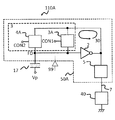
- the image pickup apparatus 100 includes a readout circuit 50A including a plurality of transistors.
- FIG. 1 shows the circuit configuration of the image pickup apparatus 100.
- the image pickup apparatus 100 includes a plurality of pixels 110A and peripheral circuits.
- the plurality of pixels 110A and peripheral circuits are provided on the semiconductor substrate 60.
- the plurality of pixels 110A and peripheral circuits are provided on a single semiconductor substrate 60.
- the plurality of pixels 110A and the peripheral circuit may be provided on separate semiconductor substrates.
- the plurality of pixels 110A are arranged two-dimensionally. As a result, a pixel array is formed.
- the plurality of pixels 110A are arranged in the row direction and the column direction.
- the row direction and the column direction refer to the directions in which the rows and columns extend respectively.
- the vertical direction that is, the vertical direction is the column direction.
- the horizontal direction that is, the left-right direction is the row direction.
- the center of each pixel 110A is located on the grid points of the square grid.
- the plurality of pixels 110A may be arranged in another form.
- the center of each pixel 110A may be located on a grid point such as a triangular grid or a hexagonal grid.
- the plurality of pixels 110A may be arranged one-dimensionally.
- the image pickup apparatus 100 may be a line sensor.
- the number of pixels 110A included in the image pickup apparatus 100 may be one.
- Each of the pixels 110A is connected to the power supply wiring 120.
- a predetermined power supply voltage is supplied to each pixel 110A via the power supply wiring 120.
- the imaging device 100 has a photoelectric conversion unit 17.
- the photoelectric conversion unit 17 photoelectrically converts the incident light. This creates an electric charge.
- each pixel 110A has a photoelectric conversion unit 17.
- the photoelectric conversion unit 17 is in the form of a film.
- the photoelectric conversion unit 17 is laminated on the semiconductor substrate 60.
- the image pickup device 100 constitutes a stacked image pickup device.
- the photoelectric conversion units 17 of the plurality of pixels 110A are continuously arranged on the semiconductor substrate 60 without any space between them. The same voltage is supplied to the entire photoelectric conversion unit 17 arranged continuously.
- the photoelectric conversion units 17 of the plurality of pixels 110A are arranged on the semiconductor substrate 60 at intervals from each other. Different voltages may be supplied to each photoelectric conversion unit 17.
- the peripheral circuit includes a control circuit 146, a voltage supply circuit 148, a vertical scanning circuit 141, a column signal processing circuit 142, a horizontal signal readout circuit 143, and a constant current source 144. Peripheral circuits may further include other signal processing circuits, output circuits, and the like.
- the voltage supply circuit 148 supplies a voltage to each pixel 110A via the storage control line 130. Specifically, the voltage supply circuit 148 supplies a voltage to the photoelectric conversion unit 17 via the storage control line 130.
- the voltage supply circuit 148 may be a circuit that converts a voltage supplied from a power source such as a battery into a predetermined voltage.
- the voltage supply circuit 148 may be a circuit that generates a predetermined voltage.
- the voltage supply circuit 148 may be a part of the vertical scanning circuit 141.
- the column signal processing circuit 142 is arranged for each row of the pixel array of pixels 110A.
- the constant current source 144 is arranged for each row of the pixel array of the pixels 110A.
- the vertical scanning circuit 141 is connected to the band control signal line CON1 and the selective control signal line CON3.
- the vertical scanning circuit 141 applies a predetermined voltage to the band control signal line CON1. This adjusts the signal charge feedback.
- the vertical scanning circuit 141 applies a predetermined voltage to the selection control signal line CON3. As a result, a row of the pixel array is selected, and a plurality of pixels 110A belonging to the row are selected. In this embodiment, the pixel 110A is selected in units of rows in this way. Then, the reading of the signal voltage of the selected pixel 110A and the reset of the pixel electrode are executed.
- the column signal processing circuit 142 may also be referred to as a row signal storage circuit.
- the vertical scanning circuit 141 may also be referred to as a row scanning circuit.
- the selection control signal line CON3 may also be referred to as an address signal line.
- the control circuit 146 controls the entire image pickup apparatus 100.
- the control circuit 146 receives command data, a clock, and the like. These are given from the outside of the image pickup apparatus 100, for example.
- control circuit 146 has a timing generator.
- the control circuit 146 supplies a drive signal to the vertical scanning circuit 141, the horizontal signal readout circuit 143, the voltage supply circuit 148, and the like.
- the arrow extending from the control circuit 146 schematically represents the flow of the output signal from the control circuit 146.
- the control circuit 146 can be realized, for example, by a microcontroller including one or more processors.
- the function of the control circuit 146 may be realized by a combination of a general-purpose processing circuit and software.
- the function of the control circuit 146 may be realized by hardware specialized for such processing.
- the pixels 110A arranged in each row are electrically connected to the column signal processing circuit 142 via the vertical signal line 170 corresponding to each row.
- the column signal processing circuit 142 performs noise suppression signal processing, analog-to-digital conversion (AD conversion), and the like.
- the noise suppression signal processing is, for example, correlated double sampling.
- the plurality of column signal processing circuits 142 are connected to the horizontal signal reading circuit 143.
- the horizontal signal reading circuit 143 reads signals from the plurality of column signal processing circuits 142 and outputs the signals to the horizontal common signal line 180.
- FIG. 2 shows the circuit configuration of pixel 110A.
- Pixel 110A includes a photoelectric conversion unit 17 and a readout circuit 50A.
- the photoelectric conversion unit 17 receives the incident light and generates a signal charge.
- the signal charge may be simply referred to as an electric charge.
- the photoelectric conversion unit 17 receives light incident and generates positive and negative charges.
- a positive charge is used as the signal charge.
- the positive and negative charges are hole-electron pairs.
- the read-out circuit 50A reads out the signal charge generated by the photoelectric conversion unit 17.
- the readout circuit 50A includes an amplifier 2, a band control unit 3, a charge storage unit FD, and an output selection unit 5.
- the charge storage unit FD stores the signal charge generated by the photoelectric conversion unit 17.
- the charge storage unit FD is a diffusion region provided on the semiconductor substrate 60.
- the input of the amplifier 2 is connected to the charge storage unit FD.
- the amplifier 2 amplifies the signal corresponding to the signal charge accumulated in the charge storage unit FD, and outputs the signal to the band control unit 3 and the output selection unit 5.
- the band control unit 3 includes a band control circuit 3A and a reset circuit 4A.
- the band control circuit 3A is supplied with at least three different voltages from the voltage control circuit 99.
- the band control circuit 3A exerts a band control function according to the supplied voltage.
- the band control circuit 3A limits the output signal of the amplifier 2 and outputs it to the charge storage unit FD.
- the reset circuit 4A resets the charge storage unit FD. Specifically, the reset circuit 4A resets the signal charge stored in the charge storage unit FD.
- a feedback circuit 30 which is a feedback loop via an amplifier 2, a band control unit 3, and a charge storage unit FD is formed.
- the signal read from the charge storage unit FD is amplified by the amplifier 2, band-limited by the band control circuit 3A, and returned to the charge storage unit FD.
- the output selection unit 5 is connected to the signal reading line 7.
- the signal readout line 7 corresponds to the vertical signal line 170 shown in FIG.
- the signal readout line 7 is shared by at least two pixels.
- the output selection unit 5 has a function of outputting the signal amplified by the amplifier 2 to the signal reading line 7.
- the output selection unit 5 has a function of supplying a current to the amplifier 2. These functions can be switched between each other.
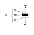
- FIG. 3A shows a photoelectric conversion unit 17A which is a specific example of the photoelectric conversion unit 17 of the present embodiment.
- FIG. 3B shows another specific example of the photoelectric conversion unit 17: the photoelectric conversion unit 17B.
- the photoelectric conversion unit 17A of FIG. 3A has a photoelectric conversion layer 17b, a counter electrode 17c, and a pixel electrode 17a.
- the photoelectric conversion layer 17b is sandwiched between the counter electrode 17c and the pixel electrode 17a.
- the photoelectric conversion unit 17A is laminated on the semiconductor substrate 60.
- the photoelectric conversion layer 17b is formed of an organic material or an inorganic material such as amorphous silicon.
- the photoelectric conversion layer 17b may include a layer made of an organic material and a layer made of an inorganic material.
- the photoelectric conversion layer 17b has a film shape. Typically, the photoelectric conversion layer 17b is continuously provided over the plurality of pixels 110A.
- the pixel electrode 17a is formed of a metal such as aluminum or copper, a metal nitride, or polysilicon or the like to which conductivity is imparted by doping with impurities.
- the pixel electrode 17a is spatially separated from the pixel electrodes 17a of other adjacent pixels 110A. As a result, the pixel electrode 17a is electrically separated from the pixel electrode 17a of the other pixel 110A.
- the counter electrode 17c is formed of a transparent conductive material such as ITO (Indium Tin Oxide). Therefore, the counter electrode 17c has translucency. “Translucency” refers to the property of transmitting at least a part of light having a wavelength that can be absorbed by the photoelectric conversion layer 17b, and it is not essential that light is transmitted over the entire wavelength range of visible light. Typically, the counter electrode 17c is continuously provided over the plurality of pixels 110A, similarly to the photoelectric conversion layer 17b.
- a reference voltage Vp is applied to the counter electrode 17c.
- the pixel electrode 17a is connected to the charge storage unit FD.
- the photoelectric conversion layer 17b converts light into electric charges.
- the pixel electrode 17a collects the charges generated by the photoelectric conversion layer 17b.
- the charge storage unit FD stores the charge collected by the pixel electrode 17a.
- the pixel 110A has a conductive structure that connects the pixel electrode 17a and the charge storage unit FD.
- the conductive structure may include a wiring layer, a plug, and the like. Illustration of the conductive structure is omitted in FIG. 3A.
- the photoelectric conversion unit 17B in FIG. 3B is a photodiode. Specifically, the photoelectric conversion unit 17B is provided on the semiconductor substrate 60.
- a reference voltage Vp is applied to one end of the photodiode which is the photoelectric conversion unit 17B. When reading a positive charge as a signal charge, the reference voltage Vp is typically a positive reference voltage.
- a charge storage unit FD is connected to the other end of the photodiode. Photodiodes generate an electric charge. The charge storage unit FD stores the charge generated by the photodiode.
- the photoelectric conversion unit 17 may be an element having another photoelectric conversion function.
- the pixel 110A and the readout circuit 50A will be further described with reference to FIG.
- the read-out circuit 50A includes an amplification transistor 200, a feedback transistor 301, a reset transistor 400, and a selection transistor 502.
- the amplification transistor 200, the feedback transistor 301, and the reset transistor 400 are N-type MOSFETs (Metal Oxide Semiconductor Field Effect Transistors).
- the selection transistor 502 is a P-type MOSFET.
- the N-type MOSFET may be referred to as an NMOS.
- a P-type MOSFET may be referred to as a MPa.
- which of the two diffusion regions of the MOSFET corresponds to the source and which corresponds to the drain is determined by the polarity of the MOSFET and the level of the potential at that time. Therefore, which corresponds to the source and which corresponds to the drain can vary depending on the operating state of the MOSFET.
- the imaging device so that which of the two diffusion regions of the MOSFET corresponds to the source and which corresponds to the drain is fixed.
- the source and drain fluctuate, and in some MOSFETs, the source and drain are fixed.
- the amplifier 2 has an amplification transistor 200 and a switching circuit 20.
- the amplification transistor 200 and the switching circuit 20 are connected to each other.
- the gate of the amplification transistor 200 is connected to the charge storage unit FD.
- One of the source and drain of the amplification transistor 200 is connected to one of the source and drain of the feedback transistor 301.
- One of the source and drain of the amplification transistor 200 is connected to one of the source and drain of the selection transistor 502.
- the switching circuit 20 includes a first switch element 11 and a second switch element 12.
- the switching circuit 20 is connected to the other of the source and drain of the amplification transistor 200.
- the other of the source and drain of the amplification transistor 200 can be connected to the first voltage source VA1 via the first switch element 11.
- the other of the source and drain of the amplification transistor 200 may also be connected to the second voltage source VA2 via the second switch element 12.
- the switching circuit 20 By controlling the switching circuit 20 with the control signals V1 and V2, the voltage applied to the other of the source and drain of the amplification transistor 200 can be switched to the voltage Va1 or the voltage Va2.
- the voltage Va1 of the first voltage source VA1 is, for example, the ground voltage GND.
- the voltage Va2 of the second voltage source VA2 is, for example, the power supply voltage VDD.
- the switching circuit 20 may be provided for each pixel. Alternatively, the switching circuit 20 may be shared by a plurality of pixels. Sharing the switching circuit 20 is advantageous from the viewpoint of reducing the number of elements per pixel.
- the band control circuit 3A includes a feedback transistor 301, a first capacitive element 9, and a second capacitive element 10.
- Capacitive element means a structure in which a dielectric such as an insulating film is sandwiched between electrodes.
- the “electrode” is not limited to an electrode formed of metal, and is interpreted to include a polysilicon layer or the like widely. The electrode may be a part of the semiconductor substrate 60.
- the first capacitive element 9 and the second capacitive element 10 may have a MIM (Metal Insulator Metal) capacitance.
- the first capacitive element 9 and the second capacitive element 10 may have a MIS (Metal Insulator Semiconductor) capacitance.
- One of the source and drain of the feedback transistor 301 is connected to one of the source and drain of the amplification transistor 200.
- One of the source and drain of the feedback transistor 301 is connected to one of the source and drain of the selection transistor 502.
- the other of the source and drain of the feedback transistor 301 is connected to one end of the first capacitive element 9.
- a reference voltage VR1 is applied to the other end of the first capacitance element 9.
- An RC filter circuit is formed by the feedback transistor 301 and the first capacitive element 9.
- the other of the source and drain of the feedback transistor 301 is also connected to one end of the second capacitive element 10.
- the other end of the second capacitance element 10 is connected to the charge storage unit FD.
- a node means an electrical connection between a plurality of elements in an electric circuit, and is a concept including wiring and the like that are responsible for the electrical connection between the elements.
- the band control signal line CON1 is connected to the gate of the feedback transistor 301.
- the reset circuit 4A includes a reset transistor 400.
- the reset transistor 400 includes a charge storage unit FD as one of a source and a drain.
- a node RD is connected to the other of the source and drain of the reset transistor 400.
- the gate of the reset transistor 400 is connected to the reset control signal line CON2.
- the state of the reset transistor 400 is determined by the voltage of the reset control signal line CON2. For example, when the voltage of the reset control signal line CON2 is at a high level, the reset transistor 400 is in the ON state. In this state, the charge storage unit FD is reset to the reference voltage VR2.
- the voltage of the node RD is applied to the reset transistor 400. In this way, the change in the voltage of the charge storage unit FD before and after turning off the reset transistor 400 can be reduced. This enables high-speed noise suppression.
- the output selection unit 5 includes a selection transistor 502.
- the selection transistor 502 has a polarity opposite to that of the amplification transistor 200.
- the amplification transistor 200 is an NMOS.
- the selection transistor 502 is a MOSFET.
- One of the source and drain of the selection transistor 502 is connected to one of the source and drain of the amplification transistor 200.
- the other of the source and drain of the selection transistor 502 is connected to the signal readout line 7.
- the gate of the selection transistor 502 is connected to the selection control signal line CON3.
- the state of the selection transistor 502 is determined by the voltage of the selection control signal line CON3.
- the selection transistor 502 when the voltage of the selection control signal line CON3 is low level, the selection transistor 502 is in the ON state. In this state, the amplification transistor 200 and the signal reading line 7 are electrically connected.
- the selection transistor 502 When the voltage of the selection control signal line CON3 is at a high level, the selection transistor 502 is in the off state. In this state, the amplification transistor 200 and the signal readout line 7 are electrically separated.
- the selective transistor 502 When the voltage of the selective control signal line CON3 is between the low level and the high level, the selective transistor 502 operates as a current source. As a result, a current is supplied to the amplification transistor 200. The amount of current is determined by the voltage of the selective control signal line CON3. The designer can design the readout circuit 50A so that the amount of current is desired.
- the voltage between the low level and the high level is, for example, an intermediate voltage between them.
- the switching circuit 40 is connected to the signal reading line 7.
- the switching circuit 40 includes a third switch element 13, a fourth switch element 14, voltage sources VB1 and VB2, and a constant current source 6.
- the constant current source 6 corresponds to the constant current source 144 shown in FIG.
- One terminal of the constant current source 6 can be connected to the signal reading line 7 via the third switch element 13.
- a voltage source VB2 may be connected to the signal readout line 7 via a fourth switch element 14.
- a voltage source VB1 is connected to the other terminal of the constant current source 6.
- the control signal V3 can be supplied to the third switch element 13.
- the control signal V4 may be supplied to the fourth switch element 14.
- the control signals V3 and V4 can be used to switch between connecting the voltage source VB2 and connecting the constant current source 6 to the signal reading line 7.
- the voltage Vb1 of the voltage source VB1 is, for example, the ground voltage GND.
- the voltage Vb2 of the voltage source VB2 is, for example, the power supply voltage VDD.
- the selection transistor 502 When the voltage source VB2 is connected to the signal reading line 7 and the voltage of the selection control signal line CON3 is a voltage between the low level and the high level, the selection transistor 502 operates as a current source. In that case, the selection transistor 502 and the amplification transistor 200 form an inverting amplifier circuit.
- the voltage between the low level and the high level is, for example, an intermediate voltage between them.
- the amplification transistor 200 and the constant current source 6 form a source follower circuit. In that case, the signal corresponding to the signal charge accumulated in the charge storage unit FD is output to the signal reading line 7 and read out to the outside.
- the constant current source 6 may be provided for each pixel.
- the constant current source 6 may be shared by a plurality of pixels. Sharing the constant current source 6 is advantageous from the viewpoint of reducing the number of elements per pixel.
- a feedback circuit 30 is formed.
- the feedback circuit 30 negatively feeds back the signal of the photoelectric conversion unit 17 to the charge storage unit FD via the amplification transistor 200.
- the state of the feedback transistor 301 is determined by the voltage of the band control signal line CON1.
- the feedback transistor 301 when the voltage of the band control signal line CON1 is at a high level, the feedback transistor 301 is in the ON state.
- the feedback circuit 30 is formed by the charge storage unit FD, the amplification transistor 200, the feedback transistor 301, and the second capacitive element 10.
- the resistance component of the feedback transistor 301 becomes large. Therefore, the band of the feedback transistor 301 is narrowed, and the frequency range of the feedback signal is narrowed.
- the signal output by the feedback transistor 301 is attenuated by the damping circuit including the parasitic capacitance of the second capacitance element 10 and the charge storage section FD, and is fed back to the charge storage section FD. ..
- the feedback transistor 301 When the voltage of the band control signal line CON1 becomes lower and becomes low level, the feedback transistor 301 is turned off. In the off state, the feedback circuit 30 is not formed.
- Patent Document 3 For details on the operation and control of the image pickup apparatus 100 according to the first embodiment, refer to Patent Document 3 and the like. The same applies to the second embodiment.
- FIG. 5 shows the circuit configuration of the pixel 110B and the readout circuit 50B according to the second embodiment.
- the switching circuit 40 has constant current sources 6A and 6B.
- the output selection unit 5 has a selection transistor 503 instead of the selection transistor 502.
- the polarity of the selection transistor 503 is the same as that of the amplification transistor 200 and the like.
- the selection transistor 503 is an NMOS.
- the constant current source 6A corresponds to the constant current source 6 shown in FIG. That is, the constant current source 6A corresponds to the constant current source 144 of FIG.
- the gate of the selection transistor 503 is connected to the selection control signal line CON3.
- the state of the selection transistor 503 is determined by the voltage of the selection control signal line CON3.
- the selection transistor 503 when the voltage of the selection control signal line CON3 is at a high level, the selection transistor 503 is in the ON state. In this state, the amplification transistor 200 and the signal reading line 7 are electrically connected.
- the selection transistor 503 When the voltage of the selection control signal line CON3 is low level, the selection transistor 503 is in the off state. In this state, the amplification transistor 200 and the signal readout line 7 are electrically separated.
- the pixel 110B has an inverting transistor 600 in addition to an amplification transistor 200, a feedback transistor 301, a reset transistor 400, and a selection transistor 503.
- the inverting transistor 600 has a polarity opposite to that of the amplification transistor 200, the feedback transistor 301, the reset transistor 400, and the selection transistor 503.
- the inverting transistor 600 is a MOSFET.
- the amplification transistor 200, the feedback transistor 301, the reset transistor 400, and the selection transistor 503 are NMOSs.
- the inverting transistor 600 can form a CMOS in cooperation with another transistor having a polarity opposite to that of the inverting transistor 600.
- CMOS complementary metal-oxide-semiconductor
- CMOS complementary metal-oxide-semiconductor
- an inverter that performs A / D conversion can be realized.
- CMOS can be formed by using the inverting transistor 600.
- the inverting transistor 600 may or may not be included in the readout circuit.
- the other transistor that constitutes CMOS in cooperation with the inverting transistor 600 may be a transistor shown in the figure or a transistor not shown in the figure.
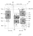
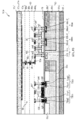
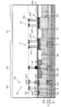
- FIG. 6 shows a schematic plan view of the pixel 110B according to the second embodiment.
- FIG. 7 is a schematic cross-sectional view of pixel 110B.
- FIG. 6 schematically shows the arrangement of each element provided on the semiconductor substrate 60 when the pixel 110B shown in FIG. 7 is viewed along the normal direction of the semiconductor substrate 60.
- the cross section shown in FIG. 7 is developed by cutting the pixel 110B along the VII-VII broken line in FIG. In FIG. 6, some elements are not shown.
- the pixel 110B includes a semiconductor substrate 60, a photoelectric conversion unit 17, a conductive structure 89, and an interlayer insulating layer 90.
- the conductive structure 89 is arranged above the semiconductor substrate 60. Specifically, the conductive structure 89 is arranged on the incident side of light when viewed from the semiconductor substrate 60.
- the semiconductor substrate 60 includes a support substrate 61, a P-type semiconductor region 61p, a P-well 65p, an N-well 65n, a diffusion region 67n, a diffusion region 68an, a diffusion region 68bn, a diffusion region 72ap, and a diffusion region 72bp. And the element separation region 69a and the element separation region 69b.
- the support substrate 61 is a P-type substrate. Specifically, the support substrate 61 is a P-type silicon substrate.
- the P-type semiconductor region 61p is arranged on the support substrate 61.
- the P-type semiconductor region 61p contains P-type impurities at a concentration lower than that of the support substrate 61.
- the P-well 65p is arranged in the P-type semiconductor region 61p.
- the P-well 65p contains P-type impurities at a concentration lower than that of the support substrate 61 and higher than that of the P-type semiconductor region 61p.
- the N well 65n is arranged in the P-type semiconductor region 61p.
- N-well 65n contains N-type impurities.
- the P well is a P-type impurity region.
- the N-well is an N-type impurity region.
- the “IMS Tr. Region” is a region in which the P well 65p expands in a plan view.
- the “MOSFET Tr. Region” is a region in which N wells 65n expand in a plan view.
- an insulating layer 70 is provided on the semiconductor substrate 60. Specifically, the insulating layer 70 covers a wide area on the semiconductor substrate 60.
- the reset transistor 400 includes a diffusion region 67n as one of a source and a drain.
- the reset transistor 400 includes a diffusion region 68 bn as the other of the source and drain.
- the reset transistor 400 includes an insulating layer 70 and a gate electrode 400e.
- the gate electrode 400e is provided on the insulating layer 70.
- the diffusion region 67n is also a charge storage unit FD.
- the diffusion region 67n temporarily stores the signal charge generated by the photoelectric conversion unit 17.
- the electric charge storage unit FD and the gate electrode 200e of the amplification transistor 200 are electrically connected to each other by a thick line.
- the feedback transistor 301 includes a diffusion region 68an as one of a source and a drain.
- the feedback transistor 301 includes a diffusion region 68 bn as the other of the source and drain.
- the feedback transistor 301 includes an insulating layer 70 and a gate electrode 301e.
- the gate electrode 301e is provided on the insulating layer 70.
- the inverting transistor 600 includes a diffusion region 72bp as one of a source and a drain.
- the inverting transistor 600 includes a diffusion region 72ap as the other of the source and drain.
- the inverting transistor 600 includes an insulating layer 70 and a gate electrode 600.
- the gate electrode 600 is provided on the insulating layer 70.
- Diffusion regions 67n, 68an and 68bn are N-type impurity regions.
- Diffusion regions 72ap and 72bp are P-type impurity regions.
- the diffusion region 67n is arranged in the P-type semiconductor region 61p.
- the diffusion region 67n includes a first region 67a and a second region 67b.
- the second region 67b is provided in the first region 67a.
- the second region 67b has a higher impurity concentration than the first region 67a.
- the diffusion regions 68an and 68bn are arranged in the P well 65p.
- Diffusion regions 72ap and 72bp are located within N wells 65n.
- the inverting transistor 600 is a MOSFET.
- the amplification transistor 200, the feedback transistor 301, the reset transistor 400, and the selection transistor 503 are NMOSs.
- the element separation region 69a electrically separates the inverting transistor 600, which is a MOSFET, from the amplification transistor 200, the feedback transistor 301, the reset transistor 400, and the selection transistor 503, which are NMOSs.
- the device separation region 69a is a region formed by injection separation.
- the device separation region 69a is an N-type impurity region.
- the device separation region 69a is an N-type impurity region having an impurity concentration higher than that of the N-well 65n.
- the element separation region 69b electrically separates the amplification transistor 200, the feedback transistor 301, the reset transistor 400, and the selection transistor 503, which are NMOSs, from the inverting transistor 600, which is a MOSFET.
- the device separation region 69b is a region formed by injection separation.
- the device separation region 69b is a P-type impurity region.
- the device separation region 69b is a P-type impurity region having an impurity concentration higher than that of the P-well 65p.
- the interlayer insulating layer 90 covers the semiconductor substrate 60.
- the interlayer insulating layer 90 supports the photoelectric conversion unit 17.
- a conductive structure 89 is arranged inside the interlayer insulating layer 90.
- the interlayer insulating layer 90 includes a plurality of insulating layers 90a, 90b, 90c and an insulating layer 90d.
- the number of insulating layers included in the interlayer insulating layer 90 is not particularly limited.
- the conductive structure 89 includes a plurality of wiring layers 80a, 80b and 80c.
- the conductive structure 89 includes a plurality of plugs pa1, pa2, pa3, pa4, pa5, pa6, pa7, pa8, pb, pc, pd, cg1, cg3 and cg5.
- a plug refers to a component used to connect elements.
- the material and structure of the plug are not particularly limited.
- the plug is a concept that includes a direct connection plug, a via plug, and a contact plug.
- the materials and structures of the direct connection plug, the via plug and the contact plug may be the same or different from each other.
- the direct connection plug is a plug that is directly connected to the wiring layer, and refers to a plug that is used to electrically connect the wiring layer to an element located on the semiconductor substrate side of the wiring layer.
- the direct connection plug is directly connected to the wiring layer closest to the semiconductor substrate.
- specific examples of "elements located closer to the semiconductor substrate than the wiring layer" regarding the electrical connection destination of the direct connection plug are a gate electrode, a contact plug, a diffusion region, or a conductive layer.
- An example of the material of the direct connection plug is a metal such as copper (Cu) or tungsten (W). In the illustrated example, the material of the direct plug is tungsten.
- the via plug refers to a plug that electrically connects the wiring layer and the wiring layer, or a plug that is used to electrically connect the wiring layer to an element located on the photoelectric conversion part side of the wiring layer.
- a specific example of the above-mentioned "via plug used for electrically connecting the wiring layer to an element located closer to the photoelectric conversion unit than the wiring layer” is that the wiring layer closest to the pixel electrode is electrically connected to the pixel electrode. Connect to.
- a via plug material is a metal such as copper (Cu) or tungsten (W).
- a specific example of the material for the via plug is copper.
- the contact plug is a plug containing impurities of the first conductive type or the second conductive type.
- the first conductive type and the second conductive type are different conductive types from each other.
- the first conductive type is N type or P type.
- the second conductive type is P type or N type.
- the contact plug is connected to, for example, a diffusion region or a gate electrode.
- the contact plug is interposed between the directly connected plug and the diffusion region or between the directly connected plug and the gate electrode in the pixel.
- the contact plug is interposed between the first element and the second element to realize a contact resistance between the first element and the contact plug, which is lower than the default resistance.
- it refers to a plug that is the contact resistance between the second element and the contact plug and realizes a contact resistance lower than the default resistance.
- the default resistance is the contact resistance between the first element and the second element when the first element and the second element are directly connected.
- the contact plug realizes low contact resistance by being interposed between the directly connected plug as the first element and the diffusion region as the second element.
- An example of a contact plug material is polysilicon.
- the plugs pb, pc and pd are via plugs.
- the plugs pa1, pa2, pa3, pa4, pa5, pa6, pa7, and pa8 are directly connected plugs.
- the plugs cg1, cg3 and cg5 are contact plugs.
- the plugs cg1, cg3 and cg5 have a film-shaped portion.
- the number of wiring layers included in the conductive structure 89 is not particularly limited.
- the number of plugs included in the conductive structure 89 is not particularly limited.
- the plurality of wiring layers may include a part or all of the band control signal line CON1, the reset control signal line CON2, and the selection control signal line CON3.
- the plugs cg1, cg3, cg5, pa1, pa2, pa3, pa4, pa5, pa6, pa7 and pa8 are arranged in the insulating layer 90a.
- the wiring layer 80a is arranged in the insulating layer 90a.
- the plug pb and the wiring layer 80b are arranged in the insulating layer 90b.
- the plug pc and the wiring layer 80c are arranged in the insulating layer 90c.
- the plug pd is arranged in the insulating layer 90d.
- the wiring layer 80a is electrically connected to the diffusion region 68an via the plug pa1 and the plug cg1 in this order.
- the wiring layer 80a is electrically connected to the diffusion region 68bn via the plug pa3 and the plug cg3 in this order.
- the wiring layer 80a is electrically connected to the diffusion region 72ap via the plug pa6.
- the wiring layer 80a is electrically connected to the diffusion region 72bp via the plug pa8.
- the diffusion region 68an includes a first region 68an1 and a second region 68an2.
- the second region 68an2 is provided in the first region 68an1.
- the second region 68an2 has a higher impurity concentration than the first region 68an1.
- the plug cg1 is connected to the second region 68an2.
- the diffusion region 68bn includes a first region 68bn1 and a second region 68bn2.
- the second region 68bn2 is provided in the first region 68bn1.
- the second region 68bn2 has a higher impurity concentration than the first region 68bn1.
- the plug cg3 is connected to the second region 68bn2.
- the wiring layer 80a is electrically connected to the gate electrode 301e via the plug pa2.
- the wiring layer 80a is electrically connected to the gate electrode 400e via the plug pa4.
- the wiring layer 80a is electrically connected to the gate electrode 600e via the plug pa7.
- the pixel electrode 17a is electrically connected to the diffusion region 67n, that is, the charge storage portion FD via the conductive structure 89. Specifically, the pixel electrode 17a passes through the plug pd, the wiring layer 80c, the plug pc, the wiring layer 80b, the plug pb, the wiring layer 80a, the plug pa5, and the plug cg5 in this order. It is electrically connected to the diffusion region 67n. Specifically, the plug cg5 is connected to the second region 67b of the diffusion region 67n.
- the wiring layers 80a, 80b and 80c are formed of a metal such as copper or tungsten, or a metal compound such as a metal nitride or a metal oxide.
- a metal such as copper or tungsten
- a metal compound such as a metal nitride or a metal oxide.
- the number of electric paths connecting the wiring layer 80a and the diffusion region 72ap is one, and specifically, the electric paths are configured by one plug.
- the number of parallel electric paths connecting the wiring layer 80a and the diffusion region 72ap may be plural, and specifically, such parallel electric paths may be configured by a plurality of plugs. In this way, the contact resistance between the electric paths and the diffusion region 72ap can be reduced as compared with the case where the number of electric paths is one. This can improve the performance of the characteristic transistor 600. The same applies to the number of electric paths connecting the wiring layer 80a and the diffusion region 72bp.
- the plugs (specifically, contact plugs) cg1, cg3 and cg5 are formed of polysilicon. Therefore, the conductivity of the plugs cg1, cg3 and cg5 can be increased, and the contact resistance between the plugs cg1, cg3 and cg5 and the diffusion regions 68an, 68bn and 67n can be reduced. This can improve the performance of the feedback transistor 301 and the reset transistor 400.
- the plugs cg1, cg3 and cg5 are N-type polysilicon plugs doped with N-type impurities.
- the N-type impurity is, for example, phosphorus.
- the plugs cg1, cg3 and cg5, and the gate electrodes 301e and 400e also have a film-shaped portion. Also, they are made of the same material. This means that these can be formed by a common film forming process, which is advantageous from the viewpoint of simplifying the manufacturing process.
- the plugs cg1, cg3 and cg5 and the gate electrodes 301e and 400e are formed of polysilicon.
- the photoelectric conversion unit 17 is a photoelectric conversion unit 17A including a pixel electrode 17a, a counter electrode 17c, and a photoelectric conversion layer 17b.
- the pixel electrode 17a is provided on the interlayer insulating layer 90. Specifically, the pixel electrode 17a is provided on the insulating layer 90d.
- the counter electrode 17c is arranged on the incident side of the light.
- the photoelectric conversion layer 17b is arranged between the pixel electrode 17a and the counter electrode 17c.
- the counter electrode 17c has a connection with the above-mentioned storage control line 130.
- the potential of the storage control line 130 is controlled to make the potential of the counter electrode 17c higher than the potential of the pixel electrode 17a.
- the positive charge among the positive and negative charges generated by the photoelectric conversion can be selectively collected by the pixel electrode 17a.
- the counter electrode 17c is a single layer continuous over the plurality of pixels 110B, it is possible to collectively apply a predetermined potential to the counter electrodes 17c of the plurality of pixels 110B.
- the pixel electrode 17a is electrically connected to the diffusion region 67n, that is, the charge storage portion FD via the conductive structure 89. Therefore, the electric charge collected by the pixel electrode 17a is transmitted to the diffusion region 67n via the conductive structure 89.
- the pixel electrode 17a passes through the plug pd, the wiring layer 80c, the plug pc, the wiring layer 80b, the plug pb, the wiring layer 80a, the plug pa5, and the plug cg5 in this order. It is electrically connected to the diffusion region 67n. Therefore, the electric charge collected by the pixel electrode 17a is transmitted to the diffusion region 67n via these in this order.
- the present embodiment will be further described using the terms such as the first transistor and the second transistor.
- the pixel 110B includes a photoelectric conversion unit 17, a charge storage unit FD, an amplification transistor 200 which is a first transistor, and an inverting transistor 600 which is a second transistor.
- the photoelectric conversion unit 17 converts light into electric charges.
- the charge storage unit FD stores the electric charge generated by the photoelectric conversion unit 17.
- the charge storage unit FD is a first conductive type diffusion region.
- the first transistor includes a source or drain containing first conductive type impurities.
- the second transistor includes a source or drain containing a second conductive type impurity.
- the second conductive type is different from the first conductive type.
- the conductive type differs between the charge storage unit FD and the source or drain of the second transistor.
- the source or drain of the second transistor may affect the charge storage unit FD.
- One example of the effect is the diffusion of conductive impurities different from the impurities contained in the charge storage unit FD from the second transistor to the charge storage unit FD.
- Another example of the effect is the influx of parasitic carriers generated in the second transistor from the second transistor into the charge storage section FD. As the pixel size shrinks, this effect is more likely to become apparent. This effect can cause leak currents and increase noise. Noise can degrade the image.
- the distance D2 between the charge storage unit FD and the inverting transistor 600, which is the second transistor, is the charge storage unit FD and the amplification transistor 200, which is the first transistor. Distance is longer than D1. Therefore, the above-mentioned influence can be suppressed. Therefore, this embodiment is suitable for reducing noise and obtaining a high-quality image.
- planar view means observing in a direction perpendicular to the surface of the semiconductor substrate 60.
- FIG. 6 represents the pixel 110B in a plan view.
- the distance D2 is the minimum distance between the charge storage unit FD and the source or drain of the inverting transistor 600, which is the second transistor, in a plan view.
- the distance D1 is the minimum distance between the charge storage unit FD and the gate electrode of the amplification transistor 200, which is the first transistor, in a plan view.
- FIG. 6 shows the distance D2 and the distance D1 in the first example.
- the outer edge of the diffusion region such as the source, drain, and charge storage portion FD is defined by a junction in which the concentration of the first conductive type impurity and the concentration of the second conductive type impurity are equal.
- the distance D2 is the distance between the centers of the charge storage unit FD and the source or drain of the inverting transistor 600, which is the second transistor, in a plan view.
- the distance D1 is the distance between the centers of the charge storage unit FD and the gate electrode of the amplification transistor 200, which is the first transistor, in a plan view.
- the center refers to the geometric center.
- the distance D2 is a connection portion between the charge storage portion FD and the conductive structure 89 and a connection portion between the source or drain of the inverting transistor 600 which is the second transistor and the conductive structure 89 in a plan view.
- the distance D1 is the distance between the connection portion between the charge storage portion FD and the conductive structure 89 and the connection portion between the gate electrode of the amplification transistor 200, which is the first transistor, and the conductive structure 89 in a plan view.
- the distance D2 is the distance between the centers of the charge storage unit FD and the gate electrode of the inverting transistor 600, which is the second transistor, in a plan view.
- the distance D1 is the distance between the centers of the charge storage unit FD and the gate electrode of the amplification transistor 200, which is the first transistor, in a plan view.
- the center refers to the geometric center.
- the distance D2 when the distance D2 is larger than the distance D1 in the plan view in any of the first example, the second example, the third example, and the fourth example, the distance D2 is larger than the distance D1 in the plan view. Will be treated as.
- the charge storage unit FD, the amplification transistor 200 which is the first transistor, and the inverting transistor 600 which is the second transistor are provided on a single semiconductor substrate 60.
- the above effects are likely to become apparent. Therefore, in the present embodiment, the effect of suppressing the above-mentioned influence is effectively exhibited by the magnitude relationship between the distances D2 and D1.
- the first transistor is an amplification transistor 200.
- the amplification transistor 200 generates a signal corresponding to the charge stored in the charge storage unit FD.
- the second transistor is an inverting transistor 600.
- the amplification transistor 200 which is the first transistor, is electrically connected to the charge storage unit FD.
- the gate of the first transistor is electrically connected to the charge storage unit FD.
- the inverting transistor 600 which is the second transistor, may also be electrically connected to the charge storage unit FD.
- the amplification transistor 200 which is the first transistor, is located in the first central region, which is the central region of the pixel 110B.
- the distance D2 can be easily made larger than the distance D1 in the plan view.
- the first central region of a pixel in plan view is a region similar to a pixel in plan view, the area is 70% of the area of the pixel, and the geometric center is the same as the geometric center of the pixel. It means a certain area.
- the amplification transistor 200 which is the first transistor, may be located in the second central region of the pixel 110B.
- the second central region of a pixel in plan view is a region similar to a pixel in plan view, the area is 40% of the area of the pixel, and the geometric center is the same as the geometric center of the pixel. means.
- the amplification transistor 200 which is the first transistor, may be located in the third central region of the pixel 110B.
- the third central region of a pixel in plan view is a region similar to a pixel in plan view, the area is 10% of the area of the pixel, and the geometric center is the same as the geometric center of the pixel. means.
- the outer edge of a pixel can be understood from, for example, a repeating array of pixels.
- a pixel is the smallest unit that can express gradation.
- the charge storage unit FD and the inverting transistor 600 which is the second transistor, are located on opposite sides of the amplification transistor 200, which is the first transistor, with respect to the CD1 in a certain direction.
- the charge storage unit FD, the first transistor, and the second transistor are arranged in this order with respect to the CD1 in a certain direction. In this way, the distance D2 can be easily made larger than the distance D1 in the plan view.
- the direction CD1 is the row direction.
- the direction CD1 may be in the column direction.
- the first conductive type is N type.
- the second conductive type is a P type.
- the amplification transistor 200 includes a source or drain containing N-type impurities. In this case, it is easier to secure the transconductance of the amplification transistor 200 as compared with the case where the amplification transistor 200 contains a source or drain containing P-type impurities. This is because electrons have higher mobility than holes. It is advantageous from the viewpoint of ensuring the performance of the amplification transistor 200 that it is easy to secure the transconductance.
- the pixel 110B has a first well region 65p and a second well region 65n.
- the first well region 65p contains a second conductive type impurity.
- the amplification transistor 200 which is the first transistor, is located in the first well region 65p.
- the second well region 65n contains first conductive type impurities.
- An inverting transistor 600 which is a second transistor, is located in the second well region 65n.
- the area of the first well region 65p is larger than the area of the second well region 65n.
- the area of the first well region 65p belonging to the pixel 110B is larger than the area of the second well region 65n belonging to the pixel 110B.
- the first well region 65p is a P well 65p.
- the second well region 65n is an N well region 65n.
- the image pickup apparatus 100 has a semiconductor substrate 60.
- this cross section may be referred to as, for example, a first cross section
- the source or drain of the amplification transistor 200 which is the first transistor
- the inverting transistor which is the second transistor. With 600 sources or drains, appears.
- the source or drain of the first transistor means at least one of the source and drain of the first transistor. The same applies to the source or drain of the second transistor.
- the source and drain of the first transistor and the source and drain of the second transistor appear.
- the charge storage portion FD also appears.
- the pixel 110B has an element separation region 69a and an element separation region 69b.
- the element separation region 69a separates the inverting transistor 600, which is the second transistor, from other elements.
- the element separation region 69b separates the reset transistor 400 whose polarity is inverted from that of the second transistor from other elements.
- the element separation region 69a and the element separation region 69b are formed by injection separation.
- the arrangement of the elements shown in the plan view of FIG. 6 can be applied to other embodiments.
- the element can be added to the plan view of FIG.
- the element can be eliminated from the plan view of FIG.
- the selection transistor 503 can be eliminated from the plan view of FIG. 6, and the selection transistor 502 can be used as the inverting transistor 600 to make other modifications.
- FIG. 8 shows a plan view applicable to the first embodiment.
- FIG. 9 is a schematic cross-sectional view of the pixel 110C.
- the conductive structure 89 includes a plurality of plugs cp1, cp2, cp3, cp4, cp5, cp6, cp7 and cp8. These plugs are arranged in the insulating layer 90a. These plugs have a rod-shaped portion. These plugs are specifically contact plugs.
- the wiring layer 80a is electrically connected to the diffusion region 68an via the plugs pa1 and cp1 in this order.
- the wiring layer 80a is electrically connected to the diffusion region 68bn via the plugs pa3 and cp3 in this order.
- the wiring layer 80a is electrically connected to the diffusion region 72ap via the plugs pa6 and cp6 in this order.
- the wiring layer 80a is electrically connected to the diffusion region 72bp via the plugs pa8 and cp8 in this order.
- the plug cp1 is connected to the second region 68an2 of the diffusion region 68an. Further, the plug cp3 is connected to the second region 68bn2 of the diffusion region 68bn.
- the diffusion region 72ap includes a first region 72ap1 and a second region 72ap2.
- the second region 72ap2 is provided in the first region 72ap1.
- the second region 72ap2 has a higher impurity concentration than the first region 72ap1.
- the plug cp6 is connected to the second region 72ap2.
- the diffusion region 72bp includes the first region 72bp1 and the second region 72bp2.
- the second region 72bp2 is provided in the first region 72bp1.
- the second region 72bp2 has a higher impurity concentration than the first region 72bp1.
- the plug cp8 is connected to the second region 72bp2.
- the wiring layer 80a is electrically connected to the gate electrode 301e via the plugs pa2 and cp2 in this order.
- the wiring layer 80a is electrically connected to the gate electrode 400e via the plugs pa4 and cp4 in this order.
- the wiring layer 80a is electrically connected to the gate electrode 600e via the plugs pa7 and cp7 in this order.
- the pixel electrode 17a is electrically connected to the diffusion region 67n, that is, the charge storage portion FD via the conductive structure 89. Specifically, the pixel electrode 17a passes through the plug pd, the wiring layer 80c, the plug pc, the wiring layer 80b, the plug pb, the wiring layer 80a, the plug pa5, and the plug cp5 in this order. It is electrically connected to the diffusion region 67n.
- the plugs (specifically, contact plugs) cp1, cp2, cp3, cp4, cp5, cp6, cp7 and cp8 are formed of polysilicon. Therefore, the conductivity of the plugs cp1, cp3, cp5, cp6 and cp8 can be increased, and the contact resistance between the plugs cp1, cp3, cp5, cp6 and cp8 and the diffusion regions 68an, 68bun, 67n, 72ap and 72bp can be reduced. ..
- the conductivity of the plugs cp2, cp4 and cp7 can be increased, and the contact resistance between the plugs cp2, cp4 and cp7 and the gate electrodes 301e, 400e and 600e can be reduced. This can improve the performance of the feedback transistor 301, the reset transistor 400 and the inverting transistor 600.
- the plurality of plugs cp1, cp2, cp3, cp4 and cp5 are N-type polysilicon plugs doped with N-type impurities.
- the N-type impurity is, for example, phosphorus.
- the plurality of plugs cp6, cp7 and cp8 are P-type polysilicon plugs doped with P-type impurities.
- the P-type impurity is, for example, boron.
- FIG. 10 shows a configuration example applicable to the pixel 110C.
- the configuration of FIG. 10 is also applicable to other embodiments.
- the region xp is a combination of the P-type semiconductor region 61p and the P-well 65p.
- the insulating layer 71 is provided so as to cover the gate electrodes 400e and 600e.
- the insulating layer 71 is, for example, a silicon oxide film.
- the insulating layer 71 may have a laminated structure.
- a sidewall 75 is provided on the insulating layer 71.
- the sidewall 75 is, for example, a silicon nitride film.
- the sidewall 75 is arranged between the plug cp3 and the gate electrode 400e.
- the sidewall 75 is arranged between the plug cp5 and the gate electrode 400e.
- the sidewall 75 is arranged between the plug cp5 and the plug cp6.
- the sidewall 75 is arranged between the plug cp6 and the gate electrode 600e.
- the sidewall 75 is arranged between the plug cp8 and the gate electrode 600e.
- the sidewall 75 overlaps with the diffusion region 68bn. In plan view, the sidewall 75 overlaps the diffusion region 67n. In plan view, the sidewall 75 overlaps with the diffusion region 72ap. In plan view, the sidewall 75 overlaps the diffusion region 72bp.
- Overlapping of two elements in plan view means that the two elements have at least partial overlap in plan view.
- the damage is, for example, the damage caused by the plasma used in the process after the formation of the diffusion region.
- Plasma damage is, for example, physical damage due to accelerated ion collisions and the creation of defects due to light.
- Light is, for example, ultraviolet light.
- the sidewall may be placed between the other plug and the gate electrode.
- the sidewalls may be arranged so as to overlap other diffusion regions in a plan view.
- the insulating layer 70 and the insulating layer 71 have a plurality of contact holes h3, h5, h6 and h8. These contact holes penetrate the insulating layer 70 and the insulating layer 71.
- the contact hole h3 overlaps with the diffusion region 68bn.
- a plug cp3 is arranged in the contact hole h3.
- the contact hole h5 overlaps with the diffusion region 67n.
- a plug cp5 is arranged in the contact hole h5.
- the contact hole h6 overlaps with the diffusion region 72ap.
- a plug cp6 is arranged in the contact hole h6.
- the contact hole h8 overlaps with the diffusion region 72bp.
- a plug cp8 is arranged in the contact hole h8.
- a contact hole may be formed at a position overlapping with another diffusion region in a plan view, and a plug may be placed in the contact hole.
- FIG. 11 is a schematic cross-sectional view of the pixel 110D.
- the conductive structure 89 includes a plurality of plugs cg6 and cg8.
- the plugs cg6 and cg8 are arranged in the insulating layer 90a.
- the plugs cg6 and cg8 have a film-shaped portion. Further, the plugs cg6 and cg8 are contact plugs.
- the wiring layer 80a is electrically connected to the diffusion region 72ap via the plug pa6 and the plug cg6 in this order.
- the wiring layer 80a is electrically connected to the diffusion region 72bp via the plug pa8 and the plug cg8 in this order.
- the plug cg6 is connected to the second region 72ap2 of the diffusion region 72ap. Further, the plug cg8 is connected to the second region 72bp2 of the diffusion region 72bp.
- the plugs cg6 and cg8 are formed of polysilicon. Therefore, the conductivity of the plugs cg6 and cg8 can be increased, and the contact resistance between the plugs cg6 and cg8 and the diffusion regions 72ap and 72bp can be reduced. This can improve the performance of the inverting transistor 600.
- the plurality of plugs cg6 and cg8 are P-type polysilicon plugs doped with P-type impurities.
- the P-type impurity is, for example, boron.
- both the plugs cg6 and cg8 and the gate electrode 600e have a film-shaped portion. Also, they are made of the same material. This means that these can be formed by a common film forming process, which is advantageous from the viewpoint of simplifying the manufacturing process. Specifically, the plugs cg6 and cg8 and the gate electrode 600e are formed of polysilicon.
- the third embodiment and the fourth embodiment will be further described using the terms such as the first transistor and the second transistor.
- Pixels 110C and 110D include a reset transistor 400 which is a first transistor, an inverting transistor 600 which is a second transistor, a first contact plug, and a second contact plug.
- the first transistor includes a diffusion region 67n or 68bn corresponding to a first diffusion region which is a source or drain, and a gate electrode 400e which is a first gate electrode containing a first conductive type impurity.
- the second transistor includes a diffusion region 72ap or 72bp corresponding to a second diffusion region which is a source or drain, and a second gate electrode 600e containing impurities of a second conductive type different from the first conductive type.
- the first contact plug is connected to the diffusion region 67n or 68bn, which is the first diffusion region, and contains the first conductive type impurities.
- the second contact plug is connected to the diffusion region 72ap or 72bp, which is the second diffusion region, and contains a second conductive type impurity.
- Both the gate electrode 400e, which is the first gate electrode, and the first contact plug are parts that contribute to the operation of the reset transistor 400, which is the first transistor.
- both of these portions contain first conductive type impurities. Doing so can contribute to ensuring the stability of operation of the first transistor. For example, when mass-producing an imaging device, quality variations are less likely to occur. This leads to obtaining a high-quality image. The same can be said for the configuration of the inverting transistor 600, which is the second transistor.
- the first contact plug is a plug cp3 or cp5.
- the second contact plug is a plug cp6 or cp8.
- the first contact plug is a plug cg3 or cg5.
- the second contact plug is a plug cg6 or cg8.
- the diffusion region 67n or 68bn which is the first diffusion region, contains the first conductive type impurities.
- the diffusion region 72ap or 72bp, which is the second diffusion region, contains a second conductive type impurity.
- the conductive type of the impurities in the first contact plug and the first diffusion region connected to each other is the same in the first conductive type.
- the conductive type of impurities in the second contact plug and the second diffusion region connected to each other is the same in the second conductive type. This is advantageous from the viewpoint of reducing the contact resistance between the first contact plug and the first diffusion region and improving the performance of the first transistor. It is also advantageous from the viewpoint of reducing the contact resistance between the second contact plug and the second diffusion region and improving the performance of the second transistor. These are advantageous from the viewpoint of obtaining a high-quality image.
- the first diffusion region includes a first region having a relatively low impurity concentration and a second region provided in the first region having a relatively high impurity concentration. Have. Then, the first contact plug is connected to the second region of the first diffusion region. In this case, the effect of reducing the contact resistance based on the first contact plug is likely to be effectively exhibited.
- the second diffusion region includes a first region having a relatively low impurity concentration and a second region provided in the first region having a relatively high impurity concentration.
- a second contact plug is connected to the second region of the second diffusion region. In this case, the effect of reducing the contact resistance based on the second contact plug is likely to be effectively exhibited.
- the first diffusion region is the charge storage unit FD.
- the charge storage unit FD stores charges.
- the first transistor is a reset transistor 400.
- the reset transistor 400 resets the charge storage unit FD.
- the second transistor is an inverting transistor 600.
- the first region of the first diffusion region is the first region 67a of the charge storage unit FD.
- the second region of the first diffusion region is the second region 67b of the charge storage unit FD.
- the first region of the second diffusion region is the first region 72ap1 or 72bp1.
- the second region of the second diffusion region is the second region 72ap2 or 72bp2.
- the first conductive type is N type.
- the second conductive type is P type.
- FIG. 12 is a schematic cross-sectional view of the pixel 110E.
- the element separation region 69c is used instead of the element separation region 69a.
- the element separation region 69c has an STI (Shallow Trench Isolation) structure.
- the element separation function can be easily secured even if the impurity concentration in the source and drain of the inverting transistor 600 is high. This is advantageous from the viewpoint of reducing the contact resistance between the plugs cg6 and cg8 and the diffusion regions 72ap and 72bp. This can improve the performance of the inverting transistor 600.
- the high element separation function based on the STI structure can also contribute to the reduction of pixel size.
- the plugs cg6 and cg8 are specifically contact plugs.
- the element separation region 69b is a region formed by injection separation.
- the device separation region 69c having the STI structure and the device separation region 69b formed by injection separation may be combined.
- the device separation region 69c having an STI structure is formed of, for example, a silicon oxide.
- the fifth embodiment will be further described using the terms such as the first transistor and the second transistor.
- Pixel 110E has an element separation region 69c.
- the element separation region 69c separates the second transistor 600 into elements.
- the element separation region 69c has an STI structure.
- the STI structure may have crystal defects on its side wall. Crystal defects can add noise to the charge storage section FD.
- the distance D3 between the charge storage unit FD and the element separation region 69c is longer than the distance D1 between the charge storage unit FD and the amplification transistor 200, which is the first transistor, in a plan view. This suppresses the generation of noise due to crystal defects in the charge storage portion FD, and is suitable for obtaining a high-quality image.
- the element separation region 69c is a region formed by injection separation, making the distance D3 longer than the distance D1 can contribute to the improvement of image quality. By doing so, it is possible to suppress the generation of noise due to high-concentration impurities in the injection separation region in the charge storage portion FD.
- the distance D3 is the minimum distance between the charge storage portion FD and the element separation region 69c in a plan view.
- the distance D1 is the minimum distance between the charge storage unit FD and the gate electrode of the amplification transistor 200, which is the first transistor, in a plan view.
- the element separation region 69c separates the inverting transistor 600, which is the second transistor, from the amplification transistor 200, which is the first transistor.
- a structure for suppressing a leak current between the element is provided between the element and the other element.
- the fact that an element is separated from another element means that, in plan view, the element is surrounded by the above structure and the other element is arranged outside the structure.
- Pixel 110E has an element separation region 69b.
- the element separation region 69b separates the reset transistor 400 whose polarity is inverted from that of the inverting transistor 600, which is the second transistor, from other elements.
- the element separation region 69c is formed by injection separation.
- the charge storage unit FD and the element separation region 69c are located on opposite sides of each other when viewed from the amplification transistor 200, which is the first transistor, in a certain direction. In this way, the distance D3 can be easily made longer than the distance D1 in a plan view.
- FIG. 13 is a schematic cross-sectional view of the pixel 110F.
- Pixel 110F has an N-type semiconductor region 62n.
- the N-type semiconductor region 62n divides the P-type semiconductor region 61p into a first region 61p1 in which the diffusion region 67n is arranged and a second region 61p2 different from the first region 61p1.
- the N-type semiconductor region 62n can suppress the inflow of minority carriers generated in the inverting transistor 600 or peripheral circuits into the charge storage unit FD. This is suitable for suppressing the leakage current due to the inflow of a small number of carriers into the charge storage portion FD and obtaining a high-quality image.
- the support substrate 61, the second region 61p2, the N-type semiconductor region 62n, and the first region 61p1 are arranged in this order. Further, the support substrate 61, the second region 61p2, the N-type semiconductor region 62n, and the P well 65p are arranged in this order.
- the second region 61p2 overlaps the P well 65p and the N well 65n. In a plan view, the second region 61p2 overlaps the charge storage unit FD. Further, in a plan view, the second region 61p2 overlaps at least one of the diffusion regions 72ap and 72bp, specifically both.
- Pixel 110F has at least one P-shaped region 64. Specifically, the pixel 110F has a plurality of P-shaped regions 64.
- the P-type region 64 has a higher impurity concentration than the support substrate 61 and the P-type semiconductor region 61p.
- the P-type region 64 electrically connects the support substrate 61, the P-type semiconductor region 61p, and the P-well 65p.
- the sixth embodiment will be further described using the terms such as the first semiconductor region and the second semiconductor region.
- the pixel 110F has a P-type semiconductor region 61p, which is a first semiconductor region, and an N-type semiconductor region 62n, which is a second semiconductor region.
- the second semiconductor region divides the first semiconductor region into a first region 61p1 and a second region 61p2 different from the first region 61p1.
- a charge storage unit FD is arranged in the first region 61p1. In a plan view, the second region 61p2 overlaps with the second well region N well 65n.
- the second region 61p2 overlapping the second well region in the plan view and the first region 61p1 in which the charge storage portion FD is arranged are the N-type semiconductor region which is the second semiconductor region. It is partitioned by 62n. Therefore, in this embodiment, it is possible to suppress the inflow of minority carriers generated in the inverting transistor 600, which is the second transistor, into the charge storage unit FD. This is suitable for suppressing the leakage current due to the inflow of a small number of carriers into the charge storage portion FD and obtaining a high-quality image.
- the first semiconductor region is the P-type semiconductor region 61p.
- the second semiconductor region is an N-type semiconductor region 62n.
- the second well region is the N well region 65n.
- the charge storage unit FD corresponds to the diffusion region 67n.
- FIG. 14 shows a schematic plan view of the pixel 110G according to the seventh embodiment.
- FIG. 15 shows a schematic cross-sectional view of the pixel 110G.
- FIG. 14 schematically shows the arrangement of each element provided on the semiconductor substrate 60 when the pixel 110G shown in FIG. 15 is viewed along the normal direction of the semiconductor substrate 60.
- the cross section shown in FIG. 15 is developed by cutting the pixel 110G along the XV-XV broken line in FIG.
- the conductive structure 89 includes plugs pa0, pa9, cg0 and cg9.
- the semiconductor substrate 60 includes a sub-contact region 66p and a well contact region 66n.
- the plugs pa0 and pa9 are directly connected plugs.
- the plugs cg0 and cg9 have a film-shaped portion. Further, the plugs cg0 and cg9 are contact plugs.
- the sub-contact region 66p has P-type impurities.
- the sub-contact region 66p is arranged within the P-well 65p.
- the sub-contact region 66p may be formed on the P-type element separation region.
- An element separation region 69b is arranged between the sub-contact region 66p and the diffusion region 68an.
- the well contact region 66n has N-type impurities.
- the well contact region 66n is arranged within the N well 65n.
- An element separation region 69c is arranged between the well contact region 66n and the diffusion region 72bp.
- the plugs pa0, pa9, cg0 and cg9 are arranged in the insulating layer 90a.
- the wiring layer 80a is electrically connected to the sub-contact region 66p via the plug pa0 and the plug cg0 in this order.
- the wiring layer 80a is electrically connected to the well contact region 66n via the plug pa9 and the plug cg9 in this order.
- the sub-contact region 66p includes the first region 66p1 and the second region 66p2.
- the second region 66p2 is provided in the first region 66p1.
- the second region 66p2 has a higher impurity concentration than the first region 66p1.
- the plug cg0 is connected to the second region 66p2.
- the well contact region 66n includes a first region 66n1 and a second region 66n2.
- the second region 66n2 is provided in the first region 66n1.
- the second region 66n2 has a higher impurity concentration than the first region 66n1.
- the plug cg9 is connected to the second region 66n2.
- the plugs (specifically, directly connected plugs) pa0 and pa9 are formed of a metal such as copper or tungsten, or a metal compound such as a metal nitride or a metal oxide.
- the plug (specifically, the contact plug) cg0 is formed of polysilicon.
- the plug cg0 is a P-type polysilicon plug doped with P-type impurities.
- the P-type impurity is, for example, boron.
- the plug (specifically, the contact plug) cg9 is formed of polysilicon.
- the plug cg9 is an N-type polysilicon plug doped with N-type impurities.
- the N-type impurity is, for example, phosphorus.
- a voltage can be supplied from the wiring layer 80a to the P well 65p via the plug pa0, the plug cg0, and the sub-contact region 66p in this order.
- a voltage can be supplied from the wiring layer 80a to the N well 65n via the plug pa9, the plug cg9, and the well contact region 66n in this order.
- one sub-contact area 66p and one well contact area 66n are provided for one pixel 110G.
- one sub-contact region 66p and one well contact region 66n may be provided for each of the plurality of pixels 110G.
- the plurality is, for example, four.
- the seventh embodiment will be further described using the terms such as the first well region and the second well region.
- the pixel 110G includes a P-well 65p which is a first well region, an N-well 65n which is a second well region, a sub-contact region 66p which is a first contact region, and a well contact region 66n which is a second contact region.
- the first well region contains a second conductive type impurity.
- the amplification transistor 200 which is the first transistor, is located in the first well region.
- the second well region contains first conductive type impurities.
- An inverting transistor 600 which is a second transistor, is located in the second well region.
- the first contact region contains a second conductive type impurity.
- the second contact region contains first conductive type impurities.
- a voltage is supplied to the first well region via the first contact region.
- a voltage is supplied to the second well region via the second contact region.
- each pixel 110G a voltage is supplied to the first well region via the first contact region.
- a voltage is supplied to the second well region via the second contact region.
- the first well region is a P well 65p.
- the second well region is the N well region 65n.
- the first contact region is a sub-contact region 66p.
- the second contact region is a well contact region 66n.
- the gate 200e of the amplification transistor 200 is located slightly above the center of the pixel 110G.
- the gate 200e of the amplification transistor 200 may be located at the center of the pixel 110G to the same extent as in FIG. 6 and the like in a plan view.
- a pixel array is composed of a plurality of pixels.
- an example of pixel arrangement in the pixel array will be described with reference to FIG.
- the pixel array AR1 in which a plurality of pixels 110B of the second embodiment are arranged will be described.
- a similar pixel array may be configured using the pixels described in other embodiments.
- one of the two pixels 110B adjacent to each other will be referred to as the first pixel 210A.
- the other of the two pixels 110B is referred to as a second pixel 210B.
- the charge storage unit FD of the first pixel 210A, the inverting transistor 600 which is the second transistor of the first pixel 210A, and the second transistor of the second pixel 210B are used for the CD1 in a certain direction.
- a certain inverting transistor 600 and the charge storage unit FD of the second pixel 210B are arranged in this order. In this way, the distance between the second transistor of the first pixel 210A and the charge storage unit FD of the second pixel 210B in the plan view is unlikely to be shortened. Further, in a plan view, the distance between the second transistor of the second pixel 210B and the charge storage unit FD of the first pixel 210A is unlikely to be shortened. This is suitable for obtaining a high-quality image.
- the second pixel 210B has a configuration that is line-symmetrically inverted with respect to the first pixel 210A.
- This inverted arrangement can be referred to as a flip arrangement.
- the second pixel 210B is horizontally inverted with respect to the first pixel 210A.
- the second pixel 210B may be upside down with respect to the first pixel 210A.
- the axis of line symmetry in plan view may extend in the column direction or in the row direction.
- the direction CD1 may be in the row direction or in the column direction.
- the first pixel 210A and the second pixel 210B share one P well 65p, which is a first well region. This is advantageous from the viewpoint of miniaturization of the image pickup apparatus.
- the fact that the first pixel 210A and the second pixel 201B share one first well region means that at least a part of the first well region belongs to the first pixel 210A and at least a part of the first well region is the second. It means that it belongs to pixel 210B.
- the first well region is P well 65p.
- the first pixel 210A and the second pixel 210B may share one second well region, N well 65n. This is advantageous from the viewpoint of miniaturization of the image pickup apparatus.
- the first pixel 210A and the second pixel 201B share one second well region, at least a part of the second well region belongs to the first pixel 210A and at least a part of the second well region is the second. It means that it belongs to pixel 210B.
- the second well region is N well 65n.
- the pixel array AR1 includes the third pixel 210C and the fourth pixel 210D.
- the third pixel 210C and the fourth pixel 210D correspond to the pixel 110B, respectively.
- the second pixel 210B and the third pixel 210C are adjacent to each other.
- the third pixel 210C and the fourth pixel 210D are adjacent to each other.
- the first pixel 210B, the second pixel 210B, the third pixel 210C, and the fourth pixel 210D are arranged in this order.
- the charge storage unit FD of the first pixel 210A, the inverting transistor 600 which is the second transistor of the first pixel 210A, and the second transistor of the second pixel 210B are used for the CD1 in a certain direction.
- the inverting transistor 600, which is a transistor, and the charge storage unit FD of the fourth pixel 210D are arranged in this order.
- the third pixel 210C has a configuration that is line-symmetrically inverted with respect to the second pixel 210B.
- the fourth pixel 210D has a configuration that is line-symmetrically inverted with respect to the third pixel 210C.
- a pixel array may be composed of a plurality of pixels.
- an example of supplying a voltage to the pixel array will be described with reference to FIGS. 17 to 19.
- a plurality of pixels 110H are arranged.
- the pixel array may be an array of a plurality of pixels described in other embodiments.
- FIG. 17 is a schematic plan view of the pixel region PR and the peripheral region SA.
- 18 and 19 are schematic cross-sectional views of the pixel region PR and its peripheral region SA.
- FIG. 17 schematically shows the arrangement of each element provided on the semiconductor substrate 60 when the pixels 110H shown in FIGS. 18 and 19 are viewed along the normal direction of the semiconductor substrate 60.
- the cross section shown in FIG. 18 is developed by cutting the structure along the XVIII-XVIII broken line in FIG.
- the cross section shown in FIG. 19 is developed by cutting the structure along the XIX-XIX broken line in FIG.
- the pixel area PR includes the pixel array AR2 and the margin area MR.
- the margin region MR surrounds the pixel array AR2.
- the peripheral area SA surrounds the pixel area PR.
- the contacts are electrically connected to the support substrate 61 in the peripheral region SA.
- the contact connects the support board 61 and the external circuit.
- the peripheral region SA includes a first portion P1 and a second portion P2.
- the interlayer insulating layer 90 and the conductive structure 89 are shared by the pixel region PR and the peripheral region SA.
- the wiring layer 80a is shared between the pixel region PR and the peripheral region SA.
- the wiring layer 80b, the wiring layer 80c, the wiring layer 80d, and the like may also be shared between the pixel region PR and the peripheral region SA.
- the support substrate 61, the P-type semiconductor region 61p, the N-type semiconductor region 62n, and the P-well 65p are shared by the pixel region PR and the peripheral region SA. Further, the pixel region PR and the peripheral region SA each have N wells 65n. In this example, the N well 65n of the pixel region PR and the N well 65n of the peripheral region SA are separated from each other.
- the semiconductor substrate 60 includes a diffusion region 73an and a diffusion region 73bn.
- the element separation region 69c is arranged between the pixel region PR and the peripheral region SA. In the peripheral region SA, the element separation region 69c is arranged between the first portion P1 and the second portion P2.
- the pixel region PR and the peripheral region SA each have a P-type region 64.
- the P-type region 64 electrically connects the support substrate 61 and the P well 65p.
- the P-type region 64 electrically connects the support substrate 61 and the P well 65p.
- the N-type semiconductor region 62n electrically connects the N-well 65n of the pixel region PR and the N-well 65n of the peripheral region SA. Specifically, the N-type semiconductor region 62n electrically connects the N-well 65n of the pixel 110H and the N-well 65n of the second portion P2.
- the conductive structure 89 has a plurality of plugs pa11, pa12, pa13 and pa14.
- the first portion P1 has conductive layers 81 and 82.
- the first portion P1 has a plurality of sub-contact regions yp1 and yp2.
- the plugs pa11, pa12, pa13 and pa14 are directly connected plugs.
- the plugs pa11 and pa12 are electrically connected to the conductive layer 81.
- the sub-contact region yp1 is interposed between the conductive layer 81 and the P-well 65p.
- the plugs pa13 and pa14 are electrically connected to the conductive layer 82.
- the sub-contact region yp2 is interposed between the conductive layer 82 and the P-well 65p.
- the conductive structure 89 has a plurality of plugs pa21, pa22, pa23 and pa24.
- the second portion P2 has conductive layers 83 and 84.
- the second portion P2 has a plurality of well contact regions Zn1 and Zn2.
- plugs pa21, pa22, pa23 and pa24 are directly connected plugs.
- the plugs pa21 and pa22 are electrically connected to the conductive layer 83.
- the well contact region Zn1 is interposed between the conductive layer 83 and the N well 65n of the second portion P2.
- the plugs pa23 and pa24 are electrically connected to the conductive layer 84.
- the well contact region Zn2 is interposed between the conductive layer 84 and the N well 65n of the second portion P2.
- the conductive structure 89 includes plugs pa41, pa42 and cg41.
- the plugs pa41 and pa42 are directly connected plugs.
- the plug cg41 has a film-shaped portion. Further, the plug cg41 is a contact plug.
- the plug cg41 penetrates the insulating layer 70.
- the plugs pa11, pa12, pa13, pa14, pa21, pa22, pa23, pa24, pa41, pa42, and cg41 are arranged in the insulating layer 90a.
- the amplification transistor 200 includes a diffusion region 73an as one of a source and a drain.
- the amplification transistor 200 includes a diffusion region 73bn as the other of the source and drain.
- the amplification transistor 200 includes an insulating layer 70 and a gate electrode 200e.
- the gate electrode 200 is provided on the insulating layer 70.
- the wiring layer 80a is electrically connected to the diffusion region 73an via the plug pa41 and the plug cg41 in this order.
- the wiring layer 80a is electrically connected to the gate electrode 200e via the plug pa42.
- the plug pa0, the plug cg0, and the sub-contact area 66p are arranged in the margin area MR.
- a plug pa9, a plug cg9, and a well contact region 66n are arranged in the margin region MR.
- the wiring layer 80a is electrically connected to the sub-contact region 66p via the plug pa0 and the plug cg0 in this order.
- the wiring layer 80a is electrically connected to the well contact region 66n via the plug pa9 and the plug cg9 in this order.
- the plugs (specifically, directly connected plugs) pa11, pa12, pa13, pa14, pa21, pa22, pa23, pa24, pa41 and pa42 are metals such as copper or tungsten, or metal compounds such as metal nitrides or metal oxides. Is formed from. The same applies to the conductive layers 81, 82, 83 and 84.
- the conductive layers 81 and 82 have the same potential because they are an integral conductive layer that is electrically connected. The same applies to the conductive layers 83 and 84.
- the plug (specifically, the contact plug) cg41 is formed of polysilicon.
- the plug cg41 is an N-type polysilicon plug doped with N-type impurities.
- the N-type impurity is, for example, phosphorus.
- the sub-contact regions yp1 and yp2 have P-type impurities.
- Well contact regions Zn1 and Zn2 have N-type impurities.
- a voltage can be supplied to the P well 65p via the wiring layer 80a, the plug pa0, the plug cg0, and the sub-contact region 66p in this order.
- a voltage can be supplied to the N well 65n through the wiring layer 80a, the plug pa9, the plug cg9, and the well contact region 66n in this order.
- the first row row1, the second row row2, the third row row3, the fourth row row4, and the like are set.
- a plurality of transistors are lined up.
- Each column of the plurality of columns including the first column row1, the second column row2, the third column row3, and the fourth column row4 has a sub-contact region 66p or a well contact region 66n in the margin region MR.
- Each row has one contiguous P-well 65p or one contiguous N-well 65n arranged to extend over both the margin region MR and the pixel array AR2. Therefore, in each row, the voltage can be stably supplied to the P well 65p or the N well 65n in the pixel array AR2. As a result, leakage current can be suppressed in a pixel array in which a plurality of different conductive transistors are arranged. This is suitable for obtaining a high-quality image.
- a plurality of columns share one continuous N-well 65n in the pixel array AR2.
- One sub-contact region 66p may be arranged in the margin region MR for each shared P-well 65p.
- one well contact region 66n may be arranged in the margin region MR.
- a voltage can be supplied to the P well 65p via the wiring layer 80a, the plugs pa11 and pa12, the conductive layer 81, and the sub-contact region yp1 in this order.
- a voltage can be supplied to the P well 65p via the wiring layer 80a, the plugs pa13 and pa14, the conductive layer 82, and the sub-contact region yp2 in this order. These voltage supplies can stabilize the voltage of the P well 65p.
- the wiring layer 80a, the plugs pa21 and pa22, the conductive layer 83, the well contact region zn1, the N well 65n of the second portion P2, and the N-type semiconductor region 62n are passed through in this order, and the pixel region PR
- a voltage can be supplied to the N well 65n of the above.
- a voltage can be supplied to the well 65n. These voltage supplies can stabilize the voltage of the N well 65n of the pixel region PR.
- the image pickup apparatus 100 includes a pixel region PR.
- the pixel region PR includes a pixel array AR2 and a margin region MR.
- the margin region MR surrounds the pixel array AR2.
- the pixel array AR2 includes a plurality of pixels 110H arranged in the direction CD2. These pixels 110H share one continuous first well region, the P well 65p.
- One continuous second well region, N well 65n, is shared by these pixels 110H.
- the margin region MR includes a sub-contact region 66p, which is a first contact region, and a well contact region 66n, which is a second contact region.
- a voltage is supplied to the one continuous first well region described above via the first contact region.
- a voltage is supplied to the one continuous second well region described above via the second contact region. In this way, the voltage can be efficiently supplied to the one continuous first well region described above. Further, in this way, the voltage can be efficiently supplied to the above-mentioned one continuous second well region.
- the first well region is a P well 65p.
- the second well region is the N well region 65n.
- the first contact region is a sub-contact region 66p.
- the second contact region is a well contact region 66n.
- the direction CD2 is the column direction, that is, the vertical direction, that is, the vertical direction in FIG.
- the direction CD2 may be in the row direction.
- the image pickup apparatus 100 includes a peripheral region SA.
- the peripheral region SA surrounds the pixel region PR.
- the semiconductor substrate 60 is shared by the peripheral region SA and the pixel region PR.
- a voltage is supplied from the peripheral region SA to at least one of the one continuous first well region and the one continuous second well region described above via an internal path in the semiconductor substrate 60.
- the gate 200e of the amplification transistor 200 is located slightly above the center of the pixel 110H.
- the gate 200e of the amplification transistor 200 may be located at the center of the pixel 110H to the same extent as in FIG. 6 and the like in a plan view.
- FIG. 20 shows the circuit configuration of the pixel 110I in the image pickup apparatus 100 according to the present embodiment.
- FIG. 21 is a plan view of pixel 110I.
- Pixel 110I includes a photodiode and a transfer transistor 700.
- the photodiode has an N-type impurity region 85n and a pinning layer.
- the pinning layer is located above the N-type impurity region 85n.
- the pinning layer is a P-type impurity region. In FIGS. 20 and 21, the illustration of the pinning layer is omitted.
- the photodiode generates an electric charge by photoelectrically converting the light received during the exposure time.
- the transfer signal is applied to the gate of the transfer transistor 700 via the transfer control signal line CON4.
- the transfer transistor 700 is turned on, and the charge generated by the photodiode is transferred to the charge storage unit FD.
- the amplification transistor 200 outputs a signal corresponding to the charge transferred to the charge storage unit FD to the signal reading line 7.
- the output signal can be used for signal processing such as AD conversion.
- the transfer transistor 700 includes a diffusion region 67n, which is a first diffusion region, as one of a source and a drain.
- the transfer transistor 700 includes an N-type impurity region 85n as the other of the source and drain. Included as source and drain. Further, the transfer transistor 700 includes a gate electrode 700e.
- the transfer transistor 700 shares a diffusion region 67n with the reset transistor 400 as one of a source and a drain. As described above, the diffusion region 67n corresponds to the charge storage unit FD.
- One of the source and drain of the reset transistor 400, the gate of the amplification transistor 200, and one of the source and drain of the transfer transistor 700 are electrically connected.
- an imaging device capable of taking high-quality images by suppressing the influence of leakage current.
- the image pickup apparatus of the present disclosure is useful for, for example, an image sensor, a digital camera, or the like.
- the imaging device of the present disclosure can be used for a medical camera, a robot camera, a security camera, a camera mounted on a vehicle, and the like.
Abstract
An imaging device according to an embodiment of the present disclosure comprises a pixel. The pixel includes a photoelectric conversion unit, a charge accumulating unit of a first conductivity type, a first transistor, and a second transistor. The photoelectric conversion unit converts light into electric charges. The charge accumulating unit accumulates the electric charges generated by the photoelectric conversion unit. The first transistor includes a first gate electrode and a first diffusion region which includes an impurity of the first conductivity type and which functions as a source or a drain. The second transistor includes a second gate electrode and a second diffusion region which includes an impurity of a second conductivity type and which functions as a source or a drain. The second conductivity type is different from the first conductivity type. In a plan view, a distance D2 between the charge accumulating unit and the second transistor is greater than a distance between the charge accumulating unit and the first transistor.
Description
本開示は、撮像装置に関する。
This disclosure relates to an imaging device.
デジタルカメラ等に、イメージセンサが用いられている。イメージセンサとしては、CCD(Charge Coupled Device)イメージセンサおよびCMOS(Complementary Metal Oxide Semiconductor)イメージセンサ等が例示される。
Image sensors are used in digital cameras, etc. Examples of the image sensor include a CCD (Charge Coupled Device) image sensor and a CMOS (Complementary Metal Oxide Semiconductor) image sensor.
一例に係るイメージセンサでは、半導体基板にフォトダイオードが設けられている。
In the image sensor according to an example, a photodiode is provided on the semiconductor substrate.
別例に係るイメージセンサでは、半導体基板の上方に光電変換層が設けられている。このような構造を有する撮像装置は、積層型の撮像装置と呼ばれることがある。
In the image sensor according to another example, a photoelectric conversion layer is provided above the semiconductor substrate. An image pickup device having such a structure is sometimes called a stacked image pickup device.
一具体例に係る積層型の撮像装置では、光電変換によって、信号電荷が生成される。生成された電荷は、半導体基板に設けられた拡散領域に一時的に蓄積される。蓄積された電荷量に応じた信号が、半導体基板に設けられたCCD回路またはCMOS回路を介して読み出される。
In the stacked image pickup device according to a specific example, a signal charge is generated by photoelectric conversion. The generated charge is temporarily accumulated in the diffusion region provided on the semiconductor substrate. A signal corresponding to the amount of accumulated charge is read out via a CCD circuit or a CMOS circuit provided on the semiconductor substrate.
特許文献1から3および非特許文献1では、撮像装置について記載されている。
Patent Documents 1 to 3 and Non-Patent Document 1 describe an imaging device.
高画質の画像を得るのに適した技術が要求されている。
Technology suitable for obtaining high-quality images is required.
本開示の一態様に係る撮像装置は、
少なくとも1つの画素を備える。
前記少なくとも1つの画素は、
光を電荷に変換する光電変換部と、
前記光電変換部で生成された前記電荷を蓄積する、第1導電型の電荷蓄積部と、
第1ゲート電極と、前記第1導電型の不純物を含み、ソースまたはドレインとして機能する第1拡散領域と、を含む第1トランジスタと、
第2ゲート電極と、前記第1導電型とは異なる第2導電型の不純物を含み、ソースまたはドレインとして機能する第2拡散領域と、を含む第2トランジスタと、を含む。
平面視において、前記電荷蓄積部と前記第2トランジスタとの距離は、前記電荷蓄積部と前記第1トランジスタとの距離より長い。 The imaging device according to one aspect of the present disclosure is
It has at least one pixel.
The at least one pixel
A photoelectric conversion unit that converts light into electric charges,
A first conductive type charge storage unit that stores the electric charge generated by the photoelectric conversion unit, and
A first transistor containing a first gate electrode and a first diffusion region containing the first conductive type impurities and functioning as a source or drain.
It includes a second gate electrode and a second transistor containing a second diffusion region containing impurities of a second conductive type different from the first conductive type and functioning as a source or drain.
In a plan view, the distance between the charge storage unit and the second transistor is longer than the distance between the charge storage unit and the first transistor.
本開示に係る技術は、高画質の画像を得るのに適している。
The technology according to the present disclosure is suitable for obtaining high-quality images.
(本開示に係る一態様の概要)
本開示の第1態様に係る撮像装置は、
少なくとも1つの画素を備える。
前記少なくとも1つの画素は、
光を電荷に変換する光電変換部と、
前記光電変換部で生成された前記電荷を蓄積する、第1導電型の電荷蓄積部と、
第1ゲート電極と、前記第1導電型の不純物を含み、ソースまたはドレインとして機能する第1拡散領域と、を含む第1トランジスタと、
第2ゲート電極と、前記第1導電型とは異なる第2導電型の不純物を含み、ソースまたはドレインとして機能する第2拡散領域と、を含む第2トランジスタと、を含む。
平面視において、前記電荷蓄積部と前記第2トランジスタとの距離は、前記電荷蓄積部と前記第1トランジスタとの距離より長い。 (Summary of one aspect relating to this disclosure)
The imaging device according to the first aspect of the present disclosure is
It has at least one pixel.
The at least one pixel
A photoelectric conversion unit that converts light into electric charges,
A first conductive type charge storage unit that stores the electric charge generated by the photoelectric conversion unit, and
A first transistor containing a first gate electrode and a first diffusion region containing the first conductive type impurities and functioning as a source or drain.
It includes a second gate electrode and a second transistor containing a second diffusion region containing impurities of a second conductive type different from the first conductive type and functioning as a source or drain.
In a plan view, the distance between the charge storage unit and the second transistor is longer than the distance between the charge storage unit and the first transistor.
第1態様に係る技術は、高画質の画像を得るのに適している。
The technique according to the first aspect is suitable for obtaining a high-quality image.
本開示の第2態様において、例えば、第1態様に係る撮像装置では、
前記少なくとも1つの画素は、前記第2トランジスタを素子分離する素子分離領域を含んでいてもよく、
平面視において、前記電荷蓄積部と前記素子分離領域との距離は、前記電荷蓄積部と前記第1トランジスタとの距離より長くてもよい。 In the second aspect of the present disclosure, for example, in the imaging device according to the first aspect,
The at least one pixel may include an element separation region for element separation of the second transistor.
In a plan view, the distance between the charge storage unit and the element separation region may be longer than the distance between the charge storage unit and the first transistor.
第2態様に係る技術は、高画質の画像を得るのに適している。
The technique according to the second aspect is suitable for obtaining a high-quality image.
本開示の第3態様において、例えば、第1または第2態様に係る撮像装置では、
前記第1トランジスタは、前記電荷蓄積部に蓄積された前記電荷に応じた信号を生成する増幅トランジスタであってもよい。 In the third aspect of the present disclosure, for example, in the imaging device according to the first or second aspect,
The first transistor may be an amplification transistor that generates a signal corresponding to the charge accumulated in the charge storage unit.
増幅トランジスタは、第1トランジスタの具体例である。
The amplification transistor is a specific example of the first transistor.
本開示の第4態様において、例えば、第1から第3態様のいずれか1つに係る撮像装置では、
平面視において、前記第1トランジスタは、前記少なくとも1つの画素の中央領域に位置していてもよい。 In the fourth aspect of the present disclosure, for example, in the imaging device according to any one of the first to third aspects,
In plan view, the first transistor may be located in the central region of the at least one pixel.
平面視において、前記第1トランジスタは、前記少なくとも1つの画素の中央領域に位置していてもよい。 In the fourth aspect of the present disclosure, for example, in the imaging device according to any one of the first to third aspects,
In plan view, the first transistor may be located in the central region of the at least one pixel.
第4態様によれば、第1態様の距離の大小関係を実現し易い。
According to the fourth aspect, it is easy to realize the magnitude relationship of the distance of the first aspect.
本開示の第5態様において、例えば、第1から第4態様のいずれか1つに係る撮像装置では、
平面視において、ある方向に沿って、前記電荷蓄積部、前記第1トランジスタおよび前記第2トランジスタが、この順に配置されていてもよい。 In the fifth aspect of the present disclosure, for example, in the imaging device according to any one of the first to fourth aspects,
In a plan view, the charge storage unit, the first transistor, and the second transistor may be arranged in this order along a certain direction.
第5態様によれば、第1態様の距離の大小関係を実現し易い。
According to the fifth aspect, it is easy to realize the magnitude relationship of the distance of the first aspect.
本開示の第6態様において、例えば、第1から第5態様のいずれか1つに係る撮像装置では、
前記第1導電型は、N型であってもよく、
前記第2導電型は、P型であってよい。 In the sixth aspect of the present disclosure, for example, in the image pickup apparatus according to any one of the first to fifth aspects,
The first conductive type may be N type.
The second conductive type may be a P type.
前記第1導電型は、N型であってもよく、
前記第2導電型は、P型であってよい。 In the sixth aspect of the present disclosure, for example, in the image pickup apparatus according to any one of the first to fifth aspects,
The first conductive type may be N type.
The second conductive type may be a P type.
N型は、第1導電型の具体例である。P型は、第2導電型の具体例である。
The N type is a specific example of the first conductive type. The P type is a specific example of the second conductive type.
本開示の第7態様において、例えば、第1から第6態様のいずれか1つに係る撮像装置では、
前記少なくとも1つの画素は、
前記第2導電型の不純物を含む第1ウェル領域と、
前記第1導電型の不純物を含む第2ウェル領域と、を含んでいてもよく、
平面視において、前記第1トランジスタは前記第1ウェル領域内に位置し、前記第2トランジスタは前記第2ウェル領域内に位置していてもよく、
平面視において、前記第1ウェル領域の面積は、前記第2ウェル領域の面積より大きくてもよい。 In the seventh aspect of the present disclosure, for example, in the imaging device according to any one of the first to sixth aspects,
The at least one pixel
The first well region containing the second conductive type impurities and
It may contain a second well region containing the first conductive type impurities.
In a plan view, the first transistor may be located in the first well region and the second transistor may be located in the second well region.
In a plan view, the area of the first well region may be larger than the area of the second well region.
第7態様の構成は、画素の構成の具体例である。
The configuration of the seventh aspect is a specific example of the pixel configuration.
本開示の第8態様において、例えば、第1から第7態様のいずれか1つに係る撮像装置では、
前記少なくとも1つの画素は、互いに隣接する第1画素および第2画素を含む複数の画素を備えていてもよく、
平面視において、ある方向に沿って、前記第1画素の前記電荷蓄積部と、前記第1画素の前記第2トランジスタと、前記第2画素の前記第2トランジスタと、前記第2画素の前記電荷蓄積部とは、この順に並んでいてもよい。 In the eighth aspect of the present disclosure, for example, in the imaging device according to any one of the first to seventh aspects,
The at least one pixel may include a plurality of pixels including a first pixel and a second pixel adjacent to each other.
In a plan view, the charge storage unit of the first pixel, the second transistor of the first pixel, the second transistor of the second pixel, and the charge of the second pixel along a certain direction. The storage units may be arranged in this order.
第8態様に係る技術は、高画質の画像を得るのに適している。
The technique according to the eighth aspect is suitable for obtaining a high-quality image.
本開示の第9態様において、例えば、第7態様に係る撮像装置では、
前記少なくとも1つの画素は、互いに隣接する第1画素および第2画素を含む複数の画素を備えていてもよく、
前記第1画素および前記第2画素は、1つの前記第1ウェル領域を共有していてもよい。 In the ninth aspect of the present disclosure, for example, in the imaging device according to the seventh aspect,
The at least one pixel may include a plurality of pixels including a first pixel and a second pixel adjacent to each other.
The first pixel and the second pixel may share one first well region.
第9態様は、撮像装置の小型化の観点から有利である。
The ninth aspect is advantageous from the viewpoint of miniaturization of the imaging device.
本開示の第10態様において、例えば、第1から第9態様のいずれか1つに係る撮像装置では、
前記光電変換部は、
光を電荷に変換する光電変換層と、
前記光電変換層で生成された前記電荷を収集する画素電極と、を含んでいてもよく、
前記電荷蓄積部は、前記画素電極で収集された前記電荷を蓄積してもよい。 In the tenth aspect of the present disclosure, for example, in the image pickup apparatus according to any one of the first to ninth aspects,
The photoelectric conversion unit
A photoelectric conversion layer that converts light into electric charges,
It may include a pixel electrode that collects the charge generated by the photoelectric conversion layer.
The charge storage unit may store the charge collected by the pixel electrode.
第10態様は、積層型の撮像装置を構成するのに適している。
The tenth aspect is suitable for forming a stacked image pickup device.
本開示の第11態様において、例えば、第10態様に係る撮像装置では、
前記少なくとも1つの画素は、前記画素電極と前記電荷蓄積部とを接続する導電構造を有していてもよい。 In the eleventh aspect of the present disclosure, for example, in the imaging device according to the tenth aspect,
The at least one pixel may have a conductive structure that connects the pixel electrode and the charge storage portion.
前記少なくとも1つの画素は、前記画素電極と前記電荷蓄積部とを接続する導電構造を有していてもよい。 In the eleventh aspect of the present disclosure, for example, in the imaging device according to the tenth aspect,
The at least one pixel may have a conductive structure that connects the pixel electrode and the charge storage portion.
第11態様は、光電変換部から電荷蓄積部に電荷を送るのに適している。
The eleventh aspect is suitable for sending charges from the photoelectric conversion unit to the charge storage unit.
本開示の第12態様において、例えば、第1から第9態様のいずれか1つに係る撮像装置では、
前記光電変換部は、フォトダイオードであってもよい。 In the twelfth aspect of the present disclosure, for example, in the imaging device according to any one of the first to ninth aspects,
The photoelectric conversion unit may be a photodiode.
前記光電変換部は、フォトダイオードであってもよい。 In the twelfth aspect of the present disclosure, for example, in the imaging device according to any one of the first to ninth aspects,
The photoelectric conversion unit may be a photodiode.
フォトダイオードは、光電変換部の具体例である。
The photodiode is a specific example of the photoelectric conversion unit.
本開示の第13態様において、例えば、第1から第12態様のいずれか1つに係る撮像装置では、
前記撮像装置は、半導体基板をさらに備えていてもよく、
前記半導体基板の主面に対して垂直な断面において、前記第1トランジスタの前記第1拡散領域と、前記第2トランジスタの前記第2拡散領域とが存在してもよい。 In the thirteenth aspect of the present disclosure, for example, in the image pickup apparatus according to any one of the first to twelfth aspects,
The image pickup apparatus may further include a semiconductor substrate.
The first diffusion region of the first transistor and the second diffusion region of the second transistor may be present in a cross section perpendicular to the main surface of the semiconductor substrate.
第13態様の構成は、画素の構成の具体例である。
本開示の第14態様において、例えば、第1から第13態様のいずれか1つに係る撮像装置では、
前記第1トランジスタの前記第1拡散領域は、前記電荷蓄積部と異なっていてもよい。
本開示の第15態様において、例えば、第1から第14態様のいずれか1つに係る撮像装置では、
平面視において、前記電荷蓄積部と前記第2トランジスタの前記第2ゲート電極との距離は、前記電荷蓄積部と前記第1トランジスタ前記第1ゲート電極との距離より長くてもよい。 The configuration of the thirteenth aspect is a specific example of the configuration of pixels.
In the fourteenth aspect of the present disclosure, for example, in the imaging device according to any one of the first to thirteenth aspects,
The first diffusion region of the first transistor may be different from the charge storage portion.
In the fifteenth aspect of the present disclosure, for example, in the imaging device according to any one of the first to the fourteenth aspects,
In a plan view, the distance between the charge storage unit and the second gate electrode of the second transistor may be longer than the distance between the charge storage unit and the first gate electrode of the first transistor.
本開示の第16態様に係る撮像装置は、
画素を備え、
前記画素は、
ソースまたはドレインである第1拡散領域と、第1導電型の不純物を含む第1ゲート電極と、を含む第1トランジスタと、
ソースまたはドレインである第2拡散領域と、前記第1導電型とは異なる第2導電型の不純物を含む第2ゲート電極と、を含む第2トランジスタと、
前記第1拡散領域に接続され、前記第1導電型の不純物を含む第1コンタクトプラグと、
前記第2拡散領域に接続され、前記第2導電型の不純物を含む第2コンタクトプラグと、を含む。 The imaging device according to the 16th aspect of the present disclosure is
Equipped with pixels,
The pixel is
A first transistor comprising a first diffusion region, which is a source or drain, and a first gate electrode containing first conductive impurities.
A second transistor including a second diffusion region, which is a source or drain, and a second gate electrode containing a second conductive type impurity different from the first conductive type.
A first contact plug connected to the first diffusion region and containing the first conductive type impurities,
Includes a second contact plug that is connected to the second diffusion region and contains the second conductive type impurities.
第16態様に係る技術は、高画質の画像を得るのに適している。
The technique according to the 16th aspect is suitable for obtaining a high-quality image.
本開示の第17態様において、例えば、第16態様に係る撮像装置では、
前記第1拡散領域は、前記第1導電型の不純物を含んでいてもよく、
前記第2拡散領域は、前記第2導電型の不純物を含んでいてもよい。 In the 17th aspect of the present disclosure, for example, in the imaging device according to the 16th aspect,
The first diffusion region may contain the first conductive type impurities.
The second diffusion region may contain the second conductive type impurities.
第1導電型は、第1拡散領域に含まれる不純物の導電型の具体例である。第2導電型は、第2拡散領域に含まれる不純物の導電型の具体例である。
The first conductive type is a specific example of the conductive type of impurities contained in the first diffusion region. The second conductive type is a specific example of the conductive type of impurities contained in the second diffusion region.
本開示の第18態様において、例えば、第16態様または第17態様に係る撮像装置では、
前記第1拡散領域は、電荷を蓄積する電荷蓄積部であってもよく、
前記第1トランジスタは、前記第1拡散領域の電位をリセットするリセットトランジスタであってもよい。 In the eighteenth aspect of the present disclosure, for example, in the image pickup apparatus according to the sixteenth aspect or the seventeenth aspect,
The first diffusion region may be a charge storage portion that stores charges.
The first transistor may be a reset transistor that resets the potential in the first diffusion region.
リセットトランジスタは、第1トランジスタの具体例である。
The reset transistor is a specific example of the first transistor.
本開示の第19態様に係る撮像装置は、
画素を備え、
前記画素は、
前記第1導電型の不純物を含むソースまたはドレインを含む第1トランジスタと、
前記第1導電型とは異なる第2導電型の不純物を含むソースまたはドレインを含む第2トランジスタと、を含む。 The imaging device according to the 19th aspect of the present disclosure is
Equipped with pixels,
The pixel is
A first transistor containing a source or drain containing the first conductive type impurities,
It includes a second transistor containing a source or drain containing impurities of the second conductive type different from the first conductive type.
第19態様の画素は、互いに反転した極性のトランジスタを有する。第19態様は、小型かつ高機能の撮像装置を実現するのに適している。第19態様の第1トランジスタの一例は増幅トランジスタであり、別例はリセットトランジスタである。
The pixels of the 19th aspect have transistors having polarities that are inverted from each other. The nineteenth aspect is suitable for realizing a compact and highly functional imaging device. An example of the first transistor of the nineteenth aspect is an amplification transistor, and another example is a reset transistor.
本開示の第20態様に係る撮像装置は、
画素を備え、
前記画素は、
ソースまたはドレインである第1拡散領域と、第1導電型の不純物を含む第1ゲート電極と、を含む第1トランジスタと、
前記第1拡散領域に接続され、前記第1導電型の不純物を含む第1プラグと、を含む。 The imaging device according to the 20th aspect of the present disclosure is
Equipped with pixels,
The pixel is
A first transistor comprising a first diffusion region, which is a source or drain, and a first gate electrode containing first conductive impurities.
It includes a first plug that is connected to the first diffusion region and contains the first conductive type impurities.
第20態様に係る技術は、高画質の画像を得るのに適している。第20態様の第1トランジスタの一例はリセットトランジスタである。
The technique according to the twentieth aspect is suitable for obtaining a high-quality image. An example of the first transistor of the twentieth aspect is a reset transistor.
本明細書では、第1、第2、第3・・・という序数詞を用いることがある。ある要素に序数詞が付されている場合に、より若番の同種類の要素が存在することは必須ではない。必要に応じて序数詞の番号を変更できる。
In this specification, the ordinal numbers such as first, second, third ... may be used. If an element has an ordinal number, it is not essential that a younger element of the same type exists. You can change the ordinal numbers as needed.
以下で説明する実施形態は、いずれも包括的または具体的な例を示す。以下の実施形態で示される数値、形状、材料、構成要素、構成要素の配置および接続形態、ステップ、ステップの順序等は、一例であり、本開示を限定する主旨ではない。本明細書において説明される種々の態様は、矛盾が生じない限り互いに組み合わせることが可能である。以下の説明において、実質的に同じ機能を有する構成要素は共通の参照符号で示し、説明を省略することがある。また、図面が過度に複雑になることを避けるために、一部の要素の図示を省略することがある。
The embodiments described below all show comprehensive or specific examples. Numerical values, shapes, materials, components, arrangement and connection forms of components, steps, step order, etc. shown in the following embodiments are examples, and are not intended to limit the present disclosure. The various aspects described herein can be combined with each other as long as there is no conflict. In the following description, components having substantially the same function are indicated by common reference numerals, and the description may be omitted. In addition, some elements may be omitted in order to avoid overly complicated drawings.
図面に示す各種の要素は、本開示の理解のために模式的に示したにすぎず、寸法比および外観等は実物と異なり得る。つまり、各図は、模式図であり、必ずしも厳密に図示されたものではない。したがって、例えば、各図において縮尺等は必ずしも一致しない。
The various elements shown in the drawings are only schematically shown for the purpose of understanding the present disclosure, and the dimensional ratio, appearance, etc. may differ from the actual ones. That is, each figure is a schematic view and is not necessarily exactly illustrated. Therefore, for example, the scales and the like do not always match in each figure.
包括的または具体的な態様は、素子、デバイス、モジュール、システムまたは方法で実現されてもよい。また、包括的または具体的な態様は、素子、デバイス、モジュール、システムおよび方法の任意の組み合わせによって実現されてもよい。
Comprehensive or specific embodiments may be implemented in elements, devices, modules, systems or methods. In addition, the comprehensive or specific embodiment may be realized by any combination of elements, devices, modules, systems and methods.
開示された実施形態の追加的な効果および利点は、明細書および図面から明らかになる。効果および/または利点は、明細書および図面に開示の様々な実施形態または特徴によって個々に提供され、これらの1つ以上を得るために全てを必要とはしない。
The additional effects and benefits of the disclosed embodiments will become apparent from the specification and drawings. The effects and / or advantages are provided individually by the various embodiments or features disclosed in the specification and drawings, and not all are required to obtain one or more of these.
以下の実施形態のトランジスタの極性および拡散領域の導電型は、一例である。矛盾のない限り、トランジスタの極性および拡散領域の導電型を反転させてもよい。
The polarity of the transistor and the conductive type in the diffusion region of the following embodiments are examples. As long as there is no contradiction, the polarity of the transistor and the conductive type in the diffusion region may be inverted.
(第1の実施形態)
以下、第1の実施形態に係る撮像装置100について説明する。撮像装置100は、複数のトランジスタを含む読み出し回路50Aを備える。 (First Embodiment)
Hereinafter, theimage pickup apparatus 100 according to the first embodiment will be described. The image pickup apparatus 100 includes a readout circuit 50A including a plurality of transistors.
以下、第1の実施形態に係る撮像装置100について説明する。撮像装置100は、複数のトランジスタを含む読み出し回路50Aを備える。 (First Embodiment)
Hereinafter, the
(撮像装置100の構造)
図1は、撮像装置100の回路構成を示す。撮像装置100は、複数の画素110Aと、周辺回路と、を備える。複数の画素110Aおよび周辺回路は、半導体基板60に設けられている。 (Structure of Imaging Device 100)
FIG. 1 shows the circuit configuration of theimage pickup apparatus 100. The image pickup apparatus 100 includes a plurality of pixels 110A and peripheral circuits. The plurality of pixels 110A and peripheral circuits are provided on the semiconductor substrate 60.
図1は、撮像装置100の回路構成を示す。撮像装置100は、複数の画素110Aと、周辺回路と、を備える。複数の画素110Aおよび周辺回路は、半導体基板60に設けられている。 (Structure of Imaging Device 100)
FIG. 1 shows the circuit configuration of the
本実施形態では、複数の画素110Aおよび周辺回路は、単一の半導体基板60に設けられている。ただし、複数の画素110Aと周辺回路とは、別々の半導体基板に設けられていてもよい。
In this embodiment, the plurality of pixels 110A and peripheral circuits are provided on a single semiconductor substrate 60. However, the plurality of pixels 110A and the peripheral circuit may be provided on separate semiconductor substrates.
撮像装置100では、複数の画素110Aは、2次元に配列されている。これにより、画素アレイが形成されている。
In the image pickup apparatus 100, the plurality of pixels 110A are arranged two-dimensionally. As a result, a pixel array is formed.
本実施形態では、複数の画素110Aは、行方向および列方向に配列されている。行方向および列方向とは、行および列がそれぞれ延びる方向をいう。図1において、垂直方向すなわち上下方向が、列方向である。水平方向すなわち左右方向が、行方向である。具体的には、各画素110Aの中心は、正方格子の格子点上に位置している。
In this embodiment, the plurality of pixels 110A are arranged in the row direction and the column direction. The row direction and the column direction refer to the directions in which the rows and columns extend respectively. In FIG. 1, the vertical direction, that is, the vertical direction is the column direction. The horizontal direction, that is, the left-right direction is the row direction. Specifically, the center of each pixel 110A is located on the grid points of the square grid.
複数の画素110Aは、他の形態で配列されていてもよい。例えば、各画素110Aの中心は、三角格子、六角格子等の格子点上に位置していてもよい。
The plurality of pixels 110A may be arranged in another form. For example, the center of each pixel 110A may be located on a grid point such as a triangular grid or a hexagonal grid.
複数の画素110Aは、1次元に配列されていてもよい。その場合、撮像装置100は、ラインセンサであってもよい。
The plurality of pixels 110A may be arranged one-dimensionally. In that case, the image pickup apparatus 100 may be a line sensor.
撮像装置100に含まれる画素110Aの数は、1つであってもよい。
The number of pixels 110A included in the image pickup apparatus 100 may be one.
画素110Aの各々は、電源配線120に接続されている。各画素110Aには、電源配線120を介して所定の電源電圧が供給される。
Each of the pixels 110A is connected to the power supply wiring 120. A predetermined power supply voltage is supplied to each pixel 110A via the power supply wiring 120.
撮像装置100は、光電変換部17を有する。光電変換部17は、入射光を光電変換する。これにより、電荷が生成される。典型例では、各画素110Aは、光電変換部17を有する。
The imaging device 100 has a photoelectric conversion unit 17. The photoelectric conversion unit 17 photoelectrically converts the incident light. This creates an electric charge. In a typical example, each pixel 110A has a photoelectric conversion unit 17.
本実施形態では、光電変換部17は、膜状である。光電変換部17は、半導体基板60に積層されている。こうして、撮像装置100は、積層型の撮像装置を構成している。
In this embodiment, the photoelectric conversion unit 17 is in the form of a film. The photoelectric conversion unit 17 is laminated on the semiconductor substrate 60. In this way, the image pickup device 100 constitutes a stacked image pickup device.
本実施形態では、複数の画素110Aの光電変換部17は、互いに間隔をあけずに半導体基板60上に連続的に配置されている。連続的に配置された光電変換部17の全体に、同一の電圧が供給される。
In the present embodiment, the photoelectric conversion units 17 of the plurality of pixels 110A are continuously arranged on the semiconductor substrate 60 without any space between them. The same voltage is supplied to the entire photoelectric conversion unit 17 arranged continuously.
別例では、複数の画素110Aの光電変換部17が、互いに間隔をあけて半導体基板60上に配置されている。それぞれの光電変換部17に対して、異なる電圧が供給され得る。
In another example, the photoelectric conversion units 17 of the plurality of pixels 110A are arranged on the semiconductor substrate 60 at intervals from each other. Different voltages may be supplied to each photoelectric conversion unit 17.
周辺回路は、制御回路146と、電圧供給回路148と、垂直走査回路141と、カラム信号処理回路142と、水平信号読み出し回路143と、定電流源144とを含む。周辺回路は、他の信号処理回路、出力回路等をさらに含んでいてもよい。
The peripheral circuit includes a control circuit 146, a voltage supply circuit 148, a vertical scanning circuit 141, a column signal processing circuit 142, a horizontal signal readout circuit 143, and a constant current source 144. Peripheral circuits may further include other signal processing circuits, output circuits, and the like.
電圧供給回路148は、蓄積制御線130を介して、各画素110Aに電圧を供給する。具体的には、電圧供給回路148は、蓄積制御線130を介して、光電変換部17に電圧を供給する。
The voltage supply circuit 148 supplies a voltage to each pixel 110A via the storage control line 130. Specifically, the voltage supply circuit 148 supplies a voltage to the photoelectric conversion unit 17 via the storage control line 130.
電圧供給回路148は、バッテリー等の電源から供給された電圧を所定の電圧に変換する回路であってもよい。電圧供給回路148は、所定の電圧を生成する回路であってもよい。電圧供給回路148は、垂直走査回路141の一部であってもよい。
The voltage supply circuit 148 may be a circuit that converts a voltage supplied from a power source such as a battery into a predetermined voltage. The voltage supply circuit 148 may be a circuit that generates a predetermined voltage. The voltage supply circuit 148 may be a part of the vertical scanning circuit 141.
本実施形態では、カラム信号処理回路142は、画素110Aの画素アレイの列毎に配置されている。定電流源144は、画素110Aの画素アレイの列毎に配置されている。
In this embodiment, the column signal processing circuit 142 is arranged for each row of the pixel array of pixels 110A. The constant current source 144 is arranged for each row of the pixel array of the pixels 110A.
垂直走査回路141は、帯域制御信号線CON1および選択制御信号線CON3に接続されている。
The vertical scanning circuit 141 is connected to the band control signal line CON1 and the selective control signal line CON3.
垂直走査回路141は、帯域制御信号線CON1に所定の電圧を印加する。これにより、信号電荷のフィードバックが調整される。
The vertical scanning circuit 141 applies a predetermined voltage to the band control signal line CON1. This adjusts the signal charge feedback.
垂直走査回路141は、選択制御信号線CON3に所定の電圧を印加する。これにより、画素アレイの行が選択され、その行に属する複数の画素110Aが選択される。本実施形態では、このように、行単位で画素110Aが選択される。そして、選択された画素110Aの信号電圧の読み出しと、画素電極のリセットとが実行される。
The vertical scanning circuit 141 applies a predetermined voltage to the selection control signal line CON3. As a result, a row of the pixel array is selected, and a plurality of pixels 110A belonging to the row are selected. In this embodiment, the pixel 110A is selected in units of rows in this way. Then, the reading of the signal voltage of the selected pixel 110A and the reset of the pixel electrode are executed.
カラム信号処理回路142は、行信号蓄積回路とも称され得る。垂直走査回路141は、行走査回路とも称され得る。選択制御信号線CON3は、アドレス信号線とも称され得る。
The column signal processing circuit 142 may also be referred to as a row signal storage circuit. The vertical scanning circuit 141 may also be referred to as a row scanning circuit. The selection control signal line CON3 may also be referred to as an address signal line.
制御回路146は、撮像装置100全体を制御する。この制御に際し、制御回路146は、指令データ、クロック等を受け取る。これらは、例えば、撮像装置100の外部から与えられる。
The control circuit 146 controls the entire image pickup apparatus 100. In this control, the control circuit 146 receives command data, a clock, and the like. These are given from the outside of the image pickup apparatus 100, for example.
典型的には、制御回路146は、タイミングジェネレータを有する。制御回路146は、垂直走査回路141、水平信号読み出し回路143、電圧供給回路148等に、駆動信号を供給する。図1において、制御回路146から延びる矢印は、制御回路146からの出力信号の流れを模式的に表している。
Typically, the control circuit 146 has a timing generator. The control circuit 146 supplies a drive signal to the vertical scanning circuit 141, the horizontal signal readout circuit 143, the voltage supply circuit 148, and the like. In FIG. 1, the arrow extending from the control circuit 146 schematically represents the flow of the output signal from the control circuit 146.
制御回路146は、例えば、1以上のプロセッサを含むマイクロコントローラによって実現され得る。制御回路146の機能は、汎用の処理回路とソフトウェアとの組み合わせによって実現されてもよい。制御回路146の機能は、このような処理に特化したハードウェアによって実現されてもよい。
The control circuit 146 can be realized, for example, by a microcontroller including one or more processors. The function of the control circuit 146 may be realized by a combination of a general-purpose processing circuit and software. The function of the control circuit 146 may be realized by hardware specialized for such processing.
各列に配置された画素110Aは、各列に対応した垂直信号線170を介して、カラム信号処理回路142に電気的に接続されている。カラム信号処理回路142は、雑音抑圧信号処理およびアナログ-デジタル変換(AD変換)等を行う。雑音抑圧信号処理は、例えば、相関二重サンプリングである。
The pixels 110A arranged in each row are electrically connected to the column signal processing circuit 142 via the vertical signal line 170 corresponding to each row. The column signal processing circuit 142 performs noise suppression signal processing, analog-to-digital conversion (AD conversion), and the like. The noise suppression signal processing is, for example, correlated double sampling.
複数のカラム信号処理回路142は、水平信号読み出し回路143に接続されている。水平信号読み出し回路143は、複数のカラム信号処理回路142から信号を読み出し、水平共通信号線180に信号を出力する。
The plurality of column signal processing circuits 142 are connected to the horizontal signal reading circuit 143. The horizontal signal reading circuit 143 reads signals from the plurality of column signal processing circuits 142 and outputs the signals to the horizontal common signal line 180.
次に、図2から図4を参照して、本実施形態に係る画素110Aの構造を説明する。
Next, the structure of the pixel 110A according to the present embodiment will be described with reference to FIGS. 2 to 4.
図2は、画素110Aの回路構成を示す。画素110Aは、光電変換部17および読み出し回路50Aを備える。
FIG. 2 shows the circuit configuration of pixel 110A. Pixel 110A includes a photoelectric conversion unit 17 and a readout circuit 50A.
光電変換部17は、光の入射を受けて、信号電荷を生成する。以下では、信号電荷を、単に電荷と称することがある。
The photoelectric conversion unit 17 receives the incident light and generates a signal charge. Hereinafter, the signal charge may be simply referred to as an electric charge.
具体的には、光電変換部17は、光の入射を受けて正および負の電荷を発生させる。本実施形態では、正の電荷が、信号電荷として用いられる。典型的には、正および負の電荷は、正孔-電子対である。
Specifically, the photoelectric conversion unit 17 receives light incident and generates positive and negative charges. In this embodiment, a positive charge is used as the signal charge. Typically, the positive and negative charges are hole-electron pairs.
読み出し回路50Aは、光電変換部17により生成された信号電荷を読み出す。読み出し回路50Aは、増幅器2、帯域制御部3、電荷蓄積部FDおよび出力選択部5を備える。
The read-out circuit 50A reads out the signal charge generated by the photoelectric conversion unit 17. The readout circuit 50A includes an amplifier 2, a band control unit 3, a charge storage unit FD, and an output selection unit 5.
電荷蓄積部FDは、光電変換部17によって生成された信号電荷を蓄積する。電荷蓄積部FDは、半導体基板60に設けられた拡散領域である。
The charge storage unit FD stores the signal charge generated by the photoelectric conversion unit 17. The charge storage unit FD is a diffusion region provided on the semiconductor substrate 60.
増幅器2の入力は、電荷蓄積部FDに接続されている。増幅器2は、電荷蓄積部FDに蓄積された信号電荷に応じた信号を増幅し、帯域制御部3および出力選択部5に出力する。
The input of the amplifier 2 is connected to the charge storage unit FD. The amplifier 2 amplifies the signal corresponding to the signal charge accumulated in the charge storage unit FD, and outputs the signal to the band control unit 3 and the output selection unit 5.
帯域制御部3は、帯域制御回路3Aおよびリセット回路4Aを含む。
The band control unit 3 includes a band control circuit 3A and a reset circuit 4A.
帯域制御回路3Aには、電圧制御回路99から、互いに異なる少なくとも3つの電圧が供給される。帯域制御回路3Aは、供給される電圧に応じた帯域制御機能を発揮する。帯域制御回路3Aは、増幅器2の出力信号に帯域制限をかけて、電荷蓄積部FDに出力する。
The band control circuit 3A is supplied with at least three different voltages from the voltage control circuit 99. The band control circuit 3A exerts a band control function according to the supplied voltage. The band control circuit 3A limits the output signal of the amplifier 2 and outputs it to the charge storage unit FD.
リセット回路4Aは、電荷蓄積部FDをリセットする。具体的には、リセット回路4Aは、電荷蓄積部FDに蓄積された信号電荷をリセットする。
The reset circuit 4A resets the charge storage unit FD. Specifically, the reset circuit 4A resets the signal charge stored in the charge storage unit FD.
撮像装置100では、増幅器2、帯域制御部3および電荷蓄積部FDを経由するフィードバックループであるフィードバック回路30が形成される。
In the image pickup apparatus 100, a feedback circuit 30 which is a feedback loop via an amplifier 2, a band control unit 3, and a charge storage unit FD is formed.
フィードバック回路30において、電荷蓄積部FDから読み出された信号は、増幅器2によって増幅され、帯域制御回路3Aによって帯域制限をかけられて、電荷蓄積部FDに帰還される。
In the feedback circuit 30, the signal read from the charge storage unit FD is amplified by the amplifier 2, band-limited by the band control circuit 3A, and returned to the charge storage unit FD.
出力選択部5は、信号読み出しライン7に接続されている。信号読み出しライン7は、図1に示される垂直信号線170に対応する。信号読み出しライン7は、少なくとも2つの画素で共有されている。
The output selection unit 5 is connected to the signal reading line 7. The signal readout line 7 corresponds to the vertical signal line 170 shown in FIG. The signal readout line 7 is shared by at least two pixels.
出力選択部5は、増幅器2によって増幅された信号を信号読み出しライン7に出力する機能を有する。出力選択部5は、増幅器2に電流を供給する機能を有する。これらの機能は互いに切り替えることができる。
The output selection unit 5 has a function of outputting the signal amplified by the amplifier 2 to the signal reading line 7. The output selection unit 5 has a function of supplying a current to the amplifier 2. These functions can be switched between each other.
図3Aに、本実施形態の光電変換部17の具体例である光電変換部17Aを示す。図3Bに、光電変換部17の別の具体例である光電変換部17Bを示す。
FIG. 3A shows a photoelectric conversion unit 17A which is a specific example of the photoelectric conversion unit 17 of the present embodiment. FIG. 3B shows another specific example of the photoelectric conversion unit 17: the photoelectric conversion unit 17B.
図3Aの光電変換部17Aは、光電変換層17bと、対向電極17cと、画素電極17aと、を有する。光電変換層17bは、対向電極17cおよび画素電極17aで挟まれている。光電変換部17Aは、半導体基板60上に積層されている。
The photoelectric conversion unit 17A of FIG. 3A has a photoelectric conversion layer 17b, a counter electrode 17c, and a pixel electrode 17a. The photoelectric conversion layer 17b is sandwiched between the counter electrode 17c and the pixel electrode 17a. The photoelectric conversion unit 17A is laminated on the semiconductor substrate 60.
光電変換層17bは、有機材料またはアモルファスシリコン等の無機材料から形成されている。光電変換層17bは、有機材料から構成される層と無機材料から構成される層とを含んでいてもよい。光電変換層17bは、膜形状を有する。典型的には、光電変換層17bは、複数の画素110Aにわたって連続的に設けられている。
The photoelectric conversion layer 17b is formed of an organic material or an inorganic material such as amorphous silicon. The photoelectric conversion layer 17b may include a layer made of an organic material and a layer made of an inorganic material. The photoelectric conversion layer 17b has a film shape. Typically, the photoelectric conversion layer 17b is continuously provided over the plurality of pixels 110A.
画素電極17aは、アルミニウム、銅等の金属、金属窒化物、または、不純物がドープされることにより導電性が付与されたポリシリコン等から形成されている。画素電極17aは、隣接する他の画素110Aの画素電極17aから空間的に分離されている。これにより、画素電極17aは、他の画素110Aの画素電極17aから電気的に分離されている。
The pixel electrode 17a is formed of a metal such as aluminum or copper, a metal nitride, or polysilicon or the like to which conductivity is imparted by doping with impurities. The pixel electrode 17a is spatially separated from the pixel electrodes 17a of other adjacent pixels 110A. As a result, the pixel electrode 17a is electrically separated from the pixel electrode 17a of the other pixel 110A.
対向電極17cは、ITO(Indium Tin Oxide)等の透明導電性材料から形成されている。このため、対向電極17cは、透光性を有する。「透光性」は、光電変換層17bが吸収可能な波長の光の少なくとも一部を透過する性質を指し、可視光の波長範囲全体にわたって光を透過することは必須ではない。典型的には、対向電極17cは、光電変換層17bと同様に、複数の画素110Aにわたって連続的に設けられている。
The counter electrode 17c is formed of a transparent conductive material such as ITO (Indium Tin Oxide). Therefore, the counter electrode 17c has translucency. “Translucency” refers to the property of transmitting at least a part of light having a wavelength that can be absorbed by the photoelectric conversion layer 17b, and it is not essential that light is transmitted over the entire wavelength range of visible light. Typically, the counter electrode 17c is continuously provided over the plurality of pixels 110A, similarly to the photoelectric conversion layer 17b.
対向電極17cに、基準電圧Vpが印加される。画素電極17aは、電荷蓄積部FDに接続されている。光電変換層17bは、光を電荷に変換する。画素電極17aは、光電変換層17bで生成された電荷を収集する。電荷蓄積部FDは、画素電極17aで収集された電荷を蓄積する。
A reference voltage Vp is applied to the counter electrode 17c. The pixel electrode 17a is connected to the charge storage unit FD. The photoelectric conversion layer 17b converts light into electric charges. The pixel electrode 17a collects the charges generated by the photoelectric conversion layer 17b. The charge storage unit FD stores the charge collected by the pixel electrode 17a.
具体的には、画素110Aは、画素電極17aと電荷蓄積部FDとを接続する導電構造を有する。導電構造は、配線層、プラグ等を含み得る。導電構造の図示は、図3Aでは省略されている。
Specifically, the pixel 110A has a conductive structure that connects the pixel electrode 17a and the charge storage unit FD. The conductive structure may include a wiring layer, a plug, and the like. Illustration of the conductive structure is omitted in FIG. 3A.
図3Bの光電変換部17Bは、フォトダイオードである。具体的には、光電変換部17Bは、半導体基板60に設けられている。
The photoelectric conversion unit 17B in FIG. 3B is a photodiode. Specifically, the photoelectric conversion unit 17B is provided on the semiconductor substrate 60.
光電変換部17Bであるフォトダイオードの一端に、基準電圧Vpが印加される。正の電荷を信号電荷として読み出す場合、典型的には、基準電圧Vpは、正の基準電圧である。フォトダイオードの他端に、電荷蓄積部FDが接続されている。フォトダイオードは、電荷を生成する。電荷蓄積部FDは、フォトダイオードで生成された電荷を蓄積する。
A reference voltage Vp is applied to one end of the photodiode which is the photoelectric conversion unit 17B. When reading a positive charge as a signal charge, the reference voltage Vp is typically a positive reference voltage. A charge storage unit FD is connected to the other end of the photodiode. Photodiodes generate an electric charge. The charge storage unit FD stores the charge generated by the photodiode.
光電変換部17は、その他の光電変換機能を有する素子であってもよい。
The photoelectric conversion unit 17 may be an element having another photoelectric conversion function.
図4を参照しながら、画素110Aおよび読み出し回路50Aについてさらに説明する。
The pixel 110A and the readout circuit 50A will be further described with reference to FIG.
読み出し回路50Aは、増幅トランジスタ200と、フィードバックトランジスタ301と、リセットトランジスタ400と、選択トランジスタ502と、を有する。増幅トランジスタ200、フィードバックトランジスタ301およびリセットトランジスタ400は、N型のMOSFET(Metal Oxide Semiconductor Field Effect Transistor)である。選択トランジスタ502は、P型のMOSFETである。
The read-out circuit 50A includes an amplification transistor 200, a feedback transistor 301, a reset transistor 400, and a selection transistor 502. The amplification transistor 200, the feedback transistor 301, and the reset transistor 400 are N-type MOSFETs (Metal Oxide Semiconductor Field Effect Transistors). The selection transistor 502 is a P-type MOSFET.
以下、N型のMOSFETをNMOSと称することがある。P型のMOSFETをPMOSと称することがある。
Hereinafter, the N-type MOSFET may be referred to as an NMOS. A P-type MOSFET may be referred to as a MPa.
本実施形態では、MOSFETの2つの拡散領域のうちどちらがソースに該当しどちらがドレインに該当するかは、MOSFETの極性およびその時点での電位の高低によって決定される。そのため、どちらがソースに該当しどちらがドレインに該当するかは、MOSFETの作動状態によって変動し得る。
In the present embodiment, which of the two diffusion regions of the MOSFET corresponds to the source and which corresponds to the drain is determined by the polarity of the MOSFET and the level of the potential at that time. Therefore, which corresponds to the source and which corresponds to the drain can vary depending on the operating state of the MOSFET.
ただし、MOSFETの2つの拡散領域のうちどちらがソースに該当しどちらがドレインに該当するかが固定されるように撮像装置を構成することも可能である。一部のMOSFETではソースおよびドレインが変動し、一部のMOSFETではソースおよびドレインが固定される形態も採用され得る。
However, it is also possible to configure the imaging device so that which of the two diffusion regions of the MOSFET corresponds to the source and which corresponds to the drain is fixed. In some MOSFETs, the source and drain fluctuate, and in some MOSFETs, the source and drain are fixed.
増幅器2は、増幅トランジスタ200と、切替回路20と、を有する。増幅トランジスタ200および切替回路20は、互いに接続されている。
The amplifier 2 has an amplification transistor 200 and a switching circuit 20. The amplification transistor 200 and the switching circuit 20 are connected to each other.
増幅トランジスタ200のゲートは、電荷蓄積部FDに接続されている。
The gate of the amplification transistor 200 is connected to the charge storage unit FD.
増幅トランジスタ200のソースおよびドレインの一方は、フィードバックトランジスタ301のソースおよびドレインの一方に接続されている。増幅トランジスタ200のソースおよびドレインの一方は、選択トランジスタ502のソースおよびドレインの一方と接続されている。
One of the source and drain of the amplification transistor 200 is connected to one of the source and drain of the feedback transistor 301. One of the source and drain of the amplification transistor 200 is connected to one of the source and drain of the selection transistor 502.
切替回路20は、第1のスイッチ素子11と、第2のスイッチ素子12と、を含む。切替回路20は、増幅トランジスタ200のソースおよびドレインの他方に接続されている。
The switching circuit 20 includes a first switch element 11 and a second switch element 12. The switching circuit 20 is connected to the other of the source and drain of the amplification transistor 200.
具体的には、増幅トランジスタ200のソースおよびドレインの他方は、第1のスイッチ素子11を介して、第1の電圧源VA1に接続され得る。増幅トランジスタ200のソースおよびドレインの他方は、第2のスイッチ素子12を介して、第2の電圧源VA2にも接続され得る。制御信号V1およびV2によって切替回路20を制御することにより、増幅トランジスタ200のソースおよびドレインの他方に印加する電圧を、電圧Va1または電圧Va2に切り替え可能である。
Specifically, the other of the source and drain of the amplification transistor 200 can be connected to the first voltage source VA1 via the first switch element 11. The other of the source and drain of the amplification transistor 200 may also be connected to the second voltage source VA2 via the second switch element 12. By controlling the switching circuit 20 with the control signals V1 and V2, the voltage applied to the other of the source and drain of the amplification transistor 200 can be switched to the voltage Va1 or the voltage Va2.
第1の電圧源VA1の電圧Va1は、例えば接地電圧GNDである。第2の電圧源VA2の電圧Va2は、例えば電源電圧VDDである。
The voltage Va1 of the first voltage source VA1 is, for example, the ground voltage GND. The voltage Va2 of the second voltage source VA2 is, for example, the power supply voltage VDD.
切替回路20は、画素毎に設けられていてもよい。あるいは、切替回路20は、複数の画素により共有されていてもよい。切替回路20の共有は、1画素あたりの素子数を削減する観点から有利である。
The switching circuit 20 may be provided for each pixel. Alternatively, the switching circuit 20 may be shared by a plurality of pixels. Sharing the switching circuit 20 is advantageous from the viewpoint of reducing the number of elements per pixel.
帯域制御回路3Aは、フィードバックトランジスタ301、第1の容量素子9および第2の容量素子10を含む。
The band control circuit 3A includes a feedback transistor 301, a first capacitive element 9, and a second capacitive element 10.
「容量素子」は、電極の間に絶縁膜等の誘電体が挟まれた構造を意味する。「電極」は、金属から形成された電極に限定されず、ポリシリコン層等を広く含むように解釈される。電極は、半導体基板60の一部分であってもよい。
"Capacitive element" means a structure in which a dielectric such as an insulating film is sandwiched between electrodes. The "electrode" is not limited to an electrode formed of metal, and is interpreted to include a polysilicon layer or the like widely. The electrode may be a part of the semiconductor substrate 60.
第1の容量素子9および第2の容量素子10は、MIM(Metal Insulator Metal)容量であってもよい。第1の容量素子9および第2の容量素子10は、MIS(Metal Insulator Semiconductor)容量であってもよい。
The first capacitive element 9 and the second capacitive element 10 may have a MIM (Metal Insulator Metal) capacitance. The first capacitive element 9 and the second capacitive element 10 may have a MIS (Metal Insulator Semiconductor) capacitance.
フィードバックトランジスタ301のソースおよびドレインの一方は、増幅トランジスタ200のソースおよびドレインの一方と接続されている。フィードバックトランジスタ301のソースおよびドレインの一方は、選択トランジスタ502のソースおよびドレインの一方と接続されている。
One of the source and drain of the feedback transistor 301 is connected to one of the source and drain of the amplification transistor 200. One of the source and drain of the feedback transistor 301 is connected to one of the source and drain of the selection transistor 502.
フィードバックトランジスタ301のソースおよびドレインの他方は、第1の容量素子9の一端に接続されている。第1の容量素子9の他端には、基準電圧VR1が印加される。フィードバックトランジスタ301と、第1の容量素子9とによって、RCフィルタ回路が形成される。
The other of the source and drain of the feedback transistor 301 is connected to one end of the first capacitive element 9. A reference voltage VR1 is applied to the other end of the first capacitance element 9. An RC filter circuit is formed by the feedback transistor 301 and the first capacitive element 9.
フィードバックトランジスタ301のソースおよびドレインの他方は、第2の容量素子10の一端にも接続されている。第2の容量素子10の他端は、電荷蓄積部FDに接続されている。
The other of the source and drain of the feedback transistor 301 is also connected to one end of the second capacitive element 10. The other end of the second capacitance element 10 is connected to the charge storage unit FD.
以下、フィードバックトランジスタ301、第1の容量素子9および第2の容量素子10の間に形成されたノードを「ノードRD」と称することがある。ここで、ノードは、電気回路における複数の要素間の電気的な接続部を意味し、該要素間の電気的な接続を担う配線等を含む概念である。
Hereinafter, the node formed between the feedback transistor 301, the first capacitive element 9 and the second capacitive element 10 may be referred to as a "node RD". Here, a node means an electrical connection between a plurality of elements in an electric circuit, and is a concept including wiring and the like that are responsible for the electrical connection between the elements.
フィードバックトランジスタ301のゲートには、帯域制御信号線CON1が接続されている。
The band control signal line CON1 is connected to the gate of the feedback transistor 301.
リセット回路4Aは、リセットトランジスタ400を含む。
The reset circuit 4A includes a reset transistor 400.
リセットトランジスタ400は、ソースおよびドレインの一方として、電荷蓄積部FDを含む。リセットトランジスタ400のソースおよびドレインの他方には、ノードRDが接続されている。リセットトランジスタ400のゲートは、リセット制御信号線CON2に接続されている。
The reset transistor 400 includes a charge storage unit FD as one of a source and a drain. A node RD is connected to the other of the source and drain of the reset transistor 400. The gate of the reset transistor 400 is connected to the reset control signal line CON2.
リセット制御信号線CON2の電圧により、リセットトランジスタ400の状態が決定される。例えば、リセット制御信号線CON2の電圧がハイレベルのとき、リセットトランジスタ400はオン状態である。この状態において、電荷蓄積部FDは、基準電圧VR2にリセットされる。
The state of the reset transistor 400 is determined by the voltage of the reset control signal line CON2. For example, when the voltage of the reset control signal line CON2 is at a high level, the reset transistor 400 is in the ON state. In this state, the charge storage unit FD is reset to the reference voltage VR2.
図4に示す読み出し回路50Aでは、ノードRDの電圧が、リセットトランジスタ400に印加される。このようにすると、リセットトランジスタ400をオフする前後における電荷蓄積部FDの電圧の変化を小さくできる。このことは、高速なノイズ抑制を可能にする。
In the read circuit 50A shown in FIG. 4, the voltage of the node RD is applied to the reset transistor 400. In this way, the change in the voltage of the charge storage unit FD before and after turning off the reset transistor 400 can be reduced. This enables high-speed noise suppression.
出力選択部5は、選択トランジスタ502を含む。
The output selection unit 5 includes a selection transistor 502.
本実施形態では、選択トランジスタ502は、増幅トランジスタ200の極性とは反転した極性を有する。具体的には、増幅トランジスタ200は、NMOSである。選択トランジスタ502は、PMOSである。
In the present embodiment, the selection transistor 502 has a polarity opposite to that of the amplification transistor 200. Specifically, the amplification transistor 200 is an NMOS. The selection transistor 502 is a MOSFET.
選択トランジスタ502のソースおよびドレインの一方は、増幅トランジスタ200のソースおよびドレインの一方と接続されている。選択トランジスタ502のソースおよびドレインの他方は、信号読み出しライン7に接続されている。
One of the source and drain of the selection transistor 502 is connected to one of the source and drain of the amplification transistor 200. The other of the source and drain of the selection transistor 502 is connected to the signal readout line 7.
選択トランジスタ502のゲートは、選択制御信号線CON3に接続されている。選択制御信号線CON3の電圧により、選択トランジスタ502の状態が決定される。
The gate of the selection transistor 502 is connected to the selection control signal line CON3. The state of the selection transistor 502 is determined by the voltage of the selection control signal line CON3.
例えば、選択制御信号線CON3の電圧がローレベルのとき、選択トランジスタ502はオン状態である。この状態において、増幅トランジスタ200と信号読み出しライン7とは、電気的に接続される。
For example, when the voltage of the selection control signal line CON3 is low level, the selection transistor 502 is in the ON state. In this state, the amplification transistor 200 and the signal reading line 7 are electrically connected.
選択制御信号線CON3の電圧がハイレベルのとき、選択トランジスタ502は、オフ状態である。この状態において、増幅トランジスタ200と信号読み出しライン7とは、電気的に分離される。
When the voltage of the selection control signal line CON3 is at a high level, the selection transistor 502 is in the off state. In this state, the amplification transistor 200 and the signal readout line 7 are electrically separated.
選択制御信号線CON3の電圧がローレベルとハイレベルとの間の電圧であるとき、選択トランジスタ502は電流源として動作する。これにより、増幅トランジスタ200に電流が供給される。その電流量は選択制御信号線CON3の電圧によって決定される。設計者は、所望の電流量になるように、読み出し回路50Aを設計できる。ローレベルとハイレベルとの間の電圧は、例えば、これらの中間の電圧である。
When the voltage of the selective control signal line CON3 is between the low level and the high level, the selective transistor 502 operates as a current source. As a result, a current is supplied to the amplification transistor 200. The amount of current is determined by the voltage of the selective control signal line CON3. The designer can design the readout circuit 50A so that the amount of current is desired. The voltage between the low level and the high level is, for example, an intermediate voltage between them.
切替回路40は、信号読み出しライン7に接続されている。切替回路40は、第3のスイッチ素子13と、第4のスイッチ素子14と、電圧源VB1およびVB2と、定電流源6とを含む。定電流源6は、図1に示される定電流源144に対応する。
The switching circuit 40 is connected to the signal reading line 7. The switching circuit 40 includes a third switch element 13, a fourth switch element 14, voltage sources VB1 and VB2, and a constant current source 6. The constant current source 6 corresponds to the constant current source 144 shown in FIG.
信号読み出しライン7には、第3のスイッチ素子13を介して定電流源6の一方の端子が接続され得る。信号読み出しライン7には、第4のスイッチ素子14を介して電圧源VB2が接続され得る。定電流源6の他方の端子には、電圧源VB1が接続されている。
One terminal of the constant current source 6 can be connected to the signal reading line 7 via the third switch element 13. A voltage source VB2 may be connected to the signal readout line 7 via a fourth switch element 14. A voltage source VB1 is connected to the other terminal of the constant current source 6.
第3のスイッチ素子13に、制御信号V3が供給され得る。第4のスイッチ素子14に、制御信号V4が供給され得る。制御信号V3およびV4により、信号読み出しライン7に、電圧源VB2を接続するか、定電流源6を接続するかを切替えることができる。
The control signal V3 can be supplied to the third switch element 13. The control signal V4 may be supplied to the fourth switch element 14. The control signals V3 and V4 can be used to switch between connecting the voltage source VB2 and connecting the constant current source 6 to the signal reading line 7.
電圧源VB1の電圧Vb1は、例えば、接地電圧GNDである。電圧源VB2の電圧Vb2は、例えば、電源電圧VDDである。
The voltage Vb1 of the voltage source VB1 is, for example, the ground voltage GND. The voltage Vb2 of the voltage source VB2 is, for example, the power supply voltage VDD.
電圧源VB2が信号読み出しライン7に接続されており、かつ、選択制御信号線CON3の電圧がローレベルとハイレベルとの間の電圧であるとき、選択トランジスタ502は電流源として動作する。その場合、選択トランジスタ502と、増幅トランジスタ200とは反転増幅回路を形成する。ローレベルとハイレベルとの間の電圧は、例えば、これらの中間の電圧である。
When the voltage source VB2 is connected to the signal reading line 7 and the voltage of the selection control signal line CON3 is a voltage between the low level and the high level, the selection transistor 502 operates as a current source. In that case, the selection transistor 502 and the amplification transistor 200 form an inverting amplifier circuit. The voltage between the low level and the high level is, for example, an intermediate voltage between them.
定電流源6が信号読み出しライン7に接続されており、かつ、選択制御信号線CON3の電圧がローレベルであるとき、増幅トランジスタ200と、定電流源6とは、ソースフォロア回路を形成する。その場合、電荷蓄積部FDに蓄積された信号電荷に応じた信号が、信号読み出しライン7に出力され、外部に読み出される。
When the constant current source 6 is connected to the signal reading line 7 and the voltage of the selective control signal line CON3 is low level, the amplification transistor 200 and the constant current source 6 form a source follower circuit. In that case, the signal corresponding to the signal charge accumulated in the charge storage unit FD is output to the signal reading line 7 and read out to the outside.
定電流源6は、画素毎に設けられていてもよい。定電流源6は、複数の画素により共有されていてもよい。定電流源6の共有は、1画素あたりの素子数を削減する観点から有利である。
The constant current source 6 may be provided for each pixel. The constant current source 6 may be shared by a plurality of pixels. Sharing the constant current source 6 is advantageous from the viewpoint of reducing the number of elements per pixel.
撮像装置100では、フィードバック回路30が形成される。フィードバック回路30により、光電変換部17の信号が、増幅トランジスタ200を介して電荷蓄積部FDに負帰還される。
In the image pickup apparatus 100, a feedback circuit 30 is formed. The feedback circuit 30 negatively feeds back the signal of the photoelectric conversion unit 17 to the charge storage unit FD via the amplification transistor 200.
帯域制御信号線CON1の電圧によりフィードバックトランジスタ301の状態が決定される。
The state of the feedback transistor 301 is determined by the voltage of the band control signal line CON1.
例えば、帯域制御信号線CON1の電圧がハイレベルのとき、フィードバックトランジスタ301はオン状態である。その場合、電荷蓄積部FDと、増幅トランジスタ200と、フィードバックトランジスタ301と、第2の容量素子10とによってフィードバック回路30が形成される。
For example, when the voltage of the band control signal line CON1 is at a high level, the feedback transistor 301 is in the ON state. In that case, the feedback circuit 30 is formed by the charge storage unit FD, the amplification transistor 200, the feedback transistor 301, and the second capacitive element 10.
帯域制御信号線CON1の電圧が低くなると、フィードバックトランジスタ301の抵抗成分が大きくなる。そのため、フィードバックトランジスタ301の帯域は狭くなり、帰還する信号の周波数範囲は狭くなる。
When the voltage of the band control signal line CON1 becomes low, the resistance component of the feedback transistor 301 becomes large. Therefore, the band of the feedback transistor 301 is narrowed, and the frequency range of the feedback signal is narrowed.
フィードバック回路30が形成されているとき、フィードバックトランジスタ301が出力する信号は、第2の容量素子10および電荷蓄積部FDの寄生容量を含む減衰回路で減衰されて、電荷蓄積部FDに帰還される。
When the feedback circuit 30 is formed, the signal output by the feedback transistor 301 is attenuated by the damping circuit including the parasitic capacitance of the second capacitance element 10 and the charge storage section FD, and is fed back to the charge storage section FD. ..
帯域制御信号線CON1の電圧がさらに低くなり、ローレベルになると、フィードバックトランジスタ301はオフ状態となる。オフ状態では、フィードバック回路30は形成されない。
When the voltage of the band control signal line CON1 becomes lower and becomes low level, the feedback transistor 301 is turned off. In the off state, the feedback circuit 30 is not formed.
第1の実施形態に係る撮像装置100の動作および制御の詳細については、特許文献3等を参照されたい。第2の実施形態についても同様である。
For details on the operation and control of the image pickup apparatus 100 according to the first embodiment, refer to Patent Document 3 and the like. The same applies to the second embodiment.
以下、他のいくつかの実施形態について説明する。以下では、既に説明した実施形態とその後に説明される実施形態とで共通する要素には同じ参照符号を付し、それらの説明を省略することがある。各実施形態に関する説明は、技術的に矛盾しない限り、相互に適用され得る。技術的に矛盾しない限り、各実施形態は、相互に組み合わされてもよい。
Hereinafter, some other embodiments will be described. In the following, the elements common to the embodiments already described and the embodiments described thereafter may be designated by the same reference numerals, and the description thereof may be omitted. The description of each embodiment may be applied to each other as long as there is no technical conflict. The embodiments may be combined with each other as long as they are not technically inconsistent.
(第2の実施形態)
以下、第2の実施形態について説明する。図5は、第2の実施形態に係る画素110Bおよび読み出し回路50Bの回路構成を示す。 (Second embodiment)
Hereinafter, the second embodiment will be described. FIG. 5 shows the circuit configuration of thepixel 110B and the readout circuit 50B according to the second embodiment.
以下、第2の実施形態について説明する。図5は、第2の実施形態に係る画素110Bおよび読み出し回路50Bの回路構成を示す。 (Second embodiment)
Hereinafter, the second embodiment will be described. FIG. 5 shows the circuit configuration of the
図5に示す読み出し回路50Bでは、切替回路40は、定電流源6Aおよび6Bを有する。出力選択部5は、選択トランジスタ502に代えて、選択トランジスタ503を有する。選択トランジスタ503の極性は、増幅トランジスタ200等の極性と同じである。この例では、選択トランジスタ503は、NMOSである。
In the readout circuit 50B shown in FIG. 5, the switching circuit 40 has constant current sources 6A and 6B. The output selection unit 5 has a selection transistor 503 instead of the selection transistor 502. The polarity of the selection transistor 503 is the same as that of the amplification transistor 200 and the like. In this example, the selection transistor 503 is an NMOS.
定電流源6Aは、図4等の定電流源6に対応する。つまり、定電流源6Aは、図1の定電流源144に対応する。
The constant current source 6A corresponds to the constant current source 6 shown in FIG. That is, the constant current source 6A corresponds to the constant current source 144 of FIG.
選択トランジスタ503のゲートは、選択制御信号線CON3に接続されている。選択制御信号線CON3の電圧により、選択トランジスタ503の状態が決定される。
The gate of the selection transistor 503 is connected to the selection control signal line CON3. The state of the selection transistor 503 is determined by the voltage of the selection control signal line CON3.
例えば、選択制御信号線CON3の電圧がハイレベルのとき、選択トランジスタ503はオン状態である。この状態において、増幅トランジスタ200と信号読み出しライン7とは電気的に接続される。
For example, when the voltage of the selection control signal line CON3 is at a high level, the selection transistor 503 is in the ON state. In this state, the amplification transistor 200 and the signal reading line 7 are electrically connected.
選択制御信号線CON3の電圧がローレベルのとき、選択トランジスタ503はオフ状態である。この状態において、増幅トランジスタ200と信号読み出しライン7とは電気的に分離される。
When the voltage of the selection control signal line CON3 is low level, the selection transistor 503 is in the off state. In this state, the amplification transistor 200 and the signal readout line 7 are electrically separated.
第2の実施形態では、第4のスイッチ素子14および選択トランジスタ503をオン状態にすることで、定電流源6Bから増幅トランジスタ200に電流が供給される。
In the second embodiment, by turning on the fourth switch element 14 and the selection transistor 503, a current is supplied from the constant current source 6B to the amplification transistor 200.
第2の実施形態に係る撮像装置100では、画素110Bは、増幅トランジスタ200と、フィードバックトランジスタ301と、リセットトランジスタ400と、選択トランジスタ503とに加え、反転トランジスタ600を有する。反転トランジスタ600は、増幅トランジスタ200、フィードバックトランジスタ301、リセットトランジスタ400および選択トランジスタ503とは反転した極性を有する。この例では、反転トランジスタ600は、PMOSである。増幅トランジスタ200、フィードバックトランジスタ301、リセットトランジスタ400および選択トランジスタ503は、NMOSである。
In the image pickup apparatus 100 according to the second embodiment, the pixel 110B has an inverting transistor 600 in addition to an amplification transistor 200, a feedback transistor 301, a reset transistor 400, and a selection transistor 503. The inverting transistor 600 has a polarity opposite to that of the amplification transistor 200, the feedback transistor 301, the reset transistor 400, and the selection transistor 503. In this example, the inverting transistor 600 is a MOSFET. The amplification transistor 200, the feedback transistor 301, the reset transistor 400, and the selection transistor 503 are NMOSs.
反転トランジスタ600は、反転トランジスタ600とは反転した極性を有する別のトランジスタと協働して、CMOSを構成し得る。CMOSを用いることにより、特定の機能を有する回路を実現できる。CMOSを用いることにより、例えば、A/D変換を行うインバータを実現できる。
The inverting transistor 600 can form a CMOS in cooperation with another transistor having a polarity opposite to that of the inverting transistor 600. By using CMOS, a circuit having a specific function can be realized. By using CMOS, for example, an inverter that performs A / D conversion can be realized.
光電変換部17が半導体基板60に積層された、いわゆる積層型の撮像装置においては、半導体基板60においてCMOSを形成するスペースを確保し易い。だだし、フォトダイオードを用いた撮像装置においても、反転トランジスタ600を用いてCMOSを形成可能である。
In a so-called stacked image pickup device in which the photoelectric conversion unit 17 is laminated on the semiconductor substrate 60, it is easy to secure a space for forming CMOS on the semiconductor substrate 60. However, even in an imaging device using a photodiode, CMOS can be formed by using the inverting transistor 600.
反転トランジスタ600は、読み出し回路に含まれていてもよく、含まれていなくてもよい。反転トランジスタ600と協働してCMOSを構成する上記別のトランジスタは、図示しているトランジスタであってもよく、図示していないトランジスタであってもよい。
The inverting transistor 600 may or may not be included in the readout circuit. The other transistor that constitutes CMOS in cooperation with the inverting transistor 600 may be a transistor shown in the figure or a transistor not shown in the figure.
(平面配置図および断面図)
図6は、第2の実施形態に係る画素110Bの模式的な平面図を示す。図7は、画素110Bの模式的な断面図に示す。 (Plan layout and cross section)
FIG. 6 shows a schematic plan view of thepixel 110B according to the second embodiment. FIG. 7 is a schematic cross-sectional view of pixel 110B.
図6は、第2の実施形態に係る画素110Bの模式的な平面図を示す。図7は、画素110Bの模式的な断面図に示す。 (Plan layout and cross section)
FIG. 6 shows a schematic plan view of the
図6は、図7に示す画素110Bを、半導体基板60の法線方向に沿って見たときの、半導体基板60に設けられた各素子の配置を模式的に示す。図7に示す断面は、図6におけるVII-VII破線に沿って画素110Bを切断して展開したものである。図6において、一部の要素の図示は省略されている。
FIG. 6 schematically shows the arrangement of each element provided on the semiconductor substrate 60 when the pixel 110B shown in FIG. 7 is viewed along the normal direction of the semiconductor substrate 60. The cross section shown in FIG. 7 is developed by cutting the pixel 110B along the VII-VII broken line in FIG. In FIG. 6, some elements are not shown.
画素110Bは、半導体基板60と、光電変換部17と、導電構造89と、層間絶縁層90と、を含む。導電構造89は、半導体基板60の上方に配置されている。具体的には、導電構造89は、半導体基板60から見て光の入射側に配置されている。
The pixel 110B includes a semiconductor substrate 60, a photoelectric conversion unit 17, a conductive structure 89, and an interlayer insulating layer 90. The conductive structure 89 is arranged above the semiconductor substrate 60. Specifically, the conductive structure 89 is arranged on the incident side of light when viewed from the semiconductor substrate 60.
半導体基板60は、支持基板61と、P型半導体領域61pと、Pウェル65pと、Nウェル65nと、拡散領域67nと、拡散領域68anと、拡散領域68bnと、拡散領域72apと、拡散領域72bpと、素子分離領域69aと、素子分離領域69bと、を含む。
The semiconductor substrate 60 includes a support substrate 61, a P-type semiconductor region 61p, a P-well 65p, an N-well 65n, a diffusion region 67n, a diffusion region 68an, a diffusion region 68bn, a diffusion region 72ap, and a diffusion region 72bp. And the element separation region 69a and the element separation region 69b.
支持基板61は、P型の基板である。具体的には、支持基板61は、P型シリコン基板である。
The support substrate 61 is a P-type substrate. Specifically, the support substrate 61 is a P-type silicon substrate.
P型半導体領域61pは、支持基板61上に配置されている。P型半導体領域61pは、支持基板61よりも低い濃度でP型の不純物を含む。
The P-type semiconductor region 61p is arranged on the support substrate 61. The P-type semiconductor region 61p contains P-type impurities at a concentration lower than that of the support substrate 61.
Pウェル65pは、P型半導体領域61p内に配置されている。Pウェル65pは、支持基板61よりも低く、P型半導体領域61pよりも高い濃度でP型の不純物を含む。
The P-well 65p is arranged in the P-type semiconductor region 61p. The P-well 65p contains P-type impurities at a concentration lower than that of the support substrate 61 and higher than that of the P-type semiconductor region 61p.
Nウェル65nは、P型半導体領域61p内に配置されている。Nウェル65nは、N型の不純物を含む。
The N well 65n is arranged in the P-type semiconductor region 61p. N-well 65n contains N-type impurities.
Pウェルは、P型の不純物領域である。Nウェルは、N型の不純物領域である。
The P well is a P-type impurity region. The N-well is an N-type impurity region.
図6において、「NMOS Tr.領域」は、平面視においてPウェル65pが拡がる領域である。「PMOS Tr.領域」は、平面視においてNウェル65nが拡がる領域である。
In FIG. 6, the “IMS Tr. Region” is a region in which the P well 65p expands in a plan view. The “MOSFET Tr. Region” is a region in which N wells 65n expand in a plan view.
図7に示すように、半導体基板60上には、絶縁層70が設けられている。具体的には、絶縁層70は、半導体基板60上の広い領域を覆っている。
As shown in FIG. 7, an insulating layer 70 is provided on the semiconductor substrate 60. Specifically, the insulating layer 70 covers a wide area on the semiconductor substrate 60.
リセットトランジスタ400は、ソースおよびドレインの一方として、拡散領域67nを含む。リセットトランジスタ400は、ソースおよびドレインの他方として、拡散領域68bnを含む。リセットトランジスタ400は、絶縁層70と、ゲート電極400eと、を含む。ゲート電極400eは、絶縁層70上に設けられている。
The reset transistor 400 includes a diffusion region 67n as one of a source and a drain. The reset transistor 400 includes a diffusion region 68 bn as the other of the source and drain. The reset transistor 400 includes an insulating layer 70 and a gate electrode 400e. The gate electrode 400e is provided on the insulating layer 70.
拡散領域67nは、電荷蓄積部FDでもある。拡散領域67nは、光電変換部17によって生成された信号電荷を一時的に蓄積する。なお、図6では、電荷蓄積部FDと増幅トランジスタ200のゲート電極200eとが電気的に接続されている様が、太線により表されている。
The diffusion region 67n is also a charge storage unit FD. The diffusion region 67n temporarily stores the signal charge generated by the photoelectric conversion unit 17. In FIG. 6, the electric charge storage unit FD and the gate electrode 200e of the amplification transistor 200 are electrically connected to each other by a thick line.
フィードバックトランジスタ301は、ソースおよびドレインの一方として、拡散領域68anを含む。フィードバックトランジスタ301は、ソースおよびドレインの他方として、拡散領域68bnを含む。フィードバックトランジスタ301は、絶縁層70と、ゲート電極301eと、を含む。ゲート電極301eは、絶縁層70上に設けられている。
The feedback transistor 301 includes a diffusion region 68an as one of a source and a drain. The feedback transistor 301 includes a diffusion region 68 bn as the other of the source and drain. The feedback transistor 301 includes an insulating layer 70 and a gate electrode 301e. The gate electrode 301e is provided on the insulating layer 70.
反転トランジスタ600は、ソースおよびドレインの一方として、拡散領域72bpを含む。反転トランジスタ600は、ソースおよびドレインの他方として、拡散領域72apを含む。反転トランジスタ600は、絶縁層70と、ゲート電極600と、を含む。ゲート電極600は、絶縁層70上に設けられている。
The inverting transistor 600 includes a diffusion region 72bp as one of a source and a drain. The inverting transistor 600 includes a diffusion region 72ap as the other of the source and drain. The inverting transistor 600 includes an insulating layer 70 and a gate electrode 600. The gate electrode 600 is provided on the insulating layer 70.
拡散領域67n、68anおよび68bnは、N型不純物領域である。拡散領域72apおよび72bpは、P型不純物領域である。
Diffusion regions 67n, 68an and 68bn are N-type impurity regions. Diffusion regions 72ap and 72bp are P-type impurity regions.
拡散領域67nは、P型半導体領域61p内に配置されている。拡散領域67nは、第1領域67aおよび第2領域67bを含む。第2領域67bは、第1領域67a内に設けられている。第2領域67bは、第1領域67aよりも高い不純物濃度を有する。
The diffusion region 67n is arranged in the P-type semiconductor region 61p. The diffusion region 67n includes a first region 67a and a second region 67b. The second region 67b is provided in the first region 67a. The second region 67b has a higher impurity concentration than the first region 67a.
拡散領域68anおよび68bnは、Pウェル65p内に配置されている。拡散領域72apおよび72bpは、Nウェル65n内に配置されている。
The diffusion regions 68an and 68bn are arranged in the P well 65p. Diffusion regions 72ap and 72bp are located within N wells 65n.
反転トランジスタ600は、PMOSである。増幅トランジスタ200、フィードバックトランジスタ301、リセットトランジスタ400および選択トランジスタ503は、NMOSである。
The inverting transistor 600 is a MOSFET. The amplification transistor 200, the feedback transistor 301, the reset transistor 400, and the selection transistor 503 are NMOSs.
素子分離領域69aは、PMOSである反転トランジスタ600を、NMOSである増幅トランジスタ200、フィードバックトランジスタ301、リセットトランジスタ400および選択トランジスタ503から電気的に分離している。本実施形態では、素子分離領域69aは、注入分離により形成された領域である。本実施形態では、素子分離領域69aは、N型不純物領域である。具体的には、本実施形態では、素子分離領域69aは、Nウェル65nよりも不純物濃度が高いN型不純物領域である。
The element separation region 69a electrically separates the inverting transistor 600, which is a MOSFET, from the amplification transistor 200, the feedback transistor 301, the reset transistor 400, and the selection transistor 503, which are NMOSs. In the present embodiment, the device separation region 69a is a region formed by injection separation. In the present embodiment, the device separation region 69a is an N-type impurity region. Specifically, in the present embodiment, the device separation region 69a is an N-type impurity region having an impurity concentration higher than that of the N-well 65n.
素子分離領域69bは、NMOSである増幅トランジスタ200、フィードバックトランジスタ301、リセットトランジスタ400および選択トランジスタ503を、PMOSである反転トランジスタ600から電気的に分離している。本実施形態では、素子分離領域69bは、注入分離により形成された領域である。本実施形態では、素子分離領域69bは、P型不純物領域である。具体的には、本実施形態では、素子分離領域69bは、Pウェル65pよりも不純物濃度が高いP型不純物領域である。
The element separation region 69b electrically separates the amplification transistor 200, the feedback transistor 301, the reset transistor 400, and the selection transistor 503, which are NMOSs, from the inverting transistor 600, which is a MOSFET. In the present embodiment, the device separation region 69b is a region formed by injection separation. In the present embodiment, the device separation region 69b is a P-type impurity region. Specifically, in the present embodiment, the device separation region 69b is a P-type impurity region having an impurity concentration higher than that of the P-well 65p.
層間絶縁層90は、半導体基板60を覆っている。層間絶縁層90は、光電変換部17を支持している。層間絶縁層90の内部には、導電構造89が配置されている。
The interlayer insulating layer 90 covers the semiconductor substrate 60. The interlayer insulating layer 90 supports the photoelectric conversion unit 17. A conductive structure 89 is arranged inside the interlayer insulating layer 90.
層間絶縁層90は、複数の絶縁層90a、90b、90cおよび絶縁層90dを含む。層間絶縁層90に含まれる絶縁層の数は、特に限定されない。
The interlayer insulating layer 90 includes a plurality of insulating layers 90a, 90b, 90c and an insulating layer 90d. The number of insulating layers included in the interlayer insulating layer 90 is not particularly limited.
導電構造89は、複数の配線層80a、80bおよび80cを含む。導電構造89は、複数のプラグpa1、pa2、pa3、pa4、pa5、pa6、pa7、pa8、pb、pc、pd、cg1、cg3およびcg5を含む。
The conductive structure 89 includes a plurality of wiring layers 80a, 80b and 80c. The conductive structure 89 includes a plurality of plugs pa1, pa2, pa3, pa4, pa5, pa6, pa7, pa8, pb, pc, pd, cg1, cg3 and cg5.
プラグについて、説明する。プラグは、要素間の接続に用いられる部品を指す。プラグの材料および構造等は、特に限定されない。
The plug will be explained. A plug refers to a component used to connect elements. The material and structure of the plug are not particularly limited.
プラグは、直結プラグ、ビアプラグおよびコンタクトプラグを含む概念である。直結プラグ、ビアプラグおよびコンタクトプラグの材料および構造等は、互いに同じであってもよく、互いに異なっていてもよい。
The plug is a concept that includes a direct connection plug, a via plug, and a contact plug. The materials and structures of the direct connection plug, the via plug and the contact plug may be the same or different from each other.
直結プラグは、配線層に直接接続されているプラグであって、配線層を、配線層よりも半導体基板側に位置する要素に電気的に接続するのに用いられるプラグを指す。
The direct connection plug is a plug that is directly connected to the wiring layer, and refers to a plug that is used to electrically connect the wiring layer to an element located on the semiconductor substrate side of the wiring layer.
一具体例では、直結プラグは、最も半導体基板に近い配線層に直接接続されている。また、直結プラグの電気的な接続先に関する「配線層よりも半導体基板側に位置する要素」の具体例は、ゲート電極、コンタクトプラグ、拡散領域または導電層である。
In one specific example, the direct connection plug is directly connected to the wiring layer closest to the semiconductor substrate. Further, specific examples of "elements located closer to the semiconductor substrate than the wiring layer" regarding the electrical connection destination of the direct connection plug are a gate electrode, a contact plug, a diffusion region, or a conductive layer.
直結プラグの材料の例は、銅(Cu)またはタングステン(W)等の金属である。図示の例では、直結プラグの材料は、タングステンである。
An example of the material of the direct connection plug is a metal such as copper (Cu) or tungsten (W). In the illustrated example, the material of the direct plug is tungsten.
ビアプラグは、配線層と配線層とを電気的に接続するプラグ、または、配線層を、配線層よりも光電変換部側に位置する要素に電気的に接続するのに用いられるプラグを指す。
The via plug refers to a plug that electrically connects the wiring layer and the wiring layer, or a plug that is used to electrically connect the wiring layer to an element located on the photoelectric conversion part side of the wiring layer.
上記の「配線層を、配線層よりも光電変換部側に位置する要素に電気的に接続するのに用いられるビアプラグ」の具体例は、画素電極に最も近い配線層を、画素電極に電気的に接続する。
A specific example of the above-mentioned "via plug used for electrically connecting the wiring layer to an element located closer to the photoelectric conversion unit than the wiring layer" is that the wiring layer closest to the pixel electrode is electrically connected to the pixel electrode. Connect to.
ビアプラグの材料の例は、銅(Cu)またはタングステン(W)等の金属である。ビアプラグの材料の具体例は、銅である。
An example of a via plug material is a metal such as copper (Cu) or tungsten (W). A specific example of the material for the via plug is copper.
コンタクトプラグは、第1導電型または第2導電型の不純物を含むプラグである。ここで、第1導電型および第2導電型は、互いに異なる導電型である。第1導電型は、N型またはP型である。第2導電型は、P型またはN型である。
The contact plug is a plug containing impurities of the first conductive type or the second conductive type. Here, the first conductive type and the second conductive type are different conductive types from each other. The first conductive type is N type or P type. The second conductive type is P type or N type.
コンタクトプラグは、例えば、拡散領域またはゲート電極に接続されている。
The contact plug is connected to, for example, a diffusion region or a gate electrode.
一具体例では、コンタクトプラグは、画素内において、直結プラグと拡散領域との間、または、直結プラグとゲート電極の間、に介在されている。
In one specific example, the contact plug is interposed between the directly connected plug and the diffusion region or between the directly connected plug and the gate electrode in the pixel.
一具体例では、コンタクトプラグは、第1要素と第2要素の間に介在されることにより、第1要素とコンタクトプラグとの間の接触抵抗であってデフォルト抵抗に比べて低い接触抵抗を実現し、かつ、第2要素とコンタクトプラグとの間の接触抵抗であってデフォルト抵抗に比べて低い接触抵抗を実現するプラグを指す。ここで、デフォルト抵抗は、第1要素と第2要素とを直接接続した場合における第1要素と第2要素との間の接触抵抗である。例えば、コンタクトプラグは、第1要素としての直結プラグと、第2要素としての拡散領域と、の間に介在されることによって、低い接触抵抗を実現する。
In one specific example, the contact plug is interposed between the first element and the second element to realize a contact resistance between the first element and the contact plug, which is lower than the default resistance. However, it refers to a plug that is the contact resistance between the second element and the contact plug and realizes a contact resistance lower than the default resistance. Here, the default resistance is the contact resistance between the first element and the second element when the first element and the second element are directly connected. For example, the contact plug realizes low contact resistance by being interposed between the directly connected plug as the first element and the diffusion region as the second element.
コンタクトプラグの材料の例は、ポリシリコンである。
An example of a contact plug material is polysilicon.
図示の例では、プラグpb、pcおよびpdは、ビアプラグである。プラグpa1、pa2、pa3、pa4、pa5、pa6、pa7、pa8は、直結プラグである。プラグcg1、cg3およびcg5は、コンタクトプラグである。プラグcg1、cg3およびcg5は、膜形状部を有する。
In the illustrated example, the plugs pb, pc and pd are via plugs. The plugs pa1, pa2, pa3, pa4, pa5, pa6, pa7, and pa8 are directly connected plugs. The plugs cg1, cg3 and cg5 are contact plugs. The plugs cg1, cg3 and cg5 have a film-shaped portion.
プラグpa6、pa8、cg1、cg3およびcg5は、絶縁層70を貫通している。
The plugs pa6, pa8, cg1, cg3 and cg5 penetrate the insulating layer 70.
導電構造89に含まれる配線層の数は、特に限定されない。導電構造89に含まれるプラグの数は、特に限定されない。
The number of wiring layers included in the conductive structure 89 is not particularly limited. The number of plugs included in the conductive structure 89 is not particularly limited.
複数の配線層は、帯域制御信号線CON1、リセット制御信号線CON2および選択制御信号線CON3の一部または全部を含み得る。
The plurality of wiring layers may include a part or all of the band control signal line CON1, the reset control signal line CON2, and the selection control signal line CON3.
プラグcg1、cg3、cg5、pa1、pa2、pa3、pa4、pa5、pa6、pa7およびpa8は、絶縁層90a内に配置されている。配線層80aは、絶縁層90a内に配置されている。
The plugs cg1, cg3, cg5, pa1, pa2, pa3, pa4, pa5, pa6, pa7 and pa8 are arranged in the insulating layer 90a. The wiring layer 80a is arranged in the insulating layer 90a.
プラグpbおよび配線層80bは、絶縁層90b内に配置されている。プラグpcおよび配線層80cは、絶縁層90c内に配置されている。プラグpdは、絶縁層90d内に配置されている。
The plug pb and the wiring layer 80b are arranged in the insulating layer 90b. The plug pc and the wiring layer 80c are arranged in the insulating layer 90c. The plug pd is arranged in the insulating layer 90d.
配線層80aは、プラグpa1およびプラグcg1をこの順に介して、拡散領域68anに電気的に接続されている。配線層80aは、プラグpa3およびプラグcg3をこの順に介して、拡散領域68bnに電気的に接続されている。配線層80aは、プラグpa6を介して、拡散領域72apに電気的に接続されている。配線層80aは、プラグpa8を介して、拡散領域72bpに電気的に接続されている。
The wiring layer 80a is electrically connected to the diffusion region 68an via the plug pa1 and the plug cg1 in this order. The wiring layer 80a is electrically connected to the diffusion region 68bn via the plug pa3 and the plug cg3 in this order. The wiring layer 80a is electrically connected to the diffusion region 72ap via the plug pa6. The wiring layer 80a is electrically connected to the diffusion region 72bp via the plug pa8.
具体的には、拡散領域68anは、第1領域68an1および第2領域68an2を含む。第2領域68an2は、第1領域68an1内に設けられている。第2領域68an2は、第1領域68an1よりも高い不純物濃度を有する。第2領域68an2に、プラグcg1は接続されている。
Specifically, the diffusion region 68an includes a first region 68an1 and a second region 68an2. The second region 68an2 is provided in the first region 68an1. The second region 68an2 has a higher impurity concentration than the first region 68an1. The plug cg1 is connected to the second region 68an2.
また、拡散領域68bnは、第1領域68bn1および第2領域68bn2を含む。第2領域68bn2は、第1領域68bn1内に設けられている。第2領域68bn2は、第1領域68bn1よりも高い不純物濃度を有する。第2領域68bn2に、プラグcg3は接続されている。
Further, the diffusion region 68bn includes a first region 68bn1 and a second region 68bn2. The second region 68bn2 is provided in the first region 68bn1. The second region 68bn2 has a higher impurity concentration than the first region 68bn1. The plug cg3 is connected to the second region 68bn2.
配線層80aは、プラグpa2を介して、ゲート電極301eに電気的に接続されている。配線層80aは、プラグpa4を介して、ゲート電極400eに電気的に接続されている。配線層80aは、プラグpa7を介して、ゲート電極600eに電気的に接続されている。
The wiring layer 80a is electrically connected to the gate electrode 301e via the plug pa2. The wiring layer 80a is electrically connected to the gate electrode 400e via the plug pa4. The wiring layer 80a is electrically connected to the gate electrode 600e via the plug pa7.
画素電極17aは、導電構造89を介して、拡散領域67nすなわち電荷蓄積部FDに電気的に接続されている。具体的には、画素電極17aは、プラグpdと、配線層80cと、プラグpcと、配線層80bと、プラグpbと、配線層80aと、プラグpa5と、プラグcg5とをこの順に介して、拡散領域67nに電気的に接続されている。具体的には、拡散領域67nの第2領域67bに、プラグcg5は接続されている。
The pixel electrode 17a is electrically connected to the diffusion region 67n, that is, the charge storage portion FD via the conductive structure 89. Specifically, the pixel electrode 17a passes through the plug pd, the wiring layer 80c, the plug pc, the wiring layer 80b, the plug pb, the wiring layer 80a, the plug pa5, and the plug cg5 in this order. It is electrically connected to the diffusion region 67n. Specifically, the plug cg5 is connected to the second region 67b of the diffusion region 67n.
本実施形態では、配線層80a、80bおよび80cは、銅もしくはタングステン等の金属、または、金属窒化物もしくは金属酸化物等の金属化合物から形成されている。プラグ(具体的には直結プラグ)pa1、pa2、pa3、pa4、pa5、pa6、pa7、pa8およびプラグ(具体的にはビアプラグ)pb、pcおよびpdについても同様である。
In the present embodiment, the wiring layers 80a, 80b and 80c are formed of a metal such as copper or tungsten, or a metal compound such as a metal nitride or a metal oxide. The same applies to plugs (specifically, directly connected plugs) pa1, pa2, pa3, pa4, pa5, pa6, pa7, pa8 and plugs (specifically, via plugs) pb, pc and pd.
図示の例では、配線層80aと拡散領域72apとを接続する電気経路の数は1つであり、具体的には1つのプラグによってその電気経路が構成されている。ただし、配線層80aと拡散領域72apとを接続する電気経路の並列数は複数であってもよく、具体的には複数のプラグによってそのような並列した電気経路が構成されていてもよい。このようにすれば、電気経路の数が1つである場合に比べ、電気経路と拡散領域72apとの間のコンタクト抵抗を低減できる。このことは、特性トランジスタ600の性能を向上させ得る。配線層80aと拡散領域72bpとを接続する電気経路の数についても同様である。
In the illustrated example, the number of electric paths connecting the wiring layer 80a and the diffusion region 72ap is one, and specifically, the electric paths are configured by one plug. However, the number of parallel electric paths connecting the wiring layer 80a and the diffusion region 72ap may be plural, and specifically, such parallel electric paths may be configured by a plurality of plugs. In this way, the contact resistance between the electric paths and the diffusion region 72ap can be reduced as compared with the case where the number of electric paths is one. This can improve the performance of the characteristic transistor 600. The same applies to the number of electric paths connecting the wiring layer 80a and the diffusion region 72bp.
本実施形態では、プラグ(具体的にはコンタクトプラグ)cg1、cg3およびcg5は、ポリシリコンにより形成されている。このため、プラグcg1、cg3およびcg5の導電性を高め、プラグcg1、cg3およびcg5と拡散領域68an、68bnおよび67nとの間のコンタクト抵抗を低減できる。このことは、フィードバックトランジスタ301およびリセットトランジスタ400の性能を向上させ得る。
In this embodiment, the plugs (specifically, contact plugs) cg1, cg3 and cg5 are formed of polysilicon. Therefore, the conductivity of the plugs cg1, cg3 and cg5 can be increased, and the contact resistance between the plugs cg1, cg3 and cg5 and the diffusion regions 68an, 68bn and 67n can be reduced. This can improve the performance of the feedback transistor 301 and the reset transistor 400.
本実施形態では、プラグcg1、cg3およびcg5は、N型不純物がドープされたN型のポリシリコンプラグである。N型不純物は、例えばリンである。
In this embodiment, the plugs cg1, cg3 and cg5 are N-type polysilicon plugs doped with N-type impurities. The N-type impurity is, for example, phosphorus.
本実施形態では、プラグcg1、cg3およびcg5も、ゲート電極301eおよび400eも、膜形状部を有する。また、これらは、同一材料で形成されている。このことは、これらを共通の成膜プロセスで形成できることを意味し、製造プロセスの簡易化の観点から有利である。具体的には、プラグcg1、cg3およびcg5と、ゲート電極301eおよび400eとは、ポリシリコンにより形成されている。
In the present embodiment, the plugs cg1, cg3 and cg5, and the gate electrodes 301e and 400e also have a film-shaped portion. Also, they are made of the same material. This means that these can be formed by a common film forming process, which is advantageous from the viewpoint of simplifying the manufacturing process. Specifically, the plugs cg1, cg3 and cg5 and the gate electrodes 301e and 400e are formed of polysilicon.
本実施形態では、光電変換部17は、画素電極17a、対向電極17cおよび光電変換層17bを含む光電変換部17Aである。画素電極17aは、層間絶縁層90上に設けられている。画素電極17aは、具体的には、絶縁層90d上に設けられている。対向電極17cは、光の入射側に配置されている。光電変換層17bは、画素電極17aおよび対向電極17cの間に配置されている。
In the present embodiment, the photoelectric conversion unit 17 is a photoelectric conversion unit 17A including a pixel electrode 17a, a counter electrode 17c, and a photoelectric conversion layer 17b. The pixel electrode 17a is provided on the interlayer insulating layer 90. Specifically, the pixel electrode 17a is provided on the insulating layer 90d. The counter electrode 17c is arranged on the incident side of the light. The photoelectric conversion layer 17b is arranged between the pixel electrode 17a and the counter electrode 17c.
図7において図示が省略されているが、対向電極17cは、上述の蓄積制御線130との接続を有する。一例では、撮像装置100の動作時において、蓄積制御線130の電位を制御して、対向電極17cの電位を、画素電極17aの電位よりも高くする。これにより、光電変換で生成された正および負の電荷のうち正の電荷を画素電極17aによって選択的に収集できる。対向電極17cが複数の画素110Bにわたって連続する単一層であることにより、複数の画素110Bの対向電極17cに一括して所定の電位を印加することが可能になる。
Although not shown in FIG. 7, the counter electrode 17c has a connection with the above-mentioned storage control line 130. In one example, when the image pickup apparatus 100 is in operation, the potential of the storage control line 130 is controlled to make the potential of the counter electrode 17c higher than the potential of the pixel electrode 17a. As a result, the positive charge among the positive and negative charges generated by the photoelectric conversion can be selectively collected by the pixel electrode 17a. Since the counter electrode 17c is a single layer continuous over the plurality of pixels 110B, it is possible to collectively apply a predetermined potential to the counter electrodes 17c of the plurality of pixels 110B.
画素電極17aは、導電構造89を介して、拡散領域67nすなわち電荷蓄積部FDに電気的に接続されている。このため、画素電極17aで収集された電荷は、導電構造89を介して拡散領域67nに伝達される。具体的には、画素電極17aは、プラグpdと、配線層80cと、プラグpcと、配線層80bと、プラグpbと、配線層80aと、プラグpa5と、プラグcg5とをこの順に介して、拡散領域67nに電気的に接続されている。このため、画素電極17aで収集された電荷は、これらをこの順で介して拡散領域67nに伝達される。
The pixel electrode 17a is electrically connected to the diffusion region 67n, that is, the charge storage portion FD via the conductive structure 89. Therefore, the electric charge collected by the pixel electrode 17a is transmitted to the diffusion region 67n via the conductive structure 89. Specifically, the pixel electrode 17a passes through the plug pd, the wiring layer 80c, the plug pc, the wiring layer 80b, the plug pb, the wiring layer 80a, the plug pa5, and the plug cg5 in this order. It is electrically connected to the diffusion region 67n. Therefore, the electric charge collected by the pixel electrode 17a is transmitted to the diffusion region 67n via these in this order.
第1トランジスタ、第2トランジスタ等という用語を用いて、本実施形態についてさらに説明する。
The present embodiment will be further described using the terms such as the first transistor and the second transistor.
画素110Bは、光電変換部17と、電荷蓄積部FDと、第1トランジスタである増幅トランジスタ200と、第2トランジスタである反転トランジスタ600と、を有する。光電変換部17は、光を電荷に変換する。電荷蓄積部FDは、光電変換部17で生成された電荷を蓄積する。電荷蓄積部FDは、第1導電型の拡散領域である。第1トランジスタは、第1導電型の不純物を含むソースまたはドレインを含む。第2トランジスタは、第2導電型の不純物を含むソースまたはドレインを含む。第2導電型は、第1導電型とは異なる。
The pixel 110B includes a photoelectric conversion unit 17, a charge storage unit FD, an amplification transistor 200 which is a first transistor, and an inverting transistor 600 which is a second transistor. The photoelectric conversion unit 17 converts light into electric charges. The charge storage unit FD stores the electric charge generated by the photoelectric conversion unit 17. The charge storage unit FD is a first conductive type diffusion region. The first transistor includes a source or drain containing first conductive type impurities. The second transistor includes a source or drain containing a second conductive type impurity. The second conductive type is different from the first conductive type.
本実施形態では、電荷蓄積部FDと、第2トランジスタのソースまたはドレインとで、導電型が異なる。この場合、電荷蓄積部FDに対して、第2トランジスタのソースまたはドレインが影響を及ぼすことがあり得る。影響の一例は、第2トランジスタから電荷蓄積部FDへの、電荷蓄積部FDに含まれる不純物とは異なる導電型の不純物の拡散である。影響の別例は、第2トランジスタから電荷蓄積部FDへの、第2トランジスタで発生する寄生キャリアの流入である。画素サイズが縮小すると、この影響は顕在化し易い。この影響は、リーク電流を引き起こし、ノイズを増大させ得る。ノイズは、画像を劣化させ得る。
In this embodiment, the conductive type differs between the charge storage unit FD and the source or drain of the second transistor. In this case, the source or drain of the second transistor may affect the charge storage unit FD. One example of the effect is the diffusion of conductive impurities different from the impurities contained in the charge storage unit FD from the second transistor to the charge storage unit FD. Another example of the effect is the influx of parasitic carriers generated in the second transistor from the second transistor into the charge storage section FD. As the pixel size shrinks, this effect is more likely to become apparent. This effect can cause leak currents and increase noise. Noise can degrade the image.
しかし、本実施形態では、図6に示すように、平面視において、電荷蓄積部FDと第2トランジスタである反転トランジスタ600との距離D2は、電荷蓄積部FDと第1トランジスタである増幅トランジスタ200との距離D1より長い。このため、上記のような影響を抑制できる。このため、本実施形態は、ノイズを低減し、高画質の画像を得るのに適している。
However, in the present embodiment, as shown in FIG. 6, in a plan view, the distance D2 between the charge storage unit FD and the inverting transistor 600, which is the second transistor, is the charge storage unit FD and the amplification transistor 200, which is the first transistor. Distance is longer than D1. Therefore, the above-mentioned influence can be suppressed. Therefore, this embodiment is suitable for reducing noise and obtaining a high-quality image.
ここで、「平面視」は、半導体基板60の表面に垂直な方向に観察することをいう。図6は、平面視した画素110Bを表す。
Here, "planar view" means observing in a direction perpendicular to the surface of the semiconductor substrate 60. FIG. 6 represents the pixel 110B in a plan view.
第1の例では、距離D2は、平面視における、電荷蓄積部FDと、第2トランジスタである反転トランジスタ600のソースまたはドレインと、の間の最小間隔である。距離D1は、平面視における、電荷蓄積部FDと、第1トランジスタである増幅トランジスタ200のゲート電極と、の間の最小間隔である。図6に、第1の例における距離D2および距離D1を示す。
In the first example, the distance D2 is the minimum distance between the charge storage unit FD and the source or drain of the inverting transistor 600, which is the second transistor, in a plan view. The distance D1 is the minimum distance between the charge storage unit FD and the gate electrode of the amplification transistor 200, which is the first transistor, in a plan view. FIG. 6 shows the distance D2 and the distance D1 in the first example.
典型例では、ソース、ドレイン、電荷蓄積部FD等の拡散領域の外縁は、第1導電型の不純物の濃度と第2導電型の不純物の濃度が等しい部分であるジャンクションによって規定される。
In a typical example, the outer edge of the diffusion region such as the source, drain, and charge storage portion FD is defined by a junction in which the concentration of the first conductive type impurity and the concentration of the second conductive type impurity are equal.
第2の例では、距離D2は、平面視における、電荷蓄積部FDと、第2トランジスタである反転トランジスタ600のソースまたはドレインと、の中心間距離である。距離D1は、平面視における、電荷蓄積部FDと、第1トランジスタである増幅トランジスタ200のゲート電極と、の中心間距離である。この文脈において、中心は、幾何中心を指す。
In the second example, the distance D2 is the distance between the centers of the charge storage unit FD and the source or drain of the inverting transistor 600, which is the second transistor, in a plan view. The distance D1 is the distance between the centers of the charge storage unit FD and the gate electrode of the amplification transistor 200, which is the first transistor, in a plan view. In this context, the center refers to the geometric center.
第3の例では、距離D2は、平面視における、電荷蓄積部FDと導電構造89との接続部と、第2トランジスタである反転トランジスタ600のソースまたはドレインと導電構造89との接続部と、の距離である。距離D1は、平面視における、電荷蓄積部FDと導電構造89との接続部と、第1トランジスタである増幅トランジスタ200のゲート電極と導電構造89との接続部と、の距離である。
In the third example, the distance D2 is a connection portion between the charge storage portion FD and the conductive structure 89 and a connection portion between the source or drain of the inverting transistor 600 which is the second transistor and the conductive structure 89 in a plan view. Distance. The distance D1 is the distance between the connection portion between the charge storage portion FD and the conductive structure 89 and the connection portion between the gate electrode of the amplification transistor 200, which is the first transistor, and the conductive structure 89 in a plan view.
第4の例では、距離D2は、平面視における、電荷蓄積部FDと、第2トランジスタである反転トランジスタ600のゲート電極と、の中心間距離である。距離D1は、平面視における、電荷蓄積部FDと、第1トランジスタである増幅トランジスタ200のゲート電極と、の中心間距離である。この文脈において、中心は、幾何中心を指す。
In the fourth example, the distance D2 is the distance between the centers of the charge storage unit FD and the gate electrode of the inverting transistor 600, which is the second transistor, in a plan view. The distance D1 is the distance between the centers of the charge storage unit FD and the gate electrode of the amplification transistor 200, which is the first transistor, in a plan view. In this context, the center refers to the geometric center.
本実施形態では、第1の例、第2の例、第3の例および第4の例のいずれかにおいて平面視において距離D2が距離D1より大きい場合、平面視において距離D2が距離D1より大きいと扱うこととする。
In the present embodiment, when the distance D2 is larger than the distance D1 in the plan view in any of the first example, the second example, the third example, and the fourth example, the distance D2 is larger than the distance D1 in the plan view. Will be treated as.
本実施形態では、電荷蓄積部FDと、第1トランジスタである増幅トランジスタ200と、第2トランジスタである反転トランジスタ600とが、単一の半導体基板60に設けられている。この場合、上記の影響が顕在化し易い。このため、本実施形態では、距離D2およびD1の大小関係により上記の影響を抑制する効果が効果的に発揮される。
In the present embodiment, the charge storage unit FD, the amplification transistor 200 which is the first transistor, and the inverting transistor 600 which is the second transistor are provided on a single semiconductor substrate 60. In this case, the above effects are likely to become apparent. Therefore, in the present embodiment, the effect of suppressing the above-mentioned influence is effectively exhibited by the magnitude relationship between the distances D2 and D1.
本実施形態では、第1トランジスタは、増幅トランジスタ200である。増幅トランジスタ200は、電荷蓄積部FDに蓄積された電荷に応じた信号を生成する。第2トランジスタは、反転トランジスタ600である。
In this embodiment, the first transistor is an amplification transistor 200. The amplification transistor 200 generates a signal corresponding to the charge stored in the charge storage unit FD. The second transistor is an inverting transistor 600.
本実施形態では、第1トランジスタである増幅トランジスタ200は、電荷蓄積部FDに電気的に接続されている。具体的には、第1トランジスタのゲートが、電荷蓄積部FDに電気的に接続されている。第2トランジスタである反転トランジスタ600も、電荷蓄積部FDに電気的に接続されていてもよい。
In the present embodiment, the amplification transistor 200, which is the first transistor, is electrically connected to the charge storage unit FD. Specifically, the gate of the first transistor is electrically connected to the charge storage unit FD. The inverting transistor 600, which is the second transistor, may also be electrically connected to the charge storage unit FD.
本実施形態では、平面視において、第1トランジスタである増幅トランジスタ200は、画素110Bの中央領域である第1中央領域に位置する。このようにすれば、平面視において、距離D2を距離D1よりも大きくし易い。ここで、平面視における画素の第1中央領域とは、平面視において、画素と相似形の領域であって、面積が画素の面積の70%であり、幾何中心が画素の幾何中心と同じである領域を意味する。平面視において第1トランジスタが中央領域に位置するとは、具体的には、平面視において、中央領域を規定する外縁よりも内側に、第1トランジスタのソース全体、ドレイン全体およびゲート電極全体が存在することを意味する。
In the present embodiment, in the plan view, the amplification transistor 200, which is the first transistor, is located in the first central region, which is the central region of the pixel 110B. In this way, the distance D2 can be easily made larger than the distance D1 in the plan view. Here, the first central region of a pixel in plan view is a region similar to a pixel in plan view, the area is 70% of the area of the pixel, and the geometric center is the same as the geometric center of the pixel. It means a certain area. When the first transistor is located in the central region in a plan view, specifically, in a plan view, the entire source, the entire drain, and the entire gate electrode of the first transistor are present inside the outer edge defining the central region. Means that.
平面視において、第1トランジスタである増幅トランジスタ200は、画素110Bの第2中央領域に位置していてもよい。平面視における画素の第2中央領域とは、平面視において、画素と相似形の領域であって、面積が画素の面積の40%であり、幾何中心が画素の幾何中心と同じである領域を意味する。
In a plan view, the amplification transistor 200, which is the first transistor, may be located in the second central region of the pixel 110B. The second central region of a pixel in plan view is a region similar to a pixel in plan view, the area is 40% of the area of the pixel, and the geometric center is the same as the geometric center of the pixel. means.
平面視において、第1トランジスタである増幅トランジスタ200は、画素110Bの第3中央領域に位置していてもよい。平面視における画素の第3中央領域とは、平面視において、画素と相似形の領域であって、面積が画素の面積の10%であり、幾何中心が画素の幾何中心と同じである領域を意味する。
In a plan view, the amplification transistor 200, which is the first transistor, may be located in the third central region of the pixel 110B. The third central region of a pixel in plan view is a region similar to a pixel in plan view, the area is 10% of the area of the pixel, and the geometric center is the same as the geometric center of the pixel. means.
画素の外縁は、例えば、画素の繰り返し配列から理解できる。画素は、階調表現できる最少単位である。
The outer edge of a pixel can be understood from, for example, a repeating array of pixels. A pixel is the smallest unit that can express gradation.
本実施形態では、平面視において、ある方向CD1に関し、第1トランジスタである増幅トランジスタ200から見て、電荷蓄積部FDおよび第2トランジスタである反転トランジスタ600は互いに反対側に位置している。別の言い方をすると、平面視において、ある方向CD1に関し、電荷蓄積部FD、第1トランジスタおよび第2トランジスタがこの順に並んでいる。このようにすれば、平面視において、距離D2を距離D1よりも大きくし易い。
In the present embodiment, in a plan view, the charge storage unit FD and the inverting transistor 600, which is the second transistor, are located on opposite sides of the amplification transistor 200, which is the first transistor, with respect to the CD1 in a certain direction. In other words, in a plan view, the charge storage unit FD, the first transistor, and the second transistor are arranged in this order with respect to the CD1 in a certain direction. In this way, the distance D2 can be easily made larger than the distance D1 in the plan view.
図示の例では、方向CD1は、行方向である。ただし、方向CD1は、列方向であってもよい。
In the illustrated example, the direction CD1 is the row direction. However, the direction CD1 may be in the column direction.
本実施形態では、第1導電型は、N型である。第2導電型は、P型である。
In this embodiment, the first conductive type is N type. The second conductive type is a P type.
具体的には、本実施形態では、増幅トランジスタ200は、N型の不純物を含むソースまたはドレインを含む。この場合、増幅トランジスタ200がP型の不純物を含むソースまたはドレインを含む場合に比べ、増幅トランジスタ200の相互コンダクタンスを確保し易い。電子は正孔に比べ移動度が大きいためである。相互コンダクタンスを確保し易いことは、増幅トランジスタ200の性能を確保する観点から有利である。
Specifically, in the present embodiment, the amplification transistor 200 includes a source or drain containing N-type impurities. In this case, it is easier to secure the transconductance of the amplification transistor 200 as compared with the case where the amplification transistor 200 contains a source or drain containing P-type impurities. This is because electrons have higher mobility than holes. It is advantageous from the viewpoint of ensuring the performance of the amplification transistor 200 that it is easy to secure the transconductance.
本実施形態では、画素110Bは、第1ウェル領域65pと、第2ウェル領域65nと、を有する。第1ウェル領域65pは、第2導電型の不純物を含む。第1ウェル領域65pには、第1トランジスタである増幅トランジスタ200が位置する。第2ウェル領域65nは、第1導電型の不純物を含む。第2ウェル領域65nには、第2トランジスタである反転トランジスタ600が位置する。平面視において、第1ウェル領域65pの面積は、第2ウェル領域65nの面積より大きい。具体的には、平面視において、画素110Bに属する第1ウェル領域65pの面積は、画素110Bに属する第2ウェル領域65nの面積より大きい。
In the present embodiment, the pixel 110B has a first well region 65p and a second well region 65n. The first well region 65p contains a second conductive type impurity. The amplification transistor 200, which is the first transistor, is located in the first well region 65p. The second well region 65n contains first conductive type impurities. An inverting transistor 600, which is a second transistor, is located in the second well region 65n. In plan view, the area of the first well region 65p is larger than the area of the second well region 65n. Specifically, in a plan view, the area of the first well region 65p belonging to the pixel 110B is larger than the area of the second well region 65n belonging to the pixel 110B.
本実施形態では、第1ウェル領域65pは、Pウェル65pである。第2ウェル領域65nは、Nウェル領域65nである。
In the present embodiment, the first well region 65p is a P well 65p. The second well region 65n is an N well region 65n.
本実施形態では、撮像装置100は、半導体基板60を有する。半導体基板60の主面に対して垂直な断面(この断面は、例えば、第1断面と称され得る)において、第1トランジスタである増幅トランジスタ200のソースまたはドレインと、第2トランジスタである反転トランジスタ600のソースまたはドレインと、が現れる。この文脈において、第1トランジスタのソースまたはドレインは、第1トランジスタのソースおよびドレインの少なくとも一方を意味する。第2トランジスタのソースまたはドレインについても同様である。
In this embodiment, the image pickup apparatus 100 has a semiconductor substrate 60. In a cross section perpendicular to the main surface of the semiconductor substrate 60 (this cross section may be referred to as, for example, a first cross section), the source or drain of the amplification transistor 200, which is the first transistor, and the inverting transistor, which is the second transistor. With 600 sources or drains, appears. In this context, the source or drain of the first transistor means at least one of the source and drain of the first transistor. The same applies to the source or drain of the second transistor.
具体的には、この断面において、第1トランジスタのソースおよびドレインと、第2トランジスタのソースおよびドレインと、が現れる。この断面において、電荷蓄積部FDも現れる。
Specifically, in this cross section, the source and drain of the first transistor and the source and drain of the second transistor appear. In this cross section, the charge storage portion FD also appears.
画素110Bは、素子分離領域69aおよび素子分離領域69bを有する。素子分離領域69aは、第2トランジスタである反転トランジスタ600を他の素子から分離する。素子分離領域69bは、第2トランジスタとは極性が反転したリセットトランジスタ400を他の素子から分離する。素子分離領域69aおよび素子分離領域69bは、注入分離により形成されている。
The pixel 110B has an element separation region 69a and an element separation region 69b. The element separation region 69a separates the inverting transistor 600, which is the second transistor, from other elements. The element separation region 69b separates the reset transistor 400 whose polarity is inverted from that of the second transistor from other elements. The element separation region 69a and the element separation region 69b are formed by injection separation.
図6の平面図に示す素子の配置は、他の実施形態にも適用可能である。本実施形態に存在しない素子が追加された実施形態においては、その素子を図6の平面図に追加することが可能である。本実施形態に存在する素子が存在しない実施形態においては、その素子を図6の平面図からなくすことが可能である。
The arrangement of the elements shown in the plan view of FIG. 6 can be applied to other embodiments. In the embodiment in which an element that does not exist in the present embodiment is added, the element can be added to the plan view of FIG. In the embodiment in which the element existing in the present embodiment does not exist, the element can be eliminated from the plan view of FIG.
例えば、第1の実施形態については、図6の平面図から選択トランジスタ503をなくし、反転トランジスタ600として選択トランジスタ502を用い、その他の改変をすることが可能である。図8に、第1の実施形態に適用可能な平面図を示す。
For example, in the first embodiment, the selection transistor 503 can be eliminated from the plan view of FIG. 6, and the selection transistor 502 can be used as the inverting transistor 600 to make other modifications. FIG. 8 shows a plan view applicable to the first embodiment.
(第3の実施形態)
以下、第3の実施形態に係る画素110Cについて説明する。図9は、画素110Cの模式的な断面図である。 (Third Embodiment)
Hereinafter, thepixel 110C according to the third embodiment will be described. FIG. 9 is a schematic cross-sectional view of the pixel 110C.
以下、第3の実施形態に係る画素110Cについて説明する。図9は、画素110Cの模式的な断面図である。 (Third Embodiment)
Hereinafter, the
画素110Cでは、導電構造89は、複数のプラグcp1、cp2、cp3、cp4、cp5、cp6、cp7およびcp8を含む。これらのプラグは、絶縁層90a内に配置されている。これらのプラグは、棒形状部を有する。これらのプラグは、具体的には、コンタクトプラグである。
In pixel 110C, the conductive structure 89 includes a plurality of plugs cp1, cp2, cp3, cp4, cp5, cp6, cp7 and cp8. These plugs are arranged in the insulating layer 90a. These plugs have a rod-shaped portion. These plugs are specifically contact plugs.
プラグcp1、cp3、cp5、cp6およびcp8は、絶縁層70を貫通している。
The plugs cp1, cp3, cp5, cp6 and cp8 penetrate the insulating layer 70.
配線層80aは、プラグpa1およびcp1をこの順に介して、拡散領域68anに電気的に接続されている。配線層80aは、プラグpa3およびcp3をこの順に介して、拡散領域68bnに電気的に接続されている。配線層80aは、プラグpa6およびcp6をこの順に介して、拡散領域72apに電気的に接続されている。配線層80aは、プラグpa8およびcp8をこの順に介して、拡散領域72bpに電気的に接続されている。
The wiring layer 80a is electrically connected to the diffusion region 68an via the plugs pa1 and cp1 in this order. The wiring layer 80a is electrically connected to the diffusion region 68bn via the plugs pa3 and cp3 in this order. The wiring layer 80a is electrically connected to the diffusion region 72ap via the plugs pa6 and cp6 in this order. The wiring layer 80a is electrically connected to the diffusion region 72bp via the plugs pa8 and cp8 in this order.
具体的には、拡散領域68anの第2領域68an2に、プラグcp1は接続されている。また、拡散領域68bnの第2領域68bn2に、プラグcp3は接続されている。
Specifically, the plug cp1 is connected to the second region 68an2 of the diffusion region 68an. Further, the plug cp3 is connected to the second region 68bn2 of the diffusion region 68bn.
また、拡散領域72apは、第1領域72ap1および第2領域72ap2を含む。第2領域72ap2は、第1領域72ap1内に設けられている。第2領域72ap2は、第1領域72ap1よりも高い不純物濃度を有する。第2領域72ap2に、プラグcp6は接続されている。
Further, the diffusion region 72ap includes a first region 72ap1 and a second region 72ap2. The second region 72ap2 is provided in the first region 72ap1. The second region 72ap2 has a higher impurity concentration than the first region 72ap1. The plug cp6 is connected to the second region 72ap2.
また、拡散領域72bpは、第1領域72bp1および第2領域72bp2を含む。第2領域72bp2は、第1領域72bp1内に設けられている。第2領域72bp2は、第1領域72bp1よりも高い不純物濃度を有する。第2領域72bp2に、プラグcp8は接続されている。
Further, the diffusion region 72bp includes the first region 72bp1 and the second region 72bp2. The second region 72bp2 is provided in the first region 72bp1. The second region 72bp2 has a higher impurity concentration than the first region 72bp1. The plug cp8 is connected to the second region 72bp2.
配線層80aは、プラグpa2およびcp2をこの順に介して、ゲート電極301eに電気的に接続されている。配線層80aは、プラグpa4およびcp4をこの順に介して、ゲート電極400eに電気的に接続されている。配線層80aは、プラグpa7およびcp7をこの順に介して、ゲート電極600eに電気的に接続されている。
The wiring layer 80a is electrically connected to the gate electrode 301e via the plugs pa2 and cp2 in this order. The wiring layer 80a is electrically connected to the gate electrode 400e via the plugs pa4 and cp4 in this order. The wiring layer 80a is electrically connected to the gate electrode 600e via the plugs pa7 and cp7 in this order.
画素電極17aは、導電構造89を介して、拡散領域67nすなわち電荷蓄積部FDに電気的に接続されている。具体的には、画素電極17aは、プラグpdと、配線層80cと、プラグpcと、配線層80bと、プラグpbと、配線層80aと、プラグpa5と、プラグcp5とをこの順に介して、拡散領域67nに電気的に接続されている。
The pixel electrode 17a is electrically connected to the diffusion region 67n, that is, the charge storage portion FD via the conductive structure 89. Specifically, the pixel electrode 17a passes through the plug pd, the wiring layer 80c, the plug pc, the wiring layer 80b, the plug pb, the wiring layer 80a, the plug pa5, and the plug cp5 in this order. It is electrically connected to the diffusion region 67n.
本実施形態では、プラグ(具体的にはコンタクトプラグ)cp1、cp2、cp3、cp4、cp5、cp6、cp7およびcp8は、ポリシリコンにより形成されている。このため、プラグcp1、cp3、cp5、cp6およびcp8の導電性を高め、プラグcp1、cp3、cp5、cp6およびcp8と拡散領域68an、68bn、67n、72apおよび72bpとの間のコンタクト抵抗を低減できる。また、プラグcp2、cp4およびcp7の導電性を高め、プラグcp2、cp4およびcp7とゲート電極301e、400eおよび600eとの間のコンタクト抵抗を低減できる。このことは、フィードバックトランジスタ301、リセットトランジスタ400および反転トランジスタ600の性能を向上させ得る。
In this embodiment, the plugs (specifically, contact plugs) cp1, cp2, cp3, cp4, cp5, cp6, cp7 and cp8 are formed of polysilicon. Therefore, the conductivity of the plugs cp1, cp3, cp5, cp6 and cp8 can be increased, and the contact resistance between the plugs cp1, cp3, cp5, cp6 and cp8 and the diffusion regions 68an, 68bun, 67n, 72ap and 72bp can be reduced. .. In addition, the conductivity of the plugs cp2, cp4 and cp7 can be increased, and the contact resistance between the plugs cp2, cp4 and cp7 and the gate electrodes 301e, 400e and 600e can be reduced. This can improve the performance of the feedback transistor 301, the reset transistor 400 and the inverting transistor 600.
本実施形態では、複数のプラグcp1、cp2、cp3、cp4およびcp5は、N型不純物がドープされたN型のポリシリコンプラグである。N型不純物は、例えばリンである。
In the present embodiment, the plurality of plugs cp1, cp2, cp3, cp4 and cp5 are N-type polysilicon plugs doped with N-type impurities. The N-type impurity is, for example, phosphorus.
本実施形態では、複数のプラグcp6、cp7およびcp8は、P型不純物がドープされたP型のポリシリコンプラグである。P型不純物は、例えばボロンである。
In this embodiment, the plurality of plugs cp6, cp7 and cp8 are P-type polysilicon plugs doped with P-type impurities. The P-type impurity is, for example, boron.
図10は、画素110Cに適用可能な構成例を示す。図10の構成は、他の実施形態にも適用可能である。
FIG. 10 shows a configuration example applicable to the pixel 110C. The configuration of FIG. 10 is also applicable to other embodiments.
図10において、素子分離領域69aおよび69b等のいくつかの要素の図示が省略されている。また、図10において、領域xpは、P型半導体領域61pおよびPウェル65pをまとめたものである。
In FIG. 10, some elements such as element separation regions 69a and 69b are not shown. Further, in FIG. 10, the region xp is a combination of the P-type semiconductor region 61p and the P-well 65p.
図10の例では、ゲート電極400eおよび600eを覆うように、絶縁層71が設けられている。絶縁層71は、例えば、シリコン酸化膜である。絶縁層71は、積層構造を有していてもよい。
In the example of FIG. 10, the insulating layer 71 is provided so as to cover the gate electrodes 400e and 600e. The insulating layer 71 is, for example, a silicon oxide film. The insulating layer 71 may have a laminated structure.
絶縁層71上には、サイドウォール75が設けられている。サイドウォール75は、例えば、シリコン窒化膜である。
A sidewall 75 is provided on the insulating layer 71. The sidewall 75 is, for example, a silicon nitride film.
サイドウォール75は、プラグcp3とゲート電極400eとの間に配置されている。サイドウォール75は、プラグcp5とゲート電極400eとの間に配置されている。サイドウォール75は、プラグcp5とプラグcp6との間に配置されている。サイドウォール75は、プラグcp6とゲート電極600eとの間に配置されている。サイドウォール75は、プラグcp8とゲート電極600eとの間に配置されている。
The sidewall 75 is arranged between the plug cp3 and the gate electrode 400e. The sidewall 75 is arranged between the plug cp5 and the gate electrode 400e. The sidewall 75 is arranged between the plug cp5 and the plug cp6. The sidewall 75 is arranged between the plug cp6 and the gate electrode 600e. The sidewall 75 is arranged between the plug cp8 and the gate electrode 600e.
平面視において、サイドウォール75は、拡散領域68bnと重複している。平面視において、サイドウォール75は、拡散領域67nと重複している。平面視において、サイドウォール75は、拡散領域72apとの重複している。平面視において、サイドウォール75は、拡散領域72bpと重複している。
In plan view, the sidewall 75 overlaps with the diffusion region 68bn. In plan view, the sidewall 75 overlaps the diffusion region 67n. In plan view, the sidewall 75 overlaps with the diffusion region 72ap. In plan view, the sidewall 75 overlaps the diffusion region 72bp.
平面視において2つの要素が重複しているとは、平面視において2つの要素が少なくとも部分的な重複を有することを意味する。
Overlapping of two elements in plan view means that the two elements have at least partial overlap in plan view.
上記の重複により、拡散領域68bn、67n、72apおよび72bpに対するダメージおよび金属の拡散による汚染を低減できる。ダメージは、例えば、拡散領域の形成後のプロセスで用いられるプラズマによるダメージである。プラズマによるダメージは、例えば加速されたイオンの衝突による物理的なダメージ、および光による欠陥の生成である。光とは、例えば紫外線である。
Due to the above duplication, damage to the diffusion regions 68bn, 67n, 72ap and 72bp and contamination due to metal diffusion can be reduced. The damage is, for example, the damage caused by the plasma used in the process after the formation of the diffusion region. Plasma damage is, for example, physical damage due to accelerated ion collisions and the creation of defects due to light. Light is, for example, ultraviolet light.
サイドウォールを、他のプラグとゲート電極との間に配置してもよい。サイドウォールを、平面視で他の拡散領域と重複するように配置してもよい。
The sidewall may be placed between the other plug and the gate electrode. The sidewalls may be arranged so as to overlap other diffusion regions in a plan view.
絶縁層70および絶縁層71は、複数のコンタクトホールh3、h5、h6およびh8を有する。これらのコンタクトホールは、絶縁層70および絶縁層71を貫通している。
The insulating layer 70 and the insulating layer 71 have a plurality of contact holes h3, h5, h6 and h8. These contact holes penetrate the insulating layer 70 and the insulating layer 71.
平面視において、コンタクトホールh3は、拡散領域68bnと重複している。コンタクトホールh3に、プラグcp3が配置されている。
In a plan view, the contact hole h3 overlaps with the diffusion region 68bn. A plug cp3 is arranged in the contact hole h3.
平面視において、コンタクトホールh5は、拡散領域67nと重複している。コンタクトホールh5に、プラグcp5が配置されている。
In a plan view, the contact hole h5 overlaps with the diffusion region 67n. A plug cp5 is arranged in the contact hole h5.
平面視において、コンタクトホールh6は、拡散領域72apと重複している。コンタクトホールh6に、プラグcp6が配置されている。
In a plan view, the contact hole h6 overlaps with the diffusion region 72ap. A plug cp6 is arranged in the contact hole h6.
平面視において、コンタクトホールh8は、拡散領域72bpと重複している。コンタクトホールh8に、プラグcp8が配置されている。
In a plan view, the contact hole h8 overlaps with the diffusion region 72bp. A plug cp8 is arranged in the contact hole h8.
平面視において他の拡散領域と重複する位置にコンタクトホールを形成し、そのコンタクトホールにプラグを配置してもよい。
A contact hole may be formed at a position overlapping with another diffusion region in a plan view, and a plug may be placed in the contact hole.
(第4の実施形態)
以下、第4の実施形態に係る画素110Dについて説明する。図11は、画素110Dの模式的な断面図である。 (Fourth Embodiment)
Hereinafter, thepixel 110D according to the fourth embodiment will be described. FIG. 11 is a schematic cross-sectional view of the pixel 110D.
以下、第4の実施形態に係る画素110Dについて説明する。図11は、画素110Dの模式的な断面図である。 (Fourth Embodiment)
Hereinafter, the
画素110Dでは、導電構造89は、複数のプラグcg6およびcg8を含む。プラグcg6およびcg8は、絶縁層90a内に配置されている。
In pixel 110D, the conductive structure 89 includes a plurality of plugs cg6 and cg8. The plugs cg6 and cg8 are arranged in the insulating layer 90a.
図示の例では、プラグcg6およびcg8は、膜形状部を有する。また、プラグcg6およびcg8は、コンタクトプラグである。
In the illustrated example, the plugs cg6 and cg8 have a film-shaped portion. Further, the plugs cg6 and cg8 are contact plugs.
プラグcg6およびcg8は、絶縁層70を貫通している。
The plugs cg6 and cg8 penetrate the insulating layer 70.
配線層80aは、プラグpa6およびプラグcg6をこの順に介して、拡散領域72apに電気的に接続されている。配線層80aは、プラグpa8およびプラグcg8をこの順に介して、拡散領域72bpに電気的に接続されている。
The wiring layer 80a is electrically connected to the diffusion region 72ap via the plug pa6 and the plug cg6 in this order. The wiring layer 80a is electrically connected to the diffusion region 72bp via the plug pa8 and the plug cg8 in this order.
具体的には、拡散領域72apの第2領域72ap2に、プラグcg6は接続されている。また、拡散領域72bpの第2領域72bp2に、プラグcg8は接続されている。
Specifically, the plug cg6 is connected to the second region 72ap2 of the diffusion region 72ap. Further, the plug cg8 is connected to the second region 72bp2 of the diffusion region 72bp.
本実施形態では、プラグcg6およびcg8(具体的にはコンタクトプラグ)は、ポリシリコンにより形成されている。このため、プラグcg6およびcg8の導電性を高め、プラグcg6およびcg8と拡散領域72apおよび72bpとの間のコンタクト抵抗を低減できる。このことは、反転トランジスタ600の性能を向上させ得る。
In this embodiment, the plugs cg6 and cg8 (specifically, contact plugs) are formed of polysilicon. Therefore, the conductivity of the plugs cg6 and cg8 can be increased, and the contact resistance between the plugs cg6 and cg8 and the diffusion regions 72ap and 72bp can be reduced. This can improve the performance of the inverting transistor 600.
本実施形態では、複数のプラグcg6およびcg8は、P型不純物がドープされたP型のポリシリコンプラグである。P型不純物は、例えばボロンである。
In this embodiment, the plurality of plugs cg6 and cg8 are P-type polysilicon plugs doped with P-type impurities. The P-type impurity is, for example, boron.
本実施形態では、プラグcg6およびcg8も、ゲート電極600eも、膜形状部を有する。また、これらは、同一材料で形成されている。このことは、これらを共通の成膜プロセスで形成できることを意味し、製造プロセスの簡易化の観点から有利である。具体的には、プラグcg6およびcg8と、ゲート電極600eとは、ポリシリコンにより形成されている。
In the present embodiment, both the plugs cg6 and cg8 and the gate electrode 600e have a film-shaped portion. Also, they are made of the same material. This means that these can be formed by a common film forming process, which is advantageous from the viewpoint of simplifying the manufacturing process. Specifically, the plugs cg6 and cg8 and the gate electrode 600e are formed of polysilicon.
第1トランジスタ、第2トランジスタ等という用語を用いて、第3の実施形態および第4の実施形態についてさらに説明する。
The third embodiment and the fourth embodiment will be further described using the terms such as the first transistor and the second transistor.
画素110Cおよび110Dは、第1トランジスタであるリセットトランジスタ400と、第2トランジスタである反転トランジスタ600と、第1コンタクトプラグと、第2コンタクトプラグと、を有する。第1トランジスタは、ソースまたはドレインである第1拡散領域に相当する拡散領域67nまたは68bnと、第1導電型の不純物を含む第1ゲート電極であるゲート電極400eと、を含む。第2トランジスタは、ソースまたはドレインである第2拡散領域に相当する拡散領域72apまたは72bpと、第1導電型とは異なる第2導電型の不純物を含む第2ゲート電極600eと、を含む。
Pixels 110C and 110D include a reset transistor 400 which is a first transistor, an inverting transistor 600 which is a second transistor, a first contact plug, and a second contact plug. The first transistor includes a diffusion region 67n or 68bn corresponding to a first diffusion region which is a source or drain, and a gate electrode 400e which is a first gate electrode containing a first conductive type impurity. The second transistor includes a diffusion region 72ap or 72bp corresponding to a second diffusion region which is a source or drain, and a second gate electrode 600e containing impurities of a second conductive type different from the first conductive type.
第1コンタクトプラグは、第1拡散領域である拡散領域67nまたは68bnに接続され、第1導電型の不純物を含む。第2コンタクトプラグは、第2拡散領域である拡散領域72apまたは72bpに接続され、第2導電型の不純物を含む。
The first contact plug is connected to the diffusion region 67n or 68bn, which is the first diffusion region, and contains the first conductive type impurities. The second contact plug is connected to the diffusion region 72ap or 72bp, which is the second diffusion region, and contains a second conductive type impurity.
第1ゲート電極であるゲート電極400eも、第1コンタクトプラグも、第1トランジスタであるリセットトランジスタ400の動作に寄与する部分である。上記の構成では、これらの部分がともに第1導電型の不純物を含む。このようにすることは、第1トランジスタの動作の安定性確保に寄与し得る。例えば、撮像装置の量産時に、品質のバラツキが生じ難くなる。このことは、高画質の画像を得ることに繋がる。第2トランジスタである反転トランジスタ600の構成についても、同様のことが言える。
Both the gate electrode 400e, which is the first gate electrode, and the first contact plug are parts that contribute to the operation of the reset transistor 400, which is the first transistor. In the above configuration, both of these portions contain first conductive type impurities. Doing so can contribute to ensuring the stability of operation of the first transistor. For example, when mass-producing an imaging device, quality variations are less likely to occur. This leads to obtaining a high-quality image. The same can be said for the configuration of the inverting transistor 600, which is the second transistor.
第3の実施形態では、第1コンタクトプラグは、プラグcp3またはcp5である。第2コンタクトプラグは、プラグcp6またはcp8である。
In the third embodiment, the first contact plug is a plug cp3 or cp5. The second contact plug is a plug cp6 or cp8.
第4の実施形態では、第1コンタクトプラグは、プラグcg3またはcg5である。第2コンタクトプラグは、プラグcg6またはcg8である。
In the fourth embodiment, the first contact plug is a plug cg3 or cg5. The second contact plug is a plug cg6 or cg8.
第3の実施形態および第4の実施形態では、第1拡散領域である拡散領域67nまたは68bnは、第1導電型の不純物を含む。第2拡散領域である拡散領域72apまたは72bpは、第2導電型の不純物を含む。
In the third embodiment and the fourth embodiment, the diffusion region 67n or 68bn, which is the first diffusion region, contains the first conductive type impurities. The diffusion region 72ap or 72bp, which is the second diffusion region, contains a second conductive type impurity.
このように、第3の実施形態および第4の実施形態では、互いに接続された第1コンタクトプラグおよび第1拡散領域における不純物の導電型が、第1導電型で同じである。互いに接続された第2コンタクトプラグおよび第2拡散領域における不純物の導電型が、第2導電型で同じである。このことは、第1コンタクトプラグおよび第1拡散領域の間のコンタクト抵抗を低減させ、第1トランジスタの性能を向上させる観点から有利である。また、第2コンタクトプラグおよび第2拡散領域の間のコンタクト抵抗を低減させ、第2トランジスタの性能を向上させる観点から有利である。これらは、高画質の画像を得る観点から有利である。
As described above, in the third embodiment and the fourth embodiment, the conductive type of the impurities in the first contact plug and the first diffusion region connected to each other is the same in the first conductive type. The conductive type of impurities in the second contact plug and the second diffusion region connected to each other is the same in the second conductive type. This is advantageous from the viewpoint of reducing the contact resistance between the first contact plug and the first diffusion region and improving the performance of the first transistor. It is also advantageous from the viewpoint of reducing the contact resistance between the second contact plug and the second diffusion region and improving the performance of the second transistor. These are advantageous from the viewpoint of obtaining a high-quality image.
第3の実施形態および第4の実施形態では、第1拡散領域は、不純物濃度が相対的に低い第1領域と、その第1領域内に設けられ不純物濃度が相対的に高い第2領域と、を有する。そして、第1拡散領域の第2領域に、第1コンタクトプラグが接続されている。この場合、第1コンタクトプラグに基づく接触抵抗を低減する効果が効果的に発揮され易い。
In the third embodiment and the fourth embodiment, the first diffusion region includes a first region having a relatively low impurity concentration and a second region provided in the first region having a relatively high impurity concentration. Have. Then, the first contact plug is connected to the second region of the first diffusion region. In this case, the effect of reducing the contact resistance based on the first contact plug is likely to be effectively exhibited.
第3の実施形態および第4の実施形態では、第2拡散領域は、不純物濃度が相対的に低い第1領域と、その第1領域内に設けられ不純物濃度が相対的に高い第2領域と、を有する。そして、第2拡散領域の第2領域に、第2コンタクトプラグが接続されている。この場合、第2コンタクトプラグに基づく接触抵抗を低減する効果が効果的に発揮され易い。
In the third embodiment and the fourth embodiment, the second diffusion region includes a first region having a relatively low impurity concentration and a second region provided in the first region having a relatively high impurity concentration. Have. A second contact plug is connected to the second region of the second diffusion region. In this case, the effect of reducing the contact resistance based on the second contact plug is likely to be effectively exhibited.
第3の実施形態および第4の実施形態では、第1拡散領域は、電荷蓄積部FDである。電荷蓄積部FDは、電荷を蓄積する。第1トランジスタは、リセットトランジスタ400である。リセットトランジスタ400は、電荷蓄積部FDをリセットする。第2トランジスタは、反転トランジスタ600である。
In the third embodiment and the fourth embodiment, the first diffusion region is the charge storage unit FD. The charge storage unit FD stores charges. The first transistor is a reset transistor 400. The reset transistor 400 resets the charge storage unit FD. The second transistor is an inverting transistor 600.
第3の実施形態および第4の実施形態では、第1拡散領域の第1領域は、電荷蓄積部FDの第1領域67aである。第1拡散領域の第2領域は、電荷蓄積部FDの第2領域67bである。第2拡散領域の第1領域は、第1領域72ap1または72bp1である。第2拡散領域の第2領域は、第2領域72ap2または72bp2である。
In the third embodiment and the fourth embodiment, the first region of the first diffusion region is the first region 67a of the charge storage unit FD. The second region of the first diffusion region is the second region 67b of the charge storage unit FD. The first region of the second diffusion region is the first region 72ap1 or 72bp1. The second region of the second diffusion region is the second region 72ap2 or 72bp2.
第3の実施形態および第4の実施形態では、第1導電型はN型である。第2導電型はP型である。
In the third embodiment and the fourth embodiment, the first conductive type is N type. The second conductive type is P type.
(第5の実施形態)
以下、第5の実施形態に係る画素110Eについて説明する。図12は、画素110Eの模式的な断面図である。 (Fifth Embodiment)
Hereinafter, thepixel 110E according to the fifth embodiment will be described. FIG. 12 is a schematic cross-sectional view of the pixel 110E.
以下、第5の実施形態に係る画素110Eについて説明する。図12は、画素110Eの模式的な断面図である。 (Fifth Embodiment)
Hereinafter, the
画素110Eでは、素子分離領域69aに代えて、素子分離領域69cが用いられている。素子分離領域69cは、STI(Shallow Trench Isolation)構造を有する。STI構造を有する素子分離領域69cによれば、反転トランジスタ600のソースおよびドレインにおける不純物濃度が高くても、素子分離の機能が確保され易い。このことは、プラグcg6およびcg8と拡散領域72apおよび72bpとの間のコンタクト抵抗を低減する観点から有利である。このことは、反転トランジスタ600の性能を向上させ得る。また、STI構造に基づく高い素子分離機能は、画素サイズ低減にも寄与し得る。上述の通り、プラグcg6およびcg8は、具体的には、コンタクトプラグである。
In the pixel 110E, the element separation region 69c is used instead of the element separation region 69a. The element separation region 69c has an STI (Shallow Trench Isolation) structure. According to the element separation region 69c having the STI structure, the element separation function can be easily secured even if the impurity concentration in the source and drain of the inverting transistor 600 is high. This is advantageous from the viewpoint of reducing the contact resistance between the plugs cg6 and cg8 and the diffusion regions 72ap and 72bp. This can improve the performance of the inverting transistor 600. In addition, the high element separation function based on the STI structure can also contribute to the reduction of pixel size. As described above, the plugs cg6 and cg8 are specifically contact plugs.
一方、素子分離領域69bは、注入分離により形成された領域である。本実施形態のように、STI構造を有する素子分離領域69cと、注入分離により形成された素子分離領域69bとを組み合わせてもよい。
On the other hand, the element separation region 69b is a region formed by injection separation. As in the present embodiment, the device separation region 69c having the STI structure and the device separation region 69b formed by injection separation may be combined.
STI構造を有する素子分離領域69cは、例えば、シリコン酸化物により形成されている。
The device separation region 69c having an STI structure is formed of, for example, a silicon oxide.
第1トランジスタ、第2トランジスタ等という用語を用いて、第5の実施形態についてさらに説明する。
The fifth embodiment will be further described using the terms such as the first transistor and the second transistor.
画素110Eは、素子分離領域69cを有する。素子分離領域69cは、第2トランジスタ600を素子分離する。素子分離領域69cは、STI構造を有する。
Pixel 110E has an element separation region 69c. The element separation region 69c separates the second transistor 600 into elements. The element separation region 69c has an STI structure.
STI構造は、その側壁部に結晶欠陥を有することがある。結晶欠陥は、電荷蓄積部FDにノイズを与え得る。
The STI structure may have crystal defects on its side wall. Crystal defects can add noise to the charge storage section FD.
しかし、本実施形態では、平面視において、電荷蓄積部FDと素子分離領域69cとの距離D3は、電荷蓄積部FDと第1トランジスタである増幅トランジスタ200との距離D1より長い。このことは、結晶欠陥に由来するノイズが電荷蓄積部FDにおいて生じるのを抑制し、高画質の画像を得るのに適している。
However, in the present embodiment, the distance D3 between the charge storage unit FD and the element separation region 69c is longer than the distance D1 between the charge storage unit FD and the amplification transistor 200, which is the first transistor, in a plan view. This suppresses the generation of noise due to crystal defects in the charge storage portion FD, and is suitable for obtaining a high-quality image.
なお、素子分離領域69cが注入分離により形成された領域である場合も、距離D3が距離D1よりも長くなるようにすることは、画質向上に寄与し得る。このようにすれば、注入分離領域における高濃度の不純物に由来するノイズが電荷蓄積部FDにおいて生じるのを抑制できるためである。
Even when the element separation region 69c is a region formed by injection separation, making the distance D3 longer than the distance D1 can contribute to the improvement of image quality. By doing so, it is possible to suppress the generation of noise due to high-concentration impurities in the injection separation region in the charge storage portion FD.
一例では、距離D3は、平面視における、電荷蓄積部FDと、素子分離領域69cと、の間の最小間隔である。距離D1は、平面視における、電荷蓄積部FDと、第1トランジスタである増幅トランジスタ200のゲート電極と、の間の最小間隔である。
In one example, the distance D3 is the minimum distance between the charge storage portion FD and the element separation region 69c in a plan view. The distance D1 is the minimum distance between the charge storage unit FD and the gate electrode of the amplification transistor 200, which is the first transistor, in a plan view.
本実施形態では、素子分離領域69cは、第2トランジスタである反転トランジスタ600を第1トランジスタである増幅トランジスタ200から分離している。
In the present embodiment, the element separation region 69c separates the inverting transistor 600, which is the second transistor, from the amplification transistor 200, which is the first transistor.
ある素子が他の素子から分離されているとは、その素子と他の素子との間に、それらの素子間のリーク電流を抑制する構造が設けられていることを意味する。一例では、ある素子が他の素子から分離されているとは、平面視において、その素子が上記構造により取り囲まれ、他の素子がその構造の外側に配置されていることを意味する。
When a certain element is separated from another element, it means that a structure for suppressing a leak current between the element is provided between the element and the other element. In one example, the fact that an element is separated from another element means that, in plan view, the element is surrounded by the above structure and the other element is arranged outside the structure.
画素110Eは、素子分離領域69bを有する。素子分離領域69bは、第2トランジスタである反転トランジスタ600とは極性が反転したリセットトランジスタ400を他の素子から分離する。素子分離領域69cは、注入分離により形成されている。
Pixel 110E has an element separation region 69b. The element separation region 69b separates the reset transistor 400 whose polarity is inverted from that of the inverting transistor 600, which is the second transistor, from other elements. The element separation region 69c is formed by injection separation.
本実施形態では、平面視において、ある方向に関し、第1トランジスタである増幅トランジスタ200から見て、電荷蓄積部FDおよび素子分離領域69cは互いに反対側に位置している。このようにすれば、平面視において、距離D3を距離D1よりも長くし易い。
In the present embodiment, in a plan view, the charge storage unit FD and the element separation region 69c are located on opposite sides of each other when viewed from the amplification transistor 200, which is the first transistor, in a certain direction. In this way, the distance D3 can be easily made longer than the distance D1 in a plan view.
(第6の実施形態)
以下、第6の実施形態に係る画素110Fについて説明する。図13は、画素110Fの模式的な断面図である。 (Sixth Embodiment)
Hereinafter, thepixel 110F according to the sixth embodiment will be described. FIG. 13 is a schematic cross-sectional view of the pixel 110F.
以下、第6の実施形態に係る画素110Fについて説明する。図13は、画素110Fの模式的な断面図である。 (Sixth Embodiment)
Hereinafter, the
画素110Fは、N型半導体領域62nを有する。N型半導体領域62nは、P型半導体領域61pを、拡散領域67nが配置された第1領域61p1と、第1領域61p1とは異なる第2領域61p2と、に仕切っている。N型半導体領域62nにより、反転トランジスタ600または周辺回路で発生した少数キャリアの電荷蓄積部FDへの流入を抑制できる。このことは、少数キャリアの電荷蓄積部FDへの流入によるリーク電流を抑制し、高画質の画像を得るのに適している。
Pixel 110F has an N-type semiconductor region 62n. The N-type semiconductor region 62n divides the P-type semiconductor region 61p into a first region 61p1 in which the diffusion region 67n is arranged and a second region 61p2 different from the first region 61p1. The N-type semiconductor region 62n can suppress the inflow of minority carriers generated in the inverting transistor 600 or peripheral circuits into the charge storage unit FD. This is suitable for suppressing the leakage current due to the inflow of a small number of carriers into the charge storage portion FD and obtaining a high-quality image.
支持基板61と、第2領域61p2と、N型半導体領域62nと、第1領域61p1と、はこの順に並んでいる。また、支持基板61と、第2領域61p2と、N型半導体領域62nと、Pウェル65pと、はこの順に並んでいる。
The support substrate 61, the second region 61p2, the N-type semiconductor region 62n, and the first region 61p1 are arranged in this order. Further, the support substrate 61, the second region 61p2, the N-type semiconductor region 62n, and the P well 65p are arranged in this order.
平面視において、第2領域61p2は、Pウェル65pおよびNウェル65nに重複している。平面視において、第2領域61p2は、電荷蓄積部FDに重複している。また、平面視において、第2領域61p2は、拡散領域72apおよび72bpの少なくとも一方、具体的には両方に重複している。
In a plan view, the second region 61p2 overlaps the P well 65p and the N well 65n. In a plan view, the second region 61p2 overlaps the charge storage unit FD. Further, in a plan view, the second region 61p2 overlaps at least one of the diffusion regions 72ap and 72bp, specifically both.
画素110Fは、少なくとも1つのP型領域64を有する。画素110Fは、具体的には、複数のP型領域64を有する。P型領域64は、支持基板61およびP型半導体領域61pと比較して高い不純物濃度を有する。P型領域64は、支持基板61と、P型半導体領域61pと、Pウェル65pとを電気的に接続している。
Pixel 110F has at least one P-shaped region 64. Specifically, the pixel 110F has a plurality of P-shaped regions 64. The P-type region 64 has a higher impurity concentration than the support substrate 61 and the P-type semiconductor region 61p. The P-type region 64 electrically connects the support substrate 61, the P-type semiconductor region 61p, and the P-well 65p.
第1半導体領域、第2半導体領域等という用語を用いて、第6の実施形態についてさらに説明する。
The sixth embodiment will be further described using the terms such as the first semiconductor region and the second semiconductor region.
画素110Fは、第1半導体領域であるP型半導体領域61pと、第2半導体領域であるN型半導体領域62nと、を有する。第2半導体領域は、第1半導体領域を、第1領域61p1と、第1領域61p1とは異なる第2領域61p2と、に仕切っている。第1領域61p1には、電荷蓄積部FDが配置されている。平面視において、第2領域61p2は、第2ウェル領域であるNウェル65nと重複している。
The pixel 110F has a P-type semiconductor region 61p, which is a first semiconductor region, and an N-type semiconductor region 62n, which is a second semiconductor region. The second semiconductor region divides the first semiconductor region into a first region 61p1 and a second region 61p2 different from the first region 61p1. A charge storage unit FD is arranged in the first region 61p1. In a plan view, the second region 61p2 overlaps with the second well region N well 65n.
このように、本実施形態では、平面視において第2ウェル領域と重複した第2領域61p2と、電荷蓄積部FDが配置された第1領域61p1とが、第2半導体領域であるN型半導体領域62nによって仕切られている。このため、本実施形態は、第2トランジスタである反転トランジスタ600で発生した少数キャリアの電荷蓄積部FDへの流入を抑制できる。このことは、少数キャリアの電荷蓄積部FDへの流入によるリーク電流を抑制し、高画質の画像を得るのに適している。
As described above, in the present embodiment, the second region 61p2 overlapping the second well region in the plan view and the first region 61p1 in which the charge storage portion FD is arranged are the N-type semiconductor region which is the second semiconductor region. It is partitioned by 62n. Therefore, in this embodiment, it is possible to suppress the inflow of minority carriers generated in the inverting transistor 600, which is the second transistor, into the charge storage unit FD. This is suitable for suppressing the leakage current due to the inflow of a small number of carriers into the charge storage portion FD and obtaining a high-quality image.
本実施形態では、第1半導体領域は、P型半導体領域61pである。第2半導体領域は、N型半導体領域62nである。第2ウェル領域は、Nウェル領域65nである。上述の通り、電荷蓄積部FDは、拡散領域67nに対応する。
In the present embodiment, the first semiconductor region is the P-type semiconductor region 61p. The second semiconductor region is an N-type semiconductor region 62n. The second well region is the N well region 65n. As described above, the charge storage unit FD corresponds to the diffusion region 67n.
(第7の実施形態)
以下、第7の実施形態に係る画素110Gについて説明する。 (7th Embodiment)
Hereinafter, thepixel 110G according to the seventh embodiment will be described.
以下、第7の実施形態に係る画素110Gについて説明する。 (7th Embodiment)
Hereinafter, the
図14は、第7の実施形態に係る画素110Gの模式的な平面図を示す。図15は、画素110Gの模式的な断面図を示す。
FIG. 14 shows a schematic plan view of the pixel 110G according to the seventh embodiment. FIG. 15 shows a schematic cross-sectional view of the pixel 110G.
図14は、図15に示す画素110Gを、半導体基板60の法線方向に沿って見たときの、半導体基板60に設けられた各素子の配置を模式的に示す。図15に示す断面は、図14におけるXV-XV破線に沿って画素110Gを切断して展開したものである。
FIG. 14 schematically shows the arrangement of each element provided on the semiconductor substrate 60 when the pixel 110G shown in FIG. 15 is viewed along the normal direction of the semiconductor substrate 60. The cross section shown in FIG. 15 is developed by cutting the pixel 110G along the XV-XV broken line in FIG.
画素110Gでは、導電構造89は、プラグpa0、pa9、cg0およびcg9を含む。半導体基板60は、サブコンタクト領域66pおよびウェルコンタクト領域66nを含む。
In pixel 110G, the conductive structure 89 includes plugs pa0, pa9, cg0 and cg9. The semiconductor substrate 60 includes a sub-contact region 66p and a well contact region 66n.
図示の例では、プラグpa0およびpa9は、直結プラグである。プラグcg0およびcg9は、膜形状部を有する。また、プラグcg0およびcg9は、コンタクトプラグである。
In the illustrated example, the plugs pa0 and pa9 are directly connected plugs. The plugs cg0 and cg9 have a film-shaped portion. Further, the plugs cg0 and cg9 are contact plugs.
プラグcg0およびcg9は、絶縁層70を貫通している。
The plugs cg0 and cg9 penetrate the insulating layer 70.
サブコンタクト領域66pは、P型の不純物を有する。サブコンタクト領域66pは、Pウェル65p内に配置されている。サブコンタクト領域66pは、P型の素子分離領域上に形成されていてもよい。サブコンタクト領域66pと拡散領域68anとの間には、素子分離領域69bが配置されている。
The sub-contact region 66p has P-type impurities. The sub-contact region 66p is arranged within the P-well 65p. The sub-contact region 66p may be formed on the P-type element separation region. An element separation region 69b is arranged between the sub-contact region 66p and the diffusion region 68an.
ウェルコンタクト領域66nは、N型の不純物を有する。ウェルコンタクト領域66nは、Nウェル65n内に配置されている。ウェルコンタクト領域66nと拡散領域72bpとの間には、素子分離領域69cが配置されている。
The well contact region 66n has N-type impurities. The well contact region 66n is arranged within the N well 65n. An element separation region 69c is arranged between the well contact region 66n and the diffusion region 72bp.
プラグpa0、pa9、cg0およびcg9は、絶縁層90a内に配置されている。
The plugs pa0, pa9, cg0 and cg9 are arranged in the insulating layer 90a.
配線層80aは、プラグpa0およびプラグcg0をこの順に介して、サブコンタクト領域66pに電気的に接続されている。配線層80aは、プラグpa9およびプラグcg9をこの順に介して、ウェルコンタクト領域66nに電気的に接続されている。
The wiring layer 80a is electrically connected to the sub-contact region 66p via the plug pa0 and the plug cg0 in this order. The wiring layer 80a is electrically connected to the well contact region 66n via the plug pa9 and the plug cg9 in this order.
具体的には、サブコンタクト領域66pは、第1領域66p1および第2領域66p2を含む。第2領域66p2は、第1領域66p1内に設けられている。第2領域66p2は、第1領域66p1よりも高い不純物濃度を有する。第2領域66p2に、プラグcg0は接続されている。
Specifically, the sub-contact region 66p includes the first region 66p1 and the second region 66p2. The second region 66p2 is provided in the first region 66p1. The second region 66p2 has a higher impurity concentration than the first region 66p1. The plug cg0 is connected to the second region 66p2.
また、ウェルコンタクト領域66nは、第1領域66n1および第2領域66n2を含む。第2領域66n2は、第1領域66n1内に設けられている。第2領域66n2は、第1領域66n1よりも高い不純物濃度を有する。第2領域66n2に、プラグcg9は接続されている。
Further, the well contact region 66n includes a first region 66n1 and a second region 66n2. The second region 66n2 is provided in the first region 66n1. The second region 66n2 has a higher impurity concentration than the first region 66n1. The plug cg9 is connected to the second region 66n2.
プラグ(具体的には直結プラグ)pa0およびpa9は、銅もしくはタングステン等の金属、または、金属窒化物もしくは金属酸化物等の金属化合物から形成されている。
The plugs (specifically, directly connected plugs) pa0 and pa9 are formed of a metal such as copper or tungsten, or a metal compound such as a metal nitride or a metal oxide.
プラグ(具体的にはコンタクトプラグ)cg0は、ポリシリコンにより形成されている。本実施形態では、プラグcg0は、P型不純物がドープされたP型のポリシリコンプラグである。P型不純物は、例えばボロンである。
The plug (specifically, the contact plug) cg0 is formed of polysilicon. In this embodiment, the plug cg0 is a P-type polysilicon plug doped with P-type impurities. The P-type impurity is, for example, boron.
プラグ(具体的にはコンタクトプラグ)cg9は、ポリシリコンにより形成されている。本実施形態では、プラグcg9は、N型不純物がドープされたN型のポリシリコンプラグである。N型不純物は、例えばリンである。
The plug (specifically, the contact plug) cg9 is formed of polysilicon. In this embodiment, the plug cg9 is an N-type polysilicon plug doped with N-type impurities. The N-type impurity is, for example, phosphorus.
配線層80aから、プラグpa0、プラグcg0およびサブコンタクト領域66pをこの順に介して、Pウェル65pに電圧を供給できる。配線層80aから、プラグpa9、プラグcg9およびウェルコンタクト領域66nをこの順に介して、Nウェル65nに電圧を供給できる。このようにして電圧が供給されることにより、Pウェル65pおよびNウェル65nの電圧が安定する。こうして、画素毎のウェルの電圧が安定する。複数の画素110Gによって画素アレイが構成されている場合、その画素アレイにおけるシェーディングを抑制できる。このため、本実施形態は、高画質の画像を得るのに適している。
A voltage can be supplied from the wiring layer 80a to the P well 65p via the plug pa0, the plug cg0, and the sub-contact region 66p in this order. A voltage can be supplied from the wiring layer 80a to the N well 65n via the plug pa9, the plug cg9, and the well contact region 66n in this order. By supplying the voltage in this way, the voltages of the P well 65p and the N well 65n are stabilized. In this way, the well voltage for each pixel is stabilized. When a pixel array is composed of a plurality of pixels 110G, shading in the pixel array can be suppressed. Therefore, this embodiment is suitable for obtaining a high-quality image.
本実施形態では、1つの画素110Gにつき、1つのサブコンタクト領域66pと、1つのウェルコンタクト領域66nと、が設けられる。ただし、複数個の画素110Gにつき、1つのサブコンタクト領域66pと、1つのウェルコンタクト領域66nと、が設けられていてもよい。複数個は、例えば、4つである。
In the present embodiment, one sub-contact area 66p and one well contact area 66n are provided for one pixel 110G. However, one sub-contact region 66p and one well contact region 66n may be provided for each of the plurality of pixels 110G. The plurality is, for example, four.
第1ウェル領域、第2ウェル領域等という用語を用いて、第7の実施形態についてさらに説明する。
The seventh embodiment will be further described using the terms such as the first well region and the second well region.
画素110Gは、第1ウェル領域であるPウェル65pと、第2ウェル領域であるNウェル65nと、第1コンタクト領域であるサブコンタクト領域66pと、第2コンタクト領域であるウェルコンタクト領域66nと、を有する。第1ウェル領域は、第2導電型の不純物を含む。第1ウェル領域には、第1トランジスタである増幅トランジスタ200が位置する。第2ウェル領域は、第1導電型の不純物を含む。第2ウェル領域には、第2トランジスタである反転トランジスタ600が位置する。第1コンタクト領域は、第2導電型の不純物を含む。第2コンタクト領域は、第1導電型の不純物を含む。第1ウェル領域に、第1コンタクト領域を介して電圧が供給される。第2ウェル領域に、第2コンタクト領域を介して電圧が供給される。
The pixel 110G includes a P-well 65p which is a first well region, an N-well 65n which is a second well region, a sub-contact region 66p which is a first contact region, and a well contact region 66n which is a second contact region. Have. The first well region contains a second conductive type impurity. The amplification transistor 200, which is the first transistor, is located in the first well region. The second well region contains first conductive type impurities. An inverting transistor 600, which is a second transistor, is located in the second well region. The first contact region contains a second conductive type impurity. The second contact region contains first conductive type impurities. A voltage is supplied to the first well region via the first contact region. A voltage is supplied to the second well region via the second contact region.
具体的には、本実施形態では、各画素110Gにおいて、第1ウェル領域に、第1コンタクト領域を介して電圧が供給される。各画素110Gにおいて、第2ウェル領域に、第2コンタクト領域を介して電圧が供給される。
Specifically, in the present embodiment, in each pixel 110G, a voltage is supplied to the first well region via the first contact region. In each pixel 110G, a voltage is supplied to the second well region via the second contact region.
本実施形態では、第1ウェル領域は、Pウェル65pである。第2ウェル領域は、Nウェル領域65nである。第1コンタクト領域は、サブコンタクト領域66pである。第2コンタクト領域は、ウェルコンタクト領域66nである。
In this embodiment, the first well region is a P well 65p. The second well region is the N well region 65n. The first contact region is a sub-contact region 66p. The second contact region is a well contact region 66n.
なお、図14の平面図では、増幅トランジスタ200のゲート200eは、画素110Gの中央よりもやや上側に位置している。ただし、本実施形態においても、平面視において、増幅トランジスタ200のゲート200eが、図6等と同程度に画素110Gの中央に位置していてもよい。
In the plan view of FIG. 14, the gate 200e of the amplification transistor 200 is located slightly above the center of the pixel 110G. However, also in the present embodiment, the gate 200e of the amplification transistor 200 may be located at the center of the pixel 110G to the same extent as in FIG. 6 and the like in a plan view.
(画素の配列例)
一具体例では、撮像装置100において、複数個の画素によって画素アレイが構成されている。以下、画素アレイにおける画素の配置例について、図16を参照しながら説明する。この具体例では、第2の実施形態の画素110Bが複数配列された画素アレイAR1について説明する。ただし、他の実施形態で説明した画素を用いて同様の画素アレイを構成してもよい。 (Example of pixel arrangement)
In one specific example, in theimage pickup apparatus 100, a pixel array is composed of a plurality of pixels. Hereinafter, an example of pixel arrangement in the pixel array will be described with reference to FIG. In this specific example, the pixel array AR1 in which a plurality of pixels 110B of the second embodiment are arranged will be described. However, a similar pixel array may be configured using the pixels described in other embodiments.
一具体例では、撮像装置100において、複数個の画素によって画素アレイが構成されている。以下、画素アレイにおける画素の配置例について、図16を参照しながら説明する。この具体例では、第2の実施形態の画素110Bが複数配列された画素アレイAR1について説明する。ただし、他の実施形態で説明した画素を用いて同様の画素アレイを構成してもよい。 (Example of pixel arrangement)
In one specific example, in the
以下、互いに隣接する2つの画素110Bの一方を第1画素210Aと称する。該2つの画素110Bの他方を第2画素210Bと称する。
Hereinafter, one of the two pixels 110B adjacent to each other will be referred to as the first pixel 210A. The other of the two pixels 110B is referred to as a second pixel 210B.
図16の例では、平面視において、ある方向CD1に関し、第1画素210Aの電荷蓄積部FDと、第1画素210Aの第2トランジスタである反転トランジスタ600と、第2画素210Bの第2トランジスタである反転トランジスタ600と、第2画素210Bの電荷蓄積部FDとは、この順に並んでいる。このようにすれば、平面視における、第1画素210Aの第2トランジスタと、第2画素210Bの電荷蓄積部FDとの間の距離が短くなり難い。また、平面視における、第2画素210Bの第2トランジスタと、第1画素210Aの電荷蓄積部FDとの間の距離が短くなり難い。このことは、高画質の画像を得るのに適している。
In the example of FIG. 16, in a plan view, the charge storage unit FD of the first pixel 210A, the inverting transistor 600 which is the second transistor of the first pixel 210A, and the second transistor of the second pixel 210B are used for the CD1 in a certain direction. A certain inverting transistor 600 and the charge storage unit FD of the second pixel 210B are arranged in this order. In this way, the distance between the second transistor of the first pixel 210A and the charge storage unit FD of the second pixel 210B in the plan view is unlikely to be shortened. Further, in a plan view, the distance between the second transistor of the second pixel 210B and the charge storage unit FD of the first pixel 210A is unlikely to be shortened. This is suitable for obtaining a high-quality image.
具体的には、平面視において、第2画素210Bは、第1画素210Aに対して線対称に反転した構成を有する。この反転した配置を、フリップ配置と称することができる。
Specifically, in a plan view, the second pixel 210B has a configuration that is line-symmetrically inverted with respect to the first pixel 210A. This inverted arrangement can be referred to as a flip arrangement.
図16の視点では、第2画素210Bは、第1画素210Aに対して左右反転している。ただし、図16の視点において、第2画素210Bは、第1画素210Aに対して上下反転していてもよい。別の言い方をすると、平面視における線対称の軸は、列方向に延びていてもよく、行方向に延びていてもよい。また、方向CD1は、行方向であってもよく、列方向であってもよい。
From the viewpoint of FIG. 16, the second pixel 210B is horizontally inverted with respect to the first pixel 210A. However, from the viewpoint of FIG. 16, the second pixel 210B may be upside down with respect to the first pixel 210A. In other words, the axis of line symmetry in plan view may extend in the column direction or in the row direction. Further, the direction CD1 may be in the row direction or in the column direction.
図16の例では、第1画素210Aおよび第2画素210Bは、1つの第1ウェル領域であるPウェル65pを共有している。このようにすることは、撮像装置の小型化の観点から有利である。なお、第1画素210Aおよび第2画素201Bが1つの第1ウェル領域を共有するとは、第1ウェル領域の少なくとも一部が第1画素210Aに属し、第1ウェル領域の少なくとも一部が第2画素210Bに属することを意味する。
In the example of FIG. 16, the first pixel 210A and the second pixel 210B share one P well 65p, which is a first well region. This is advantageous from the viewpoint of miniaturization of the image pickup apparatus. The fact that the first pixel 210A and the second pixel 201B share one first well region means that at least a part of the first well region belongs to the first pixel 210A and at least a part of the first well region is the second. It means that it belongs to pixel 210B.
図16の例では、第1ウェル領域は、Pウェル65pである。
In the example of FIG. 16, the first well region is P well 65p.
第1画素210Aおよび第2画素210Bは、1つの第2ウェル領域であるNウェル65nを共有していてもよい。このようにすることは、撮像装置の小型化の観点から有利である。なお、第1画素210Aおよび第2画素201Bが1つの第2ウェル領域を共有するとは、第2ウェル領域の少なくとも一部が第1画素210Aに属し、第2ウェル領域の少なくとも一部が第2画素210Bに属することを意味する。図16の例では、第2ウェル領域は、Nウェル65nである。
The first pixel 210A and the second pixel 210B may share one second well region, N well 65n. This is advantageous from the viewpoint of miniaturization of the image pickup apparatus. When the first pixel 210A and the second pixel 201B share one second well region, at least a part of the second well region belongs to the first pixel 210A and at least a part of the second well region is the second. It means that it belongs to pixel 210B. In the example of FIG. 16, the second well region is N well 65n.
また、画素アレイAR1は、第3画素210Cおよび第4画素210Dを含む。第3画素210Cおよび第4画素210Dは、それぞれ、画素110Bに該当する。第2画素210Bおよび第3画素210Cは、互いに隣接している。第3画素210Cおよび第4画素210Dは、互いに隣接している。方向CD1に関し、第1画素210B、第2画素210B、第3画素210Cおよび第4画素210Dは、この順に並んでいる。
Further, the pixel array AR1 includes the third pixel 210C and the fourth pixel 210D. The third pixel 210C and the fourth pixel 210D correspond to the pixel 110B, respectively. The second pixel 210B and the third pixel 210C are adjacent to each other. The third pixel 210C and the fourth pixel 210D are adjacent to each other. With respect to the direction CD1, the first pixel 210B, the second pixel 210B, the third pixel 210C, and the fourth pixel 210D are arranged in this order.
図16の例では、平面視において、ある方向CD1に関し、第1画素210Aの電荷蓄積部FDと、第1画素210Aの第2トランジスタである反転トランジスタ600と、第2画素210Bの第2トランジスタである反転トランジスタ600と、第2画素210Bの電荷蓄積部FDと、第3画素210Dの電荷蓄積部FDと、第3画素210Cの第2トランジスタである反転トランジスタ600と、第4画素210Dの第2トランジスタである反転トランジスタ600と、第4画素210Dの電荷蓄積部FDとは、この順に並んでいる。
In the example of FIG. 16, in a plan view, the charge storage unit FD of the first pixel 210A, the inverting transistor 600 which is the second transistor of the first pixel 210A, and the second transistor of the second pixel 210B are used for the CD1 in a certain direction. A certain inverting transistor 600, a charge storage unit FD of the second pixel 210B, a charge storage unit FD of the third pixel 210D, an inverting transistor 600 which is a second transistor of the third pixel 210C, and a second of the fourth pixel 210D. The inverting transistor 600, which is a transistor, and the charge storage unit FD of the fourth pixel 210D are arranged in this order.
具体的には、平面視において、第3画素210Cは、第2画素210Bに対して線対称に反転した構成を有する。平面視において、第4画素210Dは、第3画素210Cに対して線対称に反転した構成を有する。
Specifically, in a plan view, the third pixel 210C has a configuration that is line-symmetrically inverted with respect to the second pixel 210B. In a plan view, the fourth pixel 210D has a configuration that is line-symmetrically inverted with respect to the third pixel 210C.
(画素アレイへの電圧の供給例)
撮像装置100において、複数個の画素によって画素アレイが構成され得る。以下、画素アレイへの電圧の供給例について、図17から図19を参照しながら説明する。この具体例の画素アレイAR2は、画素110Hが複数配列されたものである。ただし、画素アレイは、他の実施形態で説明した画素を複数配列したものであってもよい。 (Example of voltage supply to pixel array)
In theimage pickup apparatus 100, a pixel array may be composed of a plurality of pixels. Hereinafter, an example of supplying a voltage to the pixel array will be described with reference to FIGS. 17 to 19. In the pixel array AR2 of this specific example, a plurality of pixels 110H are arranged. However, the pixel array may be an array of a plurality of pixels described in other embodiments.
撮像装置100において、複数個の画素によって画素アレイが構成され得る。以下、画素アレイへの電圧の供給例について、図17から図19を参照しながら説明する。この具体例の画素アレイAR2は、画素110Hが複数配列されたものである。ただし、画素アレイは、他の実施形態で説明した画素を複数配列したものであってもよい。 (Example of voltage supply to pixel array)
In the
図17は、画素領域PRおよび周辺領域SAの模式的な平面図である。図18および図19は、画素領域PRおよびその周辺領域SAの模式的な断面図である。
FIG. 17 is a schematic plan view of the pixel region PR and the peripheral region SA. 18 and 19 are schematic cross-sectional views of the pixel region PR and its peripheral region SA.
図17は、図18および図19に示す画素110Hを、半導体基板60の法線方向に沿って見たときの、半導体基板60に設けられた各素子の配置を模式的に示す。図18に示す断面は、図17におけるXVIII-XVIII破線に沿って構造を切断して展開したものである。図19に示す断面は、図17におけるXIX-XIX破線に沿って構造を切断して展開したものである。
FIG. 17 schematically shows the arrangement of each element provided on the semiconductor substrate 60 when the pixels 110H shown in FIGS. 18 and 19 are viewed along the normal direction of the semiconductor substrate 60. The cross section shown in FIG. 18 is developed by cutting the structure along the XVIII-XVIII broken line in FIG. The cross section shown in FIG. 19 is developed by cutting the structure along the XIX-XIX broken line in FIG.
画素領域PRは、画素アレイAR2およびマージン領域MRを含む。マージン領域MRは、画素アレイAR2を取り囲んでいる。
The pixel area PR includes the pixel array AR2 and the margin area MR. The margin region MR surrounds the pixel array AR2.
周辺領域SAは、画素領域PRを取り囲んでいる。図示は省略するが、周辺領域SAにおいて、コンタクトが、支持基板61に電気的に接続されている。コンタクトは、支持基板61と外部回路とを接続している。
The peripheral area SA surrounds the pixel area PR. Although not shown, the contacts are electrically connected to the support substrate 61 in the peripheral region SA. The contact connects the support board 61 and the external circuit.
周辺領域SAは、第1部分P1と、第2部分P2と、を含む。
The peripheral region SA includes a first portion P1 and a second portion P2.
画素領域PRと周辺領域SAとで、層間絶縁層90および導電構造89が共有されている。具体的には、画素領域PRと周辺領域SAとで、配線層80aが共有されている。画素領域PRと周辺領域SAとで、配線層80b、配線層80c、配線層80d等も共有されていてもよい。
The interlayer insulating layer 90 and the conductive structure 89 are shared by the pixel region PR and the peripheral region SA. Specifically, the wiring layer 80a is shared between the pixel region PR and the peripheral region SA. The wiring layer 80b, the wiring layer 80c, the wiring layer 80d, and the like may also be shared between the pixel region PR and the peripheral region SA.
画素領域PRと周辺領域SAとで、支持基板61、P型半導体領域61p、N型半導体領域62nおよびPウェル65pが共有されている。また、画素領域PRおよび周辺領域SAは、それぞれ、Nウェル65nを有する。この例では、画素領域PRのNウェル65nと、周辺領域SAのNウェル65nとは、互いに離間している。
The support substrate 61, the P-type semiconductor region 61p, the N-type semiconductor region 62n, and the P-well 65p are shared by the pixel region PR and the peripheral region SA. Further, the pixel region PR and the peripheral region SA each have N wells 65n. In this example, the N well 65n of the pixel region PR and the N well 65n of the peripheral region SA are separated from each other.
半導体基板60は、拡散領域73anと、拡散領域73bnと、を含む。
The semiconductor substrate 60 includes a diffusion region 73an and a diffusion region 73bn.
画素領域PRと周辺領域SAとの間に、素子分離領域69cが配置されている。周辺領域SAでは、第1部分P1と第2部分P2との間に、素子分離領域69cが配置されている。
The element separation region 69c is arranged between the pixel region PR and the peripheral region SA. In the peripheral region SA, the element separation region 69c is arranged between the first portion P1 and the second portion P2.
画素領域PRおよび周辺領域SAは、それぞれ、P型領域64を有する。画素領域PRおよび周辺領域SAのそれぞれにおいて、P型領域64は、支持基板61とPウェル65pとを電気的に接続している。具体的には、画素110Hおよび第1部分P1のそれぞれにおいて、P型領域64は、支持基板61とPウェル65pとを電気的に接続している。
The pixel region PR and the peripheral region SA each have a P-type region 64. In each of the pixel region PR and the peripheral region SA, the P-type region 64 electrically connects the support substrate 61 and the P well 65p. Specifically, in each of the pixel 110H and the first portion P1, the P-type region 64 electrically connects the support substrate 61 and the P well 65p.
N型半導体領域62nは、画素領域PRのNウェル65nと、周辺領域SAのNウェル65nとを、電気的に接続している。具体的には、N型半導体領域62nは、画素110HのNウェル65nと、第2部分P2のNウェル65nとを、電気的に接続している。
The N-type semiconductor region 62n electrically connects the N-well 65n of the pixel region PR and the N-well 65n of the peripheral region SA. Specifically, the N-type semiconductor region 62n electrically connects the N-well 65n of the pixel 110H and the N-well 65n of the second portion P2.
第1部分P1では、導電構造89は、複数のプラグpa11、pa12、pa13およびpa14を有する。第1部分P1は、導電層81および82を有する。第1部分P1は、複数のサブコンタクト領域yp1およびyp2を有する。
In the first portion P1, the conductive structure 89 has a plurality of plugs pa11, pa12, pa13 and pa14. The first portion P1 has conductive layers 81 and 82. The first portion P1 has a plurality of sub-contact regions yp1 and yp2.
図示の例では、プラグpa11、pa12、pa13およびpa14は、直結プラグである。
In the illustrated example, the plugs pa11, pa12, pa13 and pa14 are directly connected plugs.
プラグpa11、pa12、pa13およびpa14は、絶縁層70を貫通している。
The plugs pa11, pa12, pa13 and pa14 penetrate the insulating layer 70.
プラグpa11およびpa12は、導電層81と電気的に接続されている。サブコンタクト領域yp1は、導電層81とPウェル65pとの間に介在されている。
The plugs pa11 and pa12 are electrically connected to the conductive layer 81. The sub-contact region yp1 is interposed between the conductive layer 81 and the P-well 65p.
プラグpa13およびpa14は、導電層82と電気的に接続されている。サブコンタクト領域yp2は、導電層82とPウェル65pとの間に介在されている。
The plugs pa13 and pa14 are electrically connected to the conductive layer 82. The sub-contact region yp2 is interposed between the conductive layer 82 and the P-well 65p.
第2部分P2では、導電構造89は、複数のプラグpa21、pa22、pa23およびpa24を有する。第2部分P2は、導電層83および84を有する。第2部分P2は、複数のウェルコンタクト領域zn1およびzn2を有する。
In the second portion P2, the conductive structure 89 has a plurality of plugs pa21, pa22, pa23 and pa24. The second portion P2 has conductive layers 83 and 84. The second portion P2 has a plurality of well contact regions Zn1 and Zn2.
図示の例では、プラグpa21、pa22、pa23およびpa24は、直結プラグである。
In the illustrated example, the plugs pa21, pa22, pa23 and pa24 are directly connected plugs.
プラグpa21、pa22、pa23およびpa24は、絶縁層70を貫通している。
The plugs pa21, pa22, pa23 and pa24 penetrate the insulating layer 70.
プラグpa21およびpa22は、導電層83と電気的に接続されている。ウェルコンタクト領域zn1は、導電層83と、第2部分P2のNウェル65nと、の間に介在されている。
The plugs pa21 and pa22 are electrically connected to the conductive layer 83. The well contact region Zn1 is interposed between the conductive layer 83 and the N well 65n of the second portion P2.
プラグpa23およびpa24は、導電層84と電気的に接続されている。ウェルコンタクト領域zn2は、導電層84と、第2部分P2のNウェル65nと、の間に介在されている。
The plugs pa23 and pa24 are electrically connected to the conductive layer 84. The well contact region Zn2 is interposed between the conductive layer 84 and the N well 65n of the second portion P2.
画素110Hでは、導電構造89は、プラグpa41、pa42およびcg41を含む。
In pixel 110H, the conductive structure 89 includes plugs pa41, pa42 and cg41.
図示の例では、プラグpa41およびpa42は、直結プラグである。プラグcg41は、膜形状部を有する。また、プラグcg41は、コンタクトプラグである。
In the illustrated example, the plugs pa41 and pa42 are directly connected plugs. The plug cg41 has a film-shaped portion. Further, the plug cg41 is a contact plug.
プラグcg41は、絶縁層70を貫通している。
The plug cg41 penetrates the insulating layer 70.
プラグpa11、pa12、pa13、pa14、pa21、pa22、pa23、pa24、pa41、pa42、cg41は、絶縁層90a内に配置されている。
The plugs pa11, pa12, pa13, pa14, pa21, pa22, pa23, pa24, pa41, pa42, and cg41 are arranged in the insulating layer 90a.
増幅トランジスタ200は、ソースおよびドレインの一方として、拡散領域73anを含む。増幅トランジスタ200は、ソースおよびドレインの他方として、拡散領域73bnを含む。増幅トランジスタ200は、絶縁層70と、ゲート電極200eと、を含む。ゲート電極200は、絶縁層70上に設けられている。
The amplification transistor 200 includes a diffusion region 73an as one of a source and a drain. The amplification transistor 200 includes a diffusion region 73bn as the other of the source and drain. The amplification transistor 200 includes an insulating layer 70 and a gate electrode 200e. The gate electrode 200 is provided on the insulating layer 70.
配線層80aは、プラグpa41およびプラグcg41をこの順に介して、拡散領域73anに電気的に接続されている。配線層80aは、プラグpa42を介して、ゲート電極200eに電気的に接続されている。
The wiring layer 80a is electrically connected to the diffusion region 73an via the plug pa41 and the plug cg41 in this order. The wiring layer 80a is electrically connected to the gate electrode 200e via the plug pa42.
第7の実施形態とは異なり、マージン領域MRに、プラグpa0、プラグcg0およびサブコンタクト領域66pが配置されている。マージン領域MRに、プラグpa9、プラグcg9およびウェルコンタクト領域66nが配置されている。
Unlike the seventh embodiment, the plug pa0, the plug cg0, and the sub-contact area 66p are arranged in the margin area MR. A plug pa9, a plug cg9, and a well contact region 66n are arranged in the margin region MR.
配線層80aは、プラグpa0およびプラグcg0をこの順に介して、サブコンタクト領域66pに電気的に接続されている。配線層80aは、プラグpa9およびプラグcg9をこの順に介して、ウェルコンタクト領域66nに電気的に接続されている。
The wiring layer 80a is electrically connected to the sub-contact region 66p via the plug pa0 and the plug cg0 in this order. The wiring layer 80a is electrically connected to the well contact region 66n via the plug pa9 and the plug cg9 in this order.
プラグ(具体的には直結プラグ)pa11、pa12、pa13、pa14、pa21、pa22、pa23、pa24、pa41およびpa42は、銅もしくはタングステン等の金属、または、金属窒化物もしくは金属酸化物等の金属化合物から形成されている。導電層81、82、83および84についても同様である。
The plugs (specifically, directly connected plugs) pa11, pa12, pa13, pa14, pa21, pa22, pa23, pa24, pa41 and pa42 are metals such as copper or tungsten, or metal compounds such as metal nitrides or metal oxides. Is formed from. The same applies to the conductive layers 81, 82, 83 and 84.
導電層81および82は、電気的に接続された一体の導電層とされることで同電位となっている。導電層83および84についても同様である。
The conductive layers 81 and 82 have the same potential because they are an integral conductive layer that is electrically connected. The same applies to the conductive layers 83 and 84.
プラグ(具体的にはコンタクトプラグ)cg41は、ポリシリコンにより形成されている。本実施形態では、プラグcg41は、N型不純物がドープされたN型のポリシリコンプラグである。N型不純物は、例えばリンである。
The plug (specifically, the contact plug) cg41 is formed of polysilicon. In this embodiment, the plug cg41 is an N-type polysilicon plug doped with N-type impurities. The N-type impurity is, for example, phosphorus.
サブコンタクト領域yp1およびyp2は、P型の不純物を有する。ウェルコンタクト領域zn1およびzn2は、N型の不純物を有する。
The sub-contact regions yp1 and yp2 have P-type impurities. Well contact regions Zn1 and Zn2 have N-type impurities.
配線層80a、プラグpa0、プラグcg0およびサブコンタクト領域66pをこの順に介して、Pウェル65pに電圧が供給され得る。配線層80a、プラグpa9、プラグcg9およびウェルコンタクト領域66nをこの順に介して、Nウェル65nに電圧が供給され得る。
A voltage can be supplied to the P well 65p via the wiring layer 80a, the plug pa0, the plug cg0, and the sub-contact region 66p in this order. A voltage can be supplied to the N well 65n through the wiring layer 80a, the plug pa9, the plug cg9, and the well contact region 66n in this order.
図17に示すように、画素領域PRでは、第1列row1、第2列row2、第3列row3、第4列row4等が設定されている。各列において、複数のトランジスタが並んでいる。
As shown in FIG. 17, in the pixel area PR, the first row row1, the second row row2, the third row row3, the fourth row row4, and the like are set. In each row, a plurality of transistors are lined up.
第1列row1、第2列row2、第3列row3、及び第4列row4を含む複数の列の各列は、マージン領域MRにおいて、サブコンタクト領域66pまたはウェルコンタクト領域66nを有する。各列は、マージン領域MRおよび画素アレイAR2の両方に拡がるように配置された、1つの連続するPウェル65p、または、1つの連続するNウェル65nを有する。このため、各列において、画素アレイAR2におけるPウェル65pまたはNウェル65nに安定して電圧を供給できる。これにより、互いに異なる導電型のトランジスタが複数配置された画素アレイにおいて、リーク電流を抑制できる。このことは、高画質の画像を得るのに適している。
Each column of the plurality of columns including the first column row1, the second column row2, the third column row3, and the fourth column row4 has a sub-contact region 66p or a well contact region 66n in the margin region MR. Each row has one contiguous P-well 65p or one contiguous N-well 65n arranged to extend over both the margin region MR and the pixel array AR2. Therefore, in each row, the voltage can be stably supplied to the P well 65p or the N well 65n in the pixel array AR2. As a result, leakage current can be suppressed in a pixel array in which a plurality of different conductive transistors are arranged. This is suitable for obtaining a high-quality image.
図17から理解されるように、第1列row1、第2列row2、第3列row3、及び第4列row4を含む複数の列が、画素アレイAR2において、1つの連続するPウェル65pを共有している。複数の列が、画素アレイAR2において、1つの連続するNウェル65nを共有している。共有された1つのPウェル65pにつき、1つのサブコンタクト領域66pをマージン領域MRに配置してもよい。共有された1つのNウェル65nにつき、1つのウェルコンタクト領域66nをマージン領域MRに配置してもよい。
As can be seen from FIG. 17, a plurality of rows including the first row row1, the second row row2, the third row row3, and the fourth row row4 share one continuous P well 65p in the pixel array AR2. are doing. A plurality of columns share one continuous N-well 65n in the pixel array AR2. One sub-contact region 66p may be arranged in the margin region MR for each shared P-well 65p. For each shared N well 65n, one well contact region 66n may be arranged in the margin region MR.
図17の平面視における素子の配置を90度回転させてもよい。図17に関する説明において、「列」と「行」とは読み替えられ得る。
The arrangement of the elements in the plan view of FIG. 17 may be rotated by 90 degrees. In the description with respect to FIG. 17, "column" and "row" can be read as "column" and "row".
図18および図19から理解されるように、配線層80aと、プラグpa11およびpa12と、導電層81と、サブコンタクト領域yp1と、をこの順に介して、Pウェル65pに電圧が供給され得る。配線層80aと、プラグpa13およびpa14と、導電層82と、サブコンタクト領域yp2と、をこの順に介して、Pウェル65pに電圧が供給され得る。これらの電圧供給は、Pウェル65pの電圧を安定させ得る。
As can be understood from FIGS. 18 and 19, a voltage can be supplied to the P well 65p via the wiring layer 80a, the plugs pa11 and pa12, the conductive layer 81, and the sub-contact region yp1 in this order. A voltage can be supplied to the P well 65p via the wiring layer 80a, the plugs pa13 and pa14, the conductive layer 82, and the sub-contact region yp2 in this order. These voltage supplies can stabilize the voltage of the P well 65p.
また、配線層80aと、プラグpa21およびpa22と、導電層83と、ウェルコンタクト領域zn1と、第2部分P2のNウェル65nと、N型半導体領域62nと、をこの順に介して、画素領域PRのNウェル65nに電圧が供給され得る。配線層80aと、プラグpa23およびpa24と、導電層84と、ウェルコンタクト領域zn2と、第2部分P2のNウェル65nと、N型半導体領域62nと、をこの順に介して、画素領域PRのNウェル65nに電圧が供給され得る。これらの電圧供給は、画素領域PRのNウェル65nの電圧を安定させ得る。
Further, the wiring layer 80a, the plugs pa21 and pa22, the conductive layer 83, the well contact region zn1, the N well 65n of the second portion P2, and the N-type semiconductor region 62n are passed through in this order, and the pixel region PR A voltage can be supplied to the N well 65n of the above. N of the pixel region PR via the wiring layer 80a, the plugs pa23 and pa24, the conductive layer 84, the well contact region zn2, the N well 65n of the second portion P2, and the N-type semiconductor region 62n in this order. A voltage can be supplied to the well 65n. These voltage supplies can stabilize the voltage of the N well 65n of the pixel region PR.
第1ウェル領域、第2ウェル領域等という用語を用いて、画素アレイへの電圧の供給例についてさらに説明する。
An example of supplying voltage to the pixel array will be further described using terms such as the first well region and the second well region.
本実施形態では、撮像装置100は、画素領域PRを備える。画素領域PRは、画素アレイAR2と、マージン領域MRと、を有する。マージン領域MRは、画素アレイAR2を取り囲んでいる。画素アレイAR2は、方向CD2に並ぶ複数の画素110Hを含む。これらの画素110Hによって、1つの連続した第1ウェル領域であるPウェル65pが共有されている。これらの画素110Hによって、1つの連続した第2ウェル領域であるNウェル65nが共有されている。マージン領域MRは、第1コンタクト領域であるサブコンタクト領域66pと、第2コンタクト領域であるウェルコンタクト領域66nと、を含む。上記の1つの連続した第1ウェル領域に、第1コンタクト領域を介して電圧が供給される。上記の1つの連続した第2ウェル領域に、第2コンタクト領域を介して電圧が供給される。このようにすれば、上記の1つの連続した第1ウェル領域に、効率的に電圧を供給できる。また、このようにすれば、上記の1つの連続した第2ウェル領域に、効率的に電圧を供給できる。
In the present embodiment, the image pickup apparatus 100 includes a pixel region PR. The pixel region PR includes a pixel array AR2 and a margin region MR. The margin region MR surrounds the pixel array AR2. The pixel array AR2 includes a plurality of pixels 110H arranged in the direction CD2. These pixels 110H share one continuous first well region, the P well 65p. One continuous second well region, N well 65n, is shared by these pixels 110H. The margin region MR includes a sub-contact region 66p, which is a first contact region, and a well contact region 66n, which is a second contact region. A voltage is supplied to the one continuous first well region described above via the first contact region. A voltage is supplied to the one continuous second well region described above via the second contact region. In this way, the voltage can be efficiently supplied to the one continuous first well region described above. Further, in this way, the voltage can be efficiently supplied to the above-mentioned one continuous second well region.
本実施形態では、第1ウェル領域は、Pウェル65pである。第2ウェル領域は、Nウェル領域65nである。第1コンタクト領域は、サブコンタクト領域66pである。第2コンタクト領域は、ウェルコンタクト領域66nである。
In this embodiment, the first well region is a P well 65p. The second well region is the N well region 65n. The first contact region is a sub-contact region 66p. The second contact region is a well contact region 66n.
本実施形態では、方向CD2は、列方向であり、図17の垂直方向すなわち上下方向である。ただし、方向CD2は、行方向であってもよい。
In the present embodiment, the direction CD2 is the column direction, that is, the vertical direction, that is, the vertical direction in FIG. However, the direction CD2 may be in the row direction.
また、本実施形態では、撮像装置100は、周辺領域SAを備える。周辺領域SAは、画素領域PRを取り囲んでいる。半導体基板60が、周辺領域SAと画素領域PRとで共有されている。上記の1つの連続した第1ウェル領域および上記の1つの連続した第2ウェル領域の少なくとも一方に、周辺領域SAから、半導体基板60内の内部経路を介して電圧が供給される。
Further, in the present embodiment, the image pickup apparatus 100 includes a peripheral region SA. The peripheral region SA surrounds the pixel region PR. The semiconductor substrate 60 is shared by the peripheral region SA and the pixel region PR. A voltage is supplied from the peripheral region SA to at least one of the one continuous first well region and the one continuous second well region described above via an internal path in the semiconductor substrate 60.
なお、図17の平面図では、増幅トランジスタ200のゲート200eは、画素110Hの中央よりもやや上側に位置している。ただし、本実施形態においても、平面視において、増幅トランジスタ200のゲート200eが、図6等と同程度に画素110Hの中央に位置していてもよい。
In the plan view of FIG. 17, the gate 200e of the amplification transistor 200 is located slightly above the center of the pixel 110H. However, also in the present embodiment, the gate 200e of the amplification transistor 200 may be located at the center of the pixel 110H to the same extent as in FIG. 6 and the like in a plan view.
(フォトダイオードを用いた実施形態)
以下、光電変換部17としてフォトダイオードである光電変換部17Bが用いられた撮像装置100に関する実施形態について説明する。 (Embodiment using a photodiode)
Hereinafter, an embodiment relating to theimage pickup apparatus 100 in which the photoelectric conversion unit 17B, which is a photodiode, is used as the photoelectric conversion unit 17 will be described.
以下、光電変換部17としてフォトダイオードである光電変換部17Bが用いられた撮像装置100に関する実施形態について説明する。 (Embodiment using a photodiode)
Hereinafter, an embodiment relating to the
図20は、本実施形態に係る撮像装置100における画素110Iの回路構成を示す。図21は、画素110Iの平面図である。
FIG. 20 shows the circuit configuration of the pixel 110I in the image pickup apparatus 100 according to the present embodiment. FIG. 21 is a plan view of pixel 110I.
画素110Iは、フォトダイオードと、転送トランジスタ700と、を有する。
Pixel 110I includes a photodiode and a transfer transistor 700.
フォトダイオードは、N型不純物領域85nと、ピニング層とを有する。
The photodiode has an N-type impurity region 85n and a pinning layer.
ピニング層は、N型不純物領域85nの上方に位置する。ピニング層は、P型不純物領域である。図20および図21において、ピニング層の図示は省略されている。
The pinning layer is located above the N-type impurity region 85n. The pinning layer is a P-type impurity region. In FIGS. 20 and 21, the illustration of the pinning layer is omitted.
フォトダイオードは、露光時間において受光した光を光電変換して電荷を生成する。所定の露光時間終了後に、転送信号が、転送制御信号線CON4を介して転送トランジスタ700のゲートに印加される。これにより、転送トランジスタ700がオン状態となり、フォトダイオードが生成した電荷が電荷蓄積部FDに転送される。
The photodiode generates an electric charge by photoelectrically converting the light received during the exposure time. After the end of the predetermined exposure time, the transfer signal is applied to the gate of the transfer transistor 700 via the transfer control signal line CON4. As a result, the transfer transistor 700 is turned on, and the charge generated by the photodiode is transferred to the charge storage unit FD.
増幅トランジスタ200は、電荷蓄積部FDに転送された電荷に対応する信号を、信号読み出しライン7へ出力する。出力された信号は、AD変換等の信号処理に供され得る。
The amplification transistor 200 outputs a signal corresponding to the charge transferred to the charge storage unit FD to the signal reading line 7. The output signal can be used for signal processing such as AD conversion.
転送トランジスタ700は、第1拡散領域である拡散領域67nを、ソースおよびドレインの一方として含む。転送トランジスタ700は、N型不純物領域85nを、ソースおよびドレインの他方として含む。ソースおよびドレインとして含む。また、転送トランジスタ700は、ゲート電極700eを含む。転送トランジスタ700は、拡散領域67nを、ソースおよびドレインの一方としてリセットトランジスタ400との間で共有している。上述の通り、拡散領域67nは、電荷蓄積部FDに対応する。
The transfer transistor 700 includes a diffusion region 67n, which is a first diffusion region, as one of a source and a drain. The transfer transistor 700 includes an N-type impurity region 85n as the other of the source and drain. Included as source and drain. Further, the transfer transistor 700 includes a gate electrode 700e. The transfer transistor 700 shares a diffusion region 67n with the reset transistor 400 as one of a source and a drain. As described above, the diffusion region 67n corresponds to the charge storage unit FD.
リセットトランジスタ400のソースおよびドレインの一方と、増幅トランジスタ200のゲートと、転送トランジスタ700のソースおよびドレインの一方とは、電気的に接続されている。
One of the source and drain of the reset transistor 400, the gate of the amplification transistor 200, and one of the source and drain of the transfer transistor 700 are electrically connected.
本開示の実施形態によれば、リーク電流による影響を抑制して高画質の撮影が可能な撮像装置が提供される。本開示の撮像装置は、例えばイメージセンサ、デジタルカメラ等に有用である。本開示の撮像装置は、医療用カメラ、ロボット用カメラ、セキュリティカメラ、車両に搭載されて使用されるカメラ等に用いることができる。
According to the embodiment of the present disclosure, there is provided an imaging device capable of taking high-quality images by suppressing the influence of leakage current. The image pickup apparatus of the present disclosure is useful for, for example, an image sensor, a digital camera, or the like. The imaging device of the present disclosure can be used for a medical camera, a robot camera, a security camera, a camera mounted on a vehicle, and the like.
2 増幅器
3 帯域制御部
3A 帯域制御回路
4A リセット回路
5 出力選択部
6、6A、6B、144 定電流源
7 信号読み出しライン
9 第1の容量素子
10 第2の容量素子
11 第1のスイッチ素子
12 第2のスイッチ素子
13 第3のスイッチ素子
14 第4のスイッチ素子
17、17A、17B 光電変換部
17a 画素電極
17b 光電変換層
17c 対向電極
20、40 切替回路
30 フィードバック回路
50A、50B 読み出し回路
60 半導体基板
61 支持基板
61p P型半導体領域
61p1 第1領域
61p2 第2領域
62n N型半導体領域
64 P型領域
65p Pウェル
65n Nウェル
66n、zn1、zn2 ウェルコンタクト領域
66p、yp1、yp2 サブコンタクト領域
67a、68an1、68bn1、72ap1、72bp1、66p1、66n1 第1領域
67b、68an2、68bn2、72ap2、72bp2、66p2、66n2 第2領域
67n、68an、68bn、72ap、72bp、73an、73bn 拡散領域
69a、69b、69c 素子分離領域
70、71、90a、90b、90c、90d 絶縁層
75 サイドウォール
80a、80b、80c 配線層
81、82、83、84 導電層
85n N型不純物領域
89 導電構造
90 層間絶縁層
99 電圧制御回路
100 撮像装置
110A、110B、110C、110D、110E、110F、110G、110H、110I、210A、210B、210C、210D 画素
120 電源配線
130 蓄積制御線
141 垂直走査回路
142 カラム信号処理回路
143 水平信号読み出し回路
146 制御回路
148 電圧供給回路
170 垂直信号線
180 水平共通信号線
200 増幅トランジスタ
200e、301e、400e、600e、700e ゲート電極
301 フィードバックトランジスタ
400 リセットトランジスタ
502、503 選択トランジスタ
600 反転トランジスタ
700 転送トランジスタ
cg0、cg1、cg3、cg5、cg6、cg8、cg9、cg41、cp1、cp2、cp3、cp4、cp5、cp6、cp7、cp8、pa0、pa1、pa2、pa3、pa4、pa5、pa6、pa7、pa8、pa9、pa11、pa12、pa13、pa14、pa21、pa22、pa23、pa24、pa41、pa42、pb、pc、pd プラグ
h3、h5、h6、h8 コンタクトホール
row1、row2、row3、row4 列
xp 61pおよび65pをまとめたもの
AR1、AR2 画素アレイ
CD1、CD2 方向
CON1 帯域制御信号線
CON2 リセット制御信号線
CON3 選択制御信号線
CON4 転送制御信号線
D1、D2 距離
FD 電荷蓄積部
MR マージン領域
P1 第1部分
P2 第2部分
PR 画素領域
RD ノード
SA 周辺領域
Vp、VR1、VR2 基準電圧
VA1、VA2、VB1、VB2 電圧源
V1、V2、V3、V4 制御信号 2 Amplifier 3 Band control unit 3A Band control circuit 4A Reset circuit 5 Output selection unit 6, 6A, 6B, 144 Constant current source 7 Signal read-out line 9 First capacitance element 10 Second capacitance element 11 First switch element 12 2nd switch element 13 3rd switch element 14 4th switch element 17, 17A, 17B Photoconverter 17a Pixel electrode 17b Photoconverter 17c Opposite electrode 20, 40 Switching circuit 30 Feedback circuit 50A, 50B Read circuit 60 Semiconductor Substrate 61 Support substrate 61p P-type semiconductor region 61p1 First region 61p2 Second region 62n N-type semiconductor region 64 P-type region 65p P-well 65n N-well 66n, Zn1, Zn2 Well contact region 66p, yp1, yp2 Sub-contact region 67a, 68an1, 68bn1, 72ap1, 72bp1, 66p1, 66n1 1st region 67b, 68an2, 68bn2, 72ap2, 72bp2, 66p2, 66n2 2nd region 67n, 68an, 68bn, 72ap, 72bp, 73an, 73bn diffusion region 69a, 69a Element separation area 70, 71, 90a, 90b, 90c, 90d Insulation layer 75 sidewall 80a, 80b, 80c Wiring layer 81, 82, 83, 84 Conductive layer 85n N-type impurity region 89 Conductive structure 90 Interlayer insulation layer 99 Voltage control Circuit 100 Imaging device 110A, 110B, 110C, 110D, 110E, 110F, 110G, 110H, 110I, 210A, 210B, 210C, 210D Pixel 120 Power supply wiring 130 Storage control line 141 Vertical scanning circuit 142 Column signal processing circuit 143 Horizontal signal reading Circuit 146 Control circuit 148 Voltage supply circuit 170 Vertical signal line 180 Horizontal common signal line 200 Amplification transistor 200e, 301e, 400e, 600e, 700e Gate electrode 301 Feedback transistor 400 Reset transistor 502, 503 Selective transistor 600 Inverted transistor 700 Transfer transistor cg0, cg1, cg3, cg5, cg6, cg8, cg9, cg41, cp1, cp2, cp3, cp4, cp5, cp6, cp7, cp8, pa0, pa1, pa2, pa3, pa4, pa5, p a6, pa7, pa8, pa9, pa11, pa12, pa13, pa14, pa21, pa22, pa23, pa24, pa41, pa42, pb, pc, pd plug h3, h5, h6, h8 contact hole low1, low2, row3, row4 A collection of columns xp 61p and 65p AR1, AR2 pixel array CD1, CD2 direction CON1 band control signal line CON2 reset control signal line CON3 selection control signal line CON4 transfer control signal line D1, D2 distance FD charge storage MR margin area P1 1st part P2 2nd part PR pixel area RD node SA peripheral area Vp, VR1, VR2 Reference voltage VA1, VA2, VB1, VB2 Voltage source V1, V2, V3, V4 Control signal
Claims (18)
- 少なくとも1つの画素を備え、
前記少なくとも1つの画素は、
光を電荷に変換する光電変換部と、
前記光電変換部で生成された前記電荷を蓄積する、第1導電型の電荷蓄積部と、
第1ゲート電極と、前記第1導電型の不純物を含み、ソースまたはドレインとして機能する第1拡散領域と、を含む第1トランジスタと、
第2ゲート電極と、前記第1導電型とは異なる第2導電型の不純物を含み、ソースまたはドレインとして機能する第2拡散領域と、を含む第2トランジスタと、を含み、
平面視において、前記電荷蓄積部と前記第2トランジスタとの距離は、前記電荷蓄積部と前記第1トランジスタとの距離より長い、
撮像装置。 With at least one pixel
The at least one pixel
A photoelectric conversion unit that converts light into electric charges,
A first conductive type charge storage unit that stores the electric charge generated by the photoelectric conversion unit, and
A first transistor containing a first gate electrode and a first diffusion region containing the first conductive type impurities and functioning as a source or drain.
A second transistor comprising a second gate electrode and a second diffusion region containing a second conductive type impurity different from the first conductive type and functioning as a source or drain.
In a plan view, the distance between the charge storage unit and the second transistor is longer than the distance between the charge storage unit and the first transistor.
Imaging device. - 前記少なくとも1つの画素は、前記第2トランジスタを素子分離する素子分離領域を含み、
平面視において、前記電荷蓄積部と前記素子分離領域との距離は、前記電荷蓄積部と前記第1トランジスタとの距離より長い、
請求項1に記載の撮像装置。 The at least one pixel includes an element separation region for element separation of the second transistor.
In a plan view, the distance between the charge storage unit and the element separation region is longer than the distance between the charge storage unit and the first transistor.
The imaging device according to claim 1. - 前記第1トランジスタは、前記電荷蓄積部に蓄積された前記電荷に応じた信号を生成する増幅トランジスタである、
請求項1または2に記載の撮像装置。 The first transistor is an amplification transistor that generates a signal corresponding to the charge accumulated in the charge storage unit.
The imaging device according to claim 1 or 2. - 平面視において、前記第1トランジスタは、前記少なくとも1つの画素の中央領域に位置する、
請求項1から3のいずれか一項に記載の撮像装置。 In plan view, the first transistor is located in the central region of the at least one pixel.
The imaging device according to any one of claims 1 to 3. - 平面視において、ある方向に沿って、前記電荷蓄積部、前記第1トランジスタおよび前記第2トランジスタが、この順に配置されている、
請求項1から4のいずれか一項に記載の撮像装置。 In a plan view, the charge storage unit, the first transistor, and the second transistor are arranged in this order along a certain direction.
The imaging device according to any one of claims 1 to 4. - 前記第1導電型は、N型であり、
前記第2導電型は、P型である、
請求項1から5のいずれか一項に記載の撮像装置。 The first conductive type is an N type.
The second conductive type is a P type.
The imaging device according to any one of claims 1 to 5. - 前記少なくとも1つの画素は、
前記第2導電型の不純物を含む第1ウェル領域と、
前記第1導電型の不純物を含む第2ウェル領域と、を含み、
平面視において、前記第1トランジスタは前記第1ウェル領域内に位置し、前記第2トランジスタは前記第2ウェル領域内に位置し、
平面視において、前記第1ウェル領域の面積は、前記第2ウェル領域の面積より大きい、
請求項1から6のいずれか一項に記載の撮像装置。 The at least one pixel
The first well region containing the second conductive type impurities and
A second well region containing the first conductive type impurities, and the like.
In a plan view, the first transistor is located in the first well region and the second transistor is located in the second well region.
In a plan view, the area of the first well region is larger than the area of the second well region.
The imaging device according to any one of claims 1 to 6. - 前記少なくとも1つの画素は、互いに隣接する第1画素および第2画素を含む複数の画素を備え、
平面視において、ある方向に沿って、前記第1画素の前記電荷蓄積部と、前記第1画素の前記第2トランジスタと、前記第2画素の前記第2トランジスタと、前記第2画素の前記電荷蓄積部とは、この順に並んでいる、
請求項1から7のいずれかに記載の撮像装置。 The at least one pixel includes a plurality of pixels including a first pixel and a second pixel adjacent to each other.
In a plan view, the charge storage unit of the first pixel, the second transistor of the first pixel, the second transistor of the second pixel, and the charge of the second pixel along a certain direction. The storage parts are arranged in this order,
The imaging device according to any one of claims 1 to 7. - 前記少なくとも1つの画素は、互いに隣接する第1画素および第2画素を含む複数の画素を備え、
前記第1画素および前記第2画素は、1つの前記第1ウェル領域を共有している、
請求項7に記載の撮像装置。 The at least one pixel includes a plurality of pixels including a first pixel and a second pixel adjacent to each other.
The first pixel and the second pixel share one first well region.
The imaging device according to claim 7. - 前記光電変換部は、
光を電荷に変換する光電変換層と、
前記光電変換層で生成された前記電荷を収集する画素電極と、を含み、
前記電荷蓄積部は、前記画素電極で収集された前記電荷を蓄積する、
請求項1から9のいずれかに記載の撮像装置。 The photoelectric conversion unit
A photoelectric conversion layer that converts light into electric charges,
Includes a pixel electrode that collects the charge generated by the photoelectric conversion layer.
The charge storage unit stores the charge collected by the pixel electrode.
The imaging device according to any one of claims 1 to 9. - 前記少なくとも1つの画素は、前記画素電極と前記電荷蓄積部とを接続する導電構造を含む、
請求項10に記載の撮像装置。 The at least one pixel includes a conductive structure that connects the pixel electrode and the charge storage portion.
The imaging device according to claim 10. - 前記光電変換部は、フォトダイオードである、
請求項1から9のいずれかに記載の撮像装置。 The photoelectric conversion unit is a photodiode.
The imaging device according to any one of claims 1 to 9. - 半導体基板をさらに備え、
前記半導体基板の主面に対して垂直な断面において、前記第1トランジスタの前記第1拡散領域と、前記第2トランジスタの前記第2拡散領域とが存在する、
請求項1から12のいずれかに記載の撮像装置。 With more semiconductor substrates
In a cross section perpendicular to the main surface of the semiconductor substrate, the first diffusion region of the first transistor and the second diffusion region of the second transistor are present.
The imaging device according to any one of claims 1 to 12. - 前記第1トランジスタの前記第1拡散領域は、前記電荷蓄積部と異なる、
請求項1から13のいずれか1項に記載の撮像装置。 The first diffusion region of the first transistor is different from the charge storage unit.
The imaging device according to any one of claims 1 to 13. - 平面視において、前記電荷蓄積部と前記第2トランジスタの前記第2ゲート電極との距離は、前記電荷蓄積部と前記第1トランジスタ前記第1ゲート電極との距離より長い、
請求項1から14のいずれか1項に記載の撮像装置。 In a plan view, the distance between the charge storage unit and the second gate electrode of the second transistor is longer than the distance between the charge storage unit and the first gate electrode of the first transistor.
The imaging device according to any one of claims 1 to 14. - 画素を備え、
前記画素は、
ソースまたはドレインである第1拡散領域と、第1導電型の不純物を含む第1ゲート電極と、を含む第1トランジスタと、
ソースまたはドレインである第2拡散領域と、前記第1導電型とは異なる第2導電型の不純物を含む第2ゲート電極と、を含む第2トランジスタと、
前記第1拡散領域に接続され、前記第1導電型の不純物を含む第1コンタクトプラグと、
前記第2拡散領域に接続され、前記第2導電型の不純物を含む第2コンタクトプラグと、を含む、
撮像装置。 Equipped with pixels,
The pixel is
A first transistor comprising a first diffusion region, which is a source or drain, and a first gate electrode containing first conductive impurities.
A second transistor including a second diffusion region, which is a source or drain, and a second gate electrode containing a second conductive type impurity different from the first conductive type.
A first contact plug connected to the first diffusion region and containing the first conductive type impurities,
A second contact plug connected to the second diffusion region and containing the second conductive type impurities.
Imaging device. - 前記第1拡散領域は、前記第1導電型の不純物を含み、
前記第2拡散領域は、前記第2導電型の不純物を含む、
請求項16に記載の撮像装置。 The first diffusion region contains the first conductive type impurities and contains.
The second diffusion region contains the second conductive type impurities.
The imaging device according to claim 16. - 前記第1拡散領域は、電荷を蓄積する電荷蓄積部であり、
前記第1トランジスタは、前記第1拡散領域の電位をリセットするリセットトランジスタである、
請求項16または17に記載の撮像装置。 The first diffusion region is a charge storage portion that stores charges, and is
The first transistor is a reset transistor that resets the potential in the first diffusion region.
The imaging device according to claim 16 or 17.
Priority Applications (2)
| Application Number | Priority Date | Filing Date | Title |
|---|---|---|---|
| JP2021548722A JPWO2021059882A1 (en) | 2019-09-26 | 2020-09-01 | |
| US17/695,747 US20220208811A1 (en) | 2019-09-26 | 2022-03-15 | Imaging device |
Applications Claiming Priority (2)
| Application Number | Priority Date | Filing Date | Title |
|---|---|---|---|
| JP2019-175775 | 2019-09-26 | ||
| JP2019175775 | 2019-09-26 |
Related Child Applications (1)
| Application Number | Title | Priority Date | Filing Date |
|---|---|---|---|
| US17/695,747 Continuation US20220208811A1 (en) | 2019-09-26 | 2022-03-15 | Imaging device |
Publications (1)
| Publication Number | Publication Date |
|---|---|
| WO2021059882A1 true WO2021059882A1 (en) | 2021-04-01 |
Family
ID=75165743
Family Applications (1)
| Application Number | Title | Priority Date | Filing Date |
|---|---|---|---|
| PCT/JP2020/032973 WO2021059882A1 (en) | 2019-09-26 | 2020-09-01 | Imaging device |
Country Status (3)
| Country | Link |
|---|---|
| US (1) | US20220208811A1 (en) |
| JP (1) | JPWO2021059882A1 (en) |
| WO (1) | WO2021059882A1 (en) |
Citations (5)
| Publication number | Priority date | Publication date | Assignee | Title |
|---|---|---|---|---|
| JP2012019166A (en) * | 2010-07-09 | 2012-01-26 | Panasonic Corp | Solid state imaging device |
| WO2014002361A1 (en) * | 2012-06-26 | 2014-01-03 | パナソニック株式会社 | Solid-state image pick-up device and method for producing same |
| JP2016127058A (en) * | 2014-12-26 | 2016-07-11 | パナソニックIpマネジメント株式会社 | Image pickup device |
| JP2016127593A (en) * | 2014-12-26 | 2016-07-11 | パナソニックIpマネジメント株式会社 | Imaging apparatus |
| JP2019125907A (en) * | 2018-01-16 | 2019-07-25 | キヤノン株式会社 | Semiconductor device and equipment |
-
2020
- 2020-09-01 JP JP2021548722A patent/JPWO2021059882A1/ja active Pending
- 2020-09-01 WO PCT/JP2020/032973 patent/WO2021059882A1/en active Application Filing
-
2022
- 2022-03-15 US US17/695,747 patent/US20220208811A1/en active Pending
Patent Citations (5)
| Publication number | Priority date | Publication date | Assignee | Title |
|---|---|---|---|---|
| JP2012019166A (en) * | 2010-07-09 | 2012-01-26 | Panasonic Corp | Solid state imaging device |
| WO2014002361A1 (en) * | 2012-06-26 | 2014-01-03 | パナソニック株式会社 | Solid-state image pick-up device and method for producing same |
| JP2016127058A (en) * | 2014-12-26 | 2016-07-11 | パナソニックIpマネジメント株式会社 | Image pickup device |
| JP2016127593A (en) * | 2014-12-26 | 2016-07-11 | パナソニックIpマネジメント株式会社 | Imaging apparatus |
| JP2019125907A (en) * | 2018-01-16 | 2019-07-25 | キヤノン株式会社 | Semiconductor device and equipment |
Also Published As
| Publication number | Publication date |
|---|---|
| JPWO2021059882A1 (en) | 2021-04-01 |
| US20220208811A1 (en) | 2022-06-30 |
Similar Documents
| Publication | Publication Date | Title |
|---|---|---|
| US11322535B2 (en) | Solid-state imaging device and camera | |
| US10332928B2 (en) | Solid-state imaging device, method for manufacturing solid-state imaging device, and electronic apparatus | |
| JP5688540B2 (en) | Solid-state imaging device and camera | |
| US8593553B2 (en) | Solid-state imaging device and electronic apparatus | |
| WO2015059898A1 (en) | Solid state imaging device and manufacturing method therefor, and electronic apparatus | |
| US20070126039A1 (en) | Solid state imaging apparatus | |
| WO2022209681A1 (en) | Light detection device and electronic apparatus | |
| US20130050552A1 (en) | Solid-state imaging apparatus, method of manufacturing solid-state imaging apparatus, and electronic apparatus | |
| JP2024015381A (en) | Imaging device | |
| US20150123173A1 (en) | 3d stacked image sensor with pmos components | |
| WO2020137188A1 (en) | Image capturing device | |
| WO2021059882A1 (en) | Imaging device | |
| JP2020057776A (en) | Imaging apparatus | |
| CN111370433A (en) | Image pickup device and method for manufacturing the same | |
| WO2020170658A1 (en) | Imaging device | |
| WO2021033454A1 (en) | Semiconductor device and electronic apparatus | |
| KR20220021159A (en) | Image sensor | |
| WO2023100605A1 (en) | Imaging device | |
| WO2022118617A1 (en) | Imaging device | |
| WO2022196155A1 (en) | Imaging device and driving method therefor | |
| WO2023074068A1 (en) | Imaging device | |
| US20240079432A1 (en) | Photodetector and electronic apparatus | |
| WO2023286330A1 (en) | Photo detection device and electronic apparatus | |
| JP2018046089A (en) | Solid-state image sensor, manufacturing method therefor and electronic apparatus | |
| JP2018046088A (en) | Solid-state image sensor and electronic apparatus |
Legal Events
| Date | Code | Title | Description |
|---|---|---|---|
| 121 | Ep: the epo has been informed by wipo that ep was designated in this application |
Ref document number: 20867471 Country of ref document: EP Kind code of ref document: A1 |
|
| ENP | Entry into the national phase |
Ref document number: 2021548722 Country of ref document: JP Kind code of ref document: A |
|
| NENP | Non-entry into the national phase |
Ref country code: DE |
|
| 122 | Ep: pct application non-entry in european phase |
Ref document number: 20867471 Country of ref document: EP Kind code of ref document: A1 |