WO2022196155A1 - Imaging device and driving method therefor - Google Patents
Imaging device and driving method therefor Download PDFInfo
- Publication number
- WO2022196155A1 WO2022196155A1 PCT/JP2022/004158 JP2022004158W WO2022196155A1 WO 2022196155 A1 WO2022196155 A1 WO 2022196155A1 JP 2022004158 W JP2022004158 W JP 2022004158W WO 2022196155 A1 WO2022196155 A1 WO 2022196155A1
- Authority
- WO
- WIPO (PCT)
- Prior art keywords
- potential
- impurity region
- contact hole
- pixel
- transistor
- Prior art date
Links
- 238000003384 imaging method Methods 0.000 title claims abstract description 155
- 238000000034 method Methods 0.000 title claims description 14
- 239000012535 impurity Substances 0.000 claims abstract description 238
- 238000006243 chemical reaction Methods 0.000 claims abstract description 86
- 239000000758 substrate Substances 0.000 claims abstract description 79
- 239000004065 semiconductor Substances 0.000 claims abstract description 78
- 238000005513 bias potential Methods 0.000 claims description 62
- 230000003321 amplification Effects 0.000 claims description 57
- 238000003199 nucleic acid amplification method Methods 0.000 claims description 57
- 238000002955 isolation Methods 0.000 claims description 31
- 230000008859 change Effects 0.000 claims description 14
- 229910052751 metal Inorganic materials 0.000 claims description 13
- 239000002184 metal Substances 0.000 claims description 13
- 239000003990 capacitor Substances 0.000 claims description 9
- 239000010410 layer Substances 0.000 description 66
- 238000009825 accumulation Methods 0.000 description 16
- 238000010586 diagram Methods 0.000 description 15
- 230000000875 corresponding effect Effects 0.000 description 14
- 238000005516 engineering process Methods 0.000 description 14
- 230000002093 peripheral effect Effects 0.000 description 11
- 230000035945 sensitivity Effects 0.000 description 10
- 239000011229 interlayer Substances 0.000 description 9
- 230000006866 deterioration Effects 0.000 description 6
- 230000015572 biosynthetic process Effects 0.000 description 5
- 150000002736 metal compounds Chemical class 0.000 description 5
- 239000000470 constituent Substances 0.000 description 4
- 238000004519 manufacturing process Methods 0.000 description 4
- 229910044991 metal oxide Inorganic materials 0.000 description 4
- 150000004706 metal oxides Chemical class 0.000 description 4
- 229910021420 polycrystalline silicon Inorganic materials 0.000 description 4
- 229920005591 polysilicon Polymers 0.000 description 4
- XUIMIQQOPSSXEZ-UHFFFAOYSA-N Silicon Chemical compound [Si] XUIMIQQOPSSXEZ-UHFFFAOYSA-N 0.000 description 3
- 229910010272 inorganic material Inorganic materials 0.000 description 3
- 239000011147 inorganic material Substances 0.000 description 3
- 239000012212 insulator Substances 0.000 description 3
- 230000002250 progressing effect Effects 0.000 description 3
- 229910052710 silicon Inorganic materials 0.000 description 3
- 239000010703 silicon Substances 0.000 description 3
- 230000001629 suppression Effects 0.000 description 3
- RYGMFSIKBFXOCR-UHFFFAOYSA-N Copper Chemical compound [Cu] RYGMFSIKBFXOCR-UHFFFAOYSA-N 0.000 description 2
- 239000004020 conductor Substances 0.000 description 2
- 229910052802 copper Inorganic materials 0.000 description 2
- 239000010949 copper Substances 0.000 description 2
- 238000007599 discharging Methods 0.000 description 2
- 230000005669 field effect Effects 0.000 description 2
- 150000004767 nitrides Chemical class 0.000 description 2
- 239000011368 organic material Substances 0.000 description 2
- 230000008569 process Effects 0.000 description 2
- ZOXJGFHDIHLPTG-UHFFFAOYSA-N Boron Chemical compound [B] ZOXJGFHDIHLPTG-UHFFFAOYSA-N 0.000 description 1
- OAICVXFJPJFONN-UHFFFAOYSA-N Phosphorus Chemical compound [P] OAICVXFJPJFONN-UHFFFAOYSA-N 0.000 description 1
- 230000002730 additional effect Effects 0.000 description 1
- 229910052782 aluminium Inorganic materials 0.000 description 1
- XAGFODPZIPBFFR-UHFFFAOYSA-N aluminium Chemical compound [Al] XAGFODPZIPBFFR-UHFFFAOYSA-N 0.000 description 1
- 229910021417 amorphous silicon Inorganic materials 0.000 description 1
- 229910052796 boron Inorganic materials 0.000 description 1
- 239000000969 carrier Substances 0.000 description 1
- 230000000295 complement effect Effects 0.000 description 1
- 230000002596 correlated effect Effects 0.000 description 1
- 230000002950 deficient Effects 0.000 description 1
- 230000001419 dependent effect Effects 0.000 description 1
- 238000001514 detection method Methods 0.000 description 1
- 230000000694 effects Effects 0.000 description 1
- 230000005684 electric field Effects 0.000 description 1
- 238000002513 implantation Methods 0.000 description 1
- 229910052738 indium Inorganic materials 0.000 description 1
- APFVFJFRJDLVQX-UHFFFAOYSA-N indium atom Chemical compound [In] APFVFJFRJDLVQX-UHFFFAOYSA-N 0.000 description 1
- 239000000463 material Substances 0.000 description 1
- 238000012986 modification Methods 0.000 description 1
- 230000004048 modification Effects 0.000 description 1
- 230000003071 parasitic effect Effects 0.000 description 1
- 229910052698 phosphorus Inorganic materials 0.000 description 1
- 239000011574 phosphorus Substances 0.000 description 1
- 230000001681 protective effect Effects 0.000 description 1
- 230000004044 response Effects 0.000 description 1
- 238000005070 sampling Methods 0.000 description 1
- 229920006395 saturated elastomer Polymers 0.000 description 1
- WFKWXMTUELFFGS-UHFFFAOYSA-N tungsten Chemical compound [W] WFKWXMTUELFFGS-UHFFFAOYSA-N 0.000 description 1
- 229910052721 tungsten Inorganic materials 0.000 description 1
- 239000010937 tungsten Substances 0.000 description 1
Images


Classifications
-
- H—ELECTRICITY
- H04—ELECTRIC COMMUNICATION TECHNIQUE
- H04N—PICTORIAL COMMUNICATION, e.g. TELEVISION
- H04N25/00—Circuitry of solid-state image sensors [SSIS]; Control thereof
- H04N25/70—SSIS architectures; Circuits associated therewith
- H04N25/76—Addressed sensors, e.g. MOS or CMOS sensors
- H04N25/77—Pixel circuitry, e.g. memories, A/D converters, pixel amplifiers, shared circuits or shared components
- H04N25/771—Pixel circuitry, e.g. memories, A/D converters, pixel amplifiers, shared circuits or shared components comprising storage means other than floating diffusion
-
- H—ELECTRICITY
- H04—ELECTRIC COMMUNICATION TECHNIQUE
- H04N—PICTORIAL COMMUNICATION, e.g. TELEVISION
- H04N25/00—Circuitry of solid-state image sensors [SSIS]; Control thereof
- H04N25/60—Noise processing, e.g. detecting, correcting, reducing or removing noise
- H04N25/65—Noise processing, e.g. detecting, correcting, reducing or removing noise applied to reset noise, e.g. KTC noise related to CMOS structures by techniques other than CDS
-
- H—ELECTRICITY
- H01—ELECTRIC ELEMENTS
- H01L—SEMICONDUCTOR DEVICES NOT COVERED BY CLASS H10
- H01L27/00—Devices consisting of a plurality of semiconductor or other solid-state components formed in or on a common substrate
- H01L27/14—Devices consisting of a plurality of semiconductor or other solid-state components formed in or on a common substrate including semiconductor components sensitive to infrared radiation, light, electromagnetic radiation of shorter wavelength or corpuscular radiation and specially adapted either for the conversion of the energy of such radiation into electrical energy or for the control of electrical energy by such radiation
- H01L27/144—Devices controlled by radiation
- H01L27/146—Imager structures
-
- H—ELECTRICITY
- H04—ELECTRIC COMMUNICATION TECHNIQUE
- H04N—PICTORIAL COMMUNICATION, e.g. TELEVISION
- H04N25/00—Circuitry of solid-state image sensors [SSIS]; Control thereof
- H04N25/70—SSIS architectures; Circuits associated therewith
- H04N25/709—Circuitry for control of the power supply
-
- H—ELECTRICITY
- H04—ELECTRIC COMMUNICATION TECHNIQUE
- H04N—PICTORIAL COMMUNICATION, e.g. TELEVISION
- H04N25/00—Circuitry of solid-state image sensors [SSIS]; Control thereof
- H04N25/70—SSIS architectures; Circuits associated therewith
- H04N25/76—Addressed sensors, e.g. MOS or CMOS sensors
- H04N25/77—Pixel circuitry, e.g. memories, A/D converters, pixel amplifiers, shared circuits or shared components
-
- H—ELECTRICITY
- H10—SEMICONDUCTOR DEVICES; ELECTRIC SOLID-STATE DEVICES NOT OTHERWISE PROVIDED FOR
- H10K—ORGANIC ELECTRIC SOLID-STATE DEVICES
- H10K39/00—Integrated devices, or assemblies of multiple devices, comprising at least one organic radiation-sensitive element covered by group H10K30/00
- H10K39/30—Devices controlled by radiation
- H10K39/32—Organic image sensors
Definitions
- the present disclosure relates to an imaging device and its driving method.
- CCD Charge Coupled Device
- CMOS Complementary Metal Oxide Semiconductor
- a structure in which a photoelectric conversion layer is arranged above a semiconductor substrate instead of a photodiode has also been proposed.
- An imaging device having such a structure is sometimes called a stacked imaging device.
- the stacked imaging device charges generated by photoelectric conversion are temporarily accumulated as signal charges in an impurity region or the like formed in a semiconductor substrate. After that, a signal corresponding to the accumulated charge amount is read out through a CCD circuit or a CMOS circuit formed on the semiconductor substrate.
- the present disclosure provides a technique suitable for realizing an imaging device that is hard to break down even when a large amount of light is incident and has a wide dynamic range.
- An imaging device includes: a semiconductor substrate; a first transistor provided on the semiconductor substrate and having a first gate electrode, a source and a drain;
- the semiconductor substrate is a first well region of a second conductivity type; a second well region of a first conductivity type different from the second conductivity type; the first conductivity type located in the first well region, being one of the source and the drain, holding charges generated by photoelectric conversion, and electrically connected to the first gate electrode; a first impurity region; a second impurity region of the second conductivity type located in the second well region and electrically connected to the other of the source and the drain.
- the technology according to the present disclosure is suitable for realizing an imaging device that is hard to break down even when a large amount of light is incident and has a wide dynamic range.
- FIG. 1 is a schematic diagram showing an exemplary configuration of an imaging device according to the first embodiment.
- FIG. 2 is a schematic diagram showing an exemplary circuit configuration of pixels of the imaging device according to the first embodiment.
- FIG. 3 is a schematic diagram showing an exemplary circuit configuration after the pixel.
- FIG. 4 is a schematic plan view showing an example layout of each element in the pixel according to the first embodiment.
- FIG. 5 is a cross-sectional view schematically showing the configuration of a pixel along line VV according to the first embodiment.
- FIG. 6 is a cross-sectional view schematically showing the structure of the first reset transistor and its periphery according to the first embodiment.
- FIG. 7 is a cross-sectional view schematically showing a pixel according to the first embodiment.
- FIG. 1 is a schematic diagram showing an exemplary configuration of an imaging device according to the first embodiment.
- FIG. 2 is a schematic diagram showing an exemplary circuit configuration of pixels of the imaging device according to the first embodiment.
- FIG. 3 is
- FIG. 8 is a graph schematically showing the relationship between the exposure time of the imaging device and the potential of the first charge storage section according to the first embodiment.
- FIG. 9 is a schematic plan view showing an example layout of elements in two pixels adjacent to each other.
- FIG. 10 is a schematic plan view showing an example layout of elements in a pixel according to the second embodiment.
- FIG. 11 is a schematic plan view showing an example layout of elements in two pixels adjacent to each other.
- FIG. 12 is a cross-sectional view schematically showing the configuration of a pixel according to the third embodiment.
- FIG. 13 is a cross-sectional view schematically showing the configuration of a pixel according to the fourth embodiment.
- FIG. 14 is a cross-sectional view schematically showing the configuration of a pixel according to the fifth embodiment.
- FIG. 15 is a schematic diagram showing an exemplary circuit configuration of pixels of an imaging device according to the sixth embodiment.
- FIG. 16 is a schematic diagram showing an exemplary circuit configuration of pixels of an imaging device according to the seventh embodiment.
- FIG. 17 is a schematic diagram showing an exemplary circuit configuration of pixels of an imaging device according to the eighth embodiment.
- FIG. 18 is a schematic plan view showing an example layout of elements in a pixel according to the eighth embodiment.
- FIG. 19 is a cross-sectional view schematically showing the pixel configuration along line XIX-XIX according to the eighth embodiment.
- FIG. 20 is a schematic diagram showing an exemplary circuit configuration of pixels of an imaging device according to the ninth embodiment.
- FIG. 21 is a schematic plan view showing an example layout of elements in a pixel according to the ninth embodiment.
- FIG. 22 is a cross-sectional view schematically showing the pixel configuration along line XXII-XXII according to the ninth embodiment.
- An imaging device includes: a semiconductor substrate; a first transistor provided on the semiconductor substrate and having a first gate electrode, a source and a drain.
- the semiconductor substrate is a first well region of a second conductivity type; a second well region of a first conductivity type different from the second conductivity type; the first conductivity type located in the first well region, being one of the source and the drain, holding charges generated by photoelectric conversion, and electrically connected to the first gate electrode; a first impurity region; a second impurity region of the second conductivity type located in the second well region and electrically connected to the other of the source and the drain.
- the technology according to the first aspect is suitable for realizing an imaging device that is unlikely to break down even when a large amount of light is incident and has a wide dynamic range.
- a first bias potential may be applied to the first well region
- a second bias potential different from the first bias potential may be applied to the second well region.
- the configuration of the second aspect is a specific example of the configuration of the imaging device.
- the potential of the second impurity region changes with the generation of the charge
- the change in the potential of the second impurity region accompanying the generation of the charge may stop at a potential corresponding to the second bias potential.
- the configuration of the third aspect is a specific example of the configuration of the imaging device.
- the imaging device according to any one of the first to third aspects further includes a first contact plug, a first contact hole, a second contact plug, and a second contact hole.
- the first contact plug may be connected to the first impurity region through the first contact hole
- the second contact plug may be connected to the second impurity region through the second contact hole
- a distance between the second well region and the first contact hole may be greater than a distance between the first well region and the second contact hole.
- the technology according to the fourth aspect is rational from the viewpoint of realizing a compact imaging device with high image quality.
- the imaging device further includes a first contact plug, a first contact hole, a second contact plug, and a second contact hole.
- the semiconductor substrate may further include a shallow trench isolation structure,
- the first contact plug may be connected to the first impurity region through the first contact hole,
- the second contact plug may be connected to the second impurity region through the second contact hole,
- a distance between the shallow trench isolation structure and the first contact hole may be greater than a distance between the shallow trench isolation structure and the second contact hole.
- the technology according to the fifth aspect is rational from the viewpoint of realizing a compact imaging device with high image quality.
- the imaging device includes a first contact plug, a first contact hole, a third contact plug, a third contact hole, and the semiconductor substrate. and further comprising an amplification transistor having a second gate electrode, The amplification transistor may output an electric signal corresponding to the potential of the first impurity region,
- the first contact plug may be connected to the first impurity region through the first contact hole,
- the third contact plug may be connected to the second gate electrode through the third contact hole,
- a distance between the second well region and the first contact hole may be larger than a distance between the second well region and the third contact hole.
- the technique according to the sixth aspect is advantageous from the viewpoint of realizing a high-quality imaging device.
- the imaging device includes a first contact plug, a first contact hole, a third contact plug, a third contact hole, and the semiconductor substrate. and further comprising an amplification transistor having a second gate electrode,
- the semiconductor substrate may further include a shallow trench isolation structure,
- the amplification transistor may output an electric signal corresponding to the potential of the first impurity region,
- the first contact plug may be connected to the first impurity region through the first contact hole,
- the third contact plug may be connected to the second gate electrode through the third contact hole,
- a distance between the shallow trench isolation structure and the first contact hole may be greater than a distance between the shallow trench isolation structure and the third contact hole.
- the technology according to the seventh aspect is advantageous from the viewpoint of realizing a high-quality imaging device.
- the imaging device may further include a capacitive element electrically connected to the second impurity region.
- the technology according to the eighth aspect is suitable for realizing a wide dynamic range imaging device.
- the capacitive element may be a metal-insulator-metal capacitor.
- the technology related to the 9th style is suitable for realizing an imaging device with a wide dynamic range.
- the imaging device includes a first contact plug, a first contact hole, a second contact plug, a second contact hole, and the second contact hole. It may further include a capacitive element electrically connected to the impurity region, The first contact plug may be connected to the first impurity region through the first contact hole, The second contact plug may be connected to the second impurity region through the second contact hole, In plan view, the capacitive element may overlap with at least one selected from the group consisting of the first contact hole and the second contact hole.
- the technology according to the tenth aspect is advantageous from the viewpoint of realizing a high-quality imaging device.
- the imaging device may further include a reset transistor that resets the potential of the first impurity region to a reset potential
- the first transistor may be turned on (turned on) when the potential of the first impurity region reaches a threshold potential
- a second bias potential may be applied to the second well region
- the potential of the first impurity region may stop changing
- a difference between the reset potential and the threshold potential may be smaller than a difference between the threshold potential and the second bias potential.
- the technology according to the eleventh aspect is suitable for realizing a wide dynamic range imaging device.
- the imaging device may further include a reset transistor that resets the potential of the first impurity region to a reset potential
- the first transistor may be turned on (turned on) when the potential of the first impurity region reaches a threshold potential
- a second bias potential may be applied to the second well region
- the potential of the first impurity region may stop changing
- a difference between the reset potential and the threshold potential may be greater than 10% of a difference between the threshold potential and the second bias potential.
- the technique according to the twelfth aspect is suitable for avoiding a situation in which the image quality of an imaging device deteriorates due to noise derived from the second impurity region.
- the imaging device includes: a counter electrode; a pixel electrode; A photoelectric conversion layer to be generated and a photoelectric conversion part including a The charge may be guided from the pixel electrode to the first impurity region,
- a portion including the photoelectric conversion portion, the first transistor, the second impurity region, the first well region, and the second well region may be defined as a first pixel,
- the first pixel may have a single pixel electrode.
- the technology according to the thirteenth aspect is suitable for realizing a fine imaging device.
- the imaging device may further include a microlens and a photoelectric conversion unit, Light may enter the photoelectric conversion unit through the microlens, The photoelectric conversion unit may generate the charge, In the imaging device, a portion including the microlens, the photoelectric conversion unit, the first transistor, the second impurity region, the first well region, and the second well region may be defined as a first pixel, The microlens in the first pixel may have a single convex surface.
- the technology according to the 14th aspect is suitable for realizing a fine imaging device.
- An imaging device includes: A first pixel provided on a semiconductor substrate; and a second pixel provided on the semiconductor substrate and adjacent to the first pixel. each of the first pixel and the second pixel, a first transistor provided on the semiconductor substrate and having a first gate electrode, a source and a drain; an amplification transistor provided on the semiconductor substrate and having a second gate electrode; a first well region of a second conductivity type located in the semiconductor substrate; a second well region of a first conductivity type different from the second conductivity type located in the semiconductor substrate; the first conductivity type located in the first well region, being one of the source and the drain, holding charges generated by photoelectric conversion, and electrically connected to the first gate electrode; a first impurity region; a second impurity region of the second conductivity type located in the second well region and electrically connected to the other of the source and the drain; a first contact hole; a first contact plug connected to the first impurity region through the first contact hole; a third contact hole;
- the second well region of the first pixel, the first well region of the first pixel, and the second well region of the second pixel are arranged in this order.
- One well region and the second well region of the second pixel are arranged in this order.
- the technology according to the fifteenth aspect is advantageous from the viewpoint of realizing a high-quality imaging device.
- a method for driving an imaging device includes: A method of driving an imaging device including a first transistor, a first PN junction and a second PN junction, increasing a reverse bias voltage applied to the first PN junction by accumulating charge generated by photoelectric conversion when the first transistor is off; turning on the first transistor by storing the charge; applying a forward bias voltage to the second PN junction after reducing the reverse bias voltage applied to the second PN junction by storing the charge when the first transistor is on; and discharging the charge.
- the technology according to the sixteenth aspect is suitable for realizing an imaging device that is hard to break down even when a large amount of light is incident and has a wide dynamic range.
- the ordinal numbers 1st, 2nd, 3rd... may be used. If an element is given an ordinal, it is not essential that there be a lower numbered element of the same kind. You can change the number of the ordinal nouns as needed.
- Leakage current may be used. Leakage current may also be referred to as dark current.
- planar view means when viewed from the thickness direction of the semiconductor substrate.
- the polarities of the transistors and the conductivity types of the impurity regions in the following embodiments are examples. As long as there is no contradiction, the polarity of the transistor and the conductivity type of the impurity regions may be reversed.
- source may be read as “drain”
- drain may be read as “source”.
- FET field effect transistor
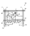
- FIG. 1 is a schematic diagram showing an exemplary configuration of an imaging device 100 according to the first embodiment.
- the imaging device 100 has a plurality of pixels 10 and peripheral circuits formed on a semiconductor substrate 60 .
- Each pixel 10 includes a photoelectric conversion unit 12.
- the photoelectric conversion unit 12 receives incident light and generates positive and negative charges. Positive and negative charges are typically hole-electron pairs.
- the photoelectric conversion part 12 is a photoelectric conversion structure including a photoelectric conversion layer arranged above the semiconductor substrate 60 .
- the photoelectric conversion unit 12 can be read as a photoelectric conversion structure.
- the photoelectric conversion unit 12 may be a photodiode formed on the semiconductor substrate 60 .
- the photoelectric conversion units 12 of each pixel 10 are shown spatially separated from each other. However, this is only for convenience of explanation.
- the photoelectric conversion units 12 of a plurality of pixels 10 may be continuously arranged on the semiconductor substrate 60 without spacing.
- pixels 10 are arranged in a plurality of rows and columns of m rows and n columns.
- m and n independently represent an integer of 1 or more.
- the pixels 10 form an imaging region R1 by being arranged two-dimensionally on the semiconductor substrate 60, for example.
- the number and arrangement of pixels 10 are not limited to the illustrated example.
- the center of each pixel 10 is positioned on a lattice point of a square lattice.
- a plurality of pixels 10 may be arranged such that the center of each pixel 10 is positioned on a lattice point such as a triangular lattice or a hexagonal lattice.
- the imaging device 100 may be used as a line sensor.
- the number of pixels 10 included in the imaging device 100 may be one.
- the peripheral circuits include a vertical scanning circuit 42 and a horizontal signal readout circuit 44.
- the peripheral circuitry may additionally include control circuitry 46 and voltage supply circuitry 48 .
- the peripheral circuit may further include a signal processing circuit, an output circuit, and the like.
- each circuit included in the peripheral circuit is provided on the semiconductor substrate 60 .
- part of the peripheral circuit may be arranged on another substrate different from the semiconductor substrate 60 on which the pixels 10 are formed.
- the vertical scanning circuit 42 is also called a row scanning circuit.
- the vertical scanning circuit 42 is connected to the address signal lines 34 provided for each row of the plurality of pixels 10 .
- the signal lines provided for each row of the plurality of pixels 10 are not limited to the address signal lines 34 .
- a plurality of types of signal lines can be connected to the vertical scanning circuit 42 for each row of the plurality of pixels 10 .
- the horizontal signal readout circuit 44 is also called a column scanning circuit.
- the horizontal signal readout circuit 44 is connected to the vertical signal lines 35 provided for each column of the plurality of pixels 10 .
- the control circuit 46 receives instruction data, clocks, etc. given from the outside of the imaging device 100 and controls the imaging device 100 as a whole. Typically, control circuit 46 has a timing generator. The control circuit 46 supplies drive signals to the vertical scanning circuit 42, the horizontal signal readout circuit 44, the voltage supply circuit 48, and the like. Arrows extending from the control circuit 46 in FIG. 1 schematically represent the flow of output signals from the control circuit 46 .
- Control circuitry 46 may be implemented by, for example, a microcontroller or one or more processors. A microcontroller may include one or more processors. The functions of the control circuit 46 may be realized by a combination of a general-purpose processing circuit and software, or by hardware specialized for such processing.
- a voltage supply circuit 48 supplies a predetermined voltage to each pixel 10 via the voltage line 38 .
- Voltage supply circuit 48 is not limited to a specific power supply circuit.
- the voltage supply circuit 48 may be a circuit that converts a voltage supplied from a power source such as a battery into a predetermined voltage, or may be a circuit that generates a predetermined voltage.
- the voltage supply circuit 48 may be part of the vertical scanning circuit 42 described above. As schematically shown in FIG. 1, these circuits forming a peripheral circuit are arranged in a peripheral region R2 outside the imaging region R1.
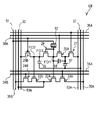
- FIG. 2 is a schematic diagram showing an exemplary circuit configuration of the pixel 10 of the imaging device 100 according to the first embodiment.
- one pixel 10A is shown as a representative to avoid complicating the drawing.
- Pixel 10A is an example of pixel 10 shown in FIG.
- the pixel 10A has a photoelectric conversion section 12 .
- the pixel 10A also includes a signal detection circuit electrically connected to the photoelectric conversion unit 12 .
- the photoelectric conversion section 12 includes a photoelectric conversion layer arranged above the semiconductor substrate 60 . That is, here, a stacked imaging device is exemplified as the imaging device 100 .
- the photoelectric conversion section 12 is supported by the semiconductor substrate 60 .
- the photoelectric converter 12 is connected to the accumulation control line 31 .
- a predetermined potential V ITO is applied to the accumulation control line 31 during operation of the imaging apparatus 100 .
- the potential V ITO applied to the accumulation control line 31 during operation of the imaging device 100 is, for example, , is a positive potential of about 10V.
- holes are used as signal charges will be exemplified below.
- the pixel 10A includes a first amplification transistor 22A, a first address transistor 24A, a first reset transistor 26A, a first transistor 29 which is a protection transistor, a second amplification transistor 22B, a second address transistor 24B, a second reset transistor 26B, and a capacitor. Includes element 30 .
- Transistors 22A, 24A, 26A, 29, 22B, 24B, and 26B are provided on semiconductor substrate 60 .
- the semiconductor substrate 60 is a silicon substrate.
- the transistors 22A, 24A, 26A, 29, 22B, 24B and 26B are field effect transistors (FET).
- FET field effect transistors
- the transistors 22A, 24A, 26A, 29, 22B, 24B and 26B are MOSFETs (Metal Oxide Semiconductor FETs).
- the first amplification transistor 22A, the first address transistor 24A, the first reset transistor 26A, the first transistor 29, the second amplification transistor 22B and the second address transistor 24B are N-type transistors.
- transistors 22A, 24A, 26A, 29, 22B and 24B are N-type MOSFETs or NMOS.
- the second reset transistor 26B is a P-type transistor.
- the second reset transistor 26B is a P-type MOSFET, that is, a PMOS.
- a gate electrode 22Ae of the first amplification transistor 22A is electrically connected to the photoelectric conversion section 12 .
- the charge accumulation node is a node electrically connected to the gate electrode 22Ae of the first amplification transistor 22A and the photoelectric conversion section 12 .
- the charge storage node partially includes an impurity region formed in semiconductor substrate 60 .
- the charge storage node has a function of temporarily holding charges generated by the photoelectric conversion unit 12 .
- a first charge storage portion FD1 as an example of a first impurity region, a second charge storage portion FD2 and a third charge storage portion FD3 as examples of a second impurity region are provided.
- the charge storage units FD1, FD2 and FD3 are included in the charge storage node.
- the charge storage units FD1, FD2, and FD3 have a function of temporarily retaining charges.
- the first charge storage unit FD1 is one of the source and drain of the first transistor 29, which is a protection transistor.
- the first charge storage unit FD1 is also one of the source and drain of the first reset transistor 26A.
- the third charge storage unit FD3 is the other of the source and drain of the first transistor 29 .
- the second charge storage unit FD2 is one of the source and drain of the second reset transistor 26B.
- the photoelectric conversion unit 12 When the photoelectric conversion unit 12 performs photoelectric conversion, charges generated by the photoelectric conversion flow to the first charge storage unit FD1, and charges are accumulated in the first charge storage unit FD1.
- the first charge storage unit FD1 is electrically connected to the gate electrode 29e of the first transistor 29, which is a protection transistor.
- the first transistor 29 When the potential of the first charge storage unit FD1 reaches the threshold potential VOF as the charge stored in the first charge storage unit FD1 increases, the first transistor 29 is turned on (turned on). As a result, the charge in the first charge storage unit FD1 flows to the second charge storage unit FD2, the third charge storage unit FD3, and the capacitive element 30.
- FIG. Note that the threshold potential V OF is a potential that depends on the threshold voltage of the first transistor 29 .
- threshold voltage refers to the gate-to-source voltage of a transistor when drain current begins to flow through the transistor.
- the capacitive element 30 is a metal-insulator-metal (MIM) capacitor.
- M metal-insulator-metal
- the “I” in MIM is an insulator, such as an oxide.
- MIM is a concept that includes MOM (Metal Oxide Metal).
- the MIM capacitor can realize a capacitive element 30 with a high capacity density. In particular, if an insulator with a high dielectric constant is used as the insulator, it is easy to realize the capacitive element 30 with a high capacitance density.
- One end of the capacitive element 30 is electrically connected to the second charge storage section FD2 and the third charge storage section FD3.
- the other end of the capacitive element 30 is electrically connected to the capacitive terminal line 37 .
- a potential V ss is applied to the other end of the capacitive element 30 via the capacitive terminal line 37 .
- the potential V ss is a fixed potential.
- One of the source and drain of the first amplification transistor 22A and one of the source and drain of the second amplification transistor 22B are connected to the power supply wiring 32 .
- a power supply potential V DD of about 3.3 V, for example, is supplied from the power supply wiring 32 to one of the drains.
- the other of the source and drain of the first amplification transistor 22A is connected to the first output line 35A via the first address transistor 24A.
- the other of the source and drain of the second amplification transistor 22B is connected to the second output line 35B via the second address transistor 24B.
- the vertical signal line 35 shown in FIG. 1 collectively describes the first output line 35A and the second output line 35B.
- a power supply potential V DD is supplied to one of the source and the drain of the first amplification transistor 22A.
- the first amplification transistor 22A outputs an electric signal corresponding to the potential of the first charge storage section FD1 to the first output line 35A via the first address transistor 24A.
- This electrical signal is specifically a voltage signal.
- a power supply potential V DD is supplied to one of the source and the drain of the second amplification transistor 22B.
- the second amplification transistor 22B outputs an electric signal corresponding to the potential of the second charge storage section FD2 to the second output line 35B via the second address transistor 24B.
- This electrical signal is specifically a voltage signal.
- a first address transistor 24A is connected between the first amplification transistor 22A and the first output line 35A.
- a first address line 34A is connected to the gate electrode 24Ae of the first address transistor 24A.
- a second address transistor 24B is connected between the second amplification transistor 22B and the second output line 35B.
- a second address line 34B is connected to the gate electrode 24Be of the second address transistor 24B.
- the address signal lines 34 shown in FIG. 1 collectively describe the first address lines 34A and the second address lines 34B.
- the vertical scanning circuit 42 applies to the first address line 34A a row selection signal that controls turning on and off of the first address transistor 24A. Thereby, the output of the first amplification transistor 22A of the selected pixel 10A can be read out to the first output line 35A.
- the vertical scanning circuit 42 applies a row selection signal to the second address line 34B to control ON and OFF of the second address transistor 24B. Thereby, the output of the second amplification transistor 22B of the selected pixel 10A can be read out to the second output line 35B.
- the arrangement of the first address transistor 24A and the arrangement of the second address transistor 24B are not limited to the example shown in FIG.
- the first address transistor 24A may be arranged between one of the source and drain of the first amplification transistor 22A and the power supply wiring 32 .
- the second address transistor 24B may be arranged between one of the source and drain of the second amplification transistor 22B and the power supply wiring 32 .
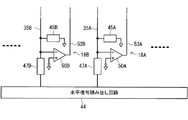
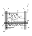
- FIG. 3 is a schematic diagram showing an exemplary circuit configuration after the pixel 10A.
- the first output line 35A is connected to the first load circuit 45A and the first column signal processing circuit 47A.
- the first load circuit 45A forms a source follower circuit together with the first amplification transistor 22A.
- the first column signal processing circuit 47A performs noise suppression signal processing, analog-digital conversion, and the like.
- the second output line 35B is connected to the second load circuit 45B and the second column signal processing circuit 47B.
- the second load circuit 45B forms a source follower circuit together with the second amplification transistor 22B.
- the second column signal processing circuit 47B performs noise suppression signal processing, analog-digital conversion, and the like.
- the column signal processing circuits 47A and 47B are also called row signal storage circuits.
- the noise suppression signal processing of the column signal processing circuits 47A and 47B is, for example, correlated double sampling.
- the column signal processing circuits 47A and 47B are connected to the horizontal signal readout circuit 44.
- the horizontal signal readout circuit 44 is connected to a first horizontal signal line and a second horizontal signal line (not shown).
- the horizontal signal readout circuit 44 reads signals from the first column signal processing circuit 47A to the first horizontal signal line, and reads signals from the second column signal processing circuit 47B to the second horizontal signal line. In this way, the signal that has passed through the first column signal processing circuit 47A and the signal that has passed through the second column signal processing circuit 47B can be read out in parallel. This is advantageous from the point of view of reading out these signals in a short time.
- a first load circuit 45A is provided for each column of a plurality of pixels 10A. The same applies to the second load circuit 45B, the first column signal processing circuit 47A and the second column signal processing circuit 47B. Load circuits 45A and 45B and column signal processing circuits 47A and 47B may be part of the peripheral circuits described above.
- a vertical scanning circuit 42 is connected to the gate electrode 26Ae of the first reset transistor 26A via the first reset line 36A.
- the first reset line 36A is provided for each row of the plurality of pixels 10A, like the first address line 34A and the second address line 34B.
- the vertical scanning circuit 42 can select the pixels 10A to be reset on a row-by-row basis by applying a row selection signal to the first address line 34A. By applying a reset signal to the gate electrode 26Ae of the selected row, the first reset transistor 26A of the selected row can be turned on. By turning on the first reset transistor 26A, the potential of the first charge storage section FD1 is reset.
- a vertical scanning circuit 42 is connected to the gate electrode 26Be of the second reset transistor 26B via a second reset line 36B.
- the second reset line 36B is provided for each row of the plurality of pixels 10A, like the first reset line 36A.
- the vertical scanning circuit 42 can select the pixels 10A to be reset on a row-by-row basis by applying a row selection signal to the second address line 34B.
- the second reset transistor 26B of the selected row can be turned on.
- the potential of the second charge storage section FD2 is reset.
- the potentials of the third charge storage section FD3 and the capacitive element 30 are reset along with the potential of the second charge storage section FD2.
- one of the drain and source of the first reset transistor 26A is the first charge storage unit FD1.
- the other of the drain and source of the first reset transistor 26A is electrically connected to the first feedback line 53A.
- the potential of the first feedback line 53A is supplied to the first charge storage section FD1 as the reset potential VRES for resetting the charge of the first charge storage section FD1.
- one of the drain and source of the second reset transistor 26B is the second charge storage unit FD2.
- the other of the drain and source of the second reset transistor 26B is electrically connected to the second feedback line 53B.
- the potential of the second feedback line 53B is supplied to the second charge storage section FD2 as the reset potential for resetting the charge of the second charge storage section FD2.
- the imaging device 100 has a first feedback circuit 16A including a first inverting amplifier 50A as part of the feedback path.
- the first feedback line 53A is connected to the output terminal of the first inverting amplifier 50A.
- the imaging device 100 has a second feedback circuit 16B including a second inverting amplifier 50B as part of the feedback path.
- the second feedback line 53B is connected to the output terminal of the second inverting amplifier 50B.
- the inverting input terminal of the first inverting amplifier 50A is connected to the first output line 35A.
- a first reference potential Vref1 is supplied to the non-inverting input terminal of the first inverting amplifier 50A when the imaging device 100 is in operation.
- the first reference potential Vref1 is, for example, a positive potential of 1V or around 1V.
- the formation of the feedback path resets the potential of the first charge storage unit FD1 to a potential that makes the potential of the first output line 35A equal to Vref1.
- Vref1 any potential magnitude within the range between the power supply potential VDD and the ground can be used.
- the inverting input terminal of the second inverting amplifier 50B is connected to the second output line 35B.
- a second reference potential Vref2 is supplied to the non-inverting input terminal of the second inverting amplifier 50B when the imaging device 100 is in operation.
- the second reference potential Vref2 is a positive potential higher than the first reference potential Vref2.
- the formation of the feedback path resets the potential of the second charge storage unit FD2 to a potential that makes the potential of the second output line 35B equal to Vref2.
- Vref2 a potential of any magnitude within the range of the power supply potential VDD and ground can be used.
- the first inverting amplifier 50A is provided for each column of the plurality of pixels 10A. The same applies to the second inverting amplifier 50B, the first feedback line 53A, the second feedback line 53B, the first feedback circuit 16A, and the second feedback circuit 16B. Inverting amplifiers 50A and 50B may be part of the peripheral circuitry described above.
- a column feedback circuit is configured in this embodiment. Feedback can suppress reset noise.
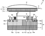
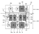
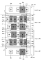
- FIG. 4 is a schematic plan view showing an example layout of each element in the pixel 10A according to the first embodiment.
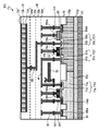
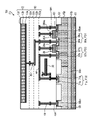
- FIG. 5 is a cross-sectional view schematically showing the arrangement of elements in the pixel 10A shown in FIG. If the pixel 10A is cut along the broken line VV in FIG. 4 and expanded, the cross section shown in FIG. 5 is obtained.
- the pixel 10A generally includes a semiconductor substrate 60, a photoelectric conversion section 12, and a conductive structure 89.
- the photoelectric conversion section 12 is arranged above the semiconductor substrate 60 .
- the photoelectric conversion section 12 is supported by the interlayer insulating layer 90 .
- An interlayer insulating layer 90 covers the semiconductor substrate 60 .
- Conductive structure 89 is disposed within interlayer insulating layer 90 .
- the interlayer insulating layer 90 includes multiple insulating layers.
- the multiple wiring layers include a first wiring layer and a second wiring layer.
- the first wiring layer includes address lines 34A and 34B, reset lines 36A and 36B, and the like.
- the second wiring layer includes output lines 35A and 35B, power supply wiring 32, feedback lines 53A and 53B, and the like.
- the number of insulating layers and the number of wiring layers in the interlayer insulating layer 90 are not limited to this example and can be set arbitrarily.
- the photoelectric conversion unit 12 converts incident light into electric charge.
- the photoelectric conversion section 12 includes a pixel electrode 12a, a counter electrode 12c, and a photoelectric conversion layer 12b.
- the pixel electrode 12 a is provided on the interlayer insulating layer 90 .
- the counter electrode 12c is arranged on the light incident side of the pixel electrode 12a.
- the photoelectric conversion layer 12b is arranged between these electrodes 12a and 12c.
- the photoelectric conversion layer 12b receives incident light through the counter electrode 12c and performs photoelectric conversion. Photoelectric conversion produces positive and negative charges.
- the photoelectric conversion layer 12b is typically provided continuously over a plurality of pixels 10A.
- the photoelectric conversion layer 12b is made of organic material or inorganic material. Amorphous silicon is exemplified as an inorganic material.
- the photoelectric conversion layer 12b may include a layer of organic material and a layer of inorganic material.
- the counter electrode 12c is provided over a plurality of pixels 10A, similar to the photoelectric conversion layer 12b.
- the counter electrode 12c is connected to the storage control line 31 described above.
- the potential of the storage control line 31 is controlled to make the potential of the counter electrode 12c higher than the potential of the pixel electrode 12a. This allows the pixel electrodes 12a to selectively collect the positive charges out of the positive and negative charges generated by photoelectric conversion.
- the counter electrode 12c is a translucent electrode.
- the counter electrode 12c is made of a transparent conductive material.
- ITO Indium Thin Oxide
- the term “translucent” in this specification means that at least a part of light having a wavelength that can be absorbed by the photoelectric conversion layer 12b is transmitted, and it is essential to transmit light over the entire wavelength range of visible light. is not.
- the pixel electrode 12a is spatially separated from the pixel electrode 12a of another adjacent pixel 10A. Thereby, the pixel electrode 12a is electrically isolated from the pixel electrodes 12a of the other pixels 10A.
- the pixel electrode 12a is made of metal or metal nitride. Aluminum, copper, etc. are illustrated as a metal.
- the pixel electrode 12a may be made of polysilicon or the like that is doped with an impurity to provide conductivity.
- the conductive structure 89 includes a plurality of wirings, plugs cp, contact plugs cpn and contact plugs cpp. One end of the conductive structure 89 is connected to the pixel electrode 12a. The other end of conductive structure 89 is connected to a circuit element formed on semiconductor substrate 60 . Thereby, the pixel electrode 12a of the photoelectric conversion section 12 and the circuit on the semiconductor substrate 60 are electrically connected to each other.
- multiple wirings and plugs cp are made of metal or metal compound. Copper, tungsten, etc. are illustrated as a metal. Examples of metal compounds include metal nitrides and metal oxides.
- Contact plugs cpn and cpp are made of polysilicon.
- the contact plug cpn is an N-type contact plug.
- the N-type contact plug cpn is doped with phosphorus, for example.
- the contact plug cpp is a P-type contact plug.
- the P-type contact plug cpp is doped with boron, for example.
- the contact plugs cpn and cpp have bar-shaped portions.
- the semiconductor substrate 60 includes a support substrate 61 and one or more semiconductor layers formed on the support substrate 61 .
- a silicon substrate specifically a P-type silicon substrate is exemplified.
- the semiconductor substrate 60 includes a P-type semiconductor region 61p, a first well region 65p that is a P-well region, a second well region 65n that is an N-well region, an impurity region 66n, an impurity region 67n, an impurity region 68an, An impurity region 68bn, an impurity region 71p, an impurity region 72ap and an element isolation region 69 are included.
- the P-type semiconductor region 61 p is arranged on the support substrate 61 .
- the P-type semiconductor region 61p contains P-type impurities at a lower concentration than the support substrate 61 does.
- the first well region 65p which is a P-well region, is a P-type impurity region.
- the first well region 65p is arranged on the P-type semiconductor region 61p.
- the first well region 65p contains P-type impurities. Specifically, the first well region 65p contains P-type impurities at a concentration lower than that of the support substrate 61 and higher than that of the P-type semiconductor region 61p.
- the second well region 65n which is an N-well region, is an N-type impurity region.
- the second well region 65n is arranged on the P-type semiconductor region 61p.
- the second well region 65n contains N-type impurities.
- the "NMOS Tr. region” is the region where the first well region 65p extends in plan view.
- the "PMOS Tr. region” is a region where the second well region 65n extends in plan view.
- an insulating layer 80 is provided on the semiconductor substrate 60 .
- the insulating layer 80 serves as the gate insulating film of the first amplification transistor 22A, the first address transistor 24A, the first reset transistor 26A, the first transistor 29, the second amplification transistor 22B, the second address transistor 24B, and the second reset transistor 26B.
- the first reset transistor 26A includes an impurity region 66n as one of its source and drain.
- the first reset transistor 26A includes an impurity region 68an as the other of the source and drain.
- the first reset transistor 26A includes an insulating layer 80 and a gate electrode 26Ae.
- the gate electrode 26Ae is provided on the insulating layer 80 .
- the first transistor 29, which is a protection transistor, includes an impurity region 66n as one of its source and drain.
- the first transistor 29 includes an impurity region 67n as the other of the source and drain.
- the first transistor 29 includes an insulating layer 80 and a gate electrode 29e. Gate electrode 29 e is provided on insulating layer 80 .
- the impurity region 66n is also the first charge storage unit FD1.
- the impurity region 67n is also the third charge storage unit FD3.
- the second reset transistor 26B includes an impurity region 71p as one of its source and drain.
- the second reset transistor 26B includes an impurity region 72ap as the other of the source and drain.
- the second reset transistor 26B includes an insulating layer 80 and a gate electrode 26Be.
- the gate electrode 26Be is provided on the insulating layer 80 .
- the impurity region 71p is also the second charge storage unit FD2.
- the impurity regions 66n, 67n, 68an and 68bn are N-type impurity regions.
- the impurity regions 71p and 72ap are P-type impurity regions.
- the impurity region 66n is arranged within the first well region 65p.
- the impurity region 66n includes a first region 66a and a second region 66b.
- the second region 66b is provided within the first region 66a.
- the second region 66b has a higher impurity concentration than the first region 66a.
- the impurity region 67n is arranged within the first well region 65p.
- the impurity region 67n includes a first region 67a and a second region 67b.
- the second region 67b is provided within the first region 67a.
- the second region 67b has a higher impurity concentration than the first region 67a.
- the impurity region 71p is arranged within the second well region 65n.
- the impurity region 71p includes a first region 71a and a second region 71b.
- the second region 71b is provided within the first region 71a.
- the second region 71b has a higher impurity concentration than the first region 71a.
- the impurity region 68an is arranged within the first well region 65p.
- Impurity region 68bn is arranged in second well region 65n.
- Impurity region 72ap is arranged in second well region 65n.
- the impurity region 68bn constitutes a well contact region of the second well region 65n. By applying a potential to impurity region 68bn, the potential of second well region 65n can be adjusted. Although not shown in FIG. 5, there is also an impurity region 68cp forming a well contact region of the first well region 65p. Impurity region 68cp is a P-type impurity region. By applying a potential to the impurity region 68cp, the potential of the first well region 65p can be adjusted.
- the impurity region 68an has a first region and a second region having a higher impurity concentration than the first region. This point also applies to the impurity regions 72ap, 68bn and 68cp.
- the first amplification transistor 22A, the first address transistor 24A, the first reset transistor 26A, the first transistor 29, the second amplification transistor 22B and the second address transistor 24B are NMOS.
- the second reset transistor 26B is a PMOS.
- the element isolation region 69 divides the second reset transistor 26B, which is a PMOS, into the first amplification transistor 22A, the first address transistor 24A, the first reset transistor 26A, the first transistor 29, the second amplification transistor 22B, and the second amplification transistor 22A, which are NMOS. It is electrically isolated from the address transistor 24B.
- the element isolation region 69 has a shallow trench isolation (STI) structure.
- An STI structure may be formed in the semiconductor substrate 60 by an STI process.
- the element isolation region 69 may be an implantation isolation region.
- the element isolation region 69 surrounds the first charge storage portion FD1 in plan view.
- the element isolation region 69 surrounds the second charge storage portion FD2 in plan view.
- the element isolation region 69 surrounds the third charge storage portion FD3 in plan view.
- the gate electrode 24Be of the 2-address transistor 24B is a gate electrode doped with an N-type impurity.
- the gate electrode 26Be of the second reset transistor 26B is a gate electrode doped with P-type impurities.
- the interlayer insulating layer 90 includes a plurality of insulating layers 90a, 90b, 90c and an insulating layer 90d.
- the number of insulating layers included in interlayer insulating layer 90 is not particularly limited.
- the plurality of plugs cp, the plurality of contact plugs cpn, and the plurality of contact plugs cpp are arranged in the insulating layer 90a.
- the plug cp, contact plug cpn and impurity region 68an are electrically connected in this order.
- the plug cp, contact plug cpp and impurity region 72ap are electrically connected in this order.
- the plug cp, contact plug cpn and impurity region 68bn are electrically connected in this order.
- the connection destination of these contact plugs cpn or cpp is the second impurity region.
- the plug cp, contact plug cpn, and gate electrode 26Ae are electrically connected in this order.
- the plug cp, contact plug cpn and gate electrode 29e are electrically connected in this order.
- the plug cp, contact plug cpp and gate electrode 26Be are electrically connected in this order.
- the pixel electrode 12a, plug cp, contact plug cpn, and impurity region 66n are electrically connected in this order. Therefore, the charge collected by the pixel electrode 12a is transmitted to the impurity region 66n through the plug cp and the contact plug cpn in this order.
- the connection destination of this contact plug cpn is the second region 66b of the impurity region 66n.
- the impurity region 67n, contact plug cpn, plug cp, wiring wr, plug cp, contact plug cpp, and impurity region 71p are electrically connected in this order.
- the second region 67b of the impurity region 67n, the contact plug cpn, the plug cp, the wiring wr, the plug cp, the contact plug cpp, and the second region 71b of the impurity region 71p are electrically connected in this order.
- the formation of a PN junction is avoided by interposing a metal or metal compound plug cp between contact plugs cpn and cpp of opposite conductivity types. It is also possible to directly connect the contact plugs cpn and cpp while avoiding the formation of the PN junction, for example, by siliciding the junctions of the contact plugs cpn and cpp.
- the insulating layer 80 is actually located under the gate electrodes of the transistors 22A, 24A, 26A, 29, 22B, 24B and 26B in the region on the semiconductor substrate 60. It is also provided in other areas. Specifically, the insulating layer 80 extends in the form of a film over the semiconductor substrate 60 in a region below the gate electrode and a region other than the region below the gate electrode.
- An insulating layer 85 is provided on the gate electrodes of the transistors 22A, 24A, 26A, 29, 22B, 24B and 26B. Specifically, the insulating layer 85 extends like a film over a portion of the insulating layer 80 that extends in a region other than under the gate electrode and over the gate electrode.
- the contact plug cpn is connected to the impurity region 68an through a contact hole.
- Contact plug cpp is connected to impurity region 72ap through a contact hole.
- Contact plug cpn is connected to impurity region 68bn through a contact hole.
- the contact plug cpn is connected to the gate electrode 26Ae through a contact hole.
- Contact plug cpn is connected to gate electrode 29e through a contact hole.
- the contact plug cpp is connected to the gate electrode 26Be through a contact hole.
- Contact plug cpn is connected to impurity region 66n through a contact hole.
- Contact plug cpn is connected to impurity region 67n through a contact hole.
- Contact plug cpp is connected to impurity region 71p through a contact hole.
- a contact plug cpn not drawn in FIG. 5 also exists.
- the contact plug cpn is connected to the gate electrode 22Ae of the first amplification transistor 22A through a contact hole.
- the contact plug cpn is connected to the gate electrode 22Be of the second amplification transistor 22B through a contact hole.
- the contact plug cpn is connected to the gate electrode 24Ae of the first address transistor 24A through a contact hole.
- the contact plug cpn is connected to the gate electrode 24Be of the second address transistor 24B through a contact hole.
- Each contact hole through which the contact plugs cpn or cpp connected to the impurity regions 68an, 72ap, 68bn, 66n, 67n and 71p pass is provided to penetrate the insulating layers 80 and 85 .
- Each contact hole through which the contact plug cpn or cpp connected to the gate electrodes 26Ae, 29e, 26Be, 22Ae, 22Be, 24Ae and 24Be passes is provided to penetrate the insulating layer 85 .
- FIG. 4 shows the first contact hole h1 through which the contact plug cpn connected to the impurity region 66n, that is, the first charge storage portion FD1 passes.
- a second contact hole h2 is shown through which the contact plug cpp connected to the impurity region 71p, that is, the second charge storage portion FD2 passes.
- a third contact hole h3 through which a contact plug cpn connected to the gate electrode 22Ae passes is shown.
- a fourth contact hole h4 through which a contact plug cpn connected to impurity region 68an passes is shown.
- a fifth contact hole h5 through which a contact plug cpn connected to the gate electrode 26Ae passes is shown.
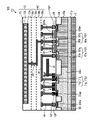
- FIG. 6 is a cross-sectional view schematically showing the structure of the first reset transistor 26A and its periphery according to the first embodiment.
- a first contact hole h1 through which a contact plug cpn connected to the impurity region 66n passes is provided to penetrate the insulating layers 80 and 85.
- a fourth contact hole h4 through which the contact plug cpn connected to the impurity region 68an passes is provided to penetrate the insulating layers 80 and 85 .
- Contact holes through which the contact plugs cpn or cpp connected to the impurity regions 72ap, 68bn, 67n and 71p pass are similarly provided to penetrate the insulating layers 80 and 85 .
- the fifth contact hole h5 through which the contact plug cpn connected to the gate electrode 26Ae passes is provided to penetrate the insulating layer 85.
- Contact holes through which contact plugs cpn or cpp connected to the gate electrodes 29e, 26Be, 22Ae, 22Be, 24Ae, and 24Be pass are similarly provided to penetrate the insulating layer 85.
- FIG. 7 is a cross-sectional view schematically showing the pixel 10A according to the first embodiment.
- the microlens 13 arranged on the photoelectric conversion section 12 is shown.
- illustration of the P-type semiconductor region 61p, the element isolation region 69, and the like is omitted.
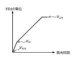
- FIG. 8 is a graph schematically showing the relationship between the exposure time of the imaging device 100 and the potential of the first charge storage section FD1 according to the first embodiment.
- impurity region 68cp constitutes a well contact region of first well region 65p.
- a first bias potential V sub is applied to the impurity region 68cp.
- the first bias potential V sub is, for example, 0V.
- impurity region 68bn constitutes a well contact region of second well region 65n.
- a second bias potential V NW is applied to the impurity region 68bn.
- the second bias potential V NW is, for example, 3.3V.
- the first charge accumulation unit FD1 during exposure of the imaging device 100 will be described with reference to FIG.
- the potential of the first charge storage section FD1 is reset to the reset potential VRES by a reset operation using the first reset transistor 26A. After that, as the exposure progresses, the charge accumulation in the first charge accumulation unit FD1 progresses, and the potential of the first charge accumulation unit FD1 rises.
- the first charge storage section FD1 When the potential of the first charge storage unit FD1 reaches the threshold potential V OF , the source-drain voltage of the first transistor 29, which is a protection transistor, becomes the threshold voltage, and the first transistor 29 is turned on. As a result, the first charge storage section FD1 is electrically connected to the second charge storage section FD2, the third charge storage section FD3, and the capacitive element 30, and accumulates charges in cooperation with them. In other words, the capacitance value of the charge storage node is larger after turn-on than before turn-on. Therefore, after turn-on, the slope of change in the potential of the first charge storage unit FD1 with respect to the exposure time is smaller than before turn-on.
- the potential of the first charge storage unit FD1 rises.
- the potential of the second charge storage section FD2 electrically connected to the first charge storage section FD1.
- V CLIP clipping potential
- a forward bias voltage is applied to the PN junction between the second charge storage section FD2 and the second well region 65n, which is the N well region.
- the charge is discharged from the second charge storage portion FD2 to the second well region 65n.
- the clipping potential V CLIP is a potential dependent on the second bias potential V NW .
- the relationship between the second bias potential V NW and the clipping potential V CLIP will be described.
- a PN junction is formed between the second well region 65n and the second charge storage section FD2.
- the clipping potential V CLIP deviates from the second bias potential V NW due to the built-in potential V bi of this PN junction.
- the built-in potential Vbi takes a value according to the impurity concentration of the second well region 65n and the impurity concentration of the second charge storage section FD2.
- the clipping potential V CLIP is the sum of the second bias potential V NW and the built-in potential V bi .
- the PN junction current that is, the current in the forward bias direction begins to flow when the potential of the second charge storage section FD2 becomes the potential near the second bias potential V NW due to the generation of charges, and then the current gradually increases. grow to Typically, the second bias potential V NW and the clipping potential V CLIP are approximately equal.
- the capacitance value of the charge accumulation node is small in a dark scene. Therefore, high-sensitivity imaging in a dark scene is possible.
- the capacitance value of the charge storage node is large. Therefore, highly saturated imaging is possible in a bright scene. For this reason, according to the present embodiment, the imaging apparatus 100 with a wide dynamic range can be realized.
- the reverse bias voltage applied to the PN junction between the first charge storage unit FD1 and the first well region 65p, which is the P well region, is applied to the charge storage unit FD1. smaller when is not progressing. Therefore, the leakage current of the first charge storage unit FD1 is smaller when the charge storage of the first charge storage unit FD1 is not progressing.
- This characteristic is advantageous from the viewpoint of performing high-sensitivity imaging in a dark scene. As a result, this characteristic can contribute to the realization of the imaging device 100 with a wide dynamic range.
- the potential of the first charge storage unit FD1 is prevented from changing beyond the limit potential V LIM . Together with the large capacitance value of the charge storage node in a bright scene, this makes it possible to realize the imaging device 100 that is less likely to fail even when a large amount of light is incident.
- the first transistor 29, which is a protective transistor When the first transistor 29, which is a protective transistor, is turned on, a channel through which charges pass is formed between the source and drain of the first transistor 29.
- the resistance of this channel may be referred to as channel resistance.
- the potential of the second charge storage unit FD2 can change with a delay with respect to the change of the potential of the first charge storage unit FD1.
- a difference can occur between the potential of the first charge storage unit FD1 and the potential of the second charge storage unit FD2 due to the presence of channel resistance and delay. Assuming that the channel resistance is zero, the potential of the first charge storage section FD1 and the potential of the second charge storage section FD2 can be treated as equal after a time sufficient for the RC time constant has passed.
- a difference due to channel resistance may occur between the limiting potential V LIM for the first charge storage section FD1 and the clipping potential V CLIP for the second charge storage section FD2. Considering the channel resistance to be zero, this difference can be treated as zero.
- the first transistor 29 corresponds to a protection transistor.
- the first well region 65p corresponds to the P well region.
- the second well region 65n corresponds to the N well region.
- the first impurity region corresponds to the first charge storage portion FD1.
- the second impurity region corresponds to the second charge accumulation portion FD2.
- the first conductivity type and the second conductivity type are different conductivity types. Specifically, the first conductivity type and the second conductivity type are conductivity types of opposite polarities.
- the first conductivity type is N type.
- the second conductivity type is P type.
- the first bias potential V sub and the second bias potential V NW are different potentials. It should be noted that the use of common reference numerals is not intended to limit the interpretation of this disclosure.
- imaging device 100 includes semiconductor substrate 60 .
- a semiconductor substrate 60 is provided with a first transistor 29 .
- the semiconductor substrate 60 has a first well region 65p, a second well region 65n, a first impurity region that is the first charge storage unit FD1, and a second impurity region that is the second charge storage unit FD2.
- the first well region 65p is a region of the second conductivity type.
- the second well region 65n is a first conductivity type region.
- the first impurity region is located within the first well region 65p.
- the first impurity region is one of the source and drain of the first transistor 29 .
- the first impurity region holds charges generated by photoelectric conversion.
- the first impurity region is electrically connected to the gate electrode 29 e of the first transistor 29 .
- the first impurity region is a first conductivity type impurity region.
- the second impurity region is located within the second well region 65n.
- the second impurity region is electrically connected to the other of the source and drain of the first transistor 29 .
- the second impurity region is of the second conductivity type.
- the first bias potential V sub is applied to the first well region 65p.
- a second bias potential V NW is applied to the second well region 65n.
- Application of the first bias potential V sub to the first well region 65p can stabilize the potential of the first well region 65p.
- Application of the second bias potential V NW to the second well region 65n can stabilize the potential of the second well region 65n. Further, by applying the second bias potential V NW to the second well region 65n, it is possible to adjust the potential when the change in the potential of the second impurity region due to the generation of charges by photoelectric conversion is stopped.
- the first transistor 29 is turned on when the potential of the first impurity region, which is the first charge storage section FD1, reaches the threshold potential VOF .
- the threshold potential V OF is greater than one of the first bias potential V sub and the second bias potential V NW and less than the other of the first bias potential V sub and the second bias potential V NW .
- the threshold potential V OF is greater than the first bias potential V sub and less than the second bias potential V NW .
- the threshold potential V OF may be smaller than the first bias potential V sub and larger than the second bias potential V NW .
- the potential of the second impurity region which is the second charge storage portion FD2
- the potential of the second impurity region can change as charges are generated. Then, when the potential of the second impurity region reaches a potential corresponding to the second bias potential V NW , the change in potential of the second impurity region can be stopped.
- a potential corresponding to the second bias potential V NW may be a clipping potential V CLIP .
- the first transistor 29 when the first transistor 29 is on, the first impurity region that is the first charge storage unit FD1 and the second impurity region that is the second charge storage unit FD2 are electrically connected.
- the second bias potential V NW By applying the second bias potential V NW to the second well region 65n, it is possible to adjust the potential when the change in the potential of the first impurity region due to the generation of charges by photoelectric conversion is stopped.
- the potential of the first impurity region can change as charges are generated. Then, when the potential of the first impurity region reaches a potential corresponding to the second bias potential V NW , the change in potential of the first impurity region can be stopped.
- the imaging device 100 includes an impurity region 68cp that is the first well contact region.
- the first well contact region is of the second conductivity type.
- the first well contact region is located within the first well region 65p.
- a first bias potential V sub is applied to the first well contact region.
- the first bias potential V sub can be applied to the first well region 65p through the first well contact region. By doing so, the potential of the first well region 65p can be stabilized.
- the imaging device 100 includes impurity regions 68bn that are second well contact regions.
- the second well contact region is of the first conductivity type.
- the second well contact region is located within the second well region 65n.
- a second bias potential V NW is applied to the second well contact region.
- the second bias potential V NW can be applied to the second well region 65n through the second well contact region.
- the potential of the second well region 65n can be stabilized.
- the potential when the change in potential of the second impurity region, which is the second charge storage unit FD2 associated with the generation of charges by photoelectric conversion, is stopped can be adjusted.
- the imaging device 100 includes a first contact plug that is a contact plug cpn, a first contact hole h1, a second contact plug that is a contact plug cpp, a second contact hole, a contact A third contact plug, which is a plug cpn, and a third contact hole h3 are provided.
- the semiconductor substrate 60 is provided with the first amplification transistor 22A.
- the first amplification transistor 22A outputs an electric signal corresponding to the potential of the first impurity region that is the first charge storage portion FD1.
- the source and drain of the first amplification transistor 22A are impurity regions of the first conductivity type and located in the first well region 65p.
- the first contact plug is connected to the first impurity region through the first contact hole.
- the second contact plug is connected to the second impurity region through the second contact hole.
- the third contact plug is connected to the gate electrode 22Ae of the first amplification transistor 22A through the third contact hole.
- the distance between the second well region 65n and the first contact hole h1 in plan view is defined as the distance L1.
- a distance between the first well region 65p and the second contact hole h2 in plan view is defined as a distance L2.
- a distance between the second well region 65n and the third contact hole h3 in plan view is defined as a distance L3.
- the symbol L3 and the corresponding arrow are shown at a position away from the third contact hole h3 for the sake of space. This point is the same for the code L6.
- a PN junction is formed between the first well region 65p and the second well region 65n.
- a distance L1 is a distance between this PN junction and the first contact hole h1 in plan view.
- a distance L2 is the distance between this PN junction and the second contact hole h2 in plan view.
- a distance L3 is the distance between this PN junction and the third contact hole h3 in plan view.
- the semiconductor substrate 60 is provided with an element isolation region 69 .
- the element isolation region 69 has an STI structure.
- the distance between the element isolation region 69 and the first contact hole h1 in plan view is defined as a distance L4.
- a distance between the element isolation region 69 and the second contact hole h2 in plan view is defined as a distance L5.
- a distance between the element isolation region 69 and the third contact hole h3 in plan view is defined as a distance L6.
- distance L1 is greater than distance L2.
- This configuration is rational from the viewpoint of realizing a compact imaging apparatus 100 with high image quality. Specifically, from the viewpoint of realizing a small pixel 10A, it is conceivable to reduce the sum of the distance L1 and the distance L2. On the other hand, from the viewpoint of suppressing leakage current originating from the second well region 65n in the first impurity region, which is the first charge storage portion FD1, it is conceivable to increase the distance L1. From the viewpoint of suppressing leakage current originating from the first well region 65p in the second impurity region, which is the second charge storage portion FD2, it is possible to increase the distance L2.
- the leak current in the second impurity region is reflected in the image quality when the first transistor 29 is on and the first impurity region and the second impurity region are electrically connected. At this time, since the capacitance value of the charge storage node is large, the influence of the leak current is less likely to appear on the image quality. Further, when the first transistor 29 is on, the charge is accumulated in the first impurity region to the extent that the shot noise becomes apparent, and the noise derived from the leak current of the second impurity region is hidden by the shot noise. can also be For these reasons, the leak current originating from the first well region 65p in the second impurity region has less influence on image quality than the leak current originating from the second well region 65n in the first impurity region. Considering the above, this configuration is rational from the viewpoint of realizing a compact imaging apparatus 100 with high image quality.
- distance L4 is greater than distance L5.
- This configuration is also rational from the viewpoint of realizing a compact imaging apparatus 100 with high image quality. By securing a distance from the STI structure in a plan view, it is possible to suppress leakage current resulting from a defective layer of the STI structure.
- distance L1 is greater than distance L3.
- This configuration is advantageous from the viewpoint of realizing the imaging device 100 with high image quality. Specifically, according to this configuration, it is easy to increase the distance L1. Therefore, it is easy to suppress the leakage current originating from the second well region 65n in the first impurity region, which is the first charge storage portion FD1. Specifically, it prevents impurities from the second well region 65n from diffusing into the first impurity region, and parasitic carriers generated in elements such as transistors in the second well region 65n from flowing into the first impurity region. easy to suppress.
- the distance L4 may be greater than the distance L6. This configuration is also advantageous from the viewpoint of realizing the imaging device 100 with high image quality.
- FIG. 9 is a schematic plan view showing an example layout of elements in two pixels 10A adjacent to each other.
- One of the two pixels 10A is the first pixel 10A1 and the other is the second pixel 10A2.
- the first pixel 10A1 and the second pixel 10A2 respectively include the first well region 65p, the second well region 65n, the first transistor 29, the second impurity region that is the second charge storage unit FD2, and the contact It has a first contact plug that is a plug cpn, a first contact hole h1, a third contact plug that is a contact plug cpn, a third contact hole h3, and a first amplification transistor 22A.
- the second well region 65n of the first pixel 10A1, the first well region 65p of the first pixel 10A1, the first The well region 65p and the second well region 65n of the second pixel 10A2 are arranged in this order.
- This configuration is advantageous from the viewpoint of realizing the imaging device 100 with high image quality. Specifically, according to this configuration, it is easy to secure the distance between the first impurity region, which is the first charge storage unit FD1 of the first pixel 10A1, and the second well region 65n of the second pixel 10A2. Therefore, this configuration is advantageous from the viewpoint of suppressing leakage current originating from the second well region 65n of the second pixel 10A2 in the first impurity region of the first pixel 10A1. Further, according to this configuration, it is easy to secure the distance between the first impurity region of the second pixel 10A2 and the second well region 65n of the first pixel 10A1. Therefore, this configuration is advantageous from the viewpoint of suppressing leakage current from the second well region 65n of the first pixel 10A1 in the first impurity region of the second pixel 10A2.
- the second pixel 10A2 is obtained by flipping the first pixel 10A1.
- a first pixel 10A1 in FIG. 9 corresponds to the pixel 10A in FIG.
- a second pixel 10A2 in FIG. 9 corresponds to the flipped version of the pixel 10A in FIG.
- imaging device 100 includes capacitive element 30 .
- the capacitive element 30 is electrically connected to the second impurity region, which is the second charge storage section FD2. This configuration is suitable for realizing the imaging device 100 with a wide dynamic range.
- the capacitive element 30 is an MIM capacitor. This configuration is suitable for realizing the imaging device 100 with a wide dynamic range.
- the capacitive element 30 may overlap with at least one selected from the group consisting of the first contact hole h1 and the second contact hole h2.
- the capacitive element 30 according to this configuration suppresses light incidence on at least one selected from the group consisting of the first impurity region that is the first charge storage unit FD1 and the second impurity region that is the second charge storage unit FD2. I can. Therefore, this configuration is advantageous from the viewpoint of realizing the imaging device 100 with high image quality.
- the capacitive element 30 is arranged on the insulating layer 90a.
- the capacitive element 30 can be arranged in at least one layer selected from the insulating layers 90a to 90d.
- the capacitive element 30 contains a metal or a metal compound, the light incidence suppressing effect described above is likely to appear.
- the case where the capacitive element 30 is an MIM capacitor corresponds to such a case.
- the capacitive element 30 overlaps both the first contact hole h1 and the second contact hole h2 in plan view. According to the first example, light incidence on both the first impurity region that is the first charge storage unit FD1 and the second impurity region that is the second charge storage unit FD2 can be suppressed. However, in plan view, the capacitive element 30 may overlap only one of the first contact hole h1 and the second contact hole h2. In the second example, in plan view, the capacitive element 30 overlaps the first contact hole h1, but does not overlap the second contact hole h2. As can be understood from the above description, the leak current in the first impurity region is more likely to affect image quality than the leak current in the second impurity region.
- the capacitive element 30 when there is a constraint such as a limited space for arranging the capacitive element 30, it is possible to suppress the influence of the leak current on the image quality while satisfying the constraint.
- a third example in which the capacitive element 30 does not overlap the first contact hole h1 but overlaps the second contact hole h2 in plan view can also be adopted.
- the imaging device 100 includes a first reset transistor 26A.
- the first reset transistor 26A resets the potential of the first impurity region, which is the first charge storage section FD1, to the reset potential VRES .
- the first transistor 29 is turned on when the potential of the first impurity region reaches the threshold potential VOF .
- a second bias potential V NW is applied to the second well region 65n. When the potential of the first impurity region reaches a potential corresponding to the second bias potential V NW , the potential of the first impurity region stops changing.
- the difference between the reset potential VRES and the threshold potential VOF may be smaller than the difference between the threshold potential VOF and the second bias potential VNW .
- This configuration is suitable for realizing the imaging device 100 with a wide dynamic range. Specifically, typically, the low light amount region in which high sensitivity should be emphasized is not so wide. According to this configuration, by appropriately narrowing the low-light-intensity region where the first transistor 29 is off and high sensitivity is important, the light-intensity region in which the first transistor 29 is on can be widened. Thereby, the saturation level of the imaging device 100 can be increased. Thereby, the imaging device 100 with a wide dynamic range can be realized.
- the difference between the reset potential VRES and the threshold potential VOF may be 30% or less of the difference between the threshold potential VOF and the second bias potential VNW .
- the difference between the reset potential VRES and the threshold potential VOF may be greater than 10% of the difference between the threshold potential VOF and the second bias potential VNW .
- This configuration is suitable for avoiding a situation in which the image quality of the imaging device 100 deteriorates due to noise derived from the second impurity region, which is the second charge storage section FD2.
- the reverse bias voltage applied to the PN junction between the second impurity region and the second well 65n is set to as big as Therefore, the leak current in the second impurity region is larger when the charge accumulation in the second impurity region is not progressing. Therefore, it is immediately after the first transistor 29 is turned on that the leakage current of the second impurity region is likely to be reflected in the image quality.
- the first transistor 29 when the first transistor 29 is turned on, the charge to the extent that the shot noise becomes apparent is accumulated in the first impurity region, which is the first charge accumulation unit FD1, and the shot noise causes the first impurity region to appear.
- the noise derived from the leak current of the second impurity region, which is the second charge storage section FD2 is likely to be hidden.
- the difference between the reset potential VRES and the threshold potential VOF may be greater than 12% of the difference between the threshold potential VOF and the second bias potential VNW .
- the reset potential V RES is 0V.
- the threshold potential V OF is 0.5V.
- the second bias potential V NW is 3.3V.
- the difference between the reset potential VRES and the threshold potential VOF is about 18% of the difference between the threshold potential VOF and the second bias potential VNW .
- the adjustment of the threshold potential V OF can be performed through adjustment of the threshold voltage of the first transistor 29, adjustment of the reset potential of the second impurity region which is the second charge storage section FD2, and the like.
- imaging device 100 includes photoelectric conversion unit 12 .
- the photoelectric conversion section 12 has a counter electrode 12c, a pixel electrode 12a, and a photoelectric conversion layer 12b.
- the photoelectric conversion layer 12b is arranged between the counter electrode 12c and the pixel electrode 12a.
- the photoelectric conversion layer 12b generates electric charges. Charges are led from the pixel electrode 12a to the first impurity region, which is the first charge accumulation portion FD1.
- the imaging device 100 includes a first pixel 10A.
- the first pixel 10A has a photoelectric conversion unit 12, a first transistor 29, a second impurity region that is the second charge storage unit FD2, a first well region 65p and a second well region 65n.
- the number of pixel electrodes 12a in the first pixel 10A is one.
- This configuration is suitable for realizing a fine imaging device 100 .
- a plurality of pixel electrodes exist in one pixel it is difficult to reduce the size of the image pickup device while avoiding deterioration of the characteristics of the image pickup device.
- a relatively large pixel electrode is provided in a high-sensitivity cell
- a relatively small pixel electrode is provided in a high-saturation cell
- the size ratio of the pixel electrodes produces a sensitivity ratio.
- the number of pixel electrodes 12a in the first pixel 10A is one. This configuration alleviates the difficulty of processing and miniaturizing the pixel electrode 12a, and makes it possible to miniaturize the imaging device 100 without manifesting deterioration of the characteristics of the imaging device 100 such as sensitivity at low light intensity. .
- imaging device 100 includes microlens 13 and photoelectric conversion unit 12 . Light enters the photoelectric conversion unit 12 through the microlens 13 .
- the photoelectric conversion unit 12 generates electric charges.
- the imaging device 100 includes a first pixel 10A.
- the first pixel 10A has a microlens 13, a photoelectric conversion section 12, a first transistor 29, a second impurity region which is the second charge storage section FD2, a first well region 65p and a second well region 65n.
- the number of convex surfaces of the microlens 13 in the first pixel 10A is one. This configuration is suitable for realizing a fine imaging device 100 .
- the convex surface of the microlens is made relatively large in the high-sensitivity cell
- the convex surface of the microlens is made relatively small in the high-saturation cell
- the sensitivity ratio is adjusted by the size ratio of the convex surface.
- the number of pixel electrodes 12a in the first pixel 10A is one. This configuration alleviates the difficulty of microlens processing and miniaturization, and makes it possible to reduce the size of the imaging device 100 without manifesting deterioration of the characteristics such as the oblique incidence characteristics of the imaging device 100 .
- the method for driving imaging device 100 includes a first step, a second step, and a third step.
- the first step is the step of increasing the reverse bias voltage applied to the first PN junction due to accumulation of charges generated by photoelectric conversion when the first transistor 29 is off.
- the second step is to turn on the first transistor 29 in response to charge accumulation.
- the third step is that when the first transistor 29 is on, the accumulation of charge causes the reverse bias voltage applied to the second PN junction to decrease, leading to the forward bias voltage being applied to the second PN junction, This is a step in which electric charges are discharged.
- This configuration is suitable for realizing the imaging apparatus 100 that is hard to fail even when a large amount of light is incident and has a wide dynamic range.
- the first step when the first transistor 29 is off, electric charge is generated by photoelectric conversion in the imaging device 100, and the electric charge is accumulated in a region partitioned by the first transistor 29 in the imaging device 100. This increases the reverse bias voltage applied to the first PN junction.
- the first transistor 29 is turned on when the source-drain voltage of the first transistor 29 reaches the threshold voltage by accumulating charges in the partitioned region.
- the third step when the first transistor 29 is on, charge is accumulated in the region across the first transistor 29 in the imaging device 100, thereby reducing the reverse bias voltage applied to the second PN junction. As a result, a forward bias voltage is applied to the second PN junction, thereby discharging the charge.
- the first PN junction can be the PN junction between the first impurity region, which is the first charge storage unit FD1, and the first well region 65p.
- the second PN junction may be a PN junction between the second impurity region, which is the second charge storage unit FD2, and the second well region 65n.
- FIG. 10 is a schematic plan view showing an example layout of elements in a pixel 10B according to the second embodiment.
- the element isolation region 69 extends like a strip along the PN junction between the first well region 65p and the second well region 65n.
- the element isolation region 69 has an STI structure.
- a PN junction can be formed between the element isolation region 69 and the support substrate 61 in the thickness direction of the semiconductor substrate 60 .
- the magnitude relationship of distance L1>distance L2 when the magnitude relationship of distance L4>distance L5 is also likely to be established.
- the magnitude relationship of distance L4>distance L6 is also likely to be established.
- FIG. 11 is a schematic plan view showing an example layout of elements in two pixels 10B adjacent to each other.
- One of the two pixels 10B is the first pixel 10B1 and the other is the second pixel 10B2.
- the first pixel 10B1 and the second pixel 10B2 respectively include a first well region 65p, a second well region 65n, a first transistor 29, a second impurity region that is the second charge storage unit FD2, and a contact. It has a first contact plug that is a plug cpn, a first contact hole h1, a third contact plug that is a contact plug cpn, a third contact hole h3, and a first amplification transistor 22A.
- the second well region 65n of the first pixel 10B1, the first well region 65p of the first pixel 10B1, the first well region 65p of the second pixel 10B2, and the first well region 65p of the second pixel 10B2 are sequentially arranged along the direction from the first pixel 10B1 to the second pixel 10B2.
- the well region 65p and the second well region 65n of the second pixel 10B2 are arranged in this order.
- the second pixel 10B2 is obtained by flipping the first pixel 10B1.
- a first pixel 10B1 in FIG. 11 corresponds to the pixel 10B in FIG.
- a second pixel 10B2 in FIG. 10 corresponds to the flipped pixel 10B in FIG.
- FIG. 12 is a cross-sectional view schematically showing the configuration of a pixel 10C according to the third embodiment.
- the gate electrode 29e of the first transistor 29, which is a protection transistor is a gate electrode doped with P-type impurities. According to this configuration, even if the channel dose of the first transistor 29 is suppressed, the threshold voltage of the first transistor 29 can be ensured due to the contribution of the work function of the gate electrode 29e. By suppressing the channel dose, it is possible to reduce the PN junction electric field intensity around the first charge storage portion FD1 and the third charge storage portion FD3 formed in the first well region 65p, thereby suppressing leakage current. can.
- the gate electrode 29e of the first transistor 29 is connected to the contact plug cpp. Specifically, the contact plug cpp is connected to the gate electrode 29e through a contact hole.
- the term "first transistor 29" will be used below to further describe the present embodiment.
- the first transistor 29 corresponds to a protection transistor.
- the conductivity type of the gate electrode 29 e of the first transistor 29 is opposite to the conductivity type of the source and drain of the first transistor 29 . According to this configuration, leakage current can be easily suppressed.
- FIG. 13 is a cross-sectional view schematically showing the configuration of a pixel 10D according to the fourth embodiment.
- the imaging device 100 has contact plugs cgn and cgp instead of the contact plugs cpn and cpp.
- the contact plugs cgn and cgp are common to the gate electrodes 22Ae, 24Ae, 26Ae, 29e, 22Be, 24Be and 26Be in that they have a film shape portion.
- the contact plugs cgn and cgp are common to the gate electrodes 22Ae, 24Ae, 26Ae, 29e, 22Be, 24Be and 26Be in that they are made of polysilicon.
- contact plugs cgn and cgp and the gate electrodes 22Ae, 24Ae, 26Ae, 29e, 22Be, 24Be and 26Be can be formed by a common film formation process. This is advantageous from the viewpoint of simplification of the manufacturing process.
- the contact plugs cgn and cgp in the fourth embodiment can also be called gate polysilicon pads.
- the heights of the contact plugs cgn and cgp and the heights of the gate electrodes 22Ae, 24Ae, 26Ae, 29e, 22Be, 24Be and 26Be are the same.
- a plug cp is connected to each of these elements aligned in height. This is also advantageous from the viewpoint of simplification of the manufacturing process.
- FIG. 14 is a cross-sectional view schematically showing the configuration of a pixel 10E according to the fifth embodiment.
- the imaging device 100 according to the fifth embodiment includes the gate electrode 29e doped with the P-type impurity described in the third embodiment, and the contact plugs cgn and cgp described in the fourth embodiment.
- FIG. 15 is a schematic diagram showing an exemplary circuit configuration of the pixel 10F of the imaging device according to the sixth embodiment.
- the pixel 10F comprises a feedback transistor 27.
- a column feedback circuit using feedback transistors 27 is configured.
- the pixel 10F includes a capacitive element 17 and a capacitive element 18 .
- the feedback transistor 27 is an N-type transistor. Specifically, feedback transistor 27 is an NMOS. Capacitive element 17 and capacitive element 18 are, for example, MIM capacitors.
- One end of the capacitive element 18 is electrically connected to the first charge storage section FD1.
- the other end of the capacitive element 18 is electrically connected to one of the source and drain of the feedback transistor 27 and one end of the capacitive element 17 .
- the other end of the capacitive element 17 is electrically connected to the capacitive terminal line 37 .
- the other of the source and drain of the feedback transistor 27 is electrically connected to the first feedback line 53A.
- First charge storage unit FD1 First charge storage unit FD1, first amplification transistor 22A, first address transistor 24A, first output line 35A, first inverting amplifier 50A, first feedback line 53A, feedback transistor 27, capacitive element 18, and first charge storage unit FD1 are connected in this order. With this connection, a signal derived from the potential of the first charge storage unit FD1 can be negatively fed back to the first charge storage unit FD1.
- One of the source and drain of the second reset transistor 26B is the second charge storage unit FD2.
- the other of the source and drain of the second reset transistor 26B is electrically connected to the second feedback line 53B.
- the second charge storage section FD2 The second charge storage section FD2, the second amplification transistor 22B, the second address transistor 24B, the second output line 35B, the second inverting amplifier 50B, the second feedback line 53B, the other of the source and the drain of the second reset transistor 26B and the second
- the two charge storage units FD2 are connected in this order. Due to this connection, a signal derived from the potential of the second charge storage section FD2 can be negatively fed back to the second charge storage section FD2.
- FIG. 16 is a schematic diagram showing an exemplary circuit configuration of the pixel 10G of the imaging device according to the seventh embodiment.
- an intra-pixel feedback circuit is constructed instead of the column feedback circuit using the inverting amplifiers 50A and 50B.
- One end of the capacitive element 18 is electrically connected to the first charge storage section FD1.
- the other end of the capacitive element 18 is electrically connected to one of the source and drain of the feedback transistor 27 and one end of the capacitive element 17 .
- the other end of the capacitive element 17 is electrically connected to the capacitive terminal line 37 .
- One of the source and drain of the first amplification transistor 22A is electrically connected to the power supply wiring 32 .
- the other of the source and drain of the first amplification transistor 22A and the one of the source and drain of the first address transistor 24A are electrically connected to the other of the source and drain of the feedback transistor 27 .
- the first charge storage section FD1, the first amplification transistor 22A, the feedback transistor 27, the capacitive element 18, and the first charge storage section FD1 are connected in this order. With this connection, a signal derived from the potential of the first charge storage unit FD1 can be negatively fed back to the first charge storage unit FD1.
- One of the source and drain of the second reset transistor 26B is the second charge storage unit FD2.
- One of the source and drain of the second amplification transistor 22B is electrically connected to the power supply wiring 32 .
- the other of the source and drain of the second amplification transistor 22B and one of the source and drain of the second address transistor 24B are electrically connected to the other of the source and drain of the second reset transistor 26B.
- the second charge storage section FD2 the other of the sources and drains of the second amplification transistor 22B and the second reset transistor 26B, and the second charge storage section FD2 are connected in this order. Due to this connection, a signal derived from the potential of the second charge storage section FD2 can be negatively fed back to the second charge storage section FD2.
- FIG. 17 is a schematic diagram showing an exemplary circuit configuration of the pixel 10H of the imaging device 100 according to the eighth embodiment.
- FIG. 18 is a schematic plan view showing an example layout of elements in a pixel 10H according to the eighth embodiment.
- FIG. 19 is a cross-sectional view schematically showing the arrangement of each element in the pixel 10H shown in FIG. 18. As shown in FIG. If the pixel 10H is cut along the broken line XIX-XIX in FIG. 18 and developed, the cross section shown in FIG. 19 is obtained.
- the second reset transistor 26B is an N-type transistor. Specifically, the second reset transistor 26B in the eighth embodiment is an NMOS. The second reset transistor 26B is provided in the first well region 65p.
- the first charge storage unit FD1 is one of the source and drain of the first transistor 29, which is a protection transistor.
- the first charge storage unit FD1 is also one of the source and drain of the first reset transistor 26A.
- the third charge storage unit FD3 is the other of the source and drain of the first transistor 29 .
- the third charge storage unit FD3 is also one of the source and drain of the second reset transistor 26B.
- the second charge storage unit FD2 is different from the source and the drain of the second reset transistor 26B.
- the second charge storage portion FD2 is the impurity region 71p. Note that in FIG. 19, the impurity region 73n is the other of the source and drain of the second reset transistor 26B. Impurity region 73n is an N-type impurity region.
- the second well region 65n within the pixel 10H can be made smaller. This is advantageous from the viewpoint of reducing the size of the pixel 10H. Further, according to the eighth embodiment, all transistors in the pixel 10H can be NMOS. This is advantageous from the viewpoint of simplifying the manufacturing process of the imaging device.
- FIG. 20 is a schematic diagram showing an exemplary circuit configuration of the pixel 10I of the imaging device 100 according to the ninth embodiment.
- FIG. 21 is a schematic plan view showing an example layout of each element in the pixel 10I according to the ninth embodiment.
- FIG. 22 is a cross-sectional view schematically showing the arrangement of elements in the pixel 10I shown in FIG. If the pixel 10I is cut along the dashed line XXII-XXII in FIG. 21 and developed, the cross section shown in FIG. 22 is obtained.
- the second reset transistor 26B is not provided.
- the second charge storage portion FD2 is the impurity region 71p.
- the imaging device has well reset lines 39 .
- a potential is applied to the second well region 65n via the well reset line 39.
- FIG. This application can reset the potential of the second charge storage unit FD2.
- the well reset line 39 applies a potential to the second well region 65n via the plug cp, contact plug cpn and impurity region 68bn in this order.
- the second well region 65n in the pixel 10I can be made smaller. This is advantageous from the viewpoint of reducing the size of the pixel 10I.
- the absence of the second reset transistor 26B is also advantageous from the viewpoint of reducing the size of the pixel 10I.
- all the transistors in the pixel 10I can be NMOS. This is advantageous from the viewpoint of simplifying the manufacturing process of the imaging device.
- the plug cp and the gate electrode 26Be are connected via the contact plug cpp.
- Plug cp and gate electrode 29e are connected via contact plug cpn.
- plug cp and gate electrode 26Be may be directly connected.
- Plug cp and gate electrode 29e may be directly connected.
- the plug cp and the gate electrode 29e are connected via the contact plug cpp.
- plug cp and gate electrode 29e may be directly connected.
- the connection between the plug cp and another gate electrode may be made indirectly through the contact plug cpn or cpp, or may be made directly.
- the imaging device of the present disclosure is useful, for example, for image sensors, digital cameras, and the like.
- the imaging device of the present disclosure can be used for medical cameras, robot cameras, security cameras, cameras mounted on vehicles, and the like.
Abstract
An imaging device comprising a semiconductor substrate and a first transistor provided in the semiconductor substrate and having a first gate electrode, a source, and a drain. The semiconductor substrate comprises: a first well region of a second conductivity type; a second well region of a first conductivity type different from the second conductivity type; a first impurity region of the first conductivity type which is positioned in the first well region, is one of the source and the drain, holds charge generated by photoelectric conversion, and is electrically connected to the first gate electrode; and a second impurity region of the second conductivity type positioned in the second well region and electrically connected to the other of the source and the drain.
Description
本開示は、撮像装置及びその駆動方法に関する。
The present disclosure relates to an imaging device and its driving method.
デジタルカメラ等にCCD(Charge Coupled Device)イメージセンサ及びCMOS(Complementary Metal Oxide Semiconductor)イメージセンサが広く用いられている。これらのイメージセンサは、半導体基板に形成されたフォトダイオードを有する。
CCD (Charge Coupled Device) image sensors and CMOS (Complementary Metal Oxide Semiconductor) image sensors are widely used in digital cameras and the like. These image sensors have photodiodes formed in a semiconductor substrate.
フォトダイオードに代えて、半導体基板の上方に光電変換層を配置した構造も提案されている。このような構造を有する撮像装置は、積層型の撮像装置と呼ばれることがある。積層型の撮像装置では、光電変換によって生成された電荷が、半導体基板に形成された不純物領域等に信号電荷として一時的に蓄積される。その後、蓄積された電荷量に応じた信号が、半導体基板に形成されたCCD回路又はCMOS回路を介して読み出される。
A structure in which a photoelectric conversion layer is arranged above a semiconductor substrate instead of a photodiode has also been proposed. An imaging device having such a structure is sometimes called a stacked imaging device. In the stacked imaging device, charges generated by photoelectric conversion are temporarily accumulated as signal charges in an impurity region or the like formed in a semiconductor substrate. After that, a signal corresponding to the accumulated charge amount is read out through a CCD circuit or a CMOS circuit formed on the semiconductor substrate.
特許文献1から3には、撮像装置の一例が記載されている。
Examples of imaging devices are described in Patent Documents 1 to 3.
本開示は、大光量が入射しても故障し難くかつ広いダイナミックレンジを有する撮像装置を実現することに適した技術を提供する。
The present disclosure provides a technique suitable for realizing an imaging device that is hard to break down even when a large amount of light is incident and has a wide dynamic range.
本開示の一態様に係る撮像装置は、
半導体基板と、
前記半導体基板に設けられ、第1ゲート電極、ソース及びドレインを有する第1トランジスタと、を備え、
前記半導体基板は、
第2導電型の第1ウェル領域と、
前記第2導電型とは異なる第1導電型の第2ウェル領域と、
前記第1ウェル領域内に位置し、前記ソース及び前記ドレインの一方であり、光電変換により生成された電荷を保持し、前記第1ゲート電極に電気的に接続された、前記第1導電型の第1不純物領域と、
前記第2ウェル領域内に位置し、前記ソース及び前記ドレインの他方に電気的に接続された、前記第2導電型の第2不純物領域と、を含む。 An imaging device according to an aspect of the present disclosure includes:
a semiconductor substrate;
a first transistor provided on the semiconductor substrate and having a first gate electrode, a source and a drain;
The semiconductor substrate is
a first well region of a second conductivity type;
a second well region of a first conductivity type different from the second conductivity type;
the first conductivity type located in the first well region, being one of the source and the drain, holding charges generated by photoelectric conversion, and electrically connected to the first gate electrode; a first impurity region;
a second impurity region of the second conductivity type located in the second well region and electrically connected to the other of the source and the drain.
本開示に係る技術は、大光量が入射しても故障し難くかつ広いダイナミックレンジを有する撮像装置を実現することに適している。
The technology according to the present disclosure is suitable for realizing an imaging device that is hard to break down even when a large amount of light is incident and has a wide dynamic range.
(本開示に係る一態様の概要)
本開示の第1態様に係る撮像装置は、
半導体基板と、
前記半導体基板に設けられ、第1ゲート電極、ソース及びドレインを有する第1トランジスタと、を備える。前記半導体基板は、
第2導電型の第1ウェル領域と、
前記第2導電型とは異なる第1導電型の第2ウェル領域と、
前記第1ウェル領域内に位置し、前記ソース及び前記ドレインの一方であり、光電変換により生成された電荷を保持し、前記第1ゲート電極に電気的に接続された、前記第1導電型の第1不純物領域と、
前記第2ウェル領域内に位置し、前記ソース及び前記ドレインの他方に電気的に接続された、前記第2導電型の第2不純物領域と、を含む。 (Overview of one aspect of the present disclosure)
An imaging device according to a first aspect of the present disclosure includes:
a semiconductor substrate;
a first transistor provided on the semiconductor substrate and having a first gate electrode, a source and a drain. The semiconductor substrate is
a first well region of a second conductivity type;
a second well region of a first conductivity type different from the second conductivity type;
the first conductivity type located in the first well region, being one of the source and the drain, holding charges generated by photoelectric conversion, and electrically connected to the first gate electrode; a first impurity region;
a second impurity region of the second conductivity type located in the second well region and electrically connected to the other of the source and the drain.
第1態様に係る技術は、大光量が入射しても故障し難くかつ広いダイナミックレンジを有する撮像装置を実現することに適している。
The technology according to the first aspect is suitable for realizing an imaging device that is unlikely to break down even when a large amount of light is incident and has a wide dynamic range.
本開示の第2態様において、例えば、第1態様に係る撮像装置では、
前記第1ウェル領域には、第1バイアス電位が印加されてもよく、
前記第2ウェル領域には、前記第1バイアス電位と異なる第2バイアス電位が印加されてもよい。 In the second aspect of the present disclosure, for example, in the imaging device according to the first aspect,
A first bias potential may be applied to the first well region,
A second bias potential different from the first bias potential may be applied to the second well region.
第2態様の構成は、撮像装置の構成の具体例である。
The configuration of the second aspect is a specific example of the configuration of the imaging device.
本開示の第3態様において、例えば、第2態様に係る撮像装置では、
前記第2不純物領域の電位は、前記電荷の生成に伴って変化し、
前記電荷の前記生成に伴う前記第2不純物領域の前記電位の変化は、前記第2バイアス電位に応じた電位で停止してもよい。 In the third aspect of the present disclosure, for example, in the imaging device according to the second aspect,
the potential of the second impurity region changes with the generation of the charge,
The change in the potential of the second impurity region accompanying the generation of the charge may stop at a potential corresponding to the second bias potential.
第3態様の構成は、撮像装置の構成の具体例である。
The configuration of the third aspect is a specific example of the configuration of the imaging device.
本開示の第4態様において、例えば、第1態様から第3態様のいずれか1つに係る撮像装置は、第1コンタクトプラグ、第1コンタクトホール、第2コンタクトプラグ及び第2コンタクトホールをさらに備えていてもよく、
前記第1コンタクトプラグは、前記第1コンタクトホールを通って前記第1不純物領域に接続されていてもよく、
前記第2コンタクトプラグは、前記第2コンタクトホールを通って前記第2不純物領域に接続されていてもよく、
平面視において、前記第2ウェル領域と前記第1コンタクトホールとの間の距離は、前記第1ウェル領域と前記第2コンタクトホールとの間の距離よりも大きくてもよい。 In a fourth aspect of the present disclosure, for example, the imaging device according to any one of the first to third aspects further includes a first contact plug, a first contact hole, a second contact plug, and a second contact hole. may be
The first contact plug may be connected to the first impurity region through the first contact hole,
The second contact plug may be connected to the second impurity region through the second contact hole,
In plan view, a distance between the second well region and the first contact hole may be greater than a distance between the first well region and the second contact hole.
第4態様に係る技術は、小型かつ高画質の撮像装置を実現する観点から合理的である。
The technology according to the fourth aspect is rational from the viewpoint of realizing a compact imaging device with high image quality.
本開示の第5態様において、例えば、第1から第4態様のいずれか1つに係る撮像装置は、第1コンタクトプラグ、第1コンタクトホール、第2コンタクトプラグ及び第2コンタクトホールをさらに備えていてもよく、
前記半導体基板は、シャロートレンチアイソレーション構造をさらに含んでいてもよく、
前記第1コンタクトプラグは、前記第1コンタクトホールを通って前記第1不純物領域に接続されていてもよく、
前記第2コンタクトプラグは、前記第2コンタクトホールを通って前記第2不純物領域に接続されていてもよく、
平面視において、前記シャロートレンチアイソレーション構造と前記第1コンタクトホールとの間の距離は、前記シャロートレンチアイソレーション構造と前記第2コンタクトホールとの間の距離よりも大きくてもよい。 In the fifth aspect of the present disclosure, for example, the imaging device according to any one of the first to fourth aspects further includes a first contact plug, a first contact hole, a second contact plug, and a second contact hole. may be
The semiconductor substrate may further include a shallow trench isolation structure,
The first contact plug may be connected to the first impurity region through the first contact hole,
The second contact plug may be connected to the second impurity region through the second contact hole,
In plan view, a distance between the shallow trench isolation structure and the first contact hole may be greater than a distance between the shallow trench isolation structure and the second contact hole.
第5態様に係る技術は、小型かつ高画質の撮像装置を実現する観点から合理的である。
The technology according to the fifth aspect is rational from the viewpoint of realizing a compact imaging device with high image quality.
本開示の第6態様において、例えば、第1から第5態様のいずれか1つに係る撮像装置は、第1コンタクトプラグ、第1コンタクトホール、第3コンタクトプラグ、第3コンタクトホール及び前記半導体基板に設けられ、第2ゲート電極を有する増幅トランジスタをさらに備えていてもよく、
前記増幅トランジスタは、前記第1不純物領域の電位に応じた電気信号を出力してもよく、
前記第1コンタクトプラグは、前記第1コンタクトホールを通って前記第1不純物領域に接続されていてもよく、
前記第3コンタクトプラグは、前記第3コンタクトホールを通って前記第2ゲート電極に接続されていてもよく、
平面視において、前記第2ウェル領域と前記第1コンタクトホールとの間の距離は、前記第2ウェル領域と前記第3コンタクトホールとの間の距離よりも大きくてもよい。 In a sixth aspect of the present disclosure, for example, the imaging device according to any one of the first to fifth aspects includes a first contact plug, a first contact hole, a third contact plug, a third contact hole, and the semiconductor substrate. and further comprising an amplification transistor having a second gate electrode,
The amplification transistor may output an electric signal corresponding to the potential of the first impurity region,
The first contact plug may be connected to the first impurity region through the first contact hole,
The third contact plug may be connected to the second gate electrode through the third contact hole,
In plan view, a distance between the second well region and the first contact hole may be larger than a distance between the second well region and the third contact hole.
第6態様に係る技術は、高画質の撮像装置を実現する観点から有利である。
The technique according to the sixth aspect is advantageous from the viewpoint of realizing a high-quality imaging device.
本開示の第7態様において、例えば、第1から第6態様のいずれか1つに係る撮像装置は、第1コンタクトプラグ、第1コンタクトホール、第3コンタクトプラグ、第3コンタクトホール及び前記半導体基板に設けられ、第2ゲート電極を有する増幅トランジスタをさらに備えていてもよく、
前記半導体基板は、シャロートレンチアイソレーション構造をさらに含んでいてもよく、
前記増幅トランジスタは、前記第1不純物領域の電位に応じた電気信号を出力していてもよく、
前記第1コンタクトプラグは、前記第1コンタクトホールを通って前記第1不純物領域に接続されていてもよく、
前記第3コンタクトプラグは、前記第3コンタクトホールを通って前記第2ゲート電極に接続されていてもよく、
平面視において、前記シャロートレンチアイソレーション構造と前記第1コンタクトホールとの間の距離は、前記シャロートレンチアイソレーション構造と前記第3コンタクトホールとの間の距離よりも大きくてもよい。 In a seventh aspect of the present disclosure, for example, the imaging device according to any one of the first to sixth aspects includes a first contact plug, a first contact hole, a third contact plug, a third contact hole, and the semiconductor substrate. and further comprising an amplification transistor having a second gate electrode,
The semiconductor substrate may further include a shallow trench isolation structure,
The amplification transistor may output an electric signal corresponding to the potential of the first impurity region,
The first contact plug may be connected to the first impurity region through the first contact hole,
The third contact plug may be connected to the second gate electrode through the third contact hole,
In plan view, a distance between the shallow trench isolation structure and the first contact hole may be greater than a distance between the shallow trench isolation structure and the third contact hole.
第7態様に係る技術は、高画質の撮像装置を実現する観点から有利である。
The technology according to the seventh aspect is advantageous from the viewpoint of realizing a high-quality imaging device.
本開示の第8態様において、例えば、第1から第7態様のいずれか1つに係る撮像装置は、前記第2不純物領域に電気的に接続された容量素子をさらに備えていてもよい。
In the eighth aspect of the present disclosure, for example, the imaging device according to any one of the first to seventh aspects may further include a capacitive element electrically connected to the second impurity region.
第8態様に係る技術は、広ダイナミックレンジの撮像装置を実現することに適している。
The technology according to the eighth aspect is suitable for realizing a wide dynamic range imaging device.
本開示の第9態様において、例えば、第8態様に係る撮像装置では、
前記容量素子は、金属-絶縁体-金属容量であってもよい。 In the ninth aspect of the present disclosure, for example, in the imaging device according to the eighth aspect,
The capacitive element may be a metal-insulator-metal capacitor.
前記容量素子は、金属-絶縁体-金属容量であってもよい。 In the ninth aspect of the present disclosure, for example, in the imaging device according to the eighth aspect,
The capacitive element may be a metal-insulator-metal capacitor.
第9様に係る技術は、広ダイナミックレンジの撮像装置を実現することに適している。
The technology related to the 9th style is suitable for realizing an imaging device with a wide dynamic range.
本開示の第10態様において、例えば、第1から第3態様のいずれか1つに係る撮像装置は、第1コンタクトプラグ、第1コンタクトホール、第2コンタクトプラグ、第2コンタクトホール及び前記第2不純物領域に電気的に接続された容量素子をさらに備えていてもよく、
前記第1コンタクトプラグは、前記第1コンタクトホールを通って前記第1不純物領域に接続されていてもよく、
前記第2コンタクトプラグは、前記第2コンタクトホールを通って前記第2不純物領域に接続されていてもよく、
平面視において、前記容量素子は、前記第1コンタクトホール及び前記第2コンタクトホールからなる群より選択される少なくとも1つと重複していてもよい。 In a tenth aspect of the present disclosure, for example, the imaging device according to any one of the first to third aspects includes a first contact plug, a first contact hole, a second contact plug, a second contact hole, and the second contact hole. It may further include a capacitive element electrically connected to the impurity region,
The first contact plug may be connected to the first impurity region through the first contact hole,
The second contact plug may be connected to the second impurity region through the second contact hole,
In plan view, the capacitive element may overlap with at least one selected from the group consisting of the first contact hole and the second contact hole.
第10態様に係る技術は、高画質の撮像装置を実現する観点から有利である。
The technology according to the tenth aspect is advantageous from the viewpoint of realizing a high-quality imaging device.
本開示の第11態様において、例えば、第1から第10態様のいずれか1つに係る撮像装置は、前記第1不純物領域の電位をリセット電位にリセットするリセットトランジスタをさらに備えていてもよく、
前記第1トランジスタは、前記第1不純物領域の前記電位が閾値電位となったときにオンとなってもよく(ターンオン)、
前記第2ウェル領域には、第2バイアス電位が印加されてもよく、
前記第1不純物領域の前記電位が前記第2バイアス電位に応じた電位となったときに、前記第1不純物領域の前記電位の変化が停止してもよく、
前記リセット電位と前記閾値電位との差は、前記閾値電位と前記第2バイアス電位との差よりも小さくてもよい。 In the eleventh aspect of the present disclosure, for example, the imaging device according to any one of the first to tenth aspects may further include a reset transistor that resets the potential of the first impurity region to a reset potential,
The first transistor may be turned on (turned on) when the potential of the first impurity region reaches a threshold potential,
A second bias potential may be applied to the second well region,
When the potential of the first impurity region reaches a potential corresponding to the second bias potential, the potential of the first impurity region may stop changing,
A difference between the reset potential and the threshold potential may be smaller than a difference between the threshold potential and the second bias potential.
第11態様に係る技術は、広ダイナミックレンジの撮像装置を実現することに適している。
The technology according to the eleventh aspect is suitable for realizing a wide dynamic range imaging device.
本開示の第12態様において、例えば、第1から第11態様のいずれか1つに係る撮像装置は、前記第1不純物領域の電位をリセット電位にリセットするリセットトランジスタをさらに備えていてもよく、
前記第1トランジスタは、前記第1不純物領域の前記電位が閾値電位となったときにオンとなってもよく(ターンオン)、
前記第2ウェル領域には、第2バイアス電位が印加されてもよく、
前記第1不純物領域の前記電位が前記第2バイアス電位に応じた電位となったときに、前記第1不純物領域の前記電位の変化が停止してもよく、
前記リセット電位と前記閾値電位との差は、前記閾値電位と前記第2バイアス電位との差の10%よりも大きくてもよい。 In the twelfth aspect of the present disclosure, for example, the imaging device according to any one of the first to eleventh aspects may further include a reset transistor that resets the potential of the first impurity region to a reset potential,
The first transistor may be turned on (turned on) when the potential of the first impurity region reaches a threshold potential,
A second bias potential may be applied to the second well region,
When the potential of the first impurity region reaches a potential corresponding to the second bias potential, the potential of the first impurity region may stop changing,
A difference between the reset potential and the threshold potential may be greater than 10% of a difference between the threshold potential and the second bias potential.
第12態様に係る技術は、第2不純物領域由来のノイズにより撮像装置の画質が低下する事態を回避することに適している。
The technique according to the twelfth aspect is suitable for avoiding a situation in which the image quality of an imaging device deteriorates due to noise derived from the second impurity region.
本開示の第13態様において、例えば、第1から第12態様のいずれか1つに係る撮像装置は、対向電極と、画素電極と、前記対向電極及び前記画素電極の間に配置され前記電荷を生成する光電変換層と、を含む電変換部をさらに備えていてもよく、
前記画素電極から前記第1不純物領域に前記電荷が導かれてもよく、
前記撮像装置において、前記光電変換部、前記第1トランジスタ、前記第2不純物領域、前記第1ウェル領域及び前記第2ウェル領域を有する部分は第1画素と定義されてもよく、
前記第1画素は、単一の画素電極を有してもよい。 In the thirteenth aspect of the present disclosure, for example, the imaging device according to any one of the first to twelfth aspects includes: a counter electrode; a pixel electrode; A photoelectric conversion layer to be generated and a photoelectric conversion part including a
The charge may be guided from the pixel electrode to the first impurity region,
In the imaging device, a portion including the photoelectric conversion portion, the first transistor, the second impurity region, the first well region, and the second well region may be defined as a first pixel,
The first pixel may have a single pixel electrode.
第13態様に係る技術は、微細な撮像装置を実現することに適している。
The technology according to the thirteenth aspect is suitable for realizing a fine imaging device.
本開示の第14態様において、例えば、第1から第13態様のいずれか1つに係る撮像装置は、マイクロレンズ及び光電変換部をさらに備えていてもよく、
前記マイクロレンズを介して前記光電変換部に光が入射してもよく、
前記光電変換部は、前記電荷を生成してもよく、
前記撮像装置において、前記マイクロレンズ、前記光電変換部、前記第1トランジスタ、前記第2不純物領域、前記第1ウェル領域及び前記第2ウェル領域を有する部分は第1画素と定義されてもよく、
前記第1画素における前記マイクロレンズは、単一の凸面を有してもよい。 In the 14th aspect of the present disclosure, for example, the imaging device according to any one of the 1st to 13th aspects may further include a microlens and a photoelectric conversion unit,
Light may enter the photoelectric conversion unit through the microlens,
The photoelectric conversion unit may generate the charge,
In the imaging device, a portion including the microlens, the photoelectric conversion unit, the first transistor, the second impurity region, the first well region, and the second well region may be defined as a first pixel,
The microlens in the first pixel may have a single convex surface.
第14態様に係る技術は、微細な撮像装置を実現することに適している。
The technology according to the 14th aspect is suitable for realizing a fine imaging device.
本開示の第15態様に係る撮像装置は、
半導体基板に設けられた第1画素、及び
前記半導体基板に設けられ、前記第1画素に隣接する第2画素を備える。前記第1画素及び前記第2画素の各々は、
前記半導体基板に設けられ、第1ゲート電極、ソース及びドレインを有する第1トランジスタと、
前記半導体基板に設けられ、第2ゲート電極を有する増幅トランジスタと、
前記半導体基板内に位置する、第2導電型の第1ウェル領域と、
前記半導体基板内に位置する、前記第2導電型とは異なる第1導電型の第2ウェル領域と、
前記第1ウェル領域内に位置し、前記ソース及び前記ドレインの一方であり、光電変換により生成された電荷を保持し、前記第1ゲート電極に電気的に接続された、前記第1導電型の第1不純物領域と、
前記第2ウェル領域内に位置し、前記ソース及び前記ドレインの他方に電気的に接続された、前記第2導電型の第2不純物領域と、
第1コンタクトホールと、
前記第1コンタクトホールを通って前記第1不純物領域に接続されている第1コンタクトプラグと、
第3コンタクトホールと、
前記第3コンタクトホールを通って前記第2ゲート電極に接続されている第3コンタクトプラグと、を含む。平面視において、前記第1画素から前記第2画素に向かう方向に沿って順に、前記第1画素の前記第2ウェル領域、前記第1画素の前記第1ウェル領域、前記第2画素の前記第1ウェル領域及び前記第2画素の前記第2ウェル領域がこの順に並んでいる。 An imaging device according to a fifteenth aspect of the present disclosure includes:
A first pixel provided on a semiconductor substrate; and a second pixel provided on the semiconductor substrate and adjacent to the first pixel. each of the first pixel and the second pixel,
a first transistor provided on the semiconductor substrate and having a first gate electrode, a source and a drain;
an amplification transistor provided on the semiconductor substrate and having a second gate electrode;
a first well region of a second conductivity type located in the semiconductor substrate;
a second well region of a first conductivity type different from the second conductivity type located in the semiconductor substrate;
the first conductivity type located in the first well region, being one of the source and the drain, holding charges generated by photoelectric conversion, and electrically connected to the first gate electrode; a first impurity region;
a second impurity region of the second conductivity type located in the second well region and electrically connected to the other of the source and the drain;
a first contact hole;
a first contact plug connected to the first impurity region through the first contact hole;
a third contact hole;
a third contact plug connected to the second gate electrode through the third contact hole. In plan view, along the direction from the first pixel to the second pixel, the second well region of the first pixel, the first well region of the first pixel, and the second well region of the second pixel are arranged in this order. One well region and the second well region of the second pixel are arranged in this order.
第15態様に係る技術は、高画質の撮像装置を実現する観点から有利である。
The technology according to the fifteenth aspect is advantageous from the viewpoint of realizing a high-quality imaging device.
本開示の第16態様に係る撮像装置の駆動方法は、
第1トランジスタ、第1PN接合及び第2PN接合を含む撮像装置の駆動方法であって、
前記第1トランジスタがオフであるときに、光電変換により生じた電荷を蓄積することにより、前記第1PN接合に印加される逆方向バイアス電圧を増加させることと、
前記電荷を蓄積することにより、前記第1トランジスタをターンオンさせることと、
前記第1トランジスタがオンであるときに、前記電荷を蓄積することにより、前記第2PN接合に印加される逆方向バイアス電圧を減少させた後、前記第2PN接合に順方向バイアス電圧を印加させ、かつ前記電荷を排出することと、を含む。 A method for driving an imaging device according to a sixteenth aspect of the present disclosure includes:
A method of driving an imaging device including a first transistor, a first PN junction and a second PN junction,
increasing a reverse bias voltage applied to the first PN junction by accumulating charge generated by photoelectric conversion when the first transistor is off;
turning on the first transistor by storing the charge;
applying a forward bias voltage to the second PN junction after reducing the reverse bias voltage applied to the second PN junction by storing the charge when the first transistor is on; and discharging the charge.
第16態様に係る技術は、大光量が入射しても故障し難くかつ広ダイナミックレンジの撮像装置を実現することに適している。
The technology according to the sixteenth aspect is suitable for realizing an imaging device that is hard to break down even when a large amount of light is incident and has a wide dynamic range.
以下の実施形態では、第1、第2、第3・・・という序数詞を用いることがある。ある要素に序数詞が付されている場合に、より若番の同種類の要素が存在することは必須ではない。必要に応じて序数詞の番号を変更できる。
In the following embodiments, the ordinal numbers 1st, 2nd, 3rd... may be used. If an element is given an ordinal, it is not essential that there be a lower numbered element of the same kind. You can change the number of the ordinal nouns as needed.
以下の実施の形態では、「リーク電流」という用語を用いることがある。リーク電流は、暗電流とも称されうる。
In the following embodiments, the term "leakage current" may be used. Leakage current may also be referred to as dark current.
実施形態において、「平面視」とは、半導体基板の厚さ方向から見たときのことを言う。
In the embodiments, "planar view" means when viewed from the thickness direction of the semiconductor substrate.
以下の実施形態のトランジスタの極性及び不純物領域の導電型は、一例である。矛盾のない限り、トランジスタの極性及び不純物領域の導電型を反転させてもよい。
The polarities of the transistors and the conductivity types of the impurity regions in the following embodiments are examples. As long as there is no contradiction, the polarity of the transistor and the conductivity type of the impurity regions may be reversed.
以下の実施形態において、「ソース」を「ドレイン」に読み替え、「ドレイン」を「ソース」に読み替えてもよい。例えば、電界効果トランジスタ(FET)の2つの不純物領域のうちどちらがソース及びドレインに該当するかは、FETの極性及びその時点での電位の高低によって決定されることがある。そのため、どちらがソースでどちらがドレインであるかは、FETの作動状態によって変動することがある。
In the following embodiments, "source" may be read as "drain", and "drain" may be read as "source". For example, which of the two impurity regions of a field effect transistor (FET) corresponds to the source and drain may be determined by the polarity of the FET and the level of potential at that time. Therefore, which is the source and which is the drain may vary depending on the operating state of the FET.
包括的又は具体的な態様は、素子、デバイス、モジュール、システム又は方法で実現されてもよい。また、包括的又は具体的な態様は、素子、デバイス、モジュール、システム及び方法の任意の組み合わせによって実現されてもよい。
Generic or specific aspects may be implemented in an element, device, module, system or method. Also, the generic or specific aspects may be implemented by any combination of elements, devices, modules, systems and methods.
開示された実施形態の追加的な効果及び利点は、様々な実施形態又は特徴によって個々に提供され、これらの1つ以上を得るために全てを必要とはしない。
Additional effects and advantages of the disclosed embodiments are provided individually by various embodiments or features, and not all are required to obtain one or more of these.
以下、図面を参照しながら、本開示の実施形態を詳細に説明する。なお、以下で説明する実施形態は、いずれも包括的又は具体的な例を示す。以下の実施形態で示される数値、形状、材料、構成要素、構成要素の配置及び接続形態、ステップ、ステップの順序等は、一例であり、本開示を限定する主旨ではない。本明細書において説明される種々の態様は、矛盾が生じない限り互いに組み合わせることが可能である。また、以下の実施形態における構成要素のうち、最上位概念を示す独立請求項に記載されていない構成要素については、任意の構成要素として説明される。以下の説明において、実質的に同じ機能を有する構成要素は共通の参照符号で示し、説明を省略することがある。また、図面が過度に複雑になることを避けるために、一部の要素の図示を省略することがある。
Hereinafter, embodiments of the present disclosure will be described in detail with reference to the drawings. In addition, all the embodiments described below show comprehensive or specific examples. Numerical values, shapes, materials, components, arrangement and connection forms of components, steps, order of steps, and the like shown in the following embodiments are examples, and are not intended to limit the present disclosure. The various aspects described herein are combinable with each other unless inconsistent. In addition, among the constituent elements in the following embodiments, constituent elements that are not described in independent claims representing the highest concept will be described as optional constituent elements. In the following description, constituent elements having substantially the same functions are denoted by common reference numerals, and their description may be omitted. Also, some elements may be omitted to avoid over-complicating the drawing.
また、図面に示す各種の要素は、本開示の理解のために模式的に示したにすぎず、寸法比及び外観等は実物と異なりうる。つまり、各図は、模式図であり、必ずしも厳密に図示されたものではない。したがって、例えば、各図において縮尺等は必ずしも一致しない。
In addition, the various elements shown in the drawings are only schematically shown for understanding of the present disclosure, and the dimensional ratio, appearance, etc. may differ from the real thing. That is, each figure is a schematic diagram and is not necessarily strictly illustrated. Therefore, for example, the scales and the like do not necessarily match in each drawing.
(第1の実施形態)
図1は、第1の実施形態に係る撮像装置100の例示的な構成を示す模式図である。撮像装置100は、半導体基板60に形成された複数の画素10及び周辺回路を有する。 (First embodiment)
FIG. 1 is a schematic diagram showing an exemplary configuration of animaging device 100 according to the first embodiment. The imaging device 100 has a plurality of pixels 10 and peripheral circuits formed on a semiconductor substrate 60 .
図1は、第1の実施形態に係る撮像装置100の例示的な構成を示す模式図である。撮像装置100は、半導体基板60に形成された複数の画素10及び周辺回路を有する。 (First embodiment)
FIG. 1 is a schematic diagram showing an exemplary configuration of an
各画素10は、光電変換部12を含む。光電変換部12は、光の入射を受けて正及び負の電荷を発生させる。正及び負の電荷は、典型的には、正孔-電子対である。本実施の形態では、光電変換部12は、半導体基板60の上方に配置された光電変換層を含む光電変換構造である。本実施の形態では、光電変換部12を光電変換構造と読み替え可能である。ただし、光電変換部12は、半導体基板60に形成されたフォトダイオードであってもよい。
Each pixel 10 includes a photoelectric conversion unit 12. The photoelectric conversion unit 12 receives incident light and generates positive and negative charges. Positive and negative charges are typically hole-electron pairs. In this embodiment, the photoelectric conversion part 12 is a photoelectric conversion structure including a photoelectric conversion layer arranged above the semiconductor substrate 60 . In the present embodiment, the photoelectric conversion unit 12 can be read as a photoelectric conversion structure. However, the photoelectric conversion unit 12 may be a photodiode formed on the semiconductor substrate 60 .
図1では、各画素10の光電変換部12が空間的に互いに分離されて示されている。ただし、これは説明の便宜に過ぎない。複数の画素10の光電変換部12が互いに間隔をあけずに半導体基板60上に連続的に配置されることもありうる。
In FIG. 1, the photoelectric conversion units 12 of each pixel 10 are shown spatially separated from each other. However, this is only for convenience of explanation. The photoelectric conversion units 12 of a plurality of pixels 10 may be continuously arranged on the semiconductor substrate 60 without spacing.
図1に示す例では、画素10が、m行n列の複数の行及び列に配列されている。ここで、m、nは、独立して1以上の整数を表す。画素10は、半導体基板60に例えば2次元に配列されることにより、撮像領域R1を形成している。
In the example shown in FIG. 1, pixels 10 are arranged in a plurality of rows and columns of m rows and n columns. Here, m and n independently represent an integer of 1 or more. The pixels 10 form an imaging region R1 by being arranged two-dimensionally on the semiconductor substrate 60, for example.
画素10の数及び配置は、図示する例に限定されない。例えば、この例では、各画素10の中心が正方格子の格子点上に位置している。しかし、例えば、各画素10の中心が、三角格子、六角格子等の格子点上に位置するように複数の画素10を配置してもよい。画素10を1次元に配列することにより、撮像装置100をラインセンサとして利用してもよい。撮像装置100に含まれる画素10の数は、1つであってもよい。
The number and arrangement of pixels 10 are not limited to the illustrated example. For example, in this example, the center of each pixel 10 is positioned on a lattice point of a square lattice. However, for example, a plurality of pixels 10 may be arranged such that the center of each pixel 10 is positioned on a lattice point such as a triangular lattice or a hexagonal lattice. By arranging the pixels 10 one-dimensionally, the imaging device 100 may be used as a line sensor. The number of pixels 10 included in the imaging device 100 may be one.
図1に例示する構成において、周辺回路は、垂直走査回路42及び水平信号読み出し回路44を含む。図1に例示するように、周辺回路は、付加的に、制御回路46及び電圧供給回路48を含みうる。周辺回路が、信号処理回路、出力回路等をさらに含んでいてもかまわない。図1に示す例では、周辺回路に含まれる各回路は、半導体基板60上に設けられている。ただし、周辺回路の一部が、画素10の形成された半導体基板60とは異なる他の基板上に配置されることもありうる。
In the configuration illustrated in FIG. 1, the peripheral circuits include a vertical scanning circuit 42 and a horizontal signal readout circuit 44. As illustrated in FIG. 1, the peripheral circuitry may additionally include control circuitry 46 and voltage supply circuitry 48 . The peripheral circuit may further include a signal processing circuit, an output circuit, and the like. In the example shown in FIG. 1 , each circuit included in the peripheral circuit is provided on the semiconductor substrate 60 . However, part of the peripheral circuit may be arranged on another substrate different from the semiconductor substrate 60 on which the pixels 10 are formed.
垂直走査回路42は、行走査回路とも呼ばれる。垂直走査回路42は、複数の画素10の行毎に設けられたアドレス信号線34と接続されている。後述するように、複数の画素10の行毎に設けられる信号線は、アドレス信号線34に限定されない。垂直走査回路42には、複数の画素10の行ごとに複数の種類の信号線が接続されうる。水平信号読み出し回路44は、列走査回路とも呼ばれる。水平信号読み出し回路44は、複数の画素10の列毎に設けられた垂直信号線35と接続されている。
The vertical scanning circuit 42 is also called a row scanning circuit. The vertical scanning circuit 42 is connected to the address signal lines 34 provided for each row of the plurality of pixels 10 . As will be described later, the signal lines provided for each row of the plurality of pixels 10 are not limited to the address signal lines 34 . A plurality of types of signal lines can be connected to the vertical scanning circuit 42 for each row of the plurality of pixels 10 . The horizontal signal readout circuit 44 is also called a column scanning circuit. The horizontal signal readout circuit 44 is connected to the vertical signal lines 35 provided for each column of the plurality of pixels 10 .
制御回路46は、撮像装置100の例えば外部から与えられる指令データ、クロック等を受け取って撮像装置100全体を制御する。典型的には、制御回路46は、タイミングジェネレータを有する。そして、制御回路46は、垂直走査回路42、水平信号読み出し回路44、電圧供給回路48等に駆動信号を供給する。図1中、制御回路46から延びる矢印は、制御回路46からの出力信号の流れを模式的に表現している。制御回路46は、例えば、マイクロコントローラあるいは1以上のプロセッサによって実現されうる。マイクロコントローラは、1以上のプロセッサを含んでいてもよい。制御回路46の機能は、汎用の処理回路とソフトウェアとの組み合わせによって実現されてもよいし、このような処理に特化したハードウェアによって実現されてもよい。
The control circuit 46 receives instruction data, clocks, etc. given from the outside of the imaging device 100 and controls the imaging device 100 as a whole. Typically, control circuit 46 has a timing generator. The control circuit 46 supplies drive signals to the vertical scanning circuit 42, the horizontal signal readout circuit 44, the voltage supply circuit 48, and the like. Arrows extending from the control circuit 46 in FIG. 1 schematically represent the flow of output signals from the control circuit 46 . Control circuitry 46 may be implemented by, for example, a microcontroller or one or more processors. A microcontroller may include one or more processors. The functions of the control circuit 46 may be realized by a combination of a general-purpose processing circuit and software, or by hardware specialized for such processing.
電圧供給回路48は、電圧線38を介して、各画素10に所定の電圧を供給する。電圧供給回路48は、特定の電源回路に限定されない。電圧供給回路48は、バッテリー等の電源から供給された電圧を所定の電圧に変換する回路であってもよいし、所定の電圧を生成する回路であってもよい。電圧供給回路48は、上述の垂直走査回路42の一部であってもよい。図1において模式的に示すように、周辺回路を構成するこれらの回路は、撮像領域R1の外側の周辺領域R2に配置される。
A voltage supply circuit 48 supplies a predetermined voltage to each pixel 10 via the voltage line 38 . Voltage supply circuit 48 is not limited to a specific power supply circuit. The voltage supply circuit 48 may be a circuit that converts a voltage supplied from a power source such as a battery into a predetermined voltage, or may be a circuit that generates a predetermined voltage. The voltage supply circuit 48 may be part of the vertical scanning circuit 42 described above. As schematically shown in FIG. 1, these circuits forming a peripheral circuit are arranged in a peripheral region R2 outside the imaging region R1.
図2は、第1の実施形態に係る撮像装置100の画素10の例示的な回路構成を示す模式図である。図2では、図面が複雑となることを避けるために、1つの画素10Aが代表して示されている。画素10Aは、図1に示す画素10の一例である。画素10Aは、光電変換部12を有する。また、画素10Aは、光電変換部12に電気的に接続された信号検出回路を含む。後に図面を参照して詳しく説明するように、光電変換部12は、半導体基板60の上方に配置された光電変換層を含む。すなわち、ここでは、撮像装置100として積層型の撮像装置を例示する。
FIG. 2 is a schematic diagram showing an exemplary circuit configuration of the pixel 10 of the imaging device 100 according to the first embodiment. In FIG. 2, one pixel 10A is shown as a representative to avoid complicating the drawing. Pixel 10A is an example of pixel 10 shown in FIG. The pixel 10A has a photoelectric conversion section 12 . The pixel 10A also includes a signal detection circuit electrically connected to the photoelectric conversion unit 12 . As will be described in detail later with reference to the drawings, the photoelectric conversion section 12 includes a photoelectric conversion layer arranged above the semiconductor substrate 60 . That is, here, a stacked imaging device is exemplified as the imaging device 100 .
光電変換部12は、半導体基板60によって支持されている。光電変換部12は、蓄積制御線31と接続されている。撮像装置100の動作時、蓄積制御線31には所定の電位VITOが印加される。例えば、光電変換によって生成された正及び負の電荷のうち、正の電荷を信号電荷として利用する場合であれば、撮像装置100の動作時に蓄積制御線31に印加される電位VITOは、例えば、10V程度の正電位である。以下では、信号電荷として正孔を利用する場合を例示する。
The photoelectric conversion section 12 is supported by the semiconductor substrate 60 . The photoelectric converter 12 is connected to the accumulation control line 31 . A predetermined potential V ITO is applied to the accumulation control line 31 during operation of the imaging apparatus 100 . For example, if the positive charge among the positive and negative charges generated by photoelectric conversion is used as the signal charge, the potential V ITO applied to the accumulation control line 31 during operation of the imaging device 100 is, for example, , is a positive potential of about 10V. A case in which holes are used as signal charges will be exemplified below.
画素10Aは、第1増幅トランジスタ22A、第1アドレストランジスタ24A、第1リセットトランジスタ26A、保護トランジスタである第1トランジスタ29、第2増幅トランジスタ22B、第2アドレストランジスタ24B、第2リセットトランジスタ26B及び容量素子30を含む。トランジスタ22A、24A、26A、29、22B、24B及び26Bは、半導体基板60に設けられている。本実施の形態では、半導体基板60は、シリコン基板である。
The pixel 10A includes a first amplification transistor 22A, a first address transistor 24A, a first reset transistor 26A, a first transistor 29 which is a protection transistor, a second amplification transistor 22B, a second address transistor 24B, a second reset transistor 26B, and a capacitor. Includes element 30 . Transistors 22A, 24A, 26A, 29, 22B, 24B, and 26B are provided on semiconductor substrate 60 . In this embodiment, the semiconductor substrate 60 is a silicon substrate.
本実施の形態では、トランジスタ22A、24A、26A、29、22B、24B及び26Bは、電界効果トランジスタ(FET:Field Effect Transistor)である。具体的には、トランジスタ22A、24A、26A、29、22B、24B及び26Bは、MOSFET(Metal Oxide Semiconductor FET)である。
In the present embodiment, the transistors 22A, 24A, 26A, 29, 22B, 24B and 26B are field effect transistors (FET). Specifically, the transistors 22A, 24A, 26A, 29, 22B, 24B and 26B are MOSFETs (Metal Oxide Semiconductor FETs).
本実施の形態では、第1増幅トランジスタ22A、第1アドレストランジスタ24A、第1リセットトランジスタ26A、第1トランジスタ29、第2増幅トランジスタ22B及び第2アドレストランジスタ24Bは、N型のトランジスタである。具体的には、トランジスタ22A、24A、26A、29、22B及び24Bは、N型のMOSFETすなわちNMOSである。一方、第2リセットトランジスタ26Bは、P型のトランジスタである。具体的には、第2リセットトランジスタ26Bは、P型のMOSFETすなわちPMOSである。
In the present embodiment, the first amplification transistor 22A, the first address transistor 24A, the first reset transistor 26A, the first transistor 29, the second amplification transistor 22B and the second address transistor 24B are N-type transistors. Specifically, transistors 22A, 24A, 26A, 29, 22B and 24B are N-type MOSFETs or NMOS. On the other hand, the second reset transistor 26B is a P-type transistor. Specifically, the second reset transistor 26B is a P-type MOSFET, that is, a PMOS.
第1増幅トランジスタ22Aのゲート電極22Aeは、光電変換部12に電気的に接続されている。所定の電位VITOを動作時に蓄積制御線31に印加することにより、例えば正孔を電荷蓄積ノードに信号電荷として蓄積することができる。ここで、電荷蓄積ノードは、第1増幅トランジスタ22Aのゲート電極22Ae及び光電変換部12に電気的に接続されたノードである。電荷蓄積ノードは、半導体基板60に形成された不純物領域をその一部に含む。電荷蓄積ノードは、光電変換部12によって生成された電荷を一時的に保持する機能を有する。
A gate electrode 22Ae of the first amplification transistor 22A is electrically connected to the photoelectric conversion section 12 . By applying a predetermined potential VITO to the storage control line 31 during operation, holes, for example, can be stored as signal charges in the charge storage node. Here, the charge accumulation node is a node electrically connected to the gate electrode 22Ae of the first amplification transistor 22A and the photoelectric conversion section 12 . The charge storage node partially includes an impurity region formed in semiconductor substrate 60 . The charge storage node has a function of temporarily holding charges generated by the photoelectric conversion unit 12 .
画素10Aでは、第1不純物領域の一例である第1電荷蓄積部FD1、第2不純物領域の一例である第2電荷蓄積部FD2及び第3電荷蓄積部FD3が設けられている。電荷蓄積部FD1、FD2及びFD3は、電荷蓄積ノードに含まれている。電荷蓄積部FD1、FD2及びFD3は、電荷を一時的に保持する機能を有する。
In the pixel 10A, a first charge storage portion FD1 as an example of a first impurity region, a second charge storage portion FD2 and a third charge storage portion FD3 as examples of a second impurity region are provided. The charge storage units FD1, FD2 and FD3 are included in the charge storage node. The charge storage units FD1, FD2, and FD3 have a function of temporarily retaining charges.
本実施の形態では、第1電荷蓄積部FD1は、保護トランジスタである第1トランジスタ29のソース及びドレインの一方である。第1電荷蓄積部FD1は、第1リセットトランジスタ26Aのソース及びドレインの一方でもある。第3電荷蓄積部FD3は、第1トランジスタ29のソース及びドレインの他方である。第2電荷蓄積部FD2は、第2リセットトランジスタ26Bのソース及びドレインの一方である。
In the present embodiment, the first charge storage unit FD1 is one of the source and drain of the first transistor 29, which is a protection transistor. The first charge storage unit FD1 is also one of the source and drain of the first reset transistor 26A. The third charge storage unit FD3 is the other of the source and drain of the first transistor 29 . The second charge storage unit FD2 is one of the source and drain of the second reset transistor 26B.
図2において図示が省略されたマイクロレンズ13を介して、光電変換部12に光が入射する。光電変換部12が光電変換を行うと、光電変換により生成された電荷が第1電荷蓄積部FD1に流れ、第1電荷蓄積部FD1において電荷が蓄積される。第1電荷蓄積部FD1は、保護トランジスタである第1トランジスタ29のゲート電極29eに電気的に接続されている。第1電荷蓄積部FD1が蓄積する電荷の増加に伴い第1電荷蓄積部FD1の電位が閾値電位VOFに達すると、第1トランジスタ29がオンとなる(ターンオン)。これにより、第1電荷蓄積部FD1の電荷は、第2電荷蓄積部FD2、第3電荷蓄積部FD3及び容量素子30に流れる。なお、閾値電位VOFは、第1トランジスタ29の閾値電圧に依存する電位である。この文脈において、閾値電圧とは、トランジスタにドレイン電流が流れ始めるときのトランジスタのゲート・ソース間電圧を指す。
Light enters the photoelectric conversion unit 12 via the microlens 13 not shown in FIG. When the photoelectric conversion unit 12 performs photoelectric conversion, charges generated by the photoelectric conversion flow to the first charge storage unit FD1, and charges are accumulated in the first charge storage unit FD1. The first charge storage unit FD1 is electrically connected to the gate electrode 29e of the first transistor 29, which is a protection transistor. When the potential of the first charge storage unit FD1 reaches the threshold potential VOF as the charge stored in the first charge storage unit FD1 increases, the first transistor 29 is turned on (turned on). As a result, the charge in the first charge storage unit FD1 flows to the second charge storage unit FD2, the third charge storage unit FD3, and the capacitive element 30. FIG. Note that the threshold potential V OF is a potential that depends on the threshold voltage of the first transistor 29 . In this context, threshold voltage refers to the gate-to-source voltage of a transistor when drain current begins to flow through the transistor.
本実施の形態では、容量素子30は、金属-絶縁体-金属(Metal Insulator Metal:MIM)容量である。なお、MIMの「M」は、金属及び金属化合物の少なくとも一方を指す。MIMの「I」は、絶縁体であり、例えば酸化物である。つまり、MIMは、MOM(Metal Oxide Metal)を包含する概念である。MIM容量によれば、容量密度の高い容量素子30を実現できる。特に、絶縁体として誘電率の高い絶縁物を用いると、容量密度の高い容量素子30を実現し易い。
In the present embodiment, the capacitive element 30 is a metal-insulator-metal (MIM) capacitor. "M" in MIM refers to at least one of a metal and a metal compound. The "I" in MIM is an insulator, such as an oxide. In other words, MIM is a concept that includes MOM (Metal Oxide Metal). The MIM capacitor can realize a capacitive element 30 with a high capacity density. In particular, if an insulator with a high dielectric constant is used as the insulator, it is easy to realize the capacitive element 30 with a high capacitance density.
容量素子30の一端は、第2電荷蓄積部FD2及び第3電荷蓄積部FD3に電気的に接続されている。容量素子30の他端は、容量端子線37に電気的に接続されている。容量端子線37を介して容量素子30の他端に電位Vssが印加される。本実施の形態では、電位Vssは、固定電位である。
One end of the capacitive element 30 is electrically connected to the second charge storage section FD2 and the third charge storage section FD3. The other end of the capacitive element 30 is electrically connected to the capacitive terminal line 37 . A potential V ss is applied to the other end of the capacitive element 30 via the capacitive terminal line 37 . In this embodiment, the potential V ss is a fixed potential.
第1増幅トランジスタ22Aのソース及びドレインの一方と、第2増幅トランジスタ22Bのソース及びドレインの一方とは、電源配線32に接続されている。撮像装置100の動作時において、電源配線32からこれらのドレイン及びドレインの一方へと、例えば3.3V程度の電源電位VDDが供給される。
One of the source and drain of the first amplification transistor 22A and one of the source and drain of the second amplification transistor 22B are connected to the power supply wiring 32 . During operation of the imaging device 100, a power supply potential V DD of about 3.3 V, for example, is supplied from the power supply wiring 32 to one of the drains.
第1増幅トランジスタ22Aのソース及びドレインの他方は、第1アドレストランジスタ24Aを介して第1出力線35Aに接続されている。第2増幅トランジスタ22Bのソース及びドレインの他方は、第2アドレストランジスタ24Bを介して第2出力線35Bに接続されている。図1に示す垂直信号線35は、第1出力線35A及び第2出力線35Bをまとめて記載したものである。
The other of the source and drain of the first amplification transistor 22A is connected to the first output line 35A via the first address transistor 24A. The other of the source and drain of the second amplification transistor 22B is connected to the second output line 35B via the second address transistor 24B. The vertical signal line 35 shown in FIG. 1 collectively describes the first output line 35A and the second output line 35B.
第1増幅トランジスタ22Aのソース及びドレインの一方に、電源電位VDDが供給される。これにより、第1増幅トランジスタ22Aは、第1電荷蓄積部FD1の電位に応じた電気信号を、第1アドレストランジスタ24Aを介して第1出力線35Aへと出力する。この電気信号は、具体的には、電圧信号である。第2増幅トランジスタ22Bのソース及びドレインの一方に、電源電位VDDが供給される。これにより、第2増幅トランジスタ22Bは、第2電荷蓄積部FD2の電位に応じた電気信号を、第2アドレストランジスタ24Bを介して第2出力線35Bへと出力する。この電気信号は、具体的には、電圧信号である。
A power supply potential V DD is supplied to one of the source and the drain of the first amplification transistor 22A. As a result, the first amplification transistor 22A outputs an electric signal corresponding to the potential of the first charge storage section FD1 to the first output line 35A via the first address transistor 24A. This electrical signal is specifically a voltage signal. A power supply potential V DD is supplied to one of the source and the drain of the second amplification transistor 22B. As a result, the second amplification transistor 22B outputs an electric signal corresponding to the potential of the second charge storage section FD2 to the second output line 35B via the second address transistor 24B. This electrical signal is specifically a voltage signal.
第1増幅トランジスタ22Aと第1出力線35Aとの間には、第1アドレストランジスタ24Aが接続されている。第1アドレストランジスタ24Aのゲート電極24Aeには、第1アドレス線34Aが接続されている。第2増幅トランジスタ22Bと第2出力線35Bとの間には、第2アドレストランジスタ24Bが接続されている。第2アドレストランジスタ24Bのゲート電極24Beには、第2アドレス線34Bが接続されている。図1に示すアドレス信号線34は、第1アドレス線34A及び第2アドレス線34Bをまとめて記載したものである。
A first address transistor 24A is connected between the first amplification transistor 22A and the first output line 35A. A first address line 34A is connected to the gate electrode 24Ae of the first address transistor 24A. A second address transistor 24B is connected between the second amplification transistor 22B and the second output line 35B. A second address line 34B is connected to the gate electrode 24Be of the second address transistor 24B. The address signal lines 34 shown in FIG. 1 collectively describe the first address lines 34A and the second address lines 34B.
垂直走査回路42は、第1アドレストランジスタ24Aのオン及びオフを制御する行選択信号を第1アドレス線34Aに印加する。これにより、選択した画素10Aの第1増幅トランジスタ22Aの出力を、第1出力線35Aに読み出すことができる。垂直走査回路42は、第2アドレストランジスタ24Bのオン及びオフを制御する行選択信号を第2アドレス線34Bに印加する。これにより、選択した画素10Aの第2増幅トランジスタ22Bの出力を、第2出力線35Bに読み出すことができる。
The vertical scanning circuit 42 applies to the first address line 34A a row selection signal that controls turning on and off of the first address transistor 24A. Thereby, the output of the first amplification transistor 22A of the selected pixel 10A can be read out to the first output line 35A. The vertical scanning circuit 42 applies a row selection signal to the second address line 34B to control ON and OFF of the second address transistor 24B. Thereby, the output of the second amplification transistor 22B of the selected pixel 10A can be read out to the second output line 35B.
第1アドレストランジスタ24Aの配置及び第2アドレストランジスタ24Bの配置は、図2に示す例に限定されない。第1アドレストランジスタ24Aは、第1増幅トランジスタ22Aのソース及びドレインの一方と電源配線32との間に配置されていてもよい。第2アドレストランジスタ24Bは、第2増幅トランジスタ22Bのソース及びドレインの一方と電源配線32との間に配置されていてもよい。
The arrangement of the first address transistor 24A and the arrangement of the second address transistor 24B are not limited to the example shown in FIG. The first address transistor 24A may be arranged between one of the source and drain of the first amplification transistor 22A and the power supply wiring 32 . The second address transistor 24B may be arranged between one of the source and drain of the second amplification transistor 22B and the power supply wiring 32 .
図3は、画素10Aの後段の例示的な回路構成を示す模式図である。第1出力線35Aは、第1負荷回路45A及び第1カラム信号処理回路47Aに接続されている。第1負荷回路45Aは、第1増幅トランジスタ22Aとともにソースフォロア回路を形成する。第1カラム信号処理回路47Aは、雑音抑圧信号処理及びアナログ-デジタル変換等を行う。同様に、第2出力線35Bは、第2負荷回路45B及び第2カラム信号処理回路47Bに接続されている。第2負荷回路45Bは、第2増幅トランジスタ22Bとともにソースフォロア回路を形成する。第2カラム信号処理回路47Bは、雑音抑圧信号処理及びアナログ-デジタル変換等を行う。カラム信号処理回路47A及び47Bは、行信号蓄積回路とも呼ばれる。カラム信号処理回路47A及び47Bの雑音抑圧信号処理は、例えば、相関2重サンプリングである。
FIG. 3 is a schematic diagram showing an exemplary circuit configuration after the pixel 10A. The first output line 35A is connected to the first load circuit 45A and the first column signal processing circuit 47A. The first load circuit 45A forms a source follower circuit together with the first amplification transistor 22A. The first column signal processing circuit 47A performs noise suppression signal processing, analog-digital conversion, and the like. Similarly, the second output line 35B is connected to the second load circuit 45B and the second column signal processing circuit 47B. The second load circuit 45B forms a source follower circuit together with the second amplification transistor 22B. The second column signal processing circuit 47B performs noise suppression signal processing, analog-digital conversion, and the like. The column signal processing circuits 47A and 47B are also called row signal storage circuits. The noise suppression signal processing of the column signal processing circuits 47A and 47B is, for example, correlated double sampling.
カラム信号処理回路47A及び47Bは、水平信号読み出し回路44に接続されている。本実施の形態では、水平信号読み出し回路44には、図示しない第1水平信号線及び第2水平信号線が接続されている。水平信号読み出し回路44は、第1カラム信号処理回路47Aから第1水平信号線に信号を読み出し、第2カラム信号処理回路47Bから第2水平信号線に信号を読み出す。このようにすれば、第1カラム信号処理回路47Aを経由した信号と、第2カラム信号処理回路47Bを経由した信号した信号とを、2並列で読み出すことができる。このことは、これらの信号を短い時間で読み出す観点から有利である。ただし、水平信号読み出し回路44に図示しない水平共通信号線が接続され、水平信号読み出し回路44がカラム信号処理回路47A及び47Bから水平共通信号線に信号を順次読み出す形態も採用できる。
The column signal processing circuits 47A and 47B are connected to the horizontal signal readout circuit 44. In this embodiment, the horizontal signal readout circuit 44 is connected to a first horizontal signal line and a second horizontal signal line (not shown). The horizontal signal readout circuit 44 reads signals from the first column signal processing circuit 47A to the first horizontal signal line, and reads signals from the second column signal processing circuit 47B to the second horizontal signal line. In this way, the signal that has passed through the first column signal processing circuit 47A and the signal that has passed through the second column signal processing circuit 47B can be read out in parallel. This is advantageous from the point of view of reading out these signals in a short time. However, it is also possible to employ a configuration in which a horizontal common signal line (not shown) is connected to the horizontal signal readout circuit 44, and the horizontal signal readout circuit 44 sequentially reads signals from the column signal processing circuits 47A and 47B to the horizontal common signal line.
第1負荷回路45Aは、複数の画素10Aの列ごとに設けられている。第2負荷回路45B、第1カラム信号処理回路47A及び第2カラム信号処理回路47Bについても同様である。負荷回路45A及び45B並びにカラム信号処理回路47A及び47Bは、上述の周辺回路の一部でありうる。
A first load circuit 45A is provided for each column of a plurality of pixels 10A. The same applies to the second load circuit 45B, the first column signal processing circuit 47A and the second column signal processing circuit 47B. Load circuits 45A and 45B and column signal processing circuits 47A and 47B may be part of the peripheral circuits described above.
第1リセットトランジスタ26Aのゲート電極26Aeには、第1リセット線36Aを介して垂直走査回路42が接続されている。第1リセット線36Aは、第1アドレス線34A及び第2アドレス線34Bと同様、複数の画素10Aの行ごとに設けられている。垂直走査回路42は、第1アドレス線34Aに行選択信号を印加することによってリセットの対象となる画素10Aを行単位で選択することができ、第1リセット線36Aを介して第1リセットトランジスタ26Aのゲート電極26Aeにリセット信号を印加することにより、選択された行の第1リセットトランジスタ26Aをオンとすることができる。第1リセットトランジスタ26Aがオンとされることにより、第1電荷蓄積部FD1の電位がリセットされる。
A vertical scanning circuit 42 is connected to the gate electrode 26Ae of the first reset transistor 26A via the first reset line 36A. The first reset line 36A is provided for each row of the plurality of pixels 10A, like the first address line 34A and the second address line 34B. The vertical scanning circuit 42 can select the pixels 10A to be reset on a row-by-row basis by applying a row selection signal to the first address line 34A. By applying a reset signal to the gate electrode 26Ae of the selected row, the first reset transistor 26A of the selected row can be turned on. By turning on the first reset transistor 26A, the potential of the first charge storage section FD1 is reset.
第2リセットトランジスタ26Bのゲート電極26Beには、第2リセット線36Bを介して垂直走査回路42が接続されている。第2リセット線36Bは、第1リセット線36Aと同様、複数の画素10Aの行ごとに設けられている。垂直走査回路42は、第2アドレス線34Bに行選択信号を印加することによってリセットの対象となる画素10Aを行単位で選択することができ、第2リセット線36Bを介して第2リセットトランジスタ26Bのゲート電極26Beにリセット信号を印加することにより、選択された行の第2リセットトランジスタ26Bをオンとすることができる。第2リセットトランジスタ26Bがオンとされることにより、第2電荷蓄積部FD2の電位がリセットされる。本実施の形態では、第2電荷蓄積部FD2の電位とともに、第3電荷蓄積部FD3及び容量素子30の電位もリセットされる。
A vertical scanning circuit 42 is connected to the gate electrode 26Be of the second reset transistor 26B via a second reset line 36B. The second reset line 36B is provided for each row of the plurality of pixels 10A, like the first reset line 36A. The vertical scanning circuit 42 can select the pixels 10A to be reset on a row-by-row basis by applying a row selection signal to the second address line 34B. By applying a reset signal to the gate electrode 26Be of the row, the second reset transistor 26B of the selected row can be turned on. By turning on the second reset transistor 26B, the potential of the second charge storage section FD2 is reset. In the present embodiment, the potentials of the third charge storage section FD3 and the capacitive element 30 are reset along with the potential of the second charge storage section FD2.
この例では、第1リセットトランジスタ26Aのドレイン及びソースの一方は、第1電荷蓄積部FD1である。第1リセットトランジスタ26Aのドレイン及びソースの他方は、第1フィードバック線53Aに電気的に接続されている。この例では、第1電荷蓄積部FD1の電荷をリセットするリセット電位VRESとして、第1フィードバック線53Aの電位が第1電荷蓄積部FD1に供給される。
In this example, one of the drain and source of the first reset transistor 26A is the first charge storage unit FD1. The other of the drain and source of the first reset transistor 26A is electrically connected to the first feedback line 53A. In this example, the potential of the first feedback line 53A is supplied to the first charge storage section FD1 as the reset potential VRES for resetting the charge of the first charge storage section FD1.
また、第2リセットトランジスタ26Bのドレイン及びソースの一方は、第2電荷蓄積部FD2である。第2リセットトランジスタ26Bのドレイン及びソースの他方は、第2フィードバック線53Bに電気的に接続されている。この例では、第2電荷蓄積部FD2の電荷をリセットするリセット電位として、第2フィードバック線53Bの電位が第2電荷蓄積部FD2に供給される。
Also, one of the drain and source of the second reset transistor 26B is the second charge storage unit FD2. The other of the drain and source of the second reset transistor 26B is electrically connected to the second feedback line 53B. In this example, the potential of the second feedback line 53B is supplied to the second charge storage section FD2 as the reset potential for resetting the charge of the second charge storage section FD2.
図3に示すように、撮像装置100は、第1反転増幅器50Aを帰還経路の一部に含む第1フィードバック回路16Aを有する。第1フィードバック線53Aは、第1反転増幅器50Aの出力端子に接続されている。撮像装置100は、第2反転増幅器50Bを帰還経路の一部に含む第2フィードバック回路16Bを有する。第2フィードバック線53Bは、第2反転増幅器50Bの出力端子に接続されている。
As shown in FIG. 3, the imaging device 100 has a first feedback circuit 16A including a first inverting amplifier 50A as part of the feedback path. The first feedback line 53A is connected to the output terminal of the first inverting amplifier 50A. The imaging device 100 has a second feedback circuit 16B including a second inverting amplifier 50B as part of the feedback path. The second feedback line 53B is connected to the output terminal of the second inverting amplifier 50B.
第1反転増幅器50Aの反転入力端子は、第1出力線35Aに接続されている。第1反転増幅器50Aの非反転入力端子には、撮像装置100の動作時、第1参照電位Vref1が供給される。第1参照電位Vref1は、例えば1V又は1V近傍の正電位である。第1アドレストランジスタ24A及び第1リセットトランジスタ26Aをオンとすることにより、第1出力線35Aから出力を負帰還させる帰還経路を形成することができる。帰還経路の形成により、第1出力線35Aの電位が、第1反転増幅器50Aの非反転入力端子に入力される第1参照電位Vref1に収束する。換言すれば、帰還経路の形成により、第1電荷蓄積部FD1の電位が、第1出力線35Aの電位がVref1となるような電位にリセットされる。第1参照電位Vref1としては、電源電位VDD及び接地の範囲内の任意の大きさの電位を用いうる。帰還経路の形成により、第1リセットトランジスタ26Aのオフに伴って発生するリセットノイズを低減可能である。
The inverting input terminal of the first inverting amplifier 50A is connected to the first output line 35A. A first reference potential Vref1 is supplied to the non-inverting input terminal of the first inverting amplifier 50A when the imaging device 100 is in operation. The first reference potential Vref1 is, for example, a positive potential of 1V or around 1V. By turning on the first address transistor 24A and the first reset transistor 26A, a feedback path for negative feedback of the output from the first output line 35A can be formed. By forming the feedback path, the potential of the first output line 35A converges to the first reference potential Vref1 input to the non-inverting input terminal of the first inverting amplifier 50A. In other words, the formation of the feedback path resets the potential of the first charge storage unit FD1 to a potential that makes the potential of the first output line 35A equal to Vref1. As the first reference potential Vref1, any potential magnitude within the range between the power supply potential VDD and the ground can be used. By forming the feedback path, it is possible to reduce the reset noise that occurs when the first reset transistor 26A is turned off.
第2反転増幅器50Bの反転入力端子は、第2出力線35Bに接続されている。第2反転増幅器50Bの非反転入力端子には、撮像装置100の動作時、第2参照電位Vref2が供給される。本実施の形態では、第2参照電位Vref2は、第1参照電位Vref2よりも大きい正電位である。第2アドレストランジスタ24B及び第2リセットトランジスタ26Bをオンとすることにより、第2出力線35Bから出力を負帰還させる帰還経路を形成することができる。帰還経路の形成により、第2出力線35Bの電位が、第2反転増幅器50Bの非反転入力端子に入力される第2参照電位Vref2に収束する。換言すれば、帰還経路の形成により、第2電荷蓄積部FD2の電位が、第2出力線35Bの電位がVref2となるような電位にリセットされる。第2参照電位Vref2としては、電源電位VDD及び接地の範囲内の任意の大きさの電位を用いうる。帰還経路の形成により、第2リセットトランジスタ26Bのオフに伴って発生するリセットノイズを低減可能である。
The inverting input terminal of the second inverting amplifier 50B is connected to the second output line 35B. A second reference potential Vref2 is supplied to the non-inverting input terminal of the second inverting amplifier 50B when the imaging device 100 is in operation. In the present embodiment, the second reference potential Vref2 is a positive potential higher than the first reference potential Vref2. By turning on the second address transistor 24B and the second reset transistor 26B, a feedback path for negative feedback of the output from the second output line 35B can be formed. By forming the feedback path, the potential of the second output line 35B converges to the second reference potential Vref2 input to the non-inverting input terminal of the second inverting amplifier 50B. In other words, the formation of the feedback path resets the potential of the second charge storage unit FD2 to a potential that makes the potential of the second output line 35B equal to Vref2. As the second reference potential Vref2, a potential of any magnitude within the range of the power supply potential VDD and ground can be used. By forming the feedback path, it is possible to reduce the reset noise that occurs when the second reset transistor 26B is turned off.
第1反転増幅器50Aは、複数の画素10Aの列ごとに設けられている。第2反転増幅器50B、第1フィードバック線53A、第2フィードバック線53B、第1フィードバック回路16A、及び、第2フィードバック回路16Bについても同様である。反転増幅器50A及び50Bは、上述の周辺回路の一部でありうる。
The first inverting amplifier 50A is provided for each column of the plurality of pixels 10A. The same applies to the second inverting amplifier 50B, the first feedback line 53A, the second feedback line 53B, the first feedback circuit 16A, and the second feedback circuit 16B. Inverting amplifiers 50A and 50B may be part of the peripheral circuitry described above.
上記の説明から理解されるように、本実施の形態では、列フィードバック回路が構成されている。フィードバックにより、リセットノイズが抑制されうる。
As can be understood from the above description, a column feedback circuit is configured in this embodiment. Feedback can suppress reset noise.
図4は、第1の実施形態に係る画素10Aにおける各素子のレイアウトの一例を示す模式的な平面図である。図5は、図4に示す画素10Aにおける各素子の配置を模式的に示す断面図である。図4中のV-V破線に沿って画素10Aを切断して展開すれば、図5に示す断面が得られる。
FIG. 4 is a schematic plan view showing an example layout of each element in the pixel 10A according to the first embodiment. FIG. 5 is a cross-sectional view schematically showing the arrangement of elements in the pixel 10A shown in FIG. If the pixel 10A is cut along the broken line VV in FIG. 4 and expanded, the cross section shown in FIG. 5 is obtained.
画素10Aは、概略的には、半導体基板60と、光電変換部12と、導電構造89とを含む。光電変換部12は、半導体基板60の上方に配置されている。光電変換部12は、層間絶縁層90に支持されている。層間絶縁層90は、半導体基板60を覆っている。導電構造89は、層間絶縁層90の内部に配置されている。
The pixel 10A generally includes a semiconductor substrate 60, a photoelectric conversion section 12, and a conductive structure 89. The photoelectric conversion section 12 is arranged above the semiconductor substrate 60 . The photoelectric conversion section 12 is supported by the interlayer insulating layer 90 . An interlayer insulating layer 90 covers the semiconductor substrate 60 . Conductive structure 89 is disposed within interlayer insulating layer 90 .
層間絶縁層90は、複数の絶縁層を含む。複数の配線層は、第1配線層及び第2配線層を含む。第1配線層は、アドレス線34A及び34B、リセット線36A及び36B等を含む。第2配線層は、出力線35A及び35B、電源配線32、フィードバック線53A及び53B等を含む。層間絶縁層90中の絶縁層の数及び配線層の数は、この例に限定されず、任意に設定可能である。
The interlayer insulating layer 90 includes multiple insulating layers. The multiple wiring layers include a first wiring layer and a second wiring layer. The first wiring layer includes address lines 34A and 34B, reset lines 36A and 36B, and the like. The second wiring layer includes output lines 35A and 35B, power supply wiring 32, feedback lines 53A and 53B, and the like. The number of insulating layers and the number of wiring layers in the interlayer insulating layer 90 are not limited to this example and can be set arbitrarily.
光電変換部12は、入射光を電荷に変換する。光電変換部12は、画素電極12a、対向電極12c及び光電変換層12bを含む。画素電極12aは、層間絶縁層90上に設けられている。対向電極12cは、画素電極12aよりも光の入射側に配置されている。光電変換層12bは、これらの電極12a及び12c間に配置されている。
The photoelectric conversion unit 12 converts incident light into electric charge. The photoelectric conversion section 12 includes a pixel electrode 12a, a counter electrode 12c, and a photoelectric conversion layer 12b. The pixel electrode 12 a is provided on the interlayer insulating layer 90 . The counter electrode 12c is arranged on the light incident side of the pixel electrode 12a. The photoelectric conversion layer 12b is arranged between these electrodes 12a and 12c.
光電変換層12bは、対向電極12cを介して入射した光を受けて、光電変換を行う。光電変換により、正及び負の電荷が生成される。光電変換層12bは、典型的には、複数の画素10Aにわたって連続的に設けられている。光電変換層12bは、有機材料又は無機材料でできている。無機材料として、アモルファスシリコンが例示される。光電変換層12bは、有機材料の層及び無機材料の層を含んでいてもよい。
The photoelectric conversion layer 12b receives incident light through the counter electrode 12c and performs photoelectric conversion. Photoelectric conversion produces positive and negative charges. The photoelectric conversion layer 12b is typically provided continuously over a plurality of pixels 10A. The photoelectric conversion layer 12b is made of organic material or inorganic material. Amorphous silicon is exemplified as an inorganic material. The photoelectric conversion layer 12b may include a layer of organic material and a layer of inorganic material.
典型的には、対向電極12cは、光電変換層12bと同様に、複数の画素10Aにわたって設けられている。図5において図示が省略されているが、対向電極12cは、上述の蓄積制御線31に接続されている。例えば、撮像装置100の動作時、蓄積制御線31の電位を制御して対向電極12cの電位を画素電極12aの電位よりも高くする。これにより、光電変換で生成された正及び負の電荷のうち正の電荷を画素電極12aによって選択的に収集することができる。複数の画素10Aにわたって連続した単一の層の形で対向電極12cを設けることにより、複数の画素10Aの対向電極12cに一括して所定の電位を印加することが可能になる。対向電極12cは、透光性の電極である。対向電極12cは、透明導電性材料でできている。透明導電性材料として、ITO(Indium Thin Oxide)が例示される。本明細書における「透光性」の用語は、光電変換層12bが吸収可能な波長の光の少なくとも一部を透過することを意味し、可視光の波長範囲全体にわたって光を透過することは必須ではない。
Typically, the counter electrode 12c is provided over a plurality of pixels 10A, similar to the photoelectric conversion layer 12b. Although not shown in FIG. 5, the counter electrode 12c is connected to the storage control line 31 described above. For example, during operation of the imaging device 100, the potential of the storage control line 31 is controlled to make the potential of the counter electrode 12c higher than the potential of the pixel electrode 12a. This allows the pixel electrodes 12a to selectively collect the positive charges out of the positive and negative charges generated by photoelectric conversion. By providing the counter electrode 12c in the form of a single continuous layer over the plurality of pixels 10A, it is possible to collectively apply a predetermined potential to the counter electrodes 12c of the plurality of pixels 10A. The counter electrode 12c is a translucent electrode. The counter electrode 12c is made of a transparent conductive material. ITO (Indium Thin Oxide) is exemplified as a transparent conductive material. The term “translucent” in this specification means that at least a part of light having a wavelength that can be absorbed by the photoelectric conversion layer 12b is transmitted, and it is essential to transmit light over the entire wavelength range of visible light. is not.
画素電極12aは、隣接する他の画素10Aの画素電極12aから空間的に分離されている。これにより、画素電極12aは、他の画素10Aの画素電極12aから電気的に分離されている。画素電極12aは、金属又は金属窒化物でできている。金属として、アルミニウム、銅等が例示される。画素電極12aは、不純物がドープされることにより導電性が付与されたポリシリコン等でできていてもよい。
The pixel electrode 12a is spatially separated from the pixel electrode 12a of another adjacent pixel 10A. Thereby, the pixel electrode 12a is electrically isolated from the pixel electrodes 12a of the other pixels 10A. The pixel electrode 12a is made of metal or metal nitride. Aluminum, copper, etc. are illustrated as a metal. The pixel electrode 12a may be made of polysilicon or the like that is doped with an impurity to provide conductivity.
導電構造89は、複数の配線、プラグcp、コンタクトプラグcpn及びコンタクトプラグcppを含む。導電構造89の一端は、画素電極12aに接続されている。導電構造89の他端は、半導体基板60に形成された回路素子に接続されている。これにより、光電変換部12の画素電極12aと半導体基板60上の回路とが互いに電気的に接続されている。
The conductive structure 89 includes a plurality of wirings, plugs cp, contact plugs cpn and contact plugs cpp. One end of the conductive structure 89 is connected to the pixel electrode 12a. The other end of conductive structure 89 is connected to a circuit element formed on semiconductor substrate 60 . Thereby, the pixel electrode 12a of the photoelectric conversion section 12 and the circuit on the semiconductor substrate 60 are electrically connected to each other.
典型的には、複数の配線及びプラグcpは、金属又は金属化合物でできている。金属として、銅、タングステン等が例示される。金属化合物として、金属窒化物、金属酸化物等が例示される。コンタクトプラグcpn及びcppは、ポリシリコンでできている。コンタクトプラグcpnは、N型のコンタクトプラグである。N型のコンタクトプラグcpnには、例えば、リンがドープされている。コンタクトプラグcppは、P型のコンタクトプラグである。P型のコンタクトプラグcppには、例えば、ボロンがドープされている。本実施の形態では、コンタクトプラグcpn及びcppは、棒形状部を有する。
Typically, multiple wirings and plugs cp are made of metal or metal compound. Copper, tungsten, etc. are illustrated as a metal. Examples of metal compounds include metal nitrides and metal oxides. Contact plugs cpn and cpp are made of polysilicon. The contact plug cpn is an N-type contact plug. The N-type contact plug cpn is doped with phosphorus, for example. The contact plug cpp is a P-type contact plug. The P-type contact plug cpp is doped with boron, for example. In this embodiment, the contact plugs cpn and cpp have bar-shaped portions.
半導体基板60は、支持基板61と、支持基板61上に形成された1以上の半導体層とを含む。ここでは、支持基板61として、シリコン基板、具体的にはP型シリコン基板を例示する。
The semiconductor substrate 60 includes a support substrate 61 and one or more semiconductor layers formed on the support substrate 61 . Here, as the support substrate 61, a silicon substrate, specifically a P-type silicon substrate is exemplified.
具体的には、半導体基板60は、P型半導体領域61p、Pウェル領域である第1ウェル領域65p、Nウェル領域である第2ウェル領域65n、不純物領域66n、不純物領域67n、不純物領域68an、不純物領域68bn、不純物領域71p、不純物領域72ap及び素子分離領域69を含む。
Specifically, the semiconductor substrate 60 includes a P-type semiconductor region 61p, a first well region 65p that is a P-well region, a second well region 65n that is an N-well region, an impurity region 66n, an impurity region 67n, an impurity region 68an, An impurity region 68bn, an impurity region 71p, an impurity region 72ap and an element isolation region 69 are included.
P型半導体領域61pは、支持基板61上に配置されている。P型半導体領域61pは、支持基板61よりも低い濃度でP型の不純物を含む。
The P-type semiconductor region 61 p is arranged on the support substrate 61 . The P-type semiconductor region 61p contains P-type impurities at a lower concentration than the support substrate 61 does.
Pウェル領域である第1ウェル領域65pは、P型の不純物領域である。第1ウェル領域65pは、P型半導体領域61p上に配置されている。第1ウェル領域65pは、P型の不純物を含む。具体的には、第1ウェル領域65pは、支持基板61よりも低く、P型半導体領域61pよりも高い濃度でP型の不純物を含む。
The first well region 65p, which is a P-well region, is a P-type impurity region. The first well region 65p is arranged on the P-type semiconductor region 61p. The first well region 65p contains P-type impurities. Specifically, the first well region 65p contains P-type impurities at a concentration lower than that of the support substrate 61 and higher than that of the P-type semiconductor region 61p.
Nウェル領域である第2ウェル領域65nは、N型の不純物領域である。第2ウェル領域65nは、P型半導体領域61p上に配置されている。第2ウェル領域65nは、N型の不純物を含む。
The second well region 65n, which is an N-well region, is an N-type impurity region. The second well region 65n is arranged on the P-type semiconductor region 61p. The second well region 65n contains N-type impurities.
図4において、「NMOS Tr.領域」は、平面視において第1ウェル領域65pが拡がる領域である。「PMOS Tr.領域」は、平面視において第2ウェル領域65nが拡がる領域である。
In FIG. 4, the "NMOS Tr. region" is the region where the first well region 65p extends in plan view. The "PMOS Tr. region" is a region where the second well region 65n extends in plan view.
図5に示すように、半導体基板60上には、絶縁層80が設けられている。絶縁層80は、第1増幅トランジスタ22A、第1アドレストランジスタ24A、第1リセットトランジスタ26A、第1トランジスタ29、第2増幅トランジスタ22B、第2アドレストランジスタ24B及び第2リセットトランジスタ26Bのゲート絶縁膜を構成する。
As shown in FIG. 5, an insulating layer 80 is provided on the semiconductor substrate 60 . The insulating layer 80 serves as the gate insulating film of the first amplification transistor 22A, the first address transistor 24A, the first reset transistor 26A, the first transistor 29, the second amplification transistor 22B, the second address transistor 24B, and the second reset transistor 26B. Configure.
第1リセットトランジスタ26Aは、ソース及びドレインの一方として、不純物領域66nを含む。第1リセットトランジスタ26Aは、ソース及びドレインの他方として、不純物領域68anを含む。第1リセットトランジスタ26Aは、絶縁層80と、ゲート電極26Aeと、を含む。ゲート電極26Aeは、絶縁層80上に設けられている。
The first reset transistor 26A includes an impurity region 66n as one of its source and drain. The first reset transistor 26A includes an impurity region 68an as the other of the source and drain. The first reset transistor 26A includes an insulating layer 80 and a gate electrode 26Ae. The gate electrode 26Ae is provided on the insulating layer 80 .
保護トランジスタである第1トランジスタ29は、ソース及びドレインの一方として、不純物領域66nを含む。第1トランジスタ29は、ソース及びドレインの他方として、不純物領域67nを含む。第1トランジスタ29は、絶縁層80と、ゲート電極29eと、を含む。ゲート電極29eは、絶縁層80上に設けられている。
The first transistor 29, which is a protection transistor, includes an impurity region 66n as one of its source and drain. The first transistor 29 includes an impurity region 67n as the other of the source and drain. The first transistor 29 includes an insulating layer 80 and a gate electrode 29e. Gate electrode 29 e is provided on insulating layer 80 .
不純物領域66nは、第1電荷蓄積部FD1でもある。不純物領域67nは、第3電荷蓄積部FD3でもある。
The impurity region 66n is also the first charge storage unit FD1. The impurity region 67n is also the third charge storage unit FD3.
第2リセットトランジスタ26Bは、ソース及びドレインの一方として、不純物領域71pを含む。第2リセットトランジスタ26Bは、ソース及びドレインの他方として、不純物領域72apを含む。第2リセットトランジスタ26Bは、絶縁層80と、ゲート電極26Beと、を含む。ゲート電極26Beは、絶縁層80上に設けられている。
The second reset transistor 26B includes an impurity region 71p as one of its source and drain. The second reset transistor 26B includes an impurity region 72ap as the other of the source and drain. The second reset transistor 26B includes an insulating layer 80 and a gate electrode 26Be. The gate electrode 26Be is provided on the insulating layer 80 .
不純物領域71pは、第2電荷蓄積部FD2でもある。
The impurity region 71p is also the second charge storage unit FD2.
不純物領域66n、67n、68an及び68bnは、N型不純物領域である。不純物領域71p及び72apは、P型不純物領域である。
The impurity regions 66n, 67n, 68an and 68bn are N-type impurity regions. The impurity regions 71p and 72ap are P-type impurity regions.
不純物領域66nは、第1ウェル領域65p内に配置されている。不純物領域66nは、第1領域66a及び第2領域66bを含む。第2領域66bは、第1領域66a内に設けられている。第2領域66bは、第1領域66aよりも高い不純物濃度を有する。
The impurity region 66n is arranged within the first well region 65p. The impurity region 66n includes a first region 66a and a second region 66b. The second region 66b is provided within the first region 66a. The second region 66b has a higher impurity concentration than the first region 66a.
不純物領域67nは、第1ウェル領域65p内に配置されている。不純物領域67nは、第1領域67a及び第2領域67bを含む。第2領域67bは、第1領域67a内に設けられている。第2領域67bは、第1領域67aよりも高い不純物濃度を有する。
The impurity region 67n is arranged within the first well region 65p. The impurity region 67n includes a first region 67a and a second region 67b. The second region 67b is provided within the first region 67a. The second region 67b has a higher impurity concentration than the first region 67a.
不純物領域71pは、第2ウェル領域65n内に配置されている。不純物領域71pは、第1領域71a及び第2領域71bを含む。第2領域71bは、第1領域71a内に設けられている。第2領域71bは、第1領域71aよりも高い不純物濃度を有する。
The impurity region 71p is arranged within the second well region 65n. The impurity region 71p includes a first region 71a and a second region 71b. The second region 71b is provided within the first region 71a. The second region 71b has a higher impurity concentration than the first region 71a.
不純物領域68anは、第1ウェル領域65p内に配置されている。不純物領域68bnは、第2ウェル領域65n内に配置されている。不純物領域72apは、第2ウェル領域65n内に配置されている。
The impurity region 68an is arranged within the first well region 65p. Impurity region 68bn is arranged in second well region 65n. Impurity region 72ap is arranged in second well region 65n.
不純物領域68bnは、第2ウェル領域65nのウェルコンタクト領域を構成する。不純物領域68bnに電位を印加することにより、第2ウェル領域65nの電位を調整することができる。図5では図示を省略するが、第1ウェル領域65pのウェルコンタクト領域を構成する不純物領域68cpも存在する。不純物領域68cpは、P型の不純物領域である。不純物領域68cpに電位を印加することにより、第1ウェル領域65pの電位を調整することができる。
The impurity region 68bn constitutes a well contact region of the second well region 65n. By applying a potential to impurity region 68bn, the potential of second well region 65n can be adjusted. Although not shown in FIG. 5, there is also an impurity region 68cp forming a well contact region of the first well region 65p. Impurity region 68cp is a P-type impurity region. By applying a potential to the impurity region 68cp, the potential of the first well region 65p can be adjusted.
不純物領域66n、67n及び71pと同様、不純物領域68anは、第1領域と、第1領域よりも高い不純物濃度を有する第2領域と、を有する。この点は、不純物領域72ap、68bn及び68cpについても同様である。
Like the impurity regions 66n, 67n and 71p, the impurity region 68an has a first region and a second region having a higher impurity concentration than the first region. This point also applies to the impurity regions 72ap, 68bn and 68cp.
第1増幅トランジスタ22A、第1アドレストランジスタ24A、第1リセットトランジスタ26A、第1トランジスタ29、第2増幅トランジスタ22B及び第2アドレストランジスタ24Bは、NMOSである。一方、第2リセットトランジスタ26Bは、PMOSである。
The first amplification transistor 22A, the first address transistor 24A, the first reset transistor 26A, the first transistor 29, the second amplification transistor 22B and the second address transistor 24B are NMOS. On the other hand, the second reset transistor 26B is a PMOS.
素子分離領域69は、PMOSである第2リセットトランジスタ26Bを、NMOSである第1増幅トランジスタ22A、第1アドレストランジスタ24A、第1リセットトランジスタ26A、第1トランジスタ29、第2増幅トランジスタ22B及び第2アドレストランジスタ24Bから電気的に分離している。本実施形態では、素子分離領域69は、シャロートレンチアイソレーション(STI;Shallow Trench Isolation)構造である。STI構造は、STIプロセスによって半導体基板60に形成されうる。ただし、素子分離領域69は、注入分離領域であってもよい。
The element isolation region 69 divides the second reset transistor 26B, which is a PMOS, into the first amplification transistor 22A, the first address transistor 24A, the first reset transistor 26A, the first transistor 29, the second amplification transistor 22B, and the second amplification transistor 22A, which are NMOS. It is electrically isolated from the address transistor 24B. In this embodiment, the element isolation region 69 has a shallow trench isolation (STI) structure. An STI structure may be formed in the semiconductor substrate 60 by an STI process. However, the element isolation region 69 may be an implantation isolation region.
図4に示すように、素子分離領域69は、平面視において第1電荷蓄積部FD1を取り囲んでいる。素子分離領域69は、平面視において第2電荷蓄積部FD2を取り囲んでいる。素子分離領域69は、平面視において第3電荷蓄積部FD3を取り囲んでいる。
As shown in FIG. 4, the element isolation region 69 surrounds the first charge storage portion FD1 in plan view. The element isolation region 69 surrounds the second charge storage portion FD2 in plan view. The element isolation region 69 surrounds the third charge storage portion FD3 in plan view.
第1増幅トランジスタ22Aのゲート電極22Ae、第1アドレストランジスタ24Aのゲート電極24Ae、第1リセットトランジスタ26Aのゲート電極26Ae、第1トランジスタ29のゲート電極29e、第2増幅トランジスタ22Bのゲート電極22Be及び第2アドレストランジスタ24Bのゲート電極24Beは、N型の不純物をドープしたゲート電極である。一方、第2リセットトランジスタ26Bのゲート電極26Beは、P型の不純物をドープしたゲート電極である。
The gate electrode 22Ae of the first amplification transistor 22A, the gate electrode 24Ae of the first address transistor 24A, the gate electrode 26Ae of the first reset transistor 26A, the gate electrode 29e of the first transistor 29, the gate electrode 22Be of the second amplification transistor 22B, and the gate electrode 22Be of the second amplification transistor 22B. The gate electrode 24Be of the 2-address transistor 24B is a gate electrode doped with an N-type impurity. On the other hand, the gate electrode 26Be of the second reset transistor 26B is a gate electrode doped with P-type impurities.
層間絶縁層90は、複数の絶縁層90a、90b、90c及び絶縁層90dを含む。層間絶縁層90に含まれる絶縁層の数は、特に限定されない。
The interlayer insulating layer 90 includes a plurality of insulating layers 90a, 90b, 90c and an insulating layer 90d. The number of insulating layers included in interlayer insulating layer 90 is not particularly limited.
複数のプラグcp、複数のコンタクトプラグcpn及び複数のコンタクトプラグcppは、絶縁層90a内に配置されている。
The plurality of plugs cp, the plurality of contact plugs cpn, and the plurality of contact plugs cpp are arranged in the insulating layer 90a.
プラグcp、コンタクトプラグcpn及び不純物領域68anは、この順に電気的に接続されている。プラグcp、コンタクトプラグcpp及び不純物領域72apは、この順に電気的に接続されている。プラグcp、コンタクトプラグcpn及び不純物領域68bnは、この順に電気的に接続されている。具体的には、これらのコンタクトプラグcpn又はcppの接続先は、不純物領域の第2領域である。
The plug cp, contact plug cpn and impurity region 68an are electrically connected in this order. The plug cp, contact plug cpp and impurity region 72ap are electrically connected in this order. The plug cp, contact plug cpn and impurity region 68bn are electrically connected in this order. Specifically, the connection destination of these contact plugs cpn or cpp is the second impurity region.
プラグcp、コンタクトプラグcpn及びゲート電極26Aeは、この順に電気的に接続されている。プラグcp、コンタクトプラグcpn及びゲート電極29eは、この順に電気的に接続されている。プラグcp、コンタクトプラグcpp及びゲート電極26Beは、この順に電気的に接続されている。
The plug cp, contact plug cpn, and gate electrode 26Ae are electrically connected in this order. The plug cp, contact plug cpn and gate electrode 29e are electrically connected in this order. The plug cp, contact plug cpp and gate electrode 26Be are electrically connected in this order.
画素電極12a、プラグcp、コンタクトプラグcpn及び不純物領域66nは、この順に電気的に接続されている。このため、画素電極12aで収集された電荷は、プラグcp及びコンタクトプラグcpnをこの順に介して不純物領域66nに伝達される。具体的には、このコンタクトプラグcpnの接続先は、不純物領域66nの第2領域66bである。
The pixel electrode 12a, plug cp, contact plug cpn, and impurity region 66n are electrically connected in this order. Therefore, the charge collected by the pixel electrode 12a is transmitted to the impurity region 66n through the plug cp and the contact plug cpn in this order. Specifically, the connection destination of this contact plug cpn is the second region 66b of the impurity region 66n.
不純物領域67n、コンタクトプラグcpn、プラグcp、配線wr、プラグcp、コンタクトプラグcpp及び不純物領域71pは、この順に電気的に接続されている。具体的には、不純物領域67nの第2領域67b、コンタクトプラグcpn、プラグcp、配線wr、プラグcp、コンタクトプラグcpp及び不純物領域71pの第2領域71bは、この順に電気的に接続されている。導電型が互いに反対であるコンタクトプラグcpn及びcppの間に金属又は金属化合物のプラグcpが介在することにより、PN接合の形成が回避されている。なお、例えばコンタクトプラグcpn及びcppの接合部をシリサイド化することにより、PN接合の形成を回避しつつコンタクトプラグcpn及びcppを直結することも可能である。
The impurity region 67n, contact plug cpn, plug cp, wiring wr, plug cp, contact plug cpp, and impurity region 71p are electrically connected in this order. Specifically, the second region 67b of the impurity region 67n, the contact plug cpn, the plug cp, the wiring wr, the plug cp, the contact plug cpp, and the second region 71b of the impurity region 71p are electrically connected in this order. . The formation of a PN junction is avoided by interposing a metal or metal compound plug cp between contact plugs cpn and cpp of opposite conductivity types. It is also possible to directly connect the contact plugs cpn and cpp while avoiding the formation of the PN junction, for example, by siliciding the junctions of the contact plugs cpn and cpp.
なお、図5では図示が省略されているが、実際には、絶縁層80は、半導体基板60上の領域のうち、トランジスタ22A、24A、26A、29、22B、24B及び26Bのゲート電極の下以外の領域にも設けられている。具体的には、絶縁層80は、半導体基板60上の、ゲート電極の下の領域と、ゲート電極の下以外の領域とにおいて、膜状に拡がっている。
Although not shown in FIG. 5, the insulating layer 80 is actually located under the gate electrodes of the transistors 22A, 24A, 26A, 29, 22B, 24B and 26B in the region on the semiconductor substrate 60. It is also provided in other areas. Specifically, the insulating layer 80 extends in the form of a film over the semiconductor substrate 60 in a region below the gate electrode and a region other than the region below the gate electrode.
また、トランジスタ22A、24A、26A、29、22B、24B及び26Bのゲート電極上には、絶縁層85が設けられている。具体的には、絶縁層85は、絶縁層80のうち上記のゲート電極の下以外の領域で拡がる部分上と、上記ゲート電極上とにおいて、膜状に拡がっている。
An insulating layer 85 is provided on the gate electrodes of the transistors 22A, 24A, 26A, 29, 22B, 24B and 26B. Specifically, the insulating layer 85 extends like a film over a portion of the insulating layer 80 that extends in a region other than under the gate electrode and over the gate electrode.
コンタクトプラグcpnは、コンタクトホールを通って不純物領域68anに接続されている。コンタクトプラグcppは、コンタクトホールを通って不純物領域72apに接続されている。コンタクトプラグcpnは、コンタクトホールを通って不純物領域68bnに接続されている。コンタクトプラグcpnは、コンタクトホールを通ってゲート電極26Aeに接続されている。コンタクトプラグcpnは、コンタクトホールを通ってゲート電極29eに接続されている。コンタクトプラグcppは、コンタクトホールを通ってゲート電極26Beに接続されている。コンタクトプラグcpnは、コンタクトホールを通って不純物領域66nに接続されている。コンタクトプラグcpnは、コンタクトホールを通って不純物領域67nに接続されている。コンタクトプラグcppは、コンタクトホールを通って不純物領域71pに接続されている。
The contact plug cpn is connected to the impurity region 68an through a contact hole. Contact plug cpp is connected to impurity region 72ap through a contact hole. Contact plug cpn is connected to impurity region 68bn through a contact hole. The contact plug cpn is connected to the gate electrode 26Ae through a contact hole. Contact plug cpn is connected to gate electrode 29e through a contact hole. The contact plug cpp is connected to the gate electrode 26Be through a contact hole. Contact plug cpn is connected to impurity region 66n through a contact hole. Contact plug cpn is connected to impurity region 67n through a contact hole. Contact plug cpp is connected to impurity region 71p through a contact hole.
図5には描かれていないコンタクトプラグcpnも存在する。コンタクトプラグcpnは、コンタクトホールを通って第1増幅トランジスタ22Aのゲート電極22Aeに接続されている。コンタクトプラグcpnは、コンタクトホールを通って第2増幅トランジスタ22Bのゲート電極22Beに接続されている。コンタクトプラグcpnは、コンタクトホールを通って第1アドレストランジスタ24Aのゲート電極24Aeに接続されている。コンタクトプラグcpnは、コンタクトホールを通って第2アドレストランジスタ24Bのゲート電極24Beに接続されている。
A contact plug cpn not drawn in FIG. 5 also exists. The contact plug cpn is connected to the gate electrode 22Ae of the first amplification transistor 22A through a contact hole. The contact plug cpn is connected to the gate electrode 22Be of the second amplification transistor 22B through a contact hole. The contact plug cpn is connected to the gate electrode 24Ae of the first address transistor 24A through a contact hole. The contact plug cpn is connected to the gate electrode 24Be of the second address transistor 24B through a contact hole.
不純物領域68an、72ap、68bn、66n、67n及び71pに接続されるコンタクトプラグcpn又はcppが通る各コンタクトホールは、絶縁層80及び85を貫通するように設けられている。ゲート電極26Ae、29e、26Be、22Ae、22Be、24Ae及び24Beに接続されるコンタクトプラグcpn又はcppが通る各コンタクトホールは、絶縁層85を貫通するように設けられている。
Each contact hole through which the contact plugs cpn or cpp connected to the impurity regions 68an, 72ap, 68bn, 66n, 67n and 71p pass is provided to penetrate the insulating layers 80 and 85 . Each contact hole through which the contact plug cpn or cpp connected to the gate electrodes 26Ae, 29e, 26Be, 22Ae, 22Be, 24Ae and 24Be passes is provided to penetrate the insulating layer 85 .
図4において、不純物領域66nすなわち第1電荷蓄積部FD1に接続されるコンタクトプラグcpnが通る第1コンタクトホールh1が示されている。不純物領域71pすなわち第2電荷蓄積部FD2に接続されるコンタクトプラグcppが通る第2コンタクトホールh2が示されている。ゲート電極22Aeに接続されるコンタクトプラグcpnが通る第3コンタクトホールh3が示されている。不純物領域68anに接続されるコンタクトプラグcpnが通る第4コンタクトホールh4が示されている。ゲート電極26Aeに接続されるコンタクトプラグcpnが通る第5コンタクトホールh5が示されている。
FIG. 4 shows the first contact hole h1 through which the contact plug cpn connected to the impurity region 66n, that is, the first charge storage portion FD1 passes. A second contact hole h2 is shown through which the contact plug cpp connected to the impurity region 71p, that is, the second charge storage portion FD2 passes. A third contact hole h3 through which a contact plug cpn connected to the gate electrode 22Ae passes is shown. A fourth contact hole h4 through which a contact plug cpn connected to impurity region 68an passes is shown. A fifth contact hole h5 through which a contact plug cpn connected to the gate electrode 26Ae passes is shown.
図6は、第1の実施形態に係る第1リセットトランジスタ26A及びその周辺の構造を模式的に示す断面図である。図6に示すように、不純物領域66nに接続されるコンタクトプラグcpnが通る第1コンタクトホールh1は、絶縁層80及び85を貫通するように設けられている。不純物領域68anに接続されるコンタクトプラグcpnが通る第4コンタクトホールh4は、絶縁層80及び85を貫通するように設けられている。不純物領域72ap、68bn、67n及び71pに接続されるコンタクトプラグcpn又はcppが通る各コンタクトホールについても同様に、絶縁層80及び85を貫通するように設けられている。
FIG. 6 is a cross-sectional view schematically showing the structure of the first reset transistor 26A and its periphery according to the first embodiment. As shown in FIG. 6, a first contact hole h1 through which a contact plug cpn connected to the impurity region 66n passes is provided to penetrate the insulating layers 80 and 85. As shown in FIG. A fourth contact hole h4 through which the contact plug cpn connected to the impurity region 68an passes is provided to penetrate the insulating layers 80 and 85 . Contact holes through which the contact plugs cpn or cpp connected to the impurity regions 72ap, 68bn, 67n and 71p pass are similarly provided to penetrate the insulating layers 80 and 85 .
図6に示すように、ゲート電極26Aeに接続されるコンタクトプラグcpnが通る第5コンタクトホールh5は、絶縁層85を貫通するように設けられている。ゲート電極29e、26Be、22Ae、22Be、24Ae及び24Beに接続されるコンタクトプラグcpn又はcppが通る各コンタクトホールについても同様に、絶縁層85を貫通するように設けられている。
As shown in FIG. 6, the fifth contact hole h5 through which the contact plug cpn connected to the gate electrode 26Ae passes is provided to penetrate the insulating layer 85. As shown in FIG. Contact holes through which contact plugs cpn or cpp connected to the gate electrodes 29e, 26Be, 22Ae, 22Be, 24Ae, and 24Be pass are similarly provided to penetrate the insulating layer 85. FIG.
以下、図7及び図8を参照しつつ、本実施の形態の第1電荷蓄積部FD1の電位の変化について説明する。図7は、第1の実施形態に係る画素10Aを模式的に示す断面図である。図7において、光電変換部12上に配置されたマイクロレンズ13が示されている。図7では、P型半導体領域61p、素子分離領域69等の図示は省略されている。図8は、第1の実施形態に係る、撮像装置100の露光時間と第1電荷蓄積部FD1の電位との関係を模式的に示すグラフである。
A change in the potential of the first charge storage unit FD1 of the present embodiment will be described below with reference to FIGS. 7 and 8. FIG. FIG. 7 is a cross-sectional view schematically showing the pixel 10A according to the first embodiment. In FIG. 7, the microlens 13 arranged on the photoelectric conversion section 12 is shown. In FIG. 7, illustration of the P-type semiconductor region 61p, the element isolation region 69, and the like is omitted. FIG. 8 is a graph schematically showing the relationship between the exposure time of the imaging device 100 and the potential of the first charge storage section FD1 according to the first embodiment.
図7において、不純物領域68cpは、第1ウェル領域65pのウェルコンタクト領域を構成する。不純物領域68cpには、第1バイアス電位Vsubが印加される。第1バイアス電位Vsubは、例えば、0Vである。
In FIG. 7, impurity region 68cp constitutes a well contact region of first well region 65p. A first bias potential V sub is applied to the impurity region 68cp. The first bias potential V sub is, for example, 0V.
図7において、不純物領域68bnは、第2ウェル領域65nのウェルコンタクト領域を構成する。不純物領域68bnには、第2バイアス電位VNWが印加される。第2バイアス電位VNWは、例えば、3.3Vである。
In FIG. 7, impurity region 68bn constitutes a well contact region of second well region 65n. A second bias potential V NW is applied to the impurity region 68bn. The second bias potential V NW is, for example, 3.3V.
撮像装置100の露光中における第1電荷蓄積部FD1について、図8を参照しながら説明する。第1電荷蓄積部FD1の電位は、第1リセットトランジスタ26Aを用いたリセット動作により、リセット電位VRESにリセットされる。その後、露光が進行すると、第1電荷蓄積部FD1における電荷の蓄積が進行し、第1電荷蓄積部FD1の電位が上昇する。
The first charge accumulation unit FD1 during exposure of the imaging device 100 will be described with reference to FIG. The potential of the first charge storage section FD1 is reset to the reset potential VRES by a reset operation using the first reset transistor 26A. After that, as the exposure progresses, the charge accumulation in the first charge accumulation unit FD1 progresses, and the potential of the first charge accumulation unit FD1 rises.
第1電荷蓄積部FD1の電位が閾値電位VOFに達したときに、保護トランジスタである第1トランジスタ29のソース・ドレイン間電圧が閾値電圧となり、第1トランジスタ29がオンとなる(ターンオン)。これにより、第1電荷蓄積部FD1は、第2電荷蓄積部FD2、第3電荷蓄積部FD3及び容量素子30と電気的に接続され、これらと協働して電荷を蓄積するようになる。換言すると、ターンオン前に比べ、ターンオン後は、電荷蓄積ノードの容量値は大きい。このため、ターンオン前に比べ、ターンオン後は、露光時間に対する第1電荷蓄積部FD1の電位の変化の傾きは、小さくなる。
When the potential of the first charge storage unit FD1 reaches the threshold potential V OF , the source-drain voltage of the first transistor 29, which is a protection transistor, becomes the threshold voltage, and the first transistor 29 is turned on. As a result, the first charge storage section FD1 is electrically connected to the second charge storage section FD2, the third charge storage section FD3, and the capacitive element 30, and accumulates charges in cooperation with them. In other words, the capacitance value of the charge storage node is larger after turn-on than before turn-on. Therefore, after turn-on, the slope of change in the potential of the first charge storage unit FD1 with respect to the exposure time is smaller than before turn-on.
ターンオン後も、第1電荷蓄積部FD1の電位は上昇する。第1電荷蓄積部FD1に電気的に接続された状態にある第2電荷蓄積部FD2の電位も同様である。第2電荷蓄積部FD2の電位がクリッピング電位VCLIPに達すると、第2電荷蓄積部FD2とNウェル領域である第2ウェル領域65nとの間のPN接合に順方向バイアス電圧がかかるようになり、第2電荷蓄積部FD2から第2ウェル領域65nへと電荷が排出される。これにより、第1電荷蓄積部FD1の電位の上昇は停止する。クリッピング電位VCLIPは、第2バイアス電位VNWに依存する電位である。
Even after turning on, the potential of the first charge storage unit FD1 rises. The same applies to the potential of the second charge storage section FD2 electrically connected to the first charge storage section FD1. When the potential of the second charge storage section FD2 reaches the clipping potential V CLIP , a forward bias voltage is applied to the PN junction between the second charge storage section FD2 and the second well region 65n, which is the N well region. , the charge is discharged from the second charge storage portion FD2 to the second well region 65n. As a result, the increase in the potential of the first charge storage unit FD1 is stopped. The clipping potential V CLIP is a potential dependent on the second bias potential V NW .
第2バイアス電位VNW及びクリッピング電位VCLIPの関係について、説明する。第2ウェル領域65n及び第2電荷蓄積部FD2の間には、PN接合が構成されている。このPN接合のビルトインポテンシャルVbiにより、クリッピング電位VCLIPは第2バイアス電位VNWからずれる。ビルトインポテンシャルVbiは、第2ウェル領域65nの不純物濃度及び第2電荷蓄積部FD2の不純物濃度に応じた値をとる。図示の例では、クリッピング電位VCLIPは、第2バイアス電位VNW及びビルトインポテンシャルVbiの合計である。厳密には、電荷の生成に伴い第2電荷蓄積部FD2の電位が第2バイアス電位VNW付近の電位となったときからPN接合電流すなわち順バイアス方向の電流が流れ始め、その後該電流が徐々に大きくなる。典型例では、第2バイアス電位VNW及びクリッピング電位VCLIPは、概ね等しい。
The relationship between the second bias potential V NW and the clipping potential V CLIP will be described. A PN junction is formed between the second well region 65n and the second charge storage section FD2. The clipping potential V CLIP deviates from the second bias potential V NW due to the built-in potential V bi of this PN junction. The built-in potential Vbi takes a value according to the impurity concentration of the second well region 65n and the impurity concentration of the second charge storage section FD2. In the illustrated example, the clipping potential V CLIP is the sum of the second bias potential V NW and the built-in potential V bi . Strictly speaking, the PN junction current, that is, the current in the forward bias direction begins to flow when the potential of the second charge storage section FD2 becomes the potential near the second bias potential V NW due to the generation of charges, and then the current gradually increases. grow to Typically, the second bias potential V NW and the clipping potential V CLIP are approximately equal.
図7及び図8を参照した説明から理解されるように、本実施の形態に係る撮像装置100では、暗いシーンにおいて、電荷蓄積ノードの容量値は小さい。このため、暗いシーンにおける高感度の撮像が可能である。一方、明るいシーンにおいて、電荷蓄積ノードの容量値は大きい。このため、明るいシーンにおいて高飽和の撮像が可能である。このような理由で、本実施の形態によれば、広ダイナミックレンジの撮像装置100を実現できる。
As can be understood from the description with reference to FIGS. 7 and 8, in the imaging device 100 according to the present embodiment, the capacitance value of the charge accumulation node is small in a dark scene. Therefore, high-sensitivity imaging in a dark scene is possible. On the other hand, in a bright scene, the capacitance value of the charge storage node is large. Therefore, highly saturated imaging is possible in a bright scene. For this reason, according to the present embodiment, the imaging apparatus 100 with a wide dynamic range can be realized.
また、本実施の形態では、第1電荷蓄積部FD1とPウェル領域である第1ウェル領域65pの間のPN接合に印加される逆方向バイアス電圧は、第1電荷蓄積部FD1の電荷の蓄積が進行していないときほど小さい。このため、第1電荷蓄積部FD1のリーク電流は、第1電荷蓄積部FD1の電荷の蓄積が進行していないときほど小さい。この特性は、暗いシーンにおいて高感度の撮像を行う観点から有利である。ひいては、この特性は、広ダイナミックレンジの撮像装置100の実現に寄与しうる。
Further, in the present embodiment, the reverse bias voltage applied to the PN junction between the first charge storage unit FD1 and the first well region 65p, which is the P well region, is applied to the charge storage unit FD1. smaller when is not progressing. Therefore, the leakage current of the first charge storage unit FD1 is smaller when the charge storage of the first charge storage unit FD1 is not progressing. This characteristic is advantageous from the viewpoint of performing high-sensitivity imaging in a dark scene. As a result, this characteristic can contribute to the realization of the imaging device 100 with a wide dynamic range.
さらに、本実施の形態では、第1電荷蓄積部FD1の電位が制限電位VLIMを超えて変化することが防止される。このことは、明るいシーンにおける電荷蓄積ノードの大きい容量値と相俟って、大光量が入射しても故障し難い撮像装置100を実現することを可能にする。
Furthermore, in the present embodiment, the potential of the first charge storage unit FD1 is prevented from changing beyond the limit potential V LIM . Together with the large capacitance value of the charge storage node in a bright scene, this makes it possible to realize the imaging device 100 that is less likely to fail even when a large amount of light is incident.
第1電荷蓄積部FD1の電位及び第2電荷蓄積部FD2の電位の関係について、説明する。
The relationship between the potential of the first charge storage section FD1 and the potential of the second charge storage section FD2 will be described.
保護トランジスタである第1トランジスタ29がオンであるとき、第1トランジスタ29のソース・ドレイン間には、電荷が通るチャネルが形成される。このチャネルの抵抗は、チャネル抵抗と称されうる。また、RC時定数により、第1電荷蓄積部FD1の電位の変化に対して第2電荷蓄積部FD2の電位は遅延して変化しうる。このように、厳密には、チャネル抵抗及び遅延の存在により、第1電荷蓄積部FD1の電位及び第2電荷蓄積部FD2の電位の間には差が生じうる。チャネル抵抗をゼロとみなせば、RC時定数に対して十分な時間が経過した後には、第1電荷蓄積部FD1の電位及び第2電荷蓄積部FD2の電位は等しいと扱われうる。
When the first transistor 29, which is a protective transistor, is turned on, a channel through which charges pass is formed between the source and drain of the first transistor 29. The resistance of this channel may be referred to as channel resistance. Also, due to the RC time constant, the potential of the second charge storage unit FD2 can change with a delay with respect to the change of the potential of the first charge storage unit FD1. Thus, strictly speaking, a difference can occur between the potential of the first charge storage unit FD1 and the potential of the second charge storage unit FD2 due to the presence of channel resistance and delay. Assuming that the channel resistance is zero, the potential of the first charge storage section FD1 and the potential of the second charge storage section FD2 can be treated as equal after a time sufficient for the RC time constant has passed.
また、厳密には、第1電荷蓄積部FD1に関する制限電位VLIMと第2電荷蓄積部FD2に関するクリッピング電位VCLIPとの間には、チャネル抵抗に由来する差が生じうる。チャネル抵抗をゼロとみなせば、この差はゼロと扱われうる。
Strictly speaking, a difference due to channel resistance may occur between the limiting potential V LIM for the first charge storage section FD1 and the clipping potential V CLIP for the second charge storage section FD2. Considering the channel resistance to be zero, this difference can be treated as zero.
以下、第1トランジスタ29、第1ウェル領域65p、第2ウェル領域65n、第1不純物領域、第2不純物領域、第1導電型、第2導電型等、第1バイアス電位Vsub及び第2バイアス電位VNWという用語を用いて、本実施の形態についてさらに説明する。第1トランジスタ29は、保護トランジスタに対応する。第1ウェル領域65pは、Pウェル領域に対応する。第2ウェル領域65nは、Nウェル領域に対応する。第1不純物領域は、第1電荷蓄積部FD1に対応する。第2不純物領域は、第2電荷蓄積部FD2に対応する。第1導電型及び第2導電型は、互い異なる導電型である。詳細には、第1導電型及び第2導電型は、互いに反対の極性の導電型である。上記の例では、第1導電型は、N型である。第2導電型は、P型である。第1バイアス電位Vsub及び第2バイアス電位VNWは、互い異なる電位である。なお、共通した符号の使用は、本開示を限定的に解釈する意図で行ったものではない。
Hereinafter, the first transistor 29, the first well region 65p, the second well region 65n, the first impurity region, the second impurity region, the first conductivity type, the second conductivity type, etc., the first bias potential V sub and the second bias This embodiment will be further described using the term potential V NW . The first transistor 29 corresponds to a protection transistor. The first well region 65p corresponds to the P well region. The second well region 65n corresponds to the N well region. The first impurity region corresponds to the first charge storage portion FD1. The second impurity region corresponds to the second charge accumulation portion FD2. The first conductivity type and the second conductivity type are different conductivity types. Specifically, the first conductivity type and the second conductivity type are conductivity types of opposite polarities. In the above example, the first conductivity type is N type. The second conductivity type is P type. The first bias potential V sub and the second bias potential V NW are different potentials. It should be noted that the use of common reference numerals is not intended to limit the interpretation of this disclosure.
本実施の形態では、撮像装置100は、半導体基板60を備える。半導体基板60には、第1トランジスタ29が設けられている。半導体基板60は、第1ウェル領域65p、第2ウェル領域65n、第1電荷蓄積部FD1である第1不純物領域及び第2電荷蓄積部FD2である第2不純物領域を有する。第1ウェル領域65pは、第2導電型の領域である。第2ウェル領域65nは、第1導電型の領域である。第1不純物領域は、第1ウェル領域65p内に位置する。第1不純物領域は、第1トランジスタ29のソース及びドレインの一方である。第1不純物領域は、光電変換により生成された電荷を保持する。第1不純物領域は、第1トランジスタ29のゲート電極29eに電気的に接続されている。第1不純物領域は、第1導電型の不純物領域である。第2不純物領域は、第2ウェル領域65n内に位置する。第2不純物領域は、第1トランジスタ29のソース及びドレインの他方に電気的に接続されている。第2不純物領域は、第2導電型の領域である。この構成は、大光量が入射しても故障し難くかつ広ダイナミックレンジの撮像装置100を実現することに適している。また、この構成によれば、外部からの制御信号によらずとも、第1トランジスタ29のオンオフにより、高い感度を重視するのか高飽和を重視するのかを切り替えることができる。また、この構成によれば、撮像装置100が複数の画素を有する場合であっても、高い感度を重視するのか高飽和を重視するのかを画素10A毎に切り替えることができる。
In the present embodiment, imaging device 100 includes semiconductor substrate 60 . A semiconductor substrate 60 is provided with a first transistor 29 . The semiconductor substrate 60 has a first well region 65p, a second well region 65n, a first impurity region that is the first charge storage unit FD1, and a second impurity region that is the second charge storage unit FD2. The first well region 65p is a region of the second conductivity type. The second well region 65n is a first conductivity type region. The first impurity region is located within the first well region 65p. The first impurity region is one of the source and drain of the first transistor 29 . The first impurity region holds charges generated by photoelectric conversion. The first impurity region is electrically connected to the gate electrode 29 e of the first transistor 29 . The first impurity region is a first conductivity type impurity region. The second impurity region is located within the second well region 65n. The second impurity region is electrically connected to the other of the source and drain of the first transistor 29 . The second impurity region is of the second conductivity type. This configuration is suitable for realizing the imaging apparatus 100 that is hard to fail even when a large amount of light is incident and has a wide dynamic range. Further, according to this configuration, it is possible to switch between emphasizing high sensitivity and emphasizing high saturation by turning on/off the first transistor 29 without depending on an external control signal. Further, according to this configuration, even when the imaging device 100 has a plurality of pixels, it is possible to switch between each pixel 10A to emphasize high sensitivity or to emphasize high saturation.
本実施の形態では、第1ウェル領域65pには、第1バイアス電位Vsubが印加される。第2ウェル領域65nには、第2バイアス電位VNWが印加される。第1ウェル領域65pへの第1バイアス電位Vsubの印加は、第1ウェル領域65pの電位を安定させうる。第2ウェル領域65nへの第2バイアス電位VNWの印加は、第2ウェル領域65nの電位を安定させうる。また、第2ウェル領域65nへの第2バイアス電位VNWの印加により、光電変換による電荷の生成に伴う第2不純物領域の電位の変化が停止されるときの電位を調整できる。
In this embodiment, the first bias potential V sub is applied to the first well region 65p. A second bias potential V NW is applied to the second well region 65n. Application of the first bias potential V sub to the first well region 65p can stabilize the potential of the first well region 65p. Application of the second bias potential V NW to the second well region 65n can stabilize the potential of the second well region 65n. Further, by applying the second bias potential V NW to the second well region 65n, it is possible to adjust the potential when the change in the potential of the second impurity region due to the generation of charges by photoelectric conversion is stopped.
本実施の形態では、第1電荷蓄積部FD1である第1不純物領域の電位が閾値電位VOFに達したときに、第1トランジスタ29がオンとなる。閾値電位VOFは、第1バイアス電位Vsub及び第2バイアス電位VNWの一方よりも大きく、かつ、第1バイアス電位Vsub及び第2バイアス電位VNWの他方よりも小さい。一具体例では、閾値電位VOFは、第1バイアス電位Vsubよりも大きく、かつ、第2バイアス電位VNWよりも小さい。ただし、閾値電位VOFは、第1バイアス電位Vsubよりも小さく、かつ、第2バイアス電位VNWよりも大きくてもよい。
In the present embodiment, the first transistor 29 is turned on when the potential of the first impurity region, which is the first charge storage section FD1, reaches the threshold potential VOF . The threshold potential V OF is greater than one of the first bias potential V sub and the second bias potential V NW and less than the other of the first bias potential V sub and the second bias potential V NW . In one specific example, the threshold potential V OF is greater than the first bias potential V sub and less than the second bias potential V NW . However, the threshold potential V OF may be smaller than the first bias potential V sub and larger than the second bias potential V NW .
本実施の形態では、第2電荷蓄積部FD2である第2不純物領域の電位は、電荷の生成に伴って変化しうる。そして、第2不純物領域の電位が第2バイアス電位VNWに応じた電位となったときに、第2不純物領域の電位の変化が停止されうる。
In the present embodiment, the potential of the second impurity region, which is the second charge storage portion FD2, can change as charges are generated. Then, when the potential of the second impurity region reaches a potential corresponding to the second bias potential V NW , the change in potential of the second impurity region can be stopped.
第2バイアス電位VNWに応じた電位は、クリッピング電位VCLIPでありうる。
A potential corresponding to the second bias potential V NW may be a clipping potential V CLIP .
典型例では、第1トランジスタ29がオンであるときには、第1電荷蓄積部FD1である第1不純物領域と第2電荷蓄積部FD2である第2不純物領域とは、電気的に接続される。第2ウェル領域65nに第2バイアス電位VNWが印加されることにより、光電変換による電荷の生成に伴う第1不純物領域の電位の変化が停止されるときの電位を調整できる。この典型例では、第1不純物領域の電位は、電荷の生成に伴って変化しうる。そして、第1不純物領域の電位が第2バイアス電位VNWに応じた電位となったときに、第1不純物領域の電位の変化が停止されうる。
In a typical example, when the first transistor 29 is on, the first impurity region that is the first charge storage unit FD1 and the second impurity region that is the second charge storage unit FD2 are electrically connected. By applying the second bias potential V NW to the second well region 65n, it is possible to adjust the potential when the change in the potential of the first impurity region due to the generation of charges by photoelectric conversion is stopped. In this typical example, the potential of the first impurity region can change as charges are generated. Then, when the potential of the first impurity region reaches a potential corresponding to the second bias potential V NW , the change in potential of the first impurity region can be stopped.
本実施の形態では、撮像装置100は、第1ウェルコンタクト領域である不純物領域68cpを備える。第1ウェルコンタクト領域は、第2導電型の領域である。第1ウェルコンタクト領域は、第1ウェル領域65p内に位置する。第1ウェルコンタクト領域には、第1バイアス電位Vsubが印加される。こうして、第1ウェルコンタクト領域を介して第1ウェル領域65pに第1バイアス電位Vsubが印加されうる。このようにすれば、第1ウェル領域65pの電位を安定させることができる。
In this embodiment, the imaging device 100 includes an impurity region 68cp that is the first well contact region. The first well contact region is of the second conductivity type. The first well contact region is located within the first well region 65p. A first bias potential V sub is applied to the first well contact region. Thus, the first bias potential V sub can be applied to the first well region 65p through the first well contact region. By doing so, the potential of the first well region 65p can be stabilized.
本実施の形態では、撮像装置100は、第2ウェルコンタクト領域である不純物領域68bnを備える。第2ウェルコンタクト領域は、第1導電型の領域である。第2ウェルコンタクト領域は、第2ウェル領域65n内に位置する。第2ウェルコンタクト領域には、第2バイアス電位VNWが印加される。こうして、第2ウェルコンタクト領域を介して第2ウェル領域65nに第2バイアス電位VNWが印加されうる。このようにすれば、第2ウェル領域65nの電位を安定させることができる。また、このようにすれば、光電変換による電荷の生成に伴う第2電荷蓄積部FD2である第2不純物領域の電位の変化が停止されるときの電位を調整できる。
In this embodiment, the imaging device 100 includes impurity regions 68bn that are second well contact regions. The second well contact region is of the first conductivity type. The second well contact region is located within the second well region 65n. A second bias potential V NW is applied to the second well contact region. Thus, the second bias potential V NW can be applied to the second well region 65n through the second well contact region. By doing so, the potential of the second well region 65n can be stabilized. In addition, in this way, the potential when the change in potential of the second impurity region, which is the second charge storage unit FD2 associated with the generation of charges by photoelectric conversion, is stopped can be adjusted.
図4に示すように、本実施の形態では、撮像装置100は、コンタクトプラグcpnである第1コンタクトプラグ、第1コンタクトホールh1、コンタクトプラグcppである第2コンタクトプラグ、第2コンタクトホール、コンタクトプラグcpnである第3コンタクトプラグ及び第3コンタクトホールh3を備える。半導体基板60には、第1増幅トランジスタ22Aが設けられている。第1増幅トランジスタ22Aは、第1電荷蓄積部FD1である第1不純物領域の電位に応じた電気信号を出力する。典型的には、第1増幅トランジスタ22Aのソース及びドレインは、第1導電型の不純物領域であり、第1ウェル領域65pに位置している。第1コンタクトプラグは、第1コンタクトホールを通って第1不純物領域に接続されている。第2コンタクトプラグは、第2コンタクトホールを通って第2不純物領域に接続されている。第3コンタクトプラグは、第3コンタクトホールを通って第1増幅トランジスタ22Aのゲート電極22Aeに接続されている。
As shown in FIG. 4, in the present embodiment, the imaging device 100 includes a first contact plug that is a contact plug cpn, a first contact hole h1, a second contact plug that is a contact plug cpp, a second contact hole, a contact A third contact plug, which is a plug cpn, and a third contact hole h3 are provided. The semiconductor substrate 60 is provided with the first amplification transistor 22A. The first amplification transistor 22A outputs an electric signal corresponding to the potential of the first impurity region that is the first charge storage portion FD1. Typically, the source and drain of the first amplification transistor 22A are impurity regions of the first conductivity type and located in the first well region 65p. The first contact plug is connected to the first impurity region through the first contact hole. The second contact plug is connected to the second impurity region through the second contact hole. The third contact plug is connected to the gate electrode 22Ae of the first amplification transistor 22A through the third contact hole.
ここで、平面視における第2ウェル領域65nと第1コンタクトホールh1との間の距離を、距離L1と定義する。平面視における第1ウェル領域65pと第2コンタクトホールh2との間の距離を、距離L2と定義する。平面視における第2ウェル領域65nと第3コンタクトホールh3との間の距離を、距離L3と定義する。なお、図4等では、スペースの都合で、第3コンタクトホールh3から離れた位置に符号L3及び対応する矢印を示している。この点は、符号L6についても同様である。
Here, the distance between the second well region 65n and the first contact hole h1 in plan view is defined as the distance L1. A distance between the first well region 65p and the second contact hole h2 in plan view is defined as a distance L2. A distance between the second well region 65n and the third contact hole h3 in plan view is defined as a distance L3. In addition, in FIG. 4 and the like, the symbol L3 and the corresponding arrow are shown at a position away from the third contact hole h3 for the sake of space. This point is the same for the code L6.
典型例に係る距離L1、L2及びL3について説明する。典型例では、第1ウェル領域65p及び第2ウェル領域65nの間にPN接合が構成されている。距離L1は、平面視における、このPN接合と第1コンタクトホールh1との間の距離である。距離L2は、平面視における、このPN接合と第2コンタクトホールh2との間の距離である。距離L3は、平面視における、このPN接合と第3コンタクトホールh3との間の距離である。
The distances L1, L2, and L3 according to typical examples will be described. In a typical example, a PN junction is formed between the first well region 65p and the second well region 65n. A distance L1 is a distance between this PN junction and the first contact hole h1 in plan view. A distance L2 is the distance between this PN junction and the second contact hole h2 in plan view. A distance L3 is the distance between this PN junction and the third contact hole h3 in plan view.
本実施の形態では、半導体基板60には、素子分離領域69が設けられている。素子分離領域69は、STI構造である。
In this embodiment, the semiconductor substrate 60 is provided with an element isolation region 69 . The element isolation region 69 has an STI structure.
ここで、平面視における素子分離領域69と第1コンタクトホールh1との間の距離を、距離L4と定義する。平面視における素子分離領域69と第2コンタクトホールh2との間の距離を、距離L5と定義する。平面視における素子分離領域69と第3コンタクトホールh3との間の距離を、距離L6と定義する。
Here, the distance between the element isolation region 69 and the first contact hole h1 in plan view is defined as a distance L4. A distance between the element isolation region 69 and the second contact hole h2 in plan view is defined as a distance L5. A distance between the element isolation region 69 and the third contact hole h3 in plan view is defined as a distance L6.
本実施の形態では、距離L1は、距離L2よりも大きい。この構成は、小型かつ高画質の撮像装置100を実現する観点から合理的である。具体的には、小型の画素10Aを実現する観点からは、距離L1及び距離L2の合計を小さくすることが考えられる。一方、第1電荷蓄積部FD1である第1不純物領域における第2ウェル領域65n由来のリーク電流を抑制する観点からは、距離L1を大きくすることが考えられる。第2電荷蓄積部FD2である第2不純物領域における第1ウェル領域65p由来のリーク電流を抑制する観点からは、距離L2は大きくすることが考えられる。ただし、第2不純物領域におけるリーク電流が画質に反映されるのは、第1トランジスタ29がオンであり第1不純物領域及び第2不純物領域が電気的に接続されているときである。このときは、電荷蓄積ノードの容量値が大きいため、リーク電流の影響が画質に現れ難い。また、第1トランジスタ29がオンであるときには、ショットノイズが顕在化する程度の電荷が第1不純物領域に蓄積されており、ショットノイズによって第2不純物領域のリーク電流に由来するノイズが隠されることもありうる。これらの理由で、第2不純物領域における第1ウェル領域65p由来のリーク電流は、第1不純物領域における第2ウェル領域65n由来のリーク電流に比べ、画質に影響し難い。以上を考慮すると、この構成は、小型かつ高画質の撮像装置100を実現する観点から合理的である。
In the present embodiment, distance L1 is greater than distance L2. This configuration is rational from the viewpoint of realizing a compact imaging apparatus 100 with high image quality. Specifically, from the viewpoint of realizing a small pixel 10A, it is conceivable to reduce the sum of the distance L1 and the distance L2. On the other hand, from the viewpoint of suppressing leakage current originating from the second well region 65n in the first impurity region, which is the first charge storage portion FD1, it is conceivable to increase the distance L1. From the viewpoint of suppressing leakage current originating from the first well region 65p in the second impurity region, which is the second charge storage portion FD2, it is possible to increase the distance L2. However, the leak current in the second impurity region is reflected in the image quality when the first transistor 29 is on and the first impurity region and the second impurity region are electrically connected. At this time, since the capacitance value of the charge storage node is large, the influence of the leak current is less likely to appear on the image quality. Further, when the first transistor 29 is on, the charge is accumulated in the first impurity region to the extent that the shot noise becomes apparent, and the noise derived from the leak current of the second impurity region is hidden by the shot noise. can also be For these reasons, the leak current originating from the first well region 65p in the second impurity region has less influence on image quality than the leak current originating from the second well region 65n in the first impurity region. Considering the above, this configuration is rational from the viewpoint of realizing a compact imaging apparatus 100 with high image quality.
本実施の形態では、距離L4は、距離L5よりも大きい。この構成もまた、小型かつ高画質の撮像装置100を実現する観点から合理的である。なお、平面視におけるSTI構造からの距離を確保することにより、STI構造の欠陥層に由来するリーク電流を抑制しうる。
In the present embodiment, distance L4 is greater than distance L5. This configuration is also rational from the viewpoint of realizing a compact imaging apparatus 100 with high image quality. By securing a distance from the STI structure in a plan view, it is possible to suppress leakage current resulting from a defective layer of the STI structure.
本実施の形態では、距離L1は、距離L3よりも大きい。この構成は、高画質の撮像装置100を実現する観点から有利である。具体的には、この構成によれば、距離L1を大きくし易い。このため、第1電荷蓄積部FD1である第1不純物領域における第2ウェル領域65n由来のリーク電流を抑制し易い。具体的には、第2ウェル領域65nからの不純物が第1不純物領域に拡散したり、第2ウェル領域65nにおけるトランジスタ等の素子で発生する寄生キャリアが第1不純物領域に流入したりすることを抑制し易い。
In the present embodiment, distance L1 is greater than distance L3. This configuration is advantageous from the viewpoint of realizing the imaging device 100 with high image quality. Specifically, according to this configuration, it is easy to increase the distance L1. Therefore, it is easy to suppress the leakage current originating from the second well region 65n in the first impurity region, which is the first charge storage portion FD1. Specifically, it prevents impurities from the second well region 65n from diffusing into the first impurity region, and parasitic carriers generated in elements such as transistors in the second well region 65n from flowing into the first impurity region. easy to suppress.
距離L4は、距離L6よりも大きくてもよい。この構成もまた、高画質の撮像装置100を実現する観点から有利である。
The distance L4 may be greater than the distance L6. This configuration is also advantageous from the viewpoint of realizing the imaging device 100 with high image quality.
図9は、互いに隣接する2つの画素10Aにおける各素子のレイアウトの一例を示す模式的な平面図である。2つの画素10Aの一方は第1画素10A1であり、他方は第2画素10A2である。
FIG. 9 is a schematic plan view showing an example layout of elements in two pixels 10A adjacent to each other. One of the two pixels 10A is the first pixel 10A1 and the other is the second pixel 10A2.
図9の例では、第1画素10A1及び第2画素10A2は、それぞれ、第1ウェル領域65p、第2ウェル領域65n、第1トランジスタ29、第2電荷蓄積部FD2である第2不純物領域、コンタクトプラグcpnである第1コンタクトプラグ、第1コンタクトホールh1、コンタクトプラグcpnである第3コンタクトプラグ、第3コンタクトホールh3及び第1増幅トランジスタ22Aを備える。平面視において、第1画素10A1から第2画素10A2に向かう方向に沿って順に、第1画素10A1の第2ウェル領域65n、第1画素10A1の第1ウェル領域65p、第2画素10A2の第1ウェル領域65p及び第2画素10A2の第2ウェル領域65nがこの順に並んでいる。この構成は、高画質の撮像装置100を実現する観点から有利である。具体的には、この構成によれば、第1画素10A1の第1電荷蓄積部FD1である第1不純物領域と第2画素10A2の第2ウェル領域65nとの間の距離を確保し易い。このため、この構成は、第1画素10A1の第1不純物領域における第2画素10A2の第2ウェル領域65n由来のリーク電流を抑制する観点から有利である。また、この構成によれば、第2画素10A2の第1不純物領域と第1画素10A1の第2ウェル領域65nとの間の距離を確保し易い。このため、この構成は、第2画素10A2の第1不純物領域における第1画素10A1の第2ウェル領域65n由来のリーク電流を抑制する観点から有利である。
In the example of FIG. 9, the first pixel 10A1 and the second pixel 10A2 respectively include the first well region 65p, the second well region 65n, the first transistor 29, the second impurity region that is the second charge storage unit FD2, and the contact It has a first contact plug that is a plug cpn, a first contact hole h1, a third contact plug that is a contact plug cpn, a third contact hole h3, and a first amplification transistor 22A. In plan view, the second well region 65n of the first pixel 10A1, the first well region 65p of the first pixel 10A1, the first The well region 65p and the second well region 65n of the second pixel 10A2 are arranged in this order. This configuration is advantageous from the viewpoint of realizing the imaging device 100 with high image quality. Specifically, according to this configuration, it is easy to secure the distance between the first impurity region, which is the first charge storage unit FD1 of the first pixel 10A1, and the second well region 65n of the second pixel 10A2. Therefore, this configuration is advantageous from the viewpoint of suppressing leakage current originating from the second well region 65n of the second pixel 10A2 in the first impurity region of the first pixel 10A1. Further, according to this configuration, it is easy to secure the distance between the first impurity region of the second pixel 10A2 and the second well region 65n of the first pixel 10A1. Therefore, this configuration is advantageous from the viewpoint of suppressing leakage current from the second well region 65n of the first pixel 10A1 in the first impurity region of the second pixel 10A2.
具体的には、図9の例では、第2画素10A2は、第1画素10A1をフリップさせたものである。図9の第1画素10A1は、図4の画素10Aに対応する。図9の第2画素10A2は、図4の画素10Aをフリップさせたものに対応する。
Specifically, in the example of FIG. 9, the second pixel 10A2 is obtained by flipping the first pixel 10A1. A first pixel 10A1 in FIG. 9 corresponds to the pixel 10A in FIG. A second pixel 10A2 in FIG. 9 corresponds to the flipped version of the pixel 10A in FIG.
本実施の形態では、撮像装置100は、容量素子30を備える。容量素子30は、第2電荷蓄積部FD2である第2不純物領域に電気的に接続されている。この構成は、広ダイナミックレンジの撮像装置100を実現することに適している。
In the present embodiment, imaging device 100 includes capacitive element 30 . The capacitive element 30 is electrically connected to the second impurity region, which is the second charge storage section FD2. This configuration is suitable for realizing the imaging device 100 with a wide dynamic range.
本実施の形態では、容量素子30は、MIM容量である。この構成は、広ダイナミックレンジの撮像装置100を実現することに適している。
In the present embodiment, the capacitive element 30 is an MIM capacitor. This configuration is suitable for realizing the imaging device 100 with a wide dynamic range.
平面視において、容量素子30は、第1コンタクトホールh1及び第2コンタクトホールh2からなる群より選択される少なくとも1つと重複していてもよい。この構成に係る容量素子30は、第1電荷蓄積部FD1である第1不純物領域及び第2電荷蓄積部FD2である第2不純物領域からなる群より選択される少なくとも1つへの光入射を抑制しうる。このため、この構成は、高画質の撮像装置100を実現する観点から有利である。
In plan view, the capacitive element 30 may overlap with at least one selected from the group consisting of the first contact hole h1 and the second contact hole h2. The capacitive element 30 according to this configuration suppresses light incidence on at least one selected from the group consisting of the first impurity region that is the first charge storage unit FD1 and the second impurity region that is the second charge storage unit FD2. I can. Therefore, this configuration is advantageous from the viewpoint of realizing the imaging device 100 with high image quality.
図5の例では、容量素子30は、絶縁層90aに配置されている。ただし、容量素子30は、絶縁層90aから90dから選択される少なくとも一つの層に配置されうる。容量素子30が金属又は金属化合物を有する場合、上記の光入射抑制効果は現れ易い。例えば、容量素子30がMIM容量である場合が、そのような場合に該当する。
In the example of FIG. 5, the capacitive element 30 is arranged on the insulating layer 90a. However, the capacitive element 30 can be arranged in at least one layer selected from the insulating layers 90a to 90d. When the capacitive element 30 contains a metal or a metal compound, the light incidence suppressing effect described above is likely to appear. For example, the case where the capacitive element 30 is an MIM capacitor corresponds to such a case.
第1の例では、平面視において、容量素子30は、第1コンタクトホールh1及び第2コンタクトホールh2の両方と重複している。第1の例によれば、第1電荷蓄積部FD1である第1不純物領域及び第2電荷蓄積部FD2である第2不純物領域の両方への光入射を抑制しうる。ただし、平面視において、容量素子30は、第1コンタクトホールh1及び第2コンタクトホールh2の一方のみと重複していてもよい。第2の例では、平面視において、容量素子30は、第1コンタクトホールh1と重複しており、一方、第2コンタクトホールh2とは重複していない。上述の説明から理解されるように、第1不純物領域のリーク電流は、第2不純物領域のリーク電流に比べ、画質に影響し易い。第2の例によれば、容量素子30を配置するスペースが限られている等といった制約がある場合に、その制約を満たしつつリーク電流の画質への影響を抑えることができる。なお、平面視において、容量素子30は、第1コンタクトホールh1と重複しておらず、一方、第2コンタクトホールh2とは重複しているという第3の例も採用可能である。
In the first example, the capacitive element 30 overlaps both the first contact hole h1 and the second contact hole h2 in plan view. According to the first example, light incidence on both the first impurity region that is the first charge storage unit FD1 and the second impurity region that is the second charge storage unit FD2 can be suppressed. However, in plan view, the capacitive element 30 may overlap only one of the first contact hole h1 and the second contact hole h2. In the second example, in plan view, the capacitive element 30 overlaps the first contact hole h1, but does not overlap the second contact hole h2. As can be understood from the above description, the leak current in the first impurity region is more likely to affect image quality than the leak current in the second impurity region. According to the second example, when there is a constraint such as a limited space for arranging the capacitive element 30, it is possible to suppress the influence of the leak current on the image quality while satisfying the constraint. A third example in which the capacitive element 30 does not overlap the first contact hole h1 but overlaps the second contact hole h2 in plan view can also be adopted.
本実施の形態では、撮像装置100は、第1リセットトランジスタ26Aを備える。第1リセットトランジスタ26Aは、第1電荷蓄積部FD1である第1不純物領域の電位をリセット電位VRESにリセットする。第1トランジスタ29は、第1不純物領域の電位が閾値電位VOFとなったときにオンとなる。第2ウェル領域65nには、第2バイアス電位VNWが印加される。第1不純物領域の電位が第2バイアス電位VNWに応じた電位となったときに、第1不純物領域の電位の変化が停止される。
In this embodiment, the imaging device 100 includes a first reset transistor 26A. The first reset transistor 26A resets the potential of the first impurity region, which is the first charge storage section FD1, to the reset potential VRES . The first transistor 29 is turned on when the potential of the first impurity region reaches the threshold potential VOF . A second bias potential V NW is applied to the second well region 65n. When the potential of the first impurity region reaches a potential corresponding to the second bias potential V NW , the potential of the first impurity region stops changing.
リセット電位VRESと閾値電位VOFの差は、閾値電位VOFと第2バイアス電位VNWの差よりも小さくてもよい。この構成は、広ダイナミックレンジの撮像装置100を実現することに適している。具体的には、典型的には、高感度を重視するべき低光量の領域は、さほど広くない。この構成によれば、第1トランジスタ29がオフであり高感度が重視される低光量の領域を適度に狭くすることによって、第1トランジスタ29がオンである光量の領域を広げることができる。これにより、撮像装置100の飽和レベルを高めることができる。これにより、広ダイナミックレンジの撮像装置100が実現されうる。リセット電位VRESと閾値電位VOFの差は、閾値電位VOFと第2バイアス電位VNWの差の30%以下であってもよい。
The difference between the reset potential VRES and the threshold potential VOF may be smaller than the difference between the threshold potential VOF and the second bias potential VNW . This configuration is suitable for realizing the imaging device 100 with a wide dynamic range. Specifically, typically, the low light amount region in which high sensitivity should be emphasized is not so wide. According to this configuration, by appropriately narrowing the low-light-intensity region where the first transistor 29 is off and high sensitivity is important, the light-intensity region in which the first transistor 29 is on can be widened. Thereby, the saturation level of the imaging device 100 can be increased. Thereby, the imaging device 100 with a wide dynamic range can be realized. The difference between the reset potential VRES and the threshold potential VOF may be 30% or less of the difference between the threshold potential VOF and the second bias potential VNW .
リセット電位VRESと閾値電位VOFの差は、閾値電位VOFと第2バイアス電位VNWの差の10%よりも大きくてもよい。この構成は、第2電荷蓄積部FD2である第2不純物領域由来のノイズにより撮像装置100の画質が低下する事態を回避することに適している。具体的には、典型的には、第2不純物領域と第2ウェル65nの間のPN接合に印加される逆方向バイアス電圧は、第2電荷蓄積部FD2の電荷の蓄積が進行していないときほど大きい。このため、第2不純物領域のリーク電流は、第2不純物領域の電荷の蓄積が進行していないときほど大きい。このため、第2不純物領域のリーク電流が画質に反映され易いのは、第1トランジスタ29のオンとなった直後である。しかし、この構成によれば、第1トランジスタ29がオンとなるときには、ショットノイズが顕在化する程度の電荷が第1電荷蓄積部FD1である第1不純物領域に蓄積されており、ショットノイズによって第2電荷蓄積部FD2である第2不純物領域のリーク電流に由来するノイズが隠され易い。リセット電位VRESと閾値電位VOFの差は、閾値電位VOFと第2バイアス電位VNWの差の12%よりも大きくてもよい。
The difference between the reset potential VRES and the threshold potential VOF may be greater than 10% of the difference between the threshold potential VOF and the second bias potential VNW . This configuration is suitable for avoiding a situation in which the image quality of the imaging device 100 deteriorates due to noise derived from the second impurity region, which is the second charge storage section FD2. Specifically, typically, the reverse bias voltage applied to the PN junction between the second impurity region and the second well 65n is set to as big as Therefore, the leak current in the second impurity region is larger when the charge accumulation in the second impurity region is not progressing. Therefore, it is immediately after the first transistor 29 is turned on that the leakage current of the second impurity region is likely to be reflected in the image quality. However, according to this configuration, when the first transistor 29 is turned on, the charge to the extent that the shot noise becomes apparent is accumulated in the first impurity region, which is the first charge accumulation unit FD1, and the shot noise causes the first impurity region to appear. The noise derived from the leak current of the second impurity region, which is the second charge storage section FD2, is likely to be hidden. The difference between the reset potential VRES and the threshold potential VOF may be greater than 12% of the difference between the threshold potential VOF and the second bias potential VNW .
一数値例では、リセット電位VRESは、0Vである。閾値電位VOFは、0.5Vである。第2バイアス電位VNWは、3.3Vである。リセット電位VRESと閾値電位VOFの差は、閾値電位VOFと第2バイアス電位VNWの差の約18%である。
In one numerical example, the reset potential V RES is 0V. The threshold potential V OF is 0.5V. The second bias potential V NW is 3.3V. The difference between the reset potential VRES and the threshold potential VOF is about 18% of the difference between the threshold potential VOF and the second bias potential VNW .
なお、閾値電位VOFの調整は、第1トランジスタ29の閾値電圧の調整、第2電荷蓄積部FD2である第2不純物領域のリセット電位の調整等を通じて行うことができる。
Note that the adjustment of the threshold potential V OF can be performed through adjustment of the threshold voltage of the first transistor 29, adjustment of the reset potential of the second impurity region which is the second charge storage section FD2, and the like.
本実施の形態では、撮像装置100は、光電変換部12を備える。光電変換部12は、対向電極12c、画素電極12a及び光電変換層12bを有する。光電変換層12bは、対向電極12c及び画素電極12aの間に配置されている。光電変換層12bは、電荷を生成する。画素電極12aから第1電荷蓄積部FD1である第1不純物領域に電荷が導かれる。撮像装置100では、第1画素10Aが構成されている。第1画素10Aは、光電変換部12、第1トランジスタ29、第2電荷蓄積部FD2である第2不純物領域、第1ウェル領域65p及び第2ウェル領域65nを有する。第1画素10Aにおける画素電極12aの数は、1つである。この構成は、微細な撮像装置100を実現することに適している。具体的には、1つの画素に複数の画素電極が存在する場合、撮像装置の特性劣化を避けつつ撮像装置を小型化することは難しい。例えば、1画素2セル方式の撮像装置では、高感度セルに相対的に大きい画素電極を設け、高飽和セルに相対的に小さい画素電極を設け、画素電極の大小比率により感度比を生じさせる。しかし、これらの画素電極の大小比率を維持しつつ撮像装置100を小型化することは容易ではなく、小型化には限界がある。これに対し、本実施の形態では、第1画素10Aにおける画素電極12aの数は、1つである。この構成は、画素電極12aの加工及び微細化の困難性を緩和し、撮像装置100の低光量時の感度等の特性劣化を顕在化させることなく撮像装置100を小型化することを可能にする。
In the present embodiment, imaging device 100 includes photoelectric conversion unit 12 . The photoelectric conversion section 12 has a counter electrode 12c, a pixel electrode 12a, and a photoelectric conversion layer 12b. The photoelectric conversion layer 12b is arranged between the counter electrode 12c and the pixel electrode 12a. The photoelectric conversion layer 12b generates electric charges. Charges are led from the pixel electrode 12a to the first impurity region, which is the first charge accumulation portion FD1. The imaging device 100 includes a first pixel 10A. The first pixel 10A has a photoelectric conversion unit 12, a first transistor 29, a second impurity region that is the second charge storage unit FD2, a first well region 65p and a second well region 65n. The number of pixel electrodes 12a in the first pixel 10A is one. This configuration is suitable for realizing a fine imaging device 100 . Specifically, when a plurality of pixel electrodes exist in one pixel, it is difficult to reduce the size of the image pickup device while avoiding deterioration of the characteristics of the image pickup device. For example, in a 1-pixel 2-cell imaging device, a relatively large pixel electrode is provided in a high-sensitivity cell, a relatively small pixel electrode is provided in a high-saturation cell, and the size ratio of the pixel electrodes produces a sensitivity ratio. However, it is not easy to miniaturize the imaging device 100 while maintaining the size ratio of these pixel electrodes, and there is a limit to miniaturization. In contrast, in the present embodiment, the number of pixel electrodes 12a in the first pixel 10A is one. This configuration alleviates the difficulty of processing and miniaturizing the pixel electrode 12a, and makes it possible to miniaturize the imaging device 100 without manifesting deterioration of the characteristics of the imaging device 100 such as sensitivity at low light intensity. .
本実施の形態では、撮像装置100は、マイクロレンズ13及び光電変換部12を備える。マイクロレンズ13を介して光電変換部12に光が入射する。光電変換部12は、電荷を生成する。撮像装置100では、第1画素10Aが構成されている。第1画素10Aは、マイクロレンズ13、光電変換部12、第1トランジスタ29、第2電荷蓄積部FD2である第2不純物領域、第1ウェル領域65p及び第2ウェル領域65nを有する。第1画素10Aにおけるマイクロレンズ13の凸面の数は、1つである。この構成は、微細な撮像装置100を実現することに適している。具体的には、1つの画素にマイクロレンズの凸面が複数存在する場合、撮像装置の特性劣化を避けつつ撮像装置100を小型化することは難しい。例えば、1画素2セル方式の撮像装置では、高感度セルにおいてマイクロレンズの凸面を相対的に大きくし、高飽和セルにおいてマイクロレンズの凸面を相対的に小さくし、凸面の大小比率により感度比を生じさせる。しかし、これらの凸面の大小比率を維持しつつ撮像装置を小型化することは容易ではなく、小型化には限界がある。また、凸面に対して光が斜めに入射する場合、感度が低下する。1画素2セル方式の撮像装置では、撮像装置を小型化すると、高感度セルにおける斜め入射による感度の落ち具合と高飽和セルにおける斜め入射による感度の落ち具合とが揃い難くなる。これに対し、本実施の形態では、第1画素10Aにおける画素電極12aの数は、1つである。この構成は、マイクロレンズの加工及び微細化の困難性を緩和し、撮像装置100の上記斜め入射特性等の特性劣化を顕在化させることなく撮像装置100を小型化することを可能にする。
In the present embodiment, imaging device 100 includes microlens 13 and photoelectric conversion unit 12 . Light enters the photoelectric conversion unit 12 through the microlens 13 . The photoelectric conversion unit 12 generates electric charges. The imaging device 100 includes a first pixel 10A. The first pixel 10A has a microlens 13, a photoelectric conversion section 12, a first transistor 29, a second impurity region which is the second charge storage section FD2, a first well region 65p and a second well region 65n. The number of convex surfaces of the microlens 13 in the first pixel 10A is one. This configuration is suitable for realizing a fine imaging device 100 . Specifically, when one pixel has a plurality of convex surfaces of microlenses, it is difficult to reduce the size of the imaging device 100 while avoiding deterioration of the characteristics of the imaging device. For example, in a 1-pixel 2-cell imaging device, the convex surface of the microlens is made relatively large in the high-sensitivity cell, the convex surface of the microlens is made relatively small in the high-saturation cell, and the sensitivity ratio is adjusted by the size ratio of the convex surface. give rise to However, it is not easy to miniaturize the imaging device while maintaining the size ratio of these convex surfaces, and there is a limit to miniaturization. Also, when light is obliquely incident on the convex surface, the sensitivity is lowered. In the 1-pixel 2-cell type imaging device, if the imaging device is made smaller, it becomes difficult to match the degree of sensitivity deterioration due to oblique incidence in the high-sensitivity cell with the degree of sensitivity deterioration due to oblique incidence in the high-saturation cell. In contrast, in the present embodiment, the number of pixel electrodes 12a in the first pixel 10A is one. This configuration alleviates the difficulty of microlens processing and miniaturization, and makes it possible to reduce the size of the imaging device 100 without manifesting deterioration of the characteristics such as the oblique incidence characteristics of the imaging device 100 .
本実施の形態では、撮像装置100の駆動方法は、第1工程、第2工程及び第3工程を含む。第1工程は、第1トランジスタ29がオフであるときに、光電変換により生じた電荷の蓄積により第1PN接合に印加される逆方向バイアス電圧が増加する工程である。第2工程は、電荷の蓄積に応答して、第1トランジスタ29がオンとなる工程である。第3工程は、第1トランジスタ29がオンであるときに、電荷の蓄積により第2PN接合に印加される逆方向バイアス電圧が減少して第2PN接合に順方向バイアス電圧が印加されるに至り、これにより電荷が排出される工程である。この構成は、大光量が入射しても故障し難くかつ広ダイナミックレンジの撮像装置100を実現することに適している。
In the present embodiment, the method for driving imaging device 100 includes a first step, a second step, and a third step. The first step is the step of increasing the reverse bias voltage applied to the first PN junction due to accumulation of charges generated by photoelectric conversion when the first transistor 29 is off. The second step is to turn on the first transistor 29 in response to charge accumulation. The third step is that when the first transistor 29 is on, the accumulation of charge causes the reverse bias voltage applied to the second PN junction to decrease, leading to the forward bias voltage being applied to the second PN junction, This is a step in which electric charges are discharged. This configuration is suitable for realizing the imaging apparatus 100 that is hard to fail even when a large amount of light is incident and has a wide dynamic range.
具体的には、第1工程では、第1トランジスタ29がオフであるときに、撮像装置100における光電変換により電荷が生じ、電荷が撮像装置100における第1トランジスタ29により区画された領域において蓄積されることによって、第1PN接合に印加される逆方向バイアス電圧が増加する。第2工程では、電荷が上記区画された領域において蓄積されることにより第1トランジスタ29のソース・ドレイン間電圧が閾値電圧に達することによって、第1トランジスタ29がオンとなる。第3工程では、第1トランジスタ29がオンであるときに、撮像装置100における第1トランジスタ29を跨ぐ領域において電荷が蓄積されることによって、第2PN接合に印加される逆方向バイアス電圧が減少して第2PN接合に順方向バイアス電圧が印加されるに至り、これにより電荷が排出される。
Specifically, in the first step, when the first transistor 29 is off, electric charge is generated by photoelectric conversion in the imaging device 100, and the electric charge is accumulated in a region partitioned by the first transistor 29 in the imaging device 100. This increases the reverse bias voltage applied to the first PN junction. In the second step, the first transistor 29 is turned on when the source-drain voltage of the first transistor 29 reaches the threshold voltage by accumulating charges in the partitioned region. In the third step, when the first transistor 29 is on, charge is accumulated in the region across the first transistor 29 in the imaging device 100, thereby reducing the reverse bias voltage applied to the second PN junction. As a result, a forward bias voltage is applied to the second PN junction, thereby discharging the charge.
上記の文脈において、第1PN接合は、第1電荷蓄積部FD1である第1不純物領域と第1ウェル領域65pとの間のPN接合でありうる。第2PN接合は、第2電荷蓄積部FD2である第2不純物領域と第2ウェル領域65nとの間のPN接合でありうる。
In the above context, the first PN junction can be the PN junction between the first impurity region, which is the first charge storage unit FD1, and the first well region 65p. The second PN junction may be a PN junction between the second impurity region, which is the second charge storage unit FD2, and the second well region 65n.
以下、他のいくつかの実施形態について説明する。以下では、既に説明した実施形態とその後に説明される実施形態とで共通する要素には同じ参照符号を付し、それらの説明を省略することがある。各実施形態に関する説明は、技術的に矛盾しない限り、相互に適用されうる。技術的に矛盾しない限り、各実施形態は、相互に組み合わされてもよい。
Several other embodiments will be described below. Below, the same reference numerals are given to elements that are common between the already described embodiment and the subsequent embodiment, and the description thereof may be omitted. Descriptions of each embodiment can be applied to each other as long as they are not technically inconsistent. Each embodiment may be combined with each other unless it is technically inconsistent.
(第2の実施形態)
図10は、第2の実施形態に係る画素10Bにおける各素子のレイアウトの一例を示す模式的な平面図である。第2の実施形態では、平面視において、素子分離領域69は、第1ウェル領域65p及び第2ウェル領域65nの間のPN接合に沿って帯状に拡がっている。具体的には、本実施の形態では、素子分離領域69は、STI構造である。この例では、半導体基板60の厚さ方向において、素子分離領域69と支持基板61との間に、PN接合が形成されうる。図10の例では、距離L1>距離L2の大小関係が成立している場合に、距離L4>距離L5の大小関係も成立し易い。また、距離L1>距離L3の大小関係が成立している場合に、距離L4>距離L6の大小関係も成立し易い。 (Second embodiment)
FIG. 10 is a schematic plan view showing an example layout of elements in apixel 10B according to the second embodiment. In the second embodiment, in plan view, the element isolation region 69 extends like a strip along the PN junction between the first well region 65p and the second well region 65n. Specifically, in this embodiment, the element isolation region 69 has an STI structure. In this example, a PN junction can be formed between the element isolation region 69 and the support substrate 61 in the thickness direction of the semiconductor substrate 60 . In the example of FIG. 10, when the magnitude relationship of distance L1>distance L2 is established, the magnitude relationship of distance L4>distance L5 is also likely to be established. Further, when the magnitude relationship of distance L1>distance L3 is established, the magnitude relationship of distance L4>distance L6 is also likely to be established.
図10は、第2の実施形態に係る画素10Bにおける各素子のレイアウトの一例を示す模式的な平面図である。第2の実施形態では、平面視において、素子分離領域69は、第1ウェル領域65p及び第2ウェル領域65nの間のPN接合に沿って帯状に拡がっている。具体的には、本実施の形態では、素子分離領域69は、STI構造である。この例では、半導体基板60の厚さ方向において、素子分離領域69と支持基板61との間に、PN接合が形成されうる。図10の例では、距離L1>距離L2の大小関係が成立している場合に、距離L4>距離L5の大小関係も成立し易い。また、距離L1>距離L3の大小関係が成立している場合に、距離L4>距離L6の大小関係も成立し易い。 (Second embodiment)
FIG. 10 is a schematic plan view showing an example layout of elements in a
図11は、互いに隣接する2つの画素10Bにおける各素子のレイアウトの一例を示す模式的な平面図である。2つの画素10Bの一方は第1画素10B1であり、他方は第2画素10B2である。
FIG. 11 is a schematic plan view showing an example layout of elements in two pixels 10B adjacent to each other. One of the two pixels 10B is the first pixel 10B1 and the other is the second pixel 10B2.
図11の例では、第1画素10B1及び第2画素10B2は、それぞれ、第1ウェル領域65p、第2ウェル領域65n、第1トランジスタ29、第2電荷蓄積部FD2である第2不純物領域、コンタクトプラグcpnである第1コンタクトプラグ、第1コンタクトホールh1、コンタクトプラグcpnである第3コンタクトプラグ、第3コンタクトホールh3及び第1増幅トランジスタ22Aを備える。平面視において、第1画素10B1から第2画素10B2に向かう方向に沿って順に、第1画素10B1の第2ウェル領域65n、第1画素10B1の第1ウェル領域65p、第2画素10B2の第1ウェル領域65p及び第2画素10B2の第2ウェル領域65nがこの順に並んでいる。
In the example of FIG. 11, the first pixel 10B1 and the second pixel 10B2 respectively include a first well region 65p, a second well region 65n, a first transistor 29, a second impurity region that is the second charge storage unit FD2, and a contact. It has a first contact plug that is a plug cpn, a first contact hole h1, a third contact plug that is a contact plug cpn, a third contact hole h3, and a first amplification transistor 22A. In a plan view, the second well region 65n of the first pixel 10B1, the first well region 65p of the first pixel 10B1, the first well region 65p of the second pixel 10B2, and the first well region 65p of the second pixel 10B2 are sequentially arranged along the direction from the first pixel 10B1 to the second pixel 10B2. The well region 65p and the second well region 65n of the second pixel 10B2 are arranged in this order.
具体的には、図11の例では、第2画素10B2は、第1画素10B1をフリップさせたものである。図11の第1画素10B1は、図10の画素10Bに対応する。図10の第2画素10B2は、図10の画素10Bをフリップさせたものに対応する。
Specifically, in the example of FIG. 11, the second pixel 10B2 is obtained by flipping the first pixel 10B1. A first pixel 10B1 in FIG. 11 corresponds to the pixel 10B in FIG. A second pixel 10B2 in FIG. 10 corresponds to the flipped pixel 10B in FIG.
(第3の実施形態)
図12は、第3の実施形態に係る画素10Cの構成を模式的に示す断面図である。第3の実施形態では、保護トランジスタである第1トランジスタ29のゲート電極29eは、P型の不純物をドープしたゲート電極である。この構成によれば、第1トランジスタ29のチャネルドーズを抑えても、ゲート電極29eの仕事関数の寄与により、第1トランジスタ29の閾値電圧を確保できる。チャネルドーズを抑えることにより、第1ウェル領域65p内に形成された第1電荷蓄積部FD1及び第3電荷蓄積部FD3周囲のPN接合電界強度を低減することができ、リーク電流を抑制することができる。また、第3の実施形態では、第1トランジスタ29のゲート電極29eに、コンタクトプラグcppが接続されている。具体的には、コンタクトプラグcppは、コンタクトホールを通ってゲート電極29eに接続されている。 (Third Embodiment)
FIG. 12 is a cross-sectional view schematically showing the configuration of apixel 10C according to the third embodiment. In the third embodiment, the gate electrode 29e of the first transistor 29, which is a protection transistor, is a gate electrode doped with P-type impurities. According to this configuration, even if the channel dose of the first transistor 29 is suppressed, the threshold voltage of the first transistor 29 can be ensured due to the contribution of the work function of the gate electrode 29e. By suppressing the channel dose, it is possible to reduce the PN junction electric field intensity around the first charge storage portion FD1 and the third charge storage portion FD3 formed in the first well region 65p, thereby suppressing leakage current. can. Further, in the third embodiment, the gate electrode 29e of the first transistor 29 is connected to the contact plug cpp. Specifically, the contact plug cpp is connected to the gate electrode 29e through a contact hole.
図12は、第3の実施形態に係る画素10Cの構成を模式的に示す断面図である。第3の実施形態では、保護トランジスタである第1トランジスタ29のゲート電極29eは、P型の不純物をドープしたゲート電極である。この構成によれば、第1トランジスタ29のチャネルドーズを抑えても、ゲート電極29eの仕事関数の寄与により、第1トランジスタ29の閾値電圧を確保できる。チャネルドーズを抑えることにより、第1ウェル領域65p内に形成された第1電荷蓄積部FD1及び第3電荷蓄積部FD3周囲のPN接合電界強度を低減することができ、リーク電流を抑制することができる。また、第3の実施形態では、第1トランジスタ29のゲート電極29eに、コンタクトプラグcppが接続されている。具体的には、コンタクトプラグcppは、コンタクトホールを通ってゲート電極29eに接続されている。 (Third Embodiment)
FIG. 12 is a cross-sectional view schematically showing the configuration of a
以下、第1トランジスタ29という用語を用いて、本実施の形態についてさらに説明する。第1トランジスタ29は、保護トランジスタに対応する。
The term "first transistor 29" will be used below to further describe the present embodiment. The first transistor 29 corresponds to a protection transistor.
本実施の形態では、第1トランジスタ29のゲート電極29eの導電型は、第1トランジスタ29のソース及びドレインの導電型とは反対である。この構成によれば、リーク電流を抑制し易い。
In this embodiment, the conductivity type of the gate electrode 29 e of the first transistor 29 is opposite to the conductivity type of the source and drain of the first transistor 29 . According to this configuration, leakage current can be easily suppressed.
(第4の実施形態)
図13は、第4の実施形態に係る画素10Dの構成を模式的に示す断面図である。第4の実施形態では、撮像装置100は、コンタクトプラグcpn及びcppに代えて、コンタクトプラグcgn及びcgpを有する。コンタクトプラグcgn及びcgpは、膜形状部を有する点で、ゲート電極22Ae、24Ae、26Ae、29e、22Be、24Be及び26Beと共通している。また、コンタクトプラグcgn及びcgpは、ポリシリコンでできている点で、ゲート電極22Ae、24Ae、26Ae、29e、22Be、24Be及び26Beと共通している。これらの共通性は、コンタクトプラグcgn及びcgpと、ゲート電極22Ae、24Ae、26Ae、29e、22Be、24Be及び26Beとを、共通の成膜プロセスで形成できることを意味する。このことは、製造プロセスの簡易化の観点から有利である。第4の実施形態におけるコンタクトプラグcgn及びcgpは、ゲートポリシリコンパッドとも称されうる。 (Fourth embodiment)
FIG. 13 is a cross-sectional view schematically showing the configuration of apixel 10D according to the fourth embodiment. In the fourth embodiment, the imaging device 100 has contact plugs cgn and cgp instead of the contact plugs cpn and cpp. The contact plugs cgn and cgp are common to the gate electrodes 22Ae, 24Ae, 26Ae, 29e, 22Be, 24Be and 26Be in that they have a film shape portion. Also, the contact plugs cgn and cgp are common to the gate electrodes 22Ae, 24Ae, 26Ae, 29e, 22Be, 24Be and 26Be in that they are made of polysilicon. These commonalities mean that the contact plugs cgn and cgp and the gate electrodes 22Ae, 24Ae, 26Ae, 29e, 22Be, 24Be and 26Be can be formed by a common film formation process. This is advantageous from the viewpoint of simplification of the manufacturing process. The contact plugs cgn and cgp in the fourth embodiment can also be called gate polysilicon pads.
図13は、第4の実施形態に係る画素10Dの構成を模式的に示す断面図である。第4の実施形態では、撮像装置100は、コンタクトプラグcpn及びcppに代えて、コンタクトプラグcgn及びcgpを有する。コンタクトプラグcgn及びcgpは、膜形状部を有する点で、ゲート電極22Ae、24Ae、26Ae、29e、22Be、24Be及び26Beと共通している。また、コンタクトプラグcgn及びcgpは、ポリシリコンでできている点で、ゲート電極22Ae、24Ae、26Ae、29e、22Be、24Be及び26Beと共通している。これらの共通性は、コンタクトプラグcgn及びcgpと、ゲート電極22Ae、24Ae、26Ae、29e、22Be、24Be及び26Beとを、共通の成膜プロセスで形成できることを意味する。このことは、製造プロセスの簡易化の観点から有利である。第4の実施形態におけるコンタクトプラグcgn及びcgpは、ゲートポリシリコンパッドとも称されうる。 (Fourth embodiment)
FIG. 13 is a cross-sectional view schematically showing the configuration of a
第4の実施形態では、コンタクトプラグcgn及びcgpの高さと、ゲート電極22Ae、24Ae、26Ae、29e、22Be、24Be及び26Beの高さと、が揃っている。そして、高さが揃ったこれらの要素の各々に、プラグcpが接続されている。このこともまた、製造プロセスの簡易化の観点から有利である。
In the fourth embodiment, the heights of the contact plugs cgn and cgp and the heights of the gate electrodes 22Ae, 24Ae, 26Ae, 29e, 22Be, 24Be and 26Be are the same. A plug cp is connected to each of these elements aligned in height. This is also advantageous from the viewpoint of simplification of the manufacturing process.
(第5の実施形態)
図14は、第5の実施形態に係る画素10Eの構成を模式的に示す断面図である。第5の実施形態に係る撮像装置100は、第3の実施形態で説明したP型の不純物をドープしたゲート電極29eと、第4の実施形態で説明したコンタクトプラグcgn及びcgpと、を備える。 (Fifth embodiment)
FIG. 14 is a cross-sectional view schematically showing the configuration of apixel 10E according to the fifth embodiment. The imaging device 100 according to the fifth embodiment includes the gate electrode 29e doped with the P-type impurity described in the third embodiment, and the contact plugs cgn and cgp described in the fourth embodiment.
図14は、第5の実施形態に係る画素10Eの構成を模式的に示す断面図である。第5の実施形態に係る撮像装置100は、第3の実施形態で説明したP型の不純物をドープしたゲート電極29eと、第4の実施形態で説明したコンタクトプラグcgn及びcgpと、を備える。 (Fifth embodiment)
FIG. 14 is a cross-sectional view schematically showing the configuration of a
(第6の実施形態)
図15は、第6の実施形態に係る撮像装置の画素10Fの例示的な回路構成を示す模式図である。第6の実施形態では、画素10Fは、フィードバックトランジスタ27を備える。第6の実施形態では、フィードバックトランジスタ27を用いた列フィードバック回路が構成されている。また、画素10Fは、容量素子17及び容量素子18を備える。 (Sixth embodiment)
FIG. 15 is a schematic diagram showing an exemplary circuit configuration of thepixel 10F of the imaging device according to the sixth embodiment. In a sixth embodiment, the pixel 10F comprises a feedback transistor 27. FIG. In the sixth embodiment, a column feedback circuit using feedback transistors 27 is configured. Also, the pixel 10F includes a capacitive element 17 and a capacitive element 18 .
図15は、第6の実施形態に係る撮像装置の画素10Fの例示的な回路構成を示す模式図である。第6の実施形態では、画素10Fは、フィードバックトランジスタ27を備える。第6の実施形態では、フィードバックトランジスタ27を用いた列フィードバック回路が構成されている。また、画素10Fは、容量素子17及び容量素子18を備える。 (Sixth embodiment)
FIG. 15 is a schematic diagram showing an exemplary circuit configuration of the
本実施の形態では、フィードバックトランジスタ27は、N型のトランジスタである。具体的には、フィードバックトランジスタ27は、NMOSである。容量素子17及び容量素子18は、例えば、MIM容量である。
In this embodiment, the feedback transistor 27 is an N-type transistor. Specifically, feedback transistor 27 is an NMOS. Capacitive element 17 and capacitive element 18 are, for example, MIM capacitors.
容量素子18の一端は、第1電荷蓄積部FD1に電気的に接続されている。容量素子18の他端は、フィードバックトランジスタ27のソース及びドレインの一方と、容量素子17の一端と、に電気的に接続されている。容量素子17の他端は、容量端子線37に電気的に接続されている。フィードバックトランジスタ27のソース及びドレインの他方は、第1フィードバック線53Aに電気的に接続されている。
One end of the capacitive element 18 is electrically connected to the first charge storage section FD1. The other end of the capacitive element 18 is electrically connected to one of the source and drain of the feedback transistor 27 and one end of the capacitive element 17 . The other end of the capacitive element 17 is electrically connected to the capacitive terminal line 37 . The other of the source and drain of the feedback transistor 27 is electrically connected to the first feedback line 53A.
第1電荷蓄積部FD1、第1増幅トランジスタ22A、第1アドレストランジスタ24A、第1出力線35A、第1反転増幅器50A、第1フィードバック線53A、フィードバックトランジスタ27、容量素子18及び第1電荷蓄積部FD1が、この順に接続されている。この接続により、第1電荷蓄積部FD1の電位由来の信号が、第1電荷蓄積部FD1に負帰還されうる。
First charge storage unit FD1, first amplification transistor 22A, first address transistor 24A, first output line 35A, first inverting amplifier 50A, first feedback line 53A, feedback transistor 27, capacitive element 18, and first charge storage unit FD1 are connected in this order. With this connection, a signal derived from the potential of the first charge storage unit FD1 can be negatively fed back to the first charge storage unit FD1.
第2リセットトランジスタ26Bのソース及びドレインの一方は、第2電荷蓄積部FD2である。第2リセットトランジスタ26Bのソース及びドレインの他方は、第2フィードバック線53Bに電気的に接続されている。
One of the source and drain of the second reset transistor 26B is the second charge storage unit FD2. The other of the source and drain of the second reset transistor 26B is electrically connected to the second feedback line 53B.
第2電荷蓄積部FD2、第2増幅トランジスタ22B、第2アドレストランジスタ24B、第2出力線35B、第2反転増幅器50B、第2フィードバック線53B、第2リセットトランジスタ26Bのソース及びドレインの他方及び第2電荷蓄積部FD2が、この順に接続されている。この接続により、第2電荷蓄積部FD2の電位由来の信号が、第2電荷蓄積部FD2に負帰還されうる。
The second charge storage section FD2, the second amplification transistor 22B, the second address transistor 24B, the second output line 35B, the second inverting amplifier 50B, the second feedback line 53B, the other of the source and the drain of the second reset transistor 26B and the second The two charge storage units FD2 are connected in this order. Due to this connection, a signal derived from the potential of the second charge storage section FD2 can be negatively fed back to the second charge storage section FD2.
(第7の実施形態)
図16は、第7の実施形態に係る撮像装置の画素10Gの例示的な回路構成を示す模式図である。第7の実施形態では、反転増幅器50A及び50Bを用いた列フィードバック回路に代えて、画素内フィードバック回路が構成されている。 (Seventh embodiment)
FIG. 16 is a schematic diagram showing an exemplary circuit configuration of thepixel 10G of the imaging device according to the seventh embodiment. In the seventh embodiment, an intra-pixel feedback circuit is constructed instead of the column feedback circuit using the inverting amplifiers 50A and 50B.
図16は、第7の実施形態に係る撮像装置の画素10Gの例示的な回路構成を示す模式図である。第7の実施形態では、反転増幅器50A及び50Bを用いた列フィードバック回路に代えて、画素内フィードバック回路が構成されている。 (Seventh embodiment)
FIG. 16 is a schematic diagram showing an exemplary circuit configuration of the
容量素子18の一端は、第1電荷蓄積部FD1に電気的に接続されている。容量素子18の他端は、フィードバックトランジスタ27のソース及びドレインの一方と、容量素子17の一端と、に電気的に接続されている。容量素子17の他端は、容量端子線37に電気的に接続されている。第1増幅トランジスタ22Aのソース及びドレインの一方は、電源配線32に電気的に接続されている。第1増幅トランジスタ22Aのソース及びドレインの他方と、第1アドレストランジスタ24Aのソース及びドレインの一方とが、フィードバックトランジスタ27のソース及びドレインの他方に電気的に接続されている。
One end of the capacitive element 18 is electrically connected to the first charge storage section FD1. The other end of the capacitive element 18 is electrically connected to one of the source and drain of the feedback transistor 27 and one end of the capacitive element 17 . The other end of the capacitive element 17 is electrically connected to the capacitive terminal line 37 . One of the source and drain of the first amplification transistor 22A is electrically connected to the power supply wiring 32 . The other of the source and drain of the first amplification transistor 22A and the one of the source and drain of the first address transistor 24A are electrically connected to the other of the source and drain of the feedback transistor 27 .
第1電荷蓄積部FD1、第1増幅トランジスタ22A、フィードバックトランジスタ27、容量素子18及び第1電荷蓄積部FD1が、この順に接続されている。この接続により、第1電荷蓄積部FD1の電位由来の信号が、第1電荷蓄積部FD1に負帰還されうる。
The first charge storage section FD1, the first amplification transistor 22A, the feedback transistor 27, the capacitive element 18, and the first charge storage section FD1 are connected in this order. With this connection, a signal derived from the potential of the first charge storage unit FD1 can be negatively fed back to the first charge storage unit FD1.
第2リセットトランジスタ26Bのソース及びドレインの一方は、第2電荷蓄積部FD2である。第2増幅トランジスタ22Bのソース及びドレインの一方は、電源配線32に電気的に接続されている。第2増幅トランジスタ22Bのソース及びドレインの他方と、第2アドレストランジスタ24Bのソース及びドレインの一方とが、第2リセットトランジスタ26Bのソース及びドレインの他方に電気的に接続されている。
One of the source and drain of the second reset transistor 26B is the second charge storage unit FD2. One of the source and drain of the second amplification transistor 22B is electrically connected to the power supply wiring 32 . The other of the source and drain of the second amplification transistor 22B and one of the source and drain of the second address transistor 24B are electrically connected to the other of the source and drain of the second reset transistor 26B.
第2電荷蓄積部FD2、第2増幅トランジスタ22B及び第2リセットトランジスタ26Bのソース及びドレインの他方及び第2電荷蓄積部FD2が、この順に接続されている。この接続により、第2電荷蓄積部FD2の電位由来の信号が、第2電荷蓄積部FD2に負帰還されうる。
The second charge storage section FD2, the other of the sources and drains of the second amplification transistor 22B and the second reset transistor 26B, and the second charge storage section FD2 are connected in this order. Due to this connection, a signal derived from the potential of the second charge storage section FD2 can be negatively fed back to the second charge storage section FD2.
(第8の実施形態)
図17は、第8の実施形態に係る撮像装置100の画素10Hの例示的な回路構成を示す模式図である。図18は、第8の実施形態に係る画素10Hにおける各素子のレイアウトの一例を示す模式的な平面図である。図19は、図18に示す画素10Hにおける各素子の配置を模式的に示す断面図である。図18中のXIX-XIX破線に沿って画素10Hを切断して展開すれば、図19に示す断面が得られる。 (Eighth embodiment)
FIG. 17 is a schematic diagram showing an exemplary circuit configuration of thepixel 10H of the imaging device 100 according to the eighth embodiment. FIG. 18 is a schematic plan view showing an example layout of elements in a pixel 10H according to the eighth embodiment. FIG. 19 is a cross-sectional view schematically showing the arrangement of each element in the pixel 10H shown in FIG. 18. As shown in FIG. If the pixel 10H is cut along the broken line XIX-XIX in FIG. 18 and developed, the cross section shown in FIG. 19 is obtained.
図17は、第8の実施形態に係る撮像装置100の画素10Hの例示的な回路構成を示す模式図である。図18は、第8の実施形態に係る画素10Hにおける各素子のレイアウトの一例を示す模式的な平面図である。図19は、図18に示す画素10Hにおける各素子の配置を模式的に示す断面図である。図18中のXIX-XIX破線に沿って画素10Hを切断して展開すれば、図19に示す断面が得られる。 (Eighth embodiment)
FIG. 17 is a schematic diagram showing an exemplary circuit configuration of the
第8の実施形態では、第1の実施形態とは異なり、第2リセットトランジスタ26Bは、N型のトランジスタである。具体的には、第8の実施形態における第2リセットトランジスタ26Bは、NMOSである。第2リセットトランジスタ26Bは、第1ウェル領域65pに設けられている。
In the eighth embodiment, unlike the first embodiment, the second reset transistor 26B is an N-type transistor. Specifically, the second reset transistor 26B in the eighth embodiment is an NMOS. The second reset transistor 26B is provided in the first well region 65p.
第8の実施形態では、第1電荷蓄積部FD1は、保護トランジスタである第1トランジスタ29のソース及びドレインの一方である。第1電荷蓄積部FD1は、第1リセットトランジスタ26Aのソース及びドレインの一方でもある。第3電荷蓄積部FD3は、第1トランジスタ29のソース及びドレインの他方である。第3電荷蓄積部FD3は、第2リセットトランジスタ26Bのソース及びドレインの一方でもある。第2電荷蓄積部FD2は、第2リセットトランジスタ26Bのソースともドレインとも異なる。第2電荷蓄積部FD2は、不純物領域71pである。なお、図19において、不純物領域73nは、第2リセットトランジスタ26Bのソース及びドレインの他方である。不純物領域73nは、N型の不純物領域である。
In the eighth embodiment, the first charge storage unit FD1 is one of the source and drain of the first transistor 29, which is a protection transistor. The first charge storage unit FD1 is also one of the source and drain of the first reset transistor 26A. The third charge storage unit FD3 is the other of the source and drain of the first transistor 29 . The third charge storage unit FD3 is also one of the source and drain of the second reset transistor 26B. The second charge storage unit FD2 is different from the source and the drain of the second reset transistor 26B. The second charge storage portion FD2 is the impurity region 71p. Note that in FIG. 19, the impurity region 73n is the other of the source and drain of the second reset transistor 26B. Impurity region 73n is an N-type impurity region.
第8の実施形態によれば、画素10H内の第2ウェル領域65nを小さくすることができる。このことは、画素10Hのサイズを小さくする観点から有利である。また、第8の実施形態によれば、画素10Hにおける全てのトランジスタをNMOSにすることが可能である。このことは、撮像装置の製造工程を簡略化する観点から有利である。
According to the eighth embodiment, the second well region 65n within the pixel 10H can be made smaller. This is advantageous from the viewpoint of reducing the size of the pixel 10H. Further, according to the eighth embodiment, all transistors in the pixel 10H can be NMOS. This is advantageous from the viewpoint of simplifying the manufacturing process of the imaging device.
(第9の実施形態)
図20は、第9の実施形態に係る撮像装置100の画素10Iの例示的な回路構成を示す模式図である。図21は、第9の実施形態に係る画素10Iにおける各素子のレイアウトの一例を示す模式的な平面図である。図22は、図21に示す画素10Iにおける各素子の配置を模式的に示す断面図である。図21中のXXII-XXII破線に沿って画素10Iを切断して展開すれば、図22に示す断面が得られる。 (Ninth embodiment)
FIG. 20 is a schematic diagram showing an exemplary circuit configuration of the pixel 10I of theimaging device 100 according to the ninth embodiment. FIG. 21 is a schematic plan view showing an example layout of each element in the pixel 10I according to the ninth embodiment. FIG. 22 is a cross-sectional view schematically showing the arrangement of elements in the pixel 10I shown in FIG. If the pixel 10I is cut along the dashed line XXII-XXII in FIG. 21 and developed, the cross section shown in FIG. 22 is obtained.
図20は、第9の実施形態に係る撮像装置100の画素10Iの例示的な回路構成を示す模式図である。図21は、第9の実施形態に係る画素10Iにおける各素子のレイアウトの一例を示す模式的な平面図である。図22は、図21に示す画素10Iにおける各素子の配置を模式的に示す断面図である。図21中のXXII-XXII破線に沿って画素10Iを切断して展開すれば、図22に示す断面が得られる。 (Ninth embodiment)
FIG. 20 is a schematic diagram showing an exemplary circuit configuration of the pixel 10I of the
第9の実施形態では、第1の実施形態とは異なり、第2リセットトランジスタ26Bが設けられていない。第9の実施形態では、第2電荷蓄積部FD2は、不純物領域71pである。
In the ninth embodiment, unlike the first embodiment, the second reset transistor 26B is not provided. In the ninth embodiment, the second charge storage portion FD2 is the impurity region 71p.
第9の実施形態では、撮像装置は、ウェルリセット線39を備える。ウェルリセット線39を介して第2ウェル領域65nに電位が印加される。この印加により、第2電荷蓄積部FD2の電位がリセットされうる。一具体例では、ウェルリセット線39は、プラグcp、コンタクトプラグcpn及び不純物領域68bnをこの順に介して、第2ウェル領域65nに電位を印加する。
In the ninth embodiment, the imaging device has well reset lines 39 . A potential is applied to the second well region 65n via the well reset line 39. FIG. This application can reset the potential of the second charge storage unit FD2. In one specific example, the well reset line 39 applies a potential to the second well region 65n via the plug cp, contact plug cpn and impurity region 68bn in this order.
第9の実施形態によれば、画素10I内の第2ウェル領域65nを小さくすることができる。このことは、画素10Iのサイズを小さくする観点から有利である。第2リセットトランジスタ26Bが存在しないことも、画素10Iのサイズを小さくする観点から有利である。また、第9の実施形態によれば、画素10Iにおける全てのトランジスタをNMOSにすることが可能である。このことは、撮像装置の製造工程を簡略化する観点から有利である。
According to the ninth embodiment, the second well region 65n in the pixel 10I can be made smaller. This is advantageous from the viewpoint of reducing the size of the pixel 10I. The absence of the second reset transistor 26B is also advantageous from the viewpoint of reducing the size of the pixel 10I. Also, according to the ninth embodiment, all the transistors in the pixel 10I can be NMOS. This is advantageous from the viewpoint of simplifying the manufacturing process of the imaging device.
上述した実施形態に係る技術に、種々の変更が適用されうる。例えば、図5の例では、プラグcpとゲート電極26Beとが、コンタクトプラグcppを介して接続されている。プラグcpとゲート電極29eとが、コンタクトプラグcpnを介して接続されている。ただし、プラグcpとゲート電極26Beとは、直接接続されていてもよい。プラグcpとゲート電極29eとは、直接接続されていてもよい。また、図12の例では、プラグcpとゲート電極29eとが、コンタクトプラグcppを介して接続されている。ただし、プラグcpとゲート電極29eとは、直接接続されていてもよい。同様に、プラグcpと他のゲート電極との接続も、コンタクトプラグcpn又はcppを介して間接的になされていてもよく、直接的になされていてもよい。
Various modifications can be applied to the technology according to the above-described embodiments. For example, in the example of FIG. 5, the plug cp and the gate electrode 26Be are connected via the contact plug cpp. Plug cp and gate electrode 29e are connected via contact plug cpn. However, plug cp and gate electrode 26Be may be directly connected. Plug cp and gate electrode 29e may be directly connected. Also, in the example of FIG. 12, the plug cp and the gate electrode 29e are connected via the contact plug cpp. However, plug cp and gate electrode 29e may be directly connected. Similarly, the connection between the plug cp and another gate electrode may be made indirectly through the contact plug cpn or cpp, or may be made directly.
本開示の撮像装置は、例えばイメージセンサ、デジタルカメラ等に有用である。本開示の撮像装置は、医療用カメラ、ロボット用カメラ、セキュリティカメラ、車両に搭載されて使用されるカメラ等に用いることができる。
The imaging device of the present disclosure is useful, for example, for image sensors, digital cameras, and the like. The imaging device of the present disclosure can be used for medical cameras, robot cameras, security cameras, cameras mounted on vehicles, and the like.
10、10A、10A1、10A2、10B、10B1、10B2、10C、10D、10E、10F、10G、10H、10I 画素
12 光電変換部(光電変換構造)
12a 画素電極
12b 光電変換層
12c 対向電極
13 マイクロレンズ
16A、16B フィードバック回路
17、18、30 容量素子
22A、22B 増幅トランジスタ
24A、24B アドレストランジスタ
26A、26B リセットトランジスタ
27 フィードバックトランジスタ
29 第1トランジスタ
22Ae、22Be、24Ae、24Be、26Ae、26Be、29e ゲート電極
31 蓄積制御線
32 電源配線
34 アドレス信号線
34A、34B アドレス線
35 垂直信号線
35A、35B 出力線
36A、36B リセット線
37 容量端子線
38 電圧線
39 ウェルリセット線
42 垂直走査回路
44 水平信号読み出し回路
45A、45B 負荷回路
46 制御回路
47A、47B カラム信号処理回路
48 電圧供給回路
50A、50B 反転増幅器
53A、53B フィードバック線
60 半導体基板
61 支持基板
61p P型半導体領域
65p 第1ウェル領域
65n 第2ウェル領域
66n、67n、68an、68bn、68cp、71p、72ap、73n 不純物領域
66a、67a、71a 第1領域
66b、67b、71b 第2領域
69 素子分離領域
80、85、90a、90b、90c、90d 絶縁層
89 導電構造
90 層間絶縁層
100 撮像装置
R1 撮像領域
R2 周辺領域
FD1、FD2、FD3 電荷蓄積部
cp プラグ
cgp、cgn、cpp、cpn コンタクトプラグ
h1、h2、h3、h4、h5 コンタクトホール
wr 配線 10, 10A, 10A1, 10A2, 10B, 10B1, 10B2, 10C, 10D, 10E, 10F, 10G, 10H,10I pixel 12 photoelectric conversion portion (photoelectric conversion structure)
12a pixel electrode 12b photoelectric conversion layer 12c counter electrode 13 microlens 16A, 16B feedback circuit 17, 18, 30 capacitive element 22A, 22B amplification transistor 24A, 24B address transistor 26A, 26B reset transistor 27 feedback transistor 29 first transistor 22Ae, 22Be , 24Ae, 24Be, 26Ae, 26Be, 29e gate electrode 31 storage control line 32 power supply wiring 34 address signal lines 34A, 34B address lines 35 vertical signal lines 35A, 35B output lines 36A, 36B reset lines 37 capacitor terminal lines 38 voltage lines 39 Well reset line 42 Vertical scanning circuit 44 Horizontal signal readout circuit 45A, 45B Load circuit 46 Control circuit 47A, 47B Column signal processing circuit 48 Voltage supply circuit 50A, 50B Inverting amplifier 53A, 53B Feedback line 60 Semiconductor substrate 61 Support substrate 61p P-type Semiconductor region 65p First well region 65n Second well region 66n, 67n, 68an, 68bn, 68cp, 71p, 72ap, 73n Impurity regions 66a, 67a, 71a First region 66b, 67b, 71b Second region 69 Element isolation region 80 , 85, 90a, 90b, 90c, 90d insulating layer 89 conductive structure 90 interlayer insulating layer 100 imaging device R1 imaging region R2 peripheral region FD1, FD2, FD3 charge storage section cp plug cgp, cgn, cpp, cpn contact plug h1, h2 , h3, h4, h5 Contact hole wr Wiring
12 光電変換部(光電変換構造)
12a 画素電極
12b 光電変換層
12c 対向電極
13 マイクロレンズ
16A、16B フィードバック回路
17、18、30 容量素子
22A、22B 増幅トランジスタ
24A、24B アドレストランジスタ
26A、26B リセットトランジスタ
27 フィードバックトランジスタ
29 第1トランジスタ
22Ae、22Be、24Ae、24Be、26Ae、26Be、29e ゲート電極
31 蓄積制御線
32 電源配線
34 アドレス信号線
34A、34B アドレス線
35 垂直信号線
35A、35B 出力線
36A、36B リセット線
37 容量端子線
38 電圧線
39 ウェルリセット線
42 垂直走査回路
44 水平信号読み出し回路
45A、45B 負荷回路
46 制御回路
47A、47B カラム信号処理回路
48 電圧供給回路
50A、50B 反転増幅器
53A、53B フィードバック線
60 半導体基板
61 支持基板
61p P型半導体領域
65p 第1ウェル領域
65n 第2ウェル領域
66n、67n、68an、68bn、68cp、71p、72ap、73n 不純物領域
66a、67a、71a 第1領域
66b、67b、71b 第2領域
69 素子分離領域
80、85、90a、90b、90c、90d 絶縁層
89 導電構造
90 層間絶縁層
100 撮像装置
R1 撮像領域
R2 周辺領域
FD1、FD2、FD3 電荷蓄積部
cp プラグ
cgp、cgn、cpp、cpn コンタクトプラグ
h1、h2、h3、h4、h5 コンタクトホール
wr 配線 10, 10A, 10A1, 10A2, 10B, 10B1, 10B2, 10C, 10D, 10E, 10F, 10G, 10H,
12a pixel electrode 12b photoelectric conversion layer 12c counter electrode 13 microlens 16A, 16B feedback circuit 17, 18, 30 capacitive element 22A, 22B amplification transistor 24A, 24B address transistor 26A, 26B reset transistor 27 feedback transistor 29 first transistor 22Ae, 22Be , 24Ae, 24Be, 26Ae, 26Be, 29e gate electrode 31 storage control line 32 power supply wiring 34 address signal lines 34A, 34B address lines 35 vertical signal lines 35A, 35B output lines 36A, 36B reset lines 37 capacitor terminal lines 38 voltage lines 39 Well reset line 42 Vertical scanning circuit 44 Horizontal signal readout circuit 45A, 45B Load circuit 46 Control circuit 47A, 47B Column signal processing circuit 48 Voltage supply circuit 50A, 50B Inverting amplifier 53A, 53B Feedback line 60 Semiconductor substrate 61 Support substrate 61p P-type Semiconductor region 65p First well region 65n Second well region 66n, 67n, 68an, 68bn, 68cp, 71p, 72ap, 73n Impurity regions 66a, 67a, 71a First region 66b, 67b, 71b Second region 69 Element isolation region 80 , 85, 90a, 90b, 90c, 90d insulating layer 89 conductive structure 90 interlayer insulating layer 100 imaging device R1 imaging region R2 peripheral region FD1, FD2, FD3 charge storage section cp plug cgp, cgn, cpp, cpn contact plug h1, h2 , h3, h4, h5 Contact hole wr Wiring
Claims (16)
- 半導体基板と、
前記半導体基板に設けられ、第1ゲート電極、ソース及びドレインを有する第1トランジスタと、を備え、
前記半導体基板は、
第2導電型の第1ウェル領域と、
前記第2導電型とは異なる第1導電型の第2ウェル領域と、
前記第1ウェル領域内に位置し、前記ソース及び前記ドレインの一方であり、光電変換により生成された電荷を保持し、前記第1ゲート電極に電気的に接続された、前記第1導電型の第1不純物領域と、
前記第2ウェル領域内に位置し、前記ソース及び前記ドレインの他方に電気的に接続された、前記第2導電型の第2不純物領域と、を含む、
撮像装置。 a semiconductor substrate;
a first transistor provided on the semiconductor substrate and having a first gate electrode, a source and a drain;
The semiconductor substrate is
a first well region of a second conductivity type;
a second well region of a first conductivity type different from the second conductivity type;
the first conductivity type located in the first well region, being one of the source and the drain, holding charges generated by photoelectric conversion, and electrically connected to the first gate electrode; a first impurity region;
a second impurity region of the second conductivity type located in the second well region and electrically connected to the other of the source and the drain;
Imaging device. - 前記第1ウェル領域には、第1バイアス電位が印加され、
前記第2ウェル領域には、前記第1バイアス電位と異なる第2バイアス電位が印加される、
請求項1に記載の撮像装置。 A first bias potential is applied to the first well region,
A second bias potential different from the first bias potential is applied to the second well region,
The imaging device according to claim 1 . - 前記第2不純物領域の電位は、前記電荷の生成に伴って変化し、
前記電荷の前記生成に伴う前記第2不純物領域の前記電位の変化は、前記第2バイアス電位に応じた電位で停止する、
請求項2に記載の撮像装置。 the potential of the second impurity region changes with the generation of the charge,
the change in the potential of the second impurity region accompanying the generation of the charge stops at a potential corresponding to the second bias potential;
The imaging device according to claim 2. - 第1コンタクトプラグ、第1コンタクトホール、第2コンタクトプラグ及び第2コンタクトホールをさらに備え、
前記第1コンタクトプラグは、前記第1コンタクトホールを通って前記第1不純物領域に接続されており、
前記第2コンタクトプラグは、前記第2コンタクトホールを通って前記第2不純物領域に接続されており、
平面視において、前記第2ウェル領域と前記第1コンタクトホールとの間の距離は、前記第1ウェル領域と前記第2コンタクトホールとの間の距離よりも大きい、
請求項1から3のいずれか一項に記載の撮像装置。 further comprising a first contact plug, a first contact hole, a second contact plug and a second contact hole;
the first contact plug is connected to the first impurity region through the first contact hole,
the second contact plug is connected to the second impurity region through the second contact hole,
In plan view, the distance between the second well region and the first contact hole is greater than the distance between the first well region and the second contact hole.
The imaging device according to any one of claims 1 to 3. - 第1コンタクトプラグ、第1コンタクトホール、第2コンタクトプラグ及び第2コンタクトホールをさらに備え、
前記半導体基板は、シャロートレンチアイソレーション構造をさらに含み、
前記第1コンタクトプラグは、前記第1コンタクトホールを通って前記第1不純物領域に接続されており、
前記第2コンタクトプラグは、前記第2コンタクトホールを通って前記第2不純物領域に接続されており、
平面視において、前記シャロートレンチアイソレーション構造と前記第1コンタクトホールとの間の距離は、前記シャロートレンチアイソレーション構造と前記第2コンタクトホールとの間の距離よりも大きい、
請求項1から3のいずれか一項に記載の撮像装置。 further comprising a first contact plug, a first contact hole, a second contact plug and a second contact hole;
the semiconductor substrate further includes a shallow trench isolation structure,
the first contact plug is connected to the first impurity region through the first contact hole,
the second contact plug is connected to the second impurity region through the second contact hole,
In plan view, the distance between the shallow trench isolation structure and the first contact hole is greater than the distance between the shallow trench isolation structure and the second contact hole.
The imaging device according to any one of claims 1 to 3. - 第1コンタクトプラグ、第1コンタクトホール、第3コンタクトプラグ、第3コンタクトホール及び前記半導体基板に設けられ、第2ゲート電極を有する増幅トランジスタをさらに備え、
前記増幅トランジスタは、前記第1不純物領域の電位に応じた電気信号を出力し、
前記第1コンタクトプラグは、前記第1コンタクトホールを通って前記第1不純物領域に接続されており、
前記第3コンタクトプラグは、前記第3コンタクトホールを通って前記第2ゲート電極に接続されており、
平面視において、前記第2ウェル領域と前記第1コンタクトホールとの間の距離は、前記第2ウェル領域と前記第3コンタクトホールとの間の距離よりも大きい、
請求項1から3のいずれか一項に記載の撮像装置。 a first contact plug, a first contact hole, a third contact plug, a third contact hole, and an amplifying transistor provided in the semiconductor substrate and having a second gate electrode;
the amplification transistor outputs an electric signal corresponding to the potential of the first impurity region;
the first contact plug is connected to the first impurity region through the first contact hole,
the third contact plug is connected to the second gate electrode through the third contact hole,
In plan view, the distance between the second well region and the first contact hole is greater than the distance between the second well region and the third contact hole.
The imaging device according to any one of claims 1 to 3. - 第1コンタクトプラグ、第1コンタクトホール、第3コンタクトプラグ、第3コンタクトホール及び前記半導体基板に設けられ、第2ゲート電極を有する増幅トランジスタをさらに備え、
前記半導体基板は、シャロートレンチアイソレーション構造をさらに含み、
前記増幅トランジスタは、前記第1不純物領域の電位に応じた電気信号を出力し、
前記第1コンタクトプラグは、前記第1コンタクトホールを通って前記第1不純物領域に接続されており、
前記第3コンタクトプラグは、前記第3コンタクトホールを通って前記第2ゲート電極に接続されており、
平面視において、前記シャロートレンチアイソレーション構造と前記第1コンタクトホールとの間の距離は、前記シャロートレンチアイソレーション構造と前記第3コンタクトホールとの間の距離よりも大きい、
請求項1から3のいずれか一項に記載の撮像装置。 a first contact plug, a first contact hole, a third contact plug, a third contact hole, and an amplifying transistor provided in the semiconductor substrate and having a second gate electrode;
the semiconductor substrate further includes a shallow trench isolation structure,
the amplification transistor outputs an electric signal corresponding to the potential of the first impurity region;
the first contact plug is connected to the first impurity region through the first contact hole,
the third contact plug is connected to the second gate electrode through the third contact hole,
In plan view, the distance between the shallow trench isolation structure and the first contact hole is greater than the distance between the shallow trench isolation structure and the third contact hole.
The imaging device according to any one of claims 1 to 3. - 前記第2不純物領域に電気的に接続された容量素子をさらに備える、
請求項1から7のいずれか一項に記載の撮像装置。 further comprising a capacitive element electrically connected to the second impurity region;
The imaging device according to any one of claims 1 to 7. - 前記容量素子は、金属-絶縁体-金属容量である、
請求項8に記載の撮像装置。 wherein the capacitive element is a metal-insulator-metal capacitor,
The imaging device according to claim 8 . - 第1コンタクトプラグ、第1コンタクトホール、第2コンタクトプラグ、第2コンタクトホール及び前記第2不純物領域に電気的に接続された容量素子をさらに備え、
前記第1コンタクトプラグは、前記第1コンタクトホールを通って前記第1不純物領域に接続されており、
前記第2コンタクトプラグは、前記第2コンタクトホールを通って前記第2不純物領域に接続されており、
平面視において、前記容量素子は、前記第1コンタクトホール及び前記第2コンタクトホールからなる群より選択される少なくとも1つと重複している、
請求項1から3のいずれか一項に記載の撮像装置。 further comprising a capacitive element electrically connected to the first contact plug, the first contact hole, the second contact plug, the second contact hole, and the second impurity region;
the first contact plug is connected to the first impurity region through the first contact hole,
the second contact plug is connected to the second impurity region through the second contact hole,
In plan view, the capacitive element overlaps with at least one selected from the group consisting of the first contact hole and the second contact hole.
The imaging device according to any one of claims 1 to 3. - 前記第1不純物領域の電位をリセット電位にリセットするリセットトランジスタをさらに備え、
前記第1トランジスタは、前記第1不純物領域の前記電位が閾値電位となったときにオンとなり、
前記第2ウェル領域には、第2バイアス電位が印加され、
前記第1不純物領域の前記電位が前記第2バイアス電位に応じた電位となったときに、前記第1不純物領域の前記電位の変化が停止し、
前記リセット電位と前記閾値電位との差は、前記閾値電位と前記第2バイアス電位との差よりも小さい、
請求項1から10のいずれか一項に記載の撮像装置。 further comprising a reset transistor for resetting the potential of the first impurity region to a reset potential;
the first transistor is turned on when the potential of the first impurity region reaches a threshold potential;
A second bias potential is applied to the second well region,
when the potential of the first impurity region reaches a potential corresponding to the second bias potential, the potential of the first impurity region stops changing;
a difference between the reset potential and the threshold potential is smaller than a difference between the threshold potential and the second bias potential;
The imaging device according to any one of claims 1 to 10. - 前記第1不純物領域の電位をリセット電位にリセットするリセットトランジスタをさらに備え、
前記第1トランジスタは、前記第1不純物領域の前記電位が閾値電位となったときにオンとなり、
前記第2ウェル領域には、第2バイアス電位が印加され、
前記第1不純物領域の前記電位が前記第2バイアス電位に応じた電位となったときに、前記第1不純物領域の前記電位の変化が停止し、
前記リセット電位と前記閾値電位との差は、前記閾値電位と前記第2バイアス電位との差の10%よりも大きい、
請求項1から10のいずれか一項に記載の撮像装置。 further comprising a reset transistor for resetting the potential of the first impurity region to a reset potential;
the first transistor is turned on when the potential of the first impurity region reaches a threshold potential;
A second bias potential is applied to the second well region,
when the potential of the first impurity region reaches a potential corresponding to the second bias potential, the potential of the first impurity region stops changing;
the difference between the reset potential and the threshold potential is greater than 10% of the difference between the threshold potential and the second bias potential;
The imaging device according to any one of claims 1 to 10. - 対向電極と、画素電極と、前記対向電極及び前記画素電極の間に配置され前記電荷を生成する光電変換層と、を含む光電変換部をさらに備え、
前記画素電極から前記第1不純物領域に前記電荷が導かれ、
前記撮像装置において、前記光電変換部、前記第1トランジスタ、前記第2不純物領域、前記第1ウェル領域及び前記第2ウェル領域を有する部分は第1画素と定義され、
前記第1画素は、単一の画素電極を有する、
請求項1から12のいずれか一項に記載の撮像装置。 further comprising a photoelectric conversion unit including a counter electrode, a pixel electrode, and a photoelectric conversion layer disposed between the counter electrode and the pixel electrode to generate the charge;
the charge is guided from the pixel electrode to the first impurity region;
In the imaging device, a portion including the photoelectric conversion portion, the first transistor, the second impurity region, the first well region, and the second well region is defined as a first pixel,
the first pixel has a single pixel electrode;
The imaging device according to any one of claims 1 to 12. - マイクロレンズ及び光電変換部をさらに備え、
前記マイクロレンズを介して前記光電変換部に光が入射し、
前記光電変換部は、前記電荷を生成し、
前記撮像装置において、前記マイクロレンズ、前記光電変換部、前記第1トランジスタ、前記第2不純物領域、前記第1ウェル領域及び前記第2ウェル領域を有する部分は第1画素と定義され、
前記第1画素における前記マイクロレンズは、単一の凸面を有する、
請求項1から12のいずれか一項に記載の撮像装置。 further comprising a microlens and a photoelectric conversion unit,
light is incident on the photoelectric conversion unit through the microlens;
The photoelectric conversion unit generates the charge,
In the imaging device, a portion including the microlens, the photoelectric conversion unit, the first transistor, the second impurity region, the first well region, and the second well region is defined as a first pixel,
the microlens in the first pixel has a single convex surface;
The imaging device according to any one of claims 1 to 12. - 半導体基板に設けられた第1画素、及び
前記半導体基板に設けられ、前記第1画素に隣接する第2画素を備え、
前記第1画素及び前記第2画素の各々は、
前記半導体基板に設けられ、第1ゲート電極、ソース及びドレインを有する第1トランジスタと、
前記半導体基板に設けられ、第2ゲート電極を有する増幅トランジスタと、
前記半導体基板内に位置する、第2導電型の第1ウェル領域と、
前記半導体基板内に位置する、前記第2導電型とは異なる第1導電型の第2ウェル領域と、
前記第1ウェル領域内に位置し、前記ソース及び前記ドレインの一方であり、光電変換により生成された電荷を保持し、前記第1ゲート電極に電気的に接続された、前記第1導電型の第1不純物領域と、
前記第2ウェル領域内に位置し、前記ソース及び前記ドレインの他方に電気的に接続された、前記第2導電型の第2不純物領域と、
第1コンタクトホールと、
前記第1コンタクトホールを通って前記第1不純物領域に接続されている第1コンタクトプラグと、
第3コンタクトホールと、
前記第3コンタクトホールを通って前記第2ゲート電極に接続されている第3コンタクトプラグと、を含み、
平面視において、前記第1画素から前記第2画素に向かう方向に沿って順に、前記第1画素の前記第2ウェル領域、前記第1画素の前記第1ウェル領域、前記第2画素の前記第1ウェル領域及び前記第2画素の前記第2ウェル領域がこの順に並んでいる、
撮像装置。 a first pixel provided on a semiconductor substrate; and a second pixel provided on the semiconductor substrate and adjacent to the first pixel,
each of the first pixel and the second pixel,
a first transistor provided on the semiconductor substrate and having a first gate electrode, a source and a drain;
an amplification transistor provided on the semiconductor substrate and having a second gate electrode;
a first well region of a second conductivity type located in the semiconductor substrate;
a second well region of a first conductivity type different from the second conductivity type located in the semiconductor substrate;
the first conductivity type located in the first well region, being one of the source and the drain, holding charges generated by photoelectric conversion, and electrically connected to the first gate electrode; a first impurity region;
a second impurity region of the second conductivity type located in the second well region and electrically connected to the other of the source and the drain;
a first contact hole;
a first contact plug connected to the first impurity region through the first contact hole;
a third contact hole;
a third contact plug connected to the second gate electrode through the third contact hole;
In plan view, along the direction from the first pixel to the second pixel, the second well region of the first pixel, the first well region of the first pixel, and the second well region of the second pixel are arranged in this order. 1 well region and the second well region of the second pixel are arranged in this order;
Imaging device. - 第1トランジスタ、第1PN接合及び第2PN接合を含む撮像装置の駆動方法であって、
前記第1トランジスタがオフであるときに、光電変換により生じた電荷を蓄積することにより、前記第1PN接合に印加される逆方向バイアス電圧を増加させることと、
前記電荷を蓄積することにより、前記第1トランジスタをターンオンさせることと、
前記第1トランジスタがオンであるときに、前記電荷を蓄積することにより、前記第2PN接合に印加される逆方向バイアス電圧を減少させた後、前記第2PN接合に順方向バイアス電圧を印加させ、かつ前記電荷を排出することと、を含む、
駆動方法。 A method of driving an imaging device including a first transistor, a first PN junction and a second PN junction,
increasing a reverse bias voltage applied to the first PN junction by accumulating charge generated by photoelectric conversion when the first transistor is off;
turning on the first transistor by storing the charge;
applying a forward bias voltage to the second PN junction after reducing the reverse bias voltage applied to the second PN junction by storing the charge when the first transistor is on; and draining said charge,
drive method.
Priority Applications (2)
| Application Number | Priority Date | Filing Date | Title |
|---|---|---|---|
| JP2023506841A JPWO2022196155A1 (en) | 2021-03-16 | 2022-02-03 | |
| US18/452,612 US20230403479A1 (en) | 2021-03-16 | 2023-08-21 | Imaging device and method for driving the same |
Applications Claiming Priority (2)
| Application Number | Priority Date | Filing Date | Title |
|---|---|---|---|
| JP2021042047 | 2021-03-16 | ||
| JP2021-042047 | 2021-03-16 |
Related Child Applications (1)
| Application Number | Title | Priority Date | Filing Date |
|---|---|---|---|
| US18/452,612 Continuation US20230403479A1 (en) | 2021-03-16 | 2023-08-21 | Imaging device and method for driving the same |
Publications (1)
| Publication Number | Publication Date |
|---|---|
| WO2022196155A1 true WO2022196155A1 (en) | 2022-09-22 |
Family
ID=83320317
Family Applications (1)
| Application Number | Title | Priority Date | Filing Date |
|---|---|---|---|
| PCT/JP2022/004158 WO2022196155A1 (en) | 2021-03-16 | 2022-02-03 | Imaging device and driving method therefor |
Country Status (3)
| Country | Link |
|---|---|
| US (1) | US20230403479A1 (en) |
| JP (1) | JPWO2022196155A1 (en) |
| WO (1) | WO2022196155A1 (en) |
Citations (4)
| Publication number | Priority date | Publication date | Assignee | Title |
|---|---|---|---|---|
| JP2011119441A (en) * | 2009-12-03 | 2011-06-16 | Sony Corp | Imaging element and camera system |
| JP2016127593A (en) * | 2014-12-26 | 2016-07-11 | パナソニックIpマネジメント株式会社 | Imaging apparatus |
| JP2019091937A (en) * | 2019-02-27 | 2019-06-13 | パナソニックIpマネジメント株式会社 | Image pickup device |
| WO2020045121A1 (en) * | 2018-08-31 | 2020-03-05 | ソニーセミコンダクタソリューションズ株式会社 | Solid-state imaging device, drive method therefor, and electronic apparatus |
-
2022
- 2022-02-03 WO PCT/JP2022/004158 patent/WO2022196155A1/en active Application Filing
- 2022-02-03 JP JP2023506841A patent/JPWO2022196155A1/ja active Pending
-
2023
- 2023-08-21 US US18/452,612 patent/US20230403479A1/en active Pending
Patent Citations (4)
| Publication number | Priority date | Publication date | Assignee | Title |
|---|---|---|---|---|
| JP2011119441A (en) * | 2009-12-03 | 2011-06-16 | Sony Corp | Imaging element and camera system |
| JP2016127593A (en) * | 2014-12-26 | 2016-07-11 | パナソニックIpマネジメント株式会社 | Imaging apparatus |
| WO2020045121A1 (en) * | 2018-08-31 | 2020-03-05 | ソニーセミコンダクタソリューションズ株式会社 | Solid-state imaging device, drive method therefor, and electronic apparatus |
| JP2019091937A (en) * | 2019-02-27 | 2019-06-13 | パナソニックIpマネジメント株式会社 | Image pickup device |
Also Published As
| Publication number | Publication date |
|---|---|
| JPWO2022196155A1 (en) | 2022-09-22 |
| US20230403479A1 (en) | 2023-12-14 |
Similar Documents
| Publication | Publication Date | Title |
|---|---|---|
| US10879301B2 (en) | Solid-state imaging device | |
| US9602750B2 (en) | Image sensor pixels having built-in variable gain feedback amplifier circuitry | |
| US11631707B2 (en) | Imaging device | |
| US8139133B2 (en) | Photoelectric conversion device | |
| US8471310B2 (en) | Image sensor pixels with back-gate-modulated vertical transistor | |
| JP7262078B2 (en) | Imaging device | |
| EP1850387B1 (en) | Solid-state image pickup device | |
| US20070126039A1 (en) | Solid state imaging apparatus | |
| JP2012147169A (en) | Solid state image pickup device | |
| CN109326618B (en) | Image pickup apparatus | |
| WO2020137188A1 (en) | Image capturing device | |
| JP6689936B2 (en) | Imaging device manufacturing method | |
| JP6497541B2 (en) | Imaging device | |
| CN110970453A (en) | Image pickup apparatus | |
| WO2022196155A1 (en) | Imaging device and driving method therefor | |
| JP6775206B2 (en) | Imaging device | |
| JP2018050028A (en) | Solid state image pickup device and electronic apparatus | |
| CN113016071A (en) | Image pickup apparatus | |
| US20220208811A1 (en) | Imaging device | |
| US20230290793A1 (en) | Imaging device | |
| JP7198675B2 (en) | Solid-state imaging device, its driving circuit, and imaging device | |
| WO2023013366A1 (en) | Imaging device | |
| US7977716B2 (en) | CMOS image sensor with improved fill-factor and reduced dark current | |
| JP2019029643A (en) | Imaging apparatus | |
| JP2008130975A (en) | Solid-state imaging element, and its manufacturing method |
Legal Events
| Date | Code | Title | Description |
|---|---|---|---|
| 121 | Ep: the epo has been informed by wipo that ep was designated in this application |
Ref document number: 22770915 Country of ref document: EP Kind code of ref document: A1 |
|
| WWE | Wipo information: entry into national phase |
Ref document number: 2023506841 Country of ref document: JP |
|
| NENP | Non-entry into the national phase |
Ref country code: DE |
|
| 122 | Ep: pct application non-entry in european phase |
Ref document number: 22770915 Country of ref document: EP Kind code of ref document: A1 |