WO2022196155A1 - Dispositif d'imagerie et procédé de commande associé - Google Patents
Dispositif d'imagerie et procédé de commande associé Download PDFInfo
- Publication number
- WO2022196155A1 WO2022196155A1 PCT/JP2022/004158 JP2022004158W WO2022196155A1 WO 2022196155 A1 WO2022196155 A1 WO 2022196155A1 JP 2022004158 W JP2022004158 W JP 2022004158W WO 2022196155 A1 WO2022196155 A1 WO 2022196155A1
- Authority
- WO
- WIPO (PCT)
- Prior art keywords
- potential
- impurity region
- contact hole
- pixel
- transistor
- Prior art date
Links
- 238000003384 imaging method Methods 0.000 title claims abstract description 155
- 238000000034 method Methods 0.000 title claims description 14
- 239000012535 impurity Substances 0.000 claims abstract description 238
- 238000006243 chemical reaction Methods 0.000 claims abstract description 86
- 239000000758 substrate Substances 0.000 claims abstract description 79
- 239000004065 semiconductor Substances 0.000 claims abstract description 78
- 238000005513 bias potential Methods 0.000 claims description 62
- 230000003321 amplification Effects 0.000 claims description 57
- 238000003199 nucleic acid amplification method Methods 0.000 claims description 57
- 238000002955 isolation Methods 0.000 claims description 31
- 230000008859 change Effects 0.000 claims description 14
- 229910052751 metal Inorganic materials 0.000 claims description 13
- 239000002184 metal Substances 0.000 claims description 13
- 239000003990 capacitor Substances 0.000 claims description 9
- 239000010410 layer Substances 0.000 description 66
- 238000009825 accumulation Methods 0.000 description 16
- 238000010586 diagram Methods 0.000 description 15
- 230000000875 corresponding effect Effects 0.000 description 14
- 238000005516 engineering process Methods 0.000 description 14
- 230000002093 peripheral effect Effects 0.000 description 11
- 230000035945 sensitivity Effects 0.000 description 10
- 239000011229 interlayer Substances 0.000 description 9
- 230000006866 deterioration Effects 0.000 description 6
- 230000015572 biosynthetic process Effects 0.000 description 5
- 150000002736 metal compounds Chemical class 0.000 description 5
- 239000000470 constituent Substances 0.000 description 4
- 238000004519 manufacturing process Methods 0.000 description 4
- 229910044991 metal oxide Inorganic materials 0.000 description 4
- 150000004706 metal oxides Chemical class 0.000 description 4
- 229910021420 polycrystalline silicon Inorganic materials 0.000 description 4
- 229920005591 polysilicon Polymers 0.000 description 4
- XUIMIQQOPSSXEZ-UHFFFAOYSA-N Silicon Chemical compound [Si] XUIMIQQOPSSXEZ-UHFFFAOYSA-N 0.000 description 3
- 229910010272 inorganic material Inorganic materials 0.000 description 3
- 239000011147 inorganic material Substances 0.000 description 3
- 239000012212 insulator Substances 0.000 description 3
- 230000002250 progressing effect Effects 0.000 description 3
- 229910052710 silicon Inorganic materials 0.000 description 3
- 239000010703 silicon Substances 0.000 description 3
- 230000001629 suppression Effects 0.000 description 3
- RYGMFSIKBFXOCR-UHFFFAOYSA-N Copper Chemical compound [Cu] RYGMFSIKBFXOCR-UHFFFAOYSA-N 0.000 description 2
- 239000004020 conductor Substances 0.000 description 2
- 229910052802 copper Inorganic materials 0.000 description 2
- 239000010949 copper Substances 0.000 description 2
- 238000007599 discharging Methods 0.000 description 2
- 230000005669 field effect Effects 0.000 description 2
- 150000004767 nitrides Chemical class 0.000 description 2
- 239000011368 organic material Substances 0.000 description 2
- 230000008569 process Effects 0.000 description 2
- ZOXJGFHDIHLPTG-UHFFFAOYSA-N Boron Chemical compound [B] ZOXJGFHDIHLPTG-UHFFFAOYSA-N 0.000 description 1
- OAICVXFJPJFONN-UHFFFAOYSA-N Phosphorus Chemical compound [P] OAICVXFJPJFONN-UHFFFAOYSA-N 0.000 description 1
- 230000002730 additional effect Effects 0.000 description 1
- 229910052782 aluminium Inorganic materials 0.000 description 1
- XAGFODPZIPBFFR-UHFFFAOYSA-N aluminium Chemical compound [Al] XAGFODPZIPBFFR-UHFFFAOYSA-N 0.000 description 1
- 229910021417 amorphous silicon Inorganic materials 0.000 description 1
- 229910052796 boron Inorganic materials 0.000 description 1
- 239000000969 carrier Substances 0.000 description 1
- 230000000295 complement effect Effects 0.000 description 1
- 230000002596 correlated effect Effects 0.000 description 1
- 230000002950 deficient Effects 0.000 description 1
- 230000001419 dependent effect Effects 0.000 description 1
- 238000001514 detection method Methods 0.000 description 1
- 230000000694 effects Effects 0.000 description 1
- 230000005684 electric field Effects 0.000 description 1
- 238000002513 implantation Methods 0.000 description 1
- 229910052738 indium Inorganic materials 0.000 description 1
- APFVFJFRJDLVQX-UHFFFAOYSA-N indium atom Chemical compound [In] APFVFJFRJDLVQX-UHFFFAOYSA-N 0.000 description 1
- 239000000463 material Substances 0.000 description 1
- 238000012986 modification Methods 0.000 description 1
- 230000004048 modification Effects 0.000 description 1
- 230000003071 parasitic effect Effects 0.000 description 1
- 229910052698 phosphorus Inorganic materials 0.000 description 1
- 239000011574 phosphorus Substances 0.000 description 1
- 230000001681 protective effect Effects 0.000 description 1
- 230000004044 response Effects 0.000 description 1
- 238000005070 sampling Methods 0.000 description 1
- 229920006395 saturated elastomer Polymers 0.000 description 1
- WFKWXMTUELFFGS-UHFFFAOYSA-N tungsten Chemical compound [W] WFKWXMTUELFFGS-UHFFFAOYSA-N 0.000 description 1
- 229910052721 tungsten Inorganic materials 0.000 description 1
- 239000010937 tungsten Substances 0.000 description 1
Images


Classifications
-
- H—ELECTRICITY
- H04—ELECTRIC COMMUNICATION TECHNIQUE
- H04N—PICTORIAL COMMUNICATION, e.g. TELEVISION
- H04N25/00—Circuitry of solid-state image sensors [SSIS]; Control thereof
- H04N25/70—SSIS architectures; Circuits associated therewith
- H04N25/76—Addressed sensors, e.g. MOS or CMOS sensors
- H04N25/77—Pixel circuitry, e.g. memories, A/D converters, pixel amplifiers, shared circuits or shared components
- H04N25/771—Pixel circuitry, e.g. memories, A/D converters, pixel amplifiers, shared circuits or shared components comprising storage means other than floating diffusion
-
- H—ELECTRICITY
- H04—ELECTRIC COMMUNICATION TECHNIQUE
- H04N—PICTORIAL COMMUNICATION, e.g. TELEVISION
- H04N25/00—Circuitry of solid-state image sensors [SSIS]; Control thereof
- H04N25/60—Noise processing, e.g. detecting, correcting, reducing or removing noise
- H04N25/65—Noise processing, e.g. detecting, correcting, reducing or removing noise applied to reset noise, e.g. KTC noise related to CMOS structures by techniques other than CDS
-
- H—ELECTRICITY
- H01—ELECTRIC ELEMENTS
- H01L—SEMICONDUCTOR DEVICES NOT COVERED BY CLASS H10
- H01L27/00—Devices consisting of a plurality of semiconductor or other solid-state components formed in or on a common substrate
- H01L27/14—Devices consisting of a plurality of semiconductor or other solid-state components formed in or on a common substrate including semiconductor components sensitive to infrared radiation, light, electromagnetic radiation of shorter wavelength or corpuscular radiation and specially adapted either for the conversion of the energy of such radiation into electrical energy or for the control of electrical energy by such radiation
- H01L27/144—Devices controlled by radiation
- H01L27/146—Imager structures
-
- H—ELECTRICITY
- H04—ELECTRIC COMMUNICATION TECHNIQUE
- H04N—PICTORIAL COMMUNICATION, e.g. TELEVISION
- H04N25/00—Circuitry of solid-state image sensors [SSIS]; Control thereof
- H04N25/70—SSIS architectures; Circuits associated therewith
- H04N25/709—Circuitry for control of the power supply
-
- H—ELECTRICITY
- H04—ELECTRIC COMMUNICATION TECHNIQUE
- H04N—PICTORIAL COMMUNICATION, e.g. TELEVISION
- H04N25/00—Circuitry of solid-state image sensors [SSIS]; Control thereof
- H04N25/70—SSIS architectures; Circuits associated therewith
- H04N25/76—Addressed sensors, e.g. MOS or CMOS sensors
- H04N25/77—Pixel circuitry, e.g. memories, A/D converters, pixel amplifiers, shared circuits or shared components
-
- H—ELECTRICITY
- H10—SEMICONDUCTOR DEVICES; ELECTRIC SOLID-STATE DEVICES NOT OTHERWISE PROVIDED FOR
- H10K—ORGANIC ELECTRIC SOLID-STATE DEVICES
- H10K39/00—Integrated devices, or assemblies of multiple devices, comprising at least one organic radiation-sensitive element covered by group H10K30/00
- H10K39/30—Devices controlled by radiation
- H10K39/32—Organic image sensors
Definitions
- the present disclosure relates to an imaging device and its driving method.
- CCD Charge Coupled Device
- CMOS Complementary Metal Oxide Semiconductor
- a structure in which a photoelectric conversion layer is arranged above a semiconductor substrate instead of a photodiode has also been proposed.
- An imaging device having such a structure is sometimes called a stacked imaging device.
- the stacked imaging device charges generated by photoelectric conversion are temporarily accumulated as signal charges in an impurity region or the like formed in a semiconductor substrate. After that, a signal corresponding to the accumulated charge amount is read out through a CCD circuit or a CMOS circuit formed on the semiconductor substrate.
- the present disclosure provides a technique suitable for realizing an imaging device that is hard to break down even when a large amount of light is incident and has a wide dynamic range.
- An imaging device includes: a semiconductor substrate; a first transistor provided on the semiconductor substrate and having a first gate electrode, a source and a drain;
- the semiconductor substrate is a first well region of a second conductivity type; a second well region of a first conductivity type different from the second conductivity type; the first conductivity type located in the first well region, being one of the source and the drain, holding charges generated by photoelectric conversion, and electrically connected to the first gate electrode; a first impurity region; a second impurity region of the second conductivity type located in the second well region and electrically connected to the other of the source and the drain.
- the technology according to the present disclosure is suitable for realizing an imaging device that is hard to break down even when a large amount of light is incident and has a wide dynamic range.
- FIG. 1 is a schematic diagram showing an exemplary configuration of an imaging device according to the first embodiment.
- FIG. 2 is a schematic diagram showing an exemplary circuit configuration of pixels of the imaging device according to the first embodiment.
- FIG. 3 is a schematic diagram showing an exemplary circuit configuration after the pixel.
- FIG. 4 is a schematic plan view showing an example layout of each element in the pixel according to the first embodiment.
- FIG. 5 is a cross-sectional view schematically showing the configuration of a pixel along line VV according to the first embodiment.
- FIG. 6 is a cross-sectional view schematically showing the structure of the first reset transistor and its periphery according to the first embodiment.
- FIG. 7 is a cross-sectional view schematically showing a pixel according to the first embodiment.
- FIG. 1 is a schematic diagram showing an exemplary configuration of an imaging device according to the first embodiment.
- FIG. 2 is a schematic diagram showing an exemplary circuit configuration of pixels of the imaging device according to the first embodiment.
- FIG. 3 is
- FIG. 8 is a graph schematically showing the relationship between the exposure time of the imaging device and the potential of the first charge storage section according to the first embodiment.
- FIG. 9 is a schematic plan view showing an example layout of elements in two pixels adjacent to each other.
- FIG. 10 is a schematic plan view showing an example layout of elements in a pixel according to the second embodiment.
- FIG. 11 is a schematic plan view showing an example layout of elements in two pixels adjacent to each other.
- FIG. 12 is a cross-sectional view schematically showing the configuration of a pixel according to the third embodiment.
- FIG. 13 is a cross-sectional view schematically showing the configuration of a pixel according to the fourth embodiment.
- FIG. 14 is a cross-sectional view schematically showing the configuration of a pixel according to the fifth embodiment.
- FIG. 15 is a schematic diagram showing an exemplary circuit configuration of pixels of an imaging device according to the sixth embodiment.
- FIG. 16 is a schematic diagram showing an exemplary circuit configuration of pixels of an imaging device according to the seventh embodiment.
- FIG. 17 is a schematic diagram showing an exemplary circuit configuration of pixels of an imaging device according to the eighth embodiment.
- FIG. 18 is a schematic plan view showing an example layout of elements in a pixel according to the eighth embodiment.
- FIG. 19 is a cross-sectional view schematically showing the pixel configuration along line XIX-XIX according to the eighth embodiment.
- FIG. 20 is a schematic diagram showing an exemplary circuit configuration of pixels of an imaging device according to the ninth embodiment.
- FIG. 21 is a schematic plan view showing an example layout of elements in a pixel according to the ninth embodiment.
- FIG. 22 is a cross-sectional view schematically showing the pixel configuration along line XXII-XXII according to the ninth embodiment.
- An imaging device includes: a semiconductor substrate; a first transistor provided on the semiconductor substrate and having a first gate electrode, a source and a drain.
- the semiconductor substrate is a first well region of a second conductivity type; a second well region of a first conductivity type different from the second conductivity type; the first conductivity type located in the first well region, being one of the source and the drain, holding charges generated by photoelectric conversion, and electrically connected to the first gate electrode; a first impurity region; a second impurity region of the second conductivity type located in the second well region and electrically connected to the other of the source and the drain.
- the technology according to the first aspect is suitable for realizing an imaging device that is unlikely to break down even when a large amount of light is incident and has a wide dynamic range.
- a first bias potential may be applied to the first well region
- a second bias potential different from the first bias potential may be applied to the second well region.
- the configuration of the second aspect is a specific example of the configuration of the imaging device.
- the potential of the second impurity region changes with the generation of the charge
- the change in the potential of the second impurity region accompanying the generation of the charge may stop at a potential corresponding to the second bias potential.
- the configuration of the third aspect is a specific example of the configuration of the imaging device.
- the imaging device according to any one of the first to third aspects further includes a first contact plug, a first contact hole, a second contact plug, and a second contact hole.
- the first contact plug may be connected to the first impurity region through the first contact hole
- the second contact plug may be connected to the second impurity region through the second contact hole
- a distance between the second well region and the first contact hole may be greater than a distance between the first well region and the second contact hole.
- the technology according to the fourth aspect is rational from the viewpoint of realizing a compact imaging device with high image quality.
- the imaging device further includes a first contact plug, a first contact hole, a second contact plug, and a second contact hole.
- the semiconductor substrate may further include a shallow trench isolation structure,
- the first contact plug may be connected to the first impurity region through the first contact hole,
- the second contact plug may be connected to the second impurity region through the second contact hole,
- a distance between the shallow trench isolation structure and the first contact hole may be greater than a distance between the shallow trench isolation structure and the second contact hole.
- the technology according to the fifth aspect is rational from the viewpoint of realizing a compact imaging device with high image quality.
- the imaging device includes a first contact plug, a first contact hole, a third contact plug, a third contact hole, and the semiconductor substrate. and further comprising an amplification transistor having a second gate electrode, The amplification transistor may output an electric signal corresponding to the potential of the first impurity region,
- the first contact plug may be connected to the first impurity region through the first contact hole,
- the third contact plug may be connected to the second gate electrode through the third contact hole,
- a distance between the second well region and the first contact hole may be larger than a distance between the second well region and the third contact hole.
- the technique according to the sixth aspect is advantageous from the viewpoint of realizing a high-quality imaging device.
- the imaging device includes a first contact plug, a first contact hole, a third contact plug, a third contact hole, and the semiconductor substrate. and further comprising an amplification transistor having a second gate electrode,
- the semiconductor substrate may further include a shallow trench isolation structure,
- the amplification transistor may output an electric signal corresponding to the potential of the first impurity region,
- the first contact plug may be connected to the first impurity region through the first contact hole,
- the third contact plug may be connected to the second gate electrode through the third contact hole,
- a distance between the shallow trench isolation structure and the first contact hole may be greater than a distance between the shallow trench isolation structure and the third contact hole.
- the technology according to the seventh aspect is advantageous from the viewpoint of realizing a high-quality imaging device.
- the imaging device may further include a capacitive element electrically connected to the second impurity region.
- the technology according to the eighth aspect is suitable for realizing a wide dynamic range imaging device.
- the capacitive element may be a metal-insulator-metal capacitor.
- the technology related to the 9th style is suitable for realizing an imaging device with a wide dynamic range.
- the imaging device includes a first contact plug, a first contact hole, a second contact plug, a second contact hole, and the second contact hole. It may further include a capacitive element electrically connected to the impurity region, The first contact plug may be connected to the first impurity region through the first contact hole, The second contact plug may be connected to the second impurity region through the second contact hole, In plan view, the capacitive element may overlap with at least one selected from the group consisting of the first contact hole and the second contact hole.
- the technology according to the tenth aspect is advantageous from the viewpoint of realizing a high-quality imaging device.
- the imaging device may further include a reset transistor that resets the potential of the first impurity region to a reset potential
- the first transistor may be turned on (turned on) when the potential of the first impurity region reaches a threshold potential
- a second bias potential may be applied to the second well region
- the potential of the first impurity region may stop changing
- a difference between the reset potential and the threshold potential may be smaller than a difference between the threshold potential and the second bias potential.
- the technology according to the eleventh aspect is suitable for realizing a wide dynamic range imaging device.
- the imaging device may further include a reset transistor that resets the potential of the first impurity region to a reset potential
- the first transistor may be turned on (turned on) when the potential of the first impurity region reaches a threshold potential
- a second bias potential may be applied to the second well region
- the potential of the first impurity region may stop changing
- a difference between the reset potential and the threshold potential may be greater than 10% of a difference between the threshold potential and the second bias potential.
- the technique according to the twelfth aspect is suitable for avoiding a situation in which the image quality of an imaging device deteriorates due to noise derived from the second impurity region.
- the imaging device includes: a counter electrode; a pixel electrode; A photoelectric conversion layer to be generated and a photoelectric conversion part including a The charge may be guided from the pixel electrode to the first impurity region,
- a portion including the photoelectric conversion portion, the first transistor, the second impurity region, the first well region, and the second well region may be defined as a first pixel,
- the first pixel may have a single pixel electrode.
- the technology according to the thirteenth aspect is suitable for realizing a fine imaging device.
- the imaging device may further include a microlens and a photoelectric conversion unit, Light may enter the photoelectric conversion unit through the microlens, The photoelectric conversion unit may generate the charge, In the imaging device, a portion including the microlens, the photoelectric conversion unit, the first transistor, the second impurity region, the first well region, and the second well region may be defined as a first pixel, The microlens in the first pixel may have a single convex surface.
- the technology according to the 14th aspect is suitable for realizing a fine imaging device.
- An imaging device includes: A first pixel provided on a semiconductor substrate; and a second pixel provided on the semiconductor substrate and adjacent to the first pixel. each of the first pixel and the second pixel, a first transistor provided on the semiconductor substrate and having a first gate electrode, a source and a drain; an amplification transistor provided on the semiconductor substrate and having a second gate electrode; a first well region of a second conductivity type located in the semiconductor substrate; a second well region of a first conductivity type different from the second conductivity type located in the semiconductor substrate; the first conductivity type located in the first well region, being one of the source and the drain, holding charges generated by photoelectric conversion, and electrically connected to the first gate electrode; a first impurity region; a second impurity region of the second conductivity type located in the second well region and electrically connected to the other of the source and the drain; a first contact hole; a first contact plug connected to the first impurity region through the first contact hole; a third contact hole;
- the second well region of the first pixel, the first well region of the first pixel, and the second well region of the second pixel are arranged in this order.
- One well region and the second well region of the second pixel are arranged in this order.
- the technology according to the fifteenth aspect is advantageous from the viewpoint of realizing a high-quality imaging device.
- a method for driving an imaging device includes: A method of driving an imaging device including a first transistor, a first PN junction and a second PN junction, increasing a reverse bias voltage applied to the first PN junction by accumulating charge generated by photoelectric conversion when the first transistor is off; turning on the first transistor by storing the charge; applying a forward bias voltage to the second PN junction after reducing the reverse bias voltage applied to the second PN junction by storing the charge when the first transistor is on; and discharging the charge.
- the technology according to the sixteenth aspect is suitable for realizing an imaging device that is hard to break down even when a large amount of light is incident and has a wide dynamic range.
- the ordinal numbers 1st, 2nd, 3rd... may be used. If an element is given an ordinal, it is not essential that there be a lower numbered element of the same kind. You can change the number of the ordinal nouns as needed.
- Leakage current may be used. Leakage current may also be referred to as dark current.
- planar view means when viewed from the thickness direction of the semiconductor substrate.
- the polarities of the transistors and the conductivity types of the impurity regions in the following embodiments are examples. As long as there is no contradiction, the polarity of the transistor and the conductivity type of the impurity regions may be reversed.
- source may be read as “drain”
- drain may be read as “source”.
- FET field effect transistor
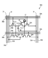
- FIG. 1 is a schematic diagram showing an exemplary configuration of an imaging device 100 according to the first embodiment.
- the imaging device 100 has a plurality of pixels 10 and peripheral circuits formed on a semiconductor substrate 60 .
- Each pixel 10 includes a photoelectric conversion unit 12.
- the photoelectric conversion unit 12 receives incident light and generates positive and negative charges. Positive and negative charges are typically hole-electron pairs.
- the photoelectric conversion part 12 is a photoelectric conversion structure including a photoelectric conversion layer arranged above the semiconductor substrate 60 .
- the photoelectric conversion unit 12 can be read as a photoelectric conversion structure.
- the photoelectric conversion unit 12 may be a photodiode formed on the semiconductor substrate 60 .
- the photoelectric conversion units 12 of each pixel 10 are shown spatially separated from each other. However, this is only for convenience of explanation.
- the photoelectric conversion units 12 of a plurality of pixels 10 may be continuously arranged on the semiconductor substrate 60 without spacing.
- pixels 10 are arranged in a plurality of rows and columns of m rows and n columns.
- m and n independently represent an integer of 1 or more.
- the pixels 10 form an imaging region R1 by being arranged two-dimensionally on the semiconductor substrate 60, for example.
- the number and arrangement of pixels 10 are not limited to the illustrated example.
- the center of each pixel 10 is positioned on a lattice point of a square lattice.
- a plurality of pixels 10 may be arranged such that the center of each pixel 10 is positioned on a lattice point such as a triangular lattice or a hexagonal lattice.
- the imaging device 100 may be used as a line sensor.
- the number of pixels 10 included in the imaging device 100 may be one.
- the peripheral circuits include a vertical scanning circuit 42 and a horizontal signal readout circuit 44.
- the peripheral circuitry may additionally include control circuitry 46 and voltage supply circuitry 48 .
- the peripheral circuit may further include a signal processing circuit, an output circuit, and the like.
- each circuit included in the peripheral circuit is provided on the semiconductor substrate 60 .
- part of the peripheral circuit may be arranged on another substrate different from the semiconductor substrate 60 on which the pixels 10 are formed.
- the vertical scanning circuit 42 is also called a row scanning circuit.
- the vertical scanning circuit 42 is connected to the address signal lines 34 provided for each row of the plurality of pixels 10 .
- the signal lines provided for each row of the plurality of pixels 10 are not limited to the address signal lines 34 .
- a plurality of types of signal lines can be connected to the vertical scanning circuit 42 for each row of the plurality of pixels 10 .
- the horizontal signal readout circuit 44 is also called a column scanning circuit.
- the horizontal signal readout circuit 44 is connected to the vertical signal lines 35 provided for each column of the plurality of pixels 10 .
- the control circuit 46 receives instruction data, clocks, etc. given from the outside of the imaging device 100 and controls the imaging device 100 as a whole. Typically, control circuit 46 has a timing generator. The control circuit 46 supplies drive signals to the vertical scanning circuit 42, the horizontal signal readout circuit 44, the voltage supply circuit 48, and the like. Arrows extending from the control circuit 46 in FIG. 1 schematically represent the flow of output signals from the control circuit 46 .
- Control circuitry 46 may be implemented by, for example, a microcontroller or one or more processors. A microcontroller may include one or more processors. The functions of the control circuit 46 may be realized by a combination of a general-purpose processing circuit and software, or by hardware specialized for such processing.
- a voltage supply circuit 48 supplies a predetermined voltage to each pixel 10 via the voltage line 38 .
- Voltage supply circuit 48 is not limited to a specific power supply circuit.
- the voltage supply circuit 48 may be a circuit that converts a voltage supplied from a power source such as a battery into a predetermined voltage, or may be a circuit that generates a predetermined voltage.
- the voltage supply circuit 48 may be part of the vertical scanning circuit 42 described above. As schematically shown in FIG. 1, these circuits forming a peripheral circuit are arranged in a peripheral region R2 outside the imaging region R1.
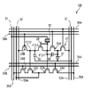
- FIG. 2 is a schematic diagram showing an exemplary circuit configuration of the pixel 10 of the imaging device 100 according to the first embodiment.
- one pixel 10A is shown as a representative to avoid complicating the drawing.
- Pixel 10A is an example of pixel 10 shown in FIG.
- the pixel 10A has a photoelectric conversion section 12 .
- the pixel 10A also includes a signal detection circuit electrically connected to the photoelectric conversion unit 12 .
- the photoelectric conversion section 12 includes a photoelectric conversion layer arranged above the semiconductor substrate 60 . That is, here, a stacked imaging device is exemplified as the imaging device 100 .
- the photoelectric conversion section 12 is supported by the semiconductor substrate 60 .
- the photoelectric converter 12 is connected to the accumulation control line 31 .
- a predetermined potential V ITO is applied to the accumulation control line 31 during operation of the imaging apparatus 100 .
- the potential V ITO applied to the accumulation control line 31 during operation of the imaging device 100 is, for example, , is a positive potential of about 10V.
- holes are used as signal charges will be exemplified below.
- the pixel 10A includes a first amplification transistor 22A, a first address transistor 24A, a first reset transistor 26A, a first transistor 29 which is a protection transistor, a second amplification transistor 22B, a second address transistor 24B, a second reset transistor 26B, and a capacitor. Includes element 30 .
- Transistors 22A, 24A, 26A, 29, 22B, 24B, and 26B are provided on semiconductor substrate 60 .
- the semiconductor substrate 60 is a silicon substrate.
- the transistors 22A, 24A, 26A, 29, 22B, 24B and 26B are field effect transistors (FET).
- FET field effect transistors
- the transistors 22A, 24A, 26A, 29, 22B, 24B and 26B are MOSFETs (Metal Oxide Semiconductor FETs).
- the first amplification transistor 22A, the first address transistor 24A, the first reset transistor 26A, the first transistor 29, the second amplification transistor 22B and the second address transistor 24B are N-type transistors.
- transistors 22A, 24A, 26A, 29, 22B and 24B are N-type MOSFETs or NMOS.
- the second reset transistor 26B is a P-type transistor.
- the second reset transistor 26B is a P-type MOSFET, that is, a PMOS.
- a gate electrode 22Ae of the first amplification transistor 22A is electrically connected to the photoelectric conversion section 12 .
- the charge accumulation node is a node electrically connected to the gate electrode 22Ae of the first amplification transistor 22A and the photoelectric conversion section 12 .
- the charge storage node partially includes an impurity region formed in semiconductor substrate 60 .
- the charge storage node has a function of temporarily holding charges generated by the photoelectric conversion unit 12 .
- a first charge storage portion FD1 as an example of a first impurity region, a second charge storage portion FD2 and a third charge storage portion FD3 as examples of a second impurity region are provided.
- the charge storage units FD1, FD2 and FD3 are included in the charge storage node.
- the charge storage units FD1, FD2, and FD3 have a function of temporarily retaining charges.
- the first charge storage unit FD1 is one of the source and drain of the first transistor 29, which is a protection transistor.
- the first charge storage unit FD1 is also one of the source and drain of the first reset transistor 26A.
- the third charge storage unit FD3 is the other of the source and drain of the first transistor 29 .
- the second charge storage unit FD2 is one of the source and drain of the second reset transistor 26B.
- the photoelectric conversion unit 12 When the photoelectric conversion unit 12 performs photoelectric conversion, charges generated by the photoelectric conversion flow to the first charge storage unit FD1, and charges are accumulated in the first charge storage unit FD1.
- the first charge storage unit FD1 is electrically connected to the gate electrode 29e of the first transistor 29, which is a protection transistor.
- the first transistor 29 When the potential of the first charge storage unit FD1 reaches the threshold potential VOF as the charge stored in the first charge storage unit FD1 increases, the first transistor 29 is turned on (turned on). As a result, the charge in the first charge storage unit FD1 flows to the second charge storage unit FD2, the third charge storage unit FD3, and the capacitive element 30.
- FIG. Note that the threshold potential V OF is a potential that depends on the threshold voltage of the first transistor 29 .
- threshold voltage refers to the gate-to-source voltage of a transistor when drain current begins to flow through the transistor.
- the capacitive element 30 is a metal-insulator-metal (MIM) capacitor.
- M metal-insulator-metal
- the “I” in MIM is an insulator, such as an oxide.
- MIM is a concept that includes MOM (Metal Oxide Metal).
- the MIM capacitor can realize a capacitive element 30 with a high capacity density. In particular, if an insulator with a high dielectric constant is used as the insulator, it is easy to realize the capacitive element 30 with a high capacitance density.
- One end of the capacitive element 30 is electrically connected to the second charge storage section FD2 and the third charge storage section FD3.
- the other end of the capacitive element 30 is electrically connected to the capacitive terminal line 37 .
- a potential V ss is applied to the other end of the capacitive element 30 via the capacitive terminal line 37 .
- the potential V ss is a fixed potential.
- One of the source and drain of the first amplification transistor 22A and one of the source and drain of the second amplification transistor 22B are connected to the power supply wiring 32 .
- a power supply potential V DD of about 3.3 V, for example, is supplied from the power supply wiring 32 to one of the drains.
- the other of the source and drain of the first amplification transistor 22A is connected to the first output line 35A via the first address transistor 24A.
- the other of the source and drain of the second amplification transistor 22B is connected to the second output line 35B via the second address transistor 24B.
- the vertical signal line 35 shown in FIG. 1 collectively describes the first output line 35A and the second output line 35B.
- a power supply potential V DD is supplied to one of the source and the drain of the first amplification transistor 22A.
- the first amplification transistor 22A outputs an electric signal corresponding to the potential of the first charge storage section FD1 to the first output line 35A via the first address transistor 24A.
- This electrical signal is specifically a voltage signal.
- a power supply potential V DD is supplied to one of the source and the drain of the second amplification transistor 22B.
- the second amplification transistor 22B outputs an electric signal corresponding to the potential of the second charge storage section FD2 to the second output line 35B via the second address transistor 24B.
- This electrical signal is specifically a voltage signal.
- a first address transistor 24A is connected between the first amplification transistor 22A and the first output line 35A.
- a first address line 34A is connected to the gate electrode 24Ae of the first address transistor 24A.
- a second address transistor 24B is connected between the second amplification transistor 22B and the second output line 35B.
- a second address line 34B is connected to the gate electrode 24Be of the second address transistor 24B.
- the address signal lines 34 shown in FIG. 1 collectively describe the first address lines 34A and the second address lines 34B.
- the vertical scanning circuit 42 applies to the first address line 34A a row selection signal that controls turning on and off of the first address transistor 24A. Thereby, the output of the first amplification transistor 22A of the selected pixel 10A can be read out to the first output line 35A.
- the vertical scanning circuit 42 applies a row selection signal to the second address line 34B to control ON and OFF of the second address transistor 24B. Thereby, the output of the second amplification transistor 22B of the selected pixel 10A can be read out to the second output line 35B.
- the arrangement of the first address transistor 24A and the arrangement of the second address transistor 24B are not limited to the example shown in FIG.
- the first address transistor 24A may be arranged between one of the source and drain of the first amplification transistor 22A and the power supply wiring 32 .
- the second address transistor 24B may be arranged between one of the source and drain of the second amplification transistor 22B and the power supply wiring 32 .
- FIG. 3 is a schematic diagram showing an exemplary circuit configuration after the pixel 10A.
- the first output line 35A is connected to the first load circuit 45A and the first column signal processing circuit 47A.
- the first load circuit 45A forms a source follower circuit together with the first amplification transistor 22A.
- the first column signal processing circuit 47A performs noise suppression signal processing, analog-digital conversion, and the like.
- the second output line 35B is connected to the second load circuit 45B and the second column signal processing circuit 47B.
- the second load circuit 45B forms a source follower circuit together with the second amplification transistor 22B.
- the second column signal processing circuit 47B performs noise suppression signal processing, analog-digital conversion, and the like.
- the column signal processing circuits 47A and 47B are also called row signal storage circuits.
- the noise suppression signal processing of the column signal processing circuits 47A and 47B is, for example, correlated double sampling.
- the column signal processing circuits 47A and 47B are connected to the horizontal signal readout circuit 44.
- the horizontal signal readout circuit 44 is connected to a first horizontal signal line and a second horizontal signal line (not shown).
- the horizontal signal readout circuit 44 reads signals from the first column signal processing circuit 47A to the first horizontal signal line, and reads signals from the second column signal processing circuit 47B to the second horizontal signal line. In this way, the signal that has passed through the first column signal processing circuit 47A and the signal that has passed through the second column signal processing circuit 47B can be read out in parallel. This is advantageous from the point of view of reading out these signals in a short time.
- a first load circuit 45A is provided for each column of a plurality of pixels 10A. The same applies to the second load circuit 45B, the first column signal processing circuit 47A and the second column signal processing circuit 47B. Load circuits 45A and 45B and column signal processing circuits 47A and 47B may be part of the peripheral circuits described above.
- a vertical scanning circuit 42 is connected to the gate electrode 26Ae of the first reset transistor 26A via the first reset line 36A.
- the first reset line 36A is provided for each row of the plurality of pixels 10A, like the first address line 34A and the second address line 34B.
- the vertical scanning circuit 42 can select the pixels 10A to be reset on a row-by-row basis by applying a row selection signal to the first address line 34A. By applying a reset signal to the gate electrode 26Ae of the selected row, the first reset transistor 26A of the selected row can be turned on. By turning on the first reset transistor 26A, the potential of the first charge storage section FD1 is reset.
- a vertical scanning circuit 42 is connected to the gate electrode 26Be of the second reset transistor 26B via a second reset line 36B.
- the second reset line 36B is provided for each row of the plurality of pixels 10A, like the first reset line 36A.
- the vertical scanning circuit 42 can select the pixels 10A to be reset on a row-by-row basis by applying a row selection signal to the second address line 34B.
- the second reset transistor 26B of the selected row can be turned on.
- the potential of the second charge storage section FD2 is reset.
- the potentials of the third charge storage section FD3 and the capacitive element 30 are reset along with the potential of the second charge storage section FD2.
- one of the drain and source of the first reset transistor 26A is the first charge storage unit FD1.
- the other of the drain and source of the first reset transistor 26A is electrically connected to the first feedback line 53A.
- the potential of the first feedback line 53A is supplied to the first charge storage section FD1 as the reset potential VRES for resetting the charge of the first charge storage section FD1.
- one of the drain and source of the second reset transistor 26B is the second charge storage unit FD2.
- the other of the drain and source of the second reset transistor 26B is electrically connected to the second feedback line 53B.
- the potential of the second feedback line 53B is supplied to the second charge storage section FD2 as the reset potential for resetting the charge of the second charge storage section FD2.
- the imaging device 100 has a first feedback circuit 16A including a first inverting amplifier 50A as part of the feedback path.
- the first feedback line 53A is connected to the output terminal of the first inverting amplifier 50A.
- the imaging device 100 has a second feedback circuit 16B including a second inverting amplifier 50B as part of the feedback path.
- the second feedback line 53B is connected to the output terminal of the second inverting amplifier 50B.
- the inverting input terminal of the first inverting amplifier 50A is connected to the first output line 35A.
- a first reference potential Vref1 is supplied to the non-inverting input terminal of the first inverting amplifier 50A when the imaging device 100 is in operation.
- the first reference potential Vref1 is, for example, a positive potential of 1V or around 1V.
- the formation of the feedback path resets the potential of the first charge storage unit FD1 to a potential that makes the potential of the first output line 35A equal to Vref1.
- Vref1 any potential magnitude within the range between the power supply potential VDD and the ground can be used.
- the inverting input terminal of the second inverting amplifier 50B is connected to the second output line 35B.
- a second reference potential Vref2 is supplied to the non-inverting input terminal of the second inverting amplifier 50B when the imaging device 100 is in operation.
- the second reference potential Vref2 is a positive potential higher than the first reference potential Vref2.
- the formation of the feedback path resets the potential of the second charge storage unit FD2 to a potential that makes the potential of the second output line 35B equal to Vref2.
- Vref2 a potential of any magnitude within the range of the power supply potential VDD and ground can be used.
- the first inverting amplifier 50A is provided for each column of the plurality of pixels 10A. The same applies to the second inverting amplifier 50B, the first feedback line 53A, the second feedback line 53B, the first feedback circuit 16A, and the second feedback circuit 16B. Inverting amplifiers 50A and 50B may be part of the peripheral circuitry described above.
- a column feedback circuit is configured in this embodiment. Feedback can suppress reset noise.
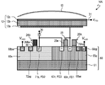
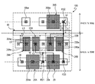
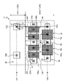
- FIG. 4 is a schematic plan view showing an example layout of each element in the pixel 10A according to the first embodiment.
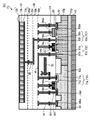
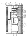
- FIG. 5 is a cross-sectional view schematically showing the arrangement of elements in the pixel 10A shown in FIG. If the pixel 10A is cut along the broken line VV in FIG. 4 and expanded, the cross section shown in FIG. 5 is obtained.
- the pixel 10A generally includes a semiconductor substrate 60, a photoelectric conversion section 12, and a conductive structure 89.
- the photoelectric conversion section 12 is arranged above the semiconductor substrate 60 .
- the photoelectric conversion section 12 is supported by the interlayer insulating layer 90 .
- An interlayer insulating layer 90 covers the semiconductor substrate 60 .
- Conductive structure 89 is disposed within interlayer insulating layer 90 .
- the interlayer insulating layer 90 includes multiple insulating layers.
- the multiple wiring layers include a first wiring layer and a second wiring layer.
- the first wiring layer includes address lines 34A and 34B, reset lines 36A and 36B, and the like.
- the second wiring layer includes output lines 35A and 35B, power supply wiring 32, feedback lines 53A and 53B, and the like.
- the number of insulating layers and the number of wiring layers in the interlayer insulating layer 90 are not limited to this example and can be set arbitrarily.
- the photoelectric conversion unit 12 converts incident light into electric charge.
- the photoelectric conversion section 12 includes a pixel electrode 12a, a counter electrode 12c, and a photoelectric conversion layer 12b.
- the pixel electrode 12 a is provided on the interlayer insulating layer 90 .
- the counter electrode 12c is arranged on the light incident side of the pixel electrode 12a.
- the photoelectric conversion layer 12b is arranged between these electrodes 12a and 12c.
- the photoelectric conversion layer 12b receives incident light through the counter electrode 12c and performs photoelectric conversion. Photoelectric conversion produces positive and negative charges.
- the photoelectric conversion layer 12b is typically provided continuously over a plurality of pixels 10A.
- the photoelectric conversion layer 12b is made of organic material or inorganic material. Amorphous silicon is exemplified as an inorganic material.
- the photoelectric conversion layer 12b may include a layer of organic material and a layer of inorganic material.
- the counter electrode 12c is provided over a plurality of pixels 10A, similar to the photoelectric conversion layer 12b.
- the counter electrode 12c is connected to the storage control line 31 described above.
- the potential of the storage control line 31 is controlled to make the potential of the counter electrode 12c higher than the potential of the pixel electrode 12a. This allows the pixel electrodes 12a to selectively collect the positive charges out of the positive and negative charges generated by photoelectric conversion.
- the counter electrode 12c is a translucent electrode.
- the counter electrode 12c is made of a transparent conductive material.
- ITO Indium Thin Oxide
- the term “translucent” in this specification means that at least a part of light having a wavelength that can be absorbed by the photoelectric conversion layer 12b is transmitted, and it is essential to transmit light over the entire wavelength range of visible light. is not.
- the pixel electrode 12a is spatially separated from the pixel electrode 12a of another adjacent pixel 10A. Thereby, the pixel electrode 12a is electrically isolated from the pixel electrodes 12a of the other pixels 10A.
- the pixel electrode 12a is made of metal or metal nitride. Aluminum, copper, etc. are illustrated as a metal.
- the pixel electrode 12a may be made of polysilicon or the like that is doped with an impurity to provide conductivity.
- the conductive structure 89 includes a plurality of wirings, plugs cp, contact plugs cpn and contact plugs cpp. One end of the conductive structure 89 is connected to the pixel electrode 12a. The other end of conductive structure 89 is connected to a circuit element formed on semiconductor substrate 60 . Thereby, the pixel electrode 12a of the photoelectric conversion section 12 and the circuit on the semiconductor substrate 60 are electrically connected to each other.
- multiple wirings and plugs cp are made of metal or metal compound. Copper, tungsten, etc. are illustrated as a metal. Examples of metal compounds include metal nitrides and metal oxides.
- Contact plugs cpn and cpp are made of polysilicon.
- the contact plug cpn is an N-type contact plug.
- the N-type contact plug cpn is doped with phosphorus, for example.
- the contact plug cpp is a P-type contact plug.
- the P-type contact plug cpp is doped with boron, for example.
- the contact plugs cpn and cpp have bar-shaped portions.
- the semiconductor substrate 60 includes a support substrate 61 and one or more semiconductor layers formed on the support substrate 61 .
- a silicon substrate specifically a P-type silicon substrate is exemplified.
- the semiconductor substrate 60 includes a P-type semiconductor region 61p, a first well region 65p that is a P-well region, a second well region 65n that is an N-well region, an impurity region 66n, an impurity region 67n, an impurity region 68an, An impurity region 68bn, an impurity region 71p, an impurity region 72ap and an element isolation region 69 are included.
- the P-type semiconductor region 61 p is arranged on the support substrate 61 .
- the P-type semiconductor region 61p contains P-type impurities at a lower concentration than the support substrate 61 does.
- the first well region 65p which is a P-well region, is a P-type impurity region.
- the first well region 65p is arranged on the P-type semiconductor region 61p.
- the first well region 65p contains P-type impurities. Specifically, the first well region 65p contains P-type impurities at a concentration lower than that of the support substrate 61 and higher than that of the P-type semiconductor region 61p.
- the second well region 65n which is an N-well region, is an N-type impurity region.
- the second well region 65n is arranged on the P-type semiconductor region 61p.
- the second well region 65n contains N-type impurities.
- the "NMOS Tr. region” is the region where the first well region 65p extends in plan view.
- the "PMOS Tr. region” is a region where the second well region 65n extends in plan view.
- an insulating layer 80 is provided on the semiconductor substrate 60 .
- the insulating layer 80 serves as the gate insulating film of the first amplification transistor 22A, the first address transistor 24A, the first reset transistor 26A, the first transistor 29, the second amplification transistor 22B, the second address transistor 24B, and the second reset transistor 26B.
- the first reset transistor 26A includes an impurity region 66n as one of its source and drain.
- the first reset transistor 26A includes an impurity region 68an as the other of the source and drain.
- the first reset transistor 26A includes an insulating layer 80 and a gate electrode 26Ae.
- the gate electrode 26Ae is provided on the insulating layer 80 .
- the first transistor 29, which is a protection transistor, includes an impurity region 66n as one of its source and drain.
- the first transistor 29 includes an impurity region 67n as the other of the source and drain.
- the first transistor 29 includes an insulating layer 80 and a gate electrode 29e. Gate electrode 29 e is provided on insulating layer 80 .
- the impurity region 66n is also the first charge storage unit FD1.
- the impurity region 67n is also the third charge storage unit FD3.
- the second reset transistor 26B includes an impurity region 71p as one of its source and drain.
- the second reset transistor 26B includes an impurity region 72ap as the other of the source and drain.
- the second reset transistor 26B includes an insulating layer 80 and a gate electrode 26Be.
- the gate electrode 26Be is provided on the insulating layer 80 .
- the impurity region 71p is also the second charge storage unit FD2.
- the impurity regions 66n, 67n, 68an and 68bn are N-type impurity regions.
- the impurity regions 71p and 72ap are P-type impurity regions.
- the impurity region 66n is arranged within the first well region 65p.
- the impurity region 66n includes a first region 66a and a second region 66b.
- the second region 66b is provided within the first region 66a.
- the second region 66b has a higher impurity concentration than the first region 66a.
- the impurity region 67n is arranged within the first well region 65p.
- the impurity region 67n includes a first region 67a and a second region 67b.
- the second region 67b is provided within the first region 67a.
- the second region 67b has a higher impurity concentration than the first region 67a.
- the impurity region 71p is arranged within the second well region 65n.
- the impurity region 71p includes a first region 71a and a second region 71b.
- the second region 71b is provided within the first region 71a.
- the second region 71b has a higher impurity concentration than the first region 71a.
- the impurity region 68an is arranged within the first well region 65p.
- Impurity region 68bn is arranged in second well region 65n.
- Impurity region 72ap is arranged in second well region 65n.
- the impurity region 68bn constitutes a well contact region of the second well region 65n. By applying a potential to impurity region 68bn, the potential of second well region 65n can be adjusted. Although not shown in FIG. 5, there is also an impurity region 68cp forming a well contact region of the first well region 65p. Impurity region 68cp is a P-type impurity region. By applying a potential to the impurity region 68cp, the potential of the first well region 65p can be adjusted.
- the impurity region 68an has a first region and a second region having a higher impurity concentration than the first region. This point also applies to the impurity regions 72ap, 68bn and 68cp.
- the first amplification transistor 22A, the first address transistor 24A, the first reset transistor 26A, the first transistor 29, the second amplification transistor 22B and the second address transistor 24B are NMOS.
- the second reset transistor 26B is a PMOS.
- the element isolation region 69 divides the second reset transistor 26B, which is a PMOS, into the first amplification transistor 22A, the first address transistor 24A, the first reset transistor 26A, the first transistor 29, the second amplification transistor 22B, and the second amplification transistor 22A, which are NMOS. It is electrically isolated from the address transistor 24B.
- the element isolation region 69 has a shallow trench isolation (STI) structure.
- An STI structure may be formed in the semiconductor substrate 60 by an STI process.
- the element isolation region 69 may be an implantation isolation region.
- the element isolation region 69 surrounds the first charge storage portion FD1 in plan view.
- the element isolation region 69 surrounds the second charge storage portion FD2 in plan view.
- the element isolation region 69 surrounds the third charge storage portion FD3 in plan view.
- the gate electrode 24Be of the 2-address transistor 24B is a gate electrode doped with an N-type impurity.
- the gate electrode 26Be of the second reset transistor 26B is a gate electrode doped with P-type impurities.
- the interlayer insulating layer 90 includes a plurality of insulating layers 90a, 90b, 90c and an insulating layer 90d.
- the number of insulating layers included in interlayer insulating layer 90 is not particularly limited.
- the plurality of plugs cp, the plurality of contact plugs cpn, and the plurality of contact plugs cpp are arranged in the insulating layer 90a.
- the plug cp, contact plug cpn and impurity region 68an are electrically connected in this order.
- the plug cp, contact plug cpp and impurity region 72ap are electrically connected in this order.
- the plug cp, contact plug cpn and impurity region 68bn are electrically connected in this order.
- the connection destination of these contact plugs cpn or cpp is the second impurity region.
- the plug cp, contact plug cpn, and gate electrode 26Ae are electrically connected in this order.
- the plug cp, contact plug cpn and gate electrode 29e are electrically connected in this order.
- the plug cp, contact plug cpp and gate electrode 26Be are electrically connected in this order.
- the pixel electrode 12a, plug cp, contact plug cpn, and impurity region 66n are electrically connected in this order. Therefore, the charge collected by the pixel electrode 12a is transmitted to the impurity region 66n through the plug cp and the contact plug cpn in this order.
- the connection destination of this contact plug cpn is the second region 66b of the impurity region 66n.
- the impurity region 67n, contact plug cpn, plug cp, wiring wr, plug cp, contact plug cpp, and impurity region 71p are electrically connected in this order.
- the second region 67b of the impurity region 67n, the contact plug cpn, the plug cp, the wiring wr, the plug cp, the contact plug cpp, and the second region 71b of the impurity region 71p are electrically connected in this order.
- the formation of a PN junction is avoided by interposing a metal or metal compound plug cp between contact plugs cpn and cpp of opposite conductivity types. It is also possible to directly connect the contact plugs cpn and cpp while avoiding the formation of the PN junction, for example, by siliciding the junctions of the contact plugs cpn and cpp.
- the insulating layer 80 is actually located under the gate electrodes of the transistors 22A, 24A, 26A, 29, 22B, 24B and 26B in the region on the semiconductor substrate 60. It is also provided in other areas. Specifically, the insulating layer 80 extends in the form of a film over the semiconductor substrate 60 in a region below the gate electrode and a region other than the region below the gate electrode.
- An insulating layer 85 is provided on the gate electrodes of the transistors 22A, 24A, 26A, 29, 22B, 24B and 26B. Specifically, the insulating layer 85 extends like a film over a portion of the insulating layer 80 that extends in a region other than under the gate electrode and over the gate electrode.
- the contact plug cpn is connected to the impurity region 68an through a contact hole.
- Contact plug cpp is connected to impurity region 72ap through a contact hole.
- Contact plug cpn is connected to impurity region 68bn through a contact hole.
- the contact plug cpn is connected to the gate electrode 26Ae through a contact hole.
- Contact plug cpn is connected to gate electrode 29e through a contact hole.
- the contact plug cpp is connected to the gate electrode 26Be through a contact hole.
- Contact plug cpn is connected to impurity region 66n through a contact hole.
- Contact plug cpn is connected to impurity region 67n through a contact hole.
- Contact plug cpp is connected to impurity region 71p through a contact hole.
- a contact plug cpn not drawn in FIG. 5 also exists.
- the contact plug cpn is connected to the gate electrode 22Ae of the first amplification transistor 22A through a contact hole.
- the contact plug cpn is connected to the gate electrode 22Be of the second amplification transistor 22B through a contact hole.
- the contact plug cpn is connected to the gate electrode 24Ae of the first address transistor 24A through a contact hole.
- the contact plug cpn is connected to the gate electrode 24Be of the second address transistor 24B through a contact hole.
- Each contact hole through which the contact plugs cpn or cpp connected to the impurity regions 68an, 72ap, 68bn, 66n, 67n and 71p pass is provided to penetrate the insulating layers 80 and 85 .
- Each contact hole through which the contact plug cpn or cpp connected to the gate electrodes 26Ae, 29e, 26Be, 22Ae, 22Be, 24Ae and 24Be passes is provided to penetrate the insulating layer 85 .
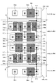
- FIG. 4 shows the first contact hole h1 through which the contact plug cpn connected to the impurity region 66n, that is, the first charge storage portion FD1 passes.
- a second contact hole h2 is shown through which the contact plug cpp connected to the impurity region 71p, that is, the second charge storage portion FD2 passes.
- a third contact hole h3 through which a contact plug cpn connected to the gate electrode 22Ae passes is shown.
- a fourth contact hole h4 through which a contact plug cpn connected to impurity region 68an passes is shown.
- a fifth contact hole h5 through which a contact plug cpn connected to the gate electrode 26Ae passes is shown.
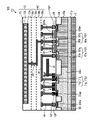
- FIG. 6 is a cross-sectional view schematically showing the structure of the first reset transistor 26A and its periphery according to the first embodiment.
- a first contact hole h1 through which a contact plug cpn connected to the impurity region 66n passes is provided to penetrate the insulating layers 80 and 85.
- a fourth contact hole h4 through which the contact plug cpn connected to the impurity region 68an passes is provided to penetrate the insulating layers 80 and 85 .
- Contact holes through which the contact plugs cpn or cpp connected to the impurity regions 72ap, 68bn, 67n and 71p pass are similarly provided to penetrate the insulating layers 80 and 85 .
- the fifth contact hole h5 through which the contact plug cpn connected to the gate electrode 26Ae passes is provided to penetrate the insulating layer 85.
- Contact holes through which contact plugs cpn or cpp connected to the gate electrodes 29e, 26Be, 22Ae, 22Be, 24Ae, and 24Be pass are similarly provided to penetrate the insulating layer 85.
- FIG. 7 is a cross-sectional view schematically showing the pixel 10A according to the first embodiment.
- the microlens 13 arranged on the photoelectric conversion section 12 is shown.
- illustration of the P-type semiconductor region 61p, the element isolation region 69, and the like is omitted.
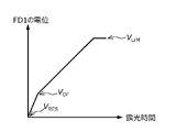
- FIG. 8 is a graph schematically showing the relationship between the exposure time of the imaging device 100 and the potential of the first charge storage section FD1 according to the first embodiment.
- impurity region 68cp constitutes a well contact region of first well region 65p.
- a first bias potential V sub is applied to the impurity region 68cp.
- the first bias potential V sub is, for example, 0V.
- impurity region 68bn constitutes a well contact region of second well region 65n.
- a second bias potential V NW is applied to the impurity region 68bn.
- the second bias potential V NW is, for example, 3.3V.
- the first charge accumulation unit FD1 during exposure of the imaging device 100 will be described with reference to FIG.
- the potential of the first charge storage section FD1 is reset to the reset potential VRES by a reset operation using the first reset transistor 26A. After that, as the exposure progresses, the charge accumulation in the first charge accumulation unit FD1 progresses, and the potential of the first charge accumulation unit FD1 rises.
- the first charge storage section FD1 When the potential of the first charge storage unit FD1 reaches the threshold potential V OF , the source-drain voltage of the first transistor 29, which is a protection transistor, becomes the threshold voltage, and the first transistor 29 is turned on. As a result, the first charge storage section FD1 is electrically connected to the second charge storage section FD2, the third charge storage section FD3, and the capacitive element 30, and accumulates charges in cooperation with them. In other words, the capacitance value of the charge storage node is larger after turn-on than before turn-on. Therefore, after turn-on, the slope of change in the potential of the first charge storage unit FD1 with respect to the exposure time is smaller than before turn-on.
- the potential of the first charge storage unit FD1 rises.
- the potential of the second charge storage section FD2 electrically connected to the first charge storage section FD1.
- V CLIP clipping potential
- a forward bias voltage is applied to the PN junction between the second charge storage section FD2 and the second well region 65n, which is the N well region.
- the charge is discharged from the second charge storage portion FD2 to the second well region 65n.
- the clipping potential V CLIP is a potential dependent on the second bias potential V NW .
- the relationship between the second bias potential V NW and the clipping potential V CLIP will be described.
- a PN junction is formed between the second well region 65n and the second charge storage section FD2.
- the clipping potential V CLIP deviates from the second bias potential V NW due to the built-in potential V bi of this PN junction.
- the built-in potential Vbi takes a value according to the impurity concentration of the second well region 65n and the impurity concentration of the second charge storage section FD2.
- the clipping potential V CLIP is the sum of the second bias potential V NW and the built-in potential V bi .
- the PN junction current that is, the current in the forward bias direction begins to flow when the potential of the second charge storage section FD2 becomes the potential near the second bias potential V NW due to the generation of charges, and then the current gradually increases. grow to Typically, the second bias potential V NW and the clipping potential V CLIP are approximately equal.
- the capacitance value of the charge accumulation node is small in a dark scene. Therefore, high-sensitivity imaging in a dark scene is possible.
- the capacitance value of the charge storage node is large. Therefore, highly saturated imaging is possible in a bright scene. For this reason, according to the present embodiment, the imaging apparatus 100 with a wide dynamic range can be realized.
- the reverse bias voltage applied to the PN junction between the first charge storage unit FD1 and the first well region 65p, which is the P well region, is applied to the charge storage unit FD1. smaller when is not progressing. Therefore, the leakage current of the first charge storage unit FD1 is smaller when the charge storage of the first charge storage unit FD1 is not progressing.
- This characteristic is advantageous from the viewpoint of performing high-sensitivity imaging in a dark scene. As a result, this characteristic can contribute to the realization of the imaging device 100 with a wide dynamic range.
- the potential of the first charge storage unit FD1 is prevented from changing beyond the limit potential V LIM . Together with the large capacitance value of the charge storage node in a bright scene, this makes it possible to realize the imaging device 100 that is less likely to fail even when a large amount of light is incident.
- the first transistor 29, which is a protective transistor When the first transistor 29, which is a protective transistor, is turned on, a channel through which charges pass is formed between the source and drain of the first transistor 29.
- the resistance of this channel may be referred to as channel resistance.
- the potential of the second charge storage unit FD2 can change with a delay with respect to the change of the potential of the first charge storage unit FD1.
- a difference can occur between the potential of the first charge storage unit FD1 and the potential of the second charge storage unit FD2 due to the presence of channel resistance and delay. Assuming that the channel resistance is zero, the potential of the first charge storage section FD1 and the potential of the second charge storage section FD2 can be treated as equal after a time sufficient for the RC time constant has passed.
- a difference due to channel resistance may occur between the limiting potential V LIM for the first charge storage section FD1 and the clipping potential V CLIP for the second charge storage section FD2. Considering the channel resistance to be zero, this difference can be treated as zero.
- the first transistor 29 corresponds to a protection transistor.
- the first well region 65p corresponds to the P well region.
- the second well region 65n corresponds to the N well region.
- the first impurity region corresponds to the first charge storage portion FD1.
- the second impurity region corresponds to the second charge accumulation portion FD2.
- the first conductivity type and the second conductivity type are different conductivity types. Specifically, the first conductivity type and the second conductivity type are conductivity types of opposite polarities.
- the first conductivity type is N type.
- the second conductivity type is P type.
- the first bias potential V sub and the second bias potential V NW are different potentials. It should be noted that the use of common reference numerals is not intended to limit the interpretation of this disclosure.
- imaging device 100 includes semiconductor substrate 60 .
- a semiconductor substrate 60 is provided with a first transistor 29 .
- the semiconductor substrate 60 has a first well region 65p, a second well region 65n, a first impurity region that is the first charge storage unit FD1, and a second impurity region that is the second charge storage unit FD2.
- the first well region 65p is a region of the second conductivity type.
- the second well region 65n is a first conductivity type region.
- the first impurity region is located within the first well region 65p.
- the first impurity region is one of the source and drain of the first transistor 29 .
- the first impurity region holds charges generated by photoelectric conversion.
- the first impurity region is electrically connected to the gate electrode 29 e of the first transistor 29 .
- the first impurity region is a first conductivity type impurity region.
- the second impurity region is located within the second well region 65n.
- the second impurity region is electrically connected to the other of the source and drain of the first transistor 29 .
- the second impurity region is of the second conductivity type.
- the first bias potential V sub is applied to the first well region 65p.
- a second bias potential V NW is applied to the second well region 65n.
- Application of the first bias potential V sub to the first well region 65p can stabilize the potential of the first well region 65p.
- Application of the second bias potential V NW to the second well region 65n can stabilize the potential of the second well region 65n. Further, by applying the second bias potential V NW to the second well region 65n, it is possible to adjust the potential when the change in the potential of the second impurity region due to the generation of charges by photoelectric conversion is stopped.
- the first transistor 29 is turned on when the potential of the first impurity region, which is the first charge storage section FD1, reaches the threshold potential VOF .
- the threshold potential V OF is greater than one of the first bias potential V sub and the second bias potential V NW and less than the other of the first bias potential V sub and the second bias potential V NW .
- the threshold potential V OF is greater than the first bias potential V sub and less than the second bias potential V NW .
- the threshold potential V OF may be smaller than the first bias potential V sub and larger than the second bias potential V NW .
- the potential of the second impurity region which is the second charge storage portion FD2
- the potential of the second impurity region can change as charges are generated. Then, when the potential of the second impurity region reaches a potential corresponding to the second bias potential V NW , the change in potential of the second impurity region can be stopped.
- a potential corresponding to the second bias potential V NW may be a clipping potential V CLIP .
- the first transistor 29 when the first transistor 29 is on, the first impurity region that is the first charge storage unit FD1 and the second impurity region that is the second charge storage unit FD2 are electrically connected.
- the second bias potential V NW By applying the second bias potential V NW to the second well region 65n, it is possible to adjust the potential when the change in the potential of the first impurity region due to the generation of charges by photoelectric conversion is stopped.
- the potential of the first impurity region can change as charges are generated. Then, when the potential of the first impurity region reaches a potential corresponding to the second bias potential V NW , the change in potential of the first impurity region can be stopped.
- the imaging device 100 includes an impurity region 68cp that is the first well contact region.
- the first well contact region is of the second conductivity type.
- the first well contact region is located within the first well region 65p.
- a first bias potential V sub is applied to the first well contact region.
- the first bias potential V sub can be applied to the first well region 65p through the first well contact region. By doing so, the potential of the first well region 65p can be stabilized.
- the imaging device 100 includes impurity regions 68bn that are second well contact regions.
- the second well contact region is of the first conductivity type.
- the second well contact region is located within the second well region 65n.
- a second bias potential V NW is applied to the second well contact region.
- the second bias potential V NW can be applied to the second well region 65n through the second well contact region.
- the potential of the second well region 65n can be stabilized.
- the potential when the change in potential of the second impurity region, which is the second charge storage unit FD2 associated with the generation of charges by photoelectric conversion, is stopped can be adjusted.
- the imaging device 100 includes a first contact plug that is a contact plug cpn, a first contact hole h1, a second contact plug that is a contact plug cpp, a second contact hole, a contact A third contact plug, which is a plug cpn, and a third contact hole h3 are provided.
- the semiconductor substrate 60 is provided with the first amplification transistor 22A.
- the first amplification transistor 22A outputs an electric signal corresponding to the potential of the first impurity region that is the first charge storage portion FD1.
- the source and drain of the first amplification transistor 22A are impurity regions of the first conductivity type and located in the first well region 65p.
- the first contact plug is connected to the first impurity region through the first contact hole.
- the second contact plug is connected to the second impurity region through the second contact hole.
- the third contact plug is connected to the gate electrode 22Ae of the first amplification transistor 22A through the third contact hole.
- the distance between the second well region 65n and the first contact hole h1 in plan view is defined as the distance L1.
- a distance between the first well region 65p and the second contact hole h2 in plan view is defined as a distance L2.
- a distance between the second well region 65n and the third contact hole h3 in plan view is defined as a distance L3.
- the symbol L3 and the corresponding arrow are shown at a position away from the third contact hole h3 for the sake of space. This point is the same for the code L6.
- a PN junction is formed between the first well region 65p and the second well region 65n.
- a distance L1 is a distance between this PN junction and the first contact hole h1 in plan view.
- a distance L2 is the distance between this PN junction and the second contact hole h2 in plan view.
- a distance L3 is the distance between this PN junction and the third contact hole h3 in plan view.
- the semiconductor substrate 60 is provided with an element isolation region 69 .
- the element isolation region 69 has an STI structure.
- the distance between the element isolation region 69 and the first contact hole h1 in plan view is defined as a distance L4.
- a distance between the element isolation region 69 and the second contact hole h2 in plan view is defined as a distance L5.
- a distance between the element isolation region 69 and the third contact hole h3 in plan view is defined as a distance L6.
- distance L1 is greater than distance L2.
- This configuration is rational from the viewpoint of realizing a compact imaging apparatus 100 with high image quality. Specifically, from the viewpoint of realizing a small pixel 10A, it is conceivable to reduce the sum of the distance L1 and the distance L2. On the other hand, from the viewpoint of suppressing leakage current originating from the second well region 65n in the first impurity region, which is the first charge storage portion FD1, it is conceivable to increase the distance L1. From the viewpoint of suppressing leakage current originating from the first well region 65p in the second impurity region, which is the second charge storage portion FD2, it is possible to increase the distance L2.
- the leak current in the second impurity region is reflected in the image quality when the first transistor 29 is on and the first impurity region and the second impurity region are electrically connected. At this time, since the capacitance value of the charge storage node is large, the influence of the leak current is less likely to appear on the image quality. Further, when the first transistor 29 is on, the charge is accumulated in the first impurity region to the extent that the shot noise becomes apparent, and the noise derived from the leak current of the second impurity region is hidden by the shot noise. can also be For these reasons, the leak current originating from the first well region 65p in the second impurity region has less influence on image quality than the leak current originating from the second well region 65n in the first impurity region. Considering the above, this configuration is rational from the viewpoint of realizing a compact imaging apparatus 100 with high image quality.
- distance L4 is greater than distance L5.
- This configuration is also rational from the viewpoint of realizing a compact imaging apparatus 100 with high image quality. By securing a distance from the STI structure in a plan view, it is possible to suppress leakage current resulting from a defective layer of the STI structure.
- distance L1 is greater than distance L3.
- This configuration is advantageous from the viewpoint of realizing the imaging device 100 with high image quality. Specifically, according to this configuration, it is easy to increase the distance L1. Therefore, it is easy to suppress the leakage current originating from the second well region 65n in the first impurity region, which is the first charge storage portion FD1. Specifically, it prevents impurities from the second well region 65n from diffusing into the first impurity region, and parasitic carriers generated in elements such as transistors in the second well region 65n from flowing into the first impurity region. easy to suppress.
- the distance L4 may be greater than the distance L6. This configuration is also advantageous from the viewpoint of realizing the imaging device 100 with high image quality.
- FIG. 9 is a schematic plan view showing an example layout of elements in two pixels 10A adjacent to each other.
- One of the two pixels 10A is the first pixel 10A1 and the other is the second pixel 10A2.
- the first pixel 10A1 and the second pixel 10A2 respectively include the first well region 65p, the second well region 65n, the first transistor 29, the second impurity region that is the second charge storage unit FD2, and the contact It has a first contact plug that is a plug cpn, a first contact hole h1, a third contact plug that is a contact plug cpn, a third contact hole h3, and a first amplification transistor 22A.
- the second well region 65n of the first pixel 10A1, the first well region 65p of the first pixel 10A1, the first The well region 65p and the second well region 65n of the second pixel 10A2 are arranged in this order.
- This configuration is advantageous from the viewpoint of realizing the imaging device 100 with high image quality. Specifically, according to this configuration, it is easy to secure the distance between the first impurity region, which is the first charge storage unit FD1 of the first pixel 10A1, and the second well region 65n of the second pixel 10A2. Therefore, this configuration is advantageous from the viewpoint of suppressing leakage current originating from the second well region 65n of the second pixel 10A2 in the first impurity region of the first pixel 10A1. Further, according to this configuration, it is easy to secure the distance between the first impurity region of the second pixel 10A2 and the second well region 65n of the first pixel 10A1. Therefore, this configuration is advantageous from the viewpoint of suppressing leakage current from the second well region 65n of the first pixel 10A1 in the first impurity region of the second pixel 10A2.
- the second pixel 10A2 is obtained by flipping the first pixel 10A1.
- a first pixel 10A1 in FIG. 9 corresponds to the pixel 10A in FIG.
- a second pixel 10A2 in FIG. 9 corresponds to the flipped version of the pixel 10A in FIG.
- imaging device 100 includes capacitive element 30 .
- the capacitive element 30 is electrically connected to the second impurity region, which is the second charge storage section FD2. This configuration is suitable for realizing the imaging device 100 with a wide dynamic range.
- the capacitive element 30 is an MIM capacitor. This configuration is suitable for realizing the imaging device 100 with a wide dynamic range.
- the capacitive element 30 may overlap with at least one selected from the group consisting of the first contact hole h1 and the second contact hole h2.
- the capacitive element 30 according to this configuration suppresses light incidence on at least one selected from the group consisting of the first impurity region that is the first charge storage unit FD1 and the second impurity region that is the second charge storage unit FD2. I can. Therefore, this configuration is advantageous from the viewpoint of realizing the imaging device 100 with high image quality.
- the capacitive element 30 is arranged on the insulating layer 90a.
- the capacitive element 30 can be arranged in at least one layer selected from the insulating layers 90a to 90d.
- the capacitive element 30 contains a metal or a metal compound, the light incidence suppressing effect described above is likely to appear.
- the case where the capacitive element 30 is an MIM capacitor corresponds to such a case.
- the capacitive element 30 overlaps both the first contact hole h1 and the second contact hole h2 in plan view. According to the first example, light incidence on both the first impurity region that is the first charge storage unit FD1 and the second impurity region that is the second charge storage unit FD2 can be suppressed. However, in plan view, the capacitive element 30 may overlap only one of the first contact hole h1 and the second contact hole h2. In the second example, in plan view, the capacitive element 30 overlaps the first contact hole h1, but does not overlap the second contact hole h2. As can be understood from the above description, the leak current in the first impurity region is more likely to affect image quality than the leak current in the second impurity region.
- the capacitive element 30 when there is a constraint such as a limited space for arranging the capacitive element 30, it is possible to suppress the influence of the leak current on the image quality while satisfying the constraint.
- a third example in which the capacitive element 30 does not overlap the first contact hole h1 but overlaps the second contact hole h2 in plan view can also be adopted.
- the imaging device 100 includes a first reset transistor 26A.
- the first reset transistor 26A resets the potential of the first impurity region, which is the first charge storage section FD1, to the reset potential VRES .
- the first transistor 29 is turned on when the potential of the first impurity region reaches the threshold potential VOF .
- a second bias potential V NW is applied to the second well region 65n. When the potential of the first impurity region reaches a potential corresponding to the second bias potential V NW , the potential of the first impurity region stops changing.
- the difference between the reset potential VRES and the threshold potential VOF may be smaller than the difference between the threshold potential VOF and the second bias potential VNW .
- This configuration is suitable for realizing the imaging device 100 with a wide dynamic range. Specifically, typically, the low light amount region in which high sensitivity should be emphasized is not so wide. According to this configuration, by appropriately narrowing the low-light-intensity region where the first transistor 29 is off and high sensitivity is important, the light-intensity region in which the first transistor 29 is on can be widened. Thereby, the saturation level of the imaging device 100 can be increased. Thereby, the imaging device 100 with a wide dynamic range can be realized.
- the difference between the reset potential VRES and the threshold potential VOF may be 30% or less of the difference between the threshold potential VOF and the second bias potential VNW .
- the difference between the reset potential VRES and the threshold potential VOF may be greater than 10% of the difference between the threshold potential VOF and the second bias potential VNW .
- This configuration is suitable for avoiding a situation in which the image quality of the imaging device 100 deteriorates due to noise derived from the second impurity region, which is the second charge storage section FD2.
- the reverse bias voltage applied to the PN junction between the second impurity region and the second well 65n is set to as big as Therefore, the leak current in the second impurity region is larger when the charge accumulation in the second impurity region is not progressing. Therefore, it is immediately after the first transistor 29 is turned on that the leakage current of the second impurity region is likely to be reflected in the image quality.
- the first transistor 29 when the first transistor 29 is turned on, the charge to the extent that the shot noise becomes apparent is accumulated in the first impurity region, which is the first charge accumulation unit FD1, and the shot noise causes the first impurity region to appear.
- the noise derived from the leak current of the second impurity region, which is the second charge storage section FD2 is likely to be hidden.
- the difference between the reset potential VRES and the threshold potential VOF may be greater than 12% of the difference between the threshold potential VOF and the second bias potential VNW .
- the reset potential V RES is 0V.
- the threshold potential V OF is 0.5V.
- the second bias potential V NW is 3.3V.
- the difference between the reset potential VRES and the threshold potential VOF is about 18% of the difference between the threshold potential VOF and the second bias potential VNW .
- the adjustment of the threshold potential V OF can be performed through adjustment of the threshold voltage of the first transistor 29, adjustment of the reset potential of the second impurity region which is the second charge storage section FD2, and the like.
- imaging device 100 includes photoelectric conversion unit 12 .
- the photoelectric conversion section 12 has a counter electrode 12c, a pixel electrode 12a, and a photoelectric conversion layer 12b.
- the photoelectric conversion layer 12b is arranged between the counter electrode 12c and the pixel electrode 12a.
- the photoelectric conversion layer 12b generates electric charges. Charges are led from the pixel electrode 12a to the first impurity region, which is the first charge accumulation portion FD1.
- the imaging device 100 includes a first pixel 10A.
- the first pixel 10A has a photoelectric conversion unit 12, a first transistor 29, a second impurity region that is the second charge storage unit FD2, a first well region 65p and a second well region 65n.
- the number of pixel electrodes 12a in the first pixel 10A is one.
- This configuration is suitable for realizing a fine imaging device 100 .
- a plurality of pixel electrodes exist in one pixel it is difficult to reduce the size of the image pickup device while avoiding deterioration of the characteristics of the image pickup device.
- a relatively large pixel electrode is provided in a high-sensitivity cell
- a relatively small pixel electrode is provided in a high-saturation cell
- the size ratio of the pixel electrodes produces a sensitivity ratio.
- the number of pixel electrodes 12a in the first pixel 10A is one. This configuration alleviates the difficulty of processing and miniaturizing the pixel electrode 12a, and makes it possible to miniaturize the imaging device 100 without manifesting deterioration of the characteristics of the imaging device 100 such as sensitivity at low light intensity. .
- imaging device 100 includes microlens 13 and photoelectric conversion unit 12 . Light enters the photoelectric conversion unit 12 through the microlens 13 .
- the photoelectric conversion unit 12 generates electric charges.
- the imaging device 100 includes a first pixel 10A.
- the first pixel 10A has a microlens 13, a photoelectric conversion section 12, a first transistor 29, a second impurity region which is the second charge storage section FD2, a first well region 65p and a second well region 65n.
- the number of convex surfaces of the microlens 13 in the first pixel 10A is one. This configuration is suitable for realizing a fine imaging device 100 .
- the convex surface of the microlens is made relatively large in the high-sensitivity cell
- the convex surface of the microlens is made relatively small in the high-saturation cell
- the sensitivity ratio is adjusted by the size ratio of the convex surface.
- the number of pixel electrodes 12a in the first pixel 10A is one. This configuration alleviates the difficulty of microlens processing and miniaturization, and makes it possible to reduce the size of the imaging device 100 without manifesting deterioration of the characteristics such as the oblique incidence characteristics of the imaging device 100 .
- the method for driving imaging device 100 includes a first step, a second step, and a third step.
- the first step is the step of increasing the reverse bias voltage applied to the first PN junction due to accumulation of charges generated by photoelectric conversion when the first transistor 29 is off.
- the second step is to turn on the first transistor 29 in response to charge accumulation.
- the third step is that when the first transistor 29 is on, the accumulation of charge causes the reverse bias voltage applied to the second PN junction to decrease, leading to the forward bias voltage being applied to the second PN junction, This is a step in which electric charges are discharged.
- This configuration is suitable for realizing the imaging apparatus 100 that is hard to fail even when a large amount of light is incident and has a wide dynamic range.
- the first step when the first transistor 29 is off, electric charge is generated by photoelectric conversion in the imaging device 100, and the electric charge is accumulated in a region partitioned by the first transistor 29 in the imaging device 100. This increases the reverse bias voltage applied to the first PN junction.
- the first transistor 29 is turned on when the source-drain voltage of the first transistor 29 reaches the threshold voltage by accumulating charges in the partitioned region.
- the third step when the first transistor 29 is on, charge is accumulated in the region across the first transistor 29 in the imaging device 100, thereby reducing the reverse bias voltage applied to the second PN junction. As a result, a forward bias voltage is applied to the second PN junction, thereby discharging the charge.
- the first PN junction can be the PN junction between the first impurity region, which is the first charge storage unit FD1, and the first well region 65p.
- the second PN junction may be a PN junction between the second impurity region, which is the second charge storage unit FD2, and the second well region 65n.
- FIG. 10 is a schematic plan view showing an example layout of elements in a pixel 10B according to the second embodiment.
- the element isolation region 69 extends like a strip along the PN junction between the first well region 65p and the second well region 65n.
- the element isolation region 69 has an STI structure.
- a PN junction can be formed between the element isolation region 69 and the support substrate 61 in the thickness direction of the semiconductor substrate 60 .
- the magnitude relationship of distance L1>distance L2 when the magnitude relationship of distance L4>distance L5 is also likely to be established.
- the magnitude relationship of distance L4>distance L6 is also likely to be established.
- FIG. 11 is a schematic plan view showing an example layout of elements in two pixels 10B adjacent to each other.
- One of the two pixels 10B is the first pixel 10B1 and the other is the second pixel 10B2.
- the first pixel 10B1 and the second pixel 10B2 respectively include a first well region 65p, a second well region 65n, a first transistor 29, a second impurity region that is the second charge storage unit FD2, and a contact. It has a first contact plug that is a plug cpn, a first contact hole h1, a third contact plug that is a contact plug cpn, a third contact hole h3, and a first amplification transistor 22A.
- the second well region 65n of the first pixel 10B1, the first well region 65p of the first pixel 10B1, the first well region 65p of the second pixel 10B2, and the first well region 65p of the second pixel 10B2 are sequentially arranged along the direction from the first pixel 10B1 to the second pixel 10B2.
- the well region 65p and the second well region 65n of the second pixel 10B2 are arranged in this order.
- the second pixel 10B2 is obtained by flipping the first pixel 10B1.
- a first pixel 10B1 in FIG. 11 corresponds to the pixel 10B in FIG.
- a second pixel 10B2 in FIG. 10 corresponds to the flipped pixel 10B in FIG.
- FIG. 12 is a cross-sectional view schematically showing the configuration of a pixel 10C according to the third embodiment.
- the gate electrode 29e of the first transistor 29, which is a protection transistor is a gate electrode doped with P-type impurities. According to this configuration, even if the channel dose of the first transistor 29 is suppressed, the threshold voltage of the first transistor 29 can be ensured due to the contribution of the work function of the gate electrode 29e. By suppressing the channel dose, it is possible to reduce the PN junction electric field intensity around the first charge storage portion FD1 and the third charge storage portion FD3 formed in the first well region 65p, thereby suppressing leakage current. can.
- the gate electrode 29e of the first transistor 29 is connected to the contact plug cpp. Specifically, the contact plug cpp is connected to the gate electrode 29e through a contact hole.
- the term "first transistor 29" will be used below to further describe the present embodiment.
- the first transistor 29 corresponds to a protection transistor.
- the conductivity type of the gate electrode 29 e of the first transistor 29 is opposite to the conductivity type of the source and drain of the first transistor 29 . According to this configuration, leakage current can be easily suppressed.
- FIG. 13 is a cross-sectional view schematically showing the configuration of a pixel 10D according to the fourth embodiment.
- the imaging device 100 has contact plugs cgn and cgp instead of the contact plugs cpn and cpp.
- the contact plugs cgn and cgp are common to the gate electrodes 22Ae, 24Ae, 26Ae, 29e, 22Be, 24Be and 26Be in that they have a film shape portion.
- the contact plugs cgn and cgp are common to the gate electrodes 22Ae, 24Ae, 26Ae, 29e, 22Be, 24Be and 26Be in that they are made of polysilicon.
- contact plugs cgn and cgp and the gate electrodes 22Ae, 24Ae, 26Ae, 29e, 22Be, 24Be and 26Be can be formed by a common film formation process. This is advantageous from the viewpoint of simplification of the manufacturing process.
- the contact plugs cgn and cgp in the fourth embodiment can also be called gate polysilicon pads.
- the heights of the contact plugs cgn and cgp and the heights of the gate electrodes 22Ae, 24Ae, 26Ae, 29e, 22Be, 24Be and 26Be are the same.
- a plug cp is connected to each of these elements aligned in height. This is also advantageous from the viewpoint of simplification of the manufacturing process.
- FIG. 14 is a cross-sectional view schematically showing the configuration of a pixel 10E according to the fifth embodiment.
- the imaging device 100 according to the fifth embodiment includes the gate electrode 29e doped with the P-type impurity described in the third embodiment, and the contact plugs cgn and cgp described in the fourth embodiment.
- FIG. 15 is a schematic diagram showing an exemplary circuit configuration of the pixel 10F of the imaging device according to the sixth embodiment.
- the pixel 10F comprises a feedback transistor 27.
- a column feedback circuit using feedback transistors 27 is configured.
- the pixel 10F includes a capacitive element 17 and a capacitive element 18 .
- the feedback transistor 27 is an N-type transistor. Specifically, feedback transistor 27 is an NMOS. Capacitive element 17 and capacitive element 18 are, for example, MIM capacitors.
- One end of the capacitive element 18 is electrically connected to the first charge storage section FD1.
- the other end of the capacitive element 18 is electrically connected to one of the source and drain of the feedback transistor 27 and one end of the capacitive element 17 .
- the other end of the capacitive element 17 is electrically connected to the capacitive terminal line 37 .
- the other of the source and drain of the feedback transistor 27 is electrically connected to the first feedback line 53A.
- First charge storage unit FD1 First charge storage unit FD1, first amplification transistor 22A, first address transistor 24A, first output line 35A, first inverting amplifier 50A, first feedback line 53A, feedback transistor 27, capacitive element 18, and first charge storage unit FD1 are connected in this order. With this connection, a signal derived from the potential of the first charge storage unit FD1 can be negatively fed back to the first charge storage unit FD1.
- One of the source and drain of the second reset transistor 26B is the second charge storage unit FD2.
- the other of the source and drain of the second reset transistor 26B is electrically connected to the second feedback line 53B.
- the second charge storage section FD2 The second charge storage section FD2, the second amplification transistor 22B, the second address transistor 24B, the second output line 35B, the second inverting amplifier 50B, the second feedback line 53B, the other of the source and the drain of the second reset transistor 26B and the second
- the two charge storage units FD2 are connected in this order. Due to this connection, a signal derived from the potential of the second charge storage section FD2 can be negatively fed back to the second charge storage section FD2.
- FIG. 16 is a schematic diagram showing an exemplary circuit configuration of the pixel 10G of the imaging device according to the seventh embodiment.
- an intra-pixel feedback circuit is constructed instead of the column feedback circuit using the inverting amplifiers 50A and 50B.
- One end of the capacitive element 18 is electrically connected to the first charge storage section FD1.
- the other end of the capacitive element 18 is electrically connected to one of the source and drain of the feedback transistor 27 and one end of the capacitive element 17 .
- the other end of the capacitive element 17 is electrically connected to the capacitive terminal line 37 .
- One of the source and drain of the first amplification transistor 22A is electrically connected to the power supply wiring 32 .
- the other of the source and drain of the first amplification transistor 22A and the one of the source and drain of the first address transistor 24A are electrically connected to the other of the source and drain of the feedback transistor 27 .
- the first charge storage section FD1, the first amplification transistor 22A, the feedback transistor 27, the capacitive element 18, and the first charge storage section FD1 are connected in this order. With this connection, a signal derived from the potential of the first charge storage unit FD1 can be negatively fed back to the first charge storage unit FD1.
- One of the source and drain of the second reset transistor 26B is the second charge storage unit FD2.
- One of the source and drain of the second amplification transistor 22B is electrically connected to the power supply wiring 32 .
- the other of the source and drain of the second amplification transistor 22B and one of the source and drain of the second address transistor 24B are electrically connected to the other of the source and drain of the second reset transistor 26B.
- the second charge storage section FD2 the other of the sources and drains of the second amplification transistor 22B and the second reset transistor 26B, and the second charge storage section FD2 are connected in this order. Due to this connection, a signal derived from the potential of the second charge storage section FD2 can be negatively fed back to the second charge storage section FD2.
- FIG. 17 is a schematic diagram showing an exemplary circuit configuration of the pixel 10H of the imaging device 100 according to the eighth embodiment.
- FIG. 18 is a schematic plan view showing an example layout of elements in a pixel 10H according to the eighth embodiment.
- FIG. 19 is a cross-sectional view schematically showing the arrangement of each element in the pixel 10H shown in FIG. 18. As shown in FIG. If the pixel 10H is cut along the broken line XIX-XIX in FIG. 18 and developed, the cross section shown in FIG. 19 is obtained.
- the second reset transistor 26B is an N-type transistor. Specifically, the second reset transistor 26B in the eighth embodiment is an NMOS. The second reset transistor 26B is provided in the first well region 65p.
- the first charge storage unit FD1 is one of the source and drain of the first transistor 29, which is a protection transistor.
- the first charge storage unit FD1 is also one of the source and drain of the first reset transistor 26A.
- the third charge storage unit FD3 is the other of the source and drain of the first transistor 29 .
- the third charge storage unit FD3 is also one of the source and drain of the second reset transistor 26B.
- the second charge storage unit FD2 is different from the source and the drain of the second reset transistor 26B.
- the second charge storage portion FD2 is the impurity region 71p. Note that in FIG. 19, the impurity region 73n is the other of the source and drain of the second reset transistor 26B. Impurity region 73n is an N-type impurity region.
- the second well region 65n within the pixel 10H can be made smaller. This is advantageous from the viewpoint of reducing the size of the pixel 10H. Further, according to the eighth embodiment, all transistors in the pixel 10H can be NMOS. This is advantageous from the viewpoint of simplifying the manufacturing process of the imaging device.
- FIG. 20 is a schematic diagram showing an exemplary circuit configuration of the pixel 10I of the imaging device 100 according to the ninth embodiment.
- FIG. 21 is a schematic plan view showing an example layout of each element in the pixel 10I according to the ninth embodiment.
- FIG. 22 is a cross-sectional view schematically showing the arrangement of elements in the pixel 10I shown in FIG. If the pixel 10I is cut along the dashed line XXII-XXII in FIG. 21 and developed, the cross section shown in FIG. 22 is obtained.
- the second reset transistor 26B is not provided.
- the second charge storage portion FD2 is the impurity region 71p.
- the imaging device has well reset lines 39 .
- a potential is applied to the second well region 65n via the well reset line 39.
- FIG. This application can reset the potential of the second charge storage unit FD2.
- the well reset line 39 applies a potential to the second well region 65n via the plug cp, contact plug cpn and impurity region 68bn in this order.
- the second well region 65n in the pixel 10I can be made smaller. This is advantageous from the viewpoint of reducing the size of the pixel 10I.
- the absence of the second reset transistor 26B is also advantageous from the viewpoint of reducing the size of the pixel 10I.
- all the transistors in the pixel 10I can be NMOS. This is advantageous from the viewpoint of simplifying the manufacturing process of the imaging device.
- the plug cp and the gate electrode 26Be are connected via the contact plug cpp.
- Plug cp and gate electrode 29e are connected via contact plug cpn.
- plug cp and gate electrode 26Be may be directly connected.
- Plug cp and gate electrode 29e may be directly connected.
- the plug cp and the gate electrode 29e are connected via the contact plug cpp.
- plug cp and gate electrode 29e may be directly connected.
- the connection between the plug cp and another gate electrode may be made indirectly through the contact plug cpn or cpp, or may be made directly.
- the imaging device of the present disclosure is useful, for example, for image sensors, digital cameras, and the like.
- the imaging device of the present disclosure can be used for medical cameras, robot cameras, security cameras, cameras mounted on vehicles, and the like.
Abstract
L'invention concerne un dispositif d'imagerie comprenant un substrat semi-conducteur et un premier transistor disposé dans le substrat semi-conducteur et ayant une première électrode de grille, une source et un drain. Le substrat semi-conducteur comprend : une première région de puits d'un second type de conductivité ; une seconde région de puits d'un premier type de conductivité différent du second type de conductivité ; une première région d'impureté du premier type de conductivité qui est positionnée dans la première région de puits, est l'une de la source et du drain, maintient la charge générée par conversion photoélectrique, et est électriquement connectée à la première électrode de grille ; et une seconde région d'impureté du second type de conductivité positionnée dans la seconde région de puits et connectée électriquement à l'autre de la source et du drain.
Priority Applications (2)
| Application Number | Priority Date | Filing Date | Title |
|---|---|---|---|
| JP2023506841A JPWO2022196155A1 (fr) | 2021-03-16 | 2022-02-03 | |
| US18/452,612 US20230403479A1 (en) | 2021-03-16 | 2023-08-21 | Imaging device and method for driving the same |
Applications Claiming Priority (2)
| Application Number | Priority Date | Filing Date | Title |
|---|---|---|---|
| JP2021-042047 | 2021-03-16 | ||
| JP2021042047 | 2021-03-16 |
Related Child Applications (1)
| Application Number | Title | Priority Date | Filing Date |
|---|---|---|---|
| US18/452,612 Continuation US20230403479A1 (en) | 2021-03-16 | 2023-08-21 | Imaging device and method for driving the same |
Publications (1)
| Publication Number | Publication Date |
|---|---|
| WO2022196155A1 true WO2022196155A1 (fr) | 2022-09-22 |
Family
ID=83320317
Family Applications (1)
| Application Number | Title | Priority Date | Filing Date |
|---|---|---|---|
| PCT/JP2022/004158 WO2022196155A1 (fr) | 2021-03-16 | 2022-02-03 | Dispositif d'imagerie et procédé de commande associé |
Country Status (3)
| Country | Link |
|---|---|
| US (1) | US20230403479A1 (fr) |
| JP (1) | JPWO2022196155A1 (fr) |
| WO (1) | WO2022196155A1 (fr) |
Citations (4)
| Publication number | Priority date | Publication date | Assignee | Title |
|---|---|---|---|---|
| JP2011119441A (ja) * | 2009-12-03 | 2011-06-16 | Sony Corp | 撮像素子およびカメラシステム |
| JP2016127593A (ja) * | 2014-12-26 | 2016-07-11 | パナソニックIpマネジメント株式会社 | 撮像装置 |
| JP2019091937A (ja) * | 2019-02-27 | 2019-06-13 | パナソニックIpマネジメント株式会社 | 撮像装置 |
| WO2020045121A1 (fr) * | 2018-08-31 | 2020-03-05 | ソニーセミコンダクタソリューションズ株式会社 | Dispositif d'imagerie à semi-conducteurs, procédé de pilotage associé et appareil électronique |
-
2022
- 2022-02-03 WO PCT/JP2022/004158 patent/WO2022196155A1/fr active Application Filing
- 2022-02-03 JP JP2023506841A patent/JPWO2022196155A1/ja active Pending
-
2023
- 2023-08-21 US US18/452,612 patent/US20230403479A1/en active Pending
Patent Citations (4)
| Publication number | Priority date | Publication date | Assignee | Title |
|---|---|---|---|---|
| JP2011119441A (ja) * | 2009-12-03 | 2011-06-16 | Sony Corp | 撮像素子およびカメラシステム |
| JP2016127593A (ja) * | 2014-12-26 | 2016-07-11 | パナソニックIpマネジメント株式会社 | 撮像装置 |
| WO2020045121A1 (fr) * | 2018-08-31 | 2020-03-05 | ソニーセミコンダクタソリューションズ株式会社 | Dispositif d'imagerie à semi-conducteurs, procédé de pilotage associé et appareil électronique |
| JP2019091937A (ja) * | 2019-02-27 | 2019-06-13 | パナソニックIpマネジメント株式会社 | 撮像装置 |
Also Published As
| Publication number | Publication date |
|---|---|
| JPWO2022196155A1 (fr) | 2022-09-22 |
| US20230403479A1 (en) | 2023-12-14 |
Similar Documents
| Publication | Publication Date | Title |
|---|---|---|
| US10879301B2 (en) | Solid-state imaging device | |
| US9602750B2 (en) | Image sensor pixels having built-in variable gain feedback amplifier circuitry | |
| US11631707B2 (en) | Imaging device | |
| US8139133B2 (en) | Photoelectric conversion device | |
| US8471310B2 (en) | Image sensor pixels with back-gate-modulated vertical transistor | |
| JP7262078B2 (ja) | 撮像装置 | |
| EP1850387B1 (fr) | Dispositif de capture d'images a semi-conducteurs | |
| US20070126039A1 (en) | Solid state imaging apparatus | |
| JP2012147169A (ja) | 固体撮像装置 | |
| CN109326618B (zh) | 摄像装置 | |
| WO2020137188A1 (fr) | Dispositif de capture d'image | |
| JP6689936B2 (ja) | 撮像装置の製造方法 | |
| JP6497541B2 (ja) | 撮像装置 | |
| CN110970453A (zh) | 摄像装置 | |
| WO2022196155A1 (fr) | Dispositif d'imagerie et procédé de commande associé | |
| JP6775206B2 (ja) | 撮像装置 | |
| JP2018050028A (ja) | 固体撮像装置及び電子機器 | |
| CN113016071A (zh) | 摄像装置 | |
| US20220208811A1 (en) | Imaging device | |
| US20230290793A1 (en) | Imaging device | |
| WO2023013366A1 (fr) | Dispositif d'imagerie | |
| US7977716B2 (en) | CMOS image sensor with improved fill-factor and reduced dark current | |
| JP2019134418A (ja) | 固体撮像素子、その駆動回路および撮像装置 | |
| JP2019029643A (ja) | 撮像装置 | |
| JP2008130975A (ja) | 固体撮像素子及びその製造方法 |
Legal Events
| Date | Code | Title | Description |
|---|---|---|---|
| 121 | Ep: the epo has been informed by wipo that ep was designated in this application |
Ref document number: 22770915 Country of ref document: EP Kind code of ref document: A1 |
|
| WWE | Wipo information: entry into national phase |
Ref document number: 2023506841 Country of ref document: JP |
|
| NENP | Non-entry into the national phase |
Ref country code: DE |
|
| 122 | Ep: pct application non-entry in european phase |
Ref document number: 22770915 Country of ref document: EP Kind code of ref document: A1 |