WO2021059882A1 - Dispositif d'imagerie - Google Patents
Dispositif d'imagerie Download PDFInfo
- Publication number
- WO2021059882A1 WO2021059882A1 PCT/JP2020/032973 JP2020032973W WO2021059882A1 WO 2021059882 A1 WO2021059882 A1 WO 2021059882A1 JP 2020032973 W JP2020032973 W JP 2020032973W WO 2021059882 A1 WO2021059882 A1 WO 2021059882A1
- Authority
- WO
- WIPO (PCT)
- Prior art keywords
- transistor
- region
- pixel
- charge storage
- imaging device
- Prior art date
Links
- 238000003384 imaging method Methods 0.000 title claims abstract description 49
- 238000009792 diffusion process Methods 0.000 claims abstract description 154
- 239000012535 impurity Substances 0.000 claims abstract description 105
- 238000006243 chemical reaction Methods 0.000 claims abstract description 80
- 238000003860 storage Methods 0.000 claims description 131
- 239000004065 semiconductor Substances 0.000 claims description 86
- 230000003321 amplification Effects 0.000 claims description 72
- 238000003199 nucleic acid amplification method Methods 0.000 claims description 72
- 239000000758 substrate Substances 0.000 claims description 62
- 238000000926 separation method Methods 0.000 claims description 58
- 239000010410 layer Substances 0.000 description 158
- 230000002093 peripheral effect Effects 0.000 description 29
- 229910021420 polycrystalline silicon Inorganic materials 0.000 description 18
- 229920005591 polysilicon Polymers 0.000 description 18
- 229910052751 metal Inorganic materials 0.000 description 15
- 239000002184 metal Substances 0.000 description 15
- 238000012545 processing Methods 0.000 description 14
- 238000012546 transfer Methods 0.000 description 12
- 239000000463 material Substances 0.000 description 10
- 238000000034 method Methods 0.000 description 10
- 239000010949 copper Substances 0.000 description 9
- 230000000875 corresponding effect Effects 0.000 description 9
- 230000000694 effects Effects 0.000 description 9
- 239000011229 interlayer Substances 0.000 description 9
- 238000002347 injection Methods 0.000 description 8
- 239000007924 injection Substances 0.000 description 8
- RYGMFSIKBFXOCR-UHFFFAOYSA-N Copper Chemical compound [Cu] RYGMFSIKBFXOCR-UHFFFAOYSA-N 0.000 description 7
- 229910052802 copper Inorganic materials 0.000 description 7
- WFKWXMTUELFFGS-UHFFFAOYSA-N tungsten Chemical compound [W] WFKWXMTUELFFGS-UHFFFAOYSA-N 0.000 description 6
- 229910052721 tungsten Inorganic materials 0.000 description 6
- 239000010937 tungsten Substances 0.000 description 6
- 239000000969 carrier Substances 0.000 description 5
- 229910044991 metal oxide Inorganic materials 0.000 description 5
- 150000004706 metal oxides Chemical class 0.000 description 5
- OAICVXFJPJFONN-UHFFFAOYSA-N Phosphorus Chemical compound [P] OAICVXFJPJFONN-UHFFFAOYSA-N 0.000 description 4
- 230000007547 defect Effects 0.000 description 4
- 238000010586 diagram Methods 0.000 description 4
- 150000004767 nitrides Chemical class 0.000 description 4
- 229910052698 phosphorus Inorganic materials 0.000 description 4
- 239000011574 phosphorus Substances 0.000 description 4
- ZOXJGFHDIHLPTG-UHFFFAOYSA-N Boron Chemical compound [B] ZOXJGFHDIHLPTG-UHFFFAOYSA-N 0.000 description 3
- 229910052796 boron Inorganic materials 0.000 description 3
- 239000013078 crystal Substances 0.000 description 3
- 150000002736 metal compounds Chemical class 0.000 description 3
- 230000008569 process Effects 0.000 description 3
- 230000001629 suppression Effects 0.000 description 3
- VYPSYNLAJGMNEJ-UHFFFAOYSA-N Silicium dioxide Chemical compound O=[Si]=O VYPSYNLAJGMNEJ-UHFFFAOYSA-N 0.000 description 2
- 230000008901 benefit Effects 0.000 description 2
- 230000008859 change Effects 0.000 description 2
- 238000005516 engineering process Methods 0.000 description 2
- 229910010272 inorganic material Inorganic materials 0.000 description 2
- 239000011147 inorganic material Substances 0.000 description 2
- 238000009413 insulation Methods 0.000 description 2
- 239000012212 insulator Substances 0.000 description 2
- 238000004519 manufacturing process Methods 0.000 description 2
- 239000011368 organic material Substances 0.000 description 2
- 230000003071 parasitic effect Effects 0.000 description 2
- 229910052814 silicon oxide Inorganic materials 0.000 description 2
- 229910052581 Si3N4 Inorganic materials 0.000 description 1
- XUIMIQQOPSSXEZ-UHFFFAOYSA-N Silicon Chemical compound [Si] XUIMIQQOPSSXEZ-UHFFFAOYSA-N 0.000 description 1
- 230000002730 additional effect Effects 0.000 description 1
- 229910052782 aluminium Inorganic materials 0.000 description 1
- XAGFODPZIPBFFR-UHFFFAOYSA-N aluminium Chemical compound [Al] XAGFODPZIPBFFR-UHFFFAOYSA-N 0.000 description 1
- 229910021417 amorphous silicon Inorganic materials 0.000 description 1
- 230000002238 attenuated effect Effects 0.000 description 1
- 230000015572 biosynthetic process Effects 0.000 description 1
- 230000000295 complement effect Effects 0.000 description 1
- 239000004020 conductor Substances 0.000 description 1
- 238000011109 contamination Methods 0.000 description 1
- 230000001276 controlling effect Effects 0.000 description 1
- -1 copper or tungsten Chemical class 0.000 description 1
- 230000002596 correlated effect Effects 0.000 description 1
- 238000013016 damping Methods 0.000 description 1
- 238000013461 design Methods 0.000 description 1
- 230000005669 field effect Effects 0.000 description 1
- 230000006872 improvement Effects 0.000 description 1
- AMGQUBHHOARCQH-UHFFFAOYSA-N indium;oxotin Chemical compound [In].[Sn]=O AMGQUBHHOARCQH-UHFFFAOYSA-N 0.000 description 1
- 230000004941 influx Effects 0.000 description 1
- 230000005596 ionic collisions Effects 0.000 description 1
- 238000002955 isolation Methods 0.000 description 1
- 150000002739 metals Chemical class 0.000 description 1
- 238000012986 modification Methods 0.000 description 1
- 230000004048 modification Effects 0.000 description 1
- 230000009467 reduction Effects 0.000 description 1
- 238000005070 sampling Methods 0.000 description 1
- 229910052710 silicon Inorganic materials 0.000 description 1
- 239000010703 silicon Substances 0.000 description 1
- HQVNEWCFYHHQES-UHFFFAOYSA-N silicon nitride Chemical compound N12[Si]34N5[Si]62N3[Si]51N64 HQVNEWCFYHHQES-UHFFFAOYSA-N 0.000 description 1
- 239000002356 single layer Substances 0.000 description 1
Images


Classifications
-
- H—ELECTRICITY
- H01—ELECTRIC ELEMENTS
- H01L—SEMICONDUCTOR DEVICES NOT COVERED BY CLASS H10
- H01L27/00—Devices consisting of a plurality of semiconductor or other solid-state components formed in or on a common substrate
- H01L27/14—Devices consisting of a plurality of semiconductor or other solid-state components formed in or on a common substrate including semiconductor components sensitive to infrared radiation, light, electromagnetic radiation of shorter wavelength or corpuscular radiation and specially adapted either for the conversion of the energy of such radiation into electrical energy or for the control of electrical energy by such radiation
- H01L27/144—Devices controlled by radiation
- H01L27/146—Imager structures
- H01L27/14643—Photodiode arrays; MOS imagers
-
- H—ELECTRICITY
- H01—ELECTRIC ELEMENTS
- H01L—SEMICONDUCTOR DEVICES NOT COVERED BY CLASS H10
- H01L27/00—Devices consisting of a plurality of semiconductor or other solid-state components formed in or on a common substrate
- H01L27/14—Devices consisting of a plurality of semiconductor or other solid-state components formed in or on a common substrate including semiconductor components sensitive to infrared radiation, light, electromagnetic radiation of shorter wavelength or corpuscular radiation and specially adapted either for the conversion of the energy of such radiation into electrical energy or for the control of electrical energy by such radiation
- H01L27/144—Devices controlled by radiation
- H01L27/146—Imager structures
- H01L27/14601—Structural or functional details thereof
- H01L27/14603—Special geometry or disposition of pixel-elements, address-lines or gate-electrodes
-
- H—ELECTRICITY
- H04—ELECTRIC COMMUNICATION TECHNIQUE
- H04N—PICTORIAL COMMUNICATION, e.g. TELEVISION
- H04N25/00—Circuitry of solid-state image sensors [SSIS]; Control thereof
- H04N25/70—SSIS architectures; Circuits associated therewith
- H04N25/76—Addressed sensors, e.g. MOS or CMOS sensors
- H04N25/77—Pixel circuitry, e.g. memories, A/D converters, pixel amplifiers, shared circuits or shared components
-
- H—ELECTRICITY
- H04—ELECTRIC COMMUNICATION TECHNIQUE
- H04N—PICTORIAL COMMUNICATION, e.g. TELEVISION
- H04N25/00—Circuitry of solid-state image sensors [SSIS]; Control thereof
- H04N25/70—SSIS architectures; Circuits associated therewith
- H04N25/79—Arrangements of circuitry being divided between different or multiple substrates, chips or circuit boards, e.g. stacked image sensors
-
- H—ELECTRICITY
- H10—SEMICONDUCTOR DEVICES; ELECTRIC SOLID-STATE DEVICES NOT OTHERWISE PROVIDED FOR
- H10K—ORGANIC ELECTRIC SOLID-STATE DEVICES
- H10K39/00—Integrated devices, or assemblies of multiple devices, comprising at least one organic radiation-sensitive element covered by group H10K30/00
- H10K39/30—Devices controlled by radiation
- H10K39/32—Organic image sensors
Definitions
- This disclosure relates to an imaging device.
- Image sensors are used in digital cameras, etc.
- Examples of the image sensor include a CCD (Charge Coupled Device) image sensor and a CMOS (Complementary Metal Oxide Semiconductor) image sensor.
- CCD Charge Coupled Device
- CMOS Complementary Metal Oxide Semiconductor
- a photodiode is provided on the semiconductor substrate.
- a photoelectric conversion layer is provided above the semiconductor substrate.
- An image pickup device having such a structure is sometimes called a stacked image pickup device.
- a signal charge is generated by photoelectric conversion.
- the generated charge is temporarily accumulated in the diffusion region provided on the semiconductor substrate.
- a signal corresponding to the amount of accumulated charge is read out via a CCD circuit or a CMOS circuit provided on the semiconductor substrate.
- Patent Documents 1 to 3 and Non-Patent Document 1 describe an imaging device.
- the imaging device has at least one pixel.
- the at least one pixel A photoelectric conversion unit that converts light into electric charges, A first conductive type charge storage unit that stores the electric charge generated by the photoelectric conversion unit, and A first transistor containing a first gate electrode and a first diffusion region containing the first conductive type impurities and functioning as a source or drain. It includes a second gate electrode and a second transistor containing a second diffusion region containing impurities of a second conductive type different from the first conductive type and functioning as a source or drain. In a plan view, the distance between the charge storage unit and the second transistor is longer than the distance between the charge storage unit and the first transistor.
- the technology according to the present disclosure is suitable for obtaining high-quality images.
- FIG. 1 is a schematic view showing an exemplary configuration of an image pickup apparatus according to a first embodiment.
- FIG. 2 is a schematic diagram showing an exemplary circuit configuration of pixels of the image pickup apparatus according to the first embodiment.
- FIG. 3A is a schematic view showing an example of a photoelectric conversion unit.
- FIG. 3B is a schematic view showing an example of a photoelectric conversion unit.
- FIG. 4 is a schematic diagram showing an exemplary circuit configuration of the pixel and readout circuit according to the first embodiment.
- FIG. 5 is a schematic diagram showing an exemplary circuit configuration of the pixel and readout circuit according to the second embodiment.
- FIG. 6 is a schematic plan view showing an example of the layout of each element in the pixel according to the second embodiment.
- FIG. 1 is a schematic view showing an exemplary configuration of an image pickup apparatus according to a first embodiment.
- FIG. 2 is a schematic diagram showing an exemplary circuit configuration of pixels of the image pickup apparatus according to the first embodiment.
- FIG. 3A is a schematic
- FIG. 7 is a cross-sectional view schematically showing the pixels according to the second embodiment.
- FIG. 8 is a schematic plan view showing an example of the layout of each element in the pixel according to the first embodiment.
- FIG. 9 is a cross-sectional view schematically showing the pixels according to the third embodiment.
- FIG. 10 is a cross-sectional view schematically showing a configuration example applicable to the pixel according to the third embodiment.
- FIG. 11 is a cross-sectional view schematically showing the pixels according to the fourth embodiment.
- FIG. 12 is a cross-sectional view schematically showing the pixels according to the fifth embodiment.
- FIG. 13 is a cross-sectional view schematically showing the pixels according to the sixth embodiment.
- FIG. 14 is a schematic plan view showing an example of the layout of each element in the pixel in the seventh embodiment.
- FIG. 15 is a cross-sectional view schematically showing the pixels according to the seventh embodiment.
- FIG. 16 is a schematic plan view showing an example of the layout of the pixel array.
- FIG. 17 is a schematic plan view showing an example of the layout of the pixel area and the peripheral area.
- FIG. 18 is a cross-sectional view schematically showing the pixels shown in FIG.
- FIG. 19 is a cross-sectional view schematically showing the pixels shown in FIG.
- FIG. 20 is a schematic diagram showing a pixel circuit configuration in an embodiment using a photodiode.
- FIG. 21 is a schematic plan view showing an example of the layout of each element in the pixel in the embodiment using the photodiode.
- the imaging device is It has at least one pixel.
- the at least one pixel A photoelectric conversion unit that converts light into electric charges, A first conductive type charge storage unit that stores the electric charge generated by the photoelectric conversion unit, and A first transistor containing a first gate electrode and a first diffusion region containing the first conductive type impurities and functioning as a source or drain. It includes a second gate electrode and a second transistor containing a second diffusion region containing impurities of a second conductive type different from the first conductive type and functioning as a source or drain. In a plan view, the distance between the charge storage unit and the second transistor is longer than the distance between the charge storage unit and the first transistor.
- the technique according to the first aspect is suitable for obtaining a high-quality image.
- the at least one pixel may include an element separation region for element separation of the second transistor.
- the distance between the charge storage unit and the element separation region may be longer than the distance between the charge storage unit and the first transistor.
- the technique according to the second aspect is suitable for obtaining a high-quality image.
- the first transistor may be an amplification transistor that generates a signal corresponding to the charge accumulated in the charge storage unit.
- the amplification transistor is a specific example of the first transistor.
- the first transistor may be located in the central region of the at least one pixel.
- the charge storage unit, the first transistor, and the second transistor may be arranged in this order along a certain direction.
- the first conductive type may be N type.
- the second conductive type may be a P type.
- the N type is a specific example of the first conductive type.
- the P type is a specific example of the second conductive type.
- the at least one pixel The first well region containing the second conductive type impurities and It may contain a second well region containing the first conductive type impurities.
- the first transistor may be located in the first well region and the second transistor may be located in the second well region.
- the area of the first well region may be larger than the area of the second well region.
- the configuration of the seventh aspect is a specific example of the pixel configuration.
- the at least one pixel may include a plurality of pixels including a first pixel and a second pixel adjacent to each other.
- the storage units may be arranged in this order.
- the technique according to the eighth aspect is suitable for obtaining a high-quality image.
- the at least one pixel may include a plurality of pixels including a first pixel and a second pixel adjacent to each other.
- the first pixel and the second pixel may share one first well region.
- the ninth aspect is advantageous from the viewpoint of miniaturization of the imaging device.
- the photoelectric conversion unit A photoelectric conversion layer that converts light into electric charges, It may include a pixel electrode that collects the charge generated by the photoelectric conversion layer.
- the charge storage unit may store the charge collected by the pixel electrode.
- the tenth aspect is suitable for forming a stacked image pickup device.
- the at least one pixel may have a conductive structure that connects the pixel electrode and the charge storage portion.
- the eleventh aspect is suitable for sending charges from the photoelectric conversion unit to the charge storage unit.
- the photoelectric conversion unit may be a photodiode.
- the photodiode is a specific example of the photoelectric conversion unit.
- the image pickup apparatus may further include a semiconductor substrate.
- the first diffusion region of the first transistor and the second diffusion region of the second transistor may be present in a cross section perpendicular to the main surface of the semiconductor substrate.
- the configuration of the thirteenth aspect is a specific example of the configuration of pixels.
- the first diffusion region of the first transistor may be different from the charge storage portion.
- the distance between the charge storage unit and the second gate electrode of the second transistor may be longer than the distance between the charge storage unit and the first gate electrode of the first transistor.
- the imaging device is Equipped with pixels,
- the pixel is A first transistor comprising a first diffusion region, which is a source or drain, and a first gate electrode containing first conductive impurities.
- a first contact plug connected to the first diffusion region and containing the first conductive type impurities Includes a second contact plug that is connected to the second diffusion region and contains the second conductive type impurities.
- the technique according to the 16th aspect is suitable for obtaining a high-quality image.
- the first diffusion region may contain the first conductive type impurities.
- the second diffusion region may contain the second conductive type impurities.
- the first conductive type is a specific example of the conductive type of impurities contained in the first diffusion region.
- the second conductive type is a specific example of the conductive type of impurities contained in the second diffusion region.
- the first diffusion region may be a charge storage portion that stores charges.
- the first transistor may be a reset transistor that resets the potential in the first diffusion region.
- the reset transistor is a specific example of the first transistor.
- the imaging device is Equipped with pixels,
- the pixel is A first transistor containing a source or drain containing the first conductive type impurities, It includes a second transistor containing a source or drain containing impurities of the second conductive type different from the first conductive type.
- the pixels of the 19th aspect have transistors having polarities that are inverted from each other.
- the nineteenth aspect is suitable for realizing a compact and highly functional imaging device.
- An example of the first transistor of the nineteenth aspect is an amplification transistor, and another example is a reset transistor.
- the imaging device is Equipped with pixels,
- the pixel is A first transistor comprising a first diffusion region, which is a source or drain, and a first gate electrode containing first conductive impurities. It includes a first plug that is connected to the first diffusion region and contains the first conductive type impurities.
- the technique according to the twentieth aspect is suitable for obtaining a high-quality image.
- An example of the first transistor of the twentieth aspect is a reset transistor.
- ordinal numbers such as first, second, third ... may be used. If an element has an ordinal number, it is not essential that a younger element of the same type exists. You can change the ordinal numbers as needed.
- the polarity of the transistor and the conductive type in the diffusion region of the following embodiments are examples. As long as there is no contradiction, the polarity of the transistor and the conductive type in the diffusion region may be inverted.
- the image pickup apparatus 100 includes a readout circuit 50A including a plurality of transistors.
- FIG. 1 shows the circuit configuration of the image pickup apparatus 100.
- the image pickup apparatus 100 includes a plurality of pixels 110A and peripheral circuits.
- the plurality of pixels 110A and peripheral circuits are provided on the semiconductor substrate 60.
- the plurality of pixels 110A and peripheral circuits are provided on a single semiconductor substrate 60.
- the plurality of pixels 110A and the peripheral circuit may be provided on separate semiconductor substrates.
- the plurality of pixels 110A are arranged two-dimensionally. As a result, a pixel array is formed.
- the plurality of pixels 110A are arranged in the row direction and the column direction.
- the row direction and the column direction refer to the directions in which the rows and columns extend respectively.
- the vertical direction that is, the vertical direction is the column direction.
- the horizontal direction that is, the left-right direction is the row direction.
- the center of each pixel 110A is located on the grid points of the square grid.
- the plurality of pixels 110A may be arranged in another form.
- the center of each pixel 110A may be located on a grid point such as a triangular grid or a hexagonal grid.
- the plurality of pixels 110A may be arranged one-dimensionally.
- the image pickup apparatus 100 may be a line sensor.
- the number of pixels 110A included in the image pickup apparatus 100 may be one.
- Each of the pixels 110A is connected to the power supply wiring 120.
- a predetermined power supply voltage is supplied to each pixel 110A via the power supply wiring 120.
- the imaging device 100 has a photoelectric conversion unit 17.
- the photoelectric conversion unit 17 photoelectrically converts the incident light. This creates an electric charge.
- each pixel 110A has a photoelectric conversion unit 17.
- the photoelectric conversion unit 17 is in the form of a film.
- the photoelectric conversion unit 17 is laminated on the semiconductor substrate 60.
- the image pickup device 100 constitutes a stacked image pickup device.
- the photoelectric conversion units 17 of the plurality of pixels 110A are continuously arranged on the semiconductor substrate 60 without any space between them. The same voltage is supplied to the entire photoelectric conversion unit 17 arranged continuously.
- the photoelectric conversion units 17 of the plurality of pixels 110A are arranged on the semiconductor substrate 60 at intervals from each other. Different voltages may be supplied to each photoelectric conversion unit 17.
- the peripheral circuit includes a control circuit 146, a voltage supply circuit 148, a vertical scanning circuit 141, a column signal processing circuit 142, a horizontal signal readout circuit 143, and a constant current source 144. Peripheral circuits may further include other signal processing circuits, output circuits, and the like.
- the voltage supply circuit 148 supplies a voltage to each pixel 110A via the storage control line 130. Specifically, the voltage supply circuit 148 supplies a voltage to the photoelectric conversion unit 17 via the storage control line 130.
- the voltage supply circuit 148 may be a circuit that converts a voltage supplied from a power source such as a battery into a predetermined voltage.
- the voltage supply circuit 148 may be a circuit that generates a predetermined voltage.
- the voltage supply circuit 148 may be a part of the vertical scanning circuit 141.
- the column signal processing circuit 142 is arranged for each row of the pixel array of pixels 110A.
- the constant current source 144 is arranged for each row of the pixel array of the pixels 110A.
- the vertical scanning circuit 141 is connected to the band control signal line CON1 and the selective control signal line CON3.
- the vertical scanning circuit 141 applies a predetermined voltage to the band control signal line CON1. This adjusts the signal charge feedback.
- the vertical scanning circuit 141 applies a predetermined voltage to the selection control signal line CON3. As a result, a row of the pixel array is selected, and a plurality of pixels 110A belonging to the row are selected. In this embodiment, the pixel 110A is selected in units of rows in this way. Then, the reading of the signal voltage of the selected pixel 110A and the reset of the pixel electrode are executed.
- the column signal processing circuit 142 may also be referred to as a row signal storage circuit.
- the vertical scanning circuit 141 may also be referred to as a row scanning circuit.
- the selection control signal line CON3 may also be referred to as an address signal line.
- the control circuit 146 controls the entire image pickup apparatus 100.
- the control circuit 146 receives command data, a clock, and the like. These are given from the outside of the image pickup apparatus 100, for example.
- control circuit 146 has a timing generator.
- the control circuit 146 supplies a drive signal to the vertical scanning circuit 141, the horizontal signal readout circuit 143, the voltage supply circuit 148, and the like.
- the arrow extending from the control circuit 146 schematically represents the flow of the output signal from the control circuit 146.
- the control circuit 146 can be realized, for example, by a microcontroller including one or more processors.
- the function of the control circuit 146 may be realized by a combination of a general-purpose processing circuit and software.
- the function of the control circuit 146 may be realized by hardware specialized for such processing.
- the pixels 110A arranged in each row are electrically connected to the column signal processing circuit 142 via the vertical signal line 170 corresponding to each row.
- the column signal processing circuit 142 performs noise suppression signal processing, analog-to-digital conversion (AD conversion), and the like.
- the noise suppression signal processing is, for example, correlated double sampling.
- the plurality of column signal processing circuits 142 are connected to the horizontal signal reading circuit 143.
- the horizontal signal reading circuit 143 reads signals from the plurality of column signal processing circuits 142 and outputs the signals to the horizontal common signal line 180.
- FIG. 2 shows the circuit configuration of pixel 110A.
- Pixel 110A includes a photoelectric conversion unit 17 and a readout circuit 50A.
- the photoelectric conversion unit 17 receives the incident light and generates a signal charge.
- the signal charge may be simply referred to as an electric charge.
- the photoelectric conversion unit 17 receives light incident and generates positive and negative charges.
- a positive charge is used as the signal charge.
- the positive and negative charges are hole-electron pairs.
- the read-out circuit 50A reads out the signal charge generated by the photoelectric conversion unit 17.
- the readout circuit 50A includes an amplifier 2, a band control unit 3, a charge storage unit FD, and an output selection unit 5.
- the charge storage unit FD stores the signal charge generated by the photoelectric conversion unit 17.
- the charge storage unit FD is a diffusion region provided on the semiconductor substrate 60.
- the input of the amplifier 2 is connected to the charge storage unit FD.
- the amplifier 2 amplifies the signal corresponding to the signal charge accumulated in the charge storage unit FD, and outputs the signal to the band control unit 3 and the output selection unit 5.
- the band control unit 3 includes a band control circuit 3A and a reset circuit 4A.
- the band control circuit 3A is supplied with at least three different voltages from the voltage control circuit 99.
- the band control circuit 3A exerts a band control function according to the supplied voltage.
- the band control circuit 3A limits the output signal of the amplifier 2 and outputs it to the charge storage unit FD.
- the reset circuit 4A resets the charge storage unit FD. Specifically, the reset circuit 4A resets the signal charge stored in the charge storage unit FD.
- a feedback circuit 30 which is a feedback loop via an amplifier 2, a band control unit 3, and a charge storage unit FD is formed.
- the signal read from the charge storage unit FD is amplified by the amplifier 2, band-limited by the band control circuit 3A, and returned to the charge storage unit FD.
- the output selection unit 5 is connected to the signal reading line 7.
- the signal readout line 7 corresponds to the vertical signal line 170 shown in FIG.
- the signal readout line 7 is shared by at least two pixels.
- the output selection unit 5 has a function of outputting the signal amplified by the amplifier 2 to the signal reading line 7.
- the output selection unit 5 has a function of supplying a current to the amplifier 2. These functions can be switched between each other.
- FIG. 3A shows a photoelectric conversion unit 17A which is a specific example of the photoelectric conversion unit 17 of the present embodiment.
- FIG. 3B shows another specific example of the photoelectric conversion unit 17: the photoelectric conversion unit 17B.
- the photoelectric conversion unit 17A of FIG. 3A has a photoelectric conversion layer 17b, a counter electrode 17c, and a pixel electrode 17a.
- the photoelectric conversion layer 17b is sandwiched between the counter electrode 17c and the pixel electrode 17a.
- the photoelectric conversion unit 17A is laminated on the semiconductor substrate 60.
- the photoelectric conversion layer 17b is formed of an organic material or an inorganic material such as amorphous silicon.
- the photoelectric conversion layer 17b may include a layer made of an organic material and a layer made of an inorganic material.
- the photoelectric conversion layer 17b has a film shape. Typically, the photoelectric conversion layer 17b is continuously provided over the plurality of pixels 110A.
- the pixel electrode 17a is formed of a metal such as aluminum or copper, a metal nitride, or polysilicon or the like to which conductivity is imparted by doping with impurities.
- the pixel electrode 17a is spatially separated from the pixel electrodes 17a of other adjacent pixels 110A. As a result, the pixel electrode 17a is electrically separated from the pixel electrode 17a of the other pixel 110A.
- the counter electrode 17c is formed of a transparent conductive material such as ITO (Indium Tin Oxide). Therefore, the counter electrode 17c has translucency. “Translucency” refers to the property of transmitting at least a part of light having a wavelength that can be absorbed by the photoelectric conversion layer 17b, and it is not essential that light is transmitted over the entire wavelength range of visible light. Typically, the counter electrode 17c is continuously provided over the plurality of pixels 110A, similarly to the photoelectric conversion layer 17b.
- a reference voltage Vp is applied to the counter electrode 17c.
- the pixel electrode 17a is connected to the charge storage unit FD.
- the photoelectric conversion layer 17b converts light into electric charges.
- the pixel electrode 17a collects the charges generated by the photoelectric conversion layer 17b.
- the charge storage unit FD stores the charge collected by the pixel electrode 17a.
- the pixel 110A has a conductive structure that connects the pixel electrode 17a and the charge storage unit FD.
- the conductive structure may include a wiring layer, a plug, and the like. Illustration of the conductive structure is omitted in FIG. 3A.
- the photoelectric conversion unit 17B in FIG. 3B is a photodiode. Specifically, the photoelectric conversion unit 17B is provided on the semiconductor substrate 60.
- a reference voltage Vp is applied to one end of the photodiode which is the photoelectric conversion unit 17B. When reading a positive charge as a signal charge, the reference voltage Vp is typically a positive reference voltage.
- a charge storage unit FD is connected to the other end of the photodiode. Photodiodes generate an electric charge. The charge storage unit FD stores the charge generated by the photodiode.
- the photoelectric conversion unit 17 may be an element having another photoelectric conversion function.
- the pixel 110A and the readout circuit 50A will be further described with reference to FIG.
- the read-out circuit 50A includes an amplification transistor 200, a feedback transistor 301, a reset transistor 400, and a selection transistor 502.
- the amplification transistor 200, the feedback transistor 301, and the reset transistor 400 are N-type MOSFETs (Metal Oxide Semiconductor Field Effect Transistors).
- the selection transistor 502 is a P-type MOSFET.
- the N-type MOSFET may be referred to as an NMOS.
- a P-type MOSFET may be referred to as a MPa.
- which of the two diffusion regions of the MOSFET corresponds to the source and which corresponds to the drain is determined by the polarity of the MOSFET and the level of the potential at that time. Therefore, which corresponds to the source and which corresponds to the drain can vary depending on the operating state of the MOSFET.
- the imaging device so that which of the two diffusion regions of the MOSFET corresponds to the source and which corresponds to the drain is fixed.
- the source and drain fluctuate, and in some MOSFETs, the source and drain are fixed.
- the amplifier 2 has an amplification transistor 200 and a switching circuit 20.
- the amplification transistor 200 and the switching circuit 20 are connected to each other.
- the gate of the amplification transistor 200 is connected to the charge storage unit FD.
- One of the source and drain of the amplification transistor 200 is connected to one of the source and drain of the feedback transistor 301.
- One of the source and drain of the amplification transistor 200 is connected to one of the source and drain of the selection transistor 502.
- the switching circuit 20 includes a first switch element 11 and a second switch element 12.
- the switching circuit 20 is connected to the other of the source and drain of the amplification transistor 200.
- the other of the source and drain of the amplification transistor 200 can be connected to the first voltage source VA1 via the first switch element 11.
- the other of the source and drain of the amplification transistor 200 may also be connected to the second voltage source VA2 via the second switch element 12.
- the switching circuit 20 By controlling the switching circuit 20 with the control signals V1 and V2, the voltage applied to the other of the source and drain of the amplification transistor 200 can be switched to the voltage Va1 or the voltage Va2.
- the voltage Va1 of the first voltage source VA1 is, for example, the ground voltage GND.
- the voltage Va2 of the second voltage source VA2 is, for example, the power supply voltage VDD.
- the switching circuit 20 may be provided for each pixel. Alternatively, the switching circuit 20 may be shared by a plurality of pixels. Sharing the switching circuit 20 is advantageous from the viewpoint of reducing the number of elements per pixel.
- the band control circuit 3A includes a feedback transistor 301, a first capacitive element 9, and a second capacitive element 10.
- Capacitive element means a structure in which a dielectric such as an insulating film is sandwiched between electrodes.
- the “electrode” is not limited to an electrode formed of metal, and is interpreted to include a polysilicon layer or the like widely. The electrode may be a part of the semiconductor substrate 60.
- the first capacitive element 9 and the second capacitive element 10 may have a MIM (Metal Insulator Metal) capacitance.
- the first capacitive element 9 and the second capacitive element 10 may have a MIS (Metal Insulator Semiconductor) capacitance.
- One of the source and drain of the feedback transistor 301 is connected to one of the source and drain of the amplification transistor 200.
- One of the source and drain of the feedback transistor 301 is connected to one of the source and drain of the selection transistor 502.
- the other of the source and drain of the feedback transistor 301 is connected to one end of the first capacitive element 9.
- a reference voltage VR1 is applied to the other end of the first capacitance element 9.
- An RC filter circuit is formed by the feedback transistor 301 and the first capacitive element 9.
- the other of the source and drain of the feedback transistor 301 is also connected to one end of the second capacitive element 10.
- the other end of the second capacitance element 10 is connected to the charge storage unit FD.
- a node means an electrical connection between a plurality of elements in an electric circuit, and is a concept including wiring and the like that are responsible for the electrical connection between the elements.
- the band control signal line CON1 is connected to the gate of the feedback transistor 301.
- the reset circuit 4A includes a reset transistor 400.
- the reset transistor 400 includes a charge storage unit FD as one of a source and a drain.
- a node RD is connected to the other of the source and drain of the reset transistor 400.
- the gate of the reset transistor 400 is connected to the reset control signal line CON2.
- the state of the reset transistor 400 is determined by the voltage of the reset control signal line CON2. For example, when the voltage of the reset control signal line CON2 is at a high level, the reset transistor 400 is in the ON state. In this state, the charge storage unit FD is reset to the reference voltage VR2.
- the voltage of the node RD is applied to the reset transistor 400. In this way, the change in the voltage of the charge storage unit FD before and after turning off the reset transistor 400 can be reduced. This enables high-speed noise suppression.
- the output selection unit 5 includes a selection transistor 502.
- the selection transistor 502 has a polarity opposite to that of the amplification transistor 200.
- the amplification transistor 200 is an NMOS.
- the selection transistor 502 is a MOSFET.
- One of the source and drain of the selection transistor 502 is connected to one of the source and drain of the amplification transistor 200.
- the other of the source and drain of the selection transistor 502 is connected to the signal readout line 7.
- the gate of the selection transistor 502 is connected to the selection control signal line CON3.
- the state of the selection transistor 502 is determined by the voltage of the selection control signal line CON3.
- the selection transistor 502 when the voltage of the selection control signal line CON3 is low level, the selection transistor 502 is in the ON state. In this state, the amplification transistor 200 and the signal reading line 7 are electrically connected.
- the selection transistor 502 When the voltage of the selection control signal line CON3 is at a high level, the selection transistor 502 is in the off state. In this state, the amplification transistor 200 and the signal readout line 7 are electrically separated.
- the selective transistor 502 When the voltage of the selective control signal line CON3 is between the low level and the high level, the selective transistor 502 operates as a current source. As a result, a current is supplied to the amplification transistor 200. The amount of current is determined by the voltage of the selective control signal line CON3. The designer can design the readout circuit 50A so that the amount of current is desired.
- the voltage between the low level and the high level is, for example, an intermediate voltage between them.
- the switching circuit 40 is connected to the signal reading line 7.
- the switching circuit 40 includes a third switch element 13, a fourth switch element 14, voltage sources VB1 and VB2, and a constant current source 6.
- the constant current source 6 corresponds to the constant current source 144 shown in FIG.
- One terminal of the constant current source 6 can be connected to the signal reading line 7 via the third switch element 13.
- a voltage source VB2 may be connected to the signal readout line 7 via a fourth switch element 14.
- a voltage source VB1 is connected to the other terminal of the constant current source 6.
- the control signal V3 can be supplied to the third switch element 13.
- the control signal V4 may be supplied to the fourth switch element 14.
- the control signals V3 and V4 can be used to switch between connecting the voltage source VB2 and connecting the constant current source 6 to the signal reading line 7.
- the voltage Vb1 of the voltage source VB1 is, for example, the ground voltage GND.
- the voltage Vb2 of the voltage source VB2 is, for example, the power supply voltage VDD.
- the selection transistor 502 When the voltage source VB2 is connected to the signal reading line 7 and the voltage of the selection control signal line CON3 is a voltage between the low level and the high level, the selection transistor 502 operates as a current source. In that case, the selection transistor 502 and the amplification transistor 200 form an inverting amplifier circuit.
- the voltage between the low level and the high level is, for example, an intermediate voltage between them.
- the amplification transistor 200 and the constant current source 6 form a source follower circuit. In that case, the signal corresponding to the signal charge accumulated in the charge storage unit FD is output to the signal reading line 7 and read out to the outside.
- the constant current source 6 may be provided for each pixel.
- the constant current source 6 may be shared by a plurality of pixels. Sharing the constant current source 6 is advantageous from the viewpoint of reducing the number of elements per pixel.
- a feedback circuit 30 is formed.
- the feedback circuit 30 negatively feeds back the signal of the photoelectric conversion unit 17 to the charge storage unit FD via the amplification transistor 200.
- the state of the feedback transistor 301 is determined by the voltage of the band control signal line CON1.
- the feedback transistor 301 when the voltage of the band control signal line CON1 is at a high level, the feedback transistor 301 is in the ON state.
- the feedback circuit 30 is formed by the charge storage unit FD, the amplification transistor 200, the feedback transistor 301, and the second capacitive element 10.
- the resistance component of the feedback transistor 301 becomes large. Therefore, the band of the feedback transistor 301 is narrowed, and the frequency range of the feedback signal is narrowed.
- the signal output by the feedback transistor 301 is attenuated by the damping circuit including the parasitic capacitance of the second capacitance element 10 and the charge storage section FD, and is fed back to the charge storage section FD. ..
- the feedback transistor 301 When the voltage of the band control signal line CON1 becomes lower and becomes low level, the feedback transistor 301 is turned off. In the off state, the feedback circuit 30 is not formed.
- Patent Document 3 For details on the operation and control of the image pickup apparatus 100 according to the first embodiment, refer to Patent Document 3 and the like. The same applies to the second embodiment.
- FIG. 5 shows the circuit configuration of the pixel 110B and the readout circuit 50B according to the second embodiment.
- the switching circuit 40 has constant current sources 6A and 6B.
- the output selection unit 5 has a selection transistor 503 instead of the selection transistor 502.
- the polarity of the selection transistor 503 is the same as that of the amplification transistor 200 and the like.
- the selection transistor 503 is an NMOS.
- the constant current source 6A corresponds to the constant current source 6 shown in FIG. That is, the constant current source 6A corresponds to the constant current source 144 of FIG.
- the gate of the selection transistor 503 is connected to the selection control signal line CON3.
- the state of the selection transistor 503 is determined by the voltage of the selection control signal line CON3.
- the selection transistor 503 when the voltage of the selection control signal line CON3 is at a high level, the selection transistor 503 is in the ON state. In this state, the amplification transistor 200 and the signal reading line 7 are electrically connected.
- the selection transistor 503 When the voltage of the selection control signal line CON3 is low level, the selection transistor 503 is in the off state. In this state, the amplification transistor 200 and the signal readout line 7 are electrically separated.
- the pixel 110B has an inverting transistor 600 in addition to an amplification transistor 200, a feedback transistor 301, a reset transistor 400, and a selection transistor 503.
- the inverting transistor 600 has a polarity opposite to that of the amplification transistor 200, the feedback transistor 301, the reset transistor 400, and the selection transistor 503.
- the inverting transistor 600 is a MOSFET.
- the amplification transistor 200, the feedback transistor 301, the reset transistor 400, and the selection transistor 503 are NMOSs.
- the inverting transistor 600 can form a CMOS in cooperation with another transistor having a polarity opposite to that of the inverting transistor 600.
- CMOS complementary metal-oxide-semiconductor
- CMOS complementary metal-oxide-semiconductor
- an inverter that performs A / D conversion can be realized.
- CMOS can be formed by using the inverting transistor 600.
- the inverting transistor 600 may or may not be included in the readout circuit.
- the other transistor that constitutes CMOS in cooperation with the inverting transistor 600 may be a transistor shown in the figure or a transistor not shown in the figure.
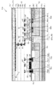
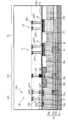
- FIG. 6 shows a schematic plan view of the pixel 110B according to the second embodiment.
- FIG. 7 is a schematic cross-sectional view of pixel 110B.
- FIG. 6 schematically shows the arrangement of each element provided on the semiconductor substrate 60 when the pixel 110B shown in FIG. 7 is viewed along the normal direction of the semiconductor substrate 60.
- the cross section shown in FIG. 7 is developed by cutting the pixel 110B along the VII-VII broken line in FIG. In FIG. 6, some elements are not shown.
- the pixel 110B includes a semiconductor substrate 60, a photoelectric conversion unit 17, a conductive structure 89, and an interlayer insulating layer 90.
- the conductive structure 89 is arranged above the semiconductor substrate 60. Specifically, the conductive structure 89 is arranged on the incident side of light when viewed from the semiconductor substrate 60.
- the semiconductor substrate 60 includes a support substrate 61, a P-type semiconductor region 61p, a P-well 65p, an N-well 65n, a diffusion region 67n, a diffusion region 68an, a diffusion region 68bn, a diffusion region 72ap, and a diffusion region 72bp. And the element separation region 69a and the element separation region 69b.
- the support substrate 61 is a P-type substrate. Specifically, the support substrate 61 is a P-type silicon substrate.
- the P-type semiconductor region 61p is arranged on the support substrate 61.
- the P-type semiconductor region 61p contains P-type impurities at a concentration lower than that of the support substrate 61.
- the P-well 65p is arranged in the P-type semiconductor region 61p.
- the P-well 65p contains P-type impurities at a concentration lower than that of the support substrate 61 and higher than that of the P-type semiconductor region 61p.
- the N well 65n is arranged in the P-type semiconductor region 61p.
- N-well 65n contains N-type impurities.
- the P well is a P-type impurity region.
- the N-well is an N-type impurity region.
- the “IMS Tr. Region” is a region in which the P well 65p expands in a plan view.
- the “MOSFET Tr. Region” is a region in which N wells 65n expand in a plan view.
- an insulating layer 70 is provided on the semiconductor substrate 60. Specifically, the insulating layer 70 covers a wide area on the semiconductor substrate 60.
- the reset transistor 400 includes a diffusion region 67n as one of a source and a drain.
- the reset transistor 400 includes a diffusion region 68 bn as the other of the source and drain.
- the reset transistor 400 includes an insulating layer 70 and a gate electrode 400e.
- the gate electrode 400e is provided on the insulating layer 70.
- the diffusion region 67n is also a charge storage unit FD.
- the diffusion region 67n temporarily stores the signal charge generated by the photoelectric conversion unit 17.
- the electric charge storage unit FD and the gate electrode 200e of the amplification transistor 200 are electrically connected to each other by a thick line.
- the feedback transistor 301 includes a diffusion region 68an as one of a source and a drain.
- the feedback transistor 301 includes a diffusion region 68 bn as the other of the source and drain.
- the feedback transistor 301 includes an insulating layer 70 and a gate electrode 301e.
- the gate electrode 301e is provided on the insulating layer 70.
- the inverting transistor 600 includes a diffusion region 72bp as one of a source and a drain.
- the inverting transistor 600 includes a diffusion region 72ap as the other of the source and drain.
- the inverting transistor 600 includes an insulating layer 70 and a gate electrode 600.
- the gate electrode 600 is provided on the insulating layer 70.
- Diffusion regions 67n, 68an and 68bn are N-type impurity regions.
- Diffusion regions 72ap and 72bp are P-type impurity regions.
- the diffusion region 67n is arranged in the P-type semiconductor region 61p.
- the diffusion region 67n includes a first region 67a and a second region 67b.
- the second region 67b is provided in the first region 67a.
- the second region 67b has a higher impurity concentration than the first region 67a.
- the diffusion regions 68an and 68bn are arranged in the P well 65p.
- Diffusion regions 72ap and 72bp are located within N wells 65n.
- the inverting transistor 600 is a MOSFET.
- the amplification transistor 200, the feedback transistor 301, the reset transistor 400, and the selection transistor 503 are NMOSs.
- the element separation region 69a electrically separates the inverting transistor 600, which is a MOSFET, from the amplification transistor 200, the feedback transistor 301, the reset transistor 400, and the selection transistor 503, which are NMOSs.
- the device separation region 69a is a region formed by injection separation.
- the device separation region 69a is an N-type impurity region.
- the device separation region 69a is an N-type impurity region having an impurity concentration higher than that of the N-well 65n.
- the element separation region 69b electrically separates the amplification transistor 200, the feedback transistor 301, the reset transistor 400, and the selection transistor 503, which are NMOSs, from the inverting transistor 600, which is a MOSFET.
- the device separation region 69b is a region formed by injection separation.
- the device separation region 69b is a P-type impurity region.
- the device separation region 69b is a P-type impurity region having an impurity concentration higher than that of the P-well 65p.
- the interlayer insulating layer 90 covers the semiconductor substrate 60.
- the interlayer insulating layer 90 supports the photoelectric conversion unit 17.
- a conductive structure 89 is arranged inside the interlayer insulating layer 90.
- the interlayer insulating layer 90 includes a plurality of insulating layers 90a, 90b, 90c and an insulating layer 90d.
- the number of insulating layers included in the interlayer insulating layer 90 is not particularly limited.
- the conductive structure 89 includes a plurality of wiring layers 80a, 80b and 80c.
- the conductive structure 89 includes a plurality of plugs pa1, pa2, pa3, pa4, pa5, pa6, pa7, pa8, pb, pc, pd, cg1, cg3 and cg5.
- a plug refers to a component used to connect elements.
- the material and structure of the plug are not particularly limited.
- the plug is a concept that includes a direct connection plug, a via plug, and a contact plug.
- the materials and structures of the direct connection plug, the via plug and the contact plug may be the same or different from each other.
- the direct connection plug is a plug that is directly connected to the wiring layer, and refers to a plug that is used to electrically connect the wiring layer to an element located on the semiconductor substrate side of the wiring layer.
- the direct connection plug is directly connected to the wiring layer closest to the semiconductor substrate.
- specific examples of "elements located closer to the semiconductor substrate than the wiring layer" regarding the electrical connection destination of the direct connection plug are a gate electrode, a contact plug, a diffusion region, or a conductive layer.
- An example of the material of the direct connection plug is a metal such as copper (Cu) or tungsten (W). In the illustrated example, the material of the direct plug is tungsten.
- the via plug refers to a plug that electrically connects the wiring layer and the wiring layer, or a plug that is used to electrically connect the wiring layer to an element located on the photoelectric conversion part side of the wiring layer.
- a specific example of the above-mentioned "via plug used for electrically connecting the wiring layer to an element located closer to the photoelectric conversion unit than the wiring layer” is that the wiring layer closest to the pixel electrode is electrically connected to the pixel electrode. Connect to.
- a via plug material is a metal such as copper (Cu) or tungsten (W).
- a specific example of the material for the via plug is copper.
- the contact plug is a plug containing impurities of the first conductive type or the second conductive type.
- the first conductive type and the second conductive type are different conductive types from each other.
- the first conductive type is N type or P type.
- the second conductive type is P type or N type.
- the contact plug is connected to, for example, a diffusion region or a gate electrode.
- the contact plug is interposed between the directly connected plug and the diffusion region or between the directly connected plug and the gate electrode in the pixel.
- the contact plug is interposed between the first element and the second element to realize a contact resistance between the first element and the contact plug, which is lower than the default resistance.
- it refers to a plug that is the contact resistance between the second element and the contact plug and realizes a contact resistance lower than the default resistance.
- the default resistance is the contact resistance between the first element and the second element when the first element and the second element are directly connected.
- the contact plug realizes low contact resistance by being interposed between the directly connected plug as the first element and the diffusion region as the second element.
- An example of a contact plug material is polysilicon.
- the plugs pb, pc and pd are via plugs.
- the plugs pa1, pa2, pa3, pa4, pa5, pa6, pa7, and pa8 are directly connected plugs.
- the plugs cg1, cg3 and cg5 are contact plugs.
- the plugs cg1, cg3 and cg5 have a film-shaped portion.
- the number of wiring layers included in the conductive structure 89 is not particularly limited.
- the number of plugs included in the conductive structure 89 is not particularly limited.
- the plurality of wiring layers may include a part or all of the band control signal line CON1, the reset control signal line CON2, and the selection control signal line CON3.
- the plugs cg1, cg3, cg5, pa1, pa2, pa3, pa4, pa5, pa6, pa7 and pa8 are arranged in the insulating layer 90a.
- the wiring layer 80a is arranged in the insulating layer 90a.
- the plug pb and the wiring layer 80b are arranged in the insulating layer 90b.
- the plug pc and the wiring layer 80c are arranged in the insulating layer 90c.
- the plug pd is arranged in the insulating layer 90d.
- the wiring layer 80a is electrically connected to the diffusion region 68an via the plug pa1 and the plug cg1 in this order.
- the wiring layer 80a is electrically connected to the diffusion region 68bn via the plug pa3 and the plug cg3 in this order.
- the wiring layer 80a is electrically connected to the diffusion region 72ap via the plug pa6.
- the wiring layer 80a is electrically connected to the diffusion region 72bp via the plug pa8.
- the diffusion region 68an includes a first region 68an1 and a second region 68an2.
- the second region 68an2 is provided in the first region 68an1.
- the second region 68an2 has a higher impurity concentration than the first region 68an1.
- the plug cg1 is connected to the second region 68an2.
- the diffusion region 68bn includes a first region 68bn1 and a second region 68bn2.
- the second region 68bn2 is provided in the first region 68bn1.
- the second region 68bn2 has a higher impurity concentration than the first region 68bn1.
- the plug cg3 is connected to the second region 68bn2.
- the wiring layer 80a is electrically connected to the gate electrode 301e via the plug pa2.
- the wiring layer 80a is electrically connected to the gate electrode 400e via the plug pa4.
- the wiring layer 80a is electrically connected to the gate electrode 600e via the plug pa7.
- the pixel electrode 17a is electrically connected to the diffusion region 67n, that is, the charge storage portion FD via the conductive structure 89. Specifically, the pixel electrode 17a passes through the plug pd, the wiring layer 80c, the plug pc, the wiring layer 80b, the plug pb, the wiring layer 80a, the plug pa5, and the plug cg5 in this order. It is electrically connected to the diffusion region 67n. Specifically, the plug cg5 is connected to the second region 67b of the diffusion region 67n.
- the wiring layers 80a, 80b and 80c are formed of a metal such as copper or tungsten, or a metal compound such as a metal nitride or a metal oxide.
- a metal such as copper or tungsten
- a metal compound such as a metal nitride or a metal oxide.
- the number of electric paths connecting the wiring layer 80a and the diffusion region 72ap is one, and specifically, the electric paths are configured by one plug.
- the number of parallel electric paths connecting the wiring layer 80a and the diffusion region 72ap may be plural, and specifically, such parallel electric paths may be configured by a plurality of plugs. In this way, the contact resistance between the electric paths and the diffusion region 72ap can be reduced as compared with the case where the number of electric paths is one. This can improve the performance of the characteristic transistor 600. The same applies to the number of electric paths connecting the wiring layer 80a and the diffusion region 72bp.
- the plugs (specifically, contact plugs) cg1, cg3 and cg5 are formed of polysilicon. Therefore, the conductivity of the plugs cg1, cg3 and cg5 can be increased, and the contact resistance between the plugs cg1, cg3 and cg5 and the diffusion regions 68an, 68bn and 67n can be reduced. This can improve the performance of the feedback transistor 301 and the reset transistor 400.
- the plugs cg1, cg3 and cg5 are N-type polysilicon plugs doped with N-type impurities.
- the N-type impurity is, for example, phosphorus.
- the plugs cg1, cg3 and cg5, and the gate electrodes 301e and 400e also have a film-shaped portion. Also, they are made of the same material. This means that these can be formed by a common film forming process, which is advantageous from the viewpoint of simplifying the manufacturing process.
- the plugs cg1, cg3 and cg5 and the gate electrodes 301e and 400e are formed of polysilicon.
- the photoelectric conversion unit 17 is a photoelectric conversion unit 17A including a pixel electrode 17a, a counter electrode 17c, and a photoelectric conversion layer 17b.
- the pixel electrode 17a is provided on the interlayer insulating layer 90. Specifically, the pixel electrode 17a is provided on the insulating layer 90d.
- the counter electrode 17c is arranged on the incident side of the light.
- the photoelectric conversion layer 17b is arranged between the pixel electrode 17a and the counter electrode 17c.
- the counter electrode 17c has a connection with the above-mentioned storage control line 130.
- the potential of the storage control line 130 is controlled to make the potential of the counter electrode 17c higher than the potential of the pixel electrode 17a.
- the positive charge among the positive and negative charges generated by the photoelectric conversion can be selectively collected by the pixel electrode 17a.
- the counter electrode 17c is a single layer continuous over the plurality of pixels 110B, it is possible to collectively apply a predetermined potential to the counter electrodes 17c of the plurality of pixels 110B.
- the pixel electrode 17a is electrically connected to the diffusion region 67n, that is, the charge storage portion FD via the conductive structure 89. Therefore, the electric charge collected by the pixel electrode 17a is transmitted to the diffusion region 67n via the conductive structure 89.
- the pixel electrode 17a passes through the plug pd, the wiring layer 80c, the plug pc, the wiring layer 80b, the plug pb, the wiring layer 80a, the plug pa5, and the plug cg5 in this order. It is electrically connected to the diffusion region 67n. Therefore, the electric charge collected by the pixel electrode 17a is transmitted to the diffusion region 67n via these in this order.
- the present embodiment will be further described using the terms such as the first transistor and the second transistor.
- the pixel 110B includes a photoelectric conversion unit 17, a charge storage unit FD, an amplification transistor 200 which is a first transistor, and an inverting transistor 600 which is a second transistor.
- the photoelectric conversion unit 17 converts light into electric charges.
- the charge storage unit FD stores the electric charge generated by the photoelectric conversion unit 17.
- the charge storage unit FD is a first conductive type diffusion region.
- the first transistor includes a source or drain containing first conductive type impurities.
- the second transistor includes a source or drain containing a second conductive type impurity.
- the second conductive type is different from the first conductive type.
- the conductive type differs between the charge storage unit FD and the source or drain of the second transistor.
- the source or drain of the second transistor may affect the charge storage unit FD.
- One example of the effect is the diffusion of conductive impurities different from the impurities contained in the charge storage unit FD from the second transistor to the charge storage unit FD.
- Another example of the effect is the influx of parasitic carriers generated in the second transistor from the second transistor into the charge storage section FD. As the pixel size shrinks, this effect is more likely to become apparent. This effect can cause leak currents and increase noise. Noise can degrade the image.
- the distance D2 between the charge storage unit FD and the inverting transistor 600, which is the second transistor, is the charge storage unit FD and the amplification transistor 200, which is the first transistor. Distance is longer than D1. Therefore, the above-mentioned influence can be suppressed. Therefore, this embodiment is suitable for reducing noise and obtaining a high-quality image.
- planar view means observing in a direction perpendicular to the surface of the semiconductor substrate 60.
- FIG. 6 represents the pixel 110B in a plan view.
- the distance D2 is the minimum distance between the charge storage unit FD and the source or drain of the inverting transistor 600, which is the second transistor, in a plan view.
- the distance D1 is the minimum distance between the charge storage unit FD and the gate electrode of the amplification transistor 200, which is the first transistor, in a plan view.
- FIG. 6 shows the distance D2 and the distance D1 in the first example.
- the outer edge of the diffusion region such as the source, drain, and charge storage portion FD is defined by a junction in which the concentration of the first conductive type impurity and the concentration of the second conductive type impurity are equal.
- the distance D2 is the distance between the centers of the charge storage unit FD and the source or drain of the inverting transistor 600, which is the second transistor, in a plan view.
- the distance D1 is the distance between the centers of the charge storage unit FD and the gate electrode of the amplification transistor 200, which is the first transistor, in a plan view.
- the center refers to the geometric center.
- the distance D2 is a connection portion between the charge storage portion FD and the conductive structure 89 and a connection portion between the source or drain of the inverting transistor 600 which is the second transistor and the conductive structure 89 in a plan view.
- the distance D1 is the distance between the connection portion between the charge storage portion FD and the conductive structure 89 and the connection portion between the gate electrode of the amplification transistor 200, which is the first transistor, and the conductive structure 89 in a plan view.
- the distance D2 is the distance between the centers of the charge storage unit FD and the gate electrode of the inverting transistor 600, which is the second transistor, in a plan view.
- the distance D1 is the distance between the centers of the charge storage unit FD and the gate electrode of the amplification transistor 200, which is the first transistor, in a plan view.
- the center refers to the geometric center.
- the distance D2 when the distance D2 is larger than the distance D1 in the plan view in any of the first example, the second example, the third example, and the fourth example, the distance D2 is larger than the distance D1 in the plan view. Will be treated as.
- the charge storage unit FD, the amplification transistor 200 which is the first transistor, and the inverting transistor 600 which is the second transistor are provided on a single semiconductor substrate 60.
- the above effects are likely to become apparent. Therefore, in the present embodiment, the effect of suppressing the above-mentioned influence is effectively exhibited by the magnitude relationship between the distances D2 and D1.
- the first transistor is an amplification transistor 200.
- the amplification transistor 200 generates a signal corresponding to the charge stored in the charge storage unit FD.
- the second transistor is an inverting transistor 600.
- the amplification transistor 200 which is the first transistor, is electrically connected to the charge storage unit FD.
- the gate of the first transistor is electrically connected to the charge storage unit FD.
- the inverting transistor 600 which is the second transistor, may also be electrically connected to the charge storage unit FD.
- the amplification transistor 200 which is the first transistor, is located in the first central region, which is the central region of the pixel 110B.
- the distance D2 can be easily made larger than the distance D1 in the plan view.
- the first central region of a pixel in plan view is a region similar to a pixel in plan view, the area is 70% of the area of the pixel, and the geometric center is the same as the geometric center of the pixel. It means a certain area.
- the amplification transistor 200 which is the first transistor, may be located in the second central region of the pixel 110B.
- the second central region of a pixel in plan view is a region similar to a pixel in plan view, the area is 40% of the area of the pixel, and the geometric center is the same as the geometric center of the pixel. means.
- the amplification transistor 200 which is the first transistor, may be located in the third central region of the pixel 110B.
- the third central region of a pixel in plan view is a region similar to a pixel in plan view, the area is 10% of the area of the pixel, and the geometric center is the same as the geometric center of the pixel. means.
- the outer edge of a pixel can be understood from, for example, a repeating array of pixels.
- a pixel is the smallest unit that can express gradation.
- the charge storage unit FD and the inverting transistor 600 which is the second transistor, are located on opposite sides of the amplification transistor 200, which is the first transistor, with respect to the CD1 in a certain direction.
- the charge storage unit FD, the first transistor, and the second transistor are arranged in this order with respect to the CD1 in a certain direction. In this way, the distance D2 can be easily made larger than the distance D1 in the plan view.
- the direction CD1 is the row direction.
- the direction CD1 may be in the column direction.
- the first conductive type is N type.
- the second conductive type is a P type.
- the amplification transistor 200 includes a source or drain containing N-type impurities. In this case, it is easier to secure the transconductance of the amplification transistor 200 as compared with the case where the amplification transistor 200 contains a source or drain containing P-type impurities. This is because electrons have higher mobility than holes. It is advantageous from the viewpoint of ensuring the performance of the amplification transistor 200 that it is easy to secure the transconductance.
- the pixel 110B has a first well region 65p and a second well region 65n.
- the first well region 65p contains a second conductive type impurity.
- the amplification transistor 200 which is the first transistor, is located in the first well region 65p.
- the second well region 65n contains first conductive type impurities.
- An inverting transistor 600 which is a second transistor, is located in the second well region 65n.
- the area of the first well region 65p is larger than the area of the second well region 65n.
- the area of the first well region 65p belonging to the pixel 110B is larger than the area of the second well region 65n belonging to the pixel 110B.
- the first well region 65p is a P well 65p.
- the second well region 65n is an N well region 65n.
- the image pickup apparatus 100 has a semiconductor substrate 60.
- this cross section may be referred to as, for example, a first cross section
- the source or drain of the amplification transistor 200 which is the first transistor
- the inverting transistor which is the second transistor. With 600 sources or drains, appears.
- the source or drain of the first transistor means at least one of the source and drain of the first transistor. The same applies to the source or drain of the second transistor.
- the source and drain of the first transistor and the source and drain of the second transistor appear.
- the charge storage portion FD also appears.
- the pixel 110B has an element separation region 69a and an element separation region 69b.
- the element separation region 69a separates the inverting transistor 600, which is the second transistor, from other elements.
- the element separation region 69b separates the reset transistor 400 whose polarity is inverted from that of the second transistor from other elements.
- the element separation region 69a and the element separation region 69b are formed by injection separation.
- the arrangement of the elements shown in the plan view of FIG. 6 can be applied to other embodiments.
- the element can be added to the plan view of FIG.
- the element can be eliminated from the plan view of FIG.
- the selection transistor 503 can be eliminated from the plan view of FIG. 6, and the selection transistor 502 can be used as the inverting transistor 600 to make other modifications.
- FIG. 8 shows a plan view applicable to the first embodiment.
- FIG. 9 is a schematic cross-sectional view of the pixel 110C.
- the conductive structure 89 includes a plurality of plugs cp1, cp2, cp3, cp4, cp5, cp6, cp7 and cp8. These plugs are arranged in the insulating layer 90a. These plugs have a rod-shaped portion. These plugs are specifically contact plugs.
- the wiring layer 80a is electrically connected to the diffusion region 68an via the plugs pa1 and cp1 in this order.
- the wiring layer 80a is electrically connected to the diffusion region 68bn via the plugs pa3 and cp3 in this order.
- the wiring layer 80a is electrically connected to the diffusion region 72ap via the plugs pa6 and cp6 in this order.
- the wiring layer 80a is electrically connected to the diffusion region 72bp via the plugs pa8 and cp8 in this order.
- the plug cp1 is connected to the second region 68an2 of the diffusion region 68an. Further, the plug cp3 is connected to the second region 68bn2 of the diffusion region 68bn.
- the diffusion region 72ap includes a first region 72ap1 and a second region 72ap2.
- the second region 72ap2 is provided in the first region 72ap1.
- the second region 72ap2 has a higher impurity concentration than the first region 72ap1.
- the plug cp6 is connected to the second region 72ap2.
- the diffusion region 72bp includes the first region 72bp1 and the second region 72bp2.
- the second region 72bp2 is provided in the first region 72bp1.
- the second region 72bp2 has a higher impurity concentration than the first region 72bp1.
- the plug cp8 is connected to the second region 72bp2.
- the wiring layer 80a is electrically connected to the gate electrode 301e via the plugs pa2 and cp2 in this order.
- the wiring layer 80a is electrically connected to the gate electrode 400e via the plugs pa4 and cp4 in this order.
- the wiring layer 80a is electrically connected to the gate electrode 600e via the plugs pa7 and cp7 in this order.
- the pixel electrode 17a is electrically connected to the diffusion region 67n, that is, the charge storage portion FD via the conductive structure 89. Specifically, the pixel electrode 17a passes through the plug pd, the wiring layer 80c, the plug pc, the wiring layer 80b, the plug pb, the wiring layer 80a, the plug pa5, and the plug cp5 in this order. It is electrically connected to the diffusion region 67n.
- the plugs (specifically, contact plugs) cp1, cp2, cp3, cp4, cp5, cp6, cp7 and cp8 are formed of polysilicon. Therefore, the conductivity of the plugs cp1, cp3, cp5, cp6 and cp8 can be increased, and the contact resistance between the plugs cp1, cp3, cp5, cp6 and cp8 and the diffusion regions 68an, 68bun, 67n, 72ap and 72bp can be reduced. ..
- the conductivity of the plugs cp2, cp4 and cp7 can be increased, and the contact resistance between the plugs cp2, cp4 and cp7 and the gate electrodes 301e, 400e and 600e can be reduced. This can improve the performance of the feedback transistor 301, the reset transistor 400 and the inverting transistor 600.
- the plurality of plugs cp1, cp2, cp3, cp4 and cp5 are N-type polysilicon plugs doped with N-type impurities.
- the N-type impurity is, for example, phosphorus.
- the plurality of plugs cp6, cp7 and cp8 are P-type polysilicon plugs doped with P-type impurities.
- the P-type impurity is, for example, boron.
- FIG. 10 shows a configuration example applicable to the pixel 110C.
- the configuration of FIG. 10 is also applicable to other embodiments.
- the region xp is a combination of the P-type semiconductor region 61p and the P-well 65p.
- the insulating layer 71 is provided so as to cover the gate electrodes 400e and 600e.
- the insulating layer 71 is, for example, a silicon oxide film.
- the insulating layer 71 may have a laminated structure.
- a sidewall 75 is provided on the insulating layer 71.
- the sidewall 75 is, for example, a silicon nitride film.
- the sidewall 75 is arranged between the plug cp3 and the gate electrode 400e.
- the sidewall 75 is arranged between the plug cp5 and the gate electrode 400e.
- the sidewall 75 is arranged between the plug cp5 and the plug cp6.
- the sidewall 75 is arranged between the plug cp6 and the gate electrode 600e.
- the sidewall 75 is arranged between the plug cp8 and the gate electrode 600e.
- the sidewall 75 overlaps with the diffusion region 68bn. In plan view, the sidewall 75 overlaps the diffusion region 67n. In plan view, the sidewall 75 overlaps with the diffusion region 72ap. In plan view, the sidewall 75 overlaps the diffusion region 72bp.
- Overlapping of two elements in plan view means that the two elements have at least partial overlap in plan view.
- the damage is, for example, the damage caused by the plasma used in the process after the formation of the diffusion region.
- Plasma damage is, for example, physical damage due to accelerated ion collisions and the creation of defects due to light.
- Light is, for example, ultraviolet light.
- the sidewall may be placed between the other plug and the gate electrode.
- the sidewalls may be arranged so as to overlap other diffusion regions in a plan view.
- the insulating layer 70 and the insulating layer 71 have a plurality of contact holes h3, h5, h6 and h8. These contact holes penetrate the insulating layer 70 and the insulating layer 71.
- the contact hole h3 overlaps with the diffusion region 68bn.
- a plug cp3 is arranged in the contact hole h3.
- the contact hole h5 overlaps with the diffusion region 67n.
- a plug cp5 is arranged in the contact hole h5.
- the contact hole h6 overlaps with the diffusion region 72ap.
- a plug cp6 is arranged in the contact hole h6.
- the contact hole h8 overlaps with the diffusion region 72bp.
- a plug cp8 is arranged in the contact hole h8.
- a contact hole may be formed at a position overlapping with another diffusion region in a plan view, and a plug may be placed in the contact hole.
- FIG. 11 is a schematic cross-sectional view of the pixel 110D.
- the conductive structure 89 includes a plurality of plugs cg6 and cg8.
- the plugs cg6 and cg8 are arranged in the insulating layer 90a.
- the plugs cg6 and cg8 have a film-shaped portion. Further, the plugs cg6 and cg8 are contact plugs.
- the wiring layer 80a is electrically connected to the diffusion region 72ap via the plug pa6 and the plug cg6 in this order.
- the wiring layer 80a is electrically connected to the diffusion region 72bp via the plug pa8 and the plug cg8 in this order.
- the plug cg6 is connected to the second region 72ap2 of the diffusion region 72ap. Further, the plug cg8 is connected to the second region 72bp2 of the diffusion region 72bp.
- the plugs cg6 and cg8 are formed of polysilicon. Therefore, the conductivity of the plugs cg6 and cg8 can be increased, and the contact resistance between the plugs cg6 and cg8 and the diffusion regions 72ap and 72bp can be reduced. This can improve the performance of the inverting transistor 600.
- the plurality of plugs cg6 and cg8 are P-type polysilicon plugs doped with P-type impurities.
- the P-type impurity is, for example, boron.
- both the plugs cg6 and cg8 and the gate electrode 600e have a film-shaped portion. Also, they are made of the same material. This means that these can be formed by a common film forming process, which is advantageous from the viewpoint of simplifying the manufacturing process. Specifically, the plugs cg6 and cg8 and the gate electrode 600e are formed of polysilicon.
- the third embodiment and the fourth embodiment will be further described using the terms such as the first transistor and the second transistor.
- Pixels 110C and 110D include a reset transistor 400 which is a first transistor, an inverting transistor 600 which is a second transistor, a first contact plug, and a second contact plug.
- the first transistor includes a diffusion region 67n or 68bn corresponding to a first diffusion region which is a source or drain, and a gate electrode 400e which is a first gate electrode containing a first conductive type impurity.
- the second transistor includes a diffusion region 72ap or 72bp corresponding to a second diffusion region which is a source or drain, and a second gate electrode 600e containing impurities of a second conductive type different from the first conductive type.
- the first contact plug is connected to the diffusion region 67n or 68bn, which is the first diffusion region, and contains the first conductive type impurities.
- the second contact plug is connected to the diffusion region 72ap or 72bp, which is the second diffusion region, and contains a second conductive type impurity.
- Both the gate electrode 400e, which is the first gate electrode, and the first contact plug are parts that contribute to the operation of the reset transistor 400, which is the first transistor.
- both of these portions contain first conductive type impurities. Doing so can contribute to ensuring the stability of operation of the first transistor. For example, when mass-producing an imaging device, quality variations are less likely to occur. This leads to obtaining a high-quality image. The same can be said for the configuration of the inverting transistor 600, which is the second transistor.
- the first contact plug is a plug cp3 or cp5.
- the second contact plug is a plug cp6 or cp8.
- the first contact plug is a plug cg3 or cg5.
- the second contact plug is a plug cg6 or cg8.
- the diffusion region 67n or 68bn which is the first diffusion region, contains the first conductive type impurities.
- the diffusion region 72ap or 72bp, which is the second diffusion region, contains a second conductive type impurity.
- the conductive type of the impurities in the first contact plug and the first diffusion region connected to each other is the same in the first conductive type.
- the conductive type of impurities in the second contact plug and the second diffusion region connected to each other is the same in the second conductive type. This is advantageous from the viewpoint of reducing the contact resistance between the first contact plug and the first diffusion region and improving the performance of the first transistor. It is also advantageous from the viewpoint of reducing the contact resistance between the second contact plug and the second diffusion region and improving the performance of the second transistor. These are advantageous from the viewpoint of obtaining a high-quality image.
- the first diffusion region includes a first region having a relatively low impurity concentration and a second region provided in the first region having a relatively high impurity concentration. Have. Then, the first contact plug is connected to the second region of the first diffusion region. In this case, the effect of reducing the contact resistance based on the first contact plug is likely to be effectively exhibited.
- the second diffusion region includes a first region having a relatively low impurity concentration and a second region provided in the first region having a relatively high impurity concentration.
- a second contact plug is connected to the second region of the second diffusion region. In this case, the effect of reducing the contact resistance based on the second contact plug is likely to be effectively exhibited.
- the first diffusion region is the charge storage unit FD.
- the charge storage unit FD stores charges.
- the first transistor is a reset transistor 400.
- the reset transistor 400 resets the charge storage unit FD.
- the second transistor is an inverting transistor 600.
- the first region of the first diffusion region is the first region 67a of the charge storage unit FD.
- the second region of the first diffusion region is the second region 67b of the charge storage unit FD.
- the first region of the second diffusion region is the first region 72ap1 or 72bp1.
- the second region of the second diffusion region is the second region 72ap2 or 72bp2.
- the first conductive type is N type.
- the second conductive type is P type.
- FIG. 12 is a schematic cross-sectional view of the pixel 110E.
- the element separation region 69c is used instead of the element separation region 69a.
- the element separation region 69c has an STI (Shallow Trench Isolation) structure.
- the element separation function can be easily secured even if the impurity concentration in the source and drain of the inverting transistor 600 is high. This is advantageous from the viewpoint of reducing the contact resistance between the plugs cg6 and cg8 and the diffusion regions 72ap and 72bp. This can improve the performance of the inverting transistor 600.
- the high element separation function based on the STI structure can also contribute to the reduction of pixel size.
- the plugs cg6 and cg8 are specifically contact plugs.
- the element separation region 69b is a region formed by injection separation.
- the device separation region 69c having the STI structure and the device separation region 69b formed by injection separation may be combined.
- the device separation region 69c having an STI structure is formed of, for example, a silicon oxide.
- the fifth embodiment will be further described using the terms such as the first transistor and the second transistor.
- Pixel 110E has an element separation region 69c.
- the element separation region 69c separates the second transistor 600 into elements.
- the element separation region 69c has an STI structure.
- the STI structure may have crystal defects on its side wall. Crystal defects can add noise to the charge storage section FD.
- the distance D3 between the charge storage unit FD and the element separation region 69c is longer than the distance D1 between the charge storage unit FD and the amplification transistor 200, which is the first transistor, in a plan view. This suppresses the generation of noise due to crystal defects in the charge storage portion FD, and is suitable for obtaining a high-quality image.
- the element separation region 69c is a region formed by injection separation, making the distance D3 longer than the distance D1 can contribute to the improvement of image quality. By doing so, it is possible to suppress the generation of noise due to high-concentration impurities in the injection separation region in the charge storage portion FD.
- the distance D3 is the minimum distance between the charge storage portion FD and the element separation region 69c in a plan view.
- the distance D1 is the minimum distance between the charge storage unit FD and the gate electrode of the amplification transistor 200, which is the first transistor, in a plan view.
- the element separation region 69c separates the inverting transistor 600, which is the second transistor, from the amplification transistor 200, which is the first transistor.
- a structure for suppressing a leak current between the element is provided between the element and the other element.
- the fact that an element is separated from another element means that, in plan view, the element is surrounded by the above structure and the other element is arranged outside the structure.
- Pixel 110E has an element separation region 69b.
- the element separation region 69b separates the reset transistor 400 whose polarity is inverted from that of the inverting transistor 600, which is the second transistor, from other elements.
- the element separation region 69c is formed by injection separation.
- the charge storage unit FD and the element separation region 69c are located on opposite sides of each other when viewed from the amplification transistor 200, which is the first transistor, in a certain direction. In this way, the distance D3 can be easily made longer than the distance D1 in a plan view.
- FIG. 13 is a schematic cross-sectional view of the pixel 110F.
- Pixel 110F has an N-type semiconductor region 62n.
- the N-type semiconductor region 62n divides the P-type semiconductor region 61p into a first region 61p1 in which the diffusion region 67n is arranged and a second region 61p2 different from the first region 61p1.
- the N-type semiconductor region 62n can suppress the inflow of minority carriers generated in the inverting transistor 600 or peripheral circuits into the charge storage unit FD. This is suitable for suppressing the leakage current due to the inflow of a small number of carriers into the charge storage portion FD and obtaining a high-quality image.
- the support substrate 61, the second region 61p2, the N-type semiconductor region 62n, and the first region 61p1 are arranged in this order. Further, the support substrate 61, the second region 61p2, the N-type semiconductor region 62n, and the P well 65p are arranged in this order.
- the second region 61p2 overlaps the P well 65p and the N well 65n. In a plan view, the second region 61p2 overlaps the charge storage unit FD. Further, in a plan view, the second region 61p2 overlaps at least one of the diffusion regions 72ap and 72bp, specifically both.
- Pixel 110F has at least one P-shaped region 64. Specifically, the pixel 110F has a plurality of P-shaped regions 64.
- the P-type region 64 has a higher impurity concentration than the support substrate 61 and the P-type semiconductor region 61p.
- the P-type region 64 electrically connects the support substrate 61, the P-type semiconductor region 61p, and the P-well 65p.
- the sixth embodiment will be further described using the terms such as the first semiconductor region and the second semiconductor region.
- the pixel 110F has a P-type semiconductor region 61p, which is a first semiconductor region, and an N-type semiconductor region 62n, which is a second semiconductor region.
- the second semiconductor region divides the first semiconductor region into a first region 61p1 and a second region 61p2 different from the first region 61p1.
- a charge storage unit FD is arranged in the first region 61p1. In a plan view, the second region 61p2 overlaps with the second well region N well 65n.
- the second region 61p2 overlapping the second well region in the plan view and the first region 61p1 in which the charge storage portion FD is arranged are the N-type semiconductor region which is the second semiconductor region. It is partitioned by 62n. Therefore, in this embodiment, it is possible to suppress the inflow of minority carriers generated in the inverting transistor 600, which is the second transistor, into the charge storage unit FD. This is suitable for suppressing the leakage current due to the inflow of a small number of carriers into the charge storage portion FD and obtaining a high-quality image.
- the first semiconductor region is the P-type semiconductor region 61p.
- the second semiconductor region is an N-type semiconductor region 62n.
- the second well region is the N well region 65n.
- the charge storage unit FD corresponds to the diffusion region 67n.
- FIG. 14 shows a schematic plan view of the pixel 110G according to the seventh embodiment.
- FIG. 15 shows a schematic cross-sectional view of the pixel 110G.
- FIG. 14 schematically shows the arrangement of each element provided on the semiconductor substrate 60 when the pixel 110G shown in FIG. 15 is viewed along the normal direction of the semiconductor substrate 60.
- the cross section shown in FIG. 15 is developed by cutting the pixel 110G along the XV-XV broken line in FIG.
- the conductive structure 89 includes plugs pa0, pa9, cg0 and cg9.
- the semiconductor substrate 60 includes a sub-contact region 66p and a well contact region 66n.
- the plugs pa0 and pa9 are directly connected plugs.
- the plugs cg0 and cg9 have a film-shaped portion. Further, the plugs cg0 and cg9 are contact plugs.
- the sub-contact region 66p has P-type impurities.
- the sub-contact region 66p is arranged within the P-well 65p.
- the sub-contact region 66p may be formed on the P-type element separation region.
- An element separation region 69b is arranged between the sub-contact region 66p and the diffusion region 68an.
- the well contact region 66n has N-type impurities.
- the well contact region 66n is arranged within the N well 65n.
- An element separation region 69c is arranged between the well contact region 66n and the diffusion region 72bp.
- the plugs pa0, pa9, cg0 and cg9 are arranged in the insulating layer 90a.
- the wiring layer 80a is electrically connected to the sub-contact region 66p via the plug pa0 and the plug cg0 in this order.
- the wiring layer 80a is electrically connected to the well contact region 66n via the plug pa9 and the plug cg9 in this order.
- the sub-contact region 66p includes the first region 66p1 and the second region 66p2.
- the second region 66p2 is provided in the first region 66p1.
- the second region 66p2 has a higher impurity concentration than the first region 66p1.
- the plug cg0 is connected to the second region 66p2.
- the well contact region 66n includes a first region 66n1 and a second region 66n2.
- the second region 66n2 is provided in the first region 66n1.
- the second region 66n2 has a higher impurity concentration than the first region 66n1.
- the plug cg9 is connected to the second region 66n2.
- the plugs (specifically, directly connected plugs) pa0 and pa9 are formed of a metal such as copper or tungsten, or a metal compound such as a metal nitride or a metal oxide.
- the plug (specifically, the contact plug) cg0 is formed of polysilicon.
- the plug cg0 is a P-type polysilicon plug doped with P-type impurities.
- the P-type impurity is, for example, boron.
- the plug (specifically, the contact plug) cg9 is formed of polysilicon.
- the plug cg9 is an N-type polysilicon plug doped with N-type impurities.
- the N-type impurity is, for example, phosphorus.
- a voltage can be supplied from the wiring layer 80a to the P well 65p via the plug pa0, the plug cg0, and the sub-contact region 66p in this order.
- a voltage can be supplied from the wiring layer 80a to the N well 65n via the plug pa9, the plug cg9, and the well contact region 66n in this order.
- one sub-contact area 66p and one well contact area 66n are provided for one pixel 110G.
- one sub-contact region 66p and one well contact region 66n may be provided for each of the plurality of pixels 110G.
- the plurality is, for example, four.
- the seventh embodiment will be further described using the terms such as the first well region and the second well region.
- the pixel 110G includes a P-well 65p which is a first well region, an N-well 65n which is a second well region, a sub-contact region 66p which is a first contact region, and a well contact region 66n which is a second contact region.
- the first well region contains a second conductive type impurity.
- the amplification transistor 200 which is the first transistor, is located in the first well region.
- the second well region contains first conductive type impurities.
- An inverting transistor 600 which is a second transistor, is located in the second well region.
- the first contact region contains a second conductive type impurity.
- the second contact region contains first conductive type impurities.
- a voltage is supplied to the first well region via the first contact region.
- a voltage is supplied to the second well region via the second contact region.
- each pixel 110G a voltage is supplied to the first well region via the first contact region.
- a voltage is supplied to the second well region via the second contact region.
- the first well region is a P well 65p.
- the second well region is the N well region 65n.
- the first contact region is a sub-contact region 66p.
- the second contact region is a well contact region 66n.
- the gate 200e of the amplification transistor 200 is located slightly above the center of the pixel 110G.
- the gate 200e of the amplification transistor 200 may be located at the center of the pixel 110G to the same extent as in FIG. 6 and the like in a plan view.
- a pixel array is composed of a plurality of pixels.
- an example of pixel arrangement in the pixel array will be described with reference to FIG.
- the pixel array AR1 in which a plurality of pixels 110B of the second embodiment are arranged will be described.
- a similar pixel array may be configured using the pixels described in other embodiments.
- one of the two pixels 110B adjacent to each other will be referred to as the first pixel 210A.
- the other of the two pixels 110B is referred to as a second pixel 210B.
- the charge storage unit FD of the first pixel 210A, the inverting transistor 600 which is the second transistor of the first pixel 210A, and the second transistor of the second pixel 210B are used for the CD1 in a certain direction.
- a certain inverting transistor 600 and the charge storage unit FD of the second pixel 210B are arranged in this order. In this way, the distance between the second transistor of the first pixel 210A and the charge storage unit FD of the second pixel 210B in the plan view is unlikely to be shortened. Further, in a plan view, the distance between the second transistor of the second pixel 210B and the charge storage unit FD of the first pixel 210A is unlikely to be shortened. This is suitable for obtaining a high-quality image.
- the second pixel 210B has a configuration that is line-symmetrically inverted with respect to the first pixel 210A.
- This inverted arrangement can be referred to as a flip arrangement.
- the second pixel 210B is horizontally inverted with respect to the first pixel 210A.
- the second pixel 210B may be upside down with respect to the first pixel 210A.
- the axis of line symmetry in plan view may extend in the column direction or in the row direction.
- the direction CD1 may be in the row direction or in the column direction.
- the first pixel 210A and the second pixel 210B share one P well 65p, which is a first well region. This is advantageous from the viewpoint of miniaturization of the image pickup apparatus.
- the fact that the first pixel 210A and the second pixel 201B share one first well region means that at least a part of the first well region belongs to the first pixel 210A and at least a part of the first well region is the second. It means that it belongs to pixel 210B.
- the first well region is P well 65p.
- the first pixel 210A and the second pixel 210B may share one second well region, N well 65n. This is advantageous from the viewpoint of miniaturization of the image pickup apparatus.
- the first pixel 210A and the second pixel 201B share one second well region, at least a part of the second well region belongs to the first pixel 210A and at least a part of the second well region is the second. It means that it belongs to pixel 210B.
- the second well region is N well 65n.
- the pixel array AR1 includes the third pixel 210C and the fourth pixel 210D.
- the third pixel 210C and the fourth pixel 210D correspond to the pixel 110B, respectively.
- the second pixel 210B and the third pixel 210C are adjacent to each other.
- the third pixel 210C and the fourth pixel 210D are adjacent to each other.
- the first pixel 210B, the second pixel 210B, the third pixel 210C, and the fourth pixel 210D are arranged in this order.
- the charge storage unit FD of the first pixel 210A, the inverting transistor 600 which is the second transistor of the first pixel 210A, and the second transistor of the second pixel 210B are used for the CD1 in a certain direction.
- the inverting transistor 600, which is a transistor, and the charge storage unit FD of the fourth pixel 210D are arranged in this order.
- the third pixel 210C has a configuration that is line-symmetrically inverted with respect to the second pixel 210B.
- the fourth pixel 210D has a configuration that is line-symmetrically inverted with respect to the third pixel 210C.
- a pixel array may be composed of a plurality of pixels.
- an example of supplying a voltage to the pixel array will be described with reference to FIGS. 17 to 19.
- a plurality of pixels 110H are arranged.
- the pixel array may be an array of a plurality of pixels described in other embodiments.
- FIG. 17 is a schematic plan view of the pixel region PR and the peripheral region SA.
- 18 and 19 are schematic cross-sectional views of the pixel region PR and its peripheral region SA.
- FIG. 17 schematically shows the arrangement of each element provided on the semiconductor substrate 60 when the pixels 110H shown in FIGS. 18 and 19 are viewed along the normal direction of the semiconductor substrate 60.
- the cross section shown in FIG. 18 is developed by cutting the structure along the XVIII-XVIII broken line in FIG.
- the cross section shown in FIG. 19 is developed by cutting the structure along the XIX-XIX broken line in FIG.
- the pixel area PR includes the pixel array AR2 and the margin area MR.
- the margin region MR surrounds the pixel array AR2.
- the peripheral area SA surrounds the pixel area PR.
- the contacts are electrically connected to the support substrate 61 in the peripheral region SA.
- the contact connects the support board 61 and the external circuit.
- the peripheral region SA includes a first portion P1 and a second portion P2.
- the interlayer insulating layer 90 and the conductive structure 89 are shared by the pixel region PR and the peripheral region SA.
- the wiring layer 80a is shared between the pixel region PR and the peripheral region SA.
- the wiring layer 80b, the wiring layer 80c, the wiring layer 80d, and the like may also be shared between the pixel region PR and the peripheral region SA.
- the support substrate 61, the P-type semiconductor region 61p, the N-type semiconductor region 62n, and the P-well 65p are shared by the pixel region PR and the peripheral region SA. Further, the pixel region PR and the peripheral region SA each have N wells 65n. In this example, the N well 65n of the pixel region PR and the N well 65n of the peripheral region SA are separated from each other.
- the semiconductor substrate 60 includes a diffusion region 73an and a diffusion region 73bn.
- the element separation region 69c is arranged between the pixel region PR and the peripheral region SA. In the peripheral region SA, the element separation region 69c is arranged between the first portion P1 and the second portion P2.
- the pixel region PR and the peripheral region SA each have a P-type region 64.
- the P-type region 64 electrically connects the support substrate 61 and the P well 65p.
- the P-type region 64 electrically connects the support substrate 61 and the P well 65p.
- the N-type semiconductor region 62n electrically connects the N-well 65n of the pixel region PR and the N-well 65n of the peripheral region SA. Specifically, the N-type semiconductor region 62n electrically connects the N-well 65n of the pixel 110H and the N-well 65n of the second portion P2.
- the conductive structure 89 has a plurality of plugs pa11, pa12, pa13 and pa14.
- the first portion P1 has conductive layers 81 and 82.
- the first portion P1 has a plurality of sub-contact regions yp1 and yp2.
- the plugs pa11, pa12, pa13 and pa14 are directly connected plugs.
- the plugs pa11 and pa12 are electrically connected to the conductive layer 81.
- the sub-contact region yp1 is interposed between the conductive layer 81 and the P-well 65p.
- the plugs pa13 and pa14 are electrically connected to the conductive layer 82.
- the sub-contact region yp2 is interposed between the conductive layer 82 and the P-well 65p.
- the conductive structure 89 has a plurality of plugs pa21, pa22, pa23 and pa24.
- the second portion P2 has conductive layers 83 and 84.
- the second portion P2 has a plurality of well contact regions Zn1 and Zn2.
- plugs pa21, pa22, pa23 and pa24 are directly connected plugs.
- the plugs pa21 and pa22 are electrically connected to the conductive layer 83.
- the well contact region Zn1 is interposed between the conductive layer 83 and the N well 65n of the second portion P2.
- the plugs pa23 and pa24 are electrically connected to the conductive layer 84.
- the well contact region Zn2 is interposed between the conductive layer 84 and the N well 65n of the second portion P2.
- the conductive structure 89 includes plugs pa41, pa42 and cg41.
- the plugs pa41 and pa42 are directly connected plugs.
- the plug cg41 has a film-shaped portion. Further, the plug cg41 is a contact plug.
- the plug cg41 penetrates the insulating layer 70.
- the plugs pa11, pa12, pa13, pa14, pa21, pa22, pa23, pa24, pa41, pa42, and cg41 are arranged in the insulating layer 90a.
- the amplification transistor 200 includes a diffusion region 73an as one of a source and a drain.
- the amplification transistor 200 includes a diffusion region 73bn as the other of the source and drain.
- the amplification transistor 200 includes an insulating layer 70 and a gate electrode 200e.
- the gate electrode 200 is provided on the insulating layer 70.
- the wiring layer 80a is electrically connected to the diffusion region 73an via the plug pa41 and the plug cg41 in this order.
- the wiring layer 80a is electrically connected to the gate electrode 200e via the plug pa42.
- the plug pa0, the plug cg0, and the sub-contact area 66p are arranged in the margin area MR.
- a plug pa9, a plug cg9, and a well contact region 66n are arranged in the margin region MR.
- the wiring layer 80a is electrically connected to the sub-contact region 66p via the plug pa0 and the plug cg0 in this order.
- the wiring layer 80a is electrically connected to the well contact region 66n via the plug pa9 and the plug cg9 in this order.
- the plugs (specifically, directly connected plugs) pa11, pa12, pa13, pa14, pa21, pa22, pa23, pa24, pa41 and pa42 are metals such as copper or tungsten, or metal compounds such as metal nitrides or metal oxides. Is formed from. The same applies to the conductive layers 81, 82, 83 and 84.
- the conductive layers 81 and 82 have the same potential because they are an integral conductive layer that is electrically connected. The same applies to the conductive layers 83 and 84.
- the plug (specifically, the contact plug) cg41 is formed of polysilicon.
- the plug cg41 is an N-type polysilicon plug doped with N-type impurities.
- the N-type impurity is, for example, phosphorus.
- the sub-contact regions yp1 and yp2 have P-type impurities.
- Well contact regions Zn1 and Zn2 have N-type impurities.
- a voltage can be supplied to the P well 65p via the wiring layer 80a, the plug pa0, the plug cg0, and the sub-contact region 66p in this order.
- a voltage can be supplied to the N well 65n through the wiring layer 80a, the plug pa9, the plug cg9, and the well contact region 66n in this order.
- the first row row1, the second row row2, the third row row3, the fourth row row4, and the like are set.
- a plurality of transistors are lined up.
- Each column of the plurality of columns including the first column row1, the second column row2, the third column row3, and the fourth column row4 has a sub-contact region 66p or a well contact region 66n in the margin region MR.
- Each row has one contiguous P-well 65p or one contiguous N-well 65n arranged to extend over both the margin region MR and the pixel array AR2. Therefore, in each row, the voltage can be stably supplied to the P well 65p or the N well 65n in the pixel array AR2. As a result, leakage current can be suppressed in a pixel array in which a plurality of different conductive transistors are arranged. This is suitable for obtaining a high-quality image.
- a plurality of columns share one continuous N-well 65n in the pixel array AR2.
- One sub-contact region 66p may be arranged in the margin region MR for each shared P-well 65p.
- one well contact region 66n may be arranged in the margin region MR.
- a voltage can be supplied to the P well 65p via the wiring layer 80a, the plugs pa11 and pa12, the conductive layer 81, and the sub-contact region yp1 in this order.
- a voltage can be supplied to the P well 65p via the wiring layer 80a, the plugs pa13 and pa14, the conductive layer 82, and the sub-contact region yp2 in this order. These voltage supplies can stabilize the voltage of the P well 65p.
- the wiring layer 80a, the plugs pa21 and pa22, the conductive layer 83, the well contact region zn1, the N well 65n of the second portion P2, and the N-type semiconductor region 62n are passed through in this order, and the pixel region PR
- a voltage can be supplied to the N well 65n of the above.
- a voltage can be supplied to the well 65n. These voltage supplies can stabilize the voltage of the N well 65n of the pixel region PR.
- the image pickup apparatus 100 includes a pixel region PR.
- the pixel region PR includes a pixel array AR2 and a margin region MR.
- the margin region MR surrounds the pixel array AR2.
- the pixel array AR2 includes a plurality of pixels 110H arranged in the direction CD2. These pixels 110H share one continuous first well region, the P well 65p.
- One continuous second well region, N well 65n, is shared by these pixels 110H.
- the margin region MR includes a sub-contact region 66p, which is a first contact region, and a well contact region 66n, which is a second contact region.
- a voltage is supplied to the one continuous first well region described above via the first contact region.
- a voltage is supplied to the one continuous second well region described above via the second contact region. In this way, the voltage can be efficiently supplied to the one continuous first well region described above. Further, in this way, the voltage can be efficiently supplied to the above-mentioned one continuous second well region.
- the first well region is a P well 65p.
- the second well region is the N well region 65n.
- the first contact region is a sub-contact region 66p.
- the second contact region is a well contact region 66n.
- the direction CD2 is the column direction, that is, the vertical direction, that is, the vertical direction in FIG.
- the direction CD2 may be in the row direction.
- the image pickup apparatus 100 includes a peripheral region SA.
- the peripheral region SA surrounds the pixel region PR.
- the semiconductor substrate 60 is shared by the peripheral region SA and the pixel region PR.
- a voltage is supplied from the peripheral region SA to at least one of the one continuous first well region and the one continuous second well region described above via an internal path in the semiconductor substrate 60.
- the gate 200e of the amplification transistor 200 is located slightly above the center of the pixel 110H.
- the gate 200e of the amplification transistor 200 may be located at the center of the pixel 110H to the same extent as in FIG. 6 and the like in a plan view.
- FIG. 20 shows the circuit configuration of the pixel 110I in the image pickup apparatus 100 according to the present embodiment.
- FIG. 21 is a plan view of pixel 110I.
- Pixel 110I includes a photodiode and a transfer transistor 700.
- the photodiode has an N-type impurity region 85n and a pinning layer.
- the pinning layer is located above the N-type impurity region 85n.
- the pinning layer is a P-type impurity region. In FIGS. 20 and 21, the illustration of the pinning layer is omitted.
- the photodiode generates an electric charge by photoelectrically converting the light received during the exposure time.
- the transfer signal is applied to the gate of the transfer transistor 700 via the transfer control signal line CON4.
- the transfer transistor 700 is turned on, and the charge generated by the photodiode is transferred to the charge storage unit FD.
- the amplification transistor 200 outputs a signal corresponding to the charge transferred to the charge storage unit FD to the signal reading line 7.
- the output signal can be used for signal processing such as AD conversion.
- the transfer transistor 700 includes a diffusion region 67n, which is a first diffusion region, as one of a source and a drain.
- the transfer transistor 700 includes an N-type impurity region 85n as the other of the source and drain. Included as source and drain. Further, the transfer transistor 700 includes a gate electrode 700e.
- the transfer transistor 700 shares a diffusion region 67n with the reset transistor 400 as one of a source and a drain. As described above, the diffusion region 67n corresponds to the charge storage unit FD.
- One of the source and drain of the reset transistor 400, the gate of the amplification transistor 200, and one of the source and drain of the transfer transistor 700 are electrically connected.
- an imaging device capable of taking high-quality images by suppressing the influence of leakage current.
- the image pickup apparatus of the present disclosure is useful for, for example, an image sensor, a digital camera, or the like.
- the imaging device of the present disclosure can be used for a medical camera, a robot camera, a security camera, a camera mounted on a vehicle, and the like.
Landscapes
- Engineering & Computer Science (AREA)
- Physics & Mathematics (AREA)
- Power Engineering (AREA)
- Electromagnetism (AREA)
- Condensed Matter Physics & Semiconductors (AREA)
- General Physics & Mathematics (AREA)
- Computer Hardware Design (AREA)
- Microelectronics & Electronic Packaging (AREA)
- Multimedia (AREA)
- Signal Processing (AREA)
- Solid State Image Pick-Up Elements (AREA)
Abstract
Selon mode de réalisation, la présente invention concerne un dispositif d'imagerie comprenant un pixel. Le pixel comprend une unité de conversion photoélectrique, une unité d'accumulation de charges d'un premier type de conductibilité, un premier transistor et un second transistor. L'unité de conversion photoélectrique convertit la lumière en charges électriques. L'unité d'accumulation de charges accumule les charges électriques générées par l'unité de conversion photoélectrique. Le premier transistor comprend une première électrode de grille et une première région de diffusion qui comprend une impureté du premier type de conductibilité et qui sert de source ou de drain. Le second transistor comprend une seconde électrode de grille et une seconde région de diffusion qui comprend une impureté d'un second type de conductibilité et qui sert de source ou de drain. Le second type de conductibilité est différent du premier type de conductibilité. Sur une vue en plan, une distance D2 entre l'unité d'accumulation de charges et le second transistor est supérieure à une distance entre l'unité d'accumulation de charges et le premier transistor.
Priority Applications (2)
| Application Number | Priority Date | Filing Date | Title |
|---|---|---|---|
| JP2021548722A JPWO2021059882A1 (fr) | 2019-09-26 | 2020-09-01 | |
| US17/695,747 US20220208811A1 (en) | 2019-09-26 | 2022-03-15 | Imaging device |
Applications Claiming Priority (2)
| Application Number | Priority Date | Filing Date | Title |
|---|---|---|---|
| JP2019-175775 | 2019-09-26 | ||
| JP2019175775 | 2019-09-26 |
Related Child Applications (1)
| Application Number | Title | Priority Date | Filing Date |
|---|---|---|---|
| US17/695,747 Continuation US20220208811A1 (en) | 2019-09-26 | 2022-03-15 | Imaging device |
Publications (1)
| Publication Number | Publication Date |
|---|---|
| WO2021059882A1 true WO2021059882A1 (fr) | 2021-04-01 |
Family
ID=75165743
Family Applications (1)
| Application Number | Title | Priority Date | Filing Date |
|---|---|---|---|
| PCT/JP2020/032973 WO2021059882A1 (fr) | 2019-09-26 | 2020-09-01 | Dispositif d'imagerie |
Country Status (3)
| Country | Link |
|---|---|
| US (1) | US20220208811A1 (fr) |
| JP (1) | JPWO2021059882A1 (fr) |
| WO (1) | WO2021059882A1 (fr) |
Citations (5)
| Publication number | Priority date | Publication date | Assignee | Title |
|---|---|---|---|---|
| JP2012019166A (ja) * | 2010-07-09 | 2012-01-26 | Panasonic Corp | 固体撮像装置 |
| WO2014002361A1 (fr) * | 2012-06-26 | 2014-01-03 | パナソニック株式会社 | Dispositif de capture d'image à semi-conducteurs et procédé permettant de fabriquer ce dernier |
| JP2016127058A (ja) * | 2014-12-26 | 2016-07-11 | パナソニックIpマネジメント株式会社 | 撮像装置 |
| JP2016127593A (ja) * | 2014-12-26 | 2016-07-11 | パナソニックIpマネジメント株式会社 | 撮像装置 |
| JP2019125907A (ja) * | 2018-01-16 | 2019-07-25 | キヤノン株式会社 | 半導体装置および機器 |
-
2020
- 2020-09-01 WO PCT/JP2020/032973 patent/WO2021059882A1/fr active Application Filing
- 2020-09-01 JP JP2021548722A patent/JPWO2021059882A1/ja active Pending
-
2022
- 2022-03-15 US US17/695,747 patent/US20220208811A1/en active Pending
Patent Citations (5)
| Publication number | Priority date | Publication date | Assignee | Title |
|---|---|---|---|---|
| JP2012019166A (ja) * | 2010-07-09 | 2012-01-26 | Panasonic Corp | 固体撮像装置 |
| WO2014002361A1 (fr) * | 2012-06-26 | 2014-01-03 | パナソニック株式会社 | Dispositif de capture d'image à semi-conducteurs et procédé permettant de fabriquer ce dernier |
| JP2016127058A (ja) * | 2014-12-26 | 2016-07-11 | パナソニックIpマネジメント株式会社 | 撮像装置 |
| JP2016127593A (ja) * | 2014-12-26 | 2016-07-11 | パナソニックIpマネジメント株式会社 | 撮像装置 |
| JP2019125907A (ja) * | 2018-01-16 | 2019-07-25 | キヤノン株式会社 | 半導体装置および機器 |
Also Published As
| Publication number | Publication date |
|---|---|
| JPWO2021059882A1 (fr) | 2021-04-01 |
| US20220208811A1 (en) | 2022-06-30 |
Similar Documents
| Publication | Publication Date | Title |
|---|---|---|
| US11322535B2 (en) | Solid-state imaging device and camera | |
| US10332928B2 (en) | Solid-state imaging device, method for manufacturing solid-state imaging device, and electronic apparatus | |
| US8593553B2 (en) | Solid-state imaging device and electronic apparatus | |
| WO2015059898A1 (fr) | Dispositif imageur à semi-conducteurs et son procédé de fabrication, et appareil électronique | |
| US20070126039A1 (en) | Solid state imaging apparatus | |
| US20240038815A1 (en) | Light detecting device and electronic device | |
| US20130050552A1 (en) | Solid-state imaging apparatus, method of manufacturing solid-state imaging apparatus, and electronic apparatus | |
| JP2024015381A (ja) | 撮像装置 | |
| US20150123173A1 (en) | 3d stacked image sensor with pmos components | |
| WO2020137188A1 (fr) | Dispositif de capture d'image | |
| WO2021059882A1 (fr) | Dispositif d'imagerie | |
| JP2020057776A (ja) | 撮像装置 | |
| CN111370433A (zh) | 摄像装置以及其制造方法 | |
| WO2020170658A1 (fr) | Dispositif d'imagerie | |
| KR20220021159A (ko) | 이미지 센서 | |
| JP7050111B2 (ja) | 撮像装置 | |
| WO2023100605A1 (fr) | Dispositif d'imagerie | |
| WO2022118617A1 (fr) | Dispositif d'imagerie | |
| WO2022196155A1 (fr) | Dispositif d'imagerie et procédé de commande associé | |
| WO2023074068A1 (fr) | Dispositif d'imagerie | |
| US20240079432A1 (en) | Photodetector and electronic apparatus | |
| WO2023286330A1 (fr) | Dispositif de photodétection et appareil électronique | |
| JP2018046089A (ja) | 固体撮像装置及びその製造方法、並びに、電子機器 | |
| JP2018046088A (ja) | 固体撮像装置及び電子機器 | |
| JP2023144526A (ja) | 光検出装置及び電子機器 |
Legal Events
| Date | Code | Title | Description |
|---|---|---|---|
| 121 | Ep: the epo has been informed by wipo that ep was designated in this application |
Ref document number: 20867471 Country of ref document: EP Kind code of ref document: A1 |
|
| ENP | Entry into the national phase |
Ref document number: 2021548722 Country of ref document: JP Kind code of ref document: A |
|
| NENP | Non-entry into the national phase |
Ref country code: DE |
|
| 122 | Ep: pct application non-entry in european phase |
Ref document number: 20867471 Country of ref document: EP Kind code of ref document: A1 |