WO2022118617A1 - Imaging device - Google Patents
Imaging device Download PDFInfo
- Publication number
- WO2022118617A1 WO2022118617A1 PCT/JP2021/041253 JP2021041253W WO2022118617A1 WO 2022118617 A1 WO2022118617 A1 WO 2022118617A1 JP 2021041253 W JP2021041253 W JP 2021041253W WO 2022118617 A1 WO2022118617 A1 WO 2022118617A1
- Authority
- WO
- WIPO (PCT)
- Prior art keywords
- region
- semiconductor layer
- impurity
- impurity region
- charge storage
- Prior art date
Links
- 238000003384 imaging method Methods 0.000 title claims abstract description 19
- 239000012535 impurity Substances 0.000 claims abstract description 256
- 239000004065 semiconductor Substances 0.000 claims abstract description 205
- 239000000758 substrate Substances 0.000 claims abstract description 73
- 238000006243 chemical reaction Methods 0.000 claims abstract description 57
- 230000000903 blocking effect Effects 0.000 claims abstract description 33
- 238000009825 accumulation Methods 0.000 abstract 2
- 239000010410 layer Substances 0.000 description 182
- 238000000926 separation method Methods 0.000 description 93
- 238000001514 detection method Methods 0.000 description 29
- 239000000969 carrier Substances 0.000 description 24
- 230000002093 peripheral effect Effects 0.000 description 13
- 238000010586 diagram Methods 0.000 description 10
- 230000000875 corresponding effect Effects 0.000 description 9
- 239000011229 interlayer Substances 0.000 description 8
- 230000005684 electric field Effects 0.000 description 7
- 230000000052 comparative effect Effects 0.000 description 5
- 238000009792 diffusion process Methods 0.000 description 5
- 230000010354 integration Effects 0.000 description 4
- 229910052751 metal Inorganic materials 0.000 description 4
- 239000002184 metal Substances 0.000 description 4
- 230000004048 modification Effects 0.000 description 4
- 238000012986 modification Methods 0.000 description 4
- 230000000694 effects Effects 0.000 description 3
- RYGMFSIKBFXOCR-UHFFFAOYSA-N Copper Chemical compound [Cu] RYGMFSIKBFXOCR-UHFFFAOYSA-N 0.000 description 2
- VYPSYNLAJGMNEJ-UHFFFAOYSA-N Silicium dioxide Chemical compound O=[Si]=O VYPSYNLAJGMNEJ-UHFFFAOYSA-N 0.000 description 2
- XUIMIQQOPSSXEZ-UHFFFAOYSA-N Silicon Chemical compound [Si] XUIMIQQOPSSXEZ-UHFFFAOYSA-N 0.000 description 2
- 230000004888 barrier function Effects 0.000 description 2
- 230000015572 biosynthetic process Effects 0.000 description 2
- 229910052802 copper Inorganic materials 0.000 description 2
- 239000010949 copper Substances 0.000 description 2
- 230000006866 deterioration Effects 0.000 description 2
- 230000005669 field effect Effects 0.000 description 2
- 230000014509 gene expression Effects 0.000 description 2
- 229910010272 inorganic material Inorganic materials 0.000 description 2
- 239000011147 inorganic material Substances 0.000 description 2
- 229910044991 metal oxide Inorganic materials 0.000 description 2
- 150000004706 metal oxides Chemical class 0.000 description 2
- 238000000034 method Methods 0.000 description 2
- 150000004767 nitrides Chemical class 0.000 description 2
- 239000011368 organic material Substances 0.000 description 2
- 229910021420 polycrystalline silicon Inorganic materials 0.000 description 2
- 229920005591 polysilicon Polymers 0.000 description 2
- 229910052710 silicon Inorganic materials 0.000 description 2
- 239000010703 silicon Substances 0.000 description 2
- 230000001629 suppression Effects 0.000 description 2
- ZOXJGFHDIHLPTG-UHFFFAOYSA-N Boron Chemical compound [B] ZOXJGFHDIHLPTG-UHFFFAOYSA-N 0.000 description 1
- OAICVXFJPJFONN-UHFFFAOYSA-N Phosphorus Chemical compound [P] OAICVXFJPJFONN-UHFFFAOYSA-N 0.000 description 1
- 229910052581 Si3N4 Inorganic materials 0.000 description 1
- 238000007792 addition Methods 0.000 description 1
- 230000002730 additional effect Effects 0.000 description 1
- 229910052782 aluminium Inorganic materials 0.000 description 1
- XAGFODPZIPBFFR-UHFFFAOYSA-N aluminium Chemical compound [Al] XAGFODPZIPBFFR-UHFFFAOYSA-N 0.000 description 1
- 229910021417 amorphous silicon Inorganic materials 0.000 description 1
- 230000009286 beneficial effect Effects 0.000 description 1
- 229910052796 boron Inorganic materials 0.000 description 1
- 230000000295 complement effect Effects 0.000 description 1
- 239000004020 conductor Substances 0.000 description 1
- 230000002596 correlated effect Effects 0.000 description 1
- 230000007423 decrease Effects 0.000 description 1
- AMGQUBHHOARCQH-UHFFFAOYSA-N indium;oxotin Chemical compound [In].[Sn]=O AMGQUBHHOARCQH-UHFFFAOYSA-N 0.000 description 1
- 238000005468 ion implantation Methods 0.000 description 1
- 239000000463 material Substances 0.000 description 1
- 150000002736 metal compounds Chemical class 0.000 description 1
- 230000003287 optical effect Effects 0.000 description 1
- 238000005192 partition Methods 0.000 description 1
- 229910052698 phosphorus Inorganic materials 0.000 description 1
- 239000011574 phosphorus Substances 0.000 description 1
- 230000006798 recombination Effects 0.000 description 1
- 238000005215 recombination Methods 0.000 description 1
- 238000005070 sampling Methods 0.000 description 1
- 235000012239 silicon dioxide Nutrition 0.000 description 1
- 239000000377 silicon dioxide Substances 0.000 description 1
- HQVNEWCFYHHQES-UHFFFAOYSA-N silicon nitride Chemical compound N12[Si]34N5[Si]62N3[Si]51N64 HQVNEWCFYHHQES-UHFFFAOYSA-N 0.000 description 1
- 239000002356 single layer Substances 0.000 description 1
- WFKWXMTUELFFGS-UHFFFAOYSA-N tungsten Chemical compound [W] WFKWXMTUELFFGS-UHFFFAOYSA-N 0.000 description 1
- 229910052721 tungsten Inorganic materials 0.000 description 1
- 239000010937 tungsten Substances 0.000 description 1
Images


Classifications
-
- H—ELECTRICITY
- H01—ELECTRIC ELEMENTS
- H01L—SEMICONDUCTOR DEVICES NOT COVERED BY CLASS H10
- H01L27/00—Devices consisting of a plurality of semiconductor or other solid-state components formed in or on a common substrate
- H01L27/14—Devices consisting of a plurality of semiconductor or other solid-state components formed in or on a common substrate including semiconductor components sensitive to infrared radiation, light, electromagnetic radiation of shorter wavelength or corpuscular radiation and specially adapted either for the conversion of the energy of such radiation into electrical energy or for the control of electrical energy by such radiation
- H01L27/144—Devices controlled by radiation
- H01L27/146—Imager structures
- H01L27/14601—Structural or functional details thereof
- H01L27/14609—Pixel-elements with integrated switching, control, storage or amplification elements
- H01L27/14612—Pixel-elements with integrated switching, control, storage or amplification elements involving a transistor
-
- H—ELECTRICITY
- H01—ELECTRIC ELEMENTS
- H01L—SEMICONDUCTOR DEVICES NOT COVERED BY CLASS H10
- H01L27/00—Devices consisting of a plurality of semiconductor or other solid-state components formed in or on a common substrate
- H01L27/14—Devices consisting of a plurality of semiconductor or other solid-state components formed in or on a common substrate including semiconductor components sensitive to infrared radiation, light, electromagnetic radiation of shorter wavelength or corpuscular radiation and specially adapted either for the conversion of the energy of such radiation into electrical energy or for the control of electrical energy by such radiation
- H01L27/144—Devices controlled by radiation
- H01L27/146—Imager structures
- H01L27/14601—Structural or functional details thereof
- H01L27/14603—Special geometry or disposition of pixel-elements, address-lines or gate-electrodes
-
- H—ELECTRICITY
- H01—ELECTRIC ELEMENTS
- H01L—SEMICONDUCTOR DEVICES NOT COVERED BY CLASS H10
- H01L27/00—Devices consisting of a plurality of semiconductor or other solid-state components formed in or on a common substrate
- H01L27/14—Devices consisting of a plurality of semiconductor or other solid-state components formed in or on a common substrate including semiconductor components sensitive to infrared radiation, light, electromagnetic radiation of shorter wavelength or corpuscular radiation and specially adapted either for the conversion of the energy of such radiation into electrical energy or for the control of electrical energy by such radiation
- H01L27/144—Devices controlled by radiation
- H01L27/146—Imager structures
- H01L27/14601—Structural or functional details thereof
- H01L27/14609—Pixel-elements with integrated switching, control, storage or amplification elements
- H01L27/1461—Pixel-elements with integrated switching, control, storage or amplification elements characterised by the photosensitive area
-
- H—ELECTRICITY
- H01—ELECTRIC ELEMENTS
- H01L—SEMICONDUCTOR DEVICES NOT COVERED BY CLASS H10
- H01L27/00—Devices consisting of a plurality of semiconductor or other solid-state components formed in or on a common substrate
- H01L27/14—Devices consisting of a plurality of semiconductor or other solid-state components formed in or on a common substrate including semiconductor components sensitive to infrared radiation, light, electromagnetic radiation of shorter wavelength or corpuscular radiation and specially adapted either for the conversion of the energy of such radiation into electrical energy or for the control of electrical energy by such radiation
- H01L27/144—Devices controlled by radiation
- H01L27/146—Imager structures
- H01L27/14601—Structural or functional details thereof
- H01L27/1462—Coatings
- H01L27/14623—Optical shielding
-
- H—ELECTRICITY
- H01—ELECTRIC ELEMENTS
- H01L—SEMICONDUCTOR DEVICES NOT COVERED BY CLASS H10
- H01L27/00—Devices consisting of a plurality of semiconductor or other solid-state components formed in or on a common substrate
- H01L27/14—Devices consisting of a plurality of semiconductor or other solid-state components formed in or on a common substrate including semiconductor components sensitive to infrared radiation, light, electromagnetic radiation of shorter wavelength or corpuscular radiation and specially adapted either for the conversion of the energy of such radiation into electrical energy or for the control of electrical energy by such radiation
- H01L27/144—Devices controlled by radiation
- H01L27/146—Imager structures
- H01L27/14601—Structural or functional details thereof
- H01L27/1463—Pixel isolation structures
-
- H—ELECTRICITY
- H01—ELECTRIC ELEMENTS
- H01L—SEMICONDUCTOR DEVICES NOT COVERED BY CLASS H10
- H01L27/00—Devices consisting of a plurality of semiconductor or other solid-state components formed in or on a common substrate
- H01L27/14—Devices consisting of a plurality of semiconductor or other solid-state components formed in or on a common substrate including semiconductor components sensitive to infrared radiation, light, electromagnetic radiation of shorter wavelength or corpuscular radiation and specially adapted either for the conversion of the energy of such radiation into electrical energy or for the control of electrical energy by such radiation
- H01L27/144—Devices controlled by radiation
- H01L27/146—Imager structures
- H01L27/14643—Photodiode arrays; MOS imagers
-
- H—ELECTRICITY
- H01—ELECTRIC ELEMENTS
- H01L—SEMICONDUCTOR DEVICES NOT COVERED BY CLASS H10
- H01L27/00—Devices consisting of a plurality of semiconductor or other solid-state components formed in or on a common substrate
- H01L27/14—Devices consisting of a plurality of semiconductor or other solid-state components formed in or on a common substrate including semiconductor components sensitive to infrared radiation, light, electromagnetic radiation of shorter wavelength or corpuscular radiation and specially adapted either for the conversion of the energy of such radiation into electrical energy or for the control of electrical energy by such radiation
- H01L27/144—Devices controlled by radiation
- H01L27/146—Imager structures
- H01L27/14683—Processes or apparatus peculiar to the manufacture or treatment of these devices or parts thereof
- H01L27/14689—MOS based technologies
Definitions
- This disclosure relates to an image pickup device.
- CCD Charge Coupled Device
- CMOS Complementary Metal Oxide Sensor
- Patent Document 1 a structure in which a photoelectric conversion layer is arranged above a semiconductor substrate is also proposed instead of a photodiode.
- An image pickup device having such a structure may be referred to as a stacked image pickup device.
- the electric charge generated by the photoelectric conversion is temporarily accumulated as a signal charge in a diffusion region or the like formed on the semiconductor substrate.
- a signal corresponding to the amount of accumulated charge is read out via a CCD circuit or a CMOS circuit formed on the semiconductor substrate.
- a charge different from the signal charge that expresses the image can cause noise that causes deterioration of the obtained image when it flows into the diffusion region that temporarily holds the signal charge. It would be beneficial to be able to suppress such unintended charge transfer. In the following, such unintended charge transfer may be referred to as dark current or leak current.
- the present disclosure provides an imaging device capable of suppressing dark current.
- the image pickup apparatus includes a photoelectric conversion unit that generates a signal charge by photoelectric conversion, a semiconductor substrate including a first semiconductor layer containing a first conductive type impurity, and a first in the first semiconductor layer.
- a charge storage region that is a two-conducting type impurity region and stores the signal charge, a transistor that includes the second conductive type first impurity region in the first semiconductor layer as one of a source and a drain, and the charge. It is provided with a blocking structure located between the storage region and the first impurity region.
- the blocking structure is a third of the first conductive type in the first semiconductor layer in which the impurity concentration of the first conductive type second impurity region in the first semiconductor layer is different from that of the second impurity region. Includes impurity regions.
- a comprehensive or specific embodiment may be realized by an element, a device, a module, a system or a method.
- the comprehensive or specific embodiment may be realized by any combination of elements, devices, devices, modules, systems and methods.
- dark current can be suppressed.
- FIG. 1 is a diagram showing an exemplary configuration of an image pickup apparatus according to a first embodiment of the present disclosure.
- FIG. 2 is a schematic diagram showing an exemplary circuit configuration of the image pickup apparatus according to the first embodiment of the present disclosure.
- FIG. 3 is a cross-sectional view schematically showing an example of the device structure of the pixels of the image pickup apparatus according to the first embodiment of the present disclosure.
- FIG. 4 is a schematic plan view showing an example of the layout of each element in the pixels of the image pickup apparatus according to the first embodiment of the present disclosure.
- FIG. 5A is a diagram showing the potential of the cutoff structure in the pixels of the image pickup apparatus according to the comparative example.
- FIG. 5B is a diagram showing the potential of the cutoff structure in the pixels of the image pickup apparatus according to the first embodiment of the present disclosure.
- FIG. 6 is a diagram showing the impurity concentration dependence of the cutoff structure of the dark current in the pixels of the image pickup apparatus according to the first embodiment of the present disclosure.
- FIG. 7 is a cross-sectional view schematically showing an example of the device structure of the pixels of the image pickup apparatus according to the second embodiment of the present disclosure.
- FIG. 8 is a schematic plan view showing an example of the layout of each element in the pixels of the image pickup apparatus according to the second embodiment of the present disclosure.
- FIG. 9 is a cross-sectional view schematically showing an example of the device structure of the pixels of the image pickup apparatus according to the modified example of the embodiment of the present disclosure.
- the image pickup apparatus includes a photoelectric conversion unit that generates a signal charge by photoelectric conversion, a semiconductor substrate including a first semiconductor layer containing a first conductive type impurity, and a first in the first semiconductor layer.
- a charge storage region that is a two-conducting type impurity region and stores the signal charge, a transistor that includes the second conductive type first impurity region in the first semiconductor layer as one of a source and a drain, and the charge. It is provided with a blocking structure located between the storage region and the first impurity region.
- the blocking structure is a third of the first conductive type in the first semiconductor layer in which the impurity concentration of the first conductive type second impurity region in the first semiconductor layer is different from that of the second impurity region. Includes impurity regions.
- the blocking structure includes a region having a high impurity concentration of the first conductive type between the first impurity region of the second conductive type and the charge storage region, so that the first impurity region of the second conductive type is included. It is possible to accelerate the recombination of minority carriers generated in the pn junction and suppress the inflow of minority carriers into the charge storage region. Therefore, by providing the cutoff structure, it is possible to suppress the dark current flowing in the charge storage region.
- the minority carriers that were not recombined in the first conductive type blocking structure have the property of diffusing in the direction of lowering the impurity concentration. Therefore, it may flow into not only the first impurity region but also the charge storage region.
- the distance between the second impurity region and the charge storage region is the distance between the third impurity region and the charge storage region in a plan view. It may be shorter. Further, for example, the impurity concentration in the second impurity region may be higher than the impurity concentration in the third impurity region.
- the second impurity region functions as a diffusion barrier for the minority carriers generated by the pn junction of the first impurity region. Therefore, it is possible to suppress the inflow of minority carriers into the charge storage region. Therefore, deterioration of the image due to the dark current generated in the charge storage region can be further suppressed.
- the second impurity region may be in direct contact with the third impurity region.
- the first semiconductor layer is adjacent to the second semiconductor layer containing the first conductive type impurities and the second semiconductor layer in a plan view, and the impurity concentration is different from that of the second semiconductor layer. It may include a third semiconductor layer.
- the charge storage region may be included in the third semiconductor layer.
- the first impurity region may be contained in the second semiconductor layer.
- the second impurity region may overlap the boundary between the second semiconductor layer and the third semiconductor layer in a plan view.
- the impurity concentration in the region surrounding the charge storage region can be lowered, the pn junction leak in the charge storage region can be reduced.
- the semiconductor substrate may further include a fourth semiconductor layer containing the second conductive type impurities, and the first semiconductor layer is placed between the photoelectric conversion unit and the fourth semiconductor layer. It may be located.
- the minority carriers generated at the pn junction of the first impurity region are likely to be discharged to the fourth semiconductor layer through the third semiconductor layer having a low impurity concentration. Therefore, the inflow of a small number of carriers into the charge storage region can be suppressed, and the dark current can be further suppressed.
- the impurity concentration of the third semiconductor layer may be lower than the impurity concentration of the second semiconductor layer.
- the impurity concentration of the third semiconductor layer is lowered, so that the pn junction leak in the charge storage region in the third semiconductor layer can be reduced. Therefore, the dark current can be further suppressed.
- At least a part of the second impurity region, at least a part of the third impurity region, or at least a part of the second impurity region and at least a part of the third impurity region may be present. It may be located on the surface of the semiconductor substrate.
- the transistor may include a first gate that is electrically connected to the photoelectric conversion unit.
- the second impurity region may surround the charge storage region.
- the third impurity region may surround the transistor.
- the second impurity region does not have to overlap with the third impurity region.
- all or part of a circuit, unit, device, member or part, or all or part of a functional block in a block diagram is a semiconductor device, a semiconductor integrated circuit (IC), or an LSI (lage scale integration). It may be performed by one or more electronic circuits including.
- the LSI or IC may be integrated on one chip, or may be configured by combining a plurality of chips.
- functional blocks other than the storage element may be integrated on one chip.
- it is called LSI or IC, but the name changes depending on the degree of integration, and it may be called system LSI, VLSI (Very Large Scale Integration), or ULSI (Ultra Large Scale Integration).
- FPGA Field Programmable Gate Array
- Reconfigurable Logic Device which can reconfigure the connection relationship inside the LSI or set up the circuit partition inside the LSI, can also be used for the same purpose.
- circuits, units, devices, members or parts can be performed by software processing.
- the software is recorded on a non-temporary recording medium such as one or more ROMs, optical disks, hard disk drives, etc., and when the software is executed by a processor, the functions identified by the software It is executed by a processor and peripheral devices.
- the system or device may include one or more non-temporary recording media on which the software is recorded, a processor, and the required hardware device, such as an interface.
- the terms “upper” and “lower” do not refer to the upward direction (vertically upward) and the downward direction (vertically downward) in absolute spatial recognition, but are based on the stacking order in the laminated configuration. It is used as a term defined by the relative positional relationship.
- the light receiving side of the image pickup device is referred to as “upper”
- the side opposite to the light receiving side is referred to as “lower”.
- the surface facing the light receiving side of the image pickup apparatus is referred to as the "upper surface”
- the surface facing the light receiving side is referred to as the "lower surface”.
- upper, lower, upper surface and “lower surface” are used only to specify the mutual arrangement between the members, and are intended to limit the posture when the image pickup device is used. do not have. Also, the terms “upper” and “lower” are used not only when the two components are spaced apart from each other and another component exists between the two components, but also when the two components are present. It also applies when the two components are placed in close contact with each other and touch each other. Further, in the present specification, “planar view” means a view from a direction perpendicular to the semiconductor substrate.
- FIG. 1 is a diagram showing an exemplary configuration of an image pickup apparatus according to a first embodiment of the present disclosure.
- the image pickup apparatus 100 shown in FIG. 1 has a plurality of pixels 10 and peripheral circuits 40 formed on the semiconductor substrate 60.
- Each pixel 10 includes a photoelectric conversion unit 12.
- the photoelectric conversion unit 12 receives the incident light to generate positive and negative charges, typically hole-electron pairs.
- the photoelectric conversion unit 12 may be a photoelectric conversion structure including a photoelectric conversion layer arranged above the semiconductor substrate 60, or a photodiode formed on the semiconductor substrate 60.
- the photoelectric conversion unit 12 of each pixel 10 is shown so as to be spatially separated from each other, but this is only for convenience of explanation, and the photoelectric conversion unit 12 of the plurality of pixels 10 is shown. It may be continuously arranged on the semiconductor substrate 60 without being spaced from each other.
- the pixels 10 are arranged in a plurality of rows and columns of m rows and n columns.
- m and n independently represent integers of 1 or more.
- the pixels 10 are arranged on the semiconductor substrate 60, for example, in two dimensions to form an imaging region R1.
- the imaging region R1 may be defined as a region of the semiconductor substrate 60 covered by the photoelectric conversion unit 12.
- the number and arrangement of the pixels 10 are not limited to the illustrated example.
- the number of pixels 10 included in the image pickup apparatus 100 may be one.
- the center of each pixel 10 is located on a grid point of a square grid, but for example, a plurality of pixels so that the center of each pixel 10 is located on a grid point such as a triangular grid or a hexagonal grid. 10 may be arranged.
- the pixels 10 may be arranged one-dimensionally, and in this case, the image pickup apparatus 100 may be used as a line sensor.
- the peripheral circuit 40 includes a vertical scanning circuit 42 and a horizontal signal readout circuit 44. As illustrated in FIG. 1, the peripheral circuit 40 may additionally include a control circuit 46. Further, the peripheral circuit 40 may further include a voltage supply circuit that supplies a predetermined voltage to, for example, the pixel 10. The peripheral circuit 40 may further include a signal processing circuit, an output circuit, and the like. The peripheral circuit 40 is arranged in the peripheral region R2. The peripheral region R2 is a region around the imaging region R1.
- the vertical scanning circuit 42 also called a row scanning circuit, has a connection with an address signal line 34 provided corresponding to each row of the plurality of pixels 10.
- the signal line provided corresponding to each line of the plurality of pixels 10 is not limited to the address signal line 34, and the vertical scanning circuit 42 has a plurality of types of signals for each line of the plurality of pixels 10. Wires can be connected.
- the horizontal signal readout circuit 44 also referred to as a row scanning circuit, has a connection with a vertical signal line 35 provided corresponding to each row of the plurality of pixels 10.
- the control circuit 46 receives command data, a clock, or the like given from the outside of the image pickup device 100, and controls the entire image pickup device 100.
- the control circuit 46 has a timing generator and supplies a drive signal to a vertical scanning circuit 42, a horizontal signal readout circuit 44, a voltage supply circuit, and the like.
- the arrow extending from the control circuit 46 schematically represents the flow of the output signal from the control circuit 46.
- the control circuit 46 may be implemented, for example, by a microcontroller including one or more processors.
- the function of the control circuit 46 may be realized by a combination of a general-purpose processing circuit and software, or may be realized by hardware specialized for such processing.
- FIG. 2 is a schematic diagram schematically showing an exemplary circuit configuration of the image pickup apparatus according to the first embodiment of the present disclosure.
- four pixels 10 arranged in two rows and two columns are represented as representatives in order to avoid complication of the drawing.
- Each of these pixels 10 is an example of the pixel 10 shown in FIG.
- Each of the pixels 10 has a photoelectric conversion unit 12, and includes a signal detection circuit 14 electrically connected to the photoelectric conversion unit 12.
- the photoelectric conversion unit 12 includes a photoelectric conversion layer 12b arranged above the semiconductor substrate 60. That is, here, a stacked image pickup device is exemplified as the image pickup device 100.
- the photoelectric conversion unit 12 of each pixel 10 has a connection with the storage control line 31.
- a predetermined voltage is applied to the storage control line 31.
- a positive voltage for example, about 10 V is applied to the storage control line 31 during the operation of the image pickup apparatus 100. obtain.
- a case where holes are used as signal charges will be illustrated.
- the signal detection circuit 14 includes a signal detection transistor 22, an address transistor 24, and a reset transistor 26.
- the signal detection transistor 22, the address transistor 24 and the reset transistor 26 are typically field effect transistors (FETs) formed on the semiconductor substrate 60 supporting the photoelectric conversion unit 12. : Field Effect Transistor).
- FETs field effect transistors
- the gate of the signal detection transistor 22 is electrically connected to the photoelectric conversion unit 12.
- the charge storage node FD connecting the gate of the signal detection transistor 22 to the photoelectric conversion unit 12 has a function of temporarily holding the charge generated by the photoelectric conversion unit 12.
- holes can be stored as signal charges in the charge storage node FD.
- the charge storage node FD includes an impurity region formed on the semiconductor substrate 60 as a part thereof.
- the drain of the signal detection transistor 22 is connected to a power supply wiring 32 that supplies a power supply voltage VDD of, for example, about 3.3 V to each pixel 10 when the image pickup apparatus 100 is operated, and the source is a vertical signal line 35 via the address transistor 24. Connected to. By receiving the power supply voltage VDD from the drain, the signal detection transistor 22 outputs a signal voltage corresponding to the amount of signal charge stored in the charge storage node FD.
- the address signal line 34 is connected to the gate of the address transistor 24 connected between the signal detection transistor 22 and the vertical signal line 35.
- the vertical scanning circuit 42 applies a row selection signal that controls turning on and off of the address transistor 24 to the address signal line 34. As a result, the output of the signal detection transistor 22 of the selected pixel 10 can be read out to the corresponding vertical signal line 35.
- the arrangement of the address transistor 24 is not limited to the example shown in FIG. 2, and may be between the drain of the signal detection transistor 22 and the power supply wiring 32.
- a load circuit 45 and a column signal processing circuit 47 are connected to each of the vertical signal lines 35.
- the load circuit 45 forms a source follower circuit together with the signal detection transistor 22.
- the column signal processing circuit 47 also called a row signal storage circuit, performs noise suppression signal processing represented by correlated double sampling, analog-to-digital conversion, and the like.
- the horizontal signal reading circuit 44 sequentially reads signals from the plurality of column signal processing circuits 47 to the horizontal common signal line 49.
- the load circuit 45 and the column signal processing circuit 47 may be part of the peripheral circuit 40 described above.
- a reset signal line 36 having a connection with the vertical scanning circuit 42 is connected to the gate of the reset transistor 26.
- the reset signal line 36 is provided for each line of the plurality of pixels 10 in the same manner as the address signal line 34.
- the vertical scanning circuit 42 can select the pixel 10 to be reset in line units by applying a row selection signal to the address signal line 34, and resets the reset signal via the reset signal line 36.
- the reset transistor 26 of the selected row can be switched on and off. When the reset transistor 26 is turned on, the potential of the charge storage node FD is reset.
- one of the drain and source of the reset transistor 26 is connected to the charge storage node FD, and the other of the drain and source is the corresponding one of the feedback lines 53 provided for each row of the plurality of pixels 10. It is connected to one. That is, in this example, the voltage of the feedback line 53 is supplied to the charge storage node FD as the reset voltage for initializing the charge of the photoelectric conversion unit 12.
- the image pickup apparatus 100 has a feedback circuit 16 including an inverting amplifier 50 as a part of the feedback path.
- the inverting amplifier 50 is provided for each row of the plurality of pixels 10, and the feedback line 53 described above is connected to the corresponding output terminal of the plurality of inverting amplifiers 50.
- the inverting amplifier 50 may be part of the peripheral circuit 40 described above.
- the inverting input terminal of the inverting amplifier 50 is connected to the vertical signal line 35 of the corresponding column, and the non-inverting input terminal of the inverting amplifier 50 is connected to the non-inverting input terminal of the inverting amplifier 50 during operation of the image pickup apparatus 100, for example, near 1V or 1V.
- a reference voltage Vref which is a positive voltage, is supplied.
- a feedback path for negatively feeding back the output of the pixel 10 can be formed, and by forming the feedback path, the voltage of the vertical signal line 35 is transferred to the inverting amplifier 50. Converges to the input voltage Vref to the non-inverting input terminal.
- the formation of the feedback path resets the voltage of the charge storage node FD to a voltage such that the voltage of the vertical signal line 35 becomes Vref.
- Vref a voltage of any magnitude within the range of the power supply voltage and the ground can be used.
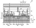
- FIG. 3 is a cross-sectional view schematically showing an example of the device structure of the pixel 10 of the image pickup apparatus 100 according to the first embodiment of the present disclosure.
- Pixels 10 generally include a semiconductor substrate 60, a photoelectric conversion unit 12 arranged above the semiconductor substrate 60, and a conductive structure 89.
- the photoelectric conversion unit 12 is supported by the interlayer insulating layer 90 that covers the semiconductor substrate 60.
- the conductive structure 89 is arranged inside the interlayer insulating layer 90.
- the interlayer insulating layer 90 includes a plurality of insulating layers.
- the conductive structure 89 includes a part of each of a plurality of wiring layers arranged inside the interlayer insulating layer 90.
- the plurality of wiring layers arranged in the interlayer insulating layer 90 include, for example, a wiring layer having an address signal line 34 and a reset signal line 36 as a part thereof, a vertical signal line 35, a power supply wiring 32, a feedback line 53, and the like. It may include a wiring layer having a part thereof. Needless to say, the number of insulating layers and the number of wiring layers in the interlayer insulating layer 90 are not limited to this example and can be set arbitrarily.
- the photoelectric conversion unit 12 includes a pixel electrode 12a formed on the interlayer insulating layer 90, a counter electrode 12c arranged on the incident side of light, and a photoelectric conversion layer arranged between the pixel electrode 12a and the counter electrode 12c. Includes 12b.
- the photoelectric conversion layer 12b is formed of an organic material or an inorganic material such as amorphous silicon, receives light incident through the counter electrode 12c, and generates positive and negative charges by photoelectric conversion.
- the photoelectric conversion layer 12b is typically formed continuously over a plurality of pixels 10.
- the photoelectric conversion layer 12b is formed in a flat plate shape that covers most of the image pickup region R1 of the semiconductor substrate 60 in a plan view. That is, the photoelectric conversion layer 12b is shared by a plurality of pixels 10.
- the photoelectric conversion unit 12 provided for each pixel 10 includes a portion of the photoelectric conversion layer 12b that is different for each pixel 10.
- the photoelectric conversion layer 12b may include a layer made of an organic material and a layer made of an inorganic material. The photoelectric conversion layer 12b may be provided separately for each pixel 10.
- the counter electrode 12c is a translucent electrode formed of a transparent conductive material such as ITO (Indium Tin Oxide).
- transparent as used herein means that the photoelectric conversion layer 12b transmits at least a part of light having a wavelength that can be absorbed, and it is essential that the light is transmitted over the entire wavelength range of visible light. is not.
- the counter electrode 12c is formed continuously over the plurality of pixels 10, similarly to the photoelectric conversion layer 12b. That is, the counter electrode 12c is shared by the plurality of pixels 10.
- the photoelectric conversion unit 12 provided for each pixel 10 includes a portion of the counter electrode 12c that is different for each pixel 10.
- the counter electrode 12c may be provided separately for each pixel 10.
- the counter electrode 12c has a connection with the above-mentioned storage control line 31.
- the potential of the storage control line 31 is controlled to make the potential of the counter electrode 12c higher than the potential of the pixel electrode 12a, so that the positive and negative charges generated by the photoelectric conversion are positive. Charges can be selectively collected by the pixel electrode 12a.
- the counter electrode 12c By forming the counter electrode 12c in the form of a single layer continuous over the plurality of pixels 10, it becomes possible to collectively apply a predetermined potential to the counter electrodes 12c of the plurality of pixels 10.
- the pixel electrode 12a is an electrode formed of a metal such as aluminum or copper, a metal nitride, or polysilicon to which conductivity is imparted by doping with impurities.
- the pixel electrode 12a is electrically separated from the pixel electrode 12a of the other pixel 10 by being spatially separated from the pixel electrode 12a of the other adjacent pixel 10.
- the conductive structure 89 typically includes a plurality of wirings and plugs formed of a metal such as copper or tungsten, or a metal compound such as metal nitride or metal oxide, and a polysilicon plug. One end of the conductive structure 89 is connected to the pixel electrode 12a. By connecting the other end of the conductive structure 89 to the circuit element formed on the semiconductor substrate 60, the pixel electrode 12a of the photoelectric conversion unit 12 and the circuit on the semiconductor substrate 60 are electrically connected to each other.
- the semiconductor substrate 60 includes a support substrate 61 and one or more semiconductor layers formed on the support substrate 61.
- the semiconductor substrate 60 has an n-type semiconductor layer 62n on the support substrate 61 and a p-type semiconductor layer 65p on the n-type semiconductor layer 62n as one or more semiconductor layers.
- the support substrate 61 and the p-type semiconductor layer 65p are electrically connected to each other by a p-type region 64a having a relatively high impurity concentration.
- the semiconductor substrate 60 has a first surface and a second surface opposite to the first surface.
- the first surface is the surface on the side where light is incident.
- the first surface is the surface on the side where the photoelectric conversion unit 12 is provided, among the plurality of surfaces of the semiconductor substrate 60.
- the "front surface” of the semiconductor substrate 60 corresponds to the first surface
- the "back surface” corresponds to the second surface.
- the surface of the semiconductor substrate 60 on the side where the support substrate 61 is provided is the second surface.
- the support substrate 61 contains first conductive type impurities.
- the first conductive type is the p type.
- a p-type silicon substrate is exemplified as the support substrate 61.
- the p-type impurity contained in the support substrate 61 is, for example, boron.
- the support substrate 61 has a connection with a substrate contact provided outside the imaging region R1, which is not shown in FIG. During the operation of the image pickup apparatus 100, the potentials of the support substrate 61 and the p-type semiconductor layer 65p are controlled via the substrate contacts.
- the n-type semiconductor layer 62n is an example of a fourth semiconductor layer of the p-type semiconductor layer 65p, which contains impurities of the second conductive type different from the first conductive type and is located on the opposite side of the photoelectric conversion unit 12. be.
- the n-type semiconductor layer 62n is located between the p-type semiconductor layer 65p and the support substrate 61.
- the second conductive type is n type.
- the n-type impurity contained in the n-type semiconductor layer 62n is, for example, phosphorus.
- a well contact (not shown) is connected to the n-type semiconductor layer 62n.
- the well contact is provided outside the image pickup region R1, and the potential of the n-type semiconductor layer 62n is controlled to be constant via the well contact during the operation of the image pickup apparatus 100. That is, a fixed potential is applied to the n-type semiconductor layer 62n during the operation of the image pickup apparatus 100.
- the n-type semiconductor layer 62n By providing the n-type semiconductor layer 62n, the inflow of minority carriers from the support substrate 61 or the peripheral circuit 40 into the charge storage region 67n where signal charges are stored is suppressed. That is, by providing the n-type semiconductor layer 62n between the support substrate 61 and the p-type semiconductor layer 65p, it is possible to suppress the dark current flowing in the charge storage region 67n.
- the p-type semiconductor layer 65p is an example of a first semiconductor layer containing first conductive type impurities.
- the p-type semiconductor layer 65p is provided on the side closer to the surface of the semiconductor substrate 60 than the n-type semiconductor layer 62n. Specifically, it is provided in contact with the upper surface of the n-type semiconductor layer 62n.
- Each of the n-type semiconductor layer 62n and the p-type semiconductor layer 65p is typically formed by ion implantation of impurities into the semiconductor film formed by epitaxial growth.
- the impurity concentration of the p-type semiconductor layer 65p is higher than the impurity concentration of the support substrate 61.
- the impurity concentration of the support substrate 61 is, for example, about 10 15 cm -3 .
- the impurity concentration of the p-type semiconductor layer 65p can be, for example, about 10 17 cm -3 .
- a plurality of impurity regions are provided in the p-type semiconductor layer 65p of the semiconductor substrate 60.
- the p-type semiconductor layer 65p is provided with a charge storage region 67n, an impurity region 68an, an impurity region 68bn, an impurity region 68cn, an impurity region 68dn, and an impurity region 68en.
- the p-type semiconductor layer 65p is provided with a cutoff structure 69.
- the blocking structure 69 includes an element separation region 69a and an element separation region 69b. Details of the blocking structure 69 will be described later.
- the charge storage region 67n is a second conductive type impurity region in the p-type semiconductor layer 65p, and is an example of a charge storage region for accumulating signal charges.
- the n-type charge storage region 67n is formed in the vicinity of the surface of the semiconductor substrate 60, and at least a part thereof is located on the surface of the semiconductor substrate 60.
- the charge storage region 67n includes a first region 67a and a second region 67b located within the first region 67a and having a higher impurity concentration than the first region 67a.
- the impurity concentration of the first region 67a is, for example, about 10 17 cm -3
- the impurity concentration of the second region 67b is, for example, about 3 ⁇ 10 18 cm -3 .
- "x" means multiplication.
- An insulating layer is arranged on the surface of the semiconductor substrate 60.
- the main surface of the semiconductor substrate 60 on the photoelectric conversion portion 12 side is covered with the first insulating layer 71, the second insulating layer 72, and the third insulating layer 73.
- the first insulating layer 71 is, for example, a thermal oxide film of silicon.
- the second insulating layer 72 is, for example, a silicon dioxide layer, and the third insulating layer 73 is, for example, a silicon nitride layer.
- the second insulating layer 72 may have a laminated structure including a plurality of insulating layers, and similarly, the third insulating layer 73 may also have a laminated structure including a plurality of insulating layers.
- the laminated structure of the first insulating layer 71, the second insulating layer 72 and the third insulating layer 73 has a contact hole h1 on the second region 67b of the charge storage region 67n.
- the contact plug Cp1 which is a part of the conductive structure 89 is connected to the second region 67b via the contact hole h1, whereby the charge storage region 67n is photoelectrically converted via the conductive structure 89. It is electrically connected to the pixel electrode 12a of the unit 12.
- the signal charge generated by the photoelectric conversion unit 12 is stored in the charge storage region 67n.
- junction capacitance formed by the pn junction between the p-type semiconductor layer 65p as the p-well and the n-type charge storage region 67n has a function as a charge storage region that temporarily holds the signal charge. It can be said that the conductive structure 89 and the n-type charge storage region 67n form at least a part of the above-mentioned charge storage node FD.
- the formation of the second region 67b in the charge storage region 67n is not essential. However, by connecting the contact plug Cp1 to the second region 67b having a relatively high impurity concentration, the effect of reducing the contact resistance can be obtained.
- the above-mentioned signal detection circuit 14 is formed on the semiconductor substrate 60.
- the signal detection circuit 14 in the pixel 10 is electrically separated from the signal detection circuit 14 in the other adjacent pixels 10 by arranging the element separation region 69a and the element separation region 69b between the pixels 10 adjacent to each other. Will be done.
- the reset transistor 26 includes an n-type charge storage region 67n as one of the drain region and the source region, and includes an n-type impurity region 68an as the other of the drain region and the source region.
- the reset transistor 26 further includes a gate electrode 26e on the first insulating layer 71, and a portion of the first insulating layer 71 located between the gate electrode 26e and the semiconductor substrate 60 is a gate insulating film of the reset transistor 26. Functions as.
- the impurity region 68an is formed in the p-type semiconductor layer 65p.
- the contact plug Cp2 is connected to the impurity region 68an via the contact hole h2.
- the contact plug Cp2 is electrically connected to the feedback line 53.
- the p-type semiconductor layer 65p is further provided with an n-type impurity region 68bn, an impurity region 68cn, an impurity region 68dn and an impurity region 68en.
- the impurity region 68bn is an example of the first impurity region.
- the impurity concentrations of the impurity region 68an, the impurity region 68bn, the impurity region 68cn, the impurity region 68dn and the impurity region 68en are higher than the impurity concentration of the first region 67a of the charge storage region 67n.
- the signal detection transistor 22 includes an impurity region 68bn, an impurity region 68cn, and a gate electrode 22e on the first insulating layer 71.
- the impurity region 68bn functions as, for example, the drain region of the signal detection transistor 22
- the impurity region 68cn functions as, for example, the source region of the signal detection transistor 22.
- the gate electrode 22e is connected to the portion of the conductive structure 89 that connects the pixel electrode 12a and the contact plug Cp1 to each other in the layer where the address signal line 34 and the reset signal line 36 are located.
- the conductive structure 89 also has an electrical connection with the gate electrode 22e.
- the gate electrode 22e is an example of a first gate that is electrically connected to the photoelectric conversion unit 12.
- a contact plug Cp3 is connected to the impurity region 68bn via the contact hole h3.
- the power supply wiring 32 described above as a source follower power supply is electrically connected to the contact plug Cp3.
- the power supply wiring 32 is not shown in FIG.
- the address transistor 24 is also formed on the semiconductor substrate 60.
- the address transistor 24 includes an impurity region 68en, an impurity region 68dn, and a gate electrode 24e on the first insulating layer 71.
- the n-type impurity region 68en functions as, for example, the drain region of the address transistor 24, and the n-type impurity region 68dn functions as, for example, the source region of the address transistor 24.
- the portion of the first insulating layer 71 located between the gate electrode 24e and the semiconductor substrate 60 functions as the gate insulating film of the address transistor 24.
- the impurity region 68cn and the impurity region 68en are separately provided in the semiconductor substrate 60 and are electrically connected via wiring, but the present invention is not limited to this.
- the impurity region 68cn and the impurity region 68en may be one continuous diffusion region in the semiconductor substrate 60. That is, the signal detection transistor 22 and the address transistor 24 may share one diffusion region. As a result, the signal detection transistor 22 and the address transistor 24 are electrically connected to each other.
- the contact plug Cp4 is connected to the impurity region 68dn via the contact hole h4.
- the contact plug Cp4 is electrically connected to the vertical signal line 35.
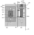
- FIG. 4 is a schematic plan view showing an example of the layout of each element in the pixel 10 of the image pickup apparatus 100 according to the present embodiment.
- the pixel 10 is, for example, a 3 ⁇ m ⁇ 3 ⁇ m square.
- the signal detection transistor 22, the address transistor 24, and the reset transistor 26 are shown so as to appear in one cross section, but this is for convenience of explanation only. Therefore, there may be a portion that does not match between the cross section obtained when the element layout shown in FIG. 4 is cut along a certain line and the cross section shown in FIG.
- the cutoff structure 69 includes an element separation region 69a and an element separation region 69b.
- the element separation region 69a is an example of a second impurity region containing a first conductive type impurity.
- the element separation region 69b is an example of a third impurity region containing a first conductive type impurity.
- the element separation region 69a and the element separation region 69b are formed adjacent to each other in the vicinity of the surface of the semiconductor substrate 60.
- the element separation region 69a and the element separation region 69b are adjacent to each other in a plan view, and at least a part of each is located on the surface of the semiconductor substrate 60.
- the element separation region 69a and the element separation region 69b may not be in contact with each other in a plan view, or may be separated from each other by a predetermined distance.
- the cutoff structure 69 is located between the charge storage region 67n and the signal detection transistor 22. Specifically, in a plan view, at least a part of the cutoff structure 69 is located between the charge storage region 67n and the signal detection transistor 22.
- the element separation region 69a is provided closer to the charge storage region 67n than the element separation region 69b in a plan view. Specifically, the element separation region 69a is provided closer to the reset transistor 26 including the charge storage region 67n as one of the source and the drain than the element separation region 69b.
- A is located between B and C
- B and C means that at least one of a plurality of line segments connecting an arbitrary point in B and an arbitrary point in C is A. Means to pass through.
- A is provided closer to C than B” means that the distance between A and C is shorter than the distance between B and C. That is, in the present embodiment, the distance between the element separation region 69a and the charge storage region 67n is shorter than the distance between the element separation region 69b and the charge storage region 67n.
- the “distance between A and B” means the shortest distance between A and B, that is, the distance between the part of A closest to B and the part of B closest to A.
- an element separation region 69a is arranged around the reset transistor 26.
- An element separation region 69b is arranged around each of the signal detection transistor 22 and the address transistor 24.
- the element separation region 69a and the element separation region 69b are adjacent to each other, and the transistors are electrically separated from each other.
- the element separation region 69a and the element separation region 69b are arranged so as to be separated from the ends of the source and drain of each transistor by about 50 nm.
- the element separation region 69a is not in contact with either the charge storage region 67n or the impurity region 68an.
- the device separation region 69a is formed at a distance of about 50 nm from each of the charge storage region 67n and the impurity region 68an.
- the distance between the element separation region 69a, the charge storage region 67n, and the impurity region 68an may be the same or different from each other.
- the element separation region 69b is not in contact with any of the impurity region 68bn, the impurity region 68cn, the impurity region 68dn, and the impurity region 68en.
- the element separation region 69b is formed, for example, about 50 nm away from each of the impurity region 68bn, the impurity region 68cn, the impurity region 68dn, and the impurity region 68en.
- the intervals between the element separation region 69b and each of the impurity region 68bn, the impurity region 68cn, the impurity region 68dn, and the impurity region 68en may be the same or different from each other.
- the element separation region 69a and the element separation region 69b have different impurity concentrations. Specifically, the impurity concentration in the element separation region 69a is higher than the impurity concentration in the element separation region 69b. Further, the impurity concentration of each of the element separation region 69a and the element separation region 69b is higher than the impurity concentration of the p-type semiconductor layer 65p. For example, the impurity concentration of the element separation region 69b is twice or more or five times or more the impurity concentration of the p-type semiconductor layer 65p. The impurity concentration in the element separation region 69a is 1.2 times or more or 1.5 times or more the impurity concentration in the element separation region 69b.
- the impurity concentration in the element separation region 69a is, for example, about 1.3 ⁇ 10 18 cm -3 .
- the impurity concentration in the element separation region 69b is, for example, about 7 ⁇ 10 17 cm -3 .
- "x" means multiplication.
- the element separation region 69a and the element separation region 69b having different impurity concentrations are arranged between the charge storage region 67n and the impurity region 68bn, respectively.
- the impurity concentration of the element separation region 69a arranged near the reset transistor 26 including the charge storage region 67n as one of the source and drain is higher than the impurity concentration of the element separation region 69b.
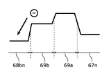
- FIGS. 5A and 5B are diagrams showing the potential of the cutoff structure 69 in the pixel 10 of the image pickup apparatus 100 according to the comparative example and the embodiment, respectively. Specifically, FIGS. 5A and 5B show the potential of the charge storage region 67n, the impurity region 68bn, and the blocking structure 69 disposed between them.
- each of the charge storage region 67n and the impurity region 68bn is not in contact with the blocking structure 69, and a part of the p-type semiconductor layer 65p is present between them.
- a part of the p-type semiconductor layer 65p is not shown.
- a part of the p-type semiconductor layer 65p located between the charge storage region 67n and the cutoff structure 69 is also included.
- a part of the p-type semiconductor layer 65p located between the impurity region 68bn and the blocking structure 69 is included in the vicinity of the boundary between the impurity region 68bn and the blocking structure 69.
- the positional relationship between the element separation region 69a and the element separation region 69b is different between FIGS. 5A and 5B.
- the element separation region 69b having a low impurity concentration is located closer to the charge storage region 67n than the element separation region 69a having a high impurity concentration. This has a positional relationship opposite to that of the embodiment shown in FIG. 5B.
- the impurity region 68bn is the drain of the signal detection transistor 22, and a power supply voltage VDD of about 3.3 V is applied. Therefore, in the vicinity of the boundary between the impurity region 68bn and the cutoff structure 69, impact ionization occurs due to a high electric field, and a small number of carriers are generated in the cutoff structure 69. The majority of the minority carriers flow into the impurity region 68bn depending on the direction of the electric field. However, when the power supply voltage VDD exceeds 3 V and the number of generated minority carriers increases, the minority carriers not only flow into the n-type semiconductor layer 62n arranged on the support substrate 61 side of the pn junction, but also the charge storage region 67n. It was found that it also flows into the dark current and increases the dark current.
- the reason why a small number of carriers flow into the charge storage region 67n will be explained by the potential of each region.
- the impurity concentration in the element separation region 69b near the charge storage region 67n is lower than the impurity concentration in the element separation region 69a, the boundary between the impurity region 68bn and the blocking structure 69.
- the minority carriers generated in the vicinity the minority carriers that were not absorbed by the impurity region 68bn have a potential gradient that easily flows not only with respect to the impurity region 68bn but also with the charge storage region 67n due to the direction of the potential. This also applies, for example, when the impurity concentrations in the element separation region 69a and the element separation region 69b are the same.
- the element separation region 69a when the impurity concentration of the element separation region 69a near the charge storage region 67n is higher than the impurity concentration of the element separation region 69b as in the present embodiment, the element separation region 69a is as shown in FIG. 5B. , Serves as a barrier to the spread of minority carriers. Therefore, it becomes difficult for a small number of carriers to flow in the charge storage region 67n, and dark current can be suppressed.
- the impurity concentration in the element separation region 69b can be lowered, the pn junction electric field in the impurity region 68bn can be reduced and the generation of minority carriers itself can be suppressed. .. As a result, the minority carriers flowing into the charge storage region 67n can be further reduced, so that the dark current can be further suppressed.
- FIG. 6 is a diagram showing the impurity concentration dependence of the cutoff structure 69 of the dark current in the pixels of the image pickup apparatus according to the present embodiment.
- the horizontal axis shows the difference in the impurity concentration of the element separation region 69a with respect to the element separation region 69b, and the higher the numerical value, the higher the impurity concentration in the element separation region 69a.
- the dark current decreases as the impurity concentration in the element separation region 69a becomes higher than that in the element separation region 69b.
- the element separation region 69a and the element separation region 69b are both arranged at a predetermined distance of about 50 nm from the drain region and the source region of the transistor. This is because, for example, when the drain region and the source region and the element separation region 69a having a high impurity concentration are in direct contact with each other, the electric field strength in the depletion region of the pn junction increases and the junction leak increases. This is to prevent the depletion layer of the junction and the element separation region 69a from overlapping.
- the element separation region 69b having a low impurity concentration may be closer to the charge storage region 67n than the element separation region 69a having a high impurity concentration.
- the impurity region of the element separation region 69b is low, the junction leakage due to the pn junction between the element separation region 69b and the charge storage region 67n is suppressed. Therefore, when the junction leak in the charge storage region 67n is dominant over the junction leak in the impurity region 68bn, the device separation region 69b having a low impurity concentration is the charge storage region 67n more than the element separation region 69a having a high impurity concentration. It may be possible to suppress the dark current if it is placed closer to.
- the configuration of the first semiconductor layer is different from that in the first embodiment.
- the first semiconductor layer includes two semiconductor layers having different impurity concentrations.
- the differences from the first embodiment will be mainly described, and the common points will be omitted or simplified.
- FIG. 7 is a cross-sectional view schematically showing an example of the device structure of the pixel 10A of the image pickup apparatus according to the present embodiment.
- FIG. 8 is a schematic plan view showing an example of the layout of each element in the pixel 10A of the image pickup apparatus according to the present embodiment.
- the main difference between the pixel 10A shown in FIG. 7 and the pixel 10 shown in FIG. 3 is that the pixel 10A is provided with a p-type semiconductor layer 65pA instead of the p-type semiconductor layer 65p. ..
- the p-type semiconductor layer 65pA is an example of the first semiconductor layer, and includes a p-type semiconductor layer 65ap and a p-type semiconductor layer 65bp.
- the p-type semiconductor layer 65bp is an example of a second semiconductor layer containing first conductive type impurities.
- the p-type semiconductor layer 65bp is provided around the p-type semiconductor layer 65ap.
- the p-type semiconductor layer 65ap is an example of a third semiconductor layer containing first conductive type impurities.
- the p-type semiconductor layer 65ap includes a charge storage region 67n.
- the p-type semiconductor layer 65ap is adjacent to the p-type semiconductor layer 65bp in a plan view.
- the boundary 65c shown in FIGS. 7 and 8 corresponds to a contact portion between the p-type semiconductor layer 65ap and the p-type semiconductor layer 65bp.
- the boundary 65c overlaps with the element separation region 69a in a plan view. Specifically, the boundary 65c is in contact with the element separation region 69a. That is, the element separation region 69a is in contact with both the p-type semiconductor layer 65ap and the p-type semiconductor layer 65bp.
- the impurity concentration of the p-type semiconductor layer 65ap is different from the impurity concentration of the p-type semiconductor layer 65bp. Specifically, the impurity concentration of the p-type semiconductor layer 65ap is lower than the impurity concentration of the p-type semiconductor layer 65bp. As a result, the impurity concentration in the region surrounding the charge storage region 67n can be lowered, so that the pn junction leak in the charge storage region 67n can be reduced.
- the impurity concentration of the p-type semiconductor layer 65ap is, for example, the same as the impurity concentration of the support substrate 61. Further, the impurity concentration of the p-type semiconductor layer 65bp is lower than the impurity concentration of the device separation region 69b.
- the impurity concentration of the p-type semiconductor layer 65bp may be the same as the impurity concentration of the p-type semiconductor layer 65p according to the first embodiment.
- the impurity concentration of the p-type semiconductor layer 65ap is, for example, about 10 16 cm -3 .
- the impurity concentration of the p-type semiconductor layer 65bp is, for example, about 10 17 cm -3 .
- the element separation region 69a and the charge storage region 67n of the cutoff structure 69 are provided at a predetermined distance such as 50 nm in a plan view.
- the charge storage region 67n is surrounded by the p-type semiconductor layer 65ap having a low impurity concentration and is not in contact with the blocking structure 69 having a high impurity concentration.
- each layer and each region is emphasized in FIG. 7, the distance between the element separation region 69a and the n-type semiconductor layer 62n is based on the distance between the element separation region 69a and the charge storage region 67n. short. Therefore, the minority carriers generated by the junction electric field between the impurity region 68bn and the device separation region 69b form the p-type semiconductor layer 65ap before reaching the charge storage region 67n when viewed from a direction horizontal to the semiconductor substrate 60. It is likely to be discharged to the n-type semiconductor layer 62n via the n-type semiconductor layer 62n. Therefore, the dark current can be further reduced.
- the boundary 65c may overlap with the element separation region 69b in a plan view.
- the boundary 65c may be located between the impurity region 68bn and the device separation region 69b in a plan view. That is, the boundary 65c may not overlap the blocking structure 69 in a plan view, and the blocking structure 69 may be in contact with and surrounded only by the p-type semiconductor layer 65ap.
- the dark current can be reduced by reducing the pn junction leak in the charge storage region 67n and improving the discharge property of the minority carriers.
- the boundary 65c overlaps the impurity region 68bn, the pn junction leak may vary between pixels. Therefore, by providing the boundary 65c so as not to overlap the impurity region 68bn, it is possible to suppress variations in electrical characteristics.
- the cutoff structure 69 has an element separation region 69a and an element separation region 69b having different impurity concentrations, but is not limited thereto.
- the element separation region 69a and the element separation region 69b may have the same impurity concentration.
- FIG. 9 is a cross-sectional view schematically showing an example of the device structure of the pixel 10B of the image pickup apparatus according to the present modification.
- the main difference between the pixel 10B shown in FIG. 9 and the pixel 10A shown in FIG. 7 is that the pixel 10B includes the blocking structure 69B instead of the blocking structure 69.
- the blocking structure 69B is composed of one impurity region having a substantially uniform impurity concentration.
- the impurity concentration of the cutoff structure 69B is higher than the impurity concentration of either the p-type semiconductor layer 65ap or the p-type semiconductor layer 65bp.
- the impurity concentration of the blocking structure 69B may be equal to the impurity concentration of the element separation region 69a according to the first and second embodiments, or may be equal to the impurity concentration of the element separation region 69b.
- the impurity concentration of the cutoff structure 69B may be higher than the impurity concentration of the element separation region 69a and lower than the impurity concentration of the element separation region 69b.
- the impurity concentration of the blocking structure 69B is 7 ⁇ 10 17 cm -3 or more and 1.3 ⁇ 10 18 cm -3 or less, but is not limited thereto.
- the cutoff structure 69B and the charge storage region 67n are provided at a predetermined distance of, for example, 50 nm in a plan view.
- the charge storage region 67n is surrounded by the p-type semiconductor layer 65ap having a low impurity concentration and is not in contact with the blocking structure 69B having a high impurity concentration.
- the boundary 65c overlaps the blocking structure 69B in a plan view. Specifically, the boundary 65c is in contact with the blocking structure 69B. That is, the cutoff structure 69B is in contact with both the p-type semiconductor layer 65ap and the p-type semiconductor layer 65bp.
- the distance between the cutoff structure 69B and the n-type semiconductor layer 62n is shorter than the distance between the cutoff structure 69B and the charge storage region 67n. Therefore, the minority carriers generated in the vicinity of the impurity region 68bn are likely to be discharged to the n-type semiconductor layer 62n via the low-concentration p-type semiconductor layer 65ap. Therefore, as in the first embodiment, the minority carriers flowing in the charge storage region 67n can be suppressed and the dark current can be suppressed as compared with the case where the p-type semiconductor layer 65p has a single structure.
- the boundary 65c may be located between the blocking structure 69B and the impurity region 68bn in a plan view, as in the second embodiment. That is, the boundary 65c may not overlap the blocking structure 69B in a plan view, and the blocking structure 69B may be in contact with and surrounded only by the p-type semiconductor layer 65ap. Even in this case, the dark current can be reduced by reducing the pn junction leak in the charge storage region 67n and improving the discharge property of the minority carriers.
- each of the above-mentioned signal detection transistor 22, address transistor 24, and reset transistor 26 may be an N-channel MOSFET or a P-channel MOSFET.
- the first conductive type impurity is a p-type impurity and the second conductive type impurity is an n-type impurity. It is not necessary that all of these transistors are unified into either N-channel MOSFET or P-channel MOSFET.
- the arrangement of the source and the drain in each of these transistors may be exchanged with each other.
- the present disclosure can be used as an image pickup device capable of suppressing dark current, and can be used, for example, as an image sensor mounted on a camera, a surveillance camera, an in-vehicle camera, or the like.
Landscapes
- Physics & Mathematics (AREA)
- Engineering & Computer Science (AREA)
- Power Engineering (AREA)
- Electromagnetism (AREA)
- Condensed Matter Physics & Semiconductors (AREA)
- General Physics & Mathematics (AREA)
- Computer Hardware Design (AREA)
- Microelectronics & Electronic Packaging (AREA)
- Solid State Image Pick-Up Elements (AREA)
Abstract
This imaging device comprises: a photoelectric converter generating a signal charge via photoelectric conversion; a semiconductor substrate including a first semiconductor layer containing impurities of a first electric conductivity type; a charge accumulation region which is an impurity region of a second electric conductivity type in the first semiconductor layer and accumulates signal charges; a transistor including a first impurity region of the second electric conductivity type in the first semiconductor layer as one of a source or a drain; and a blocking structure positioned between the signal charge accumulation region and the first impurity region. The blocking structure includes a second impurity region of the first electric conductivity type in the first semiconductor layer, and a third impurity region of the first electric conductivity type in the first semiconductor layer, the third impurity region having a different impurity concentration than the second impurity region.
Description
本開示は、撮像装置に関する。
This disclosure relates to an image pickup device.
デジタルカメラなどには、CCD(Charge Coupled Device)イメージセンサおよびCMOS(Complementary Metal Oxide Semiconductor)イメージセンサが広く用いられている。これらのイメージセンサは、半導体基板に形成されたフォトダイオードを有する。
CCD (Charge Coupled Device) image sensors and CMOS (Complementary Metal Oxide Sensor) image sensors are widely used in digital cameras and the like. These image sensors have a photodiode formed on a semiconductor substrate.
例えば、特許文献1に開示されているように、フォトダイオードに代えて、半導体基板の上方に光電変換層を配置した構造も提案されている。このような構造を有する撮像装置は、積層型の撮像装置と呼ばれることがある。積層型の撮像装置では、光電変換によって生成された電荷が、半導体基板に形成された拡散領域などに信号電荷として一時的に蓄積される。蓄積された電荷量に応じた信号が、半導体基板に形成されたCCD回路またはCMOS回路を介して読み出される。
For example, as disclosed in Patent Document 1, a structure in which a photoelectric conversion layer is arranged above a semiconductor substrate is also proposed instead of a photodiode. An image pickup device having such a structure may be referred to as a stacked image pickup device. In the stacked image pickup device, the electric charge generated by the photoelectric conversion is temporarily accumulated as a signal charge in a diffusion region or the like formed on the semiconductor substrate. A signal corresponding to the amount of accumulated charge is read out via a CCD circuit or a CMOS circuit formed on the semiconductor substrate.
画像を表現する信号電荷とは異なる電荷は、信号電荷を一時的に保持する拡散領域へ流入した場合に、得られる画像に劣化を生じさせるノイズの原因となり得る。このような意図しない電荷の移動を抑制できると有益である。以下では、このような、意図しない電荷の移動を、暗電流またはリーク電流と表現することがある。
A charge different from the signal charge that expresses the image can cause noise that causes deterioration of the obtained image when it flows into the diffusion region that temporarily holds the signal charge. It would be beneficial to be able to suppress such unintended charge transfer. In the following, such unintended charge transfer may be referred to as dark current or leak current.
本開示は、暗電流を抑制することができる撮像装置を提供する。
The present disclosure provides an imaging device capable of suppressing dark current.
本開示の一態様に係る撮像装置は、光電変換により信号電荷を生成する光電変換部と、第1導電型の不純物を含む第1半導体層を含む半導体基板と、前記第1半導体層内の第2導電型の不純物領域であって前記信号電荷を蓄積する電荷蓄積領域と、前記第1半導体層内の前記第2導電型の第1不純物領域をソースおよびドレインの一方として含むトランジスタと、前記電荷蓄積領域と前記第1不純物領域との間に位置する遮断構造と、を備える。前記遮断構造は、前記第1半導体層内の前記第1導電型の第2不純物領域と、前記第2不純物領域とは不純物濃度の異なる前記第1半導体層内の前記第1導電型の第3不純物領域と、を含む。
The image pickup apparatus according to one aspect of the present disclosure includes a photoelectric conversion unit that generates a signal charge by photoelectric conversion, a semiconductor substrate including a first semiconductor layer containing a first conductive type impurity, and a first in the first semiconductor layer. A charge storage region that is a two-conducting type impurity region and stores the signal charge, a transistor that includes the second conductive type first impurity region in the first semiconductor layer as one of a source and a drain, and the charge. It is provided with a blocking structure located between the storage region and the first impurity region. The blocking structure is a third of the first conductive type in the first semiconductor layer in which the impurity concentration of the first conductive type second impurity region in the first semiconductor layer is different from that of the second impurity region. Includes impurity regions.
また、包括的または具体的な態様は、素子、デバイス、モジュール、システムまたは方法で実現されてもよい。また、包括的または具体的な態様は、素子、デバイス、装置、モジュール、システムおよび方法の任意の組み合わせによって実現されてもよい。
Further, a comprehensive or specific embodiment may be realized by an element, a device, a module, a system or a method. In addition, the comprehensive or specific embodiment may be realized by any combination of elements, devices, devices, modules, systems and methods.
また、開示された実施の形態の追加的な効果および利点は、明細書および図面から明らかになる。効果および/または利点は、明細書および図面に開示の様々な実施の形態または特徴によって個々に提供され、これらの1つ以上を得るために全てを必要とはしない。
Also, the additional effects and advantages of the disclosed embodiments will be apparent from the specification and drawings. The effects and / or advantages are provided individually by the various embodiments or features disclosed in the specification and drawings, and not all are required to obtain one or more of these.
本開示によれば、暗電流を抑制することができる。
According to the present disclosure, dark current can be suppressed.
(本開示の概要)
本開示の一態様の概要は以下のとおりである。 (Summary of this disclosure)
The outline of one aspect of the present disclosure is as follows.
本開示の一態様の概要は以下のとおりである。 (Summary of this disclosure)
The outline of one aspect of the present disclosure is as follows.
本開示の一態様に係る撮像装置は、光電変換により信号電荷を生成する光電変換部と、第1導電型の不純物を含む第1半導体層を含む半導体基板と、前記第1半導体層内の第2導電型の不純物領域であって前記信号電荷を蓄積する電荷蓄積領域と、前記第1半導体層内の前記第2導電型の第1不純物領域をソースおよびドレインの一方として含むトランジスタと、前記電荷蓄積領域と前記第1不純物領域との間に位置する遮断構造と、を備える。前記遮断構造は、前記第1半導体層内の前記第1導電型の第2不純物領域と、前記第2不純物領域とは不純物濃度の異なる前記第1半導体層内の前記第1導電型の第3不純物領域と、を含む。
The image pickup apparatus according to one aspect of the present disclosure includes a photoelectric conversion unit that generates a signal charge by photoelectric conversion, a semiconductor substrate including a first semiconductor layer containing a first conductive type impurity, and a first in the first semiconductor layer. A charge storage region that is a two-conducting type impurity region and stores the signal charge, a transistor that includes the second conductive type first impurity region in the first semiconductor layer as one of a source and a drain, and the charge. It is provided with a blocking structure located between the storage region and the first impurity region. The blocking structure is a third of the first conductive type in the first semiconductor layer in which the impurity concentration of the first conductive type second impurity region in the first semiconductor layer is different from that of the second impurity region. Includes impurity regions.
このように、遮断構造が、第2導電型の第1不純物領域と電荷蓄積領域との間に、第1導電型の不純物濃度の高い領域を含むことで、第2導電型の第1不純物領域のpn接合で発生した少数キャリアの再結合を加速させ、電荷蓄積領域への少数キャリアの流入を抑制することができる。このため、遮断構造が設けられることで、電荷蓄積領域に流れる暗電流を抑制することができる。
As described above, the blocking structure includes a region having a high impurity concentration of the first conductive type between the first impurity region of the second conductive type and the charge storage region, so that the first impurity region of the second conductive type is included. It is possible to accelerate the recombination of minority carriers generated in the pn junction and suppress the inflow of minority carriers into the charge storage region. Therefore, by providing the cutoff structure, it is possible to suppress the dark current flowing in the charge storage region.
一方で、第1導電型の遮断構造中で再結合されなかった少数キャリアは、不純物濃度が低くなる方向に拡散する特性を有する。このため、第1不純物領域だけではなく、電荷蓄積領域にも流入する可能性がある。
On the other hand, the minority carriers that were not recombined in the first conductive type blocking structure have the property of diffusing in the direction of lowering the impurity concentration. Therefore, it may flow into not only the first impurity region but also the charge storage region.
これに対して、本開示の一態様に係る撮像装置によれば、平面視において、前記第2不純物領域と前記電荷蓄積領域との距離は、前記第3不純物領域と前記電荷蓄積領域との距離より短くてもよい。また、例えば、前記第2不純物領域の不純物濃度は、前記第3不純物領域の不純物濃度よりも高くてもよい。
On the other hand, according to the image pickup apparatus according to one aspect of the present disclosure, the distance between the second impurity region and the charge storage region is the distance between the third impurity region and the charge storage region in a plan view. It may be shorter. Further, for example, the impurity concentration in the second impurity region may be higher than the impurity concentration in the third impurity region.
これにより、第2不純物領域は、第1不純物領域のpn接合で発生した少数キャリアに対する拡散バリアとして機能する。このため、電荷蓄積領域への少数キャリアの流入を抑制することができる。したがって、電荷蓄積領域に発生する暗電流に起因する画像の劣化を更に抑制することができる。
Thereby, the second impurity region functions as a diffusion barrier for the minority carriers generated by the pn junction of the first impurity region. Therefore, it is possible to suppress the inflow of minority carriers into the charge storage region. Therefore, deterioration of the image due to the dark current generated in the charge storage region can be further suppressed.
また、例えば、前記第2不純物領域は、前記第3不純物領域と直接接していてもよい。
Further, for example, the second impurity region may be in direct contact with the third impurity region.
また、例えば、前記第1半導体層は、前記第1導電型の不純物を含む第2半導体層と、平面視において、前記第2半導体層に隣接し、前記第2半導体層とは不純物濃度の異なる第3半導体層と、を含んでいてもよい。前記電荷蓄積領域は、前記第3半導体層内に含まれていてもよい。前記第1不純物領域は、前記第2半導体層内に含まれていてもよい。前記第2不純物領域は、平面視において、前記第2半導体層と前記第3半導体層との境界に重なっていてもよい。
Further, for example, the first semiconductor layer is adjacent to the second semiconductor layer containing the first conductive type impurities and the second semiconductor layer in a plan view, and the impurity concentration is different from that of the second semiconductor layer. It may include a third semiconductor layer. The charge storage region may be included in the third semiconductor layer. The first impurity region may be contained in the second semiconductor layer. The second impurity region may overlap the boundary between the second semiconductor layer and the third semiconductor layer in a plan view.
これによれば、電荷蓄積領域を取り囲む領域の不純物濃度を低くすることができるため、電荷蓄積領域のpn接合リークを低減できる。
According to this, since the impurity concentration in the region surrounding the charge storage region can be lowered, the pn junction leak in the charge storage region can be reduced.
また、例えば、前記半導体基板は、さらに、前記第2導電型の不純物を含む第4半導体層を含んでもよく、前記第1半導体層は、前記光電変換部と前記第4半導体層との間に位置していてもよい。
Further, for example, the semiconductor substrate may further include a fourth semiconductor layer containing the second conductive type impurities, and the first semiconductor layer is placed between the photoelectric conversion unit and the fourth semiconductor layer. It may be located.
これにより、第1不純物領域のpn接合で発生した少数キャリアは、不純物濃度が低い第3半導体層を通じて第4半導体層に排出されやすくなる。このため、電荷蓄積領域への少数キャリアの流入を抑制することができ、暗電流を更に抑制することができる。
As a result, the minority carriers generated at the pn junction of the first impurity region are likely to be discharged to the fourth semiconductor layer through the third semiconductor layer having a low impurity concentration. Therefore, the inflow of a small number of carriers into the charge storage region can be suppressed, and the dark current can be further suppressed.
また、例えば、前記第3半導体層の不純物濃度は、前記第2半導体層の不純物濃度より低くてもよい。
Further, for example, the impurity concentration of the third semiconductor layer may be lower than the impurity concentration of the second semiconductor layer.
これにより、第3半導体層の不純物濃度が低くなることにより、第3半導体層内の電荷蓄積領域のpn接合リークを低減することができる。よって、暗電流を更に抑制することができる。
As a result, the impurity concentration of the third semiconductor layer is lowered, so that the pn junction leak in the charge storage region in the third semiconductor layer can be reduced. Therefore, the dark current can be further suppressed.
また、例えば、前記第2不純物領域の少なくとも一部、前記第3不純物領域の少なくとも一部、または前記第2不純物領域の前記少なくとも一部及び前記第3不純物領域の前記少なくとも一部の両方は、前記半導体基板の表面に位置していてもよい。
Further, for example, at least a part of the second impurity region, at least a part of the third impurity region, or at least a part of the second impurity region and at least a part of the third impurity region may be present. It may be located on the surface of the semiconductor substrate.
また、例えば、前記トランジスタは、前記光電変換部と電気的に接続する第1ゲートを含んでいてもよい。
Further, for example, the transistor may include a first gate that is electrically connected to the photoelectric conversion unit.
また、例えば、平面視において、前記第2不純物領域は、前記電荷蓄積領域を取り囲んでもよい。
Further, for example, in a plan view, the second impurity region may surround the charge storage region.
また、例えば、平面視において、前記第3不純物領域は、前記トランジスタを取り囲んでもよい。
Further, for example, in a plan view, the third impurity region may surround the transistor.
また、例えば、平面視において、前記第2不純物領域は、前記第3不純物領域と重ならなくてもよい。
Further, for example, in a plan view, the second impurity region does not have to overlap with the third impurity region.
本開示において、回路、ユニット、装置、部材もしくは部の全部または一部、またはブロック図の機能ブロックの全部もしくは一部は、半導体装置、半導体集積回路(IC)、またはLSI(large scale integration)を含む一つまたは複数の電子回路によって実行されてもよい。LSIまたはICは、一つのチップに集積されてもよいし、複数のチップを組み合わせて構成されてもよい。例えば、記憶素子以外の機能ブロックは、一つのチップに集積されてもよい。ここでは、LSIまたはICと呼んでいるが、集積の度合いによって呼び方が変わり、システムLSI、VLSI(Very Large Scale Integration)、もしくはULSI(Ultra Large Scale Integration)と呼ばれるものであってもよい。LSIの製造後にプログラムされる、Field Programmable Gate Array(FPGA)、またはLSI内部の接合関係の再構成またはLSI内部の回路区画のセットアップができるReconfigurable Logic Deviceも同じ目的で使うことができる。
In the present disclosure, all or part of a circuit, unit, device, member or part, or all or part of a functional block in a block diagram is a semiconductor device, a semiconductor integrated circuit (IC), or an LSI (lage scale integration). It may be performed by one or more electronic circuits including. The LSI or IC may be integrated on one chip, or may be configured by combining a plurality of chips. For example, functional blocks other than the storage element may be integrated on one chip. Here, it is called LSI or IC, but the name changes depending on the degree of integration, and it may be called system LSI, VLSI (Very Large Scale Integration), or ULSI (Ultra Large Scale Integration). Field Programmable Gate Array (FPGA), which is programmed after the LSI is manufactured, or Reconfigurable Logic Device, which can reconfigure the connection relationship inside the LSI or set up the circuit partition inside the LSI, can also be used for the same purpose.
さらに、回路、ユニット、装置、部材もしくは部の全部または一部の機能または操作は、ソフトウェア処理によって実行することが可能である。この場合、ソフトウェアは一つまたは複数のROM、光学ディスク、ハードディスクドライブなどの非一時的記録媒体に記録され、ソフトウェアが処理装置(processor)によって実行されたときに、そのソフトウェアで特定された機能が処理装置(processor)および周辺装置によって実行される。システムまたは装置は、ソフトウェアが記録されている一つまたは複数の非一時的記録媒体、処理装置(processor)、および必要とされるハードウェアデバイス、例えばインターフェースを備えていてもよい。
Furthermore, all or part of the functions or operations of circuits, units, devices, members or parts can be performed by software processing. In this case, the software is recorded on a non-temporary recording medium such as one or more ROMs, optical disks, hard disk drives, etc., and when the software is executed by a processor, the functions identified by the software It is executed by a processor and peripheral devices. The system or device may include one or more non-temporary recording media on which the software is recorded, a processor, and the required hardware device, such as an interface.
以下、図面を参照しながら、本開示の実施の形態を詳細に説明する。なお、以下で説明する実施の形態は、いずれも包括的または具体的な例を示す。以下の実施の形態で示される数値、形状、材料、構成要素、構成要素の配置および接続形態、ステップ、ステップの順序などは、一例であり、本開示を限定する主旨ではない。本明細書において説明される種々の態様は、矛盾が生じない限り互いに組み合わせることが可能である。また、以下の実施の形態における構成要素のうち、独立請求項に記載されていない構成要素については、任意の構成要素として説明される。以下の説明において、実質的に同じ機能を有する構成要素は共通の参照符号で示し、説明を省略することがある。また、図面が過度に複雑になることを避けるために、一部の要素の図示を省略することがある。
Hereinafter, embodiments of the present disclosure will be described in detail with reference to the drawings. In addition, all of the embodiments described below show comprehensive or specific examples. The numerical values, shapes, materials, components, arrangement and connection forms of the components, steps, the order of steps, etc. shown in the following embodiments are examples, and are not intended to limit the present disclosure. The various aspects described herein can be combined with each other as long as there is no conflict. Further, among the components in the following embodiments, the components not described in the independent claims are described as arbitrary components. In the following description, components having substantially the same function are indicated by common reference numerals, and the description may be omitted. In addition, some elements may be omitted in order to prevent the drawings from becoming excessively complicated.
また、図面に示す各種の要素は、本開示の理解のために模式的に示したにすぎず、寸法比および外観などは実物と異なり得る。つまり、各図は、模式図であり、必ずしも厳密に図示されたものではない。したがって、例えば、各図において縮尺などは必ずしも一致しない。
Further, the various elements shown in the drawings are merely schematically shown for the purpose of understanding the present disclosure, and the dimensional ratio, appearance, etc. may differ from the actual ones. That is, each figure is a schematic view and is not necessarily exactly illustrated. Therefore, for example, the scales and the like do not always match in each figure.
また、本明細書において、平行または均一などの要素間の関係性を示す用語、および、円形または矩形などの要素の形状を示す用語、ならびに、数値範囲は、厳格な意味のみを表す表現ではなく、実質的に同等な範囲、例えば数%程度の差異をも含むことを意味する表現である。
Further, in the present specification, terms indicating relationships between elements such as parallel or uniform, terms indicating the shape of elements such as circles or rectangles, and numerical ranges are not expressions that express only strict meanings. , Is an expression meaning that a substantially equivalent range, for example, a difference of about several percent is included.
また、本明細書において、「上方」および「下方」という用語は、絶対的な空間認識における上方向(鉛直上方)および下方向(鉛直下方)を指すものではなく、積層構成における積層順を基に相対的な位置関係により規定される用語として用いる。具体的には、撮像装置の受光側を「上方」とし、受光側と反対側を「下方」とする。各部材の「上面」、「下面」についても同様に、撮像装置の受光側に対向する面を「上面」とし、受光側と反対側に対向する面を「下面」とする。なお、「上方」、「下方」、「上面」および「下面」などの用語は、あくまでも部材間の相互の配置を指定するために用いており、撮像装置の使用時における姿勢を限定する意図ではない。また、「上方」および「下方」という用語は、2つの構成要素が互いに間隔を空けて配置されて2つの構成要素の間に別の構成要素が存在する場合のみならず、2つの構成要素が互いに密着して配置されて2つの構成要素が接する場合にも適用される。また、本明細書において、「平面視」とは、半導体基板に垂直な方向から見たときのことを言う。
Further, in the present specification, the terms "upper" and "lower" do not refer to the upward direction (vertically upward) and the downward direction (vertically downward) in absolute spatial recognition, but are based on the stacking order in the laminated configuration. It is used as a term defined by the relative positional relationship. Specifically, the light receiving side of the image pickup device is referred to as "upper", and the side opposite to the light receiving side is referred to as "lower". Similarly, for the "upper surface" and "lower surface" of each member, the surface facing the light receiving side of the image pickup apparatus is referred to as the "upper surface", and the surface facing the light receiving side is referred to as the "lower surface". The terms "upper", "lower", "upper surface" and "lower surface" are used only to specify the mutual arrangement between the members, and are intended to limit the posture when the image pickup device is used. do not have. Also, the terms "upper" and "lower" are used not only when the two components are spaced apart from each other and another component exists between the two components, but also when the two components are present. It also applies when the two components are placed in close contact with each other and touch each other. Further, in the present specification, "planar view" means a view from a direction perpendicular to the semiconductor substrate.
(実施の形態1)
図1は、本開示の実施の形態1に係る撮像装置の例示的な構成を示す図である。図1に示す撮像装置100は、半導体基板60に形成された複数の画素10および周辺回路40を有する。 (Embodiment 1)
FIG. 1 is a diagram showing an exemplary configuration of an image pickup apparatus according to a first embodiment of the present disclosure. Theimage pickup apparatus 100 shown in FIG. 1 has a plurality of pixels 10 and peripheral circuits 40 formed on the semiconductor substrate 60.
図1は、本開示の実施の形態1に係る撮像装置の例示的な構成を示す図である。図1に示す撮像装置100は、半導体基板60に形成された複数の画素10および周辺回路40を有する。 (Embodiment 1)
FIG. 1 is a diagram showing an exemplary configuration of an image pickup apparatus according to a first embodiment of the present disclosure. The
各画素10は、光電変換部12を含む。光電変換部12は、光の入射を受けて正および負の電荷、典型的には、正孔-電子対を発生させる。光電変換部12は、半導体基板60の上方に配置された光電変換層を含む光電変換構造、あるいは、半導体基板60に形成されたフォトダイオードであり得る。なお、図1では、各画素10の光電変換部12が空間的に互いに分離されているように図示されているが、これは説明の便宜に過ぎず、複数の画素10の光電変換部12が互いに間隔をあけずに半導体基板60上に連続的に配置されることもあり得る。
Each pixel 10 includes a photoelectric conversion unit 12. The photoelectric conversion unit 12 receives the incident light to generate positive and negative charges, typically hole-electron pairs. The photoelectric conversion unit 12 may be a photoelectric conversion structure including a photoelectric conversion layer arranged above the semiconductor substrate 60, or a photodiode formed on the semiconductor substrate 60. In FIG. 1, the photoelectric conversion unit 12 of each pixel 10 is shown so as to be spatially separated from each other, but this is only for convenience of explanation, and the photoelectric conversion unit 12 of the plurality of pixels 10 is shown. It may be continuously arranged on the semiconductor substrate 60 without being spaced from each other.
図1に示す例では、画素10が、m行n列の複数の行および列に配列されている。ここで、m、nは、独立して1以上の整数を表す。画素10は、半導体基板60に例えば2次元に配列されることにより、撮像領域R1を形成する。各画素10が、例えば半導体基板60の上方に配置された光電変換部12を有する場合、撮像領域R1は、半導体基板60のうち、光電変換部12によって覆われている領域として規定され得る。
In the example shown in FIG. 1, the pixels 10 are arranged in a plurality of rows and columns of m rows and n columns. Here, m and n independently represent integers of 1 or more. The pixels 10 are arranged on the semiconductor substrate 60, for example, in two dimensions to form an imaging region R1. When each pixel 10 has, for example, a photoelectric conversion unit 12 arranged above the semiconductor substrate 60, the imaging region R1 may be defined as a region of the semiconductor substrate 60 covered by the photoelectric conversion unit 12.
画素10の数および配置は、図示する例に限定されない。例えば、撮像装置100に含まれる画素10の数は、1つであってもよい。この例では、各画素10の中心が正方格子の格子点上に位置しているが、例えば、各画素10の中心が、三角格子、六角格子などの格子点上に位置するように複数の画素10を配置してもよい。例えば、画素10を1次元に配列してもよく、この場合、撮像装置100をラインセンサとして利用し得る。
The number and arrangement of the pixels 10 are not limited to the illustrated example. For example, the number of pixels 10 included in the image pickup apparatus 100 may be one. In this example, the center of each pixel 10 is located on a grid point of a square grid, but for example, a plurality of pixels so that the center of each pixel 10 is located on a grid point such as a triangular grid or a hexagonal grid. 10 may be arranged. For example, the pixels 10 may be arranged one-dimensionally, and in this case, the image pickup apparatus 100 may be used as a line sensor.
図1に例示する構成において、周辺回路40は、垂直走査回路42、および水平信号読み出し回路44を含む。図1に例示するように、周辺回路40は、付加的に、制御回路46を含み得る。また、周辺回路40が、例えば、画素10などに対して所定の電圧を供給する電圧供給回路をさらに含むこともあり得る。周辺回路40は、信号処理回路、出力回路などをさらに含んでいてもかまわない。周辺回路40は、周辺領域R2に配置されている。周辺領域R2は、撮像領域R1の周囲の領域である。
In the configuration exemplified in FIG. 1, the peripheral circuit 40 includes a vertical scanning circuit 42 and a horizontal signal readout circuit 44. As illustrated in FIG. 1, the peripheral circuit 40 may additionally include a control circuit 46. Further, the peripheral circuit 40 may further include a voltage supply circuit that supplies a predetermined voltage to, for example, the pixel 10. The peripheral circuit 40 may further include a signal processing circuit, an output circuit, and the like. The peripheral circuit 40 is arranged in the peripheral region R2. The peripheral region R2 is a region around the imaging region R1.
垂直走査回路42は、行走査回路とも呼ばれ、複数の画素10の各行に対応して設けられたアドレス信号線34との接続を有する。後述するように、複数の画素10の各行に対応して設けられる信号線は、アドレス信号線34に限定されず、垂直走査回路42には、複数の画素10の行ごとに複数の種類の信号線が接続され得る。水平信号読み出し回路44は、列走査回路とも呼ばれ、複数の画素10の各列に対応して設けられた垂直信号線35との接続を有する。
The vertical scanning circuit 42, also called a row scanning circuit, has a connection with an address signal line 34 provided corresponding to each row of the plurality of pixels 10. As will be described later, the signal line provided corresponding to each line of the plurality of pixels 10 is not limited to the address signal line 34, and the vertical scanning circuit 42 has a plurality of types of signals for each line of the plurality of pixels 10. Wires can be connected. The horizontal signal readout circuit 44, also referred to as a row scanning circuit, has a connection with a vertical signal line 35 provided corresponding to each row of the plurality of pixels 10.
制御回路46は、撮像装置100の例えば外部から与えられる指令データ、クロックなどを受け取って撮像装置100の全体を制御する。典型的には、制御回路46は、タイミングジェネレータを有し、垂直走査回路42、水平信号読み出し回路44、電圧供給回路などに駆動信号を供給する。図1中、制御回路46から延びる矢印は、制御回路46からの出力信号の流れを模式的に表現している。制御回路46は、例えば1以上のプロセッサを含むマイクロコントローラによって実現され得る。制御回路46の機能は、汎用の処理回路とソフトウェアとの組み合わせによって実現されてもよいし、このような処理に特化したハードウェアによって実現されてもよい。
The control circuit 46 receives command data, a clock, or the like given from the outside of the image pickup device 100, and controls the entire image pickup device 100. Typically, the control circuit 46 has a timing generator and supplies a drive signal to a vertical scanning circuit 42, a horizontal signal readout circuit 44, a voltage supply circuit, and the like. In FIG. 1, the arrow extending from the control circuit 46 schematically represents the flow of the output signal from the control circuit 46. The control circuit 46 may be implemented, for example, by a microcontroller including one or more processors. The function of the control circuit 46 may be realized by a combination of a general-purpose processing circuit and software, or may be realized by hardware specialized for such processing.
図2は、本開示の実施の形態1に係る撮像装置の例示的な回路構成を模式的に示す模式図である。図2では、図面が複雑となることを避けるために、2行2列に配列された4つの画素10が代表して示されている。これらの画素10の各々は、図1に示す画素10の一例である。画素10の各々は、光電変換部12を有し、光電変換部12に電気的に接続された信号検出回路14を含む。後に図3を参照して詳しく説明するように、光電変換部12は、半導体基板60の上方に配置された光電変換層12bを含む。すなわち、ここでは、撮像装置100として積層型の撮像装置を例示する。
FIG. 2 is a schematic diagram schematically showing an exemplary circuit configuration of the image pickup apparatus according to the first embodiment of the present disclosure. In FIG. 2, four pixels 10 arranged in two rows and two columns are represented as representatives in order to avoid complication of the drawing. Each of these pixels 10 is an example of the pixel 10 shown in FIG. Each of the pixels 10 has a photoelectric conversion unit 12, and includes a signal detection circuit 14 electrically connected to the photoelectric conversion unit 12. As will be described in detail later with reference to FIG. 3, the photoelectric conversion unit 12 includes a photoelectric conversion layer 12b arranged above the semiconductor substrate 60. That is, here, a stacked image pickup device is exemplified as the image pickup device 100.
各画素10の光電変換部12は、蓄積制御線31との接続を有する。撮像装置100の動作時、蓄積制御線31には所定の電圧が印加される。例えば、光電変換によって生成された正および負の電荷のうち、正の電荷を信号電荷として利用する場合であれば、撮像装置100の動作時に蓄積制御線31に例えば10V程度の正電圧が印加され得る。以下では、信号電荷として正孔を利用する場合を例示する。
The photoelectric conversion unit 12 of each pixel 10 has a connection with the storage control line 31. During the operation of the image pickup apparatus 100, a predetermined voltage is applied to the storage control line 31. For example, in the case of using the positive charge as the signal charge among the positive and negative charges generated by the photoelectric conversion, a positive voltage of, for example, about 10 V is applied to the storage control line 31 during the operation of the image pickup apparatus 100. obtain. In the following, a case where holes are used as signal charges will be illustrated.
図2に例示する構成において、信号検出回路14は、信号検出トランジスタ22、アドレストランジスタ24およびリセットトランジスタ26を含む。後に図面を参照して詳しく説明するように、信号検出トランジスタ22、アドレストランジスタ24およびリセットトランジスタ26は、典型的には、光電変換部12を支持する半導体基板60に形成された電界効果トランジスタ(FET:Field Effect Transistor)である。以下では、特に断りの無い限り、トランジスタとしてNチャネルMOSFETを用いる例を説明する。
In the configuration exemplified in FIG. 2, the signal detection circuit 14 includes a signal detection transistor 22, an address transistor 24, and a reset transistor 26. As will be described in detail later with reference to the drawings, the signal detection transistor 22, the address transistor 24 and the reset transistor 26 are typically field effect transistors (FETs) formed on the semiconductor substrate 60 supporting the photoelectric conversion unit 12. : Field Effect Transistor). In the following, an example of using an N-channel MOSFET as a transistor will be described unless otherwise specified.
図2において模式的に示すように、信号検出トランジスタ22のゲートは、光電変換部12に電気的に接続されている。図示する例において、信号検出トランジスタ22のゲートを光電変換部12に接続する電荷蓄積ノードFDは、光電変換部12によって生成された電荷を一時的に保持する機能を有する。動作時に蓄積制御線31に所定の電圧を印加することにより、電荷蓄積ノードFDに例えば正孔を信号電荷として蓄積することができる。後に図面を参照して説明するように、電荷蓄積ノードFDは、半導体基板60に形成された不純物領域をその一部に含む。
As schematically shown in FIG. 2, the gate of the signal detection transistor 22 is electrically connected to the photoelectric conversion unit 12. In the illustrated example, the charge storage node FD connecting the gate of the signal detection transistor 22 to the photoelectric conversion unit 12 has a function of temporarily holding the charge generated by the photoelectric conversion unit 12. By applying a predetermined voltage to the storage control line 31 during operation, for example, holes can be stored as signal charges in the charge storage node FD. As will be described later with reference to the drawings, the charge storage node FD includes an impurity region formed on the semiconductor substrate 60 as a part thereof.
信号検出トランジスタ22のドレインは、撮像装置100の動作時に各画素10に例えば3.3V程度の電源電圧VDDを供給する電源配線32に接続され、ソースは、アドレストランジスタ24を介して垂直信号線35に接続される。信号検出トランジスタ22は、ドレインに電源電圧VDDの供給を受けることにより、電荷蓄積ノードFDに蓄積された信号電荷の量に応じた信号電圧を出力する。
The drain of the signal detection transistor 22 is connected to a power supply wiring 32 that supplies a power supply voltage VDD of, for example, about 3.3 V to each pixel 10 when the image pickup apparatus 100 is operated, and the source is a vertical signal line 35 via the address transistor 24. Connected to. By receiving the power supply voltage VDD from the drain, the signal detection transistor 22 outputs a signal voltage corresponding to the amount of signal charge stored in the charge storage node FD.
信号検出トランジスタ22と垂直信号線35との間に接続されたアドレストランジスタ24のゲートには、アドレス信号線34が接続されている。垂直走査回路42は、アドレストランジスタ24のオンおよびオフを制御する行選択信号をアドレス信号線34に印加する。このことにより、選択した画素10の信号検出トランジスタ22の出力を、対応する垂直信号線35に読み出すことができる。なお、アドレストランジスタ24の配置は、図2に示す例に限定されず、信号検出トランジスタ22のドレインと電源配線32との間であってもよい。
The address signal line 34 is connected to the gate of the address transistor 24 connected between the signal detection transistor 22 and the vertical signal line 35. The vertical scanning circuit 42 applies a row selection signal that controls turning on and off of the address transistor 24 to the address signal line 34. As a result, the output of the signal detection transistor 22 of the selected pixel 10 can be read out to the corresponding vertical signal line 35. The arrangement of the address transistor 24 is not limited to the example shown in FIG. 2, and may be between the drain of the signal detection transistor 22 and the power supply wiring 32.
垂直信号線35の各々には、負荷回路45およびカラム信号処理回路47が接続されている。負荷回路45は、信号検出トランジスタ22とともにソースフォロワ回路を形成する。カラム信号処理回路47は、行信号蓄積回路とも呼ばれ、相関二重サンプリングに代表される雑音抑圧信号処理およびアナログ-デジタル変換などを行う。水平信号読み出し回路44は、複数のカラム信号処理回路47から水平共通信号線49に信号を順次読み出す。負荷回路45およびカラム信号処理回路47は、上述の周辺回路40の一部であり得る。
A load circuit 45 and a column signal processing circuit 47 are connected to each of the vertical signal lines 35. The load circuit 45 forms a source follower circuit together with the signal detection transistor 22. The column signal processing circuit 47, also called a row signal storage circuit, performs noise suppression signal processing represented by correlated double sampling, analog-to-digital conversion, and the like. The horizontal signal reading circuit 44 sequentially reads signals from the plurality of column signal processing circuits 47 to the horizontal common signal line 49. The load circuit 45 and the column signal processing circuit 47 may be part of the peripheral circuit 40 described above.
リセットトランジスタ26のゲートには、垂直走査回路42との接続を有するリセット信号線36が接続される。リセット信号線36は、アドレス信号線34と同様に複数の画素10の行ごとに設けられる。垂直走査回路42は、アドレス信号線34に行選択信号を印加することにより、リセットの対象となる画素10を行単位で選択することができ、リセット信号線36を介してリセット信号をリセットトランジスタ26のゲートに印加することにより、選択された行のリセットトランジスタ26のオンおよびオフを切り替えることができる。リセットトランジスタ26がオンとされることにより、電荷蓄積ノードFDの電位がリセットされる。
A reset signal line 36 having a connection with the vertical scanning circuit 42 is connected to the gate of the reset transistor 26. The reset signal line 36 is provided for each line of the plurality of pixels 10 in the same manner as the address signal line 34. The vertical scanning circuit 42 can select the pixel 10 to be reset in line units by applying a row selection signal to the address signal line 34, and resets the reset signal via the reset signal line 36. By applying to the gate of, the reset transistor 26 of the selected row can be switched on and off. When the reset transistor 26 is turned on, the potential of the charge storage node FD is reset.
この例では、リセットトランジスタ26のドレインおよびソースの一方は、電荷蓄積ノードFDに接続され、ドレインおよびソースの他方は、複数の画素10の列ごとに設けられたフィードバック線53のうちの対応する1つに接続されている。すなわち、この例では、光電変換部12の電荷を初期化するリセット電圧として、フィードバック線53の電圧が電荷蓄積ノードFDに供給される。
In this example, one of the drain and source of the reset transistor 26 is connected to the charge storage node FD, and the other of the drain and source is the corresponding one of the feedback lines 53 provided for each row of the plurality of pixels 10. It is connected to one. That is, in this example, the voltage of the feedback line 53 is supplied to the charge storage node FD as the reset voltage for initializing the charge of the photoelectric conversion unit 12.
図2に例示する構成において、撮像装置100は、反転増幅器50を帰還経路の一部に含むフィードバック回路16を有する。図2に示すように、反転増幅器50は、複数の画素10の列ごとに設けられ、上述のフィードバック線53は、複数の反転増幅器50のうちの対応する1つの出力端子に接続される。反転増幅器50は、上述の周辺回路40の一部であり得る。
In the configuration exemplified in FIG. 2, the image pickup apparatus 100 has a feedback circuit 16 including an inverting amplifier 50 as a part of the feedback path. As shown in FIG. 2, the inverting amplifier 50 is provided for each row of the plurality of pixels 10, and the feedback line 53 described above is connected to the corresponding output terminal of the plurality of inverting amplifiers 50. The inverting amplifier 50 may be part of the peripheral circuit 40 described above.
図示するように、反転増幅器50の反転入力端子は、対応する列の垂直信号線35に接続され、反転増幅器50の非反転入力端子には、撮像装置100の動作時、例えば1Vまたは1V近傍の正電圧である参照電圧Vrefが供給される。アドレストランジスタ24およびリセットトランジスタ26をオンとすることにより、その画素10の出力を負帰還させる帰還経路を形成することができ、帰還経路の形成により、垂直信号線35の電圧が、反転増幅器50の非反転入力端子への入力電圧Vrefに収束する。換言すれば、帰還経路の形成により、電荷蓄積ノードFDの電圧が、垂直信号線35の電圧がVrefとなるような電圧にリセットされる。電圧Vrefとしては、電源電圧および接地の範囲内の任意の大きさの電圧を用い得る。帰還経路の形成により、リセットトランジスタ26のオフに伴って発生するリセットノイズを低減可能である。フィードバックを利用したリセットノイズの抑制の詳細は、特許文献1において説明されている。参考のために、特許文献1の開示内容の全てを本明細書に援用する。
As shown, the inverting input terminal of the inverting amplifier 50 is connected to the vertical signal line 35 of the corresponding column, and the non-inverting input terminal of the inverting amplifier 50 is connected to the non-inverting input terminal of the inverting amplifier 50 during operation of the image pickup apparatus 100, for example, near 1V or 1V. A reference voltage Vref, which is a positive voltage, is supplied. By turning on the address transistor 24 and the reset transistor 26, a feedback path for negatively feeding back the output of the pixel 10 can be formed, and by forming the feedback path, the voltage of the vertical signal line 35 is transferred to the inverting amplifier 50. Converges to the input voltage Vref to the non-inverting input terminal. In other words, the formation of the feedback path resets the voltage of the charge storage node FD to a voltage such that the voltage of the vertical signal line 35 becomes Vref. As the voltage Vref, a voltage of any magnitude within the range of the power supply voltage and the ground can be used. By forming the feedback path, it is possible to reduce the reset noise generated when the reset transistor 26 is turned off. Details of the suppression of reset noise using feedback are described in Patent Document 1. For reference, all the disclosure contents of Patent Document 1 are incorporated herein by reference.
(画素10のデバイス構造)
図3は、本開示の実施の形態1に係る撮像装置100の画素10のデバイス構造の一例を模式的に示す断面図である。画素10は、概略的には、半導体基板60と、半導体基板60の上方に配置された光電変換部12と、導電構造89とを含む。図示するように、光電変換部12は、半導体基板60を覆う層間絶縁層90に支持される。導電構造89は、層間絶縁層90の内部に配置されている。図示する例において、層間絶縁層90は、複数の絶縁層を含む。導電構造89は、層間絶縁層90の内部に配置された複数の配線層の各々の一部を含む。層間絶縁層90中に配置された複数の配線層は、例えば、アドレス信号線34およびリセット信号線36などをその一部に有する配線層、垂直信号線35、電源配線32およびフィードバック線53などをその一部に有する配線層を含み得る。言うまでもないが、層間絶縁層90中の絶縁層の数および配線層の数は、この例に限定されず、任意に設定可能である。 (Device structure of pixel 10)
FIG. 3 is a cross-sectional view schematically showing an example of the device structure of thepixel 10 of the image pickup apparatus 100 according to the first embodiment of the present disclosure. Pixels 10 generally include a semiconductor substrate 60, a photoelectric conversion unit 12 arranged above the semiconductor substrate 60, and a conductive structure 89. As shown in the figure, the photoelectric conversion unit 12 is supported by the interlayer insulating layer 90 that covers the semiconductor substrate 60. The conductive structure 89 is arranged inside the interlayer insulating layer 90. In the illustrated example, the interlayer insulating layer 90 includes a plurality of insulating layers. The conductive structure 89 includes a part of each of a plurality of wiring layers arranged inside the interlayer insulating layer 90. The plurality of wiring layers arranged in the interlayer insulating layer 90 include, for example, a wiring layer having an address signal line 34 and a reset signal line 36 as a part thereof, a vertical signal line 35, a power supply wiring 32, a feedback line 53, and the like. It may include a wiring layer having a part thereof. Needless to say, the number of insulating layers and the number of wiring layers in the interlayer insulating layer 90 are not limited to this example and can be set arbitrarily.
図3は、本開示の実施の形態1に係る撮像装置100の画素10のデバイス構造の一例を模式的に示す断面図である。画素10は、概略的には、半導体基板60と、半導体基板60の上方に配置された光電変換部12と、導電構造89とを含む。図示するように、光電変換部12は、半導体基板60を覆う層間絶縁層90に支持される。導電構造89は、層間絶縁層90の内部に配置されている。図示する例において、層間絶縁層90は、複数の絶縁層を含む。導電構造89は、層間絶縁層90の内部に配置された複数の配線層の各々の一部を含む。層間絶縁層90中に配置された複数の配線層は、例えば、アドレス信号線34およびリセット信号線36などをその一部に有する配線層、垂直信号線35、電源配線32およびフィードバック線53などをその一部に有する配線層を含み得る。言うまでもないが、層間絶縁層90中の絶縁層の数および配線層の数は、この例に限定されず、任意に設定可能である。 (Device structure of pixel 10)
FIG. 3 is a cross-sectional view schematically showing an example of the device structure of the
光電変換部12は、層間絶縁層90上に形成された画素電極12a、光の入射側に配置された対向電極12c、および、画素電極12aと対向電極12cとの間に配置された光電変換層12bを含む。光電変換層12bは、有機材料またはアモルファスシリコンなどの無機材料から形成され、対向電極12cを介して入射した光を受けて、光電変換により正および負の電荷を生成する。光電変換層12bは、典型的には、複数の画素10にわたって連続的に形成される。光電変換層12bは、平面視において、半導体基板60の撮像領域R1の大部分を覆う1枚の平板状に形成されている。つまり、光電変換層12bは、複数の画素10によって共用されている。言い換えると、画素10ごとに設けられた光電変換部12は、光電変換層12bの、画素10ごとに異なる部位を備える。また、光電変換層12bは、有機材料から構成される層と無機材料から構成される層とを含んでいてもよい。光電変換層12bは、画素10ごとに分離して設けられていてもよい。
The photoelectric conversion unit 12 includes a pixel electrode 12a formed on the interlayer insulating layer 90, a counter electrode 12c arranged on the incident side of light, and a photoelectric conversion layer arranged between the pixel electrode 12a and the counter electrode 12c. Includes 12b. The photoelectric conversion layer 12b is formed of an organic material or an inorganic material such as amorphous silicon, receives light incident through the counter electrode 12c, and generates positive and negative charges by photoelectric conversion. The photoelectric conversion layer 12b is typically formed continuously over a plurality of pixels 10. The photoelectric conversion layer 12b is formed in a flat plate shape that covers most of the image pickup region R1 of the semiconductor substrate 60 in a plan view. That is, the photoelectric conversion layer 12b is shared by a plurality of pixels 10. In other words, the photoelectric conversion unit 12 provided for each pixel 10 includes a portion of the photoelectric conversion layer 12b that is different for each pixel 10. Further, the photoelectric conversion layer 12b may include a layer made of an organic material and a layer made of an inorganic material. The photoelectric conversion layer 12b may be provided separately for each pixel 10.
対向電極12cは、ITO(Indium Tin Oxide)などの透明導電性材料から形成された透光性の電極である。本明細書における「透光性」の用語は、光電変換層12bが吸収可能な波長の光の少なくとも一部を透過することを意味し、可視光の波長範囲全体にわたって光を透過することは必須ではない。典型的には、対向電極12cは、光電変換層12bと同様に、複数の画素10にわたって連続的に形成される。つまり、対向電極12cは、複数の画素10によって共用されている。言い換えると、画素10ごとに設けられた光電変換部12は、対向電極12cの、画素10ごとに異なる部位を備える。対向電極12cは、画素10ごとに分離して設けられていてもよい。
The counter electrode 12c is a translucent electrode formed of a transparent conductive material such as ITO (Indium Tin Oxide). The term "translucent" as used herein means that the photoelectric conversion layer 12b transmits at least a part of light having a wavelength that can be absorbed, and it is essential that the light is transmitted over the entire wavelength range of visible light. is not. Typically, the counter electrode 12c is formed continuously over the plurality of pixels 10, similarly to the photoelectric conversion layer 12b. That is, the counter electrode 12c is shared by the plurality of pixels 10. In other words, the photoelectric conversion unit 12 provided for each pixel 10 includes a portion of the counter electrode 12c that is different for each pixel 10. The counter electrode 12c may be provided separately for each pixel 10.
図3において図示が省略されているが、対向電極12cは、上述の蓄積制御線31との接続を有する。撮像装置100の動作時、蓄積制御線31の電位を制御して対向電極12cの電位を画素電極12aの電位よりも高くすることにより、光電変換で生成された正および負の電荷のうち正の電荷を画素電極12aによって選択的に収集することができる。複数の画素10にわたって連続した単一の層の形で対向電極12cを形成することにより、複数の画素10の対向電極12cに一括して所定の電位を印加することが可能になる。
Although not shown in FIG. 3, the counter electrode 12c has a connection with the above-mentioned storage control line 31. During the operation of the image pickup apparatus 100, the potential of the storage control line 31 is controlled to make the potential of the counter electrode 12c higher than the potential of the pixel electrode 12a, so that the positive and negative charges generated by the photoelectric conversion are positive. Charges can be selectively collected by the pixel electrode 12a. By forming the counter electrode 12c in the form of a single layer continuous over the plurality of pixels 10, it becomes possible to collectively apply a predetermined potential to the counter electrodes 12c of the plurality of pixels 10.
画素電極12aは、アルミニウム、銅などの金属、金属窒化物、または、不純物がドープされることにより導電性が付与されたポリシリコンなどから形成される電極である。画素電極12aは、隣接する他の画素10の画素電極12aから空間的に分離されることにより、他の画素10の画素電極12aから電気的に分離される。
The pixel electrode 12a is an electrode formed of a metal such as aluminum or copper, a metal nitride, or polysilicon to which conductivity is imparted by doping with impurities. The pixel electrode 12a is electrically separated from the pixel electrode 12a of the other pixel 10 by being spatially separated from the pixel electrode 12a of the other adjacent pixel 10.
導電構造89は、典型的には、銅もしくはタングステンなどの金属、または、金属窒化物もしくは金属酸化物などの金属化合物から形成された複数の配線およびプラグと、ポリシリコンプラグとを含む。導電構造89の一端は、画素電極12aに接続されている。半導体基板60に形成された回路素子に導電構造89の他端が接続されることにより、光電変換部12の画素電極12aと半導体基板60上の回路とが互いに電気的に接続される。
The conductive structure 89 typically includes a plurality of wirings and plugs formed of a metal such as copper or tungsten, or a metal compound such as metal nitride or metal oxide, and a polysilicon plug. One end of the conductive structure 89 is connected to the pixel electrode 12a. By connecting the other end of the conductive structure 89 to the circuit element formed on the semiconductor substrate 60, the pixel electrode 12a of the photoelectric conversion unit 12 and the circuit on the semiconductor substrate 60 are electrically connected to each other.
ここで、半導体基板60に注目する。図3に模式的に示すように、半導体基板60は、支持基板61と、支持基板61上に形成された1以上の半導体層とを含む。半導体基板60は、1以上の半導体層として、支持基板61上のn型半導体層62nと、n型半導体層62n上のp型半導体層65pとを有する。支持基板61とp型半導体層65pとは、比較的高い不純物濃度を有するp型領域64aにより互いに電気的に接続されている。
Here, pay attention to the semiconductor substrate 60. As schematically shown in FIG. 3, the semiconductor substrate 60 includes a support substrate 61 and one or more semiconductor layers formed on the support substrate 61. The semiconductor substrate 60 has an n-type semiconductor layer 62n on the support substrate 61 and a p-type semiconductor layer 65p on the n-type semiconductor layer 62n as one or more semiconductor layers. The support substrate 61 and the p-type semiconductor layer 65p are electrically connected to each other by a p-type region 64a having a relatively high impurity concentration.
半導体基板60は、第1面と、当該第1面とは反対側の第2面とを有する。第1面は、光が入射する側の面である。具体的には、第1面は、半導体基板60が有する複数の面のうち、光電変換部12が設けられた側の面である。本明細書において、半導体基板60の「表面」は第1面に相当し、「裏面」は第2面に相当する。図3には示していないが、半導体基板60の、支持基板61が設けられた側の面が第2面である。
The semiconductor substrate 60 has a first surface and a second surface opposite to the first surface. The first surface is the surface on the side where light is incident. Specifically, the first surface is the surface on the side where the photoelectric conversion unit 12 is provided, among the plurality of surfaces of the semiconductor substrate 60. In the present specification, the "front surface" of the semiconductor substrate 60 corresponds to the first surface, and the "back surface" corresponds to the second surface. Although not shown in FIG. 3, the surface of the semiconductor substrate 60 on the side where the support substrate 61 is provided is the second surface.
支持基板61は、第1導電型の不純物を含む。本実施の形態では、第1導電型は、p型である。ここでは、支持基板61として、p型シリコン基板を例示する。支持基板61に含まれるp型不純物は、例えばボロンである。
The support substrate 61 contains first conductive type impurities. In the present embodiment, the first conductive type is the p type. Here, a p-type silicon substrate is exemplified as the support substrate 61. The p-type impurity contained in the support substrate 61 is, for example, boron.
支持基板61は、図3においては不図示の、撮像領域R1の外側に設けられた基板コンタクトとの接続を有する。撮像装置100の動作時、基板コンタクトを介して、支持基板61およびp型半導体層65pの電位が制御される。
The support substrate 61 has a connection with a substrate contact provided outside the imaging region R1, which is not shown in FIG. During the operation of the image pickup apparatus 100, the potentials of the support substrate 61 and the p-type semiconductor layer 65p are controlled via the substrate contacts.
n型半導体層62nは、第1導電型とは異なる第2導電型の不純物を含み、p型半導体層65pの、光電変換部12とは反対側に位置している第4半導体層の一例である。n型半導体層62nは、p型半導体層65pと支持基板61との間に位置する。本実施の形態では、第2導電型は、n型である。n型半導体層62nに含まれるn型不純物は、例えばリンである。
The n-type semiconductor layer 62n is an example of a fourth semiconductor layer of the p-type semiconductor layer 65p, which contains impurities of the second conductive type different from the first conductive type and is located on the opposite side of the photoelectric conversion unit 12. be. The n-type semiconductor layer 62n is located between the p-type semiconductor layer 65p and the support substrate 61. In the present embodiment, the second conductive type is n type. The n-type impurity contained in the n-type semiconductor layer 62n is, for example, phosphorus.
図3においては図示が省略されているが、n型半導体層62nには、不図示のウェルコンタクトが接続される。ウェルコンタクトは、撮像領域R1の外側に設けられ、撮像装置100の動作時、n型半導体層62nの電位は、ウェルコンタクトを介して一定に制御される。すなわち、撮像装置100の動作時、n型半導体層62nには固定電位が印加される。n型半導体層62nを設けることにより、信号電荷を蓄積する電荷蓄積領域67nへの支持基板61または周辺回路40からの少数キャリアの流入が抑制される。つまり、n型半導体層62nが支持基板61とp型半導体層65pとの間に設けられていることで、電荷蓄積領域67nに流れる暗電流を抑制することができる。
Although not shown in FIG. 3, a well contact (not shown) is connected to the n-type semiconductor layer 62n. The well contact is provided outside the image pickup region R1, and the potential of the n-type semiconductor layer 62n is controlled to be constant via the well contact during the operation of the image pickup apparatus 100. That is, a fixed potential is applied to the n-type semiconductor layer 62n during the operation of the image pickup apparatus 100. By providing the n-type semiconductor layer 62n, the inflow of minority carriers from the support substrate 61 or the peripheral circuit 40 into the charge storage region 67n where signal charges are stored is suppressed. That is, by providing the n-type semiconductor layer 62n between the support substrate 61 and the p-type semiconductor layer 65p, it is possible to suppress the dark current flowing in the charge storage region 67n.
p型半導体層65pは、第1導電型の不純物を含む第1半導体層の一例である。p型半導体層65pは、n型半導体層62nよりも、半導体基板60の表面に近い側に設けられている。具体的には、n型半導体層62nの上面上に接触して設けられている。
The p-type semiconductor layer 65p is an example of a first semiconductor layer containing first conductive type impurities. The p-type semiconductor layer 65p is provided on the side closer to the surface of the semiconductor substrate 60 than the n-type semiconductor layer 62n. Specifically, it is provided in contact with the upper surface of the n-type semiconductor layer 62n.
n型半導体層62nおよびp型半導体層65pの各々は、典型的には、エピタキシャル成長で形成した半導体膜への不純物のイオン注入によって形成される。
Each of the n-type semiconductor layer 62n and the p-type semiconductor layer 65p is typically formed by ion implantation of impurities into the semiconductor film formed by epitaxial growth.
p型半導体層65pの不純物濃度は、支持基板61の不純物濃度よりも高い。支持基板61の不純物濃度は、例えば1015cm-3程度である。p型半導体層65pの不純物濃度は、例えば1017cm-3程度であり得る。
The impurity concentration of the p-type semiconductor layer 65p is higher than the impurity concentration of the support substrate 61. The impurity concentration of the support substrate 61 is, for example, about 10 15 cm -3 . The impurity concentration of the p-type semiconductor layer 65p can be, for example, about 10 17 cm -3 .
図3に模式的に示すように、半導体基板60のp型半導体層65p内には、複数の不純物領域が設けられている。具体的には、p型半導体層65pには、電荷蓄積領域67n、ならびに、不純物領域68an、不純物領域68bn、不純物領域68cn、不純物領域68dn、および不純物領域68enが設けられている。また、p型半導体層65pには、遮断構造69が設けられている。遮断構造69は、素子分離領域69aおよび素子分離領域69bを含む。遮断構造69の詳細については、後で説明する。
As schematically shown in FIG. 3, a plurality of impurity regions are provided in the p-type semiconductor layer 65p of the semiconductor substrate 60. Specifically, the p-type semiconductor layer 65p is provided with a charge storage region 67n, an impurity region 68an, an impurity region 68bn, an impurity region 68cn, an impurity region 68dn, and an impurity region 68en. Further, the p-type semiconductor layer 65p is provided with a cutoff structure 69. The blocking structure 69 includes an element separation region 69a and an element separation region 69b. Details of the blocking structure 69 will be described later.
電荷蓄積領域67nは、p型半導体層65p内の第2導電型の不純物領域であって、信号電荷を蓄積する電荷蓄積領域の一例である。n型の電荷蓄積領域67nは、半導体基板60の表面の近傍に形成されており、その少なくとも一部は、半導体基板60の表面に位置している。ここでは、電荷蓄積領域67nは、第1領域67aと、第1領域67a内に位置し、かつ、第1領域67aよりも不純物濃度の高い第2領域67bとを含んでいる。第1領域67aの不純物濃度は、例えば1017cm-3程度であり、第2領域67bの不純物濃度は、例えば3×1018cm-3程度である。ここで、「×」は、乗算を意味する。
The charge storage region 67n is a second conductive type impurity region in the p-type semiconductor layer 65p, and is an example of a charge storage region for accumulating signal charges. The n-type charge storage region 67n is formed in the vicinity of the surface of the semiconductor substrate 60, and at least a part thereof is located on the surface of the semiconductor substrate 60. Here, the charge storage region 67n includes a first region 67a and a second region 67b located within the first region 67a and having a higher impurity concentration than the first region 67a. The impurity concentration of the first region 67a is, for example, about 10 17 cm -3 , and the impurity concentration of the second region 67b is, for example, about 3 × 10 18 cm -3 . Here, "x" means multiplication.
半導体基板60の表面上には、絶縁層が配置される。図3に示す例では、半導体基板60の光電変換部12側の主面は、第1絶縁層71、第2絶縁層72および第3絶縁層73によって覆われている。第1絶縁層71は、例えばシリコンの熱酸化膜である。第2絶縁層72は、例えば二酸化シリコン層であり、第3絶縁層73は、例えばシリコン窒化物層である。第2絶縁層72が、複数の絶縁層を含む積層構造を有していてもよく、同様に、第3絶縁層73も、複数の絶縁層を含む積層構造を有していてもよい。
An insulating layer is arranged on the surface of the semiconductor substrate 60. In the example shown in FIG. 3, the main surface of the semiconductor substrate 60 on the photoelectric conversion portion 12 side is covered with the first insulating layer 71, the second insulating layer 72, and the third insulating layer 73. The first insulating layer 71 is, for example, a thermal oxide film of silicon. The second insulating layer 72 is, for example, a silicon dioxide layer, and the third insulating layer 73 is, for example, a silicon nitride layer. The second insulating layer 72 may have a laminated structure including a plurality of insulating layers, and similarly, the third insulating layer 73 may also have a laminated structure including a plurality of insulating layers.
第1絶縁層71、第2絶縁層72および第3絶縁層73の積層構造は、電荷蓄積領域67nの第2領域67b上にコンタクトホールh1を有する。図3に示す例では、導電構造89の一部であるコンタクトプラグCp1がコンタクトホールh1を介して第2領域67bに接続され、これにより、電荷蓄積領域67nが、導電構造89を介して光電変換部12の画素電極12aに電気的に接続されている。電荷蓄積領域67nには、光電変換部12で生成された信号電荷が蓄積される。
The laminated structure of the first insulating layer 71, the second insulating layer 72 and the third insulating layer 73 has a contact hole h1 on the second region 67b of the charge storage region 67n. In the example shown in FIG. 3, the contact plug Cp1 which is a part of the conductive structure 89 is connected to the second region 67b via the contact hole h1, whereby the charge storage region 67n is photoelectrically converted via the conductive structure 89. It is electrically connected to the pixel electrode 12a of the unit 12. The signal charge generated by the photoelectric conversion unit 12 is stored in the charge storage region 67n.
pウェルとしてのp型半導体層65pおよびn型の電荷蓄積領域67nの間のpn接合によって形成される接合容量は、信号電荷を一時的に保持する電荷蓄積領域としての機能を有する。導電構造89およびn型の電荷蓄積領域67nは、上述の電荷蓄積ノードFDの少なくとも一部を構成するといえる。
The junction capacitance formed by the pn junction between the p-type semiconductor layer 65p as the p-well and the n-type charge storage region 67n has a function as a charge storage region that temporarily holds the signal charge. It can be said that the conductive structure 89 and the n-type charge storage region 67n form at least a part of the above-mentioned charge storage node FD.
なお、電荷蓄積領域67nにおける第2領域67bの形成は必須ではない。ただし、比較的高い不純物濃度を有する第2領域67bにコンタクトプラグCp1を接続することにより、コンタクト抵抗を低減する効果が得られる。
It should be noted that the formation of the second region 67b in the charge storage region 67n is not essential. However, by connecting the contact plug Cp1 to the second region 67b having a relatively high impurity concentration, the effect of reducing the contact resistance can be obtained.
半導体基板60には、上述の信号検出回路14が形成される。画素10中の信号検出回路14は、互いに隣接する画素10間に素子分離領域69aおよび素子分離領域69bが配置されることにより、隣接する他の画素10中の信号検出回路14から電気的に分離される。
The above-mentioned signal detection circuit 14 is formed on the semiconductor substrate 60. The signal detection circuit 14 in the pixel 10 is electrically separated from the signal detection circuit 14 in the other adjacent pixels 10 by arranging the element separation region 69a and the element separation region 69b between the pixels 10 adjacent to each other. Will be done.
信号検出回路14のうち、リセットトランジスタ26は、n型の電荷蓄積領域67nをドレイン領域およびソース領域の一方として含み、n型の不純物領域68anをドレイン領域およびソース領域の他方として含む。リセットトランジスタ26は、さらに、第1絶縁層71上のゲート電極26eを含み、第1絶縁層71のうちゲート電極26eと半導体基板60との間に位置する部分は、リセットトランジスタ26のゲート絶縁膜として機能する。
In the signal detection circuit 14, the reset transistor 26 includes an n-type charge storage region 67n as one of the drain region and the source region, and includes an n-type impurity region 68an as the other of the drain region and the source region. The reset transistor 26 further includes a gate electrode 26e on the first insulating layer 71, and a portion of the first insulating layer 71 located between the gate electrode 26e and the semiconductor substrate 60 is a gate insulating film of the reset transistor 26. Functions as.
不純物領域68anは、p型半導体層65pに形成されている。コンタクトホールh2を介してコンタクトプラグCp2が不純物領域68anに接続されている。コンタクトプラグCp2は、フィードバック線53に電気的に接続されている。
The impurity region 68an is formed in the p-type semiconductor layer 65p. The contact plug Cp2 is connected to the impurity region 68an via the contact hole h2. The contact plug Cp2 is electrically connected to the feedback line 53.
p型半導体層65pには、さらに、n型の不純物領域68bn、不純物領域68cn、不純物領域68dnおよび不純物領域68enも設けられる。不純物領域68bnは、第1不純物領域の一例である。不純物領域68an、不純物領域68bn、不純物領域68cn、不純物領域68dnおよび不純物領域68enの不純物濃度は、電荷蓄積領域67nの第1領域67aの不純物濃度よりも高い。
The p-type semiconductor layer 65p is further provided with an n-type impurity region 68bn, an impurity region 68cn, an impurity region 68dn and an impurity region 68en. The impurity region 68bn is an example of the first impurity region. The impurity concentrations of the impurity region 68an, the impurity region 68bn, the impurity region 68cn, the impurity region 68dn and the impurity region 68en are higher than the impurity concentration of the first region 67a of the charge storage region 67n.
信号検出トランジスタ22は、不純物領域68bnと、不純物領域68cnと、第1絶縁層71上のゲート電極22eとを含む。不純物領域68bnは、例えば、信号検出トランジスタ22のドレイン領域として機能し、不純物領域68cnは、例えば、信号検出トランジスタ22のソース領域として機能する。この例では、ゲート電極22eは、導電構造89のうち画素電極12aとコンタクトプラグCp1とを互いに接続する部分に対し、アドレス信号線34およびリセット信号線36が位置するレイヤーにおいて接続されている。換言すれば、導電構造89は、ゲート電極22eとの電気的接続も有している。ゲート電極22eは、光電変換部12と電気的に接続する第1ゲートの一例である。
The signal detection transistor 22 includes an impurity region 68bn, an impurity region 68cn, and a gate electrode 22e on the first insulating layer 71. The impurity region 68bn functions as, for example, the drain region of the signal detection transistor 22, and the impurity region 68cn functions as, for example, the source region of the signal detection transistor 22. In this example, the gate electrode 22e is connected to the portion of the conductive structure 89 that connects the pixel electrode 12a and the contact plug Cp1 to each other in the layer where the address signal line 34 and the reset signal line 36 are located. In other words, the conductive structure 89 also has an electrical connection with the gate electrode 22e. The gate electrode 22e is an example of a first gate that is electrically connected to the photoelectric conversion unit 12.
不純物領域68bnには、コンタクトホールh3を介してコンタクトプラグCp3が接続されている。コンタクトプラグCp3には、ソースフォロワ電源としての上述の電源配線32が電気的に接続される。なお、電源配線32は、図3においては図示が省略されている。
A contact plug Cp3 is connected to the impurity region 68bn via the contact hole h3. The power supply wiring 32 described above as a source follower power supply is electrically connected to the contact plug Cp3. The power supply wiring 32 is not shown in FIG.
半導体基板60には、さらに、アドレストランジスタ24も形成されている。アドレストランジスタ24は、不純物領域68enと、不純物領域68dnと、第1絶縁層71上のゲート電極24eとを含む。n型の不純物領域68enは、例えば、アドレストランジスタ24のドレイン領域として機能し、n型の不純物領域68dnは、例えば、アドレストランジスタ24のソース領域として機能する。第1絶縁層71のうちゲート電極24eと半導体基板60との間に位置する部分は、アドレストランジスタ24のゲート絶縁膜として機能する。
The address transistor 24 is also formed on the semiconductor substrate 60. The address transistor 24 includes an impurity region 68en, an impurity region 68dn, and a gate electrode 24e on the first insulating layer 71. The n-type impurity region 68en functions as, for example, the drain region of the address transistor 24, and the n-type impurity region 68dn functions as, for example, the source region of the address transistor 24. The portion of the first insulating layer 71 located between the gate electrode 24e and the semiconductor substrate 60 functions as the gate insulating film of the address transistor 24.
不純物領域68cnと不純物領域68enとは、図4に示すように、半導体基板60内で分離して設けられ、配線を介して電気的に接続されているが、これに限らない。不純物領域68cnと不純物領域68enとは、半導体基板60内で連続している1つの拡散領域であってもよい。つまり、信号検出トランジスタ22とアドレストランジスタ24とは、1つの拡散領域を共有してもよい。これにより、信号検出トランジスタ22とアドレストランジスタ24とが互いに電気的に接続されている。図3に模式的に示すように、不純物領域68dnには、コンタクトホールh4を介してコンタクトプラグCp4が接続されている。コンタクトプラグCp4は、垂直信号線35に電気的に接続される。
As shown in FIG. 4, the impurity region 68cn and the impurity region 68en are separately provided in the semiconductor substrate 60 and are electrically connected via wiring, but the present invention is not limited to this. The impurity region 68cn and the impurity region 68en may be one continuous diffusion region in the semiconductor substrate 60. That is, the signal detection transistor 22 and the address transistor 24 may share one diffusion region. As a result, the signal detection transistor 22 and the address transistor 24 are electrically connected to each other. As schematically shown in FIG. 3, the contact plug Cp4 is connected to the impurity region 68dn via the contact hole h4. The contact plug Cp4 is electrically connected to the vertical signal line 35.
次に、遮断構造69の詳細について、図3および図4を用いて説明する。
Next, the details of the blocking structure 69 will be described with reference to FIGS. 3 and 4.
図4は、本実施の形態に係る撮像装置100の画素10における各素子のレイアウトの一例を示す模式的な平面図である。画素10は、例えば3μm×3μmの正方形である。なお、上述の図3では、信号検出トランジスタ22、アドレストランジスタ24、およびリセットトランジスタ26が1つの断面に現れるようにこれらが示されているが、これはあくまでも説明の便宜のためにすぎない。そのため、図4に示す素子レイアウトをある線に沿って切断したときに得られる断面と、図3に示す断面との間で一致しない部分が生じることがあり得る。
FIG. 4 is a schematic plan view showing an example of the layout of each element in the pixel 10 of the image pickup apparatus 100 according to the present embodiment. The pixel 10 is, for example, a 3 μm × 3 μm square. In FIG. 3 described above, the signal detection transistor 22, the address transistor 24, and the reset transistor 26 are shown so as to appear in one cross section, but this is for convenience of explanation only. Therefore, there may be a portion that does not match between the cross section obtained when the element layout shown in FIG. 4 is cut along a certain line and the cross section shown in FIG.
図3および図4に示すように、遮断構造69は、素子分離領域69aと、素子分離領域69bとを含んでいる。
As shown in FIGS. 3 and 4, the cutoff structure 69 includes an element separation region 69a and an element separation region 69b.
素子分離領域69aは、第1導電型の不純物を含む第2不純物領域の一例である。素子分離領域69bは、第1導電型の不純物を含む第3不純物領域の一例である。素子分離領域69aおよび素子分離領域69bは、半導体基板60の表面の近傍に隣接して形成されている。素子分離領域69aおよび素子分離領域69bは、平面視において、互いに隣接しており、各々の少なくとも一部は、半導体基板60の表面に位置している。なお、素子分離領域69aと素子分離領域69bとは、平面視において接触していなくてもよく、所定距離離れていてもよい。
The element separation region 69a is an example of a second impurity region containing a first conductive type impurity. The element separation region 69b is an example of a third impurity region containing a first conductive type impurity. The element separation region 69a and the element separation region 69b are formed adjacent to each other in the vicinity of the surface of the semiconductor substrate 60. The element separation region 69a and the element separation region 69b are adjacent to each other in a plan view, and at least a part of each is located on the surface of the semiconductor substrate 60. The element separation region 69a and the element separation region 69b may not be in contact with each other in a plan view, or may be separated from each other by a predetermined distance.
図4に示すように、遮断構造69は、電荷蓄積領域67nと信号検出トランジスタ22との間に位置している。具体的には、平面視において、遮断構造69の少なくとも一部が電荷蓄積領域67nと信号検出トランジスタ22との間に位置している。素子分離領域69aは、平面視において、素子分離領域69bよりも電荷蓄積領域67nの近くに設けられている。具体的には、素子分離領域69aは、素子分離領域69bよりも、電荷蓄積領域67nをソースおよびドレインの一方として含むリセットトランジスタ26の近くに設けられている。
As shown in FIG. 4, the cutoff structure 69 is located between the charge storage region 67n and the signal detection transistor 22. Specifically, in a plan view, at least a part of the cutoff structure 69 is located between the charge storage region 67n and the signal detection transistor 22. The element separation region 69a is provided closer to the charge storage region 67n than the element separation region 69b in a plan view. Specifically, the element separation region 69a is provided closer to the reset transistor 26 including the charge storage region 67n as one of the source and the drain than the element separation region 69b.
なお、本明細書において、「AがBとCとの間に位置する」とは、B内の任意の点とC内の任意の点とを結ぶ複数の線分のうちの少なくとも1つがAを通ることを意味する。また、「AがBよりもCの近くに設けられている」とは、AとCとの距離が、BとCとの距離よりも短いことを意味する。つまり、本実施の形態では、素子分離領域69aと電荷蓄積領域67nとの距離は、素子分離領域69bと電荷蓄積領域67nとの距離よりも短い。なお、「AとBとの距離」は、AとBとの最短距離、すなわち、Aのうち最もBに近い部位とBのうち最もAに近い部位との距離を意味する。
In addition, in this specification, "A is located between B and C" means that at least one of a plurality of line segments connecting an arbitrary point in B and an arbitrary point in C is A. Means to pass through. Further, "A is provided closer to C than B" means that the distance between A and C is shorter than the distance between B and C. That is, in the present embodiment, the distance between the element separation region 69a and the charge storage region 67n is shorter than the distance between the element separation region 69b and the charge storage region 67n. The "distance between A and B" means the shortest distance between A and B, that is, the distance between the part of A closest to B and the part of B closest to A.
図4に示すように、リセットトランジスタ26の周囲には、素子分離領域69aが配置されている。信号検出トランジスタ22およびアドレストランジスタ24の各々の周囲には、素子分離領域69bが配置されている。平面視において、素子分離領域69aおよび素子分離領域69bは互いに隣接しており、各トランジスタが互いに電気的に分離される。また、素子分離領域69aおよび素子分離領域69bは、各トランジスタのソースおよびドレインの端から50nm程度離れて配置されている。
As shown in FIG. 4, an element separation region 69a is arranged around the reset transistor 26. An element separation region 69b is arranged around each of the signal detection transistor 22 and the address transistor 24. In a plan view, the element separation region 69a and the element separation region 69b are adjacent to each other, and the transistors are electrically separated from each other. Further, the element separation region 69a and the element separation region 69b are arranged so as to be separated from the ends of the source and drain of each transistor by about 50 nm.
具体的には、平面視において、素子分離領域69aは、電荷蓄積領域67nおよび不純物領域68anのいずれとも接触していない。例えば、素子分離領域69aは、電荷蓄積領域67nおよび不純物領域68anの各々から50nm程度離れて形成されている。なお、素子分離領域69aと電荷蓄積領域67nおよび不純物領域68anの各々との間隔は、互いに同じであってもよく、異なっていてもよい。
Specifically, in a plan view, the element separation region 69a is not in contact with either the charge storage region 67n or the impurity region 68an. For example, the device separation region 69a is formed at a distance of about 50 nm from each of the charge storage region 67n and the impurity region 68an. The distance between the element separation region 69a, the charge storage region 67n, and the impurity region 68an may be the same or different from each other.
また、素子分離領域69bは、不純物領域68bn、不純物領域68cn、不純物領域68dnおよび不純物領域68enのいずれとも接触していない。例えば、素子分離領域69bは、例えば、不純物領域68bn、不純物領域68cn、不純物領域68dnおよび不純物領域68enの各々から50nm程度離れて形成されている。なお、素子分離領域69bと不純物領域68bn、不純物領域68cn、不純物領域68dnおよび不純物領域68enの各々との間隔は、互いに同じであってもよく、異なっていてもよい。
Further, the element separation region 69b is not in contact with any of the impurity region 68bn, the impurity region 68cn, the impurity region 68dn, and the impurity region 68en. For example, the element separation region 69b is formed, for example, about 50 nm away from each of the impurity region 68bn, the impurity region 68cn, the impurity region 68dn, and the impurity region 68en. The intervals between the element separation region 69b and each of the impurity region 68bn, the impurity region 68cn, the impurity region 68dn, and the impurity region 68en may be the same or different from each other.
素子分離領域69aおよび素子分離領域69bは、不純物濃度が互いに異なっている。具体的には、素子分離領域69aの不純物濃度は、素子分離領域69bの不純物濃度よりも高い。また、素子分離領域69aおよび素子分離領域69bの各々の不純物濃度は、p型半導体層65pの不純物濃度よりも高い。例えば、素子分離領域69bの不純物濃度は、p型半導体層65pの不純物濃度の2倍以上または5倍以上である。また、素子分離領域69aの不純物濃度は、素子分離領域69bの不純物濃度の1.2倍以上または1.5倍以上である。素子分離領域69aの不純物濃度は、例えば、1.3×1018cm-3程度である。素子分離領域69bの不純物濃度は、例えば、7×1017cm-3程度である。ここで、「×」は、乗算を意味する。
The element separation region 69a and the element separation region 69b have different impurity concentrations. Specifically, the impurity concentration in the element separation region 69a is higher than the impurity concentration in the element separation region 69b. Further, the impurity concentration of each of the element separation region 69a and the element separation region 69b is higher than the impurity concentration of the p-type semiconductor layer 65p. For example, the impurity concentration of the element separation region 69b is twice or more or five times or more the impurity concentration of the p-type semiconductor layer 65p. The impurity concentration in the element separation region 69a is 1.2 times or more or 1.5 times or more the impurity concentration in the element separation region 69b. The impurity concentration in the element separation region 69a is, for example, about 1.3 × 10 18 cm -3 . The impurity concentration in the element separation region 69b is, for example, about 7 × 10 17 cm -3 . Here, "x" means multiplication.
以上のように、本実施の形態では、電荷蓄積領域67nと不純物領域68bnとの間に、それぞれ不純物濃度が異なる素子分離領域69aおよび素子分離領域69bが配置されている。このとき、電荷蓄積領域67nをソースおよびドレインの一方として含むリセットトランジスタ26の近くに配置された素子分離領域69aの不純物濃度の方が、素子分離領域69bの不純物濃度よりも高くなっている。
As described above, in the present embodiment, the element separation region 69a and the element separation region 69b having different impurity concentrations are arranged between the charge storage region 67n and the impurity region 68bn, respectively. At this time, the impurity concentration of the element separation region 69a arranged near the reset transistor 26 including the charge storage region 67n as one of the source and drain is higher than the impurity concentration of the element separation region 69b.
ここで、遮断構造69による暗電流の抑制効果について、ポテンシャルの観点から説明する。図5Aおよび図5Bはそれぞれ、比較例および実施の形態に係る撮像装置100の画素10における遮断構造69のポテンシャルを示す図である。具体的には、図5Aおよび図5Bは、電荷蓄積領域67n、不純物領域68bn、および、これらの間に配置される遮断構造69のポテンシャルを示している。
Here, the effect of suppressing the dark current by the cutoff structure 69 will be described from the viewpoint of potential. 5A and 5B are diagrams showing the potential of the cutoff structure 69 in the pixel 10 of the image pickup apparatus 100 according to the comparative example and the embodiment, respectively. Specifically, FIGS. 5A and 5B show the potential of the charge storage region 67n, the impurity region 68bn, and the blocking structure 69 disposed between them.
なお、図3および図4に示したように、電荷蓄積領域67nおよび不純物領域68bnの各々と遮断構造69とは接しておらず、その間にp型半導体層65pの一部が存在している。図5Aおよび図5Bでは、このp型半導体層65pの一部の図示を省略している。また、電荷蓄積領域67nと遮断構造69との境界近傍には、電荷蓄積領域67nと遮断構造69との間に位置するp型半導体層65pの一部も含まれる。不純物領域68bnと遮断構造69との境界近傍についても同様に、不純物領域68bnと遮断構造69との間に位置するp型半導体層65pの一部が含まれる。
As shown in FIGS. 3 and 4, each of the charge storage region 67n and the impurity region 68bn is not in contact with the blocking structure 69, and a part of the p-type semiconductor layer 65p is present between them. In FIGS. 5A and 5B, a part of the p-type semiconductor layer 65p is not shown. Further, in the vicinity of the boundary between the charge storage region 67n and the cutoff structure 69, a part of the p-type semiconductor layer 65p located between the charge storage region 67n and the cutoff structure 69 is also included. Similarly, a part of the p-type semiconductor layer 65p located between the impurity region 68bn and the blocking structure 69 is included in the vicinity of the boundary between the impurity region 68bn and the blocking structure 69.
図5Aと図5Bとでは、素子分離領域69aと素子分離領域69bとの位置関係が異なっている。図5Aに示す比較例では、不純物濃度が低い素子分離領域69bが、不純物濃度が高い素子分離領域69aよりも電荷蓄積領域67nの近くに位置している。これは、図5Bに示す実施の形態とは逆の位置関係になっている。
The positional relationship between the element separation region 69a and the element separation region 69b is different between FIGS. 5A and 5B. In the comparative example shown in FIG. 5A, the element separation region 69b having a low impurity concentration is located closer to the charge storage region 67n than the element separation region 69a having a high impurity concentration. This has a positional relationship opposite to that of the embodiment shown in FIG. 5B.
不純物領域68bnは、信号検出トランジスタ22のドレインであり、3.3V程度の電源電圧VDDが印加されている。そのため不純物領域68bnと遮断構造69との境界近傍では、高電界により衝突電離が生じ、遮断構造69内に少数キャリアが発生する。少数キャリアの大多数は電界の向きにより、不純物領域68bnに流れる。しかしながら、電源電圧VDDが3Vを超えて、生成される少数キャリアが増大すると、少数キャリアは、pn接合の支持基板61側に配置されたn型半導体層62nに流れるだけでなく、電荷蓄積領域67nにも流入して、暗電流を増加させることが分かった。
The impurity region 68bn is the drain of the signal detection transistor 22, and a power supply voltage VDD of about 3.3 V is applied. Therefore, in the vicinity of the boundary between the impurity region 68bn and the cutoff structure 69, impact ionization occurs due to a high electric field, and a small number of carriers are generated in the cutoff structure 69. The majority of the minority carriers flow into the impurity region 68bn depending on the direction of the electric field. However, when the power supply voltage VDD exceeds 3 V and the number of generated minority carriers increases, the minority carriers not only flow into the n-type semiconductor layer 62n arranged on the support substrate 61 side of the pn junction, but also the charge storage region 67n. It was found that it also flows into the dark current and increases the dark current.
ここで、電荷蓄積領域67nに少数キャリアが流れ込んでしまう理由を各領域のポテンシャルで説明する。図5Aに示す比較例のように、例えば、電荷蓄積領域67nに近い素子分離領域69bの不純物濃度が素子分離領域69aの不純物濃度よりも低い場合には、不純物領域68bnと遮断構造69との境界近傍で生じた少数キャリアのうち、不純物領域68bnに吸収されなかった少数キャリアは、ポテンシャルの向きから、不純物領域68bnに対してだけでなく電荷蓄積領域67nにも流れやすい電位勾配になっている。これは、例えば、素子分離領域69aと素子分離領域69bとの不純物濃度が同一の場合も同様である。
Here, the reason why a small number of carriers flow into the charge storage region 67n will be explained by the potential of each region. As in the comparative example shown in FIG. 5A, for example, when the impurity concentration in the element separation region 69b near the charge storage region 67n is lower than the impurity concentration in the element separation region 69a, the boundary between the impurity region 68bn and the blocking structure 69. Among the minority carriers generated in the vicinity, the minority carriers that were not absorbed by the impurity region 68bn have a potential gradient that easily flows not only with respect to the impurity region 68bn but also with the charge storage region 67n due to the direction of the potential. This also applies, for example, when the impurity concentrations in the element separation region 69a and the element separation region 69b are the same.
一方、本実施の形態のように、電荷蓄積領域67nに近い素子分離領域69aの不純物濃度が素子分離領域69bの不純物濃度よりも高い場合には、図5Bに示すように、素子分離領域69aは、少数キャリアの拡散に対するバリアの役割を果たす。このため、電荷蓄積領域67nに少数キャリアが流れにくくなり、暗電流を抑制することができる。
On the other hand, when the impurity concentration of the element separation region 69a near the charge storage region 67n is higher than the impurity concentration of the element separation region 69b as in the present embodiment, the element separation region 69a is as shown in FIG. 5B. , Serves as a barrier to the spread of minority carriers. Therefore, it becomes difficult for a small number of carriers to flow in the charge storage region 67n, and dark current can be suppressed.
また、図5Bに示す構造においては、素子分離領域69bの不純物濃度を下げることができるようになるため、不純物領域68bnでのpn接合電界を低減させて少数キャリアの発生そのものを抑制することができる。これにより、電荷蓄積領域67nに流れ込む少数キャリアをさらに減少させることができるため、暗電流をさらに抑制することができる。
Further, in the structure shown in FIG. 5B, since the impurity concentration in the element separation region 69b can be lowered, the pn junction electric field in the impurity region 68bn can be reduced and the generation of minority carriers itself can be suppressed. .. As a result, the minority carriers flowing into the charge storage region 67n can be further reduced, so that the dark current can be further suppressed.
図6は、本実施の形態に係る撮像装置の画素における暗電流の、遮断構造69の不純物濃度依存性を示す図である。図6において、横軸は、素子分離領域69aの素子分離領域69bに対する不純物濃度の差分を示しており、数値が高いほど、素子分離領域69aの不純物濃度が高いことを表している。
FIG. 6 is a diagram showing the impurity concentration dependence of the cutoff structure 69 of the dark current in the pixels of the image pickup apparatus according to the present embodiment. In FIG. 6, the horizontal axis shows the difference in the impurity concentration of the element separation region 69a with respect to the element separation region 69b, and the higher the numerical value, the higher the impurity concentration in the element separation region 69a.
図6に示すように、素子分離領域69bよりも素子分離領域69aの不純物濃度が高くなるにつれ、暗電流が低減することが分かる。
As shown in FIG. 6, it can be seen that the dark current decreases as the impurity concentration in the element separation region 69a becomes higher than that in the element separation region 69b.
なお、図3および図4において、平面視において、素子分離領域69aおよび素子分離領域69bは、いずれもトランジスタのドレイン領域およびソース領域から50nm程度の所定距離離れて配置されている。これは、例えば、ドレイン領域およびソース領域と不純物濃度の高い素子分離領域69aとが直接接触した場合には、pn接合の空乏領域での電界強度が高くなり接合リークが増大してしまうので、pn接合の空乏層と素子分離領域69aとが重ならないようにするためである。
Note that, in FIGS. 3 and 4, in plan view, the element separation region 69a and the element separation region 69b are both arranged at a predetermined distance of about 50 nm from the drain region and the source region of the transistor. This is because, for example, when the drain region and the source region and the element separation region 69a having a high impurity concentration are in direct contact with each other, the electric field strength in the depletion region of the pn junction increases and the junction leak increases. This is to prevent the depletion layer of the junction and the element separation region 69a from overlapping.
また、図5Aでは、本実施の形態の比較例として示したが、不純物濃度が低い素子分離領域69bの方が、不純物濃度が高い素子分離領域69aよりも電荷蓄積領域67nに近くてもよい場合がある。例えば、素子分離領域69bの不純物領域が低いので、素子分離領域69bと電荷蓄積領域67nとのpn接合による接合リークが抑制される。このため、不純物領域68bnにおける接合リークよりも電荷蓄積領域67nにおける接合リークが支配的な場合には、不純物濃度が低い素子分離領域69bが、不純物濃度が高い素子分離領域69aよりも電荷蓄積領域67nの近くに配置された方が暗電流を抑制することができる場合がある。
Further, in FIG. 5A, which is shown as a comparative example of the present embodiment, the element separation region 69b having a low impurity concentration may be closer to the charge storage region 67n than the element separation region 69a having a high impurity concentration. There is. For example, since the impurity region of the element separation region 69b is low, the junction leakage due to the pn junction between the element separation region 69b and the charge storage region 67n is suppressed. Therefore, when the junction leak in the charge storage region 67n is dominant over the junction leak in the impurity region 68bn, the device separation region 69b having a low impurity concentration is the charge storage region 67n more than the element separation region 69a having a high impurity concentration. It may be possible to suppress the dark current if it is placed closer to.
(実施の形態2)
続いて、実施の形態2について説明する。 (Embodiment 2)
Subsequently, the second embodiment will be described.
続いて、実施の形態2について説明する。 (Embodiment 2)
Subsequently, the second embodiment will be described.
実施の形態2では、実施の形態1と比較して、第1半導体層の構成が相違する。具体的には、本実施の形態では、第1半導体層は、不純物濃度が異なる2つの半導体層を含んでいる。以下では、実施の形態1との相違点を中心に説明し、共通点の説明を省略または簡略化する。
In the second embodiment, the configuration of the first semiconductor layer is different from that in the first embodiment. Specifically, in the present embodiment, the first semiconductor layer includes two semiconductor layers having different impurity concentrations. In the following, the differences from the first embodiment will be mainly described, and the common points will be omitted or simplified.
図7は、本実施の形態に係る撮像装置の画素10Aのデバイス構造の一例を模式的に示す断面図である。図8は、本実施の形態に係る撮像装置の画素10Aにおける各素子のレイアウトの一例を示す模式的な平面図である。
FIG. 7 is a cross-sectional view schematically showing an example of the device structure of the pixel 10A of the image pickup apparatus according to the present embodiment. FIG. 8 is a schematic plan view showing an example of the layout of each element in the pixel 10A of the image pickup apparatus according to the present embodiment.
図7に示す画素10Aと、図3に示す画素10との間の主な相違点は、画素10Aでは、p型半導体層65pに代えて、p型半導体層65pAが設けられている点である。p型半導体層65pAは、第1半導体層の一例であり、p型半導体層65apと、p型半導体層65bpと、を含む。
The main difference between the pixel 10A shown in FIG. 7 and the pixel 10 shown in FIG. 3 is that the pixel 10A is provided with a p-type semiconductor layer 65pA instead of the p-type semiconductor layer 65p. .. The p-type semiconductor layer 65pA is an example of the first semiconductor layer, and includes a p-type semiconductor layer 65ap and a p-type semiconductor layer 65bp.
p型半導体層65bpは、第1導電型の不純物を含む第2半導体層の一例である。p型半導体層65bpは、p型半導体層65apの周囲に設けられている。
The p-type semiconductor layer 65bp is an example of a second semiconductor layer containing first conductive type impurities. The p-type semiconductor layer 65bp is provided around the p-type semiconductor layer 65ap.
p型半導体層65apは、第1導電型の不純物を含む第3半導体層の一例である。p型半導体層65apは、電荷蓄積領域67nを含んでいる。p型半導体層65apは、平面視において、p型半導体層65bpに隣接している。図7および図8に示す境界65cは、p型半導体層65apとp型半導体層65bpとの接触部分に相当する。境界65cは、平面視において、素子分離領域69aと重なっている。具体的には、境界65cは素子分離領域69aに接触している。つまり、素子分離領域69aは、p型半導体層65apおよびp型半導体層65bpの両方に接触している。
The p-type semiconductor layer 65ap is an example of a third semiconductor layer containing first conductive type impurities. The p-type semiconductor layer 65ap includes a charge storage region 67n. The p-type semiconductor layer 65ap is adjacent to the p-type semiconductor layer 65bp in a plan view. The boundary 65c shown in FIGS. 7 and 8 corresponds to a contact portion between the p-type semiconductor layer 65ap and the p-type semiconductor layer 65bp. The boundary 65c overlaps with the element separation region 69a in a plan view. Specifically, the boundary 65c is in contact with the element separation region 69a. That is, the element separation region 69a is in contact with both the p-type semiconductor layer 65ap and the p-type semiconductor layer 65bp.
p型半導体層65apの不純物濃度は、p型半導体層65bpの不純物濃度とは異なっている。具体的には、p型半導体層65apの不純物濃度は、p型半導体層65bpの不純物濃度より低い。これにより、電荷蓄積領域67nを取り囲む領域の不純物濃度を低くすることができるため、電荷蓄積領域67nのpn接合リークを低減できる。p型半導体層65apの不純物濃度は、例えば、支持基板61の不純物濃度と同じである。また、p型半導体層65bpの不純物濃度は、素子分離領域69bの不純物濃度より低い。p型半導体層65bpの不純物濃度は、実施の形態1に係るp型半導体層65pの不純物濃度と同じであってもよい。p型半導体層65apの不純物濃度は、例えば1016cm-3程度である。また、p型半導体層65bpの不純物濃度は、例えば1017cm-3程度である。
The impurity concentration of the p-type semiconductor layer 65ap is different from the impurity concentration of the p-type semiconductor layer 65bp. Specifically, the impurity concentration of the p-type semiconductor layer 65ap is lower than the impurity concentration of the p-type semiconductor layer 65bp. As a result, the impurity concentration in the region surrounding the charge storage region 67n can be lowered, so that the pn junction leak in the charge storage region 67n can be reduced. The impurity concentration of the p-type semiconductor layer 65ap is, for example, the same as the impurity concentration of the support substrate 61. Further, the impurity concentration of the p-type semiconductor layer 65bp is lower than the impurity concentration of the device separation region 69b. The impurity concentration of the p-type semiconductor layer 65bp may be the same as the impurity concentration of the p-type semiconductor layer 65p according to the first embodiment. The impurity concentration of the p-type semiconductor layer 65ap is, for example, about 10 16 cm -3 . The impurity concentration of the p-type semiconductor layer 65bp is, for example, about 10 17 cm -3 .
遮断構造69の素子分離領域69aと電荷蓄積領域67nとは、平面視において、例えば50nmなどの所定距離離れて設けられている。本実施の形態では、電荷蓄積領域67nは、不純物濃度が低いp型半導体層65apに囲まれており、不純物濃度が高い遮断構造69には接していない。これにより、p型半導体層65apの不純物濃度を低くすることで、p型半導体層65apと電荷蓄積領域67nとのpn接合の電界を緩和できるため、pn接合リークを低減できる。
The element separation region 69a and the charge storage region 67n of the cutoff structure 69 are provided at a predetermined distance such as 50 nm in a plan view. In the present embodiment, the charge storage region 67n is surrounded by the p-type semiconductor layer 65ap having a low impurity concentration and is not in contact with the blocking structure 69 having a high impurity concentration. As a result, by lowering the impurity concentration of the p-type semiconductor layer 65ap, the electric field of the pn junction between the p-type semiconductor layer 65ap and the charge storage region 67n can be relaxed, so that the pn junction leak can be reduced.
また、図7では、各層および各領域の厚みを強調して図示されているが、素子分離領域69aとn型半導体層62nとの距離は、素子分離領域69aと電荷蓄積領域67nとの距離より短い。このため、不純物領域68bnと素子分離領域69bとの接合電界で生じた少数キャリアは、半導体基板60に水平な方向から見たとき、電荷蓄積領域67nに到達する前に、p型半導体層65apを経由してn型半導体層62nに排出されやすくなる。このため、暗電流を更に低減することができる。
Further, although the thickness of each layer and each region is emphasized in FIG. 7, the distance between the element separation region 69a and the n-type semiconductor layer 62n is based on the distance between the element separation region 69a and the charge storage region 67n. short. Therefore, the minority carriers generated by the junction electric field between the impurity region 68bn and the device separation region 69b form the p-type semiconductor layer 65ap before reaching the charge storage region 67n when viewed from a direction horizontal to the semiconductor substrate 60. It is likely to be discharged to the n-type semiconductor layer 62n via the n-type semiconductor layer 62n. Therefore, the dark current can be further reduced.
なお、境界65cは、平面視において、素子分離領域69bと重なっていてもよい。境界65cは、平面視において、不純物領域68bnと素子分離領域69bとの間に位置していてもよい。つまり、境界65cは、平面視において、遮断構造69に重なっておらず、遮断構造69はp型半導体層65apのみに接触して囲まれていてもよい。
The boundary 65c may overlap with the element separation region 69b in a plan view. The boundary 65c may be located between the impurity region 68bn and the device separation region 69b in a plan view. That is, the boundary 65c may not overlap the blocking structure 69 in a plan view, and the blocking structure 69 may be in contact with and surrounded only by the p-type semiconductor layer 65ap.
これらの場合であっても、電荷蓄積領域67nでのpn接合リークの低減、および、少数キャリアの排出性の向上により、暗電流を低減することができる。なお、境界65cが不純物領域68bnに重なると、画素間でpn接合リークのばらつきが生じうる。このため、不純物領域68bnに重ならないように境界65cを設けることで、電気特性のばらつきを抑制することができる。
Even in these cases, the dark current can be reduced by reducing the pn junction leak in the charge storage region 67n and improving the discharge property of the minority carriers. When the boundary 65c overlaps the impurity region 68bn, the pn junction leak may vary between pixels. Therefore, by providing the boundary 65c so as not to overlap the impurity region 68bn, it is possible to suppress variations in electrical characteristics.
(変形例)
実施の形態2に係る撮像装置では、遮断構造69は、不純物濃度が互いに異なる素子分離領域69aと素子分離領域69bとを有するが、これに限定されない。例えば、素子分離領域69aと素子分離領域69bとが同一の不純物濃度であってもよい。以下では、実施の形態の変形例に係る撮像装置の画素のデバイス構造について、図9を用いて説明する。 (Modification example)
In the image pickup apparatus according to the second embodiment, thecutoff structure 69 has an element separation region 69a and an element separation region 69b having different impurity concentrations, but is not limited thereto. For example, the element separation region 69a and the element separation region 69b may have the same impurity concentration. Hereinafter, the device structure of the pixels of the image pickup apparatus according to the modified example of the embodiment will be described with reference to FIG.
実施の形態2に係る撮像装置では、遮断構造69は、不純物濃度が互いに異なる素子分離領域69aと素子分離領域69bとを有するが、これに限定されない。例えば、素子分離領域69aと素子分離領域69bとが同一の不純物濃度であってもよい。以下では、実施の形態の変形例に係る撮像装置の画素のデバイス構造について、図9を用いて説明する。 (Modification example)
In the image pickup apparatus according to the second embodiment, the
図9は、本変形例に係る撮像装置の画素10Bのデバイス構造の一例を模式的に示す断面図である。図9に示す画素10Bと、図7に示す画素10Aとの間の主な相違点は、画素10Bでは、遮断構造69の代わりに遮断構造69Bを備える点である。
FIG. 9 is a cross-sectional view schematically showing an example of the device structure of the pixel 10B of the image pickup apparatus according to the present modification. The main difference between the pixel 10B shown in FIG. 9 and the pixel 10A shown in FIG. 7 is that the pixel 10B includes the blocking structure 69B instead of the blocking structure 69.
遮断構造69Bは、不純物濃度が実質的に均一な1つの不純物領域から構成されている。遮断構造69Bの不純物濃度は、p型半導体層65apおよびp型半導体層65bpのいずれの不純物濃度よりも高い。遮断構造69Bの不純物濃度は、実施の形態1および2に係る素子分離領域69aの不純物濃度と等しくてもよく、素子分離領域69bの不純物濃度と等しくてもよい。あるいは、遮断構造69Bの不純物濃度は、素子分離領域69aの不純物濃度より高く、素子分離領域69bの不純物濃度より低くてもよい。例えば、遮断構造69Bの不純物濃度は、7×1017cm-3以上、1.3×1018cm-3以下であるが、これに限定されない。
The blocking structure 69B is composed of one impurity region having a substantially uniform impurity concentration. The impurity concentration of the cutoff structure 69B is higher than the impurity concentration of either the p-type semiconductor layer 65ap or the p-type semiconductor layer 65bp. The impurity concentration of the blocking structure 69B may be equal to the impurity concentration of the element separation region 69a according to the first and second embodiments, or may be equal to the impurity concentration of the element separation region 69b. Alternatively, the impurity concentration of the cutoff structure 69B may be higher than the impurity concentration of the element separation region 69a and lower than the impurity concentration of the element separation region 69b. For example, the impurity concentration of the blocking structure 69B is 7 × 10 17 cm -3 or more and 1.3 × 10 18 cm -3 or less, but is not limited thereto.
遮断構造69Bと電荷蓄積領域67nとは、平面視において、例えば50nmなどの所定距離離れて設けられている。本変形例では、電荷蓄積領域67nは、不純物濃度が低いp型半導体層65apに囲まれており、不純物濃度が高い遮断構造69Bには接していない。これにより、p型半導体層65apの不純物濃度を低くすることで、p型半導体層65apと電荷蓄積領域67nとのpn接合の電界を緩和できるため、pn接合リークを低減できる。
The cutoff structure 69B and the charge storage region 67n are provided at a predetermined distance of, for example, 50 nm in a plan view. In this modification, the charge storage region 67n is surrounded by the p-type semiconductor layer 65ap having a low impurity concentration and is not in contact with the blocking structure 69B having a high impurity concentration. As a result, by lowering the impurity concentration of the p-type semiconductor layer 65ap, the electric field of the pn junction between the p-type semiconductor layer 65ap and the charge storage region 67n can be relaxed, so that the pn junction leak can be reduced.
また、図9に示すように、境界65cは、平面視において、遮断構造69Bに重なっている。具体的には、境界65cは遮断構造69Bに接触している。つまり、遮断構造69Bは、p型半導体層65apおよびp型半導体層65bpの両方に接触している。
Further, as shown in FIG. 9, the boundary 65c overlaps the blocking structure 69B in a plan view. Specifically, the boundary 65c is in contact with the blocking structure 69B. That is, the cutoff structure 69B is in contact with both the p-type semiconductor layer 65ap and the p-type semiconductor layer 65bp.
遮断構造69Bとn型半導体層62nとの距離は、遮断構造69Bと電荷蓄積領域67nとの距離より短い。このため、不純物領域68bnの近傍で発生した少数キャリアは、低濃度のp型半導体層65apを介してn型半導体層62nに排出されやすくなる。よって、実施の形態1のように、p型半導体層65pが単一構造になっている場合よりも電荷蓄積領域67nに流れる少数キャリアを抑制でき、暗電流を抑制することができる。
The distance between the cutoff structure 69B and the n-type semiconductor layer 62n is shorter than the distance between the cutoff structure 69B and the charge storage region 67n. Therefore, the minority carriers generated in the vicinity of the impurity region 68bn are likely to be discharged to the n-type semiconductor layer 62n via the low-concentration p-type semiconductor layer 65ap. Therefore, as in the first embodiment, the minority carriers flowing in the charge storage region 67n can be suppressed and the dark current can be suppressed as compared with the case where the p-type semiconductor layer 65p has a single structure.
なお、境界65cは、実施の形態2と同様に、平面視において、遮断構造69Bと不純物領域68bnとの間に位置していてもよい。つまり、境界65cは、平面視において、遮断構造69Bに重なっておらず、遮断構造69Bはp型半導体層65apのみに接触して囲まれていてもよい。この場合であっても、電荷蓄積領域67nでのpn接合リークの低減、および、少数キャリアの排出性の向上により、暗電流を低減することができる。
Note that the boundary 65c may be located between the blocking structure 69B and the impurity region 68bn in a plan view, as in the second embodiment. That is, the boundary 65c may not overlap the blocking structure 69B in a plan view, and the blocking structure 69B may be in contact with and surrounded only by the p-type semiconductor layer 65ap. Even in this case, the dark current can be reduced by reducing the pn junction leak in the charge storage region 67n and improving the discharge property of the minority carriers.
(他の実施の形態)
以上、1つまたは複数の態様に係る撮像装置について、実施の形態に基づいて説明したが、本開示は、これらの実施の形態に限定されるものではない。本開示の主旨を逸脱しない限り、当業者が思いつく各種変形を本実施の形態に施したもの、および、異なる実施の形態における構成要素を組み合わせて構築される形態も、本開示の範囲内に含まれる。 (Other embodiments)
Although the image pickup apparatus according to one or more embodiments has been described above based on the embodiments, the present disclosure is not limited to these embodiments. As long as the gist of the present disclosure is not deviated, various modifications that can be conceived by those skilled in the art are applied to the present embodiment, and a form constructed by combining components in different embodiments is also included in the scope of the present disclosure. Will be.
また、上述の信号検出トランジスタ22、アドレストランジスタ24およびリセットトランジスタ26の各々は、NチャネルMOSFETであってもよいし、PチャネルMOSFETであってもよい。各トランジスタがPチャネルMOSFETである場合、第1導電型の不純物がp型不純物であり、第2導電型の不純物がn型不純物である。これらのトランジスタの全てがNチャネルMOSFETまたはPチャネルMOSFETのいずれかに統一されている必要もない。画素中のトランジスタの各々をNチャネルMOSFETとし、信号電荷として電子を用いる場合には、これらのトランジスタの各々におけるソースおよびドレインの配置を互いに入れ替えればよい。
Further, each of the above-mentioned signal detection transistor 22, address transistor 24, and reset transistor 26 may be an N-channel MOSFET or a P-channel MOSFET. When each transistor is a P-channel MOSFET, the first conductive type impurity is a p-type impurity and the second conductive type impurity is an n-type impurity. It is not necessary that all of these transistors are unified into either N-channel MOSFET or P-channel MOSFET. When each of the transistors in the pixel is an N-channel MOSFET and an electron is used as a signal charge, the arrangement of the source and the drain in each of these transistors may be exchanged with each other.
また、上記の各実施の形態は、請求の範囲またはその均等の範囲において種々の変更、置き換え、付加、省略などを行うことができる。
Further, in each of the above embodiments, various changes, replacements, additions, omissions, etc. can be made within the scope of claims or the equivalent scope thereof.
本開示は、暗電流を抑制することができる撮像装置として利用でき、例えば、カメラ、監視カメラまたは車載カメラなどに搭載されるイメージセンサなどに利用することができる。
The present disclosure can be used as an image pickup device capable of suppressing dark current, and can be used, for example, as an image sensor mounted on a camera, a surveillance camera, an in-vehicle camera, or the like.
10、10A、10B 画素
12 光電変換部
12a 画素電極
12b 光電変換層
12c 対向電極
14 信号検出回路
16 フィードバック回路
22 信号検出トランジスタ
22e、24e、26e ゲート電極
24 アドレストランジスタ
26 リセットトランジスタ
31 蓄積制御線
32 電源配線
34 アドレス信号線
35 垂直信号線
36 リセット信号線
40 周辺回路
42 垂直走査回路
44 水平信号読み出し回路
45 負荷回路
46 制御回路
47 カラム信号処理回路
49 水平共通信号線
50 反転増幅器
53 フィードバック線
60 半導体基板
61 支持基板
62n n型半導体層
65ap、65bp、65p、65pA p型半導体層
65c 境界
64a p型領域
67a 第1領域
67b 第2領域
67n 電荷蓄積領域
68an、68bn、68cn、68dn、68en 不純物領域
69、69B 遮断構造
69a、69b 素子分離領域
71 第1絶縁層
72 第2絶縁層
73 第3絶縁層
89 導電構造
90 層間絶縁層
100 撮像装置
Cp1、Cp2、Cp3、Cp4 コンタクトプラグ
h1、h2、h3、h4 コンタクトホール 10, 10A,10B Pixel 12 Photoconverter 12a Pixel electrode 12b Photoconverter layer 12c Opposite electrode 14 Signal detection circuit 16 Feedback circuit 22 Signal detection transistors 22e, 24e, 26e Gate electrodes 24 Address transistors 26 Reset transistors 31 Storage control line 32 Power supply Wiring 34 Address signal line 35 Vertical signal line 36 Reset signal line 40 Peripheral circuit 42 Vertical scanning circuit 44 Horizontal signal readout circuit 45 Load circuit 46 Control circuit 47 Column signal processing circuit 49 Horizontal common signal line 50 Inversion amplifier 53 Feedback line 60 Semiconductor substrate 61 Support substrate 62n n-type semiconductor layer 65ap, 65bp, 65p, 65pA p-type semiconductor layer 65c boundary 64a p-type region 67a first region 67b second region 67n charge storage region 68an, 68bin, 68cn, 68dn, 68en impurity region 69, 69B Blocking structure 69a, 69b Element separation region 71 First insulating layer 72 Second insulating layer 73 Third insulating layer 89 Conductive structure 90 Interlayer insulating layer 100 Imaging device Cp1, Cp2, Cp3, Cp4 Contact plugs h1, h2, h3, h4 Contact hole
12 光電変換部
12a 画素電極
12b 光電変換層
12c 対向電極
14 信号検出回路
16 フィードバック回路
22 信号検出トランジスタ
22e、24e、26e ゲート電極
24 アドレストランジスタ
26 リセットトランジスタ
31 蓄積制御線
32 電源配線
34 アドレス信号線
35 垂直信号線
36 リセット信号線
40 周辺回路
42 垂直走査回路
44 水平信号読み出し回路
45 負荷回路
46 制御回路
47 カラム信号処理回路
49 水平共通信号線
50 反転増幅器
53 フィードバック線
60 半導体基板
61 支持基板
62n n型半導体層
65ap、65bp、65p、65pA p型半導体層
65c 境界
64a p型領域
67a 第1領域
67b 第2領域
67n 電荷蓄積領域
68an、68bn、68cn、68dn、68en 不純物領域
69、69B 遮断構造
69a、69b 素子分離領域
71 第1絶縁層
72 第2絶縁層
73 第3絶縁層
89 導電構造
90 層間絶縁層
100 撮像装置
Cp1、Cp2、Cp3、Cp4 コンタクトプラグ
h1、h2、h3、h4 コンタクトホール 10, 10A,
Claims (11)
- 光電変換により信号電荷を生成する光電変換部と、
第1導電型の不純物を含む第1半導体層を含む半導体基板と、
前記第1半導体層内の第2導電型の不純物領域であって前記信号電荷を蓄積する電荷蓄積領域と、
前記第1半導体層内の前記第2導電型の第1不純物領域をソースおよびドレインの一方として含むトランジスタと、
前記電荷蓄積領域と前記第1不純物領域との間に位置する遮断構造と、を備え、
前記遮断構造は、
前記第1半導体層内の前記第1導電型の第2不純物領域と、
前記第2不純物領域とは不純物濃度の異なる前記第1半導体層内の前記第1導電型の第3不純物領域と、
を含む、
撮像装置。 A photoelectric conversion unit that generates a signal charge by photoelectric conversion, and
A semiconductor substrate containing a first semiconductor layer containing first conductive type impurities, and
A second conductive type impurity region in the first semiconductor layer, which is a charge storage region for accumulating the signal charge, and a charge storage region.
A transistor containing the first impurity region of the second conductive type in the first semiconductor layer as one of a source and a drain.
A blocking structure located between the charge storage region and the first impurity region is provided.
The blocking structure is
The second impurity region of the first conductive type in the first semiconductor layer,
The first conductive type third impurity region in the first semiconductor layer having a different impurity concentration from the second impurity region,
including,
Imaging device. - 平面視において、前記第2不純物領域と前記電荷蓄積領域との距離は、前記第3不純物領域と前記電荷蓄積領域との距離より短く、
前記第2不純物領域の不純物濃度は、前記第3不純物領域の不純物濃度よりも高い、
請求項1に記載の撮像装置。 In a plan view, the distance between the second impurity region and the charge storage region is shorter than the distance between the third impurity region and the charge storage region.
The impurity concentration in the second impurity region is higher than the impurity concentration in the third impurity region.
The imaging device according to claim 1. - 前記第2不純物領域は、前記第3不純物領域と直接接している、
請求項1または2に記載の撮像装置。 The second impurity region is in direct contact with the third impurity region.
The imaging device according to claim 1 or 2. - 前記第1半導体層は、
前記第1導電型の不純物を含む第2半導体層と、
平面視において、前記第2半導体層に隣接し、前記第2半導体層とは不純物濃度の異なる第3半導体層と、を含み、
前記電荷蓄積領域は、前記第3半導体層内に含まれ、
前記第1不純物領域は、前記第2半導体層内に含まれ、
前記第2不純物領域は、平面視において、前記第2半導体層と前記第3半導体層との境界に重なっている、
請求項1から3のいずれか1項に記載の撮像装置。 The first semiconductor layer is
The second semiconductor layer containing the first conductive type impurities and
In a plan view, it includes a third semiconductor layer adjacent to the second semiconductor layer and having an impurity concentration different from that of the second semiconductor layer.
The charge storage region is included in the third semiconductor layer, and the charge storage region is included in the third semiconductor layer.
The first impurity region is contained in the second semiconductor layer, and the first impurity region is contained in the second semiconductor layer.
The second impurity region overlaps the boundary between the second semiconductor layer and the third semiconductor layer in a plan view.
The imaging device according to any one of claims 1 to 3. - 前記半導体基板は、さらに、前記第2導電型の不純物を含む第4半導体層を含み、
前記第1半導体層は、前記光電変換部と前記第4半導体層との間に位置している、
請求項4に記載の撮像装置。 The semiconductor substrate further includes a fourth semiconductor layer containing the second conductive type impurities.
The first semiconductor layer is located between the photoelectric conversion unit and the fourth semiconductor layer.
The imaging device according to claim 4. - 前記第3半導体層の不純物濃度は、前記第2半導体層の不純物濃度より低い、
請求項4または5に記載の撮像装置。 The impurity concentration of the third semiconductor layer is lower than the impurity concentration of the second semiconductor layer.
The imaging device according to claim 4 or 5. - 前記第2不純物領域の少なくとも一部、前記第3不純物領域の少なくとも一部、または前記第2不純物領域の前記少なくとも一部及び前記第3不純物領域の前記少なくとも一部の両方は、前記半導体基板の表面に位置する、
請求項1から6のいずれか1項に記載の撮像装置。 At least a part of the second impurity region, at least a part of the third impurity region, or at least a part of the second impurity region and at least a part of the third impurity region of the semiconductor substrate. Located on the surface,
The imaging device according to any one of claims 1 to 6. - 前記トランジスタは、前記光電変換部と電気的に接続する第1ゲートを含む、
請求項1から7のいずれか1項に記載の撮像装置。 The transistor includes a first gate that is electrically connected to the photoelectric conversion unit.
The imaging device according to any one of claims 1 to 7. - 平面視において、前記第2不純物領域は、前記電荷蓄積領域を取り囲む、
請求項1から8のいずれか1項に記載の撮像装置。 In a plan view, the second impurity region surrounds the charge storage region.
The imaging device according to any one of claims 1 to 8. - 平面視において、前記第3不純物領域は、前記トランジスタを取り囲む、
請求項1から9のいずれか1項に記載の撮像装置。 In plan view, the third impurity region surrounds the transistor.
The imaging device according to any one of claims 1 to 9. - 平面視において、前記第2不純物領域は、前記第3不純物領域と重ならない、
請求項1から10のいずれか1項に記載の撮像装置。 In a plan view, the second impurity region does not overlap with the third impurity region.
The imaging device according to any one of claims 1 to 10.
Priority Applications (3)
| Application Number | Priority Date | Filing Date | Title |
|---|---|---|---|
| JP2022566805A JPWO2022118617A1 (en) | 2020-12-02 | 2021-11-09 | |
| CN202180076370.1A CN116438659A (en) | 2020-12-02 | 2021-11-09 | Image pickup apparatus |
| US18/317,384 US20230290793A1 (en) | 2020-12-02 | 2023-05-15 | Imaging device |
Applications Claiming Priority (2)
| Application Number | Priority Date | Filing Date | Title |
|---|---|---|---|
| JP2020200065 | 2020-12-02 | ||
| JP2020-200065 | 2020-12-02 |
Related Child Applications (1)
| Application Number | Title | Priority Date | Filing Date |
|---|---|---|---|
| US18/317,384 Continuation US20230290793A1 (en) | 2020-12-02 | 2023-05-15 | Imaging device |
Publications (1)
| Publication Number | Publication Date |
|---|---|
| WO2022118617A1 true WO2022118617A1 (en) | 2022-06-09 |
Family
ID=81853684
Family Applications (1)
| Application Number | Title | Priority Date | Filing Date |
|---|---|---|---|
| PCT/JP2021/041253 WO2022118617A1 (en) | 2020-12-02 | 2021-11-09 | Imaging device |
Country Status (4)
| Country | Link |
|---|---|
| US (1) | US20230290793A1 (en) |
| JP (1) | JPWO2022118617A1 (en) |
| CN (1) | CN116438659A (en) |
| WO (1) | WO2022118617A1 (en) |
Citations (5)
| Publication number | Priority date | Publication date | Assignee | Title |
|---|---|---|---|---|
| JP2008078302A (en) * | 2006-09-20 | 2008-04-03 | Canon Inc | Imaging apparatus and imaging system |
| JP2011009354A (en) * | 2009-06-24 | 2011-01-13 | Canon Inc | Solid-state imaging apparatus |
| JP2019212900A (en) * | 2018-05-31 | 2019-12-12 | パナソニックIpマネジメント株式会社 | Imaging apparatus |
| JP2019212901A (en) * | 2018-05-31 | 2019-12-12 | パナソニックIpマネジメント株式会社 | Imaging apparatus |
| WO2020170658A1 (en) * | 2019-02-22 | 2020-08-27 | パナソニックIpマネジメント株式会社 | Imaging device |
-
2021
- 2021-11-09 WO PCT/JP2021/041253 patent/WO2022118617A1/en active Application Filing
- 2021-11-09 JP JP2022566805A patent/JPWO2022118617A1/ja active Pending
- 2021-11-09 CN CN202180076370.1A patent/CN116438659A/en active Pending
-
2023
- 2023-05-15 US US18/317,384 patent/US20230290793A1/en active Pending
Patent Citations (5)
| Publication number | Priority date | Publication date | Assignee | Title |
|---|---|---|---|---|
| JP2008078302A (en) * | 2006-09-20 | 2008-04-03 | Canon Inc | Imaging apparatus and imaging system |
| JP2011009354A (en) * | 2009-06-24 | 2011-01-13 | Canon Inc | Solid-state imaging apparatus |
| JP2019212900A (en) * | 2018-05-31 | 2019-12-12 | パナソニックIpマネジメント株式会社 | Imaging apparatus |
| JP2019212901A (en) * | 2018-05-31 | 2019-12-12 | パナソニックIpマネジメント株式会社 | Imaging apparatus |
| WO2020170658A1 (en) * | 2019-02-22 | 2020-08-27 | パナソニックIpマネジメント株式会社 | Imaging device |
Also Published As
| Publication number | Publication date |
|---|---|
| CN116438659A (en) | 2023-07-14 |
| US20230290793A1 (en) | 2023-09-14 |
| JPWO2022118617A1 (en) | 2022-06-09 |
Similar Documents
| Publication | Publication Date | Title |
|---|---|---|
| JP7262078B2 (en) | Imaging device | |
| JP2019212900A (en) | Imaging apparatus | |
| US12046607B2 (en) | Imaging device | |
| US11094734B2 (en) | Imaging device | |
| JP7411893B2 (en) | Imaging device | |
| US12048171B2 (en) | Imaging device | |
| CN111370433B (en) | Image pickup apparatus and method of manufacturing the same | |
| WO2022118617A1 (en) | Imaging device | |
| WO2020170658A1 (en) | Imaging device | |
| US20240347562A1 (en) | Imaging device | |
| JP7050111B2 (en) | Imaging device | |
| US20240349525A1 (en) | Imaging device | |
| WO2022196155A1 (en) | Imaging device and driving method therefor | |
| TWI762629B (en) | camera |
Legal Events
| Date | Code | Title | Description |
|---|---|---|---|
| 121 | Ep: the epo has been informed by wipo that ep was designated in this application |
Ref document number: 21900372 Country of ref document: EP Kind code of ref document: A1 |
|
| ENP | Entry into the national phase |
Ref document number: 2022566805 Country of ref document: JP Kind code of ref document: A |
|
| NENP | Non-entry into the national phase |
Ref country code: DE |
|
| 122 | Ep: pct application non-entry in european phase |
Ref document number: 21900372 Country of ref document: EP Kind code of ref document: A1 |