WO2015059898A1 - Solid state imaging device and manufacturing method therefor, and electronic apparatus - Google Patents
Solid state imaging device and manufacturing method therefor, and electronic apparatus Download PDFInfo
- Publication number
- WO2015059898A1 WO2015059898A1 PCT/JP2014/005203 JP2014005203W WO2015059898A1 WO 2015059898 A1 WO2015059898 A1 WO 2015059898A1 JP 2014005203 W JP2014005203 W JP 2014005203W WO 2015059898 A1 WO2015059898 A1 WO 2015059898A1
- Authority
- WO
- WIPO (PCT)
- Prior art keywords
- charge
- transfer transistor
- imaging device
- solid state
- gate electrode
- Prior art date
Links
- 238000003384 imaging method Methods 0.000 title claims abstract description 97
- 239000007787 solid Substances 0.000 title claims abstract description 84
- 238000004519 manufacturing process Methods 0.000 title claims description 18
- 238000012546 transfer Methods 0.000 claims abstract description 176
- 239000004065 semiconductor Substances 0.000 claims abstract description 137
- 239000000758 substrate Substances 0.000 claims abstract description 77
- 238000009825 accumulation Methods 0.000 claims abstract description 73
- 238000006243 chemical reaction Methods 0.000 claims abstract description 47
- 238000000034 method Methods 0.000 claims description 24
- 239000000463 material Substances 0.000 claims description 4
- 238000005516 engineering process Methods 0.000 description 24
- 239000010408 film Substances 0.000 description 23
- 238000010586 diagram Methods 0.000 description 19
- 239000010410 layer Substances 0.000 description 14
- 150000002500 ions Chemical class 0.000 description 13
- XUIMIQQOPSSXEZ-UHFFFAOYSA-N Silicon Chemical compound [Si] XUIMIQQOPSSXEZ-UHFFFAOYSA-N 0.000 description 10
- 229910052710 silicon Inorganic materials 0.000 description 10
- 239000010703 silicon Substances 0.000 description 10
- 230000008569 process Effects 0.000 description 8
- 238000009826 distribution Methods 0.000 description 6
- 230000003321 amplification Effects 0.000 description 5
- 230000006870 function Effects 0.000 description 5
- 238000003199 nucleic acid amplification method Methods 0.000 description 5
- 239000012535 impurity Substances 0.000 description 4
- 230000003287 optical effect Effects 0.000 description 4
- 230000000875 corresponding effect Effects 0.000 description 3
- 238000009792 diffusion process Methods 0.000 description 3
- 230000007274 generation of a signal involved in cell-cell signaling Effects 0.000 description 3
- 238000002347 injection Methods 0.000 description 3
- 239000007924 injection Substances 0.000 description 3
- VYPSYNLAJGMNEJ-UHFFFAOYSA-N Silicium dioxide Chemical compound O=[Si]=O VYPSYNLAJGMNEJ-UHFFFAOYSA-N 0.000 description 2
- 239000010949 copper Substances 0.000 description 2
- 238000001514 detection method Methods 0.000 description 2
- 238000007599 discharging Methods 0.000 description 2
- 230000000694 effects Effects 0.000 description 2
- 238000005401 electroluminescence Methods 0.000 description 2
- 239000011229 interlayer Substances 0.000 description 2
- 238000012986 modification Methods 0.000 description 2
- 230000004048 modification Effects 0.000 description 2
- 229910021420 polycrystalline silicon Inorganic materials 0.000 description 2
- 229920005591 polysilicon Polymers 0.000 description 2
- 238000012545 processing Methods 0.000 description 2
- 238000005096 rolling process Methods 0.000 description 2
- 238000005070 sampling Methods 0.000 description 2
- 229910052814 silicon oxide Inorganic materials 0.000 description 2
- ZOXJGFHDIHLPTG-UHFFFAOYSA-N Boron Chemical compound [B] ZOXJGFHDIHLPTG-UHFFFAOYSA-N 0.000 description 1
- RYGMFSIKBFXOCR-UHFFFAOYSA-N Copper Chemical compound [Cu] RYGMFSIKBFXOCR-UHFFFAOYSA-N 0.000 description 1
- OAICVXFJPJFONN-UHFFFAOYSA-N Phosphorus Chemical compound [P] OAICVXFJPJFONN-UHFFFAOYSA-N 0.000 description 1
- 230000001133 acceleration Effects 0.000 description 1
- 230000004075 alteration Effects 0.000 description 1
- 229910052785 arsenic Inorganic materials 0.000 description 1
- RQNWIZPPADIBDY-UHFFFAOYSA-N arsenic atom Chemical compound [As] RQNWIZPPADIBDY-UHFFFAOYSA-N 0.000 description 1
- 230000008901 benefit Effects 0.000 description 1
- 230000015572 biosynthetic process Effects 0.000 description 1
- 229910052796 boron Inorganic materials 0.000 description 1
- 230000003139 buffering effect Effects 0.000 description 1
- 230000000295 complement effect Effects 0.000 description 1
- 229910052802 copper Inorganic materials 0.000 description 1
- 238000012937 correction Methods 0.000 description 1
- 230000002596 correlated effect Effects 0.000 description 1
- 238000013461 design Methods 0.000 description 1
- 239000012212 insulator Substances 0.000 description 1
- 238000010030 laminating Methods 0.000 description 1
- 239000004973 liquid crystal related substance Substances 0.000 description 1
- 239000007769 metal material Substances 0.000 description 1
- 229910044991 metal oxide Inorganic materials 0.000 description 1
- 150000004706 metal oxides Chemical class 0.000 description 1
- 239000002245 particle Substances 0.000 description 1
- 229910052698 phosphorus Inorganic materials 0.000 description 1
- 239000011574 phosphorus Substances 0.000 description 1
- 239000010409 thin film Substances 0.000 description 1
- WFKWXMTUELFFGS-UHFFFAOYSA-N tungsten Chemical compound [W] WFKWXMTUELFFGS-UHFFFAOYSA-N 0.000 description 1
- 229910052721 tungsten Inorganic materials 0.000 description 1
- 239000010937 tungsten Substances 0.000 description 1
Images


Classifications
-
- H—ELECTRICITY
- H01—ELECTRIC ELEMENTS
- H01L—SEMICONDUCTOR DEVICES NOT COVERED BY CLASS H10
- H01L27/00—Devices consisting of a plurality of semiconductor or other solid-state components formed in or on a common substrate
- H01L27/14—Devices consisting of a plurality of semiconductor or other solid-state components formed in or on a common substrate including semiconductor components sensitive to infrared radiation, light, electromagnetic radiation of shorter wavelength or corpuscular radiation and specially adapted either for the conversion of the energy of such radiation into electrical energy or for the control of electrical energy by such radiation
- H01L27/144—Devices controlled by radiation
- H01L27/146—Imager structures
- H01L27/14601—Structural or functional details thereof
- H01L27/14603—Special geometry or disposition of pixel-elements, address-lines or gate-electrodes
- H01L27/14607—Geometry of the photosensitive area
-
- H—ELECTRICITY
- H01—ELECTRIC ELEMENTS
- H01L—SEMICONDUCTOR DEVICES NOT COVERED BY CLASS H10
- H01L27/00—Devices consisting of a plurality of semiconductor or other solid-state components formed in or on a common substrate
- H01L27/14—Devices consisting of a plurality of semiconductor or other solid-state components formed in or on a common substrate including semiconductor components sensitive to infrared radiation, light, electromagnetic radiation of shorter wavelength or corpuscular radiation and specially adapted either for the conversion of the energy of such radiation into electrical energy or for the control of electrical energy by such radiation
- H01L27/144—Devices controlled by radiation
- H01L27/146—Imager structures
- H01L27/14601—Structural or functional details thereof
- H01L27/14609—Pixel-elements with integrated switching, control, storage or amplification elements
- H01L27/14612—Pixel-elements with integrated switching, control, storage or amplification elements involving a transistor
- H01L27/14614—Pixel-elements with integrated switching, control, storage or amplification elements involving a transistor having a special gate structure
-
- H—ELECTRICITY
- H01—ELECTRIC ELEMENTS
- H01L—SEMICONDUCTOR DEVICES NOT COVERED BY CLASS H10
- H01L27/00—Devices consisting of a plurality of semiconductor or other solid-state components formed in or on a common substrate
- H01L27/14—Devices consisting of a plurality of semiconductor or other solid-state components formed in or on a common substrate including semiconductor components sensitive to infrared radiation, light, electromagnetic radiation of shorter wavelength or corpuscular radiation and specially adapted either for the conversion of the energy of such radiation into electrical energy or for the control of electrical energy by such radiation
- H01L27/144—Devices controlled by radiation
- H01L27/146—Imager structures
- H01L27/14601—Structural or functional details thereof
- H01L27/1464—Back illuminated imager structures
-
- H—ELECTRICITY
- H01—ELECTRIC ELEMENTS
- H01L—SEMICONDUCTOR DEVICES NOT COVERED BY CLASS H10
- H01L27/00—Devices consisting of a plurality of semiconductor or other solid-state components formed in or on a common substrate
- H01L27/14—Devices consisting of a plurality of semiconductor or other solid-state components formed in or on a common substrate including semiconductor components sensitive to infrared radiation, light, electromagnetic radiation of shorter wavelength or corpuscular radiation and specially adapted either for the conversion of the energy of such radiation into electrical energy or for the control of electrical energy by such radiation
- H01L27/144—Devices controlled by radiation
- H01L27/146—Imager structures
- H01L27/14601—Structural or functional details thereof
- H01L27/14641—Electronic components shared by two or more pixel-elements, e.g. one amplifier shared by two pixel elements
-
- H—ELECTRICITY
- H01—ELECTRIC ELEMENTS
- H01L—SEMICONDUCTOR DEVICES NOT COVERED BY CLASS H10
- H01L27/00—Devices consisting of a plurality of semiconductor or other solid-state components formed in or on a common substrate
- H01L27/14—Devices consisting of a plurality of semiconductor or other solid-state components formed in or on a common substrate including semiconductor components sensitive to infrared radiation, light, electromagnetic radiation of shorter wavelength or corpuscular radiation and specially adapted either for the conversion of the energy of such radiation into electrical energy or for the control of electrical energy by such radiation
- H01L27/144—Devices controlled by radiation
- H01L27/146—Imager structures
- H01L27/14683—Processes or apparatus peculiar to the manufacture or treatment of these devices or parts thereof
- H01L27/14689—MOS based technologies
Definitions
- the present technology relates to a solid state imaging device and a manufacturing method therefor, and an electronic apparatus, in particular, to a solid state imaging device and a manufacturing method therefor, and an electronic apparatus which are able to achieve refinement of a pixel and to be applied to a rear surface irradiation type.
- CMOS Complementary Metal Oxide Semiconductor
- a rolling shutter system since charge which is accumulated in a photodiode (PD) is read out for each row, a deviation occurs in time of accumulating photoelectric charge. Accordingly, a distortion occurs in a subject when the subject is moved or the like. In order to prevent the distortion in the subject, a global shutter function that performs an exposure at the same time in all pixels, is necessary.
- the CMOS solid state imaging device that realizes the global shutter function is proposed (for example, see PTL 1 and PTL 2).
- the charge which is accumulated in the photodiode is temporarily transferred to a charge accumulation unit (memory) at the same time in all the pixels, and the charge is sequentially read out for each row from the charge accumulation unit to an Floating Diffusion (FD).
- FD Floating Diffusion
- the structure which is disclosed in PTL 1 to PTL 3 is a pixel structure of the surface irradiation type, and is difficult to be applied to a rear surface irradiation type.
- a solid state imaging device including a pixel including a photoelectric conversion unit that generates a charge according to an amount of light which is received, and accumulates the charge, a charge accumulation unit that accumulates the charge which is generated by the photoelectric conversion unit, a first transfer transistor that transfers the charge of the photoelectric conversion unit to the charge accumulation unit, a charge holding unit that holds the charge in order to read out the charge as a signal, and a second transfer transistor that transfers the charge of the charge accumulation unit to the charge holding unit, in which a gate electrode of the first transfer transistor is formed to be buried up to a predetermined depth from an interface of a semiconductor substrate, and the charge accumulation unit is formed in a longitudinally long shape to be extended in a depth direction along a side wall of the gate electrode of the first transfer transistor which is buried within the semiconductor substrate.
- a method for manufacturing a solid state imaging device in which when forming a pixel including a photoelectric conversion unit that generates a charge according to an amount of light which is received, and accumulates the charge, a charge accumulation unit that accumulates the charge which is generated by the photoelectric conversion unit, a first transfer transistor that transfers the charge of the photoelectric conversion unit to the charge accumulation unit, a charge holding unit that holds the charge in order to read out the charge as a signal, and a second transfer transistor that transfers the charge of the charge accumulation unit to the charge holding unit, a gate electrode of the first transfer transistor is formed to be buried up to a predetermined depth from an interface of a semiconductor substrate, and the charge accumulation unit is formed in a longitudinally long shape to be extended in a depth direction along a side wall of the gate electrode of the first transfer transistor which is buried within the semiconductor substrate.
- an electronic apparatus including a solid state imaging device, in which the solid state imaging device includes a pixel including a photoelectric conversion unit that generates a charge according to an amount of light which is received, and accumulates the charge, a charge accumulation unit that accumulates the charge which is generated by the photoelectric conversion unit, a first transfer transistor that transfers the charge of the photoelectric conversion unit to the charge accumulation unit, a charge holding unit that holds the charge in order to read out the charge as a signal, and a second transfer transistor that transfers the charge of the charge accumulation unit to the charge holding unit, in which a gate electrode of the first transfer transistor is formed to be buried up to a predetermined depth from an interface of a semiconductor substrate, and the charge accumulation unit is formed in a longitudinally long shape to be extended in a depth direction along a side wall of the gate electrode of the first transfer transistor which is buried within the semiconductor substrate.
- the gate electrode of the first transfer transistor that transfers the charge generated by the photoelectric conversion unit to the charge accumulation unit is formed to be buried up to the predetermined depth from the interface of the semiconductor substrate, and the charge accumulation unit is formed in the longitudinally long shape to be extended in the depth direction along the side wall of the gate electrode of the first transfer transistor which is buried within the semiconductor substrate.
- the solid state imaging device and the electronic apparatus may be independent devices, or may be modules to be incorporated into other devices.
- the first embodiment to the third embodiment of the present technology it is possible to achieve the refinement of the pixel, and to realize the structure which can be applied to the rear surface irradiation type.
- Fig. 1 is a block diagram illustrating an example of a schematic configuration of a solid state imaging device to which the present technology is applied.
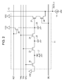
- Fig. 2 is a diagram illustrating an equivalent circuit in a pixel of Fig. 1.
- Fig. 3 is a cross-sectional view illustrating a pixel structure according to a first embodiment of the pixel.
- Fig. 4A is a plan view of the four adjacent pixels.
- Fig. 4B is a plan view of the four adjacent pixels.
- Fig. 5A is a diagram describing a transfer channel of a first transfer transistor.
- Fig. 5B is a diagram describing the transfer channel of the first transfer transistor.
- Fig. 1 is a block diagram illustrating an example of a schematic configuration of a solid state imaging device to which the present technology is applied.
- Fig. 2 is a diagram illustrating an equivalent circuit in a pixel of Fig. 1.
- Fig. 3 is a cross-sectional view illustrating a pixel structure according
- FIG. 6A is a diagram illustrating a potential of a photodiode and a memory unit in a depth direction of a substrate.
- Fig. 6B is a diagram illustrating the potential of the photodiode and the memory unit in the depth direction of the substrate.
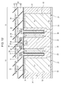
- Fig. 7 is a diagram describing a method for manufacturing a pixel.
- Fig. 8 is a diagram describing the method for manufacturing a pixel.
- Fig. 9 is a diagram describing the method for manufacturing a pixel.
- Fig. 10 is a diagram describing the method for manufacturing a pixel.
- Fig. 11 is a diagram describing the method for manufacturing a pixel.
- Fig. 12 is a diagram describing the method for manufacturing a pixel.
- FIG. 13 is a diagram describing the method for manufacturing a pixel.
- Fig. 14 is a cross-sectional view illustrating a pixel structure according to a second embodiment of the pixel.
- Fig. 15 is a cross-sectional view illustrating a pixel structure according to a third embodiment of the pixel.
- Fig. 16 is a cross-sectional view illustrating a pixel structure according to a fourth embodiment of the pixel.
- Fig. 17 is a block diagram illustrating a configuration example of an imaging apparatus as an electronic apparatus to which the present technology is applied.
- Example of an overall configuration of a solid state imaging device 2.
- Example of a circuit configuration of a pixel 3.
- Pixel structure according to a first embodiment (example of the configuration that a first transfer transistor and a memory unit are longitudinal types and a second transfer transistor is a flat surface type) 4.
- Plan view of the pixel 5.
- Features of the pixel 6.
- Method for manufacturing a pixel 7.
- Pixel structure according to a second embodiment (example of the configuration that the second transfer transistor is also the longitudinal type)
- Pixel structure according to a third embodiment (example of the configuration that the first transfer transistor passes through)
- Pixel structure according to a fourth embodiment (example of the configuration that a depth of the first transfer transistor is deeper than the depth of the second transfer transistor) 10.
- FIG. 1 is a block diagram illustrating an example of an overall configuration of a solid state imaging device to which the present technology is applied.
- a solid state imaging device 1 of Fig. 1 is configured of a timing control unit 2, a vertical scanning circuit 3, a pixel array unit 4, a constant current source circuit 5, a reference signal generation unit 6, a column AD conversion unit 7, a horizontal scanning circuit 8, a horizontal output line 9, and an output circuit 10.
- the timing control unit 2 Based on a master clock of a predetermined frequency, the timing control unit 2 supplies a clock signal and a timing signal which are necessary for a predetermined operation, to the vertical scanning circuit 3 and the horizontal scanning circuit 8. For example, the timing control unit 2 supplies the timing signal for a shutter operation and a readout operation of a pixel 11, to the vertical scanning circuit 3 and the horizontal scanning circuit 8. Furthermore, an illustration thereof is omitted, but the timing control unit 2 supplies the clock signal and the timing signal which are necessary for the predetermined operation, to the reference signal generation unit 6 and the column AD conversion unit 7 or the like.
- the vertical scanning circuit 3 sequentially supplies a signal which controls an output of a pixel signal, to each pixel 11 which is lined up in a vertical direction of the pixel array unit 4, at a predetermined timing.
- a plurality of the pixels 11 are arranged in a two-dimensional array shape (row and column shape).
- the plurality of the pixels 11 which are arranged in the two-dimensional array shape are connected to the vertical scanning circuit 3 by a row unit, by a horizontal signal line 12.
- the plurality of the pixels 11 which are arranged in the same row within the pixel array unit 4 are connected to the vertical scanning circuit 3, with one horizontal signal line 12.
- the horizontal signal line 12 is shown as one wiring, but is not limited to one.
- the plurality of the pixels 11 which are arranged in the two-dimensional array shape are connected to the horizontal scanning circuit 8 by a column unit, by a vertical signal line 13.
- the plurality of the pixels 11 which are arranged in the same column within the pixel array unit 4 are connected to the horizontal scanning circuit 8, with one vertical signal line 13.
- each pixel 11 within the pixel array unit 4 outputs the pixel signal according to a charge which is accumulated therein, to the vertical signal line 13.
- a detailed circuit configuration of the pixel 11 will be described later with reference to Fig. 2.
- the constant current source circuit 5 includes a plurality of load MOSs 14, and one load MOS 14 is connected to one vertical signal line 13. A bias voltage is applied to a gate of the load MOS 14, and a source is grounded.
- the load MOS 14 configures a transistor and a source follower circuit within the pixel 11 which is connected through the vertical signal line 13.
- the reference signal generation unit 6 is configured to include a Digital to Analog Converter (DAC) 6a, generates a reference signal of a ramp (RAMP) waveform, and supplies the reference signal to the column AD conversion unit 7, according to the clock signal from the timing control unit 2.
- DAC Digital to Analog Converter
- RAMP ramp
- a plurality of Analog-Digital Converters (ADCs) 15 which are made one by one for each column of the pixel array unit 4, are included in the column AD conversion unit 7. Therefore, the plurality of the pixels 11, one load MOS 14, and one ADC 15 are connected to one vertical signal line 13.
- ADCs Analog-Digital Converters
- the ADC 15 performs a Correlated Double Sampling; correlative double sampling (CDS) process of the pixel signal which is supplied through the vertical signal line 13 from the pixel 11 of the same column, and further performs an AD conversion process.
- CDS Correlative double sampling
- Each ADC 15 temporarily stores pixel data after the AD conversion, and outputs the pixel data to the horizontal output line 9, in accordance with a control of the horizontal scanning circuit 8.
- the horizontal scanning circuit 8 sequentially outputs the pixel data which is stored in the plurality of the ADCs 15, to the horizontal output line 9, at the predetermined timing.
- the horizontal output line 9 is connected to the output circuit (amplifier circuit) 10, and the pixel data which is output from each ADC 15 after the AD conversion, is output to an outside of the solid state imaging device 1 from the output circuit 10 through the horizontal output line 9.
- the output circuit 10 only performs buffering
- the output circuit 10 performs various digital signal process such as a black level adjustment and a variation correction in a column.
- the solid state imaging device 1 which is configured as described above, is a CMOS image sensor that is called a column AD system in which the ADCs 15 to perform the CDS process and the AD conversion process are arranged for each vertical column.
- the pixel 11 includes a photodiode 21 as a photoelectric conversion device, a first transfer transistor 22, a memory unit (MEM) 23, a second transfer transistor 24, a Floating Diffusion (FD) 25, a reset transistor 26, an amplification transistor 27, a selection transistor 28, and a discharge transistor 29.
- a photodiode 21 as a photoelectric conversion device
- a first transfer transistor 22 a memory unit (MEM) 23
- MEM memory unit
- FD Floating Diffusion
- FD Floating Diffusion
- reset transistor 26 an amplification transistor 27, a selection transistor 28, and a discharge transistor 29.
- the photodiode 21 is a photoelectric conversion unit that generates the charge (signal charge) according to an amount of light which is received, and accumulates the charge.
- An anode terminal of the photodiode 21 is grounded, and a cathode terminal thereof is connected to the memory unit 23 through the first transfer transistor 22. Moreover, the cathode terminal of the photodiode 21 is also connected to the discharge transistor 29.
- the first transfer transistor 22 When the first transfer transistor 22 is turned on by a transfer signal TRX, the first transfer transistor 22 reads out the charge which is generated by the photodiode 21, and transfers the charge to the memory unit 23. While the charge is transferred to the FD 25, the memory unit 23 is a charge accumulation unit that temporarily accumulates the charge.
- the second transfer transistor 24 When the second transfer transistor 24 is turned on by a transfer signal TRG, the second transfer transistor 24 transfers the charge which is held in the memory unit 23, to the FD 25.
- the FD 25 is a charge holding unit that holds the charge which is read out from the memory unit 23 in order to read out the charge as a signal.
- the reset transistor 26 is turned on by a reset signal RST, the charge which is held in the FD 25 is discharged to a constant voltage source VDD, and thereby the reset transistor 26 resets a potential of the FD 25.
- the amplification transistor 27 outputs the pixel signal according to the potential of the FD 25. That is, the amplification transistor 27 configures the load MOS 14 as a constant current source, and the source follower circuit, and the pixel signal that shows a level according to the charge which is held in the FD 25, is output to the ADC 15 through the selection transistor 28 from the amplification transistor 27.
- the selection transistor 28 When the pixel 11 is selected by a selection signal SEL, the selection transistor 28 is turned on, and outputs the pixel signal of the pixel 11, to the ADC 15 through the vertical signal line 13.
- the discharge transistor 29 When the discharge transistor 29 is turned on by a discharge signal OFG, the discharge transistor 29 discharges the unnecessary charge which is accumulated in the photodiode 21, to the constant voltage source VDD.
- the transfer signals TRX and TRG, the reset signal RST, the selection signal SEL, and the discharge signal OFG are controlled by the vertical scanning circuit 3, and are supplied through the horizontal signal line 12 (Fig. 1).
- the discharge signal OFG having a High level is supplied to the discharge transistor 29, and thereby the discharge transistor 29 is turned on, the charge which is accumulated in the photodiode 21 is discharged to the constant voltage source VDD, and the photodiode 21 is reset.
- the discharge transistor 29 After resetting the photodiode 21, the discharge transistor 29 is turned off by the discharge signal OFG having a Low level, and the exposure is started in all pixels.
- the first transfer transistor 22 When a predetermined exposure time which is set in advance passes, in all the pixels of the pixel array unit 4, the first transfer transistor 22 is turned on by the first transfer signal TRX, and the charge which is accumulated in the photodiode 21, is transferred to the memory unit 23.
- the charge which is held in the memory unit 23 of each pixel 11 is sequentially read out in the ADC 15, by a row unit.
- the second transfer transistors 24 of the pixel 11 in the row which is read out is turned on by the second transfer signal TRG, and the charge which is held in the memory unit 23 is transferred to the FD 25. Therefore, the selection transistor 28 is turned on by the selection signal SEL, and thereby the signal that shows the level according to the charge which is held in the FD 25, is output to the ADC 15 through the selection transistor 28 from the amplification transistor 27.
- Pixel structure according to a first embodiment The pixel 11 can adopt any one of pixel structures which are shown as a first embodiment to a fourth embodiment in the following. First, the pixel 11 according to the first embodiment will be described.
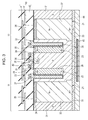
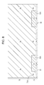
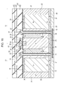
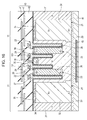
- Fig. 3 is a cross-sectional view illustrating the pixel structure according to the first embodiment of the pixel 11.
- the cross-sectional view of the structure of the pixel 11 which is shown in Fig. 3, is the cross-sectional view in case of sharing the FD 25 with the plurality of the pixels 11, and shows the cross-sectional view of the two adjacent pixels which share the FD 25.
- a lower side in the drawing is a rear surface side of a semiconductor substrate which is a light incidence side
- an upper side in the drawing corresponds to a surface side of the semiconductor substrate on which a wiring layer is formed. Therefore, the pixel 11 shown in Fig. 3 has the pixel structure of a rear surface irradiation type.
- each pixel 11 for example, within a P-type (first conductivity type) semiconductor region (semiconductor substrate) 31, an N-type (second conductivity type) semiconductor region 32 is formed, and thereby the photodiode 21 is formed.
- the region of the substrate rear surface side (lower side in the drawing) is adjusted to the N-type (N+) semiconductor region having a high concentration
- the region of the substrate surface side (upper side in the drawing) is adjusted to the N-type (N-) semiconductor region having a low concentration.
- a P-type (P+) semiconductor region 33 of which the concentration is higher than that of an inside region is formed.
- a P-type (P+) semiconductor region 34 having a high concentration is formed.
- a gate insulating film 35 is formed by silicon oxide (SiO 2 ) or the like.
- an N-type (N+) semiconductor region 36 having a high concentration which is the FD 25, is formed.
- a gate electrode 37 of the first transfer transistor 22 is formed to be buried up to a predetermined depth from the interface of the substrate surface side.
- the transistor of which the gate electrode is formed to be buried up to the predetermined depth from the interface of the substrate surface side is referred to as a longitudinal type transistor.
- an N-type semiconductor region 38 which is the memory unit 23 is formed on the FD 25 side which is opposite to the photodiode 21 side of the gate electrode 37 of the first transfer transistor 22, an N-type semiconductor region 38 which is the memory unit 23 is formed. Accordingly, the memory unit 23 is formed at a distant position from the FD 25 in a flat surface direction. Moreover, within the N-type semiconductor region 38 which is the memory unit 23, the region of the substrate rear surface side is adjusted to the N-type (N-) semiconductor region having a low concentration, and the region of the substrate surface side is adjusted to the N-type (N+) semiconductor region having a high concentration.
- a P-type (P+) semiconductor region 39 having a high concentration is formed between the N-type semiconductor region 38 which is the memory unit 23, and the gate insulating film 35.
- a gate electrode 40 of the second transfer transistor 24 is formed.
- a metal material having a light shielding capability such as tungsten (W) and copper (Cu) is used.
- tungsten (W) and copper (Cu) is used in the gate electrode 37 and the gate electrode 40.
- polysilicon (Poly-Si) may be also used in the gate electrode 37 and the gate electrode 40.
- a multilayer wiring layer 43 which is made up of a plurality of wiring layers 41 and an interlayer insulating film 42, is formed.
- a flattening film 44 is formed, and a light shielding film 45 is formed on the partial region within the flattening film 44.
- the light shielding film 45 is formed at the position to prevent the incidence of the light.
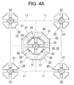
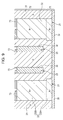
- Fig. 4A is a plan view which is taken when seen the four adjacent pixels 11 from the multilayer wiring layer 43 side.
- the N-type (N+) semiconductor region 36 having a high concentration as the FD 25 is arranged, and the solid state imaging device 1 adopts the configuration of arranging to share the one FD 25 with the four adjacent pixels 11.
- a dashed line within the gate electrode 37 of the first transfer transistor 22, shows the region where the gate electrode 37 is buried in the P-type semiconductor region 31.
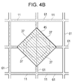
- Fig. 4B is a plan view which is taken when seen the flat surface in which the light shielding film 45 of the four adjacent pixels 11 is formed, from the light incidence side.
- the light shielding film 45 is formed in a flat surface, up to the outside of the gate electrode 37 of the first transfer transistor 22 which is dug in a depth direction, and thereby it is possible to prevent the incidence of the light in the N-type semiconductor region 38 which is the memory unit 23, and the N-type (N+) semiconductor region 36 having a high concentration which is the FD 25.
- an interpixel light shielding film 61 for preventing the incidence of the light from the adjacent pixels 11 is formed of the same material as the light shielding film 45.
- the N-type semiconductor region 38 as the memory unit 23 is formed in a longitudinally long shape along a side wall of the gate electrode 37 of the first transfer transistor 22 of the longitudinal type.
- the gate electrode 37 of the first transfer transistor 22 is formed of the material having a light shielding capability, it is possible to shield the incident light from the photodiode 21.
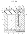
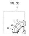
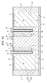
- FIGs. 5A and 5B are diagrams describing a transfer channel of the first transfer transistor 22.
- the charge which is accumulated in the N-type semiconductor region 32 as the photodiode 21, is transferred to the N-type semiconductor region 38 of the memory unit 23 through a bottom portion of the gate electrode 37 of the first transfer transistor 22. Furthermore, as shown in Fig. 5B, some of the charge is also transferred to the N-type semiconductor region 38 from a side of the gate electrode 37. However, the primary transfer channel of the charge is the bottom potion of the gate electrode 37.
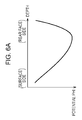
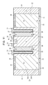
- Fig. 6A is a diagram illustrating the potential of the N-type semiconductor region 32 which is the charge accumulation region of the photodiode 21 in the depth direction of the substrate.
- the region of the substrate rear surface side is adjusted to the N-type (N+) semiconductor region having a high concentration, and the region of the substrate surface side is adjusted to the N-type (N-) semiconductor region having a low concentration.
- the potential becomes high.
- the charge is mainly accumulated in the substrate rear surface side.
- the transfer of the charge to the memory unit 23 from the photodiode 21, is easier.
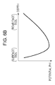
- Fig. 6B is a diagram illustrating the potential of the N-type semiconductor region 38 which is the memory unit 23 in the depth direction of the substrate, when the first transfer transistor 22 is turned on.
- the region of the substrate rear surface side is adjusted to the N-type (N-) semiconductor region having a low concentration, and the region of the substrate surface side is adjusted to the N-type (N+) semiconductor region having a high concentration.
- the potential becomes high.
- the charge is mainly accumulated in the substrate surface side.
- the transfer of the charge to the FD 25 from the memory unit 23, is easier.
- the configuration that can achieve the refinement thereof and facilitate the transfer of the charge by adjusting the impurity concentration of the charge accumulation region, is adopted.
- SOI Silicon On Insulator
- an N-type ion such as phosphorus (P) and arsenic (As) is injected, and thereby an N-type (N+) semiconductor region 32A having a high concentration is formed, within the N-type semiconductor region 32 which is the charge accumulation region of the photodiode 21.
- an N-type silicon layer 72 is formed by epitaxial growth. Moreover, instead of the process which is described with reference to Fig. 7 and Fig. 8, into the silicon substrate of a thick film, the ion is injected at high acceleration energy, and thereby it is possible to form the structure which is similar to Fig. 8.
- the N-type ion is injected, and thereby an N-type (N-) semiconductor region 32B having a low concentration on the substrate surface side of the photodiode 21, is formed.
- the semiconductor region 32 of the photodiode 21 which is made up of the N-type (N+) semiconductor region 32A having a high concentration and the N-type (N-) semiconductor region 32B having a low concentration, is completed.
- the N-type impurity concentration of the semiconductor region 32B is higher than that of the N-type silicon layer 72.
- the N-type ion is injected into the predetermined region of the N-type silicon layer 72, and thereby the N-type semiconductor region 38 which is the memory unit 23, is also formed.
- the P-type ion is injected, and thereby the P-type semiconductor region 31 is formed.
- the N-type semiconductor region 32B of the photodiode 21, and only the upper portion of the N-type semiconductor region 38 of the memory unit 23 become an N-type semiconductor region 73 which is formed by the epitaxial growth.
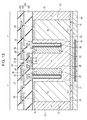
- the predetermined region of the P-type semiconductor region 31 between the semiconductor region 32 of the photodiode 21, and the semiconductor regions 38 of the memory unit 23, are dug up to the depth which is almost the same as the semiconductor region 38 of the memory unit 23, from the substrate surface side. Therefore, after the gate insulating film 35 is formed on the entire surface of the substrate surface side, the gate electrode 37 of the first transfer transistor 22, and the gate electrode 40 of the second transfer transistor 24 are formed.
- the P-type ion is injected with respect to the semiconductor region 32 of the photodiode 21 and the N-type semiconductor region 73 in the upper portion of the semiconductor region 38 of the memory unit 23, and thereby the P-type (P+) semiconductor regions 34 and 39 having a high concentration, are formed.
- the N-type ion is injected with respect to the P-type semiconductor region 31 between the gate electrodes 40 of the two second transfer transistors 24 of the two adjacent pixels, and thereby N-type (N+) semiconductor region 36 having a high concentration as the FD 25 is formed.
- the N-type (N+) semiconductor region 52 for discharging the charge in Figs. 4A and 4B, is also formed at the same time.
- the N-type ion injection to form the N-type (N+) semiconductor region 36 having a high concentration as the FD 25 is also injected into the upper portion of the semiconductor region 38 of the memory unit 23, and with respect to the semiconductor region 38, a concentration difference which varies in the depth direction is formed.
- the process of the N-type ion injection and the P-type ion injection which is described with reference to Fig. 11, may be performed before forming the gate insulating film 35, the gate electrode 37 of the first transfer transistor 22, and the gate electrode 40 of the second transfer transistor 24 as described with reference to Fig. 10.
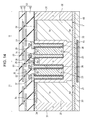
- the multilayer wiring layer 43 which is made up of the plurality of the wiring layer 41 and the interlayer insulating film 42, are formed. Therefore, as shown in Fig. 13, after the flattening film 44 and the light shielding film 45 are formed on the substrate rear surface side, the color filter and the on-chip lens which are not shown in the drawing, are formed on the further lower side (light incidence side) of the flattening film 44.
- Pixel structure according to a second embodiment Next, the pixel 11 according to a second embodiment will be described.
- Fig. 14 is a cross-sectional view illustrating the pixel structure according to the second embodiment of the pixel 11.
- both of the first transfer transistor 22 and the second transfer transistor 24 can be formed in the longitudinal type transistor which is dug up to the depth which is almost the same as the memory unit 23 including the gate electrode of the longitudinally long shape.
- Pixel structure according to a third embodiment Next, the pixel 11 according to a third embodiment will be described.
- Fig. 15 is a cross-sectional view illustrating the pixel structure according to the third embodiment of the pixel 11.
- the point that a gate electrode 91 of the first transfer transistor 22 is not formed up to the depth which is almost the same as the N-type semiconductor region 38 of the memory unit 23 and passes through the P-type semiconductor region 31, is different from the first embodiment.
- the transfer channel of the charge to the memory unit 23 from the photodiode 21 is only the side wall of the first transfer transistor 22 shown in Fig. 5B.
- Pixel structure according to a fourth embodiment Next, the pixel 11 according to a fourth embodiment will be described.
- Fig. 16 is a cross-sectional view illustrating the pixel structure according to the fourth embodiment of the pixel 11.
- the point that the second transfer transistor 24 is not the flat surface type and is formed in the longitudinal type, is different from the first embodiment. Furthermore, the point that a gate electrode 101 of the second transfer transistor 24 is not formed up to the depth which is almost the same as the N-type semiconductor region 38 which is the memory unit 23 and is formed up to the depth in the middle of the N-type semiconductor region 38, is different from the second embodiment of Fig. 14.
- the depth in the gate electrode 37 of the first transfer transistor 22 which is the longitudinal type transistor is different from the depth in the gate electrode 101 of the second transfer transistor 24.
- the depth in the gate electrode 101 of the second transfer transistor 24 may be good if the depth in the gate electrode 101 of the second transfer transistor 24 is not deeper than the depth in the N-type semiconductor region 38 of the memory unit 23.
- the first transfer transistor 22 is formed in the longitudinal type according to any one of the second embodiment to the fourth embodiment described above, it is possible to achieve the refinement of the pixel, and to realize the structure which can be also applied to the rear surface irradiation type.
- the present technology is not limited to an application to the solid state imaging device. That is, the present technology can be generally applied with respect to an electronic apparatus using the solid state imaging device in an image capturing unit (photoelectric conversion unit) such as an imaging apparatus of a digital still camera, a video camera or the like, a mobile terminal apparatus having an imaging function, and a copy machine using the solid state imaging device in an image reading unit.
- the solid state imaging device may be formed in the form as one chip, and may be formed in the form of a module shape having an imaging function which is packaged with an imaging unit, a signal processing unit or an optical system together.
- Fig. 17 is a block diagram illustrating a configuration example of the imaging apparatus as the electronic apparatus to which the present technology is applied.
- An imaging apparatus 200 of Fig. 17, includes an optical unit 201 which is made up of a lens group and the like, a solid state imaging device (image pickup device) 202 in which each configuration of the pixel 11 described above is adopted, and a DSP (Digital Signal Processor) circuit 203 which is a camera signal processing circuit. Moreover, the imaging apparatus 200 also includes a frame memory 204, a display unit 205, a recording unit 206, an operation unit 207, and a power supply unit 208. The DSP circuit 203, the frame memory 204, the display unit 205, the recording unit 206, the operation unit 207, and the power supply unit 208 are connected to each other through a bus line 209.
- the optical unit 201 captures the incident light (image light) from a subject, and forms an image on an imaging surface of the solid state imaging device 202.
- the solid state imaging device 202 converts a light amount of the incident light with which the image is formed on the imaging surface by the optical unit 201, into an electrical signal by a pixel unit, and outputs the converted signal as a pixel signal.
- the solid state imaging device 202 the solid state imaging device 1 of Fig. 1 may be used.
- the display unit 205 is made up of a panel type display device such as liquid crystal panel and an organic EL (Electro Luminescence) panel, and displays a moving image or a still image of which the image is imaged by the solid state imaging device 202.
- the recording unit 206 records the moving image or the still image of which the image is imaged by the solid state imaging device 202, on a recording medium such as a hard disk and a semiconductor memory.
- the operation unit 207 issues an operation instruction for various functions which are held in the imaging apparatus 200.
- the power supply unit 208 appropriately supplies various power sources which are operation power supplies of the DSP circuit 203, the frame memory 204, the display unit 205, the recording unit 206, and the operation unit 207, with respect to the supply targets.
- the present technology is not limited to the application to the solid state imaging device that detects distribution of the incident light amount of the visible light, and images the distribution thereof as an image.
- the present technology can be generally applied with respect to the solid state imaging device such as the solid state imaging device imaging the distribution of the incident amount of infrared rays, X-ray, particles or the like as an image, and the solid state imaging device (physical quantity distribution detection device) such as a fingerprint detection sensor which detects the distribution of other physical quantity such as pressure and electrostatic capacity and images the distribution thereof as an image, in a broad sense.
- the pixel structure of the rear surface irradiation type is described, but the present technology can be also applied to the pixel structure of the surface irradiation type.
- the solid state imaging device setting the first conductivity type as P-type, the second conductivity type as N-type, and an electron as signal charge is described, but the present technology can be also applied to the solid state imaging device setting a positive hole as signal charge. That is, it is possible to configure each semiconductor region described above in the semiconductor region of the reverse conductivity type setting the first conductivity type as N-type and the second conductivity type as P-type.
- a solid state imaging device comprising: a pixel, including: a photoelectric conversion unit; a charge accumulation unit that accumulates the charge which is generated by the photoelectric conversion unit; a first transfer transistor that transfers the charge of the photoelectric conversion unit to the charge accumulation unit; wherein a gate electrode of the first transfer transistor extends from a first surface of a semiconductor substrate that is opposite from a light receiving surface of the semiconductor substrate to a predetermined first depth within the semiconductor substrate, and wherein the charge accumulation unit extends to a second depth adjacent a side wall of the gate electrode of the first transfer transistor which is buried within the semiconductor substrate.
- the solid state imaging device further comprising: a charge holding unit, wherein the charge holding unit is separated from the charge accumulation unit in a direction parallel to the light receiving surface of the semiconductor substrate.
- a charge holding unit wherein the charge holding unit is separated from the charge accumulation unit in a direction parallel to the light receiving surface of the semiconductor substrate.
- the charge accumulation unit is formed on a charge holding unit side of the first transfer transistor, and wherein the photoelectric conversion unit is on an opposite side of the first transfer transistor.
- the charge accumulation unit is adjusted so as to make a potential of a light incident side of the charge accumulation unit low, when the first transfer transistor is turned on.
- the solid state imaging device wherein the photoelectric conversion unit is adjusted so as to make a potential of a light incident side high.
- the solid state imaging device further comprising: a charge holding unit; and a light shielding film on a light incident side of the charge accumulation unit and the charge holding unit.
- a transfer channel of the first transfer transistor is formed in a vicinity of a side wall of the gate electrode.
- a transfer channel of the first transfer transistor is formed in a vicinity of a bottom portion of the gate electrode.
- the gate electrode of the first transfer transistor is formed of a material having a light shielding capability.
- the solid state imaging device according to the above (1), further comprising: a charge holding unit that holds the charge in order to read out the charge as a signal; and a second transfer transistor that transfers the charge of the charge accumulation unit to the charge holding unit.
- a gate electrode of the second transfer transistor is formed to be buried in a depth direction of the semiconductor substrate.
- a depth of the gate electrode of the second transfer transistor is the same as a depth of the gate electrode of the first transfer transistor.
- a depth of the gate electrode of the second transfer transistor is shallower than a depth of the gate electrode of the first transfer transistor.
- a method for manufacturing a solid state imaging device comprising: forming a pixel including a photoelectric conversion unit that generates a charge according to an amount of light which is received; forming a charge accumulation unit that accumulates the charge which is generated by the photoelectric conversion unit; forming a first transfer transistor that transfers the charge of the photoelectric conversion unit to the charge accumulation unit; forming a gate electrode of the first transfer transistor, wherein the gate electrode of the first transfer transistor extends from a first surface of a semiconductor substrate that is opposite from a light receiving surface of the semiconductor substrate to a predetermined first depth within the semiconductor substrate, and wherein the charge accumulation unit extends to a second depth adjacent a side wall of the gate electrode of the first transfer transistor which is buried within the semiconductor substrate.
- An electronic apparatus comprising: a solid state imaging device, wherein the solid state imaging device includes a pixel including: a photoelectric conversion unit; a charge accumulation unit that accumulates the charge which is generated by the photoelectric conversion unit, a first transfer transistor that transfers the charge of the photoelectric conversion unit to the charge accumulation unit, wherein a gate electrode of the first transfer transistor extends from a first surface of a semiconductor substrate that is opposite from a light receiving surface of the semiconductor substrate to a predetermined first depth within the semiconductor substrate, and wherein the charge accumulation unit extends to a second depth adjacent a side wall of the gate electrode of the first transfer transistor which is buried within the semiconductor substrate.
- a charge holding unit that holds the charge in order to read out the charge as a signal
- a second transfer transistor that transfers the charge of the charge accumulation unit to the charge holding unit.
- Solid state imaging device 4 Pixel array unit 21 Photodiode 22 First transfer transistor 23 Memory unit (MEM) 24 Second transfer transistor 25 FD (floating diffusion) 200 Imaging apparatus 202 Solid state imaging device
Abstract
Description
This application claims the benefit of Japanese Priority Patent Application JP 2013-220141 filed October 23, 2013, the entire contents of which are incorporated herein by reference.
1. Example of an overall configuration of a solid state imaging device
2. Example of a circuit configuration of a pixel
3. Pixel structure according to a first embodiment (example of the configuration that a first transfer transistor and a memory unit are longitudinal types and a second transfer transistor is a flat surface type)
4. Plan view of the pixel
5. Features of the pixel
6. Method for manufacturing a pixel
7. Pixel structure according to a second embodiment (example of the configuration that the second transfer transistor is also the longitudinal type)
8. Pixel structure according to a third embodiment (example of the configuration that the first transfer transistor passes through)
9. Pixel structure according to a fourth embodiment (example of the configuration that a depth of the first transfer transistor is deeper than the depth of the second transfer transistor)
10. Configuration example of an electronic apparatus to which the present technology is applied
Fig. 1 is a block diagram illustrating an example of an overall configuration of a solid state imaging device to which the present technology is applied.
Fig. 2 shows an equivalent circuit of the
The
Fig. 4A is a plan view which is taken when seen the four
Figs. 5A and 5B are diagrams describing a transfer channel of the
Next, referring to Fig. 7 to Fig. 13, a method for manufacturing the
Next, the
Next, the
Next, the
The present technology is not limited to an application to the solid state imaging device. That is, the present technology can be generally applied with respect to an electronic apparatus using the solid state imaging device in an image capturing unit (photoelectric conversion unit) such as an imaging apparatus of a digital still camera, a video camera or the like, a mobile terminal apparatus having an imaging function, and a copy machine using the solid state imaging device in an image reading unit. The solid state imaging device may be formed in the form as one chip, and may be formed in the form of a module shape having an imaging function which is packaged with an imaging unit, a signal processing unit or an optical system together.
(1) A solid state imaging device, comprising: a pixel, including: a photoelectric conversion unit;
a charge accumulation unit that accumulates the charge which is generated by the photoelectric conversion unit;
a first transfer transistor that transfers the charge of the photoelectric conversion unit to the charge accumulation unit;
wherein a gate electrode of the first transfer transistor extends from a first surface of a semiconductor substrate that is opposite from a light receiving surface of the semiconductor substrate to a predetermined first depth within the semiconductor substrate, and
wherein the charge accumulation unit extends to a second depth adjacent a side wall of the gate electrode of the first transfer transistor which is buried within the semiconductor substrate.
(2) The solid state imaging device according to the above (1), further comprising: a charge holding unit, wherein the charge holding unit is separated from the charge accumulation unit in a direction parallel to the light receiving surface of the semiconductor substrate.
(3) The solid state imaging device according to the above (1), wherein the charge accumulation unit is formed on a charge holding unit side of the first transfer transistor, and wherein the photoelectric conversion unit is on an opposite side of the first transfer transistor.
(4) The solid state imaging device according to the above (1), wherein the charge accumulation unit is adjusted so as to make a potential of a light incident side of the charge accumulation unit low, when the first transfer transistor is turned on.
(5) The solid state imaging device according to the above (1), wherein the photoelectric conversion unit is adjusted so as to make a potential of a light incident side high.
(6) The solid state imaging device according to the above (1), further comprising: a charge holding unit; and
a light shielding film on a light incident side of the charge accumulation unit and the charge holding unit.
(7) The solid state imaging device according to the above (1), wherein a transfer channel of the first transfer transistor is formed in a vicinity of a side wall of the gate electrode.
(8) The solid state imaging device according to the above (1), wherein a transfer channel of the first transfer transistor is formed in a vicinity of a bottom portion of the gate electrode.
(9) The solid state imaging device according to the above (1), wherein the gate electrode of the first transfer transistor is formed of a material having a light shielding capability.
(10) The solid state imaging device according to the above (1), further comprising: a charge holding unit that holds the charge in order to read out the charge as a signal; and
a second transfer transistor that transfers the charge of the charge accumulation unit to the charge holding unit.
(11) The solid state imaging device according to the above (10), wherein a gate electrode of the second transfer transistor is formed to be buried in a depth direction of the semiconductor substrate.
(12) The solid state imaging device according to the above (11), wherein a depth of the gate electrode of the second transfer transistor is the same as a depth of the gate electrode of the first transfer transistor.
(13) The solid state imaging device according to the above (11), wherein a depth of the gate electrode of the second transfer transistor is shallower than a depth of the gate electrode of the first transfer transistor.
(14) The solid state imaging device according to the above (10), wherein the gate electrode of the first transfer transistor passes through the semiconductor substrate.
(15) The solid state imaging device according to the above (14), wherein a gate electrode of the second transfer transistor is formed to be buried in a depth direction of the semiconductor substrate, and wherein a depth of the gate electrode of the second transfer transistor is shallower than a depth of the gate electrode of the first transfer transistor.
(16) The solid state imaging device according to the above (1), wherein the charge accumulation unit is smaller than the photoelectric conversion unit in a dimension parallel to a light incident side of the semiconductor substrate.
(17) The solid state imaging device according to the above (1), wherein the charge holding unit is configured so as to be shared with other pixels which are adjacent to the pixel.
(18) The solid state imaging device of the above (1), wherein the first depth of the gate electrode of the first transfer transistor is the same as the second depth of the charge accumulation unit.
(19) A method for manufacturing a solid state imaging device, comprising: forming a pixel including a photoelectric conversion unit that generates a charge according to an amount of light which is received;
forming a charge accumulation unit that accumulates the charge which is generated by the photoelectric conversion unit;
forming a first transfer transistor that transfers the charge of the photoelectric conversion unit to the charge accumulation unit;
forming a gate electrode of the first transfer transistor, wherein the gate electrode of the first transfer transistor extends from a first surface of a semiconductor substrate that is opposite from a light receiving surface of the semiconductor substrate to a predetermined first depth within the semiconductor substrate, and
wherein the charge accumulation unit extends to a second depth adjacent a side wall of the gate electrode of the first transfer transistor which is buried within the semiconductor substrate.
(20) The method of the above (19), further comprising: forming a charge holding unit that holds the charge in order to read out the charge as a signal, and a second transfer transistor that transfers the charge of the charge accumulation unit to the charge holding unit.
(21) An electronic apparatus, comprising: a solid state imaging device,
wherein the solid state imaging device includes a pixel including: a photoelectric conversion unit;
a charge accumulation unit that accumulates the charge which is generated by the photoelectric conversion unit,
a first transfer transistor that transfers the charge of the photoelectric conversion unit to the charge accumulation unit,
wherein a gate electrode of the first transfer transistor extends from a first surface of a semiconductor substrate that is opposite from a light receiving surface of the semiconductor substrate to a predetermined first depth within the semiconductor substrate, and
wherein the charge accumulation unit extends to a second depth adjacent a side wall of the gate electrode of the first transfer transistor which is buried within the semiconductor substrate.
(22) The electronic apparatus of the above (21), further comprising: a charge holding unit that holds the charge in order to read out the charge as a signal, and
a second transfer transistor that transfers the charge of the charge accumulation unit to the charge holding unit.
(23) The electronic apparatus of the above (21), wherein the first depth of the gate electrode of the first transfer transistor is the same as the second depth of the charge accumulation unit.
4 Pixel array unit
21 Photodiode
22 First transfer transistor
23 Memory unit (MEM)
24 Second transfer transistor
25 FD (floating diffusion)
200 Imaging apparatus
202 Solid state imaging device
Claims (23)
- A solid state imaging device, comprising:
a pixel, including:
a photoelectric conversion unit;
a charge accumulation unit that accumulates the charge which is generated by the photoelectric conversion unit;
a first transfer transistor that transfers the charge of the photoelectric conversion unit to the charge accumulation unit;
wherein a gate electrode of the first transfer transistor extends from a first surface of a semiconductor substrate that is opposite from a light receiving surface of the semiconductor substrate to a predetermined first depth within the semiconductor substrate, and
wherein the charge accumulation unit extends to a second depth adjacent a side wall of the gate electrode of the first transfer transistor which is buried within the semiconductor substrate. - The solid state imaging device according to Claim 1, further comprising:
a charge holding unit, wherein the charge holding unit is separated from the charge accumulation unit in a direction parallel to the light receiving surface of the semiconductor substrate. - The solid state imaging device according to Claim 1, wherein the charge accumulation unit is formed on a charge holding unit side of the first transfer transistor, and wherein the photoelectric conversion unit is on an opposite side of the first transfer transistor.
- The solid state imaging device according to Claim 1, wherein the charge accumulation unit is adjusted so as to make a potential of a light incident side of the charge accumulation unit low, when the first transfer transistor is turned on.
- The solid state imaging device according to Claim 1, wherein the photoelectric conversion unit is adjusted so as to make a potential of a light incident side high.
- The solid state imaging device according to Claim 1, further comprising:
a charge holding unit; and
a light shielding film on a light incident side of the charge accumulation unit and the charge holding unit. - The solid state imaging device according to Claim 1, wherein a transfer channel of the first transfer transistor is formed in a vicinity of a side wall of the gate electrode.
- The solid state imaging device according to Claim 1, wherein a transfer channel of the first transfer transistor is formed in a vicinity of a bottom portion of the gate electrode.
- The solid state imaging device according to Claim 1, wherein the gate electrode of the first transfer transistor is formed of a material having a light shielding capability.
- The solid state imaging device according to Claim 1, further comprising:
a charge holding unit that holds the charge in order to read out the charge as a signal; and
a second transfer transistor that transfers the charge of the charge accumulation unit to the charge holding unit. - The solid state imaging device according to Claim 10, wherein a gate electrode of the second transfer transistor is formed to be buried in a depth direction of the semiconductor substrate.
- The solid state imaging device according to Claim 11, wherein a depth of the gate electrode of the second transfer transistor is the same as a depth of the gate electrode of the first transfer transistor.
- The solid state imaging device according to Claim 11, wherein a depth of the gate electrode of the second transfer transistor is shallower than a depth of the gate electrode of the first transfer transistor.
- The solid state imaging device according to Claim 10, wherein the gate electrode of the first transfer transistor passes through the semiconductor substrate.
- The solid state imaging device according to Claim 14, wherein a gate electrode of the second transfer transistor is formed to be buried in a depth direction of the semiconductor substrate, and wherein a depth of the gate electrode of the second transfer transistor is shallower than a depth of the gate electrode of the first transfer transistor.
- The solid state imaging device according to Claim 1, wherein the charge accumulation unit is smaller than the photoelectric conversion unit in a dimension parallel to a light incident side of the semiconductor substrate.
- The solid state imaging device according to Claim 1, wherein the charge holding unit is configured so as to be shared with other pixels which are adjacent to the pixel.
- The solid state imaging device of claim 1, wherein the first depth of the gate electrode of the first transfer transistor is the same as the second depth of the charge accumulation unit.
- A method for manufacturing a solid state imaging device, comprising:
forming a pixel including a photoelectric conversion unit that generates a charge according to an amount of light which is received;
forming a charge accumulation unit that accumulates the charge which is generated by the photoelectric conversion unit;
forming a first transfer transistor that transfers the charge of the photoelectric conversion unit to the charge accumulation unit;
forming a gate electrode of the first transfer transistor, wherein the gate electrode of the first transfer transistor extends from a first surface of a semiconductor substrate that is opposite from a light receiving surface of the semiconductor substrate to a predetermined first depth within the semiconductor substrate, and
wherein the charge accumulation unit extends to a second depth adjacent a side wall of the gate electrode of the first transfer transistor which is buried within the semiconductor substrate. - The method of claim 19, further comprising:
forming a charge holding unit that holds the charge in order to read out the charge as a signal, and a second transfer transistor that transfers the charge of the charge accumulation unit to the charge holding unit. - An electronic apparatus, comprising:
a solid state imaging device,
wherein the solid state imaging device includes a pixel including:
a photoelectric conversion unit;
a charge accumulation unit that accumulates the charge which is generated by the photoelectric conversion unit,
a first transfer transistor that transfers the charge of the photoelectric conversion unit to the charge accumulation unit,
wherein a gate electrode of the first transfer transistor extends from a first surface of a semiconductor substrate that is opposite from a light receiving surface of the semiconductor substrate to a predetermined first depth within the semiconductor substrate, and
wherein the charge accumulation unit extends to a second depth adjacent a side wall of the gate electrode of the first transfer transistor which is buried within the semiconductor substrate. - The electronic apparatus of claim 21, further comprising:
a charge holding unit that holds the charge in order to read out the charge as a signal, and
a second transfer transistor that transfers the charge of the charge accumulation unit to the charge holding unit. - The electronic apparatus of claim 21, wherein the first depth of the gate electrode of the first transfer transistor is the same as the second depth of the charge accumulation unit.
Priority Applications (5)
| Application Number | Priority Date | Filing Date | Title |
|---|---|---|---|
| KR1020217033619A KR102499590B1 (en) | 2013-10-23 | 2014-10-14 | Solid state imaging device and manufacturing method therefor, and electronic apparatus |
| US15/029,717 US9985068B2 (en) | 2013-10-23 | 2014-10-14 | Solid-state imaging device and manufacturing method therefor, and electronic apparatus |
| KR1020237004308A KR20230025932A (en) | 2013-10-23 | 2014-10-14 | Solid state imaging device and manufacturing method therefor, and electronic apparatus |
| KR1020247004618A KR20240023207A (en) | 2013-10-23 | 2014-10-14 | Solid state imaging device and manufacturing method therefor, and electronic apparatus |
| KR1020167009789A KR102318462B1 (en) | 2013-10-23 | 2014-10-14 | Solid state imaging device and manufacturing method therefor, and electronic apparatus |
Applications Claiming Priority (2)
| Application Number | Priority Date | Filing Date | Title |
|---|---|---|---|
| JP2013-220141 | 2013-10-23 | ||
| JP2013220141A JP6138661B2 (en) | 2013-10-23 | 2013-10-23 | Solid-state imaging device, manufacturing method thereof, and electronic device |
Publications (1)
| Publication Number | Publication Date |
|---|---|
| WO2015059898A1 true WO2015059898A1 (en) | 2015-04-30 |
Family
ID=51862495
Family Applications (1)
| Application Number | Title | Priority Date | Filing Date |
|---|---|---|---|
| PCT/JP2014/005203 WO2015059898A1 (en) | 2013-10-23 | 2014-10-14 | Solid state imaging device and manufacturing method therefor, and electronic apparatus |
Country Status (5)
| Country | Link |
|---|---|
| US (1) | US9985068B2 (en) |
| JP (1) | JP6138661B2 (en) |
| KR (4) | KR20240023207A (en) |
| TW (1) | TWI645551B (en) |
| WO (1) | WO2015059898A1 (en) |
Cited By (3)
| Publication number | Priority date | Publication date | Assignee | Title |
|---|---|---|---|---|
| US10483304B2 (en) | 2017-01-09 | 2019-11-19 | Samsung Electronics Co., Ltd. | Image sensor |
| WO2020116131A1 (en) * | 2018-12-03 | 2020-06-11 | Sony Semiconductor Solutions Corporation | Solid-state imaging element, method of manufacturing solid-state imaging element, and electronic device |
| US11330203B2 (en) | 2018-07-24 | 2022-05-10 | Sony Semiconductor Solutions Corporation | Imaging device and electronic device |
Families Citing this family (14)
| Publication number | Priority date | Publication date | Assignee | Title |
|---|---|---|---|---|
| JP6706481B2 (en) * | 2015-11-05 | 2020-06-10 | ソニーセミコンダクタソリューションズ株式会社 | Image sensor |
| KR102504887B1 (en) * | 2016-07-06 | 2023-03-02 | 소니 세미컨덕터 솔루션즈 가부시키가이샤 | Imaging element, method for producing imaging element, and electronic device |
| IT201600083804A1 (en) * | 2016-08-09 | 2018-02-09 | St Microelectronics Srl | PROCESS OF MANUFACTURE OF A SEMICONDUCTOR DEVICE INCLUDING A MICROELECTRCANICAL STRUCTURE AND AN ASSOCIATED INTEGRATED ELECTRONIC CIRCUIT AND ITS SEMICONDUCTOR DEVICE |
| JPWO2018083990A1 (en) * | 2016-11-02 | 2019-09-19 | ソニーセミコンダクタソリューションズ株式会社 | Imaging device, imaging device, and electronic device |
| FR3060250B1 (en) * | 2016-12-12 | 2019-08-23 | Commissariat A L'energie Atomique Et Aux Energies Alternatives | IMAGE SENSOR FOR CAPTURING A 2D IMAGE AND DEPTH |
| KR102473149B1 (en) | 2017-11-13 | 2022-12-02 | 에스케이하이닉스 주식회사 | Image sensor |
| WO2019202858A1 (en) * | 2018-04-16 | 2019-10-24 | ソニーセミコンダクタソリューションズ株式会社 | Imaging element and method of manufacturing imaging element |
| KR102446297B1 (en) * | 2018-05-02 | 2022-09-23 | 에스케이하이닉스 주식회사 | Image Sensor Including An Extra Transfer Transistor and An Extra Floating Diffusion Region |
| US11482550B2 (en) | 2018-07-31 | 2022-10-25 | Sony Semiconductor Solutions Corporation | Imaging device and electronic apparatus |
| US10566359B1 (en) * | 2018-08-22 | 2020-02-18 | Omnivision Technologies, Inc. | Variably biased isolation structure for global shutter pixel storage node |
| JP2020035916A (en) * | 2018-08-30 | 2020-03-05 | ソニーセミコンダクタソリューションズ株式会社 | Imaging apparatus and electronic equipment |
| KR102560775B1 (en) * | 2018-12-20 | 2023-07-28 | 삼성전자주식회사 | Image sensor |
| KR20210003492A (en) | 2019-07-02 | 2021-01-12 | 에스케이하이닉스 주식회사 | Image sensing device |
| US20230224602A1 (en) * | 2020-05-20 | 2023-07-13 | Sony Semiconductor Solutions Corporation | Solid-state imaging device |
Citations (3)
| Publication number | Priority date | Publication date | Assignee | Title |
|---|---|---|---|---|
| JP2010114273A (en) * | 2008-11-06 | 2010-05-20 | Sony Corp | Solid-state imaging device and electronic apparatus |
| US20110187911A1 (en) * | 2010-01-29 | 2011-08-04 | Sony Corporation | Solid-state imaging device, method of manufacturing the same, and electronic apparatus |
| WO2013088983A1 (en) * | 2011-12-12 | 2013-06-20 | ソニー株式会社 | Solid-state imaging device, method for driving solid-state imaging device, and electronic instrument |
Family Cites Families (14)
| Publication number | Priority date | Publication date | Assignee | Title |
|---|---|---|---|---|
| JP4341421B2 (en) * | 2004-02-04 | 2009-10-07 | ソニー株式会社 | Solid-state imaging device |
| US8445944B2 (en) * | 2004-02-04 | 2013-05-21 | Sony Corporation | Solid-state image pickup device |
| JP2006311515A (en) * | 2005-03-29 | 2006-11-09 | Konica Minolta Holdings Inc | Solid-state image-sensing device |
| KR101030263B1 (en) | 2006-11-30 | 2011-04-22 | 고쿠리츠 다이가꾸 호우진 시즈오까 다이가꾸 | Semiconductor range-finding element and solid-state imaging device |
| JP5568880B2 (en) | 2008-04-03 | 2014-08-13 | ソニー株式会社 | Solid-state imaging device, driving method of solid-state imaging device, and electronic apparatus |
| EP2133918B1 (en) * | 2008-06-09 | 2015-01-28 | Sony Corporation | Solid-state imaging device, drive method thereof and electronic apparatus |
| JP5374941B2 (en) * | 2008-07-02 | 2013-12-25 | ソニー株式会社 | Solid-state imaging device and electronic device |
| TWI445166B (en) * | 2008-11-07 | 2014-07-11 | Sony Corp | Solid-state imaging device, method for manufacturing solid-state imaging device, and electronic apparatus |
| JP5552768B2 (en) * | 2009-07-27 | 2014-07-16 | ソニー株式会社 | SOLID-STATE IMAGING DEVICE, ITS MANUFACTURING METHOD, AND ELECTRONIC DEVICE |
| JP5493669B2 (en) * | 2009-10-07 | 2014-05-14 | ソニー株式会社 | Solid-state imaging device, imaging device, and manufacturing method of solid-state imaging device |
| JP5581954B2 (en) * | 2010-10-07 | 2014-09-03 | ソニー株式会社 | Solid-state imaging device, method for manufacturing solid-state imaging device, and electronic apparatus |
| US9570489B2 (en) * | 2011-07-12 | 2017-02-14 | Sony Corporation | Solid state imaging device having impurity concentration on light receiving surface being greater or equal to that on opposing surface |
| JP2013098446A (en) * | 2011-11-04 | 2013-05-20 | Sony Corp | Solid-state imaging element, method for manufacturing solid-state imaging element, and electronic device |
| KR101968197B1 (en) * | 2012-05-18 | 2019-04-12 | 삼성전자주식회사 | Image sensor and method of forming the same |
-
2013
- 2013-10-23 JP JP2013220141A patent/JP6138661B2/en not_active Expired - Fee Related
-
2014
- 2014-09-18 TW TW103132308A patent/TWI645551B/en active
- 2014-10-14 KR KR1020247004618A patent/KR20240023207A/en active Application Filing
- 2014-10-14 WO PCT/JP2014/005203 patent/WO2015059898A1/en active Application Filing
- 2014-10-14 KR KR1020237004308A patent/KR20230025932A/en active IP Right Grant
- 2014-10-14 KR KR1020167009789A patent/KR102318462B1/en active IP Right Grant
- 2014-10-14 US US15/029,717 patent/US9985068B2/en active Active
- 2014-10-14 KR KR1020217033619A patent/KR102499590B1/en active IP Right Grant
Patent Citations (3)
| Publication number | Priority date | Publication date | Assignee | Title |
|---|---|---|---|---|
| JP2010114273A (en) * | 2008-11-06 | 2010-05-20 | Sony Corp | Solid-state imaging device and electronic apparatus |
| US20110187911A1 (en) * | 2010-01-29 | 2011-08-04 | Sony Corporation | Solid-state imaging device, method of manufacturing the same, and electronic apparatus |
| WO2013088983A1 (en) * | 2011-12-12 | 2013-06-20 | ソニー株式会社 | Solid-state imaging device, method for driving solid-state imaging device, and electronic instrument |
Cited By (4)
| Publication number | Priority date | Publication date | Assignee | Title |
|---|---|---|---|---|
| US10483304B2 (en) | 2017-01-09 | 2019-11-19 | Samsung Electronics Co., Ltd. | Image sensor |
| US11330203B2 (en) | 2018-07-24 | 2022-05-10 | Sony Semiconductor Solutions Corporation | Imaging device and electronic device |
| US11722793B2 (en) | 2018-07-24 | 2023-08-08 | Sony Semiconductor Solutions Corporation | Imaging device and electronic device |
| WO2020116131A1 (en) * | 2018-12-03 | 2020-06-11 | Sony Semiconductor Solutions Corporation | Solid-state imaging element, method of manufacturing solid-state imaging element, and electronic device |
Also Published As
| Publication number | Publication date |
|---|---|
| KR102318462B1 (en) | 2021-10-28 |
| US9985068B2 (en) | 2018-05-29 |
| JP2015082592A (en) | 2015-04-27 |
| KR20230025932A (en) | 2023-02-23 |
| KR20210130248A (en) | 2021-10-29 |
| JP6138661B2 (en) | 2017-05-31 |
| KR20160077055A (en) | 2016-07-01 |
| KR20240023207A (en) | 2024-02-20 |
| TW201523853A (en) | 2015-06-16 |
| TWI645551B (en) | 2018-12-21 |
| KR102499590B1 (en) | 2023-02-14 |
| US20160268322A1 (en) | 2016-09-15 |
Similar Documents
| Publication | Publication Date | Title |
|---|---|---|
| US9985068B2 (en) | Solid-state imaging device and manufacturing method therefor, and electronic apparatus | |
| US11315976B2 (en) | Solid-state imaging device, manufacturing method of solid-state imaging device and electronic apparatus | |
| US20210335875A1 (en) | Solid-state imaging element, manufacturing method, and electronic device | |
| US9711559B2 (en) | Solid-state imaging device, method for driving the same, method for manufacturing the same, and electronic device | |
| WO2014141900A1 (en) | Solid-state image-pickup element, method for producing same, and electronic equipment | |
| US10536659B2 (en) | Solid-state image capturing element, manufacturing method therefor, and electronic device | |
| JP2009253149A (en) | Photoelectric conversion device and imaging system using same | |
| JP2015023250A (en) | Solid-state imaging element, method for driving the same, and electronic device | |
| JP7455525B2 (en) | Solid-state imaging device, solid-state imaging device manufacturing method, and electronic equipment | |
| JP2013033885A (en) | Solid-state imaging device, method for manufacturing the same, method for driving the same, and electronic device | |
| US20150122971A1 (en) | 3d stacked image sensor | |
| US20200027910A1 (en) | Solid-state imaging device, method for fabricating solid-state imaging device, and electronic apparatus | |
| JP2015111728A (en) | Photoelectric converter and imaging system using the same | |
| JP5701344B2 (en) | Photoelectric conversion device and imaging system using the same | |
| JP2017103429A (en) | Imaging apparatus and imaging system |
Legal Events
| Date | Code | Title | Description |
|---|---|---|---|
| 121 | Ep: the epo has been informed by wipo that ep was designated in this application |
Ref document number: 14793632 Country of ref document: EP Kind code of ref document: A1 |
|
| ENP | Entry into the national phase |
Ref document number: 20167009789 Country of ref document: KR Kind code of ref document: A |
|
| WWE | Wipo information: entry into national phase |
Ref document number: 15029717 Country of ref document: US |
|
| NENP | Non-entry into the national phase |
Ref country code: DE |
|
| 122 | Ep: pct application non-entry in european phase |
Ref document number: 14793632 Country of ref document: EP Kind code of ref document: A1 |