EP2840778B1 - Spread spectrum clock generation circuit, clock transfer circuit, integrated circuit, and image reading apparatus - Google Patents
Spread spectrum clock generation circuit, clock transfer circuit, integrated circuit, and image reading apparatus Download PDFInfo
- Publication number
- EP2840778B1 EP2840778B1 EP14178333.2A EP14178333A EP2840778B1 EP 2840778 B1 EP2840778 B1 EP 2840778B1 EP 14178333 A EP14178333 A EP 14178333A EP 2840778 B1 EP2840778 B1 EP 2840778B1
- Authority
- EP
- European Patent Office
- Prior art keywords
- clock
- spread spectrum
- circuit
- spectrum clock
- output
- Prior art date
- Legal status (The legal status is an assumption and is not a legal conclusion. Google has not performed a legal analysis and makes no representation as to the accuracy of the status listed.)
- Not-in-force
Links
Images
Classifications
-
- G—PHYSICS
- G06—COMPUTING OR CALCULATING; COUNTING
- G06F—ELECTRIC DIGITAL DATA PROCESSING
- G06F1/00—Details not covered by groups G06F3/00 - G06F13/00 and G06F21/00
- G06F1/04—Generating or distributing clock signals or signals derived directly therefrom
- G06F1/08—Clock generators with changeable or programmable clock frequency
-
- G—PHYSICS
- G06—COMPUTING OR CALCULATING; COUNTING
- G06F—ELECTRIC DIGITAL DATA PROCESSING
- G06F1/00—Details not covered by groups G06F3/00 - G06F13/00 and G06F21/00
- G06F1/04—Generating or distributing clock signals or signals derived directly therefrom
-
- G—PHYSICS
- G06—COMPUTING OR CALCULATING; COUNTING
- G06F—ELECTRIC DIGITAL DATA PROCESSING
- G06F1/00—Details not covered by groups G06F3/00 - G06F13/00 and G06F21/00
- G06F1/04—Generating or distributing clock signals or signals derived directly therefrom
- G06F1/10—Distribution of clock signals, e.g. skew
-
- H—ELECTRICITY
- H03—ELECTRONIC CIRCUITRY
- H03L—AUTOMATIC CONTROL, STARTING, SYNCHRONISATION OR STABILISATION OF GENERATORS OF ELECTRONIC OSCILLATIONS OR PULSES
- H03L7/00—Automatic control of frequency or phase; Synchronisation
- H03L7/06—Automatic control of frequency or phase; Synchronisation using a reference signal applied to a frequency- or phase-locked loop
- H03L7/08—Details of the phase-locked loop
-
- H—ELECTRICITY
- H04—ELECTRIC COMMUNICATION TECHNIQUE
- H04N—PICTORIAL COMMUNICATION, e.g. TELEVISION
- H04N25/00—Circuitry of solid-state image sensors [SSIS]; Control thereof
- H04N25/60—Noise processing, e.g. detecting, correcting, reducing or removing noise
- H04N25/617—Noise processing, e.g. detecting, correcting, reducing or removing noise for reducing electromagnetic interference, e.g. clocking noise
-
- H—ELECTRICITY
- H04—ELECTRIC COMMUNICATION TECHNIQUE
- H04N—PICTORIAL COMMUNICATION, e.g. TELEVISION
- H04N25/00—Circuitry of solid-state image sensors [SSIS]; Control thereof
- H04N25/70—SSIS architectures; Circuits associated therewith
- H04N25/76—Addressed sensors, e.g. MOS or CMOS sensors
- H04N25/7795—Circuitry for generating timing or clock signals
Definitions
- the present invention relates to a spread spectrum clock generation circuit, a clock transfer circuit, an integrated circuit, and an image reading apparatus.
- Japanese Patent Laid-Open No. 2007-150560 proposes an image forming apparatus in which the former half of image processing is performed by a former image processing block operating in accordance with a reference clock, and the latter half of the image processing is performed by a latter image processing block operating in accordance with a spread spectrum clock.
- Output data from the former image processing block is supplied to an external memory controller.
- the external memory controller stores the data in an external memory. Thereafter, the external memory controller reads out data from the external memory and supplies the data to the latter image processing block. In this manner, the external memory controller operates as a clock transfer circuit.
- Document EP 0 655 829 A1 discloses a clock circuit including an oscillator for generating a reference frequency signal, and a spread spectrum clock generator cooperating with the oscillator for generating a spread spectrum clock output signal having a fundamental frequency and reduced amplitude EMI spectral components at harmonics of the fundamental frequency.
- the spread spectrum clock generator preferably includes a clock pulse generator for generating a series of clock pulses, and a spread spectrum modulator for frequency modulating the clock pulse generator to broaden and flatten amplitudes of EMI spectral components which would otherwise be produced by the clock pulse generator.
- the spread spectrum modulator frequency modulates the clock pulses with specific profiles of frequency deviation versus the period of the profile.
- a spread spectrum clock generator may include an oscillation circuit that is configured to receive a first spread spectrum clock signal and to output an average frequency signal corresponding to an average frequency of the first spread spectrum clock signal.
- the spread spectrum clock generator may also include a phase lock loop that is configured to receive the average frequency signal and to generate a second spread spectrum clock signal.
- the spread spectrum clock generator may further include a control circuit that is configured to receive the first and second spread spectrum clock signals and to output a phase lock loop control signal to control the phase lock loop such that an average frequency of the second spread spectrum clock signal approaches the average frequency of the first spread spectrum clock signal.
- the external memory controller in Japanese Patent Laid-Open No. 2007-150560 cannot read out correct data from the external memory in some cases. If, for example, the frequency of a spread spectrum clock is higher than the frequency to be generated, the amount of data read out from the external memory becomes larger than that of data written in the external memory. As a consequence, the external memory becomes empty. In contrast, if the frequency of a spread spectrum clock is lower than the frequency to be generated, the amount of data read out from the external memory becomes smaller than that of data written in the external memory. As a consequence, the external memory becomes full.
- Increasing the size of the external memory allows large variations in spread spectrum clock but will increase the cost. According to some aspects of the present invention, there is provided a technique for generating a spread spectrum clock which allows a reduction in the size of a memory used by a clock transfer circuit.
- the present invention in its first aspect provides a spread spectrum clock generation circuit as specified in claims 1 to 5.
- the present invention in its second aspect provides an image reading apparatus as specified in claims 6 to 9.
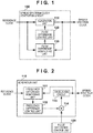
- the spread spectrum clock generation circuit 100 generates a spread spectrum clock based on an externally input reference clock, and outputs the spread spectrum clock to the outside.
- a reference clock may be a clock whose frequency is constant over time.
- a spread spectrum clock is a clock obtained by performing spread spectrum for a reference clock, and varies in frequency over time.
- the spread spectrum clock generation circuit 100 includes a generation unit 110, a pulse difference control unit 120, and a pulse difference monitoring unit 130.
- the reference clock input to the spread spectrum clock generation circuit 100 is supplied to the generation unit 110 and the pulse difference monitoring unit 130.
- the generation unit 110 generates a spread spectrum clock based on the supplied reference clock.
- the generation unit 110 outputs the generated spread spectrum clock to the outside, and supplies the clock to the pulse difference monitoring unit 130.
- the generation unit 110 may generate a spread spectrum clock so as to match the average frequency of the reference clock with that of the spread spectrum clock to be output.
- the pulse difference monitoring unit 130 continuously monitors the difference between the number of pulses of the reference clock input to the generation unit 110 after a given time and the number of pulses of the spread spectrum clock output from the generation unit 110 after the same time.
- this start time is called a reference time
- the difference between the numbers of pulses of the two clocks is called a pulse difference.
- a pulse difference may be defined as the value obtained by subtracting the number of pulses of a spread spectrum clock from that of a reference clock.
- a pulse difference may be defined as the value obtained by subtracting the number of pulses of a reference clock from that of a spread spectrum clock.
- the pulse difference monitoring unit 130 supplies a signal representing the pulse difference to the pulse difference control unit 120.
- the pulse difference control unit 120 controls the generation unit 110 to adjust the frequency of the spread spectrum clock output from the generation unit 110 so as to make the pulse difference fall within a predetermined range. The operation of the pulse difference control unit 120 will be described in detail later.
- the generation unit 110 may include a frequency difference monitoring unit 111, a frequency difference control unit 112, an oscillation circuit 113, and an adder 114.
- the frequency difference monitoring unit 111 continuously monitors the difference between the average frequency of the reference clock input to the generation unit 110 and the average frequency of the spread spectrum clock output from the generation unit 110. The difference between average frequencies will be simply referred to as the average frequency difference hereinafter.
- the frequency difference monitoring unit 111 supplies a signal representing the average frequency difference to the frequency difference control unit 112.
- the frequency difference control unit 112 supplies, to the adder 114, a signal which makes the oscillation frequency of the oscillation circuit 113 vary within a predetermined range at a predetermined period.
- the adder 114 adds the signal supplied from the frequency difference control unit 112 to the signal supplied from the pulse difference control unit 120 and supplies the resultant signal to the oscillation circuit 113. If no significant signal is supplied from the pulse difference control unit 120 to the adder 114, the oscillation circuit 113 operates in accordance with the signal supplied from the frequency difference control unit 112.
- the oscillation circuit 113 generates and outputs a spread spectrum clock in accordance with the signal supplied from the adder 114.
- the frequency difference control unit 112 adjusts the average frequency of the spread spectrum clock generated by the oscillation circuit 113 so as to match the average frequency with that of the reference clock, based on the average frequency difference supplied from the frequency difference monitoring unit 111.
- the frequency difference monitoring unit 111 may therefore measure an average frequency in a period in which the average frequency of a spread spectrum clock is almost constant over time when the generation unit 110 operates in a steady state without being influenced by a disturbance or the like.
- the frequency difference control unit 112 makes the frequency of a spread spectrum clock periodically vary, the period (to be referred to as the spread modulation period hereinafter) or an integer multiple of the period may be acquired as an average frequency.
- the frequency difference monitoring unit 111 may have three counters.
- the first counter counts the number of pulses of a reference clock.
- the second counter counts the number of pulses of a spread spectrum clock.
- the third counter counts the time from the instant one of these counters reaches a predetermined count value to the instant the other counter reaches the same count value.
- the frequency difference monitoring unit 111 supplies an output from the third counter as an average frequency difference to the frequency difference control unit 112.
- the frequency difference monitoring unit 111 may operate so as to tolerate these errors and variations.
- the above predetermined count value may be set to be larger than the spread modulation period of the frequency, and an output from the frequency difference control unit 112 may be changed only when the count value of the third counter exceeds a threshold. Making the frequency difference control unit 112 operate in this manner can match the average frequency of the spread spectrum clock output from the oscillation circuit 113 with the frequency of the reference clock when observation is performed with a low frequency.
- the generation unit 110 may use a PLL (Phase Locked Loop) which matches a phase of the signal obtained by dividing the reference clock with a phase of the signal obtained by dividing the spread spectrum clock.
- PLL Phase Locked Loop
- the time constant of a feedback loop may be set to be larger than a spread modulation period in order to perform frequency modulation of a spread spectrum clock in an intended manner.
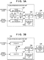
- the pulse difference monitoring unit 130 shown in Fig. 3A may include two cyclic shift registers 131 and 132, a set/reset flip-flop circuit group 133, an acquisition unit 134, and an initial value storage unit 135.
- the cyclic shift register 131 may be driven by a reference clock.
- the cyclic shift register 132 may be driven by a spread spectrum clock.
- Each of the cyclic shift registers 131 and 132 may have the number of stages equal to or more than the allowable range of pulse differences.
- each of the cyclic shift registers 131 and 132 may have the number of stages equal to or more than (Db - Da).
- Each of the cyclic shift registers 131 and 132 may have the number of stages equal to (Db - Da).
- the width ((Db - Da) in the above case) of the allowable range of pulse differences is represented by M, and each of the cyclic shift registers 131 and 132 has M stages.
- Each of the cyclic shift registers 131 and 132 outputs H (High) to only one of the M outputs, and outputs L (Low) to the remaining outputs.
- the set/reset flip-flop circuit group 133 may include M set/reset flip-flop circuits.
- the M output terminals of the cyclic shift register 131 correspond one-to-one to the M set terminals of the M set/reset flip-flop circuits.
- Each set/reset flip-flop circuit is set upon receiving H from a corresponding output terminal of the cyclic shift register 131.
- the M output terminals of the cyclic shift register 132 correspond one-to-one to the M reset terminals of the M set/reset flip-flop circuits.
- Each set/reset flip-flop circuit is reset upon receiving H from a corresponding output terminal of the cyclic shift register 132.
- the output terminals of the M set/reset flip-flop circuits are connected to the acquisition unit 134.
- Each set/reset flip-flop circuit outputs H when its internal state is a set state, and outputs L when its internal state is a reset state.
- the acquisition unit 134 counts the number of outputs, of M outputs from the set/reset flip-flop circuit group 133, which are set at H, or counts the number of outputs which are set at L. The following will exemplify a case in which the acquisition unit 134 counts the number of H outputs.
- the acquisition unit 134 stores the number of H outputs at a reference time in the initial value storage unit 135. Every time any one of M outputs from the set/reset flip-flop circuit group 133 changes, the acquisition unit 134 supplies, to the pulse difference control unit 120, the value obtained by subtracting the value stored in the initial value storage unit 135 from the number of H outputs at that time. This value represents the pulse difference.
- the pulse difference control unit 120 supplies a control signal to the generation unit 110 so as to make the pulse difference fall within a predetermined range.
- the pulse difference monitoring unit 130 shown in Fig. 3B may include two counters 136 and 137, a subtracter 138, the acquisition unit 134, and the initial value storage unit 135.
- the counter 136 counts the number of pulses of a reference clock and supplies the count value to the subtracter 138.
- the counter 137 counts the number of pulses of a spread spectrum clock and supplies the count value to the subtracter 138.
- Each of the counters 136 and 137 may count the number of pulses equal to or more than the width (M described above) of the allowable range of pulse differences.
- the subtracter 138 subtracts the count value supplied from the counter 137 from the count value supplied from the counter 136, and supplies the resultant value to the acquisition unit 134.
- the counter 137 which operates asynchronously with a reference clock, may output a count value in the form of a gray code. Outputting a count value in the form of a gray code can reduce the count value error input to the subtracter 138 to 1 or less.
- the acquisition unit 134 stores an output value from the subtracter 138 at a reference time in the initial value storage unit 135. Every time an output value from the subtracter 138 changes, the acquisition unit 134 supplies, to the pulse difference control unit 120, the value obtained by subtracting the value stored in the initial value storage unit 135 from the output value at that time. This value represents the pulse difference. Based on the pulse difference supplied from the acquisition unit 134, the pulse difference control unit 120 supplies a control signal to the generation unit 110 so as to make the pulse difference fall within a predetermined range.
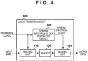
- the clock transfer circuit 400 may include the spread spectrum clock generation circuit 100, a writing unit 410, a memory 420, and a reading unit 430.
- a reference clock and input data are externally supplied to the clock transfer circuit 400.
- Input data may be, for example, N-bit digital data.
- the memory 420 can store M N-bit digital data.
- the writing unit 410 writes input data in the memory 420 upon changing storage areas one by one every time a pulse of a reference clock is input.
- the spread spectrum clock generation circuit 100 generates a spread spectrum clock based on the reference clock in the above manner, and supplies the clock to the reading unit 430.
- the reading unit 430 reads out data from the memory 420 in the FIFO (First-In First-Out) scheme every time a pulse of a spread spectrum clock is input, and outputs the clock to the outside.
- FIFO First-In First-Out
- the frequency difference control unit 112 included in the spread spectrum clock generation circuit 100 performs control to match the average frequency of a reference clock with that of a spread spectrum clock. For this reason, the number of data input to the clock transfer circuit 400 can match the number of data output from the clock transfer circuit 400 over a long period of time (for example, a length equal to or more than a spread modulation period).
- data ready to be output in the memory 420 varies when observed in a short period of time.
- data ready to be output represents data which has not been read out after being written in the memory 420.
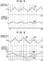
- the manner of how the number of data ready to be output in the memory 420 varies will be described with reference to Fig. 5 .
- the upper graph in Fig. 5 shows a curve 501 representing changes in the frequency of a spread spectrum clock as a function of time.
- a spread spectrum clock periodically varies up and down relative to a reference clock (Ref in Fig. 5).
- Fig. 5 shows a case on the assumption that there is no disturbance. In this case, therefore, the average frequency of a spread spectrum clock is equal to that of a reference clock.
- the lower graph in Fig. 5 shows a curve 502 representing changes in the number of data ready to be output in the memory 420 as a function of time.
- the number of data ready to be output decreases. If the frequency of a spread spectrum clock is lower than that of a reference clock, the number of data ready to be output increases. For this reason, the number of data ready to be output varies centered on a value Ini at time to.
- the manner of how the number of data ready to be output in the memory 420 varies in the presence of a disturbance will be described next with reference to Fig. 6 .
- the upper graph in Fig. 6 shows a curve 601 representing changes in the frequency of a spread spectrum clock as a function of time.
- the lower graph in Fig. 6 shows a curve 602 representing changes in the number of data ready to be output in the memory 420 as a function of time.
- a disturbance occurs at time t1
- the frequency of a generated spread spectrum clock becomes higher than the frequency which should be generated (a dotted line curve 501). For this reason, the number of data read out from the memory 420 increases.
- the number of data ready to be output becomes 0, resulting in a readout error. It is also possible to eliminate the influence of such a disturbance by the control of the frequency difference control unit 112. However, since the time constant of a feedback loop in the control of the frequency difference control unit 112 is large, it is sometimes impossible to cope with a case in which a disturbance changes faster than the time constant. If, for example, the temperature of the oscillation circuit 113 rises faster than the response time of the feedback loop due to the heat generated by a peripheral circuit of the oscillation circuit 113, the frequency generated by the oscillation circuit 113 becomes higher than the frequency which should be generated according to the temperature characteristics.
- the average frequency of a spread spectrum clock temporarily deviates from the frequency of a reference clock.
- the average frequency of a reference clock sometimes coincides with that of a spread spectrum clock depending on the timing of acquiring the average frequency. The accumulation of such errors may cause a write error and a readout error.
- the pulse difference control unit 120 adjusts the frequency of the spread spectrum clock generated by the oscillation circuit 113 so as to make a pulse difference after the reference time (after to) become equal to or more than -Ini and equal to or less than (M - Ini). If a pulse difference after reference time to falls within this range, the number of data ready to be output in the memory 420 becomes equal to or more than 1 and equal to or less than M, and no readout error or write error occurs.
- the value of Ini may be, for example, M/2.
- the pulse difference monitoring unit 130 continuously monitors pulse differences with time to at which the number of data ready to be output has become M/2 being a reference time.
- the pulse difference control unit 120 stores four thresholds Th1 to Th4. All these thresholds are included in the range in which pulse differences should be included. These thresholds may be set together with a range in which pulse differences should be included. Assume that in the following description, the four thresholds Th1 to Th4 are arranged in ascending order. In addition, the initial value Ini is located between Th2 and Th3.
- the pulse difference control unit 120 determines whether the number of data ready to be output becomes smaller than Th1 or exceeds Th4 as a result of change in pulse difference from the initial value Ini.
- the pulse difference output from the pulse difference monitoring unit 130 may change every time a pulse of a reference clock is input and a pulse of a spread spectrum clock is output. In the case shown in Fig. 6 , the pulse difference control unit 120 determines at time t2 that the pulse difference has become smaller than (Th1 - Ini), that is, the number of data ready to be output has become smaller than Th1. Since the frequency of the spread spectrum clock exhibits a decreasing tendency at time t2, the pulse difference control unit 120 continues the current operation.
- the frequency difference control unit 112 supplies a control signal to increase the frequency of the spread spectrum clock to the oscillation circuit 113.
- the pulse difference control unit 120 supplies a control signal to decrease the frequency of the spread spectrum clock to the oscillation circuit 113 so as to cancel the control of the frequency difference control unit 112.
- the frequency of the spread spectrum clock output from the oscillation circuit 113 keeps decreasing even after time t3.
- the pulse difference control unit 120 determines that the number of data ready to be output has exceeded Th2, and performs control to increase the frequency of the spread spectrum clock.
- the pulse difference control unit 120 controls the frequency of a spread spectrum clock to reduce the pulse difference so as to make the pulse difference fall within a predetermined range and, as a result, set the number of data ready to be output in the memory 420 to equal to or more than 1 and equal to or less than M.
- Such control is not limited to the above case.
- the pulse difference control unit 120 may control the frequency of a spread spectrum clock according to a predetermined time and pattern so as to make the pulse difference approach 0.
- the pulse difference control unit 120 may keep increasing/decreasing a frequency for a predetermined period so as to exceed the maximum or minimum frequency of a normal control range or may keep a frequency exceeding the maximum or minimum frequency for a predetermined period.
- the pulse difference control unit 120 may change an average frequency at the time of normal control by changing a modulation speed above and below the average frequency. In the above case, the pulse difference control unit 120 continuously changes the frequency of a spread spectrum clock. However, the pulse difference control unit 120 may discretely change the frequency.
- the spread spectrum clock generation circuit 100 can control a spread spectrum clock so as to make a pulse difference fall within a predetermined range, even if a disturbance or the like has occurred. This makes it possible to reduce the size of a memory used by the clock transfer circuit 400 by setting an allowable range of pulse differences in accordance with the size of the memory 420 which is decided in advance.
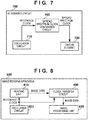
- the integrated circuit 700 may be a semiconductor integrated circuit.
- the integrated circuit 700 may include the spread spectrum clock generation circuit 100, an oscillation circuit 710, and a circuit element 720.
- the oscillation circuit 710 generates a reference clock and supplies it to the spread spectrum clock generation circuit 100.
- the spread spectrum clock generation circuit 100 generates a spread spectrum clock based on a reference clock, and supplies the spread spectrum clock to the circuit element 720.
- the circuit element 720 operates in accordance with the supplied spread spectrum clock.
- the circuit element 720 may be, for example, a flip-flop circuit.
- the image reading apparatus 800 may be, for example, an MFP (Multi Function Peripheral), scanner, or a copying machine.
- the image reading apparatus 800 may include the clock transfer circuit 400, a reading unit 810, an oscillation circuit 820, and an image processing unit 830.
- the reading unit 810 generates image data by reading a document.
- the reading unit 810 may be constituted by a light source, a reduction optical component, a line sensor, an analog/digital converter, a controller, and the like.
- the oscillation circuit 820 generates a reference clock and supplies it to the reading unit 810 and the clock transfer circuit 400.
- the reading unit 810 operates in accordance with the supplied reference clock.
- the frequency of a reference clock may be, for example, several 100 MHz.
- the clock transfer circuit 400 receives image data from the reading unit 810 in accordance with a reference clock and supplies the image data to the image processing unit 830 in accordance with a spread spectrum clock.
- the image processing unit 830 processes the supplied image data.
- the reading unit 810, the oscillation circuit 820, and the clock transfer circuit 400 may be mounted in the movable portion of the image reading apparatus 800.
- the image processing unit 830 may be mounted in the main body portion of the image reading apparatus 800.
- the clock transfer circuit 400 and the image processing unit 830 may be connected to each other via a wire harness of several ten cm.
Landscapes
- Engineering & Computer Science (AREA)
- Theoretical Computer Science (AREA)
- Physics & Mathematics (AREA)
- General Engineering & Computer Science (AREA)
- General Physics & Mathematics (AREA)
- Multimedia (AREA)
- Signal Processing (AREA)
- Electromagnetism (AREA)
- Manipulation Of Pulses (AREA)
- Image Input (AREA)
- Facsimile Heads (AREA)
- Synchronisation In Digital Transmission Systems (AREA)
- Stabilization Of Oscillater, Synchronisation, Frequency Synthesizers (AREA)
Applications Claiming Priority (1)
| Application Number | Priority Date | Filing Date | Title |
|---|---|---|---|
| JP2013169924A JP6152014B2 (ja) | 2013-08-19 | 2013-08-19 | スペクトラム拡散クロック生成回路、クロック乗せ換え回路、集積回路及び画像読み取り装置 |
Publications (2)
| Publication Number | Publication Date |
|---|---|
| EP2840778A1 EP2840778A1 (en) | 2015-02-25 |
| EP2840778B1 true EP2840778B1 (en) | 2017-02-08 |
Family
ID=51301121
Family Applications (1)
| Application Number | Title | Priority Date | Filing Date |
|---|---|---|---|
| EP14178333.2A Not-in-force EP2840778B1 (en) | 2013-08-19 | 2014-07-24 | Spread spectrum clock generation circuit, clock transfer circuit, integrated circuit, and image reading apparatus |
Country Status (4)
| Country | Link |
|---|---|
| US (1) | US9639114B2 (enExample) |
| EP (1) | EP2840778B1 (enExample) |
| JP (1) | JP6152014B2 (enExample) |
| CN (1) | CN104426504B (enExample) |
Families Citing this family (7)
| Publication number | Priority date | Publication date | Assignee | Title |
|---|---|---|---|---|
| CN105634485A (zh) * | 2015-12-22 | 2016-06-01 | 华为技术有限公司 | 扩频时钟产生装置和生成扩频时钟信号的方法 |
| US10129166B2 (en) * | 2016-06-21 | 2018-11-13 | Intel Corporation | Low latency re-timer |
| US10571953B2 (en) | 2017-07-05 | 2020-02-25 | Intel Corporation | Method and apparatus to utilize a digital-time-conversion (DTC) based clocking in computing systems |
| US12287717B2 (en) * | 2018-06-06 | 2025-04-29 | Canaan Creative Co., Ltd. | Chip frequency modulation method and apparatus of computing device, hash board, computing device and storage medium |
| US11714127B2 (en) | 2018-06-12 | 2023-08-01 | International Business Machines Corporation | On-chip spread spectrum characterization |
| US11146307B1 (en) * | 2020-04-13 | 2021-10-12 | International Business Machines Corporation | Detecting distortion in spread spectrum signals |
| US11693446B2 (en) | 2021-10-20 | 2023-07-04 | International Business Machines Corporation | On-chip spread spectrum synchronization between spread spectrum sources |
Family Cites Families (12)
| Publication number | Priority date | Publication date | Assignee | Title |
|---|---|---|---|---|
| US5488627A (en) * | 1993-11-29 | 1996-01-30 | Lexmark International, Inc. | Spread spectrum clock generator and associated method |
| JP3013033B2 (ja) * | 1997-02-13 | 2000-02-28 | 日本電気エンジニアリング株式会社 | 蓄積データ量監視回路 |
| US6294936B1 (en) * | 1998-09-28 | 2001-09-25 | American Microsystems, Inc. | Spread-spectrum modulation methods and circuit for clock generator phase-locked loop |
| JP3722403B2 (ja) * | 1999-09-22 | 2005-11-30 | 株式会社リコー | 画像読取装置 |
| JP4045454B2 (ja) * | 2005-02-04 | 2008-02-13 | セイコーエプソン株式会社 | アナログフロントエンド回路及び電子機器 |
| JP4104624B2 (ja) | 2005-11-25 | 2008-06-18 | シャープ株式会社 | 画像処理装置、画像読取装置及び画像形成装置 |
| JP2007225863A (ja) * | 2006-02-23 | 2007-09-06 | Matsushita Electric Ind Co Ltd | Emi低減制御装置 |
| TW200849806A (en) * | 2007-06-01 | 2008-12-16 | Tai 1 Microelectronics Corp | Frequency-hopping carrier generator |
| US8094698B2 (en) * | 2008-01-29 | 2012-01-10 | Realtek Semiconductor Corp. | Method for generating a spread spectrum clock and apparatus thereof |
| CN101630951B (zh) | 2008-07-14 | 2011-08-17 | 瑞鼎科技股份有限公司 | 扩频时钟信号发生器 |
| JP2010220148A (ja) * | 2009-03-19 | 2010-09-30 | Kawasaki Microelectronics Inc | コード生成回路およびイメージセンサ |
| KR101654218B1 (ko) * | 2010-01-13 | 2016-09-06 | 삼성전자주식회사 | 스프레드 스펙트럼 클럭 발생기 |
-
2013
- 2013-08-19 JP JP2013169924A patent/JP6152014B2/ja not_active Expired - Fee Related
-
2014
- 2014-07-24 EP EP14178333.2A patent/EP2840778B1/en not_active Not-in-force
- 2014-07-30 US US14/446,415 patent/US9639114B2/en not_active Expired - Fee Related
- 2014-08-14 CN CN201410398213.4A patent/CN104426504B/zh not_active Expired - Fee Related
Non-Patent Citations (1)
| Title |
|---|
| None * |
Also Published As
| Publication number | Publication date |
|---|---|
| US9639114B2 (en) | 2017-05-02 |
| US20150052379A1 (en) | 2015-02-19 |
| JP2015039148A (ja) | 2015-02-26 |
| CN104426504A (zh) | 2015-03-18 |
| CN104426504B (zh) | 2017-03-01 |
| EP2840778A1 (en) | 2015-02-25 |
| JP6152014B2 (ja) | 2017-06-21 |
Similar Documents
| Publication | Publication Date | Title |
|---|---|---|
| EP2840778B1 (en) | Spread spectrum clock generation circuit, clock transfer circuit, integrated circuit, and image reading apparatus | |
| US7242223B1 (en) | Clock frequency monitor | |
| US8164367B1 (en) | Spread spectrum clock generation technique for imaging applications | |
| US7002415B2 (en) | Frequency locked loop | |
| JP3883063B2 (ja) | クロック生成装置 | |
| JP6707503B2 (ja) | 位相ロックループにおける高速整定鋸歯状ランプ生成 | |
| US7562237B2 (en) | Semiconductor integrated circuit device with internal power control system | |
| US8160117B1 (en) | Line rate spread spectrum clock generator for use in line imaging systems | |
| US8552775B2 (en) | Digital phase-locked loop apparatus using frequency shift keying and method of controlling the same | |
| US8634446B2 (en) | Frequency level detecting method | |
| US20070079166A1 (en) | Compensated-clock generating circuit and USB device having same | |
| CN107864346B (zh) | 无参考时钟的cmos图像传感器、系统和方法 | |
| JP5257089B2 (ja) | 画像読取装置および画像形成装置 | |
| US8712709B2 (en) | Delta-sigma AD converter circuit and battery pack | |
| JP2015039148A5 (enExample) | ||
| US8135103B1 (en) | Mixed domain spread spectrum clocking for use in imaging systems for maximum imaging quality and optimized EMI performance | |
| US20180224281A1 (en) | Accelerator | |
| SE502901C2 (sv) | Digital faskomparator | |
| EP1801958A2 (en) | Harmonics related synchronization for switching regulators | |
| US6369625B1 (en) | Phase locked loop circuit | |
| JP2013219442A (ja) | 電子装置、イメージセンサおよび電子カメラ | |
| CN105323469B (zh) | 信号生成装置、有源线缆及信号生成方法 | |
| JP2004258868A (ja) | クロック発生回路 | |
| CN118805382A (zh) | 时钟控制电路以及摄像元件 | |
| JP2008090774A (ja) | スペクトラム拡散クロック発生装置 |
Legal Events
| Date | Code | Title | Description |
|---|---|---|---|
| PUAI | Public reference made under article 153(3) epc to a published international application that has entered the european phase |
Free format text: ORIGINAL CODE: 0009012 |
|
| 17P | Request for examination filed |
Effective date: 20140724 |
|
| AK | Designated contracting states |
Kind code of ref document: A1 Designated state(s): AL AT BE BG CH CY CZ DE DK EE ES FI FR GB GR HR HU IE IS IT LI LT LU LV MC MK MT NL NO PL PT RO RS SE SI SK SM TR |
|
| AX | Request for extension of the european patent |
Extension state: BA ME |
|
| R17P | Request for examination filed (corrected) |
Effective date: 20150825 |
|
| RBV | Designated contracting states (corrected) |
Designated state(s): AL AT BE BG CH CY CZ DE DK EE ES FI FR GB GR HR HU IE IS IT LI LT LU LV MC MK MT NL NO PL PT RO RS SE SI SK SM TR |
|
| 17Q | First examination report despatched |
Effective date: 20160315 |
|
| RIC1 | Information provided on ipc code assigned before grant |
Ipc: H03L 7/08 20060101ALI20160728BHEP Ipc: G06F 1/08 20060101ALI20160728BHEP Ipc: H04N 5/357 20110101AFI20160728BHEP Ipc: G06F 1/04 20060101ALI20160728BHEP Ipc: H04W 56/00 20090101ALI20160728BHEP Ipc: H04N 5/376 20110101ALI20160728BHEP |
|
| GRAP | Despatch of communication of intention to grant a patent |
Free format text: ORIGINAL CODE: EPIDOSNIGR1 |
|
| INTG | Intention to grant announced |
Effective date: 20160914 |
|
| GRAS | Grant fee paid |
Free format text: ORIGINAL CODE: EPIDOSNIGR3 |
|
| GRAA | (expected) grant |
Free format text: ORIGINAL CODE: 0009210 |
|
| AK | Designated contracting states |
Kind code of ref document: B1 Designated state(s): AL AT BE BG CH CY CZ DE DK EE ES FI FR GB GR HR HU IE IS IT LI LT LU LV MC MK MT NL NO PL PT RO RS SE SI SK SM TR |
|
| REG | Reference to a national code |
Ref country code: GB Ref legal event code: FG4D |
|
| REG | Reference to a national code |
Ref country code: CH Ref legal event code: EP Ref country code: AT Ref legal event code: REF Ref document number: 867296 Country of ref document: AT Kind code of ref document: T Effective date: 20170215 |
|
| REG | Reference to a national code |
Ref country code: IE Ref legal event code: FG4D |
|
| REG | Reference to a national code |
Ref country code: DE Ref legal event code: R096 Ref document number: 602014006689 Country of ref document: DE |
|
| REG | Reference to a national code |
Ref country code: LT Ref legal event code: MG4D |
|
| REG | Reference to a national code |
Ref country code: NL Ref legal event code: MP Effective date: 20170208 |
|
| REG | Reference to a national code |
Ref country code: AT Ref legal event code: MK05 Ref document number: 867296 Country of ref document: AT Kind code of ref document: T Effective date: 20170208 |
|
| PG25 | Lapsed in a contracting state [announced via postgrant information from national office to epo] |
Ref country code: FI Free format text: LAPSE BECAUSE OF FAILURE TO SUBMIT A TRANSLATION OF THE DESCRIPTION OR TO PAY THE FEE WITHIN THE PRESCRIBED TIME-LIMIT Effective date: 20170208 Ref country code: NO Free format text: LAPSE BECAUSE OF FAILURE TO SUBMIT A TRANSLATION OF THE DESCRIPTION OR TO PAY THE FEE WITHIN THE PRESCRIBED TIME-LIMIT Effective date: 20170508 Ref country code: GR Free format text: LAPSE BECAUSE OF FAILURE TO SUBMIT A TRANSLATION OF THE DESCRIPTION OR TO PAY THE FEE WITHIN THE PRESCRIBED TIME-LIMIT Effective date: 20170509 Ref country code: HR Free format text: LAPSE BECAUSE OF FAILURE TO SUBMIT A TRANSLATION OF THE DESCRIPTION OR TO PAY THE FEE WITHIN THE PRESCRIBED TIME-LIMIT Effective date: 20170208 Ref country code: LT Free format text: LAPSE BECAUSE OF FAILURE TO SUBMIT A TRANSLATION OF THE DESCRIPTION OR TO PAY THE FEE WITHIN THE PRESCRIBED TIME-LIMIT Effective date: 20170208 |
|
| PG25 | Lapsed in a contracting state [announced via postgrant information from national office to epo] |
Ref country code: BG Free format text: LAPSE BECAUSE OF FAILURE TO SUBMIT A TRANSLATION OF THE DESCRIPTION OR TO PAY THE FEE WITHIN THE PRESCRIBED TIME-LIMIT Effective date: 20170508 Ref country code: LV Free format text: LAPSE BECAUSE OF FAILURE TO SUBMIT A TRANSLATION OF THE DESCRIPTION OR TO PAY THE FEE WITHIN THE PRESCRIBED TIME-LIMIT Effective date: 20170208 Ref country code: PT Free format text: LAPSE BECAUSE OF FAILURE TO SUBMIT A TRANSLATION OF THE DESCRIPTION OR TO PAY THE FEE WITHIN THE PRESCRIBED TIME-LIMIT Effective date: 20170608 Ref country code: AT Free format text: LAPSE BECAUSE OF FAILURE TO SUBMIT A TRANSLATION OF THE DESCRIPTION OR TO PAY THE FEE WITHIN THE PRESCRIBED TIME-LIMIT Effective date: 20170208 Ref country code: RS Free format text: LAPSE BECAUSE OF FAILURE TO SUBMIT A TRANSLATION OF THE DESCRIPTION OR TO PAY THE FEE WITHIN THE PRESCRIBED TIME-LIMIT Effective date: 20170208 Ref country code: SE Free format text: LAPSE BECAUSE OF FAILURE TO SUBMIT A TRANSLATION OF THE DESCRIPTION OR TO PAY THE FEE WITHIN THE PRESCRIBED TIME-LIMIT Effective date: 20170208 Ref country code: ES Free format text: LAPSE BECAUSE OF FAILURE TO SUBMIT A TRANSLATION OF THE DESCRIPTION OR TO PAY THE FEE WITHIN THE PRESCRIBED TIME-LIMIT Effective date: 20170208 Ref country code: NL Free format text: LAPSE BECAUSE OF FAILURE TO SUBMIT A TRANSLATION OF THE DESCRIPTION OR TO PAY THE FEE WITHIN THE PRESCRIBED TIME-LIMIT Effective date: 20170208 |
|
| PG25 | Lapsed in a contracting state [announced via postgrant information from national office to epo] |
Ref country code: SK Free format text: LAPSE BECAUSE OF FAILURE TO SUBMIT A TRANSLATION OF THE DESCRIPTION OR TO PAY THE FEE WITHIN THE PRESCRIBED TIME-LIMIT Effective date: 20170208 Ref country code: EE Free format text: LAPSE BECAUSE OF FAILURE TO SUBMIT A TRANSLATION OF THE DESCRIPTION OR TO PAY THE FEE WITHIN THE PRESCRIBED TIME-LIMIT Effective date: 20170208 Ref country code: RO Free format text: LAPSE BECAUSE OF FAILURE TO SUBMIT A TRANSLATION OF THE DESCRIPTION OR TO PAY THE FEE WITHIN THE PRESCRIBED TIME-LIMIT Effective date: 20170208 Ref country code: IT Free format text: LAPSE BECAUSE OF FAILURE TO SUBMIT A TRANSLATION OF THE DESCRIPTION OR TO PAY THE FEE WITHIN THE PRESCRIBED TIME-LIMIT Effective date: 20170208 Ref country code: CZ Free format text: LAPSE BECAUSE OF FAILURE TO SUBMIT A TRANSLATION OF THE DESCRIPTION OR TO PAY THE FEE WITHIN THE PRESCRIBED TIME-LIMIT Effective date: 20170208 |
|
| REG | Reference to a national code |
Ref country code: DE Ref legal event code: R097 Ref document number: 602014006689 Country of ref document: DE |
|
| PG25 | Lapsed in a contracting state [announced via postgrant information from national office to epo] |
Ref country code: SM Free format text: LAPSE BECAUSE OF FAILURE TO SUBMIT A TRANSLATION OF THE DESCRIPTION OR TO PAY THE FEE WITHIN THE PRESCRIBED TIME-LIMIT Effective date: 20170208 Ref country code: PL Free format text: LAPSE BECAUSE OF FAILURE TO SUBMIT A TRANSLATION OF THE DESCRIPTION OR TO PAY THE FEE WITHIN THE PRESCRIBED TIME-LIMIT Effective date: 20170208 Ref country code: DK Free format text: LAPSE BECAUSE OF FAILURE TO SUBMIT A TRANSLATION OF THE DESCRIPTION OR TO PAY THE FEE WITHIN THE PRESCRIBED TIME-LIMIT Effective date: 20170208 |
|
| PLBE | No opposition filed within time limit |
Free format text: ORIGINAL CODE: 0009261 |
|
| STAA | Information on the status of an ep patent application or granted ep patent |
Free format text: STATUS: NO OPPOSITION FILED WITHIN TIME LIMIT |
|
| 26N | No opposition filed |
Effective date: 20171109 |
|
| PG25 | Lapsed in a contracting state [announced via postgrant information from national office to epo] |
Ref country code: SI Free format text: LAPSE BECAUSE OF FAILURE TO SUBMIT A TRANSLATION OF THE DESCRIPTION OR TO PAY THE FEE WITHIN THE PRESCRIBED TIME-LIMIT Effective date: 20170208 |
|
| REG | Reference to a national code |
Ref country code: CH Ref legal event code: PL |
|
| REG | Reference to a national code |
Ref country code: IE Ref legal event code: MM4A |
|
| REG | Reference to a national code |
Ref country code: FR Ref legal event code: ST Effective date: 20180330 |
|
| PG25 | Lapsed in a contracting state [announced via postgrant information from national office to epo] |
Ref country code: LI Free format text: LAPSE BECAUSE OF NON-PAYMENT OF DUE FEES Effective date: 20170731 Ref country code: IE Free format text: LAPSE BECAUSE OF NON-PAYMENT OF DUE FEES Effective date: 20170724 Ref country code: CH Free format text: LAPSE BECAUSE OF NON-PAYMENT OF DUE FEES Effective date: 20170731 |
|
| PG25 | Lapsed in a contracting state [announced via postgrant information from national office to epo] |
Ref country code: FR Free format text: LAPSE BECAUSE OF NON-PAYMENT OF DUE FEES Effective date: 20170731 |
|
| REG | Reference to a national code |
Ref country code: BE Ref legal event code: MM Effective date: 20170731 |
|
| PG25 | Lapsed in a contracting state [announced via postgrant information from national office to epo] |
Ref country code: LU Free format text: LAPSE BECAUSE OF NON-PAYMENT OF DUE FEES Effective date: 20170724 |
|
| PG25 | Lapsed in a contracting state [announced via postgrant information from national office to epo] |
Ref country code: BE Free format text: LAPSE BECAUSE OF NON-PAYMENT OF DUE FEES Effective date: 20170731 |
|
| PG25 | Lapsed in a contracting state [announced via postgrant information from national office to epo] |
Ref country code: MT Free format text: LAPSE BECAUSE OF NON-PAYMENT OF DUE FEES Effective date: 20170724 |
|
| GBPC | Gb: european patent ceased through non-payment of renewal fee |
Effective date: 20180724 |
|
| PG25 | Lapsed in a contracting state [announced via postgrant information from national office to epo] |
Ref country code: GB Free format text: LAPSE BECAUSE OF NON-PAYMENT OF DUE FEES Effective date: 20180724 |
|
| PG25 | Lapsed in a contracting state [announced via postgrant information from national office to epo] |
Ref country code: HU Free format text: LAPSE BECAUSE OF FAILURE TO SUBMIT A TRANSLATION OF THE DESCRIPTION OR TO PAY THE FEE WITHIN THE PRESCRIBED TIME-LIMIT; INVALID AB INITIO Effective date: 20140724 Ref country code: MC Free format text: LAPSE BECAUSE OF FAILURE TO SUBMIT A TRANSLATION OF THE DESCRIPTION OR TO PAY THE FEE WITHIN THE PRESCRIBED TIME-LIMIT Effective date: 20170208 |
|
| PG25 | Lapsed in a contracting state [announced via postgrant information from national office to epo] |
Ref country code: CY Free format text: LAPSE BECAUSE OF FAILURE TO SUBMIT A TRANSLATION OF THE DESCRIPTION OR TO PAY THE FEE WITHIN THE PRESCRIBED TIME-LIMIT Effective date: 20170208 |
|
| PG25 | Lapsed in a contracting state [announced via postgrant information from national office to epo] |
Ref country code: MK Free format text: LAPSE BECAUSE OF FAILURE TO SUBMIT A TRANSLATION OF THE DESCRIPTION OR TO PAY THE FEE WITHIN THE PRESCRIBED TIME-LIMIT Effective date: 20170208 |
|
| PG25 | Lapsed in a contracting state [announced via postgrant information from national office to epo] |
Ref country code: TR Free format text: LAPSE BECAUSE OF FAILURE TO SUBMIT A TRANSLATION OF THE DESCRIPTION OR TO PAY THE FEE WITHIN THE PRESCRIBED TIME-LIMIT Effective date: 20170208 |
|
| PG25 | Lapsed in a contracting state [announced via postgrant information from national office to epo] |
Ref country code: AL Free format text: LAPSE BECAUSE OF FAILURE TO SUBMIT A TRANSLATION OF THE DESCRIPTION OR TO PAY THE FEE WITHIN THE PRESCRIBED TIME-LIMIT Effective date: 20170208 Ref country code: IS Free format text: LAPSE BECAUSE OF FAILURE TO SUBMIT A TRANSLATION OF THE DESCRIPTION OR TO PAY THE FEE WITHIN THE PRESCRIBED TIME-LIMIT Effective date: 20170608 |
|
| REG | Reference to a national code |
Ref country code: DE Ref legal event code: R079 Ref document number: 602014006689 Country of ref document: DE Free format text: PREVIOUS MAIN CLASS: H04N0005357000 Ipc: H04N0025600000 |
|
| PGFP | Annual fee paid to national office [announced via postgrant information from national office to epo] |
Ref country code: DE Payment date: 20230620 Year of fee payment: 10 |
|
| REG | Reference to a national code |
Ref country code: DE Ref legal event code: R119 Ref document number: 602014006689 Country of ref document: DE |
|
| PG25 | Lapsed in a contracting state [announced via postgrant information from national office to epo] |
Ref country code: DE Free format text: LAPSE BECAUSE OF NON-PAYMENT OF DUE FEES Effective date: 20250201 |