EP2833388B1 - MEMS-Schaltervorrichtung und Herstellungsverfahren - Google Patents
MEMS-Schaltervorrichtung und Herstellungsverfahren Download PDFInfo
- Publication number
- EP2833388B1 EP2833388B1 EP14178181.5A EP14178181A EP2833388B1 EP 2833388 B1 EP2833388 B1 EP 2833388B1 EP 14178181 A EP14178181 A EP 14178181A EP 2833388 B1 EP2833388 B1 EP 2833388B1
- Authority
- EP
- European Patent Office
- Prior art keywords
- mems switch
- insulating layer
- mems
- switch device
- conductive
- Prior art date
- Legal status (The legal status is an assumption and is not a legal conclusion. Google has not performed a legal analysis and makes no representation as to the accuracy of the status listed.)
- Active
Links
Images



Classifications
-
- H—ELECTRICITY
- H01—ELECTRIC ELEMENTS
- H01H—ELECTRIC SWITCHES; RELAYS; SELECTORS; EMERGENCY PROTECTIVE DEVICES
- H01H59/00—Electrostatic relays; Electro-adhesion relays
- H01H59/0009—Electrostatic relays; Electro-adhesion relays making use of micromechanics
-
- B—PERFORMING OPERATIONS; TRANSPORTING
- B81—MICROSTRUCTURAL TECHNOLOGY
- B81B—MICROSTRUCTURAL DEVICES OR SYSTEMS, e.g. MICROMECHANICAL DEVICES
- B81B7/00—Microstructural systems ; Auxiliary parts of microstructural devices or systems
- B81B7/0032—Packages or encapsulation
- B81B7/007—Interconnections between the MEMS and external electrical signals
-
- B—PERFORMING OPERATIONS; TRANSPORTING
- B81—MICROSTRUCTURAL TECHNOLOGY
- B81C—PROCESSES OR APPARATUS SPECIALLY ADAPTED FOR THE MANUFACTURE OR TREATMENT OF MICROSTRUCTURAL DEVICES OR SYSTEMS
- B81C1/00—Manufacture or treatment of devices or systems in or on a substrate
- B81C1/00015—Manufacture or treatment of devices or systems in or on a substrate for manufacturing microsystems
- B81C1/00341—Processes for manufacturing microsystems not provided for in groups B81C1/00023 - B81C1/00261
-
- B—PERFORMING OPERATIONS; TRANSPORTING
- B81—MICROSTRUCTURAL TECHNOLOGY
- B81B—MICROSTRUCTURAL DEVICES OR SYSTEMS, e.g. MICROMECHANICAL DEVICES
- B81B2201/00—Specific applications of microelectromechanical systems
- B81B2201/01—Switches
- B81B2201/012—Switches characterised by the shape
- B81B2201/014—Switches characterised by the shape having a cantilever fixed on one side connected to one or more dimples
-
- B—PERFORMING OPERATIONS; TRANSPORTING
- B81—MICROSTRUCTURAL TECHNOLOGY
- B81B—MICROSTRUCTURAL DEVICES OR SYSTEMS, e.g. MICROMECHANICAL DEVICES
- B81B2207/00—Microstructural systems or auxiliary parts thereof
- B81B2207/09—Packages
- B81B2207/091—Arrangements for connecting external electrical signals to mechanical structures inside the package
- B81B2207/092—Buried interconnects in the substrate or in the lid
-
- H—ELECTRICITY
- H01—ELECTRIC ELEMENTS
- H01H—ELECTRIC SWITCHES; RELAYS; SELECTORS; EMERGENCY PROTECTIVE DEVICES
- H01H1/00—Contacts
- H01H1/0036—Switches making use of microelectromechanical systems [MEMS]
- H01H2001/0052—Special contact materials used for MEMS
-
- H—ELECTRICITY
- H10—SEMICONDUCTOR DEVICES; ELECTRIC SOLID-STATE DEVICES NOT OTHERWISE PROVIDED FOR
- H10W—GENERIC PACKAGES, INTERCONNECTIONS, CONNECTORS OR OTHER CONSTRUCTIONAL DETAILS OF DEVICES COVERED BY CLASS H10
- H10W72/00—Interconnections or connectors in packages
- H10W72/071—Connecting or disconnecting
- H10W72/075—Connecting or disconnecting of bond wires
- H10W72/07551—Connecting or disconnecting of bond wires characterised by changes in properties of the bond wires during the connecting
- H10W72/07554—Connecting or disconnecting of bond wires characterised by changes in properties of the bond wires during the connecting changes in dispositions
-
- H—ELECTRICITY
- H10—SEMICONDUCTOR DEVICES; ELECTRIC SOLID-STATE DEVICES NOT OTHERWISE PROVIDED FOR
- H10W—GENERIC PACKAGES, INTERCONNECTIONS, CONNECTORS OR OTHER CONSTRUCTIONAL DETAILS OF DEVICES COVERED BY CLASS H10
- H10W72/00—Interconnections or connectors in packages
- H10W72/50—Bond wires
- H10W72/541—Dispositions of bond wires
- H10W72/547—Dispositions of multiple bond wires
-
- H—ELECTRICITY
- H10—SEMICONDUCTOR DEVICES; ELECTRIC SOLID-STATE DEVICES NOT OTHERWISE PROVIDED FOR
- H10W—GENERIC PACKAGES, INTERCONNECTIONS, CONNECTORS OR OTHER CONSTRUCTIONAL DETAILS OF DEVICES COVERED BY CLASS H10
- H10W72/00—Interconnections or connectors in packages
- H10W72/50—Bond wires
- H10W72/551—Materials of bond wires
- H10W72/552—Materials of bond wires comprising metals or metalloids, e.g. silver
- H10W72/5522—Materials of bond wires comprising metals or metalloids, e.g. silver comprising gold [Au]
-
- H—ELECTRICITY
- H10—SEMICONDUCTOR DEVICES; ELECTRIC SOLID-STATE DEVICES NOT OTHERWISE PROVIDED FOR
- H10W—GENERIC PACKAGES, INTERCONNECTIONS, CONNECTORS OR OTHER CONSTRUCTIONAL DETAILS OF DEVICES COVERED BY CLASS H10
- H10W74/00—Encapsulations, e.g. protective coatings
-
- H—ELECTRICITY
- H10—SEMICONDUCTOR DEVICES; ELECTRIC SOLID-STATE DEVICES NOT OTHERWISE PROVIDED FOR
- H10W—GENERIC PACKAGES, INTERCONNECTIONS, CONNECTORS OR OTHER CONSTRUCTIONAL DETAILS OF DEVICES COVERED BY CLASS H10
- H10W90/00—Package configurations
- H10W90/701—Package configurations characterised by the relative positions of pads or connectors relative to package parts
- H10W90/751—Package configurations characterised by the relative positions of pads or connectors relative to package parts of bond wires
- H10W90/753—Package configurations characterised by the relative positions of pads or connectors relative to package parts of bond wires between laterally-adjacent chips
-
- H—ELECTRICITY
- H10—SEMICONDUCTOR DEVICES; ELECTRIC SOLID-STATE DEVICES NOT OTHERWISE PROVIDED FOR
- H10W—GENERIC PACKAGES, INTERCONNECTIONS, CONNECTORS OR OTHER CONSTRUCTIONAL DETAILS OF DEVICES COVERED BY CLASS H10
- H10W90/00—Package configurations
- H10W90/701—Package configurations characterised by the relative positions of pads or connectors relative to package parts
- H10W90/751—Package configurations characterised by the relative positions of pads or connectors relative to package parts of bond wires
- H10W90/756—Package configurations characterised by the relative positions of pads or connectors relative to package parts of bond wires between a chip and a stacked lead frame, conducting package substrate or heat sink
Definitions
- Patent Publication No. WO2010072431A1 describes structures having a hybrid MEMS RF switch and a method of fabricating such structures using existing wiring layers of a device.
- Patent Publication No. WO2013033613A2 generally relates to an architecture for isolating an RF MEMS device from a substrate and driving circuit, series and shunt DVC die architectures, and smaller MEMS arrays for high frequency communications.
- Patent Publication No. US2013075888A1 describes a semiconductor package of reduced size and a method of fabricating the same.
- Patent Publication No. WO03041133A2 describes an Electrothermal Self-Latching MEMS Switch.
- a microscale switch having a movable microcomponent is provided and includes a substrate having a stationary contact.
- At least one of the conductive pathways may include a track of resistive material, such as polysilicon, the conductive pathway preferably being configured as a resistive circuit element.
- the MEMS switch module may include a switch beam, wherein the resistive circuit element is preferably formed within the insulating layer and is aligned with the switch beam.
- the substrate layer can comprise a high resistivity material, for example silicon, quartz, sapphire, gallium arsenide or glass.
- the method may further include providing a control module arranged to be in electrical communication with the MEMS switch module.
- the MEMS switch device may be encapsulated with a protective plastic material.
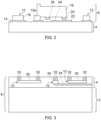
- FIG. 2 schematically illustrates the MEMS switch module 6 formed on the surface of the insulating layer 4.
- the conductive pathways 10 illustrated in Figure 1 are not illustrated for the purposes of clarity.
- the illustrated MEMS switch module 6 includes a number of electrical contacts 12 formed on the surface of the insulating layer 4.
- each contact 12 includes a first layer 14 of electrically conductive material, such as any one of the noble metals, e.g. ruthenium or platinum, formed on the surface of the insulating layer 4, and a second electrically conductive layer 16 can be formed over the top of the first layer 14.
- the second layer 16 can be more electrically conductive than the first layer 14.
- the second conductive layer 16 may be, for example, gold, which is highly conductive and highly resistant to corrosion.
- the first layer 14 can act to ensure a better electrical and physical contact with the insulating layer 4 than would be provided with a contact 12 formed solely of the second conductive material 16, such as gold.
- the MEMS switch module 6 also includes a MEMS switch beam 18 that is electrically and physically connected to a further contact 12a, which is referred to herein as an anchor contact.
- the MEMS switch beam 18 can be formed of gold in some embodiments.
- the anchor contact 12a serves a dual purpose of physically supporting one end of the switch beam 18 on the surface of the insulating layer 4 and also providing an electrical connection to the switch beam 18 via the contact 12a.
- the switch beam 18 is cantilevered from anchor contact 12a so as to be separated from the surface of the insulating layer 4.
- a contact tip 20 is formed on the underside of the beam 18, the contact tip 20 being coated in a hard conductive material, such as one of the noble metals.
- the contact tip 20 is located above a further contact pad 22, which may also be formed from a relatively hardwearing conductive material such as a noble metal.
- the provision of the hardwearing coatings 20, 22 on the contact tip 20 of the switch beam 18 and the corresponding contact pad 22 on the surface of the insulating layer 4 can prevent these surfaces from potentially softening and sticking together at high switching frequencies, which may occur if a softer conductive material, such as gold, were to be used. While not separately called out in Figures 1 and 4 , the material choices for the MEMS switch module 6 of Figure 2 are also applicable to the MEMS switch modules of Figures 1 and 4 .
- a voltage is applied to a gate electrode 24, which can also be formed from a noble metal, such as ruthenium. Applying the voltage to the gate electrode 24 creates an electrostatic force attracting the switch beam 18 towards the gate electrode 24. The electrostatic force causes the switch beam 18 to deform and the beam tip 20 to come into contact with contact pad 22, thus closing an electric circuit between the contact pad 22 and anchor contact 12a.
- a further projection or protrusion 26 is formed on the underside of the switch beam 18 between the anchor pad 12a and the gate electrode 24.
- the protrusion 26, also referred to as a "bumper” prevents the switch beam 18 from collapsing into contact with the gate electrode 24, which may occur through metal fatigue or if an excessive electrostatic force is generated.
- Figure 3 schematically illustrates the CMOS backend 8, including the substrate layer 2 and the insulating layer 4.
- the insulating layer 4 is formed from silicon dioxide, but other insulating materials known to be used instead of silicon dioxide may be used as appropriate.
- Formed within the insulating layer 4 are a number of conductive pathways 10.
- the conductive pathways include a linear trace 30 formed of a resistant material, such as aluminum, formed horizontally within the insulating layer 4.
- the conductive traces 30 can be buried within the insulating layer 4.
- a number of conductive vias 32 can extend from the traces 30 to the surface of the insulating layer 4.
- the conductive vias 32 may be formed from tungsten plugs, or other appropriate conductive material.
- the vias 32 may vary in size and number as appropriate.
- the vias 32 and traces 30 are formed within the insulating layer 4 using known bulk processing techniques, such as those typically used in the production of CMOS devices.
- the insulating substrate layer 2 is, typically, in preferred embodiments, formed from high resistivity silicon, but may be formed from other high resistivity substances, such as quartz, sapphire, gallium arsenide and glass etc.
- Other conductive pathways may be formed within the insulating layer 4, as required by the desired electrical circuitry for the MEMS switch module 6.
- An example of such a further conductive pathway is a higher resistance resistor 34, which in some embodiments is formed from high resistance poly-silicon embedded within the insulating layer 4.
- Such a resistor when formed underneath the switch beam 18 of the switch module 6 can serve the purpose of decoupling any undesirable capacitance between the switch beam 18 and the insulating layer 4.
- the conductive vias 32 form electrical interconnections between the contact pads of the MEMS switch module 6 and the conductor traces 30, thus forming the desired conductive pathways between the different elements of the MEMS switch module 6.
- the conductive pathways of the illustrated embodiment are thus completely buried within the insulating layer 4 and thus protected from corrosion and other degradation.
- a protective silicon cap 40 is placed over the switch beam 18 of the switch module 6, leaving the relevant contact pads 12 outside the protective cap 40.
- the protective cap 40 can be formed from a single block of appropriate material, i.e. silicon, with an internal cavity 42 etched out.
- the cap 40 is bonded to the surface of the insulating layer 4 on which the MEMS switch module 6 is formed using anodic bonding or using an appropriate adhesive, i.e. the illustrated glass 44.
- the protective cap 40 helps to prevent moisture and other contaminants from interfering with the switch module operation and helps prevent subsequent plastic molding steps from damaging the switch module during the plastic package assembly process.
- the protective cap 40 can also prevent mechanical damage of the MEMS switch module and can prevent particles getting underneath the switch beam 18.
- a further benefit of the protective cap 40 is to provide a controlled environment in which the actual MEMS switch operates.
- the interior cavity 42 of the cap 40 may be filled with an inert gas.
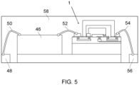
- FIG. 5 schematically illustrates the MEMS switch device and protective cap shown in Figure 4 packaged in combination with a control module 46.
- the control module 46 is preferably an application specific integrated circuit (ASIC) and is provided to generate appropriate high voltage (for example, about 80V) switching signals to be applied to the MEMS switch device in response to received logic signals, for example, about 3V.
- the lower voltage control logic signals are applied to the control module 46 by means of an input connection 48 and a wire bond connection 50 to the control module.
- a further wire bond 52 can connect an output of the control module 46 and one of the contact pads of the MEMS switch device.
- the output signals from the MEMS switch device can be output via a further wire bond 54 to an output 56 of the package.
- the input connection 48, control module 46, MEMS switch device 1 and output 56 are encapsulated in a typical packaging plastic material 58 in accordance with known packaging techniques. Whilst illustrated with the control module 46 and MEMS switch device package 1 side-by-side, alternatively the MEMS switch device 1 may be stacked on top of the control module 46, and some or all of the wirebonds can be replaced with other forms of interconnection (e.g., flipchip, through silicon vias, etc.).
- FIG. 6 is a flowchart illustrating a method for manufacturing a MEMS switch device, according to one embodiment.
- the substrate layer 2 of the CMOS backend is formed using conventional bulk processing/wafer processing techniques.
- the next step 62 is to form the insulating layer 4 over the substrate 2, with the subsequent step 64 being to form the conductive pathways in the insulating layer.
- the skilled artisan will appreciate that, in practice, portions of the insulating layer 4 are formed before and after forming the conductive pathways.
- the initial steps used to form the backend, including the conductive pathways, can all be completed using conventional bulk processing technology.
- the backend wafer is then processed in accordance with surface processing techniques to form, at step 66, the MEMS switch module on the surface of the insulating layer 4.
- the protective cap may subsequently be formed over the switch module (at step 68), with the MEMS switch device and control module, if desired, subsequently packaged in accordance with conventional packaging techniques (step 70).
- the MEMS switch device and method of fabricating the MEMS switch device according to the embodiments disclosed herein buries the conductive pathways (interconnects) in a manufacturable manner, using backend CMOS-type processing. This avoids the problems experienced with MEMS switch devices fabricated solely with surface micro-machine technology in which the interconnects were unburied and therefore were prone to corrosion and leakage currents between interconnects developing due to exposure.
- the MEMS switch beam 18 can be formed of a highly conductive and corrosion-resistant metal, particularly gold. Using gold for the switch beam 18 and the second conductive layer 16 can greatly reduce the amount of losses as compared to switches manufactured using a semiconductor material (e.g., silicon). Without being limited by theory, it is believed that a gold switch is advantageous compared to using a semiconductor switch because, when the gold switch is closed, the switch acts as a substantially loss-less analog device such that the input signal is substantially the same as the output signal (e.g., the gold switch in the closed configuration may act as a gold wire).
- the MEMS switches described herein are integrated with high frequency circuits, such as RF arrays.
- gold switch beams may be used in RF applications at operating frequencies between about 11 GHz and about 100 GHz.
- the disclosed switch beams may be used in RF applications at operating frequencies of at least about 77 GHz.
- MEMS switches as described herein are used to replace much larger mechanical relays in applications where a smaller profile is desired.
- highly reliable and loss-less MEMS switches disclosed herein may be made to be smaller than conventional mechanical relays.
- CMOS switch with conductive parts including gold, platinum, and/or ruthenium.
- CMOS backend 8 a MEMS switch module 6 that uses a gold switch beam 18
- gold used to form the switch beam 18 may contaminate the carefully calibrated CMOS facilities and any future CMOS processes used in the facility.
Landscapes
- Engineering & Computer Science (AREA)
- Microelectronics & Electronic Packaging (AREA)
- Manufacturing & Machinery (AREA)
- Computer Hardware Design (AREA)
- Micromachines (AREA)
- Contacts (AREA)
Claims (13)
- Schaltvorrichtung (1) für mikroelektromechanische Systeme (MEMS), die Folgendes enthält:eine Substratschicht (2);eine Isolierschicht (4), die über der Substratschicht gebildet ist und eine Anzahl von Leiterbahnen (10) aus Nicht-Edelmetallen, die unter Verwendung von Volumenhalbleiter-Verarbeitungstechniken in der Isolierschicht vergraben sind, enthält;ein MEMS-Schaltmodul (6), das einen Schaltträger (18) enthält und mehrere Kontakte (12) aufweist, die unter Verwendung von Oberflächen-Verarbeitungstechniken auf einer Oberfläche der Isolierschicht gebildet sind, wobei die Kontakte aus Edelmetallen gebildet sind, wobei die mehreren Kontakte (12) eine Gate-Elektrode (24) enthalten, die auf der Oberfläche der Isolierschicht (4) unter dem Schaltträger gebildet ist, und wobei die Leiterbahnen konfiguriert sind, ausgewählte Kontakte (12) des MEMS-Schaltmoduls (6) miteinander zu verbinden; undeine Schutzkappe (40) aus Silizium, die das MEMS-Schaltmodul (16) umschließt, wobei die Schutzkappe aus Silizium durch anodisches Bonden oder mittels Glas (44) als Haftmittel mit der Isolierschicht (4) verbunden ist; wobeidie Substratschicht und die Isolierschicht ein CMOS-Backend sind, das unter Verwendung einer Backend-CMOS-Typ-Verarbeitung gebildet ist.
- MEMS-Schaltvorrichtung nach Anspruch 1, wobei mindestens eine der Leiterbahnen (10) unterhalb der Oberfläche der Isolierschicht (4) einen Pfad aus leitendem Material (30) und mindestens eine leitende Durchkontaktierung (32), die sich von dem Pfad zu der Oberfläche der Isolierschicht erstreckt, enthält.
- MEMS-Schaltvorrichtung nach Anspruch 2, wobei einer oder mehrere der folgenden Punkte zutreffen:jede leitende Durchkontaktierung (32) ist mit einem der Kontakte (12) des MEMS-Schaltmoduls elektrisch verbunden;der Pfad des leitenden Materials (30) enthält Aluminium; unddie leitende Durchkontaktierung (3) enthält Wolfram.
- MEMS-Schaltvorrichtung nach einem vorhergehenden Anspruch, wobei mindestens eine der Leiterbahnen (10) einen Pfad aus resistivem Material enthält, wobei das resistive Material wahlweise Polysilizium umfasst.
- MEMS-Schaltvorrichtung nach Anspruch 4, wobei die Leiterbahn (10) als ein resistives Schaltungselement konfiguriert ist.
- MEMS-Schaltvorrichtung nach Anspruch 5, wobei das resistive Schaltungselement in der Isolierschicht (4) gebildet ist und auf den Schaltträger (18) ausgerichtet ist.
- MEMS-Schaltvorrichtung nach einem vorhergehenden Anspruch, wobei die Isolierschicht (4) Siliziumdioxid umfasst.
- MEMS-Schaltvorrichtung nach einem vorhergehenden Anspruch, die ferner ein Steuermodul (46) umfasst, das sich in elektrischer Kommunikation mit dem MEMS-Schaltmodul (6) befindet.
- MEMS-Schaltvorrichtung nach Anspruch 1, wobei die Substratschicht (2) ein Material mit hohem spezifischen Widerstand umfasst, wobei das Material mit hohem spezifischen Widerstand wahlweise eines von Silizium, Quarz, Saphir, Galliumarsenid und Glas umfasst.
- MEMS-Schaltvorrichtung nach Anspruch 1, wobei das MEMS-Schaltmodul einen MEMS-Schaltträger (18) umfasst, wobei der MEMS-Schaltträger Gold umfasst.
- Verfahren zum Herstellen einer Schaltvorrichtung (1) für mikroelektromechanische Systeme (MEMS), das Folgendes umfasst:Bilden eines CMOS-Backend durch Bilden einer Isolierschicht (4) über einer Substratschicht (2) unter Verwendung von Backend-CMOS-Typ-Verarbeitung;Bilden einer Zahl von Leiterbahnen (10) in der Isolierschicht aus Nicht-Edelmetallen und unter Verwendung von Volumenhalbleiter-Verarbeitungstechniken; undanschließend Bilden eines MEMS-Schaltmoduls (6) auf der Oberfläche der Isolierschicht (4) unter Verwendung von Oberflächen-Verarbeitungstechniken, wobei das MEMS-Schaltmodul einen Schaltträger (18) und mehrere Kontakte enthält, wobei die Kontakte aus Edelmetallen gebildet werden, wobei die mehreren Kontakte eine Gate-Elektrode (24) enthalten, die auf der Oberfläche der Isolierschicht (4) unter dem Schaltträger gebildet werden, und wobei ausgewählte Kontakte (12) konfiguriert sind, durch die Leiterbahnen (10) in der Isolierschicht miteinander verbunden zu sein; undnach dem Bilden des MEMS-Schaltmoduls (6), Bilden einer Schutzkappe (40) aus Silizium, die das MEMS-Schaltmodul umschließt, wobei die Schutzkappe aus Silizium durch anodisches Bonden oder mittels Glas (44) als Haftmittel mit der Isolierschicht verbunden wird.
- Verfahren nach Anspruch 11, das ferner das Bereitstellen eines Steuermoduls (46) enthält, das derart angeordnet ist, dass es sich in elektrischer Kommunikation mit dem MEMS-Schaltmodul (16) befindet.
- Verfahren nach Anspruch 12, das ferner das Umschließen der MEMS-Schaltvorrichtung mit einem Schutzmaterial (40) aus Kunststoff enthält.
Applications Claiming Priority (1)
| Application Number | Priority Date | Filing Date | Title |
|---|---|---|---|
| US13/955,866 US9911563B2 (en) | 2013-07-31 | 2013-07-31 | MEMS switch device and method of fabrication |
Publications (3)
| Publication Number | Publication Date |
|---|---|
| EP2833388A2 EP2833388A2 (de) | 2015-02-04 |
| EP2833388A3 EP2833388A3 (de) | 2015-03-11 |
| EP2833388B1 true EP2833388B1 (de) | 2023-12-13 |
Family
ID=51211702
Family Applications (1)
| Application Number | Title | Priority Date | Filing Date |
|---|---|---|---|
| EP14178181.5A Active EP2833388B1 (de) | 2013-07-31 | 2014-07-23 | MEMS-Schaltervorrichtung und Herstellungsverfahren |
Country Status (4)
| Country | Link |
|---|---|
| US (1) | US9911563B2 (de) |
| EP (1) | EP2833388B1 (de) |
| CN (1) | CN104347320B (de) |
| TW (1) | TWI643231B (de) |
Families Citing this family (9)
| Publication number | Priority date | Publication date | Assignee | Title |
|---|---|---|---|---|
| CN105575734B (zh) * | 2015-12-23 | 2018-11-06 | 北京时代民芯科技有限公司 | 一种射频mems开关及其制造方法 |
| CN105621351B (zh) * | 2015-12-24 | 2017-11-07 | 中国电子科技集团公司第五十五研究所 | 一种rf mems开关的圆片级封装方法 |
| US10529518B2 (en) | 2016-09-19 | 2020-01-07 | Analog Devices Global | Protection schemes for MEMS switch devices |
| FI20185058A1 (en) * | 2018-01-22 | 2019-07-23 | Tikitin Oy | Packaged microelectronic component and method for its manufacture |
| US11501928B2 (en) | 2020-03-27 | 2022-11-15 | Menlo Microsystems, Inc. | MEMS device built on substrate with ruthenium based contact surface material |
| US12202723B2 (en) | 2021-05-18 | 2025-01-21 | Analog Devices International Unlimited Company | Microelectromechanical systems (MEMS) switch and related methods |
| CN117396994A (zh) | 2021-05-18 | 2024-01-12 | 亚德诺半导体国际无限责任公司 | Mems开关的有源电荷泄放方法 |
| DE102021212369A1 (de) | 2021-11-03 | 2023-05-04 | Robert Bosch Gesellschaft mit beschränkter Haftung | Relais und Verfahren zum Betreiben eines Relais |
| CN117615987A (zh) | 2022-03-31 | 2024-02-27 | 京东方科技集团股份有限公司 | 电子器件及制备方法 |
Citations (1)
| Publication number | Priority date | Publication date | Assignee | Title |
|---|---|---|---|---|
| US20110049649A1 (en) * | 2009-08-27 | 2011-03-03 | International Business Machines Corporation | Integrated circuit switches, design structure and methods of fabricating the same |
Family Cites Families (32)
| Publication number | Priority date | Publication date | Assignee | Title |
|---|---|---|---|---|
| US5638946A (en) * | 1996-01-11 | 1997-06-17 | Northeastern University | Micromechanical switch with insulated switch contact |
| US6046659A (en) * | 1998-05-15 | 2000-04-04 | Hughes Electronics Corporation | Design and fabrication of broadband surface-micromachined micro-electro-mechanical switches for microwave and millimeter-wave applications |
| US6384353B1 (en) * | 2000-02-01 | 2002-05-07 | Motorola, Inc. | Micro-electromechanical system device |
| US6621390B2 (en) | 2001-02-28 | 2003-09-16 | Samsung Electronics Co., Ltd. | Electrostatically-actuated capacitive MEMS (micro electro mechanical system) switch |
| AU2002359370A1 (en) | 2001-11-09 | 2003-05-26 | Coventor, Incorporated | Mems device having contact and standoff bumps and related methods |
| US6624003B1 (en) * | 2002-02-06 | 2003-09-23 | Teravicta Technologies, Inc. | Integrated MEMS device and package |
| GB0206509D0 (en) * | 2002-03-20 | 2002-05-01 | Qinetiq Ltd | Micro-Electromechanical systems |
| JP2004006664A (ja) | 2002-04-10 | 2004-01-08 | Sanken Electric Co Ltd | 半導体素子の製造方法 |
| US6686820B1 (en) * | 2002-07-11 | 2004-02-03 | Intel Corporation | Microelectromechanical (MEMS) switching apparatus |
| US7042308B2 (en) * | 2004-06-29 | 2006-05-09 | Intel Corporation | Mechanism to prevent self-actuation in a microelectromechanical switch |
| US7442570B2 (en) * | 2005-03-18 | 2008-10-28 | Invensence Inc. | Method of fabrication of a AL/GE bonding in a wafer packaging environment and a product produced therefrom |
| CN101228301A (zh) | 2005-05-19 | 2008-07-23 | Memc电子材料有限公司 | 高电阻率硅结构和用于制备该结构的方法 |
| JP5188673B2 (ja) | 2005-06-09 | 2013-04-24 | 株式会社Sumco | Igbt用のシリコンウェーハ及びその製造方法 |
| US7321275B2 (en) * | 2005-06-23 | 2008-01-22 | Intel Corporation | Ultra-low voltage capable zipper switch |
| US7968364B2 (en) * | 2005-10-03 | 2011-06-28 | Analog Devices, Inc. | MEMS switch capping and passivation method |
| US7956633B2 (en) * | 2006-03-06 | 2011-06-07 | Formfactor, Inc. | Stacked guard structures |
| JP4265630B2 (ja) * | 2006-08-04 | 2009-05-20 | セイコーエプソン株式会社 | Memsスイッチ、電圧分割回路、利得調整回路、減衰器及びmemsスイッチの製造方法 |
| KR101084447B1 (ko) * | 2006-12-22 | 2011-11-21 | 아나로그 디바이시즈 인코포레이티드 | 스위치 구동 방법 및 장치 |
| DE102006061386B3 (de) | 2006-12-23 | 2008-06-19 | Atmel Germany Gmbh | Integrierte Anordnung, ihre Verwendung und Verfahren zu ihrer Herstellung |
| US7692519B2 (en) * | 2007-12-21 | 2010-04-06 | General Electric Company | MEMS switch with improved standoff voltage control |
| US7615845B1 (en) * | 2008-06-25 | 2009-11-10 | Infineon Technologies Sensonor As | Active shielding of conductors in MEMS devices |
| JP2010056316A (ja) | 2008-08-28 | 2010-03-11 | Sumco Corp | シリコンウェーハ及びその製造方法 |
| US8294539B2 (en) * | 2008-12-18 | 2012-10-23 | Analog Devices, Inc. | Micro-electro-mechanical switch beam construction with minimized beam distortion and method for constructing |
| US20100156577A1 (en) * | 2008-12-22 | 2010-06-24 | General Electric Company | Micro-electromechanical system switch |
| US8445306B2 (en) | 2008-12-24 | 2013-05-21 | International Business Machines Corporation | Hybrid MEMS RF switch and method of fabricating same |
| US8102637B2 (en) * | 2009-07-22 | 2012-01-24 | Analog Devices, Inc. | Control techniques for electrostatic microelectromechanical (MEM) structure |
| JP2012079889A (ja) * | 2010-09-30 | 2012-04-19 | Toshiba Corp | 半導体装置 |
| US8797127B2 (en) | 2010-11-22 | 2014-08-05 | Taiwan Semiconductor Manufacturing Company, Ltd. | MEMS switch with reduced dielectric charging effect |
| WO2013033613A2 (en) | 2011-09-02 | 2013-03-07 | Cavendish Kinetics, Inc | Rf mems isolation, series and shunt dvc, and small mems |
| TWI431732B (zh) * | 2011-09-22 | 2014-03-21 | 矽品精密工業股份有限公司 | 半導體封裝件及其製法 |
| US10283582B2 (en) * | 2013-02-25 | 2019-05-07 | Analog Devices Global | Microelectronic circuits and integrated circuits including a non-silicon substrate |
| US20150170911A1 (en) | 2013-12-16 | 2015-06-18 | Analog Devices Technology | Silicon substrate suitable for use with an rf component, and an rf component formed on such a silicon substrate |
-
2013
- 2013-07-31 US US13/955,866 patent/US9911563B2/en active Active
-
2014
- 2014-07-23 EP EP14178181.5A patent/EP2833388B1/de active Active
- 2014-07-28 TW TW103125617A patent/TWI643231B/zh active
- 2014-07-30 CN CN201410367891.4A patent/CN104347320B/zh active Active
Patent Citations (1)
| Publication number | Priority date | Publication date | Assignee | Title |
|---|---|---|---|---|
| US20110049649A1 (en) * | 2009-08-27 | 2011-03-03 | International Business Machines Corporation | Integrated circuit switches, design structure and methods of fabricating the same |
Also Published As
| Publication number | Publication date |
|---|---|
| TW201508801A (zh) | 2015-03-01 |
| TWI643231B (zh) | 2018-12-01 |
| CN104347320B (zh) | 2018-02-13 |
| EP2833388A2 (de) | 2015-02-04 |
| US9911563B2 (en) | 2018-03-06 |
| CN104347320A (zh) | 2015-02-11 |
| EP2833388A3 (de) | 2015-03-11 |
| US20150035387A1 (en) | 2015-02-05 |
Similar Documents
| Publication | Publication Date | Title |
|---|---|---|
| US9911563B2 (en) | MEMS switch device and method of fabrication | |
| JP4489651B2 (ja) | 半導体装置およびその製造方法 | |
| US8564387B1 (en) | Thermally tolerant anchor configuration for a circular cantilever | |
| US10647569B2 (en) | Methods of manufacture for MEMS switches with reduced switching voltage | |
| US9583294B2 (en) | MEMS swtich with internal conductive path | |
| EP1959472A2 (de) | Wärmeleitende Überlagerungsstruktur für MEMS-Vorrichtungen und Verfahren zur Herstellung einer wärmeleitenden Überlagerungsstruktur für MEMS-Vorrichtungen | |
| EP3378087B1 (de) | Natürlich geschlossener mems-schalter für schutz vor elektrostatischer entladung | |
| US10494252B2 (en) | MEMS devices and methods of manufacturing the same | |
| US8673670B2 (en) | Micro-electro-mechanical system (MEMS) structures and design structures | |
| US10748726B2 (en) | Integrated mechanical device with vertical movement | |
| US10475713B2 (en) | Controllable integrated capacitive device | |
| US9653392B2 (en) | Metallic device having mobile element in a cavity of the BEOL of an integrated circuit | |
| US20190333728A1 (en) | Shielded dual substrate mems plate switch and method of manufacture |
Legal Events
| Date | Code | Title | Description |
|---|---|---|---|
| 17P | Request for examination filed |
Effective date: 20140723 |
|
| AK | Designated contracting states |
Kind code of ref document: A2 Designated state(s): AL AT BE BG CH CY CZ DE DK EE ES FI FR GB GR HR HU IE IS IT LI LT LU LV MC MK MT NL NO PL PT RO RS SE SI SK SM TR |
|
| AX | Request for extension of the european patent |
Extension state: BA ME |
|
| PUAI | Public reference made under article 153(3) epc to a published international application that has entered the european phase |
Free format text: ORIGINAL CODE: 0009012 |
|
| PUAL | Search report despatched |
Free format text: ORIGINAL CODE: 0009013 |
|
| AK | Designated contracting states |
Kind code of ref document: A3 Designated state(s): AL AT BE BG CH CY CZ DE DK EE ES FI FR GB GR HR HU IE IS IT LI LT LU LV MC MK MT NL NO PL PT RO RS SE SI SK SM TR |
|
| AX | Request for extension of the european patent |
Extension state: BA ME |
|
| RIC1 | Information provided on ipc code assigned before grant |
Ipc: H01H 59/00 20060101AFI20150130BHEP Ipc: B81C 1/00 20060101ALN20150130BHEP Ipc: H01H 1/00 20060101ALN20150130BHEP |
|
| RAP1 | Party data changed (applicant data changed or rights of an application transferred) |
Owner name: ANALOG DEVICES GLOBAL |
|
| R17P | Request for examination filed (corrected) |
Effective date: 20150911 |
|
| RBV | Designated contracting states (corrected) |
Designated state(s): AL AT BE BG CH CY CZ DE DK EE ES FI FR GB GR HR HU IE IS IT LI LT LU LV MC MK MT NL NO PL PT RO RS SE SI SK SM TR |
|
| 17Q | First examination report despatched |
Effective date: 20160928 |
|
| STAA | Information on the status of an ep patent application or granted ep patent |
Free format text: STATUS: EXAMINATION IS IN PROGRESS |
|
| RAP1 | Party data changed (applicant data changed or rights of an application transferred) |
Owner name: ANALOG DEVICES GLOBAL UNLIMITED COMPANY |
|
| RAP1 | Party data changed (applicant data changed or rights of an application transferred) |
Owner name: ANALOG DEVICES INTERNATIONAL UNLIMITED COMPANY |
|
| GRAP | Despatch of communication of intention to grant a patent |
Free format text: ORIGINAL CODE: EPIDOSNIGR1 |
|
| STAA | Information on the status of an ep patent application or granted ep patent |
Free format text: STATUS: GRANT OF PATENT IS INTENDED |
|
| RIC1 | Information provided on ipc code assigned before grant |
Ipc: H01H 1/00 20060101ALN20230627BHEP Ipc: B81C 1/00 20060101ALN20230627BHEP Ipc: H01H 59/00 20060101AFI20230627BHEP |
|
| INTG | Intention to grant announced |
Effective date: 20230714 |
|
| GRAS | Grant fee paid |
Free format text: ORIGINAL CODE: EPIDOSNIGR3 |
|
| GRAA | (expected) grant |
Free format text: ORIGINAL CODE: 0009210 |
|
| STAA | Information on the status of an ep patent application or granted ep patent |
Free format text: STATUS: THE PATENT HAS BEEN GRANTED |
|
| AK | Designated contracting states |
Kind code of ref document: B1 Designated state(s): AL AT BE BG CH CY CZ DE DK EE ES FI FR GB GR HR HU IE IS IT LI LT LU LV MC MK MT NL NO PL PT RO RS SE SI SK SM TR |
|
| REG | Reference to a national code |
Ref country code: GB Ref legal event code: FG4D |
|
| REG | Reference to a national code |
Ref country code: CH Ref legal event code: EP |
|
| REG | Reference to a national code |
Ref country code: DE Ref legal event code: R096 Ref document number: 602014089082 Country of ref document: DE |
|
| REG | Reference to a national code |
Ref country code: IE Ref legal event code: FG4D |
|
| PG25 | Lapsed in a contracting state [announced via postgrant information from national office to epo] |
Ref country code: GR Free format text: LAPSE BECAUSE OF FAILURE TO SUBMIT A TRANSLATION OF THE DESCRIPTION OR TO PAY THE FEE WITHIN THE PRESCRIBED TIME-LIMIT Effective date: 20240314 |
|
| REG | Reference to a national code |
Ref country code: LT Ref legal event code: MG9D |
|
| PG25 | Lapsed in a contracting state [announced via postgrant information from national office to epo] |
Ref country code: LT Free format text: LAPSE BECAUSE OF FAILURE TO SUBMIT A TRANSLATION OF THE DESCRIPTION OR TO PAY THE FEE WITHIN THE PRESCRIBED TIME-LIMIT Effective date: 20231213 |
|
| REG | Reference to a national code |
Ref country code: NL Ref legal event code: MP Effective date: 20231213 |
|
| PG25 | Lapsed in a contracting state [announced via postgrant information from national office to epo] |
Ref country code: ES Free format text: LAPSE BECAUSE OF FAILURE TO SUBMIT A TRANSLATION OF THE DESCRIPTION OR TO PAY THE FEE WITHIN THE PRESCRIBED TIME-LIMIT Effective date: 20231213 |
|
| PG25 | Lapsed in a contracting state [announced via postgrant information from national office to epo] |
Ref country code: LT Free format text: LAPSE BECAUSE OF FAILURE TO SUBMIT A TRANSLATION OF THE DESCRIPTION OR TO PAY THE FEE WITHIN THE PRESCRIBED TIME-LIMIT Effective date: 20231213 Ref country code: GR Free format text: LAPSE BECAUSE OF FAILURE TO SUBMIT A TRANSLATION OF THE DESCRIPTION OR TO PAY THE FEE WITHIN THE PRESCRIBED TIME-LIMIT Effective date: 20240314 Ref country code: ES Free format text: LAPSE BECAUSE OF FAILURE TO SUBMIT A TRANSLATION OF THE DESCRIPTION OR TO PAY THE FEE WITHIN THE PRESCRIBED TIME-LIMIT Effective date: 20231213 Ref country code: BG Free format text: LAPSE BECAUSE OF FAILURE TO SUBMIT A TRANSLATION OF THE DESCRIPTION OR TO PAY THE FEE WITHIN THE PRESCRIBED TIME-LIMIT Effective date: 20240313 |
|
| REG | Reference to a national code |
Ref country code: AT Ref legal event code: MK05 Ref document number: 1641200 Country of ref document: AT Kind code of ref document: T Effective date: 20231213 |
|
| PG25 | Lapsed in a contracting state [announced via postgrant information from national office to epo] |
Ref country code: NL Free format text: LAPSE BECAUSE OF FAILURE TO SUBMIT A TRANSLATION OF THE DESCRIPTION OR TO PAY THE FEE WITHIN THE PRESCRIBED TIME-LIMIT Effective date: 20231213 |
|
| PG25 | Lapsed in a contracting state [announced via postgrant information from national office to epo] |
Ref country code: SE Free format text: LAPSE BECAUSE OF FAILURE TO SUBMIT A TRANSLATION OF THE DESCRIPTION OR TO PAY THE FEE WITHIN THE PRESCRIBED TIME-LIMIT Effective date: 20231213 Ref country code: RS Free format text: LAPSE BECAUSE OF FAILURE TO SUBMIT A TRANSLATION OF THE DESCRIPTION OR TO PAY THE FEE WITHIN THE PRESCRIBED TIME-LIMIT Effective date: 20231213 Ref country code: NO Free format text: LAPSE BECAUSE OF FAILURE TO SUBMIT A TRANSLATION OF THE DESCRIPTION OR TO PAY THE FEE WITHIN THE PRESCRIBED TIME-LIMIT Effective date: 20240313 Ref country code: NL Free format text: LAPSE BECAUSE OF FAILURE TO SUBMIT A TRANSLATION OF THE DESCRIPTION OR TO PAY THE FEE WITHIN THE PRESCRIBED TIME-LIMIT Effective date: 20231213 Ref country code: LV Free format text: LAPSE BECAUSE OF FAILURE TO SUBMIT A TRANSLATION OF THE DESCRIPTION OR TO PAY THE FEE WITHIN THE PRESCRIBED TIME-LIMIT Effective date: 20231213 Ref country code: HR Free format text: LAPSE BECAUSE OF FAILURE TO SUBMIT A TRANSLATION OF THE DESCRIPTION OR TO PAY THE FEE WITHIN THE PRESCRIBED TIME-LIMIT Effective date: 20231213 |
|
| PG25 | Lapsed in a contracting state [announced via postgrant information from national office to epo] |
Ref country code: IS Free format text: LAPSE BECAUSE OF FAILURE TO SUBMIT A TRANSLATION OF THE DESCRIPTION OR TO PAY THE FEE WITHIN THE PRESCRIBED TIME-LIMIT Effective date: 20240413 |
|
| PG25 | Lapsed in a contracting state [announced via postgrant information from national office to epo] |
Ref country code: AT Free format text: LAPSE BECAUSE OF FAILURE TO SUBMIT A TRANSLATION OF THE DESCRIPTION OR TO PAY THE FEE WITHIN THE PRESCRIBED TIME-LIMIT Effective date: 20231213 Ref country code: CZ Free format text: LAPSE BECAUSE OF FAILURE TO SUBMIT A TRANSLATION OF THE DESCRIPTION OR TO PAY THE FEE WITHIN THE PRESCRIBED TIME-LIMIT Effective date: 20231213 |
|
| PG25 | Lapsed in a contracting state [announced via postgrant information from national office to epo] |
Ref country code: SK Free format text: LAPSE BECAUSE OF FAILURE TO SUBMIT A TRANSLATION OF THE DESCRIPTION OR TO PAY THE FEE WITHIN THE PRESCRIBED TIME-LIMIT Effective date: 20231213 |
|
| PG25 | Lapsed in a contracting state [announced via postgrant information from national office to epo] |
Ref country code: SM Free format text: LAPSE BECAUSE OF FAILURE TO SUBMIT A TRANSLATION OF THE DESCRIPTION OR TO PAY THE FEE WITHIN THE PRESCRIBED TIME-LIMIT Effective date: 20231213 Ref country code: SK Free format text: LAPSE BECAUSE OF FAILURE TO SUBMIT A TRANSLATION OF THE DESCRIPTION OR TO PAY THE FEE WITHIN THE PRESCRIBED TIME-LIMIT Effective date: 20231213 Ref country code: RO Free format text: LAPSE BECAUSE OF FAILURE TO SUBMIT A TRANSLATION OF THE DESCRIPTION OR TO PAY THE FEE WITHIN THE PRESCRIBED TIME-LIMIT Effective date: 20231213 Ref country code: IT Free format text: LAPSE BECAUSE OF FAILURE TO SUBMIT A TRANSLATION OF THE DESCRIPTION OR TO PAY THE FEE WITHIN THE PRESCRIBED TIME-LIMIT Effective date: 20231213 Ref country code: IS Free format text: LAPSE BECAUSE OF FAILURE TO SUBMIT A TRANSLATION OF THE DESCRIPTION OR TO PAY THE FEE WITHIN THE PRESCRIBED TIME-LIMIT Effective date: 20240413 Ref country code: EE Free format text: LAPSE BECAUSE OF FAILURE TO SUBMIT A TRANSLATION OF THE DESCRIPTION OR TO PAY THE FEE WITHIN THE PRESCRIBED TIME-LIMIT Effective date: 20231213 Ref country code: CZ Free format text: LAPSE BECAUSE OF FAILURE TO SUBMIT A TRANSLATION OF THE DESCRIPTION OR TO PAY THE FEE WITHIN THE PRESCRIBED TIME-LIMIT Effective date: 20231213 Ref country code: AT Free format text: LAPSE BECAUSE OF FAILURE TO SUBMIT A TRANSLATION OF THE DESCRIPTION OR TO PAY THE FEE WITHIN THE PRESCRIBED TIME-LIMIT Effective date: 20231213 |
|
| PG25 | Lapsed in a contracting state [announced via postgrant information from national office to epo] |
Ref country code: PL Free format text: LAPSE BECAUSE OF FAILURE TO SUBMIT A TRANSLATION OF THE DESCRIPTION OR TO PAY THE FEE WITHIN THE PRESCRIBED TIME-LIMIT Effective date: 20231213 Ref country code: PT Free format text: LAPSE BECAUSE OF FAILURE TO SUBMIT A TRANSLATION OF THE DESCRIPTION OR TO PAY THE FEE WITHIN THE PRESCRIBED TIME-LIMIT Effective date: 20240415 |
|
| PG25 | Lapsed in a contracting state [announced via postgrant information from national office to epo] |
Ref country code: PT Free format text: LAPSE BECAUSE OF FAILURE TO SUBMIT A TRANSLATION OF THE DESCRIPTION OR TO PAY THE FEE WITHIN THE PRESCRIBED TIME-LIMIT Effective date: 20240415 Ref country code: PL Free format text: LAPSE BECAUSE OF FAILURE TO SUBMIT A TRANSLATION OF THE DESCRIPTION OR TO PAY THE FEE WITHIN THE PRESCRIBED TIME-LIMIT Effective date: 20231213 |
|
| REG | Reference to a national code |
Ref country code: DE Ref legal event code: R097 Ref document number: 602014089082 Country of ref document: DE |
|
| PG25 | Lapsed in a contracting state [announced via postgrant information from national office to epo] |
Ref country code: DK Free format text: LAPSE BECAUSE OF FAILURE TO SUBMIT A TRANSLATION OF THE DESCRIPTION OR TO PAY THE FEE WITHIN THE PRESCRIBED TIME-LIMIT Effective date: 20231213 |
|
| PLBE | No opposition filed within time limit |
Free format text: ORIGINAL CODE: 0009261 |
|
| STAA | Information on the status of an ep patent application or granted ep patent |
Free format text: STATUS: NO OPPOSITION FILED WITHIN TIME LIMIT |
|
| PG25 | Lapsed in a contracting state [announced via postgrant information from national office to epo] |
Ref country code: SI Free format text: LAPSE BECAUSE OF FAILURE TO SUBMIT A TRANSLATION OF THE DESCRIPTION OR TO PAY THE FEE WITHIN THE PRESCRIBED TIME-LIMIT Effective date: 20231213 |
|
| PG25 | Lapsed in a contracting state [announced via postgrant information from national office to epo] |
Ref country code: SI Free format text: LAPSE BECAUSE OF FAILURE TO SUBMIT A TRANSLATION OF THE DESCRIPTION OR TO PAY THE FEE WITHIN THE PRESCRIBED TIME-LIMIT Effective date: 20231213 Ref country code: DK Free format text: LAPSE BECAUSE OF FAILURE TO SUBMIT A TRANSLATION OF THE DESCRIPTION OR TO PAY THE FEE WITHIN THE PRESCRIBED TIME-LIMIT Effective date: 20231213 |
|
| 26N | No opposition filed |
Effective date: 20240916 |
|
| PG25 | Lapsed in a contracting state [announced via postgrant information from national office to epo] |
Ref country code: MC Free format text: LAPSE BECAUSE OF FAILURE TO SUBMIT A TRANSLATION OF THE DESCRIPTION OR TO PAY THE FEE WITHIN THE PRESCRIBED TIME-LIMIT Effective date: 20231213 |
|
| REG | Reference to a national code |
Ref country code: CH Ref legal event code: PL |
|
| PG25 | Lapsed in a contracting state [announced via postgrant information from national office to epo] |
Ref country code: LU Free format text: LAPSE BECAUSE OF NON-PAYMENT OF DUE FEES Effective date: 20240723 |
|
| PG25 | Lapsed in a contracting state [announced via postgrant information from national office to epo] |
Ref country code: LU Free format text: LAPSE BECAUSE OF NON-PAYMENT OF DUE FEES Effective date: 20240723 |
|
| PG25 | Lapsed in a contracting state [announced via postgrant information from national office to epo] |
Ref country code: CH Free format text: LAPSE BECAUSE OF NON-PAYMENT OF DUE FEES Effective date: 20240731 Ref country code: BE Free format text: LAPSE BECAUSE OF NON-PAYMENT OF DUE FEES Effective date: 20240731 |
|
| REG | Reference to a national code |
Ref country code: BE Ref legal event code: MM Effective date: 20240731 |
|
| PGFP | Annual fee paid to national office [announced via postgrant information from national office to epo] |
Ref country code: GB Payment date: 20250619 Year of fee payment: 12 |
|
| PGFP | Annual fee paid to national office [announced via postgrant information from national office to epo] |
Ref country code: FR Payment date: 20250620 Year of fee payment: 12 |
|
| PG25 | Lapsed in a contracting state [announced via postgrant information from national office to epo] |
Ref country code: IE Free format text: LAPSE BECAUSE OF NON-PAYMENT OF DUE FEES Effective date: 20240723 |
|
| PG25 | Lapsed in a contracting state [announced via postgrant information from national office to epo] |
Ref country code: FI Free format text: LAPSE BECAUSE OF FAILURE TO SUBMIT A TRANSLATION OF THE DESCRIPTION OR TO PAY THE FEE WITHIN THE PRESCRIBED TIME-LIMIT Effective date: 20231213 |
|
| PGFP | Annual fee paid to national office [announced via postgrant information from national office to epo] |
Ref country code: DE Payment date: 20250620 Year of fee payment: 12 |
|
| PG25 | Lapsed in a contracting state [announced via postgrant information from national office to epo] |
Ref country code: CY Free format text: LAPSE BECAUSE OF FAILURE TO SUBMIT A TRANSLATION OF THE DESCRIPTION OR TO PAY THE FEE WITHIN THE PRESCRIBED TIME-LIMIT; INVALID AB INITIO Effective date: 20140723 |
|
| PG25 | Lapsed in a contracting state [announced via postgrant information from national office to epo] |
Ref country code: HU Free format text: LAPSE BECAUSE OF FAILURE TO SUBMIT A TRANSLATION OF THE DESCRIPTION OR TO PAY THE FEE WITHIN THE PRESCRIBED TIME-LIMIT; INVALID AB INITIO Effective date: 20140723 |