EP3378087B1 - Natürlich geschlossener mems-schalter für schutz vor elektrostatischer entladung - Google Patents
Natürlich geschlossener mems-schalter für schutz vor elektrostatischer entladung Download PDFInfo
- Publication number
- EP3378087B1 EP3378087B1 EP16804970.8A EP16804970A EP3378087B1 EP 3378087 B1 EP3378087 B1 EP 3378087B1 EP 16804970 A EP16804970 A EP 16804970A EP 3378087 B1 EP3378087 B1 EP 3378087B1
- Authority
- EP
- European Patent Office
- Prior art keywords
- layer
- contact
- electrode
- stress
- mems device
- Prior art date
- Legal status (The legal status is an assumption and is not a legal conclusion. Google has not performed a legal analysis and makes no representation as to the accuracy of the status listed.)
- Active
Links
Images







Classifications
-
- H—ELECTRICITY
- H01—ELECTRIC ELEMENTS
- H01H—ELECTRIC SWITCHES; RELAYS; SELECTORS; EMERGENCY PROTECTIVE DEVICES
- H01H59/00—Electrostatic relays; Electro-adhesion relays
- H01H59/0009—Electrostatic relays; Electro-adhesion relays making use of micromechanics
-
- H—ELECTRICITY
- H10—SEMICONDUCTOR DEVICES; ELECTRIC SOLID-STATE DEVICES NOT OTHERWISE PROVIDED FOR
- H10W—GENERIC PACKAGES, INTERCONNECTIONS, CONNECTORS OR OTHER CONSTRUCTIONAL DETAILS OF DEVICES COVERED BY CLASS H10
- H10W42/00—Arrangements for protection of devices
- H10W42/60—Arrangements for protection of devices protecting against electrostatic charges or discharges, e.g. Faraday shields
-
- H—ELECTRICITY
- H01—ELECTRIC ELEMENTS
- H01H—ELECTRIC SWITCHES; RELAYS; SELECTORS; EMERGENCY PROTECTIVE DEVICES
- H01H1/00—Contacts
- H01H1/0036—Switches making use of microelectromechanical systems [MEMS]
- H01H2001/0078—Switches making use of microelectromechanical systems [MEMS] with parallel movement of the movable contact relative to the substrate
Definitions
- Embodiments of the present disclosure generally relate to a micro electromechanical systems (MEMS) device for reducing risk of electro-static discharge (ESD).
- MEMS micro electromechanical systems
- Devices including MEMS technology which have been designed and manufactured for applications in radio frequency telecommunications where risk of electro-static discharge is present, both during the manufacturing process (e.g. assembly) and in the typical usage conditions of the device (e.g. exposure to electrically charged human body).
- components such switches and tunable capacitors used to enable reconfigurable analog and mixed-signal circuits for state-of-the-art wireless devices.
- ESD protection devices and circuits are an essential part of the solid state technology enabling electronic components and circuits. These solutions come with a significant performance penalty when applied to radio-frequency components. Key metrics such as insertion loss, isolation, linearity are significantly degraded when standard ESD protection techniques are used. MEMS technology can enable unprecedented performance levels when applied to the implementation of radio-frequency components such as switches and variable capacitors. But traditional ESD protection techniques would degrade such performance to unacceptable levels.
- the present disclosure generally relates to a MEMS device for reducing ESD.
- a contacting switch is used to ensure that there is a closed electrical contact between two electrodes even if there is no applied bias voltage.
- a MEMS device comprises a substrate having an anchor electrode and an RF electrode disposed therein; a switching element comprising a stress layer, a bottom layer and a top layer, wherein the bottom layer is coupled to the top layer at a first end and the bottom layer is coupled to the anchor electrode at the second end and wherein the stress layer is under tensile stress and wherein the stress layer is in contact with a bottom surface of the bottom layer and wherein the top layer is spaced from the bottom layer at a first location.
- the present disclosure generally relates to a MEMS device for reducing ESD.
- a contacting switch is used to ensure that there is a closed electrical contact between two electrodes even if there is no applied bias voltage.
- FIG. 1A is a schematic top-view of a naturally closed ohmic MEMS switch 100.
- the switch 100 contains an RF-electrode 102, control-electrode 104 and anchor electrode 106.
- the switch provides for an ohmic contact between 102 and 106 in the unpowered state.
- the contact between 102 and 106 can be broken by applying a high-enough voltage to the control-electrode 106.
- Figure 1B is a schematic top view of a naturally closed ohmic MEMS switch cell 110 containing a number of naturally closed MEMS switches 100. All MEMS switches 100 in the cell 110 are operated in parallel and collectively have a lower resistance between the electrodes 102 and 106. All switches can be turned off by applying a high-enough voltage to the control-electrode.
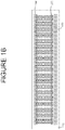
- Figure 1C shows a schematic top-view of a naturally closed ohmic MEMS switch-array. It contains a number of parallel operated switch-cells 110. The RF-electrodes 102 of each cell are connected together at one end of each switch-cell 110, while the anchor-electrodes 106 are connected together at the other end of each switch-cell 110. When all cells are turned on this results in a further reduction of the resistance between the RF-electrode 102 and anchor electrode 106. At the same time, because many switches are operated in parallel the total switch-array can handle more current. All switches can be turned off collectively by applying a high-enough voltage to the control-electrode.
- the contacting switch will provide a current path for protecting against ESD events at conditions during handling and assembly.
- the contacting switch is opened by applying a bias voltage.
- the residual capacitive coupling and leakage between the open switch terminals will be minimized by design. This way, the RF performance of the RF MEMS device that was protected is maintained almost fully intact. This is the greatest advantage compared to other traditional ESD protection techniques based on solid-state technology, which inevitably degrade the RF performance of the MEMS device to be protected.
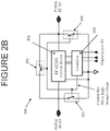
- FIGs2A and 2B show schematic drawings of the naturally closed MEMS switch 301 and of the way it is combined with an RF MEMS device 302 and controller 303 in one package 300 in order to provide ESD protection by providing a low resistance path between any pair of analog/RF IO's.
- the naturally closed switches are unpowered and the control voltage applied to control-line 304 is at 0V.
- the switches 301 provide a low-ohmic path between all the analog/RF IO's.
- the device 300 is turned on and the controller 303 applies a high-enough voltage on the control-line 304 which is connected to the control-electrodes of each switch 301.
- the switches 301 are now in the open-state and the analog/RF IO's are disconnected.
- the number of switches ( Figure 1A ) to use in each switch-cell ( Figure 1B ) and the number of switch-cells to use can be tuned depending on the required ESD-protection.
- MEMS technology switches have a standard configuration where by design an electric contact between two electrodes can be closed or opened by applying bias voltage to one or more terminals. Without applying any bias voltage (unbiased condition), the state of the electrical contact is either undefined or open.
- a new type of MEMS switch is described which is referred to as a "contacting" switch.
- the contacting switch presents a closed electrical contact between two electrodes even in the absence of applied bias voltage. This is achieved by specific mechanical design of the MEMS device, by managing the internal stress and strain conditions of the suspended MEMS membranes after the fabrication process is completed.
- FIG 3A shows a cross-section view of a naturally closed ohmic MEMS (contacting) switch 200 according to the invention.
- the contacting switch 200 contains an RF electrode 102 and anchor electrode 106 located on substrate 202.
- the substrate is covered with a dielectric layer 204 to protect other electrodes in different MEMS devices located on the same substrate.
- Suitable materials for the electrically insulating or dielectric layer 204 include silicon based materials including silicon-oxide, silicon-dioxide, silicon-nitride and silicon-oxynitride.
- the thickness of this layer 204 is typically in the range of 50nm to 150nm to limit the electric field in the dielectric layer.
- RF contact 206 On top of the RF electrode 102 is the RF contact 206 to which the switch body forms an ohmic contact in the closed state.
- anchor contact 208 On top of the anchor-electrode 106 is the anchor contact 208 to which the MEMS device is anchored.
- Typical materials used for the contacting layers 206, 208 include Ti, TiN, TiAl, TiAIN, AIN, Al, W, Pt, Ir, Rh, Ru, RuO 2 , ITO and Mo and combinations thereof.
- the switch element contains a cantilever consisting of conductive layers 210, 212 which are joined together near the RF-contact 206 using vias 214. Suspension legs 216 are formed in the lower layer 210 which reduce the voltage required to operate the switch.
- the MEMS cantilever is anchored to the substrate with via 222.
- a stress-layer 211 which has a higher tensile stress than the lower layer 210. This causes the cantilever beam to flex downward until it hits the RF-contact 206.
- the contact force that the cantilever exerts on the RF-contact can be tuned with the dimensions of the lower-layer 210 and the stress-layer 211 as well as with the stress in these layers.
- dielectric layer 224 which is capped with metal pull-up electrode 226 (the control-electrode) which is used to pull the MEMS up to the roof for the off state.
- Dielectric layer 224 avoids a short-circuit between the MEMS cantilever and the pull-up electrode 226 in the actuated-up state and limits the electric fields for high reliability. Moving the device to the top helps reduce the capacitance of the switch to the RF-electrode 102 in the off state.
- the cavity roof further contains an additional dielectric layer 228 for mechanical strength.
- the cavity is sealed with dielectric layer 230 which fills the etch release holes 232 used to remove the sacrificial layers which are present during fabrication.
- the dielectric layer 230 enters the etch release holes 232 and provides a further mechanical support to the top-layer 212 of the MEMS-cantilever in the anchors, while also sealing the cavity so that there is a low pressure environment in the cavity.
- Suitable materials for the roof dielectric layers 228, 230 include silicon based materials including silicon-oxide, silicon-dioxide, silicon-nitride and silicon-oxynitride.
- the upper layer 212 When the lower layer 210 is deflected downwards, the upper layer 212 is moved downwards at the location of via 214 as well. Because of the deflection angle of the lower layer 210 at this location, the upper layer near the location of the legs 216 moves up, which reduces the gap between the control-electrode and the upper layer 212. This allows the contacting switch to be opened with a relatively low potential applied to the roof electrode 226. If the length of the upper layer 212 is long enough, the upper layer 212 can touch the roof dielectric 224 near the location of the leg 216. This further reduces the voltage required to pull the cantilever intimately up with the roof.
- Figure 3B shows the device in the actuated off state.
- a high enough voltage is applied to the control-electrode 226, which pulls the MEMS cantilever 211, 212 up towards the roof, thereby disconnecting the RF-electrode 102 from the anchor electrode 106.
- the switch can be opened at one roof voltage for test after fabrication and then closed again to provide ESD protection to the packaged device until in use in the final application.
- the device By applying a higher voltage to the control-electrode, the device can be put permanently in the open-state, by zipping in the top-layer 212 on the top-dielectric 224 and increasing the contacting area. Stiction forces will hold the cantilever switch in the open-state.
- the mechanical design of the contacting switch is based on engineering of residual absolute and gradient stress within a suspended membrane at the end of the fabrication process. Depositing a stack of materials with different residual stress conditions results in a final built-in gradient stress, which leads to the desired deformation of the suspended membrane.
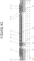
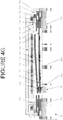
- Figures 4A-4G are schematic illustrations of the MEMS ohmic switch 200 at various stages of fabrication according to one embodiment.
- Figure 4A shows the backplane starting material of the MEMS-switch and contains a substrate 202 with a plurality of electrodes including the RF electrode 102 and the anchor electrodes 106.
- the substrate 202 may comprise a single layer substrate or a multi-layer substrate such as a CMOS substrate having one or more layers of interconnects.
- suitable materials that may be used for the electrodes 102, 106 include titanium-nitride, aluminum, tungsten, copper, titanium, and combinations thereof including multi-layer stacks of different material.
- the substrate is covered with an electrically insulating layer 204 to protect other electrodes of different devices located on the same substrate.
- Suitable materials for the electrically insulating layer 204 include silicon based materials including silicon-oxide, silicon-dioxide, silicon-nitride and silicon-oxynitride.
- RF contact 206 On top of the RF-electrode is RF contact 206 and on top of the anchor electrode 106 is anchor contact 208.
- Typical materials used for the contacts 206, 208 include Ti, TiN, TiAl, TiAIN, AIN, Al, W, Pt, Ir, Rh, Ru, RuO 2 , ITO and Mo and combinations thereof.
- Figure 4B shows the lower layer 210 of the MEMS cantilever which is formed on the backplane by depositing a sacrificial layer 302, depositing and patterning the stress layer 211, opening vias 222 in the sacrificial layer 302 and depositing and patterning the lower cantilever portion including the legs at 216.
- the MEMS cantilever is anchored to the anchor contact 208 with via 222 located on one side of the cantilever.
- the bottom side of stress layer 211 may be covered with an insulating layer which is partially removed over the RF-contact layer 206 to facilitate an ohmic contact to be made.
- Figure 4C shows the formation of the upper layer 212 of the MEMS cantilever. Additional sacrificial material 302 is deposited and openings are generated in in the locations of vias 220, 214 which land on the lower MEMS layer 210. The upper MEMS layer 212 is deposited and patterned to create the full MEMS cantilever 210, 211, 212 joined together by vias 214, containing legs 216 and anchor vias 220, 222.
- Figure 4D shows the formation of the pull-up electrode by depositing additional sacrificial material 302 and an insulating dielectric layer 224.
- Suitable materials for the electrically insulating layer 224 include silicon based materials including silicon-oxide, silicon-dioxide, silicon-nitride and silicon-oxynitride.
- the dielectric layer 224 and sacrificial material 302 are patterned to form the cavity outline, thereby exposing portions 238 of the lower MEMS-cantilever layer and 236 of the upper MEMS-cantilever layer as well as a portion of the anchor contact layer 208.
- Figure 4E shows the formation of the pull-up (control) electrode 226 as well as the sidewall electrical connections 234, which connects to the exposed portions 236 of the upper MEMS-cantilever layer, to exposed portions 238 of the lower MEMS-cantilever layer and to the anchor contact 208, thus providing an additional current path from the MEMS cantilever 210, 212 to the anchor contact 208 in parallel with the anchor vias 220, 222.
- Figure 4F shows the formation of the cavity roof, by depositing a dielectric material 228.
- Suitable materials for the electrically insulating layer 228 include silicon based materials including silicon-oxide, silicon-dioxide, silicon-nitride and silicon-oxynitride. This layer provides additional mechanical strength to the roof. Etch release holes 232 are opened which exposes the sacrificial material in the cavity.
- Figure 4G shows the MEMS switch after the sacrificial layer has been removed through the release holes 232 and sealed with dielectric layer 230.
- the dielectric layer 230 also is deposited inside the etch release holes 232 and lands on upper MEMS layer 212 providing additional mechanical strength to the anchors. Because the stress layer 211 has a higher tensile stress than the lower cantilever layer 210, the cantilever will deflect downwards until it hits the RF-contact 206 and the switch provides an ohmic contact between 102 and 106.
- a contacting switch By utilizing a contacting switch, ESD damage to other MEMS devices in the package is avoided.
- the contacting switch is naturally in the closed position and is opened upon applying a voltage. Hence, there is little to no damage to a MEMS device employing these ESD-protection devices.
Landscapes
- Micromachines (AREA)
- Engineering & Computer Science (AREA)
- Power Engineering (AREA)
Claims (15)
- Eine MEMS-Vorrichtung, die Folgendes umfasst:ein Substrat (202), das darin angeordnet eine Ankerelektrode (106) und eine HF-Elektrode (102) aufweist; undein Schaltelement (200), das eine Beanspruchungsschicht (211), eine untere Schicht (210) und eine obere Schicht (212) umfasst, wobei die untere Schicht (210) mit der obere Schicht (212) an einem ersten Ende gekoppelt ist und die untere Schicht (210) mit der Ankerelektrode (106) an dem zweiten Ende gekoppelt ist;dadurch gekennzeichnet, dass die Beanspruchungsschicht (211) unter Dehnbeanspruchung steht, wobei die Beanspruchungsschicht (211) mit einer unteren Oberfläche der unteren Schicht (210) in Kontakt steht, wobei die obere Schicht (212) von der unteren Schicht (210) an einer ersten Stelle beabstandet ist.
- MEMS-Vorrichtung nach Anspruch 1, die ferner einen Ankerkontakt (208) umfasst, der zwischen der Ankerelektrode (106) und der unteren Schicht (210) angeordnet ist.
- MEMS-Vorrichtung nach Anspruch 1, wobei das Schaltelement (200) in einer natürlich geschlossenen Position nach unten zu der RF-Elektrode (102) gebogen wird.
- MEMS-Vorrichtung nach Anspruch 1, die ferner einen RF-Kontakt (206) umfasst, der auf der RF-Elektrode (102) angeordnet ist, wobei sich die Beanspruchungsschicht (211) aus einer mit dem RF-Kontakt (206) in Kontakt stehenden Position und einer von dem RF-Kontakt (206) beabstandeten Position bewegt.
- MEMS-Vorrichtung nach Anspruch 4, die ferner eine Isolierschicht (204) umfasst, die auf einer unteren Oberfläche der Beanspruchungsschicht (211) angeordnet ist, wobei die Isolierschicht (204) eine Öffnung an einer Stelle aufweist, die dem RF-Kontakt (206) entspricht, sodass ein Abschnitt der Beanspruchungsschicht (211) exponiert ist, um einen Kontakt mit dem RF-Kontakt (206) herzustellen.
- MEMS-Vorrichtung nach Anspruch 1, wobei die Beanspruchung in der Beanspruchungsschicht (211) dehnender als die Beanspruchung in der unteren Schicht (210) ist.
- MEMS-Vorrichtung nach Anspruch 1, die ferner eine Isolierschicht (204) umfasst, die auf einer unteren Oberfläche der Beanspruchungsschicht (211) angeordnet ist, wobei die Isolierschicht (204) eine Öffnung an einer Stelle aufweist, die der RF-Elektrode (102) entspricht, sodass ein Abschnitt der Beanspruchungsschicht (211) exponiert ist.
- MEMS-Vorrichtung nach Anspruch 1, die ferner Folgendes umfasst:eine Pull-up-Elektrode (226), die über dem Schaltelement (200) angeordnet ist; undeine Isolierschicht (224), die zwischen der Pull-up-Elektrode (226) und der oberen Schicht (212) angeordnet ist, wobei die obere Schicht (212) mit der Isolierschicht (224) an der ersten Stelle gekoppelt ist und mit dieser in Kontakt steht.
- MEMS-Vorrichtung nach Anspruch 8, wobei die obere Schicht (212) mit der Isolierschicht (224) in Kontakt bleibt, wenn die Beanspruchungsschicht (211) mit einem RF-Kontakt (206) in Kontakt steht.
- MEMS-Vorrichtung nach Anspruch 8, wobei die obere Schicht (212) mit der unteren Schicht (210) an einer an die RF-Elektrode (102) angrenzenden Stelle gekoppelt ist.
- MEMS-Vorrichtung nach Anspruch 10, wobei sich das Schaltelement (200) um einen ersten Abstand von der RF-Elektrode (102) durch Anlegen einer ersten Spannung auf die Pull-up-Elektrode (226) weg bewegen kann.
- MEMS-Vorrichtung nach Anspruch 11, wobei sich das Schaltelement (200) um einen zweiten Abstand von der RF-Elektrode (102) weg bewegen kann, wenn eine zweite Spannung angelegt wird, wobei der zweite Abstand größer als der erste Abstand ist; wobei die zweite Spannung größer als die erste Spannung ist.
- MEMS-Vorrichtung nach Anspruch 12, wobei die obere Schicht (212), wenn an dem zweiten Abstand, mit der Isolierschicht (224) in Kontakt steht.
- MEMS-Vorrichtung nach Anspruch 13, wobei die obere Schicht (212) mit der Isolierschicht (224) in Kontakt bleibt und die Beanspruchungsschicht (211) von der RF-Elektrode (102) beabstandet bleibt, wenn die zweite Spannung entfernt wird.
- MEMS-Vorrichtung nach Anspruch 14, wobei die Beanspruchungsschicht (211) auf eine mit einem RF-Kontakt (206) in Kontakt stehende Position zurückkehrt, wenn die erste Spannung entfernt wird.
Applications Claiming Priority (2)
| Application Number | Priority Date | Filing Date | Title |
|---|---|---|---|
| US201562256045P | 2015-11-16 | 2015-11-16 | |
| PCT/US2016/061937 WO2017087341A1 (en) | 2015-11-16 | 2016-11-15 | Naturally closed mems switch for esd protection |
Publications (2)
| Publication Number | Publication Date |
|---|---|
| EP3378087A1 EP3378087A1 (de) | 2018-09-26 |
| EP3378087B1 true EP3378087B1 (de) | 2021-12-01 |
Family
ID=57442817
Family Applications (1)
| Application Number | Title | Priority Date | Filing Date |
|---|---|---|---|
| EP16804970.8A Active EP3378087B1 (de) | 2015-11-16 | 2016-11-15 | Natürlich geschlossener mems-schalter für schutz vor elektrostatischer entladung |
Country Status (6)
| Country | Link |
|---|---|
| US (1) | US10964505B2 (de) |
| EP (1) | EP3378087B1 (de) |
| JP (1) | JP6864684B2 (de) |
| KR (1) | KR102632493B1 (de) |
| CN (1) | CN108352277B (de) |
| WO (1) | WO2017087341A1 (de) |
Families Citing this family (7)
| Publication number | Priority date | Publication date | Assignee | Title |
|---|---|---|---|---|
| CN109411278A (zh) * | 2017-08-16 | 2019-03-01 | 致伸科技股份有限公司 | 防静电放电的按键结构 |
| KR102810891B1 (ko) * | 2017-12-13 | 2025-05-20 | 엔체인 홀딩스 리미티드 | 암호 자료를 안전하게 공유하기 위한 시스템 및 방법 |
| US11746002B2 (en) | 2019-06-22 | 2023-09-05 | Qorvo Us, Inc. | Stable landing above RF conductor in MEMS device |
| US11705298B2 (en) * | 2019-06-22 | 2023-07-18 | Qorvo Us, Inc. | Flexible MEMS device having hinged sections |
| US11667516B2 (en) | 2019-06-26 | 2023-06-06 | Qorvo Us, Inc. | MEMS device having uniform contacts |
| US11615924B2 (en) * | 2020-10-25 | 2023-03-28 | AAC Technologies Pte. Ltd. | MEMS switch |
| FR3138657A1 (fr) | 2022-08-08 | 2024-02-09 | Airmems | Commutateur MEMS à multiples déformations et commutateur comprenant un ou plusieurs commutateurs MEMS |
Family Cites Families (17)
| Publication number | Priority date | Publication date | Assignee | Title |
|---|---|---|---|---|
| US5638946A (en) * | 1996-01-11 | 1997-06-17 | Northeastern University | Micromechanical switch with insulated switch contact |
| DE19736674C1 (de) * | 1997-08-22 | 1998-11-26 | Siemens Ag | Mikromechanisches elektrostatisches Relais und Verfahren zu dessen Herstellung |
| US6127908A (en) * | 1997-11-17 | 2000-10-03 | Massachusetts Institute Of Technology | Microelectro-mechanical system actuator device and reconfigurable circuits utilizing same |
| US6046659A (en) * | 1998-05-15 | 2000-04-04 | Hughes Electronics Corporation | Design and fabrication of broadband surface-micromachined micro-electro-mechanical switches for microwave and millimeter-wave applications |
| CN1173398C (zh) * | 1999-02-04 | 2004-10-27 | 蒂科电子输给系统股份公司 | 微型继电器 |
| US6236491B1 (en) * | 1999-05-27 | 2001-05-22 | Mcnc | Micromachined electrostatic actuator with air gap |
| US6426687B1 (en) * | 2001-05-22 | 2002-07-30 | The Aerospace Corporation | RF MEMS switch |
| US6869169B2 (en) * | 2002-05-15 | 2005-03-22 | Eastman Kodak Company | Snap-through thermal actuator |
| US7101724B2 (en) * | 2004-02-20 | 2006-09-05 | Wireless Mems, Inc. | Method of fabricating semiconductor devices employing at least one modulation doped quantum well structure and one or more etch stop layers for accurate contact formation |
| US7372348B2 (en) * | 2004-08-20 | 2008-05-13 | Palo Alto Research Center Incorporated | Stressed material and shape memory material MEMS devices and methods for manufacturing |
| US20070236307A1 (en) * | 2006-04-10 | 2007-10-11 | Lianjun Liu | Methods and apparatus for a packaged MEMS switch |
| JP4234737B2 (ja) * | 2006-07-24 | 2009-03-04 | 株式会社東芝 | Memsスイッチ |
| JP2008210640A (ja) * | 2007-02-26 | 2008-09-11 | Murata Mfg Co Ltd | 静電駆動素子およびそれを備えた静電駆動デバイス |
| US7754986B1 (en) * | 2007-02-27 | 2010-07-13 | National Semiconductor Corporation | Mechanical switch that reduces the effect of contact resistance |
| JP2010129371A (ja) * | 2008-11-27 | 2010-06-10 | Toshiba Corp | スイッチ及びesd保護素子 |
| US9708177B2 (en) * | 2011-09-02 | 2017-07-18 | Cavendish Kinetics, Inc. | MEMS device anchoring |
| JP6397913B2 (ja) | 2013-08-01 | 2018-09-26 | キャベンディッシュ・キネティックス・インコーポレイテッドCavendish Kinetics, Inc. | Mems抵抗スイッチおよびmimキャパシタを利用したdvc |
-
2016
- 2016-11-15 EP EP16804970.8A patent/EP3378087B1/de active Active
- 2016-11-15 CN CN201680066444.2A patent/CN108352277B/zh active Active
- 2016-11-15 JP JP2018525370A patent/JP6864684B2/ja active Active
- 2016-11-15 US US15/772,132 patent/US10964505B2/en active Active
- 2016-11-15 WO PCT/US2016/061937 patent/WO2017087341A1/en not_active Ceased
- 2016-11-15 KR KR1020187016998A patent/KR102632493B1/ko active Active
Non-Patent Citations (1)
| Title |
|---|
| None * |
Also Published As
| Publication number | Publication date |
|---|---|
| CN108352277B (zh) | 2021-02-26 |
| JP2018535521A (ja) | 2018-11-29 |
| JP6864684B2 (ja) | 2021-04-28 |
| KR20180072837A (ko) | 2018-06-29 |
| US10964505B2 (en) | 2021-03-30 |
| CN108352277A (zh) | 2018-07-31 |
| WO2017087341A1 (en) | 2017-05-26 |
| KR102632493B1 (ko) | 2024-02-02 |
| EP3378087A1 (de) | 2018-09-26 |
| US20190066958A1 (en) | 2019-02-28 |
Similar Documents
| Publication | Publication Date | Title |
|---|---|---|
| EP3378087B1 (de) | Natürlich geschlossener mems-schalter für schutz vor elektrostatischer entladung | |
| JP6397913B2 (ja) | Mems抵抗スイッチおよびmimキャパシタを利用したdvc | |
| US6621135B1 (en) | Microrelays and microrelay fabrication and operating methods | |
| KR20010030305A (ko) | 접이식 스프링을 구비한 초소형 전기 기계 고주파 스위치및 그 제조 방법 | |
| KR102699850B1 (ko) | Mems rf 적용의 esd 보호 | |
| US20240150166A1 (en) | Encapsulated MEMS Switching Element, Device and Production Method | |
| EP3254294B1 (de) | Dvc mit verwendung von mims im anker | |
| EP3378080B1 (de) | Mems-vorrichtung und verfahren zur herstellung einer mems-vorrichtung | |
| JP6917370B2 (ja) | Rfスイッチの脚とアンカーにおける電流取り扱い | |
| KR100668614B1 (ko) | 압전 구동 방식 저항형 rf mems 스위치 및 그 제조방법 | |
| CN109314018A (zh) | 可变射频微机电开关 | |
| JP7193670B1 (ja) | Memsスイッチ | |
| US12394577B2 (en) | Two-stage actuation in MEMS ohmic relays |
Legal Events
| Date | Code | Title | Description |
|---|---|---|---|
| STAA | Information on the status of an ep patent application or granted ep patent |
Free format text: STATUS: UNKNOWN |
|
| STAA | Information on the status of an ep patent application or granted ep patent |
Free format text: STATUS: THE INTERNATIONAL PUBLICATION HAS BEEN MADE |
|
| PUAI | Public reference made under article 153(3) epc to a published international application that has entered the european phase |
Free format text: ORIGINAL CODE: 0009012 |
|
| STAA | Information on the status of an ep patent application or granted ep patent |
Free format text: STATUS: REQUEST FOR EXAMINATION WAS MADE |
|
| 17P | Request for examination filed |
Effective date: 20180510 |
|
| AK | Designated contracting states |
Kind code of ref document: A1 Designated state(s): AL AT BE BG CH CY CZ DE DK EE ES FI FR GB GR HR HU IE IS IT LI LT LU LV MC MK MT NL NO PL PT RO RS SE SI SK SM TR |
|
| AX | Request for extension of the european patent |
Extension state: BA ME |
|
| DAV | Request for validation of the european patent (deleted) | ||
| DAX | Request for extension of the european patent (deleted) | ||
| STAA | Information on the status of an ep patent application or granted ep patent |
Free format text: STATUS: EXAMINATION IS IN PROGRESS |
|
| 17Q | First examination report despatched |
Effective date: 20200504 |
|
| GRAP | Despatch of communication of intention to grant a patent |
Free format text: ORIGINAL CODE: EPIDOSNIGR1 |
|
| STAA | Information on the status of an ep patent application or granted ep patent |
Free format text: STATUS: GRANT OF PATENT IS INTENDED |
|
| RIC1 | Information provided on ipc code assigned before grant |
Ipc: H01H 59/00 20060101AFI20210511BHEP Ipc: H01H 1/00 20060101ALI20210511BHEP |
|
| INTG | Intention to grant announced |
Effective date: 20210604 |
|
| RAP3 | Party data changed (applicant data changed or rights of an application transferred) |
Owner name: CAVENDISH KINETICS, INC. |
|
| GRAS | Grant fee paid |
Free format text: ORIGINAL CODE: EPIDOSNIGR3 |
|
| GRAA | (expected) grant |
Free format text: ORIGINAL CODE: 0009210 |
|
| STAA | Information on the status of an ep patent application or granted ep patent |
Free format text: STATUS: THE PATENT HAS BEEN GRANTED |
|
| AK | Designated contracting states |
Kind code of ref document: B1 Designated state(s): AL AT BE BG CH CY CZ DE DK EE ES FI FR GB GR HR HU IE IS IT LI LT LU LV MC MK MT NL NO PL PT RO RS SE SI SK SM TR |
|
| REG | Reference to a national code |
Ref country code: GB Ref legal event code: FG4D |
|
| REG | Reference to a national code |
Ref country code: AT Ref legal event code: REF Ref document number: 1452601 Country of ref document: AT Kind code of ref document: T Effective date: 20211215 Ref country code: CH Ref legal event code: EP |
|
| REG | Reference to a national code |
Ref country code: IE Ref legal event code: FG4D |
|
| REG | Reference to a national code |
Ref country code: DE Ref legal event code: R096 Ref document number: 602016066887 Country of ref document: DE |
|
| REG | Reference to a national code |
Ref country code: LT Ref legal event code: MG9D |
|
| REG | Reference to a national code |
Ref country code: NL Ref legal event code: MP Effective date: 20211201 |
|
| REG | Reference to a national code |
Ref country code: AT Ref legal event code: MK05 Ref document number: 1452601 Country of ref document: AT Kind code of ref document: T Effective date: 20211201 |
|
| PG25 | Lapsed in a contracting state [announced via postgrant information from national office to epo] |
Ref country code: RS Free format text: LAPSE BECAUSE OF FAILURE TO SUBMIT A TRANSLATION OF THE DESCRIPTION OR TO PAY THE FEE WITHIN THE PRESCRIBED TIME-LIMIT Effective date: 20211201 Ref country code: LT Free format text: LAPSE BECAUSE OF FAILURE TO SUBMIT A TRANSLATION OF THE DESCRIPTION OR TO PAY THE FEE WITHIN THE PRESCRIBED TIME-LIMIT Effective date: 20211201 Ref country code: FI Free format text: LAPSE BECAUSE OF FAILURE TO SUBMIT A TRANSLATION OF THE DESCRIPTION OR TO PAY THE FEE WITHIN THE PRESCRIBED TIME-LIMIT Effective date: 20211201 Ref country code: BG Free format text: LAPSE BECAUSE OF FAILURE TO SUBMIT A TRANSLATION OF THE DESCRIPTION OR TO PAY THE FEE WITHIN THE PRESCRIBED TIME-LIMIT Effective date: 20220301 Ref country code: AT Free format text: LAPSE BECAUSE OF FAILURE TO SUBMIT A TRANSLATION OF THE DESCRIPTION OR TO PAY THE FEE WITHIN THE PRESCRIBED TIME-LIMIT Effective date: 20211201 |
|
| PG25 | Lapsed in a contracting state [announced via postgrant information from national office to epo] |
Ref country code: SE Free format text: LAPSE BECAUSE OF FAILURE TO SUBMIT A TRANSLATION OF THE DESCRIPTION OR TO PAY THE FEE WITHIN THE PRESCRIBED TIME-LIMIT Effective date: 20211201 Ref country code: PL Free format text: LAPSE BECAUSE OF FAILURE TO SUBMIT A TRANSLATION OF THE DESCRIPTION OR TO PAY THE FEE WITHIN THE PRESCRIBED TIME-LIMIT Effective date: 20211201 Ref country code: NO Free format text: LAPSE BECAUSE OF FAILURE TO SUBMIT A TRANSLATION OF THE DESCRIPTION OR TO PAY THE FEE WITHIN THE PRESCRIBED TIME-LIMIT Effective date: 20220301 Ref country code: LV Free format text: LAPSE BECAUSE OF FAILURE TO SUBMIT A TRANSLATION OF THE DESCRIPTION OR TO PAY THE FEE WITHIN THE PRESCRIBED TIME-LIMIT Effective date: 20211201 Ref country code: HR Free format text: LAPSE BECAUSE OF FAILURE TO SUBMIT A TRANSLATION OF THE DESCRIPTION OR TO PAY THE FEE WITHIN THE PRESCRIBED TIME-LIMIT Effective date: 20211201 Ref country code: GR Free format text: LAPSE BECAUSE OF FAILURE TO SUBMIT A TRANSLATION OF THE DESCRIPTION OR TO PAY THE FEE WITHIN THE PRESCRIBED TIME-LIMIT Effective date: 20220302 Ref country code: ES Free format text: LAPSE BECAUSE OF FAILURE TO SUBMIT A TRANSLATION OF THE DESCRIPTION OR TO PAY THE FEE WITHIN THE PRESCRIBED TIME-LIMIT Effective date: 20211201 |
|
| PG25 | Lapsed in a contracting state [announced via postgrant information from national office to epo] |
Ref country code: NL Free format text: LAPSE BECAUSE OF FAILURE TO SUBMIT A TRANSLATION OF THE DESCRIPTION OR TO PAY THE FEE WITHIN THE PRESCRIBED TIME-LIMIT Effective date: 20211201 |
|
| PG25 | Lapsed in a contracting state [announced via postgrant information from national office to epo] |
Ref country code: SM Free format text: LAPSE BECAUSE OF FAILURE TO SUBMIT A TRANSLATION OF THE DESCRIPTION OR TO PAY THE FEE WITHIN THE PRESCRIBED TIME-LIMIT Effective date: 20211201 Ref country code: SK Free format text: LAPSE BECAUSE OF FAILURE TO SUBMIT A TRANSLATION OF THE DESCRIPTION OR TO PAY THE FEE WITHIN THE PRESCRIBED TIME-LIMIT Effective date: 20211201 Ref country code: RO Free format text: LAPSE BECAUSE OF FAILURE TO SUBMIT A TRANSLATION OF THE DESCRIPTION OR TO PAY THE FEE WITHIN THE PRESCRIBED TIME-LIMIT Effective date: 20211201 Ref country code: PT Free format text: LAPSE BECAUSE OF FAILURE TO SUBMIT A TRANSLATION OF THE DESCRIPTION OR TO PAY THE FEE WITHIN THE PRESCRIBED TIME-LIMIT Effective date: 20220401 Ref country code: EE Free format text: LAPSE BECAUSE OF FAILURE TO SUBMIT A TRANSLATION OF THE DESCRIPTION OR TO PAY THE FEE WITHIN THE PRESCRIBED TIME-LIMIT Effective date: 20211201 Ref country code: CZ Free format text: LAPSE BECAUSE OF FAILURE TO SUBMIT A TRANSLATION OF THE DESCRIPTION OR TO PAY THE FEE WITHIN THE PRESCRIBED TIME-LIMIT Effective date: 20211201 |
|
| REG | Reference to a national code |
Ref country code: DE Ref legal event code: R081 Ref document number: 602016066887 Country of ref document: DE Owner name: QORVO US, INC., GREENSBORO, US Free format text: FORMER OWNER: CAVENDISH KINETICS, INC., SAN JOSE, CA, US |
|
| REG | Reference to a national code |
Ref country code: DE Ref legal event code: R097 Ref document number: 602016066887 Country of ref document: DE |
|
| REG | Reference to a national code |
Ref country code: GB Ref legal event code: 732E Free format text: REGISTERED BETWEEN 20220811 AND 20220817 |
|
| PG25 | Lapsed in a contracting state [announced via postgrant information from national office to epo] |
Ref country code: IS Free format text: LAPSE BECAUSE OF FAILURE TO SUBMIT A TRANSLATION OF THE DESCRIPTION OR TO PAY THE FEE WITHIN THE PRESCRIBED TIME-LIMIT Effective date: 20220401 |
|
| PLBE | No opposition filed within time limit |
Free format text: ORIGINAL CODE: 0009261 |
|
| STAA | Information on the status of an ep patent application or granted ep patent |
Free format text: STATUS: NO OPPOSITION FILED WITHIN TIME LIMIT |
|
| PG25 | Lapsed in a contracting state [announced via postgrant information from national office to epo] |
Ref country code: DK Free format text: LAPSE BECAUSE OF FAILURE TO SUBMIT A TRANSLATION OF THE DESCRIPTION OR TO PAY THE FEE WITHIN THE PRESCRIBED TIME-LIMIT Effective date: 20211201 Ref country code: AL Free format text: LAPSE BECAUSE OF FAILURE TO SUBMIT A TRANSLATION OF THE DESCRIPTION OR TO PAY THE FEE WITHIN THE PRESCRIBED TIME-LIMIT Effective date: 20211201 |
|
| 26N | No opposition filed |
Effective date: 20220902 |
|
| PG25 | Lapsed in a contracting state [announced via postgrant information from national office to epo] |
Ref country code: SI Free format text: LAPSE BECAUSE OF FAILURE TO SUBMIT A TRANSLATION OF THE DESCRIPTION OR TO PAY THE FEE WITHIN THE PRESCRIBED TIME-LIMIT Effective date: 20211201 |
|
| PG25 | Lapsed in a contracting state [announced via postgrant information from national office to epo] |
Ref country code: IT Free format text: LAPSE BECAUSE OF FAILURE TO SUBMIT A TRANSLATION OF THE DESCRIPTION OR TO PAY THE FEE WITHIN THE PRESCRIBED TIME-LIMIT Effective date: 20211201 |
|
| P01 | Opt-out of the competence of the unified patent court (upc) registered |
Effective date: 20230515 |
|
| PG25 | Lapsed in a contracting state [announced via postgrant information from national office to epo] |
Ref country code: MC Free format text: LAPSE BECAUSE OF FAILURE TO SUBMIT A TRANSLATION OF THE DESCRIPTION OR TO PAY THE FEE WITHIN THE PRESCRIBED TIME-LIMIT Effective date: 20211201 |
|
| REG | Reference to a national code |
Ref country code: CH Ref legal event code: PL |
|
| REG | Reference to a national code |
Ref country code: BE Ref legal event code: MM Effective date: 20221130 |
|
| PG25 | Lapsed in a contracting state [announced via postgrant information from national office to epo] |
Ref country code: LI Free format text: LAPSE BECAUSE OF NON-PAYMENT OF DUE FEES Effective date: 20221130 Ref country code: CH Free format text: LAPSE BECAUSE OF NON-PAYMENT OF DUE FEES Effective date: 20221130 |
|
| PG25 | Lapsed in a contracting state [announced via postgrant information from national office to epo] |
Ref country code: LU Free format text: LAPSE BECAUSE OF NON-PAYMENT OF DUE FEES Effective date: 20221115 |
|
| PG25 | Lapsed in a contracting state [announced via postgrant information from national office to epo] |
Ref country code: IE Free format text: LAPSE BECAUSE OF NON-PAYMENT OF DUE FEES Effective date: 20221115 |
|
| PG25 | Lapsed in a contracting state [announced via postgrant information from national office to epo] |
Ref country code: BE Free format text: LAPSE BECAUSE OF NON-PAYMENT OF DUE FEES Effective date: 20221130 |
|
| PG25 | Lapsed in a contracting state [announced via postgrant information from national office to epo] |
Ref country code: HU Free format text: LAPSE BECAUSE OF FAILURE TO SUBMIT A TRANSLATION OF THE DESCRIPTION OR TO PAY THE FEE WITHIN THE PRESCRIBED TIME-LIMIT; INVALID AB INITIO Effective date: 20161115 |
|
| PG25 | Lapsed in a contracting state [announced via postgrant information from national office to epo] |
Ref country code: CY Free format text: LAPSE BECAUSE OF FAILURE TO SUBMIT A TRANSLATION OF THE DESCRIPTION OR TO PAY THE FEE WITHIN THE PRESCRIBED TIME-LIMIT Effective date: 20211201 |
|
| PG25 | Lapsed in a contracting state [announced via postgrant information from national office to epo] |
Ref country code: MK Free format text: LAPSE BECAUSE OF FAILURE TO SUBMIT A TRANSLATION OF THE DESCRIPTION OR TO PAY THE FEE WITHIN THE PRESCRIBED TIME-LIMIT Effective date: 20211201 |
|
| PG25 | Lapsed in a contracting state [announced via postgrant information from national office to epo] |
Ref country code: TR Free format text: LAPSE BECAUSE OF FAILURE TO SUBMIT A TRANSLATION OF THE DESCRIPTION OR TO PAY THE FEE WITHIN THE PRESCRIBED TIME-LIMIT Effective date: 20211201 |
|
| PG25 | Lapsed in a contracting state [announced via postgrant information from national office to epo] |
Ref country code: MT Free format text: LAPSE BECAUSE OF FAILURE TO SUBMIT A TRANSLATION OF THE DESCRIPTION OR TO PAY THE FEE WITHIN THE PRESCRIBED TIME-LIMIT Effective date: 20211201 |
|
| PGFP | Annual fee paid to national office [announced via postgrant information from national office to epo] |
Ref country code: DE Payment date: 20251022 Year of fee payment: 10 |
|
| PGFP | Annual fee paid to national office [announced via postgrant information from national office to epo] |
Ref country code: GB Payment date: 20251023 Year of fee payment: 10 |
|
| PGFP | Annual fee paid to national office [announced via postgrant information from national office to epo] |
Ref country code: FR Payment date: 20251022 Year of fee payment: 10 |