EP3378080B1 - Mems-vorrichtung und verfahren zur herstellung einer mems-vorrichtung - Google Patents
Mems-vorrichtung und verfahren zur herstellung einer mems-vorrichtung Download PDFInfo
- Publication number
- EP3378080B1 EP3378080B1 EP16804968.2A EP16804968A EP3378080B1 EP 3378080 B1 EP3378080 B1 EP 3378080B1 EP 16804968 A EP16804968 A EP 16804968A EP 3378080 B1 EP3378080 B1 EP 3378080B1
- Authority
- EP
- European Patent Office
- Prior art keywords
- electrode
- contact
- contact layer
- anchor
- layer
- Prior art date
- Legal status (The legal status is an assumption and is not a legal conclusion. Google has not performed a legal analysis and makes no representation as to the accuracy of the status listed.)
- Active
Links
Images



Classifications
-
- H—ELECTRICITY
- H01—ELECTRIC ELEMENTS
- H01H—ELECTRIC SWITCHES; RELAYS; SELECTORS; EMERGENCY PROTECTIVE DEVICES
- H01H1/00—Contacts
- H01H1/0036—Switches making use of microelectromechanical systems [MEMS]
-
- B—PERFORMING OPERATIONS; TRANSPORTING
- B81—MICROSTRUCTURAL TECHNOLOGY
- B81B—MICROSTRUCTURAL DEVICES OR SYSTEMS, e.g. MICROMECHANICAL DEVICES
- B81B3/00—Devices comprising flexible or deformable elements, e.g. comprising elastic tongues or membranes
- B81B3/0018—Structures acting upon the moving or flexible element for transforming energy into mechanical movement or vice versa, i.e. actuators, sensors, generators
- B81B3/0021—Transducers for transforming electrical into mechanical energy or vice versa
-
- B—PERFORMING OPERATIONS; TRANSPORTING
- B81—MICROSTRUCTURAL TECHNOLOGY
- B81C—PROCESSES OR APPARATUS SPECIALLY ADAPTED FOR THE MANUFACTURE OR TREATMENT OF MICROSTRUCTURAL DEVICES OR SYSTEMS
- B81C1/00—Manufacture or treatment of devices or systems in or on a substrate
- B81C1/00015—Manufacture or treatment of devices or systems in or on a substrate for manufacturing microsystems
- B81C1/00134—Manufacture or treatment of devices or systems in or on a substrate for manufacturing microsystems comprising flexible or deformable structures
- B81C1/00142—Bridges
-
- H—ELECTRICITY
- H01—ELECTRIC ELEMENTS
- H01H—ELECTRIC SWITCHES; RELAYS; SELECTORS; EMERGENCY PROTECTIVE DEVICES
- H01H59/00—Electrostatic relays; Electro-adhesion relays
-
- B—PERFORMING OPERATIONS; TRANSPORTING
- B81—MICROSTRUCTURAL TECHNOLOGY
- B81B—MICROSTRUCTURAL DEVICES OR SYSTEMS, e.g. MICROMECHANICAL DEVICES
- B81B2201/00—Specific applications of microelectromechanical systems
- B81B2201/01—Switches
- B81B2201/012—Switches characterised by the shape
- B81B2201/016—Switches characterised by the shape having a bridge fixed on two ends and connected to one or more dimples
-
- H—ELECTRICITY
- H01—ELECTRIC ELEMENTS
- H01H—ELECTRIC SWITCHES; RELAYS; SELECTORS; EMERGENCY PROTECTIVE DEVICES
- H01H1/00—Contacts
- H01H1/0036—Switches making use of microelectromechanical systems [MEMS]
- H01H2001/0084—Switches making use of microelectromechanical systems [MEMS] with perpendicular movement of the movable contact relative to the substrate
Definitions
- Embodiments of the present disclosure generally relate to a technique for improving the current handling of the RF-contact in MEMS switches.
- a MEMS resistive switch contains a movable plate that moves by applying a voltage to an actuation electrode. Once the electrode voltage reaches a certain voltage oftentimes referred to as a snap-in voltage, the plate moves towards the electrode. The plate moves back to the original position once the voltage is lowered to a release voltage.
- the release voltage is typically lower than the snap-in voltage due to the higher electrostatic forces when the plate is close to the actuation electrode and due to stiction between the plate and the surface to which the plate is in contact once moved closer to the electrode.
- the spring constant of the MEMS device sets the value of the pull in voltage and pull off voltage.
- the plate When the plate is actuated down, it lands on a contact electrode to which it makes an ohmic contact. To achieve a low repeatable contact resistance a high contact force is required between the plate and the contact-electrode. To achieve this contact force at reasonable operating voltages, the gap between the plate and the pull-down electrode in the landed state needs to be small. As a result the contact electrode is typically a thin metal layer. This thin contact layer typically is connected to an underlying RF-electrode through a step-down via.
- WO 2015/017743 relates to a radio frequency (RF) digital variable capacitor (DVC) units for RF tuning and impedance matching.
- RF radio frequency
- DVC digital variable capacitor
- the present disclosure generally relates to a modified RF-contact design that does not suffer from a high current running through the thin sidewall in the via connection between the RF-contact and the underlying RF-electrode.
- the present invention refers to a MEMS device comprising a substrate having a plurality of electrodes formed therein, wherein the plurality of electrodes includes at least an anchor electrode, a pull-down electrode and an RF electrode; an insulating layer disposed over the substrate and the plurality of electrodes, wherein the insulating layer has a first opening formed therethrough to expose the anchor electrode and a second opening formed therethrough to expose the RF electrode; a contact layer that is electrically conductive, wherein the contact layer includes a first portion disposed within the first opening and in contact with the anchor electrode, a second portion disposed within the second opening and in contact with the RF electrode; a switching element disposed over the insulating layer, wherein the switching element includes an anchor portion in contact with the first portion of the contact layer, a leg portion and a bridge portion and wherein the bridge portion is movable from a first position spaced from the second portion of the contact layer and a second position in contact with the second portion of the contact layer, characterized in that the first portion
- Both the contact layer and the anchor electrode may comprise electrically conductive material and the contact layer and the anchor electrode may comprise different materials.
- the anchor electrode may have a first width and the first portion of the contact layer may have a second width, wherein the first width is greater than the second width.
- the first portion of the contact layer may have a thickness that is greater than a thickness of the insulating layer.
- the present invention also refers to a method of fabrication according of a MEMS device, comprising depositing an insulating layer over a substrate, the substrate having a plurality of electrodes formed therein, wherein the plurality of electrodes includes at least an anchor electrode, a pull-in electrode and an RF electrode; removing at least a portion of the insulating layer to form a first opening that exposes at least a portion of the anchor electrode and to form a second opening that exposes at least a portion of the RF electrode; depositing a contact layer over the insulating layer and within the first opening on the anchor electrode and within the second opening on the RF electrode; removing a portion of the contact layer, wherein a first portion remains within the first opening on the anchor electrode and wherein a second portion remains within the second opening on the RF electrode; forming a switching element over the substrate, wherein the switching element includes an anchor portion that is coupled to the first portion of the contact layer, wherein the switching element also includes a leg portion and bridge portion, wherein the switching element is
- Both the contact layer and the anchor electrode may comprise electrically conductive material and the contact layer and the anchor electrode may comprise different materials.
- the anchor electrode may have a first width and the first portion of the contact layer may have a second width, wherein the first width is greater than the second width.
- the present disclosure generally relates to a modified RF-contact design that does not suffer from a high current running through the thin sidewall in the via connection between the RF-contact and the underlying RF-electrode.
- Figure 1 shows a cross-section view of an ohmic MEMS switch 100.
- the switch 100 contains an RF electrode 102, pull-down electrodes 104 and anchor electrodes 106 located on substrate 101.
- the electrodes are covered with a dielectric layer 107 to avoid a short-circuit between the MEMS switch and the pull-down electrode in the pulled-down state.
- Suitable materials for the electrically insulating layer 107 include silicon based materials including silicon-oxide, silicon-dioxide, silicon-nitride and silicon-oxynitride.
- the thickness of the insulating layer 107 is typically in the range of 50nm to 150nm to limit the electric field in the insulating layer 107.
- the switch element contains a stiff bridge consisting of conductive layers 112, 114 which are joined together using an array of vias 116. This allows for a stiff plate-section and compliant legs to provide a high contact-force while keeping the operating voltage to acceptable levels.
- the MEMS bridge is suspended by legs 118 formed in the lower layer 112 and/or in the upper layer 114 of the MEMS bridge and anchored with via 120 onto conductor 110 which is connected to the anchor electrode 106 through a via opening 111 in the insulating layer 107.
- dielectric layer 126 Above the MEMS bridge there is a dielectric layer 126 which is capped with metal 122 which is used to pull the MEMS up to the roof for the off state.
- Dielectric layer 120 avoids a short-circuit between the MEMS bridge and the pull-up electrode in the actuated-up state and limits the electric fields for high reliability. Moving the device to the top helps reduce the capacitance of the switch in the off state.
- the cavity is sealed with dielectric layer 124 which fills the etch holes used to remove the sacrificial layers. It enters these holes and helps support the ends of the cantilevers, while also sealing the cavity so that there is a low pressure environment in the cavities.
- RF contact 108 is conductive and makes ohmic contact with the conducting underside of the MEMS plate 112 once the device is pulled down by applying a high-enough voltage on the pull-down electrode 104.
- Typical materials used for the RF contact 108 and conductor 110 include Ti, TiN, TiAl, TiAIN, AIN, Al, W, Pt, Ir, Rh, Ru, RuO 2 , ITO and Mo and combinations thereof.
- the conducting layer is typically thin in the 30nm to 100nm range, so that once the plate 112 is landed on the contact it is close to the pull-down electrode.
- the thin conducting layer will also have a thin sidewall inside the via opening 109 which connects it to the RF-electrode 102 located underneath the RF contact 108. Because the RF contact 108 is so thin, when running a high-current through the RF contact 108, this can lead to a failure of the RF contact 108.
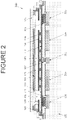
- FIG. 2 shows a cross-section view of an ohmic MEMS switch 200 according to one embodiment.
- the switch 200 contains an improved RF contact 202 which sits directly on top of the RF electrode 102 and an improved anchor contact 204 which sits directly on top of the anchor electrode 106. This is achieved by sizing the via opening 109 to be larger than the RF contact 202 and by sizing the via opening 111 to be larger than the anchor contact 204.
- the thickness of the RF contact 202 and anchor contact 204 now has to be increased by the thickness of the dielectric layer 107, so that these contacts protrude by the same amount over the dielectric layer 107 as in Figure 1 .
- Any current injected into these thicker contacts now has a path straight down to the underlying electrodes 102, 106 without having to travel through a thin sidewall. This improves the reliability of the RF contacts which now can handle more current.
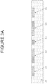
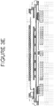
- FIGS 3A-3E are schematic illustrations of the MEMS ohmic switch at various stages of fabrication according to one embodiment.
- the substrate 101 has a plurality of electrodes including the RF electrode 102, pull-down electrodes 104 and the anchor electrodes 106 formed therein.
- the substrate 101 may comprise a single layer substrate or a multi-layer substrate such as a CMOS substrate having one or more layers of interconnects.
- suitable materials that may be used for the electrodes 102, 104, 106 include titanium-nitride, aluminum, tungsten, copper, titanium, and combinations thereof including multi-layer stacks of different material.
- an electrically insulating layer 107 is then deposited over the electrodes 102, 104, 106.
- Suitable materials for the electrically insulating layer 107 include silicon based materials including silicon-oxide, silicon-dioxide, silicon-nitride and silicon-oxynitride.
- the anchor electrode 106 has a width shown by arrows "A”
- the RF electrode 102 has a width as shown by arrow "B”.
- the electrically insulating layer 107 is removed over the RF electrode 102 and over portions of the anchor electrode 106 to create openings 109, 111.
- the opening is smaller than the underlying electrode, such as opening 111 shown above electrode 106 as arrows "C"
- the dielectric etch that removes the insulating layer 107 will stop on the underlying electrode 106.
- the dielectric etch that removes the insulating layer 107 will also etch a little bit extra dielectric located next to the electrode 102 as shown by item 302 so that the RF electrode 102, and ultimately the RF contact 202, are spaced from the dielectric layer 107.
- the RF contact 202 and anchor contact 204 are formed by deposition and patterning of a suitable conductive material required to provide a good ohmic contact to the MEMS switch fabricated above it in a later stage.
- Typical materials used for the RF contact 202 and anchor contact 204 include Ti, TiN, TiAl, TiAIN, AIN, Al, W, Pt, Ir, Rh, Ru, RuO 2 , ITO and Mo and combinations thereof.
- the width of the RF contact 202 and anchor contact 204 is typically smaller than the underlying electrode 102, 106 as shown by arrows "E" and "F".
- the thickness of the RF contact 202 and anchor contact 204 is greater than the thickness of the insulating layer 107 shown by arrows "H".
- 106 is etched as shown by arrows "I" such that the anchor electrode 106 and the RF electrode 102 have a first thickness at the location of the anchor contact 204 and RF contact 202 respectively and a second thickness adjacent the contacts 202, 204, but since the thickness of the RF contact 202 and anchor contact 204 is much less than the thickness of the underlying electrodes 102, 106 this poses no problem in the controllability of the process.
- the switch Due to the direct connection between the RF contact and the RF electrode, the switch does not suffer from a high current running through the thin sidewall.
- the switch is robust and not prone to failure.
Landscapes
- Engineering & Computer Science (AREA)
- Microelectronics & Electronic Packaging (AREA)
- Manufacturing & Machinery (AREA)
- Physics & Mathematics (AREA)
- Electromagnetism (AREA)
- Chemical & Material Sciences (AREA)
- Analytical Chemistry (AREA)
- Computer Hardware Design (AREA)
- Micromachines (AREA)
Claims (7)
- MEMS-Vorrichtung (200), Folgendes umfassend:ein Substrat (101) mit mehreren Elektroden, die darin ausgebildet sind, wobei die mehreren Elektroden mindestens eine Ankerelektrode (106), eine Pull-down-Elektrode (104) und eine HF-Elektrode (102) umfassen;eine Isolierschicht (107), die über dem Substrat und den mehreren Elektroden angeordnet ist, wobei die Isolierschicht eine erste Öffnung (111), die durch diese hindurch ausgebildet ist, um die Ankerelektrode (106) zu exponieren, und eine zweite Öffnung (109) aufweist, die durch diese hindurch ausgebildet ist, um die HF-Elektrode (102) zu exponieren;eine Kontaktschicht, die elektrisch leitend ist, wobei die Kontaktschicht einen ersten Abschnitt (204), der in der ersten Öffnung (111) angeordnet ist und mit der Ankerelektrode (106) in Kontakt steht, einen zweiten Abschnitt (202) umfasst, der in der zweiten Öffnung (109) angeordnet ist und mit der HF-Elektrode (102) in Kontakt steht; undein Schaltelement, das über der Isolierschicht (107) angeordnet ist, wobei das Schaltelement einen Ankerabschnitt (120), der mit dem ersten Abschnitt (204) der Kontaktschicht in Kontakt steht, einen Zweigabschnitt (118) und einen Brückenabschnitt (112) umfasst und wobei der Brückenabschnitt aus einer ersten Position, die von dem zweiten Abschnitt (202) der Kontaktschicht beabstandet ist, und einer zweiten Position beweglich ist, die mit dem zweiten Abschnitt (202) der Kontaktschicht in Kontakt steht,dadurch gekennzeichnet, dassder erste Abschnitt (204) der Kontaktschicht von der Isolierschicht (107) beabstandet ist; unddadurch, dass die HF-Elektrode (102) eine erste Höhe an einem Ort, der dem zweiten Abschnitt der Kontaktschicht benachbart ist, und eine zweite Höhe an einem Ort aufweist, der mit dem zweiten Abschnitt der Kontaktschicht in Kontakt steht, wobei die zweite Höhe größer ist als die erste Höhe.
- MEMS-Vorrichtung nach Anspruch 1, wobei sowohl die Kontaktschicht als auch die Ankerelektrode (106) elektrisch leitendes Material umfassen und wobei die Kontaktschicht und die Ankerelektrode verschiedene Materialien umfassen.
- MEMS-Vorrichtung nach Anspruch 1, wobei die Ankerelektrode (106) eine erste Breite aufweist und der erste Abschnitt (204) der Kontaktschicht eine zweite Breite aufweist und wobei die erste Breite größer ist als die zweite Breite.
- MEMS-Vorrichtung nach Anspruch 1, wobei der erste Abschnitt (204) der Kontaktschicht eine Dicke aufweist, die größer ist als eine Dicke der Isolierschicht (107).
- Verfahren zum Herstellen einer MEMS-Vorrichtung (200), Folgendes umfassend:Ablagern einer Isolierschicht (107) über einem Substrat (101), wobei das Substrat mehrere Elektroden aufweist, die darin ausgebildet sind, wobei die mehreren Elektroden mindestens eine Ankerelektrode (106), eine Pull-in-Elektrode (104) und eine HF-Elektrode (102) umfassen;Entfernen mindestens eines Abschnitts der Isolierschicht (107), um eine erste Öffnung (111) auszubilden, die mindestens einen Abschnitt der Ankerelektrode (106) exponiert, und um eine zweite Öffnung (109) auszubilden, die mindestens einen Abschnitt der HF-Elektrode (102) exponiert;Ablagern einer Kontaktschicht über der Isolierschicht (107) und in der ersten Öffnung (111) auf der Ankerelektrode (106) und in der zweiten Öffnung (109) auf der HF-Elektrode (102);Entfernen eines Abschnitts der Kontaktschicht, wobei ein erster Abschnitt (204) in der ersten Öffnung (111) auf der Ankerelektrode (106) verbleibt und wobei ein zweiter Abschnitt (202) in der zweiten Öffnung (109) auf der HF-Elektrode (102) verbleibt; undAusbilden eines Schaltelements über dem Substrat (101), wobei das Schaltelement einen Ankerabschnitt (120) umfasst, der mit dem ersten Abschnitt (204) der Kontaktschicht verbunden ist, wobei das Schaltelement auch einen Zweigabschnitt (118) und einen Brückenabschnitt (112) umfasst, wobei das Schaltelement aus einer ersten Position, die von dem zweiten Abschnitt (202) der Kontaktschicht beabstandet ist, und aus einer zweiten Position beweglich ist, die mit dem zweiten Abschnitt (202) der Kontaktschicht in Kontakt steht,dadurch gekennzeichnet, dassder erste Abschnitt (204) der Kontaktschicht von der Isolierschicht (107) beabstandet ist; unddadurch, dass die HF-Elektrode (102) eine erste Höhe an einem Ort, der dem zweiten Abschnitt der Kontaktschicht benachbart ist, und eine zweite Höhe an einem Ort aufweist, der mit dem zweiten Abschnitt der Kontaktschicht in Kontakt steht, wobei die zweite Höhe größer ist als die erste Höhe.
- Verfahren nach Anspruch 5, wobei sowohl die Kontaktschicht als auch die Ankerelektrode (106) elektrisch leitendes Material umfassen und wobei die Kontaktschicht und die Ankerelektrode (106) verschiedene Materialien umfassen.
- Verfahren nach Anspruch 5, wobei die Ankerelektrode (102) eine erste Breite aufweist und der erste Abschnitt (204) der Kontaktschicht eine zweite Breite aufweist und wobei die erste Breite größer ist als die zweite Breite.
Applications Claiming Priority (2)
| Application Number | Priority Date | Filing Date | Title |
|---|---|---|---|
| US201562256012P | 2015-11-16 | 2015-11-16 | |
| PCT/US2016/061934 WO2017087339A1 (en) | 2015-11-16 | 2016-11-14 | Improved contact in rf-switch |
Publications (2)
| Publication Number | Publication Date |
|---|---|
| EP3378080A1 EP3378080A1 (de) | 2018-09-26 |
| EP3378080B1 true EP3378080B1 (de) | 2022-11-23 |
Family
ID=57442815
Family Applications (1)
| Application Number | Title | Priority Date | Filing Date |
|---|---|---|---|
| EP16804968.2A Active EP3378080B1 (de) | 2015-11-16 | 2016-11-14 | Mems-vorrichtung und verfahren zur herstellung einer mems-vorrichtung |
Country Status (6)
| Country | Link |
|---|---|
| US (1) | US10896787B2 (de) |
| EP (1) | EP3378080B1 (de) |
| JP (1) | JP6853248B2 (de) |
| KR (1) | KR102628886B1 (de) |
| CN (1) | CN108352262B (de) |
| WO (1) | WO2017087339A1 (de) |
Families Citing this family (4)
| Publication number | Priority date | Publication date | Assignee | Title |
|---|---|---|---|---|
| US11746002B2 (en) | 2019-06-22 | 2023-09-05 | Qorvo Us, Inc. | Stable landing above RF conductor in MEMS device |
| US11705298B2 (en) * | 2019-06-22 | 2023-07-18 | Qorvo Us, Inc. | Flexible MEMS device having hinged sections |
| US11667516B2 (en) * | 2019-06-26 | 2023-06-06 | Qorvo Us, Inc. | MEMS device having uniform contacts |
| WO2025135343A1 (ko) * | 2023-12-22 | 2025-06-26 | 서울대학교산학협력단 | 나노 전기기계 소자 및 그 제조 방법 |
Family Cites Families (16)
| Publication number | Priority date | Publication date | Assignee | Title |
|---|---|---|---|---|
| JPH0822727A (ja) | 1994-07-06 | 1996-01-23 | Omron Corp | 電気接点 |
| JP4144230B2 (ja) | 2002-02-22 | 2008-09-03 | オムロン株式会社 | 接点構造、接点開閉器、計測装置及び無線機 |
| JP2005536013A (ja) | 2002-08-08 | 2005-11-24 | エックスコム ワイアレス インコーポレイテッド | マルチモルフ・アクチュエータと静電ラッチメカニズムとを有するマイクロ・ファブリケーションされた双投リレー |
| US6798029B2 (en) * | 2003-05-09 | 2004-09-28 | International Business Machines Corporation | Method of fabricating micro-electromechanical switches on CMOS compatible substrates |
| US7101724B2 (en) | 2004-02-20 | 2006-09-05 | Wireless Mems, Inc. | Method of fabricating semiconductor devices employing at least one modulation doped quantum well structure and one or more etch stop layers for accurate contact formation |
| JP5276178B2 (ja) | 2009-09-28 | 2013-08-28 | 株式会社東芝 | スイッチ素子およびスイッチ素子を備えた回路 |
| JP5187327B2 (ja) | 2010-03-01 | 2013-04-24 | オムロン株式会社 | スイッチ及びその製造方法並びにリレー |
| US8797127B2 (en) * | 2010-11-22 | 2014-08-05 | Taiwan Semiconductor Manufacturing Company, Ltd. | MEMS switch with reduced dielectric charging effect |
| JP5720485B2 (ja) * | 2011-08-12 | 2015-05-20 | オムロン株式会社 | 電子部品 |
| US9708177B2 (en) | 2011-09-02 | 2017-07-18 | Cavendish Kinetics, Inc. | MEMS device anchoring |
| US20130134018A1 (en) * | 2011-11-30 | 2013-05-30 | General Electric Company | Micro-electromechanical switch and a related method thereof |
| US20140195949A1 (en) * | 2013-01-08 | 2014-07-10 | Samsung Electronics Co., Ltd. | Content delivery system with sequence generation mechanism and method of operation thereof |
| JP6434491B2 (ja) * | 2013-04-04 | 2018-12-05 | キャベンディッシュ・キネティックス・インコーポレイテッドCavendish Kinetics, Inc. | 高い線形性を有するmems可変デジタルキャパシタデザイン |
| WO2014209556A1 (en) | 2013-06-28 | 2014-12-31 | Cavendish Kinetics, Inc | Stress control during processing of a mems digital variable capacitor (dvc) |
| JP6397913B2 (ja) * | 2013-08-01 | 2018-09-26 | キャベンディッシュ・キネティックス・インコーポレイテッドCavendish Kinetics, Inc. | Mems抵抗スイッチおよびmimキャパシタを利用したdvc |
| WO2015050761A1 (en) * | 2013-10-02 | 2015-04-09 | Cavendish Kinetics, Inc | Curved rf electrode for improved cmax |
-
2016
- 2016-11-14 EP EP16804968.2A patent/EP3378080B1/de active Active
- 2016-11-14 CN CN201680066391.4A patent/CN108352262B/zh active Active
- 2016-11-14 US US15/771,026 patent/US10896787B2/en active Active
- 2016-11-14 WO PCT/US2016/061934 patent/WO2017087339A1/en not_active Ceased
- 2016-11-14 JP JP2018525406A patent/JP6853248B2/ja active Active
- 2016-11-14 KR KR1020187016928A patent/KR102628886B1/ko active Active
Also Published As
| Publication number | Publication date |
|---|---|
| KR20180081801A (ko) | 2018-07-17 |
| JP2018533827A (ja) | 2018-11-15 |
| KR102628886B1 (ko) | 2024-01-25 |
| CN108352262A (zh) | 2018-07-31 |
| JP6853248B2 (ja) | 2021-03-31 |
| CN108352262B (zh) | 2020-07-31 |
| EP3378080A1 (de) | 2018-09-26 |
| WO2017087339A1 (en) | 2017-05-26 |
| US20180308645A1 (en) | 2018-10-25 |
| US10896787B2 (en) | 2021-01-19 |
Similar Documents
| Publication | Publication Date | Title |
|---|---|---|
| JP6397913B2 (ja) | Mems抵抗スイッチおよびmimキャパシタを利用したdvc | |
| EP3378080B1 (de) | Mems-vorrichtung und verfahren zur herstellung einer mems-vorrichtung | |
| EP3378085B1 (de) | Wärmeverwaltung bei hochleistungs-rf-mems-schaltern | |
| EP3378088B1 (de) | Mems-rf-schalter mit gesteuerter kontaktlandung | |
| US20110272266A1 (en) | Mems switch | |
| EP3254294B1 (de) | Dvc mit verwendung von mims im anker | |
| EP3378086B1 (de) | Stromhandhabung in beinen und anker eines hf-schalters |
Legal Events
| Date | Code | Title | Description |
|---|---|---|---|
| STAA | Information on the status of an ep patent application or granted ep patent |
Free format text: STATUS: UNKNOWN |
|
| STAA | Information on the status of an ep patent application or granted ep patent |
Free format text: STATUS: THE INTERNATIONAL PUBLICATION HAS BEEN MADE |
|
| PUAI | Public reference made under article 153(3) epc to a published international application that has entered the european phase |
Free format text: ORIGINAL CODE: 0009012 |
|
| STAA | Information on the status of an ep patent application or granted ep patent |
Free format text: STATUS: REQUEST FOR EXAMINATION WAS MADE |
|
| 17P | Request for examination filed |
Effective date: 20180510 |
|
| AK | Designated contracting states |
Kind code of ref document: A1 Designated state(s): AL AT BE BG CH CY CZ DE DK EE ES FI FR GB GR HR HU IE IS IT LI LT LU LV MC MK MT NL NO PL PT RO RS SE SI SK SM TR |
|
| AX | Request for extension of the european patent |
Extension state: BA ME |
|
| DAV | Request for validation of the european patent (deleted) | ||
| DAX | Request for extension of the european patent (deleted) | ||
| STAA | Information on the status of an ep patent application or granted ep patent |
Free format text: STATUS: EXAMINATION IS IN PROGRESS |
|
| 17Q | First examination report despatched |
Effective date: 20200325 |
|
| GRAP | Despatch of communication of intention to grant a patent |
Free format text: ORIGINAL CODE: EPIDOSNIGR1 |
|
| STAA | Information on the status of an ep patent application or granted ep patent |
Free format text: STATUS: GRANT OF PATENT IS INTENDED |
|
| RAP1 | Party data changed (applicant data changed or rights of an application transferred) |
Owner name: QORVO US, INC. |
|
| INTG | Intention to grant announced |
Effective date: 20220610 |
|
| GRAS | Grant fee paid |
Free format text: ORIGINAL CODE: EPIDOSNIGR3 |
|
| GRAA | (expected) grant |
Free format text: ORIGINAL CODE: 0009210 |
|
| STAA | Information on the status of an ep patent application or granted ep patent |
Free format text: STATUS: THE PATENT HAS BEEN GRANTED |
|
| AK | Designated contracting states |
Kind code of ref document: B1 Designated state(s): AL AT BE BG CH CY CZ DE DK EE ES FI FR GB GR HR HU IE IS IT LI LT LU LV MC MK MT NL NO PL PT RO RS SE SI SK SM TR |
|
| REG | Reference to a national code |
Ref country code: GB Ref legal event code: FG4D |
|
| REG | Reference to a national code |
Ref country code: CH Ref legal event code: EP |
|
| REG | Reference to a national code |
Ref country code: AT Ref legal event code: REF Ref document number: 1533660 Country of ref document: AT Kind code of ref document: T Effective date: 20221215 Ref country code: DE Ref legal event code: R096 Ref document number: 602016076495 Country of ref document: DE |
|
| REG | Reference to a national code |
Ref country code: IE Ref legal event code: FG4D |
|
| REG | Reference to a national code |
Ref country code: LT Ref legal event code: MG9D |
|
| REG | Reference to a national code |
Ref country code: NL Ref legal event code: MP Effective date: 20221123 |
|
| REG | Reference to a national code |
Ref country code: AT Ref legal event code: MK05 Ref document number: 1533660 Country of ref document: AT Kind code of ref document: T Effective date: 20221123 |
|
| PG25 | Lapsed in a contracting state [announced via postgrant information from national office to epo] |
Ref country code: SE Free format text: LAPSE BECAUSE OF FAILURE TO SUBMIT A TRANSLATION OF THE DESCRIPTION OR TO PAY THE FEE WITHIN THE PRESCRIBED TIME-LIMIT Effective date: 20221123 Ref country code: PT Free format text: LAPSE BECAUSE OF FAILURE TO SUBMIT A TRANSLATION OF THE DESCRIPTION OR TO PAY THE FEE WITHIN THE PRESCRIBED TIME-LIMIT Effective date: 20230323 Ref country code: NO Free format text: LAPSE BECAUSE OF FAILURE TO SUBMIT A TRANSLATION OF THE DESCRIPTION OR TO PAY THE FEE WITHIN THE PRESCRIBED TIME-LIMIT Effective date: 20230223 Ref country code: LT Free format text: LAPSE BECAUSE OF FAILURE TO SUBMIT A TRANSLATION OF THE DESCRIPTION OR TO PAY THE FEE WITHIN THE PRESCRIBED TIME-LIMIT Effective date: 20221123 Ref country code: FI Free format text: LAPSE BECAUSE OF FAILURE TO SUBMIT A TRANSLATION OF THE DESCRIPTION OR TO PAY THE FEE WITHIN THE PRESCRIBED TIME-LIMIT Effective date: 20221123 Ref country code: ES Free format text: LAPSE BECAUSE OF FAILURE TO SUBMIT A TRANSLATION OF THE DESCRIPTION OR TO PAY THE FEE WITHIN THE PRESCRIBED TIME-LIMIT Effective date: 20221123 Ref country code: AT Free format text: LAPSE BECAUSE OF FAILURE TO SUBMIT A TRANSLATION OF THE DESCRIPTION OR TO PAY THE FEE WITHIN THE PRESCRIBED TIME-LIMIT Effective date: 20221123 |
|
| PG25 | Lapsed in a contracting state [announced via postgrant information from national office to epo] |
Ref country code: RS Free format text: LAPSE BECAUSE OF FAILURE TO SUBMIT A TRANSLATION OF THE DESCRIPTION OR TO PAY THE FEE WITHIN THE PRESCRIBED TIME-LIMIT Effective date: 20221123 Ref country code: PL Free format text: LAPSE BECAUSE OF FAILURE TO SUBMIT A TRANSLATION OF THE DESCRIPTION OR TO PAY THE FEE WITHIN THE PRESCRIBED TIME-LIMIT Effective date: 20221123 Ref country code: LV Free format text: LAPSE BECAUSE OF FAILURE TO SUBMIT A TRANSLATION OF THE DESCRIPTION OR TO PAY THE FEE WITHIN THE PRESCRIBED TIME-LIMIT Effective date: 20221123 Ref country code: IS Free format text: LAPSE BECAUSE OF FAILURE TO SUBMIT A TRANSLATION OF THE DESCRIPTION OR TO PAY THE FEE WITHIN THE PRESCRIBED TIME-LIMIT Effective date: 20230323 Ref country code: HR Free format text: LAPSE BECAUSE OF FAILURE TO SUBMIT A TRANSLATION OF THE DESCRIPTION OR TO PAY THE FEE WITHIN THE PRESCRIBED TIME-LIMIT Effective date: 20221123 Ref country code: GR Free format text: LAPSE BECAUSE OF FAILURE TO SUBMIT A TRANSLATION OF THE DESCRIPTION OR TO PAY THE FEE WITHIN THE PRESCRIBED TIME-LIMIT Effective date: 20230224 |
|
| P01 | Opt-out of the competence of the unified patent court (upc) registered |
Effective date: 20230515 |
|
| PG25 | Lapsed in a contracting state [announced via postgrant information from national office to epo] |
Ref country code: NL Free format text: LAPSE BECAUSE OF FAILURE TO SUBMIT A TRANSLATION OF THE DESCRIPTION OR TO PAY THE FEE WITHIN THE PRESCRIBED TIME-LIMIT Effective date: 20221123 |
|
| PG25 | Lapsed in a contracting state [announced via postgrant information from national office to epo] |
Ref country code: SM Free format text: LAPSE BECAUSE OF FAILURE TO SUBMIT A TRANSLATION OF THE DESCRIPTION OR TO PAY THE FEE WITHIN THE PRESCRIBED TIME-LIMIT Effective date: 20221123 Ref country code: RO Free format text: LAPSE BECAUSE OF FAILURE TO SUBMIT A TRANSLATION OF THE DESCRIPTION OR TO PAY THE FEE WITHIN THE PRESCRIBED TIME-LIMIT Effective date: 20221123 Ref country code: EE Free format text: LAPSE BECAUSE OF FAILURE TO SUBMIT A TRANSLATION OF THE DESCRIPTION OR TO PAY THE FEE WITHIN THE PRESCRIBED TIME-LIMIT Effective date: 20221123 Ref country code: DK Free format text: LAPSE BECAUSE OF FAILURE TO SUBMIT A TRANSLATION OF THE DESCRIPTION OR TO PAY THE FEE WITHIN THE PRESCRIBED TIME-LIMIT Effective date: 20221123 Ref country code: CZ Free format text: LAPSE BECAUSE OF FAILURE TO SUBMIT A TRANSLATION OF THE DESCRIPTION OR TO PAY THE FEE WITHIN THE PRESCRIBED TIME-LIMIT Effective date: 20221123 |
|
| REG | Reference to a national code |
Ref country code: DE Ref legal event code: R097 Ref document number: 602016076495 Country of ref document: DE |
|
| PG25 | Lapsed in a contracting state [announced via postgrant information from national office to epo] |
Ref country code: SK Free format text: LAPSE BECAUSE OF FAILURE TO SUBMIT A TRANSLATION OF THE DESCRIPTION OR TO PAY THE FEE WITHIN THE PRESCRIBED TIME-LIMIT Effective date: 20221123 Ref country code: AL Free format text: LAPSE BECAUSE OF FAILURE TO SUBMIT A TRANSLATION OF THE DESCRIPTION OR TO PAY THE FEE WITHIN THE PRESCRIBED TIME-LIMIT Effective date: 20221123 |
|
| PLBE | No opposition filed within time limit |
Free format text: ORIGINAL CODE: 0009261 |
|
| STAA | Information on the status of an ep patent application or granted ep patent |
Free format text: STATUS: NO OPPOSITION FILED WITHIN TIME LIMIT |
|
| 26N | No opposition filed |
Effective date: 20230824 |
|
| PG25 | Lapsed in a contracting state [announced via postgrant information from national office to epo] |
Ref country code: SI Free format text: LAPSE BECAUSE OF FAILURE TO SUBMIT A TRANSLATION OF THE DESCRIPTION OR TO PAY THE FEE WITHIN THE PRESCRIBED TIME-LIMIT Effective date: 20221123 |
|
| PG25 | Lapsed in a contracting state [announced via postgrant information from national office to epo] |
Ref country code: IT Free format text: LAPSE BECAUSE OF FAILURE TO SUBMIT A TRANSLATION OF THE DESCRIPTION OR TO PAY THE FEE WITHIN THE PRESCRIBED TIME-LIMIT Effective date: 20221123 |
|
| REG | Reference to a national code |
Ref country code: CH Ref legal event code: PL |
|
| PG25 | Lapsed in a contracting state [announced via postgrant information from national office to epo] |
Ref country code: MC Free format text: LAPSE BECAUSE OF FAILURE TO SUBMIT A TRANSLATION OF THE DESCRIPTION OR TO PAY THE FEE WITHIN THE PRESCRIBED TIME-LIMIT Effective date: 20221123 |
|
| PG25 | Lapsed in a contracting state [announced via postgrant information from national office to epo] |
Ref country code: LU Free format text: LAPSE BECAUSE OF NON-PAYMENT OF DUE FEES Effective date: 20231114 |
|
| PG25 | Lapsed in a contracting state [announced via postgrant information from national office to epo] |
Ref country code: CH Free format text: LAPSE BECAUSE OF NON-PAYMENT OF DUE FEES Effective date: 20231130 |
|
| PG25 | Lapsed in a contracting state [announced via postgrant information from national office to epo] |
Ref country code: MC Free format text: LAPSE BECAUSE OF FAILURE TO SUBMIT A TRANSLATION OF THE DESCRIPTION OR TO PAY THE FEE WITHIN THE PRESCRIBED TIME-LIMIT Effective date: 20221123 Ref country code: LU Free format text: LAPSE BECAUSE OF NON-PAYMENT OF DUE FEES Effective date: 20231114 Ref country code: CH Free format text: LAPSE BECAUSE OF NON-PAYMENT OF DUE FEES Effective date: 20231130 |
|
| REG | Reference to a national code |
Ref country code: BE Ref legal event code: MM Effective date: 20231130 |
|
| REG | Reference to a national code |
Ref country code: IE Ref legal event code: MM4A |
|
| PG25 | Lapsed in a contracting state [announced via postgrant information from national office to epo] |
Ref country code: IE Free format text: LAPSE BECAUSE OF NON-PAYMENT OF DUE FEES Effective date: 20231114 |
|
| PG25 | Lapsed in a contracting state [announced via postgrant information from national office to epo] |
Ref country code: BE Free format text: LAPSE BECAUSE OF NON-PAYMENT OF DUE FEES Effective date: 20231130 |
|
| PG25 | Lapsed in a contracting state [announced via postgrant information from national office to epo] |
Ref country code: IE Free format text: LAPSE BECAUSE OF NON-PAYMENT OF DUE FEES Effective date: 20231114 Ref country code: BE Free format text: LAPSE BECAUSE OF NON-PAYMENT OF DUE FEES Effective date: 20231130 |
|
| PG25 | Lapsed in a contracting state [announced via postgrant information from national office to epo] |
Ref country code: BG Free format text: LAPSE BECAUSE OF FAILURE TO SUBMIT A TRANSLATION OF THE DESCRIPTION OR TO PAY THE FEE WITHIN THE PRESCRIBED TIME-LIMIT Effective date: 20221123 |
|
| PG25 | Lapsed in a contracting state [announced via postgrant information from national office to epo] |
Ref country code: BG Free format text: LAPSE BECAUSE OF FAILURE TO SUBMIT A TRANSLATION OF THE DESCRIPTION OR TO PAY THE FEE WITHIN THE PRESCRIBED TIME-LIMIT Effective date: 20221123 |
|
| PG25 | Lapsed in a contracting state [announced via postgrant information from national office to epo] |
Ref country code: CY Free format text: LAPSE BECAUSE OF FAILURE TO SUBMIT A TRANSLATION OF THE DESCRIPTION OR TO PAY THE FEE WITHIN THE PRESCRIBED TIME-LIMIT; INVALID AB INITIO Effective date: 20161114 |
|
| PG25 | Lapsed in a contracting state [announced via postgrant information from national office to epo] |
Ref country code: HU Free format text: LAPSE BECAUSE OF FAILURE TO SUBMIT A TRANSLATION OF THE DESCRIPTION OR TO PAY THE FEE WITHIN THE PRESCRIBED TIME-LIMIT; INVALID AB INITIO Effective date: 20161114 |
|
| PG25 | Lapsed in a contracting state [announced via postgrant information from national office to epo] |
Ref country code: TR Free format text: LAPSE BECAUSE OF FAILURE TO SUBMIT A TRANSLATION OF THE DESCRIPTION OR TO PAY THE FEE WITHIN THE PRESCRIBED TIME-LIMIT Effective date: 20221123 |
|
| PGFP | Annual fee paid to national office [announced via postgrant information from national office to epo] |
Ref country code: DE Payment date: 20251022 Year of fee payment: 10 |
|
| PGFP | Annual fee paid to national office [announced via postgrant information from national office to epo] |
Ref country code: GB Payment date: 20251023 Year of fee payment: 10 |
|
| PGFP | Annual fee paid to national office [announced via postgrant information from national office to epo] |
Ref country code: FR Payment date: 20251022 Year of fee payment: 10 |