EP3378088B1 - Mems-rf-schalter mit gesteuerter kontaktlandung - Google Patents
Mems-rf-schalter mit gesteuerter kontaktlandung Download PDFInfo
- Publication number
- EP3378088B1 EP3378088B1 EP16804971.6A EP16804971A EP3378088B1 EP 3378088 B1 EP3378088 B1 EP 3378088B1 EP 16804971 A EP16804971 A EP 16804971A EP 3378088 B1 EP3378088 B1 EP 3378088B1
- Authority
- EP
- European Patent Office
- Prior art keywords
- electrode
- contact
- disposed
- substrate
- pull
- Prior art date
- Legal status (The legal status is an assumption and is not a legal conclusion. Google has not performed a legal analysis and makes no representation as to the accuracy of the status listed.)
- Active
Links
Images






Classifications
-
- H—ELECTRICITY
- H01—ELECTRIC ELEMENTS
- H01H—ELECTRIC SWITCHES; RELAYS; SELECTORS; EMERGENCY PROTECTIVE DEVICES
- H01H59/00—Electrostatic relays; Electro-adhesion relays
- H01H59/0009—Electrostatic relays; Electro-adhesion relays making use of micromechanics
-
- B—PERFORMING OPERATIONS; TRANSPORTING
- B81—MICROSTRUCTURAL TECHNOLOGY
- B81B—MICROSTRUCTURAL DEVICES OR SYSTEMS, e.g. MICROMECHANICAL DEVICES
- B81B3/00—Devices comprising flexible or deformable elements, e.g. comprising elastic tongues or membranes
- B81B3/0002—Arrangements for avoiding sticking of the flexible or moving parts
- B81B3/0008—Structures for avoiding electrostatic attraction, e.g. avoiding charge accumulation
-
- B—PERFORMING OPERATIONS; TRANSPORTING
- B81—MICROSTRUCTURAL TECHNOLOGY
- B81B—MICROSTRUCTURAL DEVICES OR SYSTEMS, e.g. MICROMECHANICAL DEVICES
- B81B3/00—Devices comprising flexible or deformable elements, e.g. comprising elastic tongues or membranes
- B81B3/0002—Arrangements for avoiding sticking of the flexible or moving parts
- B81B3/001—Structures having a reduced contact area, e.g. with bumps or with a textured surface
-
- B—PERFORMING OPERATIONS; TRANSPORTING
- B81—MICROSTRUCTURAL TECHNOLOGY
- B81B—MICROSTRUCTURAL DEVICES OR SYSTEMS, e.g. MICROMECHANICAL DEVICES
- B81B3/00—Devices comprising flexible or deformable elements, e.g. comprising elastic tongues or membranes
- B81B3/0035—Constitution or structural means for controlling the movement of the flexible or deformable elements
-
- B—PERFORMING OPERATIONS; TRANSPORTING
- B81—MICROSTRUCTURAL TECHNOLOGY
- B81B—MICROSTRUCTURAL DEVICES OR SYSTEMS, e.g. MICROMECHANICAL DEVICES
- B81B3/00—Devices comprising flexible or deformable elements, e.g. comprising elastic tongues or membranes
- B81B3/0064—Constitution or structural means for improving or controlling the physical properties of a device
- B81B3/0086—Electrical characteristics, e.g. reducing driving voltage, improving resistance to peak voltage
-
- H—ELECTRICITY
- H01—ELECTRIC ELEMENTS
- H01G—CAPACITORS; CAPACITORS, RECTIFIERS, DETECTORS, SWITCHING DEVICES, LIGHT-SENSITIVE OR TEMPERATURE-SENSITIVE DEVICES OF THE ELECTROLYTIC TYPE
- H01G5/00—Capacitors in which the capacitance is varied by mechanical means, e.g. by turning a shaft; Processes of their manufacture
- H01G5/16—Capacitors in which the capacitance is varied by mechanical means, e.g. by turning a shaft; Processes of their manufacture using variation of distance between electrodes
-
- B—PERFORMING OPERATIONS; TRANSPORTING
- B81—MICROSTRUCTURAL TECHNOLOGY
- B81B—MICROSTRUCTURAL DEVICES OR SYSTEMS, e.g. MICROMECHANICAL DEVICES
- B81B2201/00—Specific applications of microelectromechanical systems
- B81B2201/01—Switches
- B81B2201/012—Switches characterised by the shape
- B81B2201/016—Switches characterised by the shape having a bridge fixed on two ends and connected to one or more dimples
-
- H—ELECTRICITY
- H01—ELECTRIC ELEMENTS
- H01H—ELECTRIC SWITCHES; RELAYS; SELECTORS; EMERGENCY PROTECTIVE DEVICES
- H01H59/00—Electrostatic relays; Electro-adhesion relays
- H01H59/0009—Electrostatic relays; Electro-adhesion relays making use of micromechanics
- H01H2059/0018—Special provisions for avoiding charge trapping, e.g. insulation layer between actuating electrodes being permanently polarised by charge trapping so that actuating or release voltage is altered
-
- H—ELECTRICITY
- H01—ELECTRIC ELEMENTS
- H01H—ELECTRIC SWITCHES; RELAYS; SELECTORS; EMERGENCY PROTECTIVE DEVICES
- H01H59/00—Electrostatic relays; Electro-adhesion relays
- H01H59/0009—Electrostatic relays; Electro-adhesion relays making use of micromechanics
- H01H2059/0072—Electrostatic relays; Electro-adhesion relays making use of micromechanics with stoppers or protrusions for maintaining a gap, reducing the contact area or for preventing stiction between the movable and the fixed electrode in the attracted position
Definitions
- Embodiments of the present disclosure generally relate to a technique for obtaining a good controllability of the contact resistance of MEMS switches over a wide voltage operating range.
- a MEMS resistive switch contains a movable plate that moves by applying a voltage to an actuation electrode. Once the electrode voltage reaches a certain voltage, oftentimes referred to as a snap-in voltage, the plate moves towards the electrode. The plate moves back to the original position once the voltage is lowered to a release voltage.
- the release voltage is typically lower than the snap-in voltage due to the higher electrostatic forces when the plate is close to the actuation electrode and due to stiction between the plate and the surface to which the plate is in contact once moved closer to the electrode.
- the spring constant of the MEMS device sets the value of the pull in voltage and pull off voltage.
- the plate When the plate is actuated down, it lands on a contact electrode to which the plate makes an ohmic contact. To get a good ohmic contact resistance this typically means that the MEMS plate is pulled intimate with the contact-electrode with a high enough voltage applied to the pull-down electrode. This voltage can cause the plate to secondary land on the dielectric layer located above the pull-down electrode which is a reliability concern for device operation. It can lead to charging of the dielectric layer and a shift in the actuation voltage.
- the actuation voltage of the MEMS device can vary from wafer to wafer and lot to lot. This means to obtain a high yield, the actual operating voltage must be above the maximum expected variation in the MEMS actuation voltage. Devices that actuate at lower voltages would then see more voltage overdrive compared to devices that actuate at higher voltages. This can cause large variations in contact-force between the MEMS device and the contact-electrode which can cause a variation in contact resistance which is undesired.
- WO 2015/017743 discloses a MEMS digital variable capacitor (DVC) utilizing one or more metal-insulator-metal (MIM) capacitors.
- the MIM capacitor may be disposed between the MEMS device and the RF pad or the MIM capacitor may be integrated into the MEMS device itself.
- WO 2014/165624 discloses a MEMS DVC comprising a plate movable from a position spaced a first distance from an RF electrode and a second position spaced a second distance from the RF electrode that is less than the first distance. When in the second position, the plate is spaced from the RF electrode by a dielectric layer that has an RF plateau over the RF electrode.
- JP 2011 011325 discloses a MEMS device having a movable portion displaceable in a thickness direction.
- US 2015/116893 discloses an electrostatic actuator that has a fixed electrode and a movable electrode facing the fixed electrode and causes the movable electrode to approach and separate from the fixed electrode with an electrostatic force, a variable capacitance capacitor, an electric switch, and a method for driving the electrostatic actuator.
- a MEMS device comprises a substrate having at least an anchor electrode, an RF electrode and a pull-down electrode disposed therein, wherein the pull-down electrode has a plurality of islands disposed therein wherein the plurality of islands are electrically isolated from the pull-down electrode; a switching element disposed over the substrate, the switching element electrically coupled to the anchor electrode and movable from a first position spaced a first distance from the RF electrode and a second position spaced a second distance from the RF electrode, wherein the second distance is less than the first distance; a dielectric layer disposed over the pull-down electrode; and contact stoppers disposed on the dielectric layer at locations corresponding to the islands.
- a MEMS device comprises a substrate having at least an anchor electrode, an RF electrode and a pull-down electrode disposed therein, wherein the pull-down electrode has a plurality of islands disposed therein, wherein the plurality of islands are electrically isolated from the pull-down electrode; a switching element disposed over the substrate, the switching element electrically coupled to the anchor electrode and movable from a first position spaced a first distance from the RF electrode and a second position spaced a second distance from the RF electrode, wherein the second distance is less than the first distance; contact stoppers disposed on the islands; and a dielectric layer disposed over the substrate, contact stoppers and pull-down electrode.
- a MEMS device comprises a substrate having at least an anchor electrode, an RF electrode and a pull-down electrode disposed therein, wherein the pull-down electrode has a plurality of islands disposed therein, wherein the plurality of islands are electrically isolated from the pull-down electrode; a switching element disposed over the substrate, the switching element electrically coupled to the anchor electrode and movable from a first position spaced a first distance from the RF electrode and a second position spaced a second distance from the RF electrode, wherein the second distance is less than the first distance; a dielectric layer disposed over the pull-down electrode; and contact stoppers disposed within the dielectric layer at locations corresponding to the islands.
- the present disclosure generally relates to a controlled MEMS device landing which results in a reliable repeatable contact resistance which can operate in a large operating voltage window.
- Figure 1A is a schematic top-view of an ohmic MEMS switch 100. It contains an RF-electrode 102, pull-down electrodes 104 and anchor electrodes 108. When a sufficiently high voltage is applied to the pull-down electrodes 104, the MEMS switch is actuated down and forms an ohmic connection between the RF-electrode 102 and anchor electrodes 108
- Figure 1B is a schematic top view of an ohmic switch cell 200 containing a number of MEMS switches 100. All MEMS switches 100 in the cell are turned on at the same time by applying a high-enough voltage on the pulldown-electrodes 104. Because many switches are operated in parallel, the resistance between the RF-electrode 102 and anchor electrodes 108 is reduced.
- Figure 1C shows a schematic top-view of an ohmic switch-array. It contains a number of parallel operated switch-cells 200.
- the RF-electrodes 102 of each cell are connected together at one end of each switch-cell 200, while the anchor-electrodes 108 are connected together at the other end of each switch-cell 200.
- the total switch-array can handle more current.
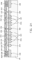
- Figure 2A shows a cross-section view of an ohmic MEMS switch according to an embodiment. This disclosure describes a method of generating a controlled landing force on the contact while allowing a large operating voltage window.
- the MEMS switch contains an RF electrode 102, pull-down electrodes 104 and anchor electrodes 108 located on substrate 101.
- the pull-down electrodes are covered with a dielectric layer 202 to avoid a short-circuit between the MEMS switch and the pull-down electrode in the pulled-down state.
- Suitable materials for the electrically insulating layer 202 include silicon based materials including silicon-oxide, silicon-dioxide, silicon-nitride and silicon-oxynitride. The thickness of this layer 202 is typically in the range of 50nm to 150nm to limit the electric field in the dielectric layer.
- the device contains additional plate-landing electrode 204 which can be unconnected (as shown) or connected to the anchor electrode 108.
- Typical materials used for the contacts 206, 208, 210 include Ti, TiN, TiAl, TiAIN, AIN, Al, W, Pt, Ir, Rh, Ru, RuO 2 , ITO and Mo and combinations thereof.
- the switch element contains a stiff bridge consisting of conductive layers 212, 214 which are joined together using an array of vias 215. This allows for a stiff plate-section and compliant legs to provide a high contact-force while keeping the operating voltage to acceptable levels.
- the MEMS bridge is suspended by legs 216 formed in the lower layer 212 and legs 218 formed in the upper layer 214 of the MEMS bridge.
- the upper layer 214 of the MEMS bridge is anchored to the lower layer 212 of the MEMS in the anchor with via 220.
- the lower layer of the MEMS bridge is anchored to the anchor contact 208 with via 222.
- Additional contact stoppers 224 are located above little islands 226 which are surrounded by the pull-down electrodes 104. When a high enough voltage is applied to the pull-down electrodes, the MEMS bridge deflects until it stops on these contact stoppers 224. The contact stoppers 224 are spaced close enough that the voltage on the pull-down electrode can be increased by a large amount without causing a substantial increase in MEMS plate displacement. The little islands 226 are electrically isolated from the pull-down electrode 104 which reduces the electric field in the contact areas 224 where they touch the MEMS-bridge.
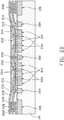
- FIG. 2B shows the ohmic MEMS device in the actuated down state.
- the MEMS bridge rests on the RF-contact 206, plate-stopper contact 210 and additional contact stoppers 224.
- the height of the contacts 206, 210 is greater than the height of the additional contact stoppers 224. This causes the MEMS bridge to flex around the RF-contact 206 which creates a large contact force. This is required for a good ohmic contact.
- the contact force (and thus also the contact resistance) can be controlled.
- a further increase in applied voltage will not substantially increase the contact force on the RF-contact 206 and thus a stable contact resistance can be obtained for a wide operating voltage range.
- the height of the additional contact stoppers 224 the remaining gap between the MEMS bridge and the dielectric above the pull-down electrode 104 can be controlled which can reduce the chance of dielectric charging.
- the contact force is set by the thickness of the contacts 206, 210 and by the thickness of the additional stoppers 224 and dielectric 202. Since all these thicknesses are controlled by deposition, a good control of the contact force can be obtained.
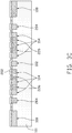
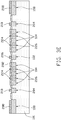
- Figure 2C shows a schematic top-view of the bottom controlled landing surface of the MEMS-switch. It shows the additional contact stoppers 224 above the isolated islands 226 which are surrounded by the pull-down electrodes 104. Because of the close-spacing between these additional stoppers 224, the MEMS plate cannot be pulled down any further once landed on these stoppers. This ensures that the dielectric surface above the pull-down electrode does not see a very high electric field which prevents dielectric charging which causes a shift in the actuation voltage.
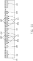
- Figures 3A-3F are schematic illustrations of the bottom controlled landing surfaces of the MEMS ohmic switch at various stages of fabrication according to one embodiment.
- Figure 3A shows the backplane starting material of the MEMS-switch and contains a substrate 101 with a plurality of electrodes including the RF electrode 102, pull-down electrodes 104, isolated islands 226, plate-landing electrode 204 and the anchor electrodes 108.
- the substrate 101 may comprise a single layer substrate or a multi-layer substrate such as a CMOS substrate having one or more layers of interconnects.
- suitable materials that may be used for these electrodes 102, 104, 226, 204, 108 include titanium-nitride, aluminum, tungsten, copper, titanium, and combinations thereof including multi-layer stacks of different material.
- Figure 3B shows the results after gap-fill with additional dielectric material (e.g. with silicon-dioxide) and CMP (chemical mechanical polishing) of the dielectric material.
- additional dielectric material e.g. with silicon-dioxide
- CMP chemical mechanical polishing
- the substrate is subsequently covered with an additional dielectric layer 202 which will protect the pull-down electrodes.
- Typical thicknesses for layer dielectric layer 202 are 50 to 150nm to limit the electric fields in this dielectric layer.
- an additional layer is deposited and patterned which will provide the additional mechanical stopper 224.
- These stoppers 224 are oversized with respect to the isolated islands 226. Because the metal surface is higher than the dielectric surface the final area that will be in contact with the landed MEMS bridge is determined by the size of the isolated islands 226.
- the choice of material for stoppers 224 is such that it can be etched with a good selectivity with respect to the underlying dielectric layer 202. For instance it could consist of a metal like Titanium, Titanium-nitride, or a dielectric like silicon-nitride and silicon-oxynitride. Typical thicknesses for stoppers 224 are 20 to 50nm.
- the RF contact 206, plate-contacts 210 and anchor contacts 208 are generated by opening a via in the dielectric layer 202 and depositing a the contact material which is subsequently patterned to form contacts 206, 208, 210.
- Typical materials used for the contacting layers 210, 206, 208 include Ti, TiN, TiAl, TiAIN, AIN, Al, W, Pt, Ir, Rh, Ru, RuO 2 , ITO and Mo and combinations thereof.
- the thickness of this layer is typically such that it protrudes above the stoppers 224 by 20 to 80nm, depending on what contact force needs to be generated.
- Figure 3F shows an alternative embodiment where the stoppers 224 is embedded inside the dielectric layer 202.
- MEMS bridge touches the dielectric layer 202 above these stoppers 224 instead of touching the stoppers 224 themselves.
- This is embedded contact layer is generated by an additional deposition of a dielectric layer 202 on top of the surface after patterning the contact stoppers 224 in Figure 3D .
- the thicknesses of the first and second part of the dielectric depositions before and after patterning stoppers 224 can be reduced.
- Figure 3G shows yet another alternative embodiment where the contact layer is patterned to form the stoppers 224 directly on top of the metal islands 226 and is subsequently covered with the dielectric layer 202.
- All three embodiments of Figure 3E , 3F and 3G give good control of the contact heights as all are relative to the top-surface of the metal electrodes 102, 104, 106 which are at the same height.
- the contact heights are set by the deposition thicknesses of layers used to form dielectric layer 202, stoppers 224 and electrodes 206, 208, 210 which can be tightly controlled in the process.
- the contact resistance of MEMS switches can be controlled over a wide voltage operating range.
Landscapes
- Engineering & Computer Science (AREA)
- Microelectronics & Electronic Packaging (AREA)
- Computer Hardware Design (AREA)
- Power Engineering (AREA)
- Micromachines (AREA)
Claims (18)
- MEMS (microelectromechanical systems)-Vorrichtung (100), Folgendes umfassend:ein Substrat (101), das wenigstens eine Ankerelektrode (108) aufweist, wobei eine HF-Elektrode (102) und eine Pull-Down-Elektrode (104) darin angeordnet sind,ein Schaltungselement (200), das über dem Substrat (101) angeordnet ist, wobei das Schaltungselement (200) elektrisch mit der Ankerelektrode (108) gekoppelt ist und von einer ersten Position, die in einer ersten Entfernung von der HF-Elektrode (102) beabstandet ist, und einer zweiten Position, die in einer zweiten Entfernung von der RF-Elektrode (102) beabstandet ist, bewegbar ist, wobei die zweite Entfernung geringer ist als die erste Entfernung;und eine dielektrische Schicht (202), die über der Pull-Down-Elektrode (104) angeordnet ist;dadurch gekennzeichnet, dass die Pull-Down-Elektrode (104) mehrere Inseln (226) aufweist, die darin angeordnet sind, wobei die mehreren Inseln (226) elektrisch isoliert sind von der Pull-Down-Elektrode (104), undKontaktstopper (224) auf der dielektrischen Schicht (202) an Stellen angeordnet sind, die den Inseln (226) entsprechen.
- MEMS-Vorrichtung (100) nach Anspruch 1, ferner Folgendes umfassend:einen Ankerkontakt (208), der auf der Ankerelektrode (108) angeordnet ist und sich zu einer ersten Höhe über dem Substrat (101) hin erstreckt; undeinen HF-Kontakt (206), der auf der HF-Elektrode (102) angeordnet ist und sich zu der ersten Höhe über dem Substrat (101) hin erstreckt.
- MEMS-Vorrichtung (100), nach Anspruch 2, wobei die Kontaktstopper (224) und die dielektrische Schicht (202) sich kollektiv zu einer zweiten Höhe über dem Substrat (101) hin erstrecken, wobei die zweite Höhe geringer ist als die erste Höhe.
- MEMS-Vorrichtung (100) nach Anspruch 1, ferner umfassend eine Plattenaufsetzelektrode (204), die in dem Substrat (101) zwischen der Ankerelektrode (108) und der Pull-Down-Elektrode (104) angeordnet ist.
- MEMS-Vorrichtung (100) nach Anspruch 4, ferner umfassend einen Plattenaufsetzkontakt (210), der auf der Plattenaufsetzelektrode (204) angeordnet ist.
- MEMS-Vorrichtung (100) nach Anspruch 5, wobei der Plattenaufsetzkontakt (210) sich über dem Substrat (101) auf der ersten Höhe erstreckt.
- MEMS-Vorrichtung (100), Folgendes umfassend:ein Substrat (101), das wenigstens eine Ankerelektrode (108) umfasst, wobei eine HF-Elektrode (102) und eine Pull-Down-Elektrode (104) darin angeordnet sind, undein Schaltungselement (200), das über dem Substrat (101) angeordnet ist, wobei das Schaltungselement (200) elektrisch mit der Ankerelektrode (108) gekoppelt ist und von einer ersten Position, die in einer ersten Entfernung von der HF-Elektrode (102) beabstandet ist, und einer zweiten Position, die in einer zweiten Entfernung von der RF-Elektrode (102) beabstandet ist, bewegbar ist, wobei die zweite Entfernung geringer ist als die erste Entfernung, dadurch gekennzeichnet, dass die Pull-Down-Elektrode (104) mehrere Inseln (226) aufweist, die darin angeordnet sind, wobei die mehreren Inseln (226) elektronisch isoliert sind von der Pull-Down-Elektrode (104), wobeiKontaktstopper (224) auf den Inseln (226) angeordnet sind, undeine dielektrische Schicht (202) über dem Substrat (101), den Kontaktstoppern (224) und der Pull-Down-Elektrode (104) angeordnet ist.
- MEMS-Vorrichtung (100) nach Anspruch 7, ferner Folgendes umfassend:einen Ankerkontakt (208), der auf der Ankerelektrode (108) angeordnet ist und sich zu einer ersten Höhe über dem Substrat (101) hin erstreckt; undeinen HF-Kontakt (206), der auf der HF-Elektrode (102) angeordnet ist und sich zu der ersten Höhe über dem Substrat (101) hin erstreckt.
- MEMS-Vorrichtung (100) nach Anspruch 8, wobei die Kontaktstopper (224) und die dielektrische Schicht (202) sich kollektiv zu einer zweiten Höhe über dem Substrat (101) hin erstrecken, wobei die zweite Höhe geringer ist als die erste Höhe.
- MEMS-Vorrichtung (100) nach Anspruch 7, ferner umfassend eine Plattenaufsetzelektrode (204), die in dem Substrat (101) zwischen der Ankerelektrode (108) und der Pull-Down-Elektrode (104) angeordnet ist.
- MEMS-Vorrichtung (100) nach Anspruch 10, ferner umfassen einen Plattenaufsetzkontakt (210), der auf der Plattenaufsetzelektrode (204) angeordnet ist.
- MEMS-Vorrichtung (100) nach Anspruch 11, wobei der Plattenaufsetzkontakt (210) sich über dem Substrat (101) auf der ersten Höhe erstreckt.
- MEMS-Vorrichtung (100), Folgendes umfassend:ein Substrat (101), das wenigstens eine Ankerelektrode (108) aufweist, wobei eine HF-Elektrode (102) und eine Pull-Down-Elektrode (104) darin angeordnet sind,ein Schaltungselement (200), das über dem Substrat (101) angeordnet ist, wobei das Schaltungselement (200) elektrisch mit der Ankerelektrode (108) gekoppelt ist und von einer ersten Position, die in einer ersten Entfernung von der HF-Elektrode (102) beabstandet ist, und einer zweiten Position, die in einer zweiten Entfernung von der RF-Elektrode (102) beabstandet ist, bewegbar ist, wobei die zweite Entfernung geringer ist als die erste Entfernung;und eine dielektrische Schicht (202), die über der Pull-Down-Elektrode (104) angeordnet ist;dadurch gekennzeichnet, dass die Pull-Down-Elektrode (104) mehrere Inseln (226) aufweist, die darin angeordnet sind, wobei die mehreren Inseln (226) elektrisch isoliert sind von der Pull-Down-Elektrode (104), undKontaktstopper (224), die innerhalb der dielektrischen Schicht (202) an Stellen angeordnet sind, die den Inseln (226) entsprechen.
- MEMS-Vorrichtung (100) nach Anspruch 13, ferner Folgendes umfassend:einen Ankerkontakt (208), der auf der Ankerelektrode (108) angeordnet ist und sich zu einer ersten Höhe über dem Substrat (101) hin erstreckt; undeinen HF-Kontakt (206), der auf der HF-Elektrode (102) angeordnet ist und sich zu der ersten Höhe über dem Substrat (101) hin erstreckt.
- MEMS-Vorrichtung (100) nach Anspruch 14, wobei die Kontaktstopper (210) und die dielektrische Schicht (202) sich kollektiv zu einer zweiten Höhe über dem Substrat (101) hin erstrecken, wobei die zweite Höhe geringer ist als die erste Höhe.
- MEMS-Vorrichtung (100) nach Anspruch 13, ferner umfassend eine Plattenaufsetzelektrode (204), die in dem Substrat (101) zwischen der Ankerelektrode (108) und der Pull-Down-Elektrode (104) angeordnet ist.
- MEMS-Vorrichtung (100) nach Anspruch 16, ferner umfassend einen Plattenaufsetzkontakt (210), der in der Plattenaufsetzelektrode (204) angeordnet ist.
- MEMS-Vorrichtung (100) nach Anspruch 17, wobei der Plattenaufsetzkontakt (210) sich über dem Substrat (101) auf der ersten Höhe erstreckt.
Applications Claiming Priority (2)
| Application Number | Priority Date | Filing Date | Title |
|---|---|---|---|
| US201562256001P | 2015-11-16 | 2015-11-16 | |
| PCT/US2016/061938 WO2017087342A1 (en) | 2015-11-16 | 2016-11-15 | Mems rf-switch with controlled contact landing |
Publications (2)
| Publication Number | Publication Date |
|---|---|
| EP3378088A1 EP3378088A1 (de) | 2018-09-26 |
| EP3378088B1 true EP3378088B1 (de) | 2019-08-21 |
Family
ID=57442818
Family Applications (1)
| Application Number | Title | Priority Date | Filing Date |
|---|---|---|---|
| EP16804971.6A Active EP3378088B1 (de) | 2015-11-16 | 2016-11-15 | Mems-rf-schalter mit gesteuerter kontaktlandung |
Country Status (6)
| Country | Link |
|---|---|
| US (1) | US10566163B2 (de) |
| EP (1) | EP3378088B1 (de) |
| JP (1) | JP6858187B2 (de) |
| KR (1) | KR102565879B1 (de) |
| CN (1) | CN108292576B (de) |
| WO (1) | WO2017087342A1 (de) |
Families Citing this family (4)
| Publication number | Priority date | Publication date | Assignee | Title |
|---|---|---|---|---|
| US11746002B2 (en) | 2019-06-22 | 2023-09-05 | Qorvo Us, Inc. | Stable landing above RF conductor in MEMS device |
| US11705298B2 (en) * | 2019-06-22 | 2023-07-18 | Qorvo Us, Inc. | Flexible MEMS device having hinged sections |
| US11667516B2 (en) | 2019-06-26 | 2023-06-06 | Qorvo Us, Inc. | MEMS device having uniform contacts |
| US20220293382A1 (en) * | 2021-03-12 | 2022-09-15 | Qorvo Us, Inc. | Mems switch with beam contact portion continuously extending between input and output terminal electrodes |
Family Cites Families (9)
| Publication number | Priority date | Publication date | Assignee | Title |
|---|---|---|---|---|
| US7101724B2 (en) * | 2004-02-20 | 2006-09-05 | Wireless Mems, Inc. | Method of fabricating semiconductor devices employing at least one modulation doped quantum well structure and one or more etch stop layers for accurate contact formation |
| JP2011011325A (ja) * | 2009-07-06 | 2011-01-20 | Murata Mfg Co Ltd | Mems素子 |
| JP5720485B2 (ja) * | 2011-08-12 | 2015-05-20 | オムロン株式会社 | 電子部品 |
| JP2013042024A (ja) * | 2011-08-18 | 2013-02-28 | Murata Mfg Co Ltd | 可変容量装置 |
| US9708177B2 (en) | 2011-09-02 | 2017-07-18 | Cavendish Kinetics, Inc. | MEMS device anchoring |
| US20130134018A1 (en) * | 2011-11-30 | 2013-05-30 | General Electric Company | Micro-electromechanical switch and a related method thereof |
| WO2013153566A1 (ja) * | 2012-04-09 | 2013-10-17 | パイオニア株式会社 | 静電アクチュエーター、可変容量コンデンサー、電気スイッチおよび静電アクチュエーターの駆動方法 |
| JP6434491B2 (ja) * | 2013-04-04 | 2018-12-05 | キャベンディッシュ・キネティックス・インコーポレイテッドCavendish Kinetics, Inc. | 高い線形性を有するmems可変デジタルキャパシタデザイン |
| JP6397913B2 (ja) * | 2013-08-01 | 2018-09-26 | キャベンディッシュ・キネティックス・インコーポレイテッドCavendish Kinetics, Inc. | Mems抵抗スイッチおよびmimキャパシタを利用したdvc |
-
2016
- 2016-11-15 JP JP2018525368A patent/JP6858187B2/ja active Active
- 2016-11-15 US US15/770,705 patent/US10566163B2/en active Active
- 2016-11-15 WO PCT/US2016/061938 patent/WO2017087342A1/en not_active Ceased
- 2016-11-15 EP EP16804971.6A patent/EP3378088B1/de active Active
- 2016-11-15 CN CN201680065979.8A patent/CN108292576B/zh active Active
- 2016-11-15 KR KR1020187016915A patent/KR102565879B1/ko active Active
Non-Patent Citations (1)
| Title |
|---|
| None * |
Also Published As
| Publication number | Publication date |
|---|---|
| KR102565879B1 (ko) | 2023-08-10 |
| JP6858187B2 (ja) | 2021-04-14 |
| CN108292576A (zh) | 2018-07-17 |
| JP2018533826A (ja) | 2018-11-15 |
| WO2017087342A1 (en) | 2017-05-26 |
| CN108292576B (zh) | 2020-06-26 |
| US20180315571A1 (en) | 2018-11-01 |
| KR20180083392A (ko) | 2018-07-20 |
| EP3378088A1 (de) | 2018-09-26 |
| US10566163B2 (en) | 2020-02-18 |
Similar Documents
| Publication | Publication Date | Title |
|---|---|---|
| JP6397913B2 (ja) | Mems抵抗スイッチおよびmimキャパシタを利用したdvc | |
| EP3378088B1 (de) | Mems-rf-schalter mit gesteuerter kontaktlandung | |
| EP3378087B1 (de) | Natürlich geschlossener mems-schalter für schutz vor elektrostatischer entladung | |
| EP3520129B1 (de) | Mems-rf-schalter mit aufpralllandung nahe null | |
| EP3378080B1 (de) | Mems-vorrichtung und verfahren zur herstellung einer mems-vorrichtung | |
| JP6858186B2 (ja) | 高出力rf memsスイッチでの熱管理 | |
| EP3378086B1 (de) | Stromhandhabung in beinen und anker eines hf-schalters | |
| EP3254294B1 (de) | Dvc mit verwendung von mims im anker |
Legal Events
| Date | Code | Title | Description |
|---|---|---|---|
| STAA | Information on the status of an ep patent application or granted ep patent |
Free format text: STATUS: UNKNOWN |
|
| STAA | Information on the status of an ep patent application or granted ep patent |
Free format text: STATUS: THE INTERNATIONAL PUBLICATION HAS BEEN MADE |
|
| PUAI | Public reference made under article 153(3) epc to a published international application that has entered the european phase |
Free format text: ORIGINAL CODE: 0009012 |
|
| STAA | Information on the status of an ep patent application or granted ep patent |
Free format text: STATUS: REQUEST FOR EXAMINATION WAS MADE |
|
| 17P | Request for examination filed |
Effective date: 20180426 |
|
| AK | Designated contracting states |
Kind code of ref document: A1 Designated state(s): AL AT BE BG CH CY CZ DE DK EE ES FI FR GB GR HR HU IE IS IT LI LT LU LV MC MK MT NL NO PL PT RO RS SE SI SK SM TR |
|
| AX | Request for extension of the european patent |
Extension state: BA ME |
|
| DAV | Request for validation of the european patent (deleted) | ||
| DAX | Request for extension of the european patent (deleted) | ||
| GRAP | Despatch of communication of intention to grant a patent |
Free format text: ORIGINAL CODE: EPIDOSNIGR1 |
|
| STAA | Information on the status of an ep patent application or granted ep patent |
Free format text: STATUS: GRANT OF PATENT IS INTENDED |
|
| INTG | Intention to grant announced |
Effective date: 20190318 |
|
| GRAS | Grant fee paid |
Free format text: ORIGINAL CODE: EPIDOSNIGR3 |
|
| GRAA | (expected) grant |
Free format text: ORIGINAL CODE: 0009210 |
|
| STAA | Information on the status of an ep patent application or granted ep patent |
Free format text: STATUS: THE PATENT HAS BEEN GRANTED |
|
| AK | Designated contracting states |
Kind code of ref document: B1 Designated state(s): AL AT BE BG CH CY CZ DE DK EE ES FI FR GB GR HR HU IE IS IT LI LT LU LV MC MK MT NL NO PL PT RO RS SE SI SK SM TR |
|
| REG | Reference to a national code |
Ref country code: GB Ref legal event code: FG4D |
|
| REG | Reference to a national code |
Ref country code: CH Ref legal event code: EP |
|
| REG | Reference to a national code |
Ref country code: DE Ref legal event code: R096 Ref document number: 602016019164 Country of ref document: DE |
|
| REG | Reference to a national code |
Ref country code: AT Ref legal event code: REF Ref document number: 1170705 Country of ref document: AT Kind code of ref document: T Effective date: 20190915 |
|
| REG | Reference to a national code |
Ref country code: IE Ref legal event code: FG4D |
|
| REG | Reference to a national code |
Ref country code: LT Ref legal event code: MG4D |
|
| REG | Reference to a national code |
Ref country code: NL Ref legal event code: MP Effective date: 20190821 |
|
| PG25 | Lapsed in a contracting state [announced via postgrant information from national office to epo] |
Ref country code: NO Free format text: LAPSE BECAUSE OF FAILURE TO SUBMIT A TRANSLATION OF THE DESCRIPTION OR TO PAY THE FEE WITHIN THE PRESCRIBED TIME-LIMIT Effective date: 20191121 Ref country code: PT Free format text: LAPSE BECAUSE OF FAILURE TO SUBMIT A TRANSLATION OF THE DESCRIPTION OR TO PAY THE FEE WITHIN THE PRESCRIBED TIME-LIMIT Effective date: 20191223 Ref country code: LT Free format text: LAPSE BECAUSE OF FAILURE TO SUBMIT A TRANSLATION OF THE DESCRIPTION OR TO PAY THE FEE WITHIN THE PRESCRIBED TIME-LIMIT Effective date: 20190821 Ref country code: NL Free format text: LAPSE BECAUSE OF FAILURE TO SUBMIT A TRANSLATION OF THE DESCRIPTION OR TO PAY THE FEE WITHIN THE PRESCRIBED TIME-LIMIT Effective date: 20190821 Ref country code: BG Free format text: LAPSE BECAUSE OF FAILURE TO SUBMIT A TRANSLATION OF THE DESCRIPTION OR TO PAY THE FEE WITHIN THE PRESCRIBED TIME-LIMIT Effective date: 20191121 Ref country code: FI Free format text: LAPSE BECAUSE OF FAILURE TO SUBMIT A TRANSLATION OF THE DESCRIPTION OR TO PAY THE FEE WITHIN THE PRESCRIBED TIME-LIMIT Effective date: 20190821 Ref country code: HR Free format text: LAPSE BECAUSE OF FAILURE TO SUBMIT A TRANSLATION OF THE DESCRIPTION OR TO PAY THE FEE WITHIN THE PRESCRIBED TIME-LIMIT Effective date: 20190821 Ref country code: SE Free format text: LAPSE BECAUSE OF FAILURE TO SUBMIT A TRANSLATION OF THE DESCRIPTION OR TO PAY THE FEE WITHIN THE PRESCRIBED TIME-LIMIT Effective date: 20190821 |
|
| PG25 | Lapsed in a contracting state [announced via postgrant information from national office to epo] |
Ref country code: ES Free format text: LAPSE BECAUSE OF FAILURE TO SUBMIT A TRANSLATION OF THE DESCRIPTION OR TO PAY THE FEE WITHIN THE PRESCRIBED TIME-LIMIT Effective date: 20190821 Ref country code: GR Free format text: LAPSE BECAUSE OF FAILURE TO SUBMIT A TRANSLATION OF THE DESCRIPTION OR TO PAY THE FEE WITHIN THE PRESCRIBED TIME-LIMIT Effective date: 20191122 Ref country code: LV Free format text: LAPSE BECAUSE OF FAILURE TO SUBMIT A TRANSLATION OF THE DESCRIPTION OR TO PAY THE FEE WITHIN THE PRESCRIBED TIME-LIMIT Effective date: 20190821 Ref country code: AL Free format text: LAPSE BECAUSE OF FAILURE TO SUBMIT A TRANSLATION OF THE DESCRIPTION OR TO PAY THE FEE WITHIN THE PRESCRIBED TIME-LIMIT Effective date: 20190821 Ref country code: RS Free format text: LAPSE BECAUSE OF FAILURE TO SUBMIT A TRANSLATION OF THE DESCRIPTION OR TO PAY THE FEE WITHIN THE PRESCRIBED TIME-LIMIT Effective date: 20190821 Ref country code: IS Free format text: LAPSE BECAUSE OF FAILURE TO SUBMIT A TRANSLATION OF THE DESCRIPTION OR TO PAY THE FEE WITHIN THE PRESCRIBED TIME-LIMIT Effective date: 20191221 |
|
| REG | Reference to a national code |
Ref country code: AT Ref legal event code: MK05 Ref document number: 1170705 Country of ref document: AT Kind code of ref document: T Effective date: 20190821 |
|
| PG25 | Lapsed in a contracting state [announced via postgrant information from national office to epo] |
Ref country code: TR Free format text: LAPSE BECAUSE OF FAILURE TO SUBMIT A TRANSLATION OF THE DESCRIPTION OR TO PAY THE FEE WITHIN THE PRESCRIBED TIME-LIMIT Effective date: 20190821 |
|
| PG25 | Lapsed in a contracting state [announced via postgrant information from national office to epo] |
Ref country code: IT Free format text: LAPSE BECAUSE OF FAILURE TO SUBMIT A TRANSLATION OF THE DESCRIPTION OR TO PAY THE FEE WITHIN THE PRESCRIBED TIME-LIMIT Effective date: 20190821 Ref country code: AT Free format text: LAPSE BECAUSE OF FAILURE TO SUBMIT A TRANSLATION OF THE DESCRIPTION OR TO PAY THE FEE WITHIN THE PRESCRIBED TIME-LIMIT Effective date: 20190821 Ref country code: DK Free format text: LAPSE BECAUSE OF FAILURE TO SUBMIT A TRANSLATION OF THE DESCRIPTION OR TO PAY THE FEE WITHIN THE PRESCRIBED TIME-LIMIT Effective date: 20190821 Ref country code: EE Free format text: LAPSE BECAUSE OF FAILURE TO SUBMIT A TRANSLATION OF THE DESCRIPTION OR TO PAY THE FEE WITHIN THE PRESCRIBED TIME-LIMIT Effective date: 20190821 Ref country code: RO Free format text: LAPSE BECAUSE OF FAILURE TO SUBMIT A TRANSLATION OF THE DESCRIPTION OR TO PAY THE FEE WITHIN THE PRESCRIBED TIME-LIMIT Effective date: 20190821 Ref country code: PL Free format text: LAPSE BECAUSE OF FAILURE TO SUBMIT A TRANSLATION OF THE DESCRIPTION OR TO PAY THE FEE WITHIN THE PRESCRIBED TIME-LIMIT Effective date: 20190821 |
|
| PG25 | Lapsed in a contracting state [announced via postgrant information from national office to epo] |
Ref country code: IS Free format text: LAPSE BECAUSE OF FAILURE TO SUBMIT A TRANSLATION OF THE DESCRIPTION OR TO PAY THE FEE WITHIN THE PRESCRIBED TIME-LIMIT Effective date: 20200224 Ref country code: SK Free format text: LAPSE BECAUSE OF FAILURE TO SUBMIT A TRANSLATION OF THE DESCRIPTION OR TO PAY THE FEE WITHIN THE PRESCRIBED TIME-LIMIT Effective date: 20190821 Ref country code: CZ Free format text: LAPSE BECAUSE OF FAILURE TO SUBMIT A TRANSLATION OF THE DESCRIPTION OR TO PAY THE FEE WITHIN THE PRESCRIBED TIME-LIMIT Effective date: 20190821 Ref country code: SM Free format text: LAPSE BECAUSE OF FAILURE TO SUBMIT A TRANSLATION OF THE DESCRIPTION OR TO PAY THE FEE WITHIN THE PRESCRIBED TIME-LIMIT Effective date: 20190821 |
|
| REG | Reference to a national code |
Ref country code: DE Ref legal event code: R097 Ref document number: 602016019164 Country of ref document: DE |
|
| REG | Reference to a national code |
Ref country code: CH Ref legal event code: PL |
|
| PLBE | No opposition filed within time limit |
Free format text: ORIGINAL CODE: 0009261 |
|
| STAA | Information on the status of an ep patent application or granted ep patent |
Free format text: STATUS: NO OPPOSITION FILED WITHIN TIME LIMIT |
|
| PG2D | Information on lapse in contracting state deleted |
Ref country code: IS |
|
| PG25 | Lapsed in a contracting state [announced via postgrant information from national office to epo] |
Ref country code: LU Free format text: LAPSE BECAUSE OF NON-PAYMENT OF DUE FEES Effective date: 20191115 Ref country code: MC Free format text: LAPSE BECAUSE OF FAILURE TO SUBMIT A TRANSLATION OF THE DESCRIPTION OR TO PAY THE FEE WITHIN THE PRESCRIBED TIME-LIMIT Effective date: 20190821 Ref country code: CH Free format text: LAPSE BECAUSE OF NON-PAYMENT OF DUE FEES Effective date: 20191130 Ref country code: LI Free format text: LAPSE BECAUSE OF NON-PAYMENT OF DUE FEES Effective date: 20191130 |
|
| 26N | No opposition filed |
Effective date: 20200603 |
|
| REG | Reference to a national code |
Ref country code: BE Ref legal event code: MM Effective date: 20191130 |
|
| PG25 | Lapsed in a contracting state [announced via postgrant information from national office to epo] |
Ref country code: SI Free format text: LAPSE BECAUSE OF FAILURE TO SUBMIT A TRANSLATION OF THE DESCRIPTION OR TO PAY THE FEE WITHIN THE PRESCRIBED TIME-LIMIT Effective date: 20190821 |
|
| PG25 | Lapsed in a contracting state [announced via postgrant information from national office to epo] |
Ref country code: IE Free format text: LAPSE BECAUSE OF NON-PAYMENT OF DUE FEES Effective date: 20191115 |
|
| PG25 | Lapsed in a contracting state [announced via postgrant information from national office to epo] |
Ref country code: BE Free format text: LAPSE BECAUSE OF NON-PAYMENT OF DUE FEES Effective date: 20191130 |
|
| PG25 | Lapsed in a contracting state [announced via postgrant information from national office to epo] |
Ref country code: CY Free format text: LAPSE BECAUSE OF FAILURE TO SUBMIT A TRANSLATION OF THE DESCRIPTION OR TO PAY THE FEE WITHIN THE PRESCRIBED TIME-LIMIT Effective date: 20190821 |
|
| PG25 | Lapsed in a contracting state [announced via postgrant information from national office to epo] |
Ref country code: HU Free format text: LAPSE BECAUSE OF FAILURE TO SUBMIT A TRANSLATION OF THE DESCRIPTION OR TO PAY THE FEE WITHIN THE PRESCRIBED TIME-LIMIT; INVALID AB INITIO Effective date: 20161115 Ref country code: MT Free format text: LAPSE BECAUSE OF FAILURE TO SUBMIT A TRANSLATION OF THE DESCRIPTION OR TO PAY THE FEE WITHIN THE PRESCRIBED TIME-LIMIT Effective date: 20190821 |
|
| REG | Reference to a national code |
Ref country code: GB Ref legal event code: 732E Free format text: REGISTERED BETWEEN 20220505 AND 20220512 |
|
| PG25 | Lapsed in a contracting state [announced via postgrant information from national office to epo] |
Ref country code: MK Free format text: LAPSE BECAUSE OF FAILURE TO SUBMIT A TRANSLATION OF THE DESCRIPTION OR TO PAY THE FEE WITHIN THE PRESCRIBED TIME-LIMIT Effective date: 20190821 |
|
| REG | Reference to a national code |
Ref country code: DE Ref legal event code: R081 Ref document number: 602016019164 Country of ref document: DE Owner name: QORVO US, INC., GREENSBORO, US Free format text: FORMER OWNER: CAVENDISH KINETICS INC., SAN JOSE, CALIF., US |
|
| PGFP | Annual fee paid to national office [announced via postgrant information from national office to epo] |
Ref country code: DE Payment date: 20251022 Year of fee payment: 10 |
|
| PGFP | Annual fee paid to national office [announced via postgrant information from national office to epo] |
Ref country code: GB Payment date: 20251023 Year of fee payment: 10 |
|
| PGFP | Annual fee paid to national office [announced via postgrant information from national office to epo] |
Ref country code: FR Payment date: 20251023 Year of fee payment: 10 |