EP2831708B1 - Corps transparent destiné à être utilisé dans un panneau tactile et son procédé de fabrication et appareil - Google Patents
Corps transparent destiné à être utilisé dans un panneau tactile et son procédé de fabrication et appareil Download PDFInfo
- Publication number
- EP2831708B1 EP2831708B1 EP12711408.0A EP12711408A EP2831708B1 EP 2831708 B1 EP2831708 B1 EP 2831708B1 EP 12711408 A EP12711408 A EP 12711408A EP 2831708 B1 EP2831708 B1 EP 2831708B1
- Authority
- EP
- European Patent Office
- Prior art keywords
- transparent
- refractive index
- layer stack
- dielectric film
- transparent conductive
- Prior art date
- Legal status (The legal status is an assumption and is not a legal conclusion. Google has not performed a legal analysis and makes no representation as to the accuracy of the status listed.)
- Active
Links
- 238000004519 manufacturing process Methods 0.000 title claims description 25
- 239000000758 substrate Substances 0.000 claims description 93
- 238000000151 deposition Methods 0.000 claims description 76
- 230000008021 deposition Effects 0.000 claims description 58
- 238000004544 sputter deposition Methods 0.000 claims description 38
- 238000000034 method Methods 0.000 claims description 35
- 239000000853 adhesive Substances 0.000 claims description 29
- 230000001070 adhesive effect Effects 0.000 claims description 29
- VYPSYNLAJGMNEJ-UHFFFAOYSA-N Silicium dioxide Chemical compound O=[Si]=O VYPSYNLAJGMNEJ-UHFFFAOYSA-N 0.000 claims description 25
- 230000008569 process Effects 0.000 claims description 23
- 239000011521 glass Substances 0.000 claims description 14
- 229910020286 SiOxNy Inorganic materials 0.000 claims description 8
- 239000000463 material Substances 0.000 claims description 8
- 238000001755 magnetron sputter deposition Methods 0.000 claims description 7
- 238000000059 patterning Methods 0.000 claims description 7
- 229910004205 SiNX Inorganic materials 0.000 claims description 5
- 229910003070 TaOx Inorganic materials 0.000 claims description 5
- 229910003087 TiOx Inorganic materials 0.000 claims description 5
- 229910052814 silicon oxide Inorganic materials 0.000 claims description 5
- HLLICFJUWSZHRJ-UHFFFAOYSA-N tioxidazole Chemical compound CCCOC1=CC=C2N=C(NC(=O)OC)SC2=C1 HLLICFJUWSZHRJ-UHFFFAOYSA-N 0.000 claims description 5
- 229910017107 AlOx Inorganic materials 0.000 claims description 4
- 229910017105 AlOxNy Inorganic materials 0.000 claims description 4
- 239000011888 foil Substances 0.000 claims description 3
- AMGQUBHHOARCQH-UHFFFAOYSA-N indium;oxotin Chemical compound [In].[Sn]=O AMGQUBHHOARCQH-UHFFFAOYSA-N 0.000 claims description 3
- 239000004033 plastic Substances 0.000 claims description 3
- 229920003023 plastic Polymers 0.000 claims description 3
- 239000010410 layer Substances 0.000 description 246
- 239000010408 film Substances 0.000 description 146
- 230000003287 optical effect Effects 0.000 description 22
- ZKATWMILCYLAPD-UHFFFAOYSA-N niobium pentoxide Chemical compound O=[Nb](=O)O[Nb](=O)=O ZKATWMILCYLAPD-UHFFFAOYSA-N 0.000 description 18
- 230000005540 biological transmission Effects 0.000 description 13
- XOLBLPGZBRYERU-UHFFFAOYSA-N tin dioxide Chemical compound O=[Sn]=O XOLBLPGZBRYERU-UHFFFAOYSA-N 0.000 description 12
- 229910052681 coesite Inorganic materials 0.000 description 10
- 229910052906 cristobalite Inorganic materials 0.000 description 10
- 239000000377 silicon dioxide Substances 0.000 description 10
- 229910052682 stishovite Inorganic materials 0.000 description 10
- 229910052905 tridymite Inorganic materials 0.000 description 10
- XLOMVQKBTHCTTD-UHFFFAOYSA-N zinc oxide Inorganic materials [Zn]=O XLOMVQKBTHCTTD-UHFFFAOYSA-N 0.000 description 10
- 230000000007 visual effect Effects 0.000 description 9
- PJXISJQVUVHSOJ-UHFFFAOYSA-N indium(III) oxide Inorganic materials [O-2].[O-2].[O-2].[In+3].[In+3] PJXISJQVUVHSOJ-UHFFFAOYSA-N 0.000 description 8
- 230000008859 change Effects 0.000 description 7
- 239000002184 metal Substances 0.000 description 7
- 229910052751 metal Inorganic materials 0.000 description 7
- IJGRMHOSHXDMSA-UHFFFAOYSA-N Atomic nitrogen Chemical compound N#N IJGRMHOSHXDMSA-UHFFFAOYSA-N 0.000 description 6
- XUIMIQQOPSSXEZ-UHFFFAOYSA-N Silicon Chemical compound [Si] XUIMIQQOPSSXEZ-UHFFFAOYSA-N 0.000 description 5
- QVGXLLKOCUKJST-UHFFFAOYSA-N atomic oxygen Chemical compound [O] QVGXLLKOCUKJST-UHFFFAOYSA-N 0.000 description 5
- 230000004888 barrier function Effects 0.000 description 5
- 238000005229 chemical vapour deposition Methods 0.000 description 5
- 239000007789 gas Substances 0.000 description 5
- 239000001301 oxygen Substances 0.000 description 5
- 229910052760 oxygen Inorganic materials 0.000 description 5
- 229910052710 silicon Inorganic materials 0.000 description 5
- 239000010703 silicon Substances 0.000 description 5
- QGZKDVFQNNGYKY-UHFFFAOYSA-N Ammonia Chemical compound N QGZKDVFQNNGYKY-UHFFFAOYSA-N 0.000 description 4
- XKRFYHLGVUSROY-UHFFFAOYSA-N Argon Chemical compound [Ar] XKRFYHLGVUSROY-UHFFFAOYSA-N 0.000 description 4
- 239000012298 atmosphere Substances 0.000 description 4
- 230000005693 optoelectronics Effects 0.000 description 4
- 238000005240 physical vapour deposition Methods 0.000 description 4
- 239000000969 carrier Substances 0.000 description 3
- 238000005137 deposition process Methods 0.000 description 3
- 238000013461 design Methods 0.000 description 3
- 238000001704 evaporation Methods 0.000 description 3
- 230000008020 evaporation Effects 0.000 description 3
- 239000011810 insulating material Substances 0.000 description 3
- 239000000203 mixture Substances 0.000 description 3
- 229910052757 nitrogen Inorganic materials 0.000 description 3
- 239000002245 particle Substances 0.000 description 3
- 238000002203 pretreatment Methods 0.000 description 3
- 239000010409 thin film Substances 0.000 description 3
- 238000002834 transmittance Methods 0.000 description 3
- 229910052581 Si3N4 Inorganic materials 0.000 description 2
- 229910052786 argon Inorganic materials 0.000 description 2
- 230000000712 assembly Effects 0.000 description 2
- 238000000429 assembly Methods 0.000 description 2
- 230000015572 biosynthetic process Effects 0.000 description 2
- CXKCTMHTOKXKQT-UHFFFAOYSA-N cadmium oxide Inorganic materials [Cd]=O CXKCTMHTOKXKQT-UHFFFAOYSA-N 0.000 description 2
- 239000000919 ceramic Substances 0.000 description 2
- 239000004020 conductor Substances 0.000 description 2
- 239000006185 dispersion Substances 0.000 description 2
- 230000005611 electricity Effects 0.000 description 2
- 238000005516 engineering process Methods 0.000 description 2
- 238000010438 heat treatment Methods 0.000 description 2
- 230000006872 improvement Effects 0.000 description 2
- 238000012986 modification Methods 0.000 description 2
- 230000004048 modification Effects 0.000 description 2
- 230000007935 neutral effect Effects 0.000 description 2
- 150000004767 nitrides Chemical class 0.000 description 2
- 229920002120 photoresistant polymer Polymers 0.000 description 2
- -1 that is Substances 0.000 description 2
- 238000001429 visible spectrum Methods 0.000 description 2
- 241001163455 Eulepidotis superior Species 0.000 description 1
- UFHFLCQGNIYNRP-UHFFFAOYSA-N Hydrogen Chemical compound [H][H] UFHFLCQGNIYNRP-UHFFFAOYSA-N 0.000 description 1
- CBENFWSGALASAD-UHFFFAOYSA-N Ozone Chemical compound [O-][O+]=O CBENFWSGALASAD-UHFFFAOYSA-N 0.000 description 1
- 229910021529 ammonia Inorganic materials 0.000 description 1
- 238000000137 annealing Methods 0.000 description 1
- 239000011248 coating agent Substances 0.000 description 1
- 238000000576 coating method Methods 0.000 description 1
- 230000001010 compromised effect Effects 0.000 description 1
- 239000000356 contaminant Substances 0.000 description 1
- 238000011109 contamination Methods 0.000 description 1
- 239000012792 core layer Substances 0.000 description 1
- 239000006059 cover glass Substances 0.000 description 1
- 239000013078 crystal Substances 0.000 description 1
- 230000003247 decreasing effect Effects 0.000 description 1
- 230000007547 defect Effects 0.000 description 1
- 238000007872 degassing Methods 0.000 description 1
- 230000001419 dependent effect Effects 0.000 description 1
- 239000003574 free electron Substances 0.000 description 1
- 239000001257 hydrogen Substances 0.000 description 1
- 229910052739 hydrogen Inorganic materials 0.000 description 1
- 239000011261 inert gas Substances 0.000 description 1
- 239000007788 liquid Substances 0.000 description 1
- 239000004973 liquid crystal related substance Substances 0.000 description 1
- 229910001635 magnesium fluoride Inorganic materials 0.000 description 1
- 238000005259 measurement Methods 0.000 description 1
- 229910000484 niobium oxide Inorganic materials 0.000 description 1
- URLJKFSTXLNXLG-UHFFFAOYSA-N niobium(5+);oxygen(2-) Chemical compound [O-2].[O-2].[O-2].[O-2].[O-2].[Nb+5].[Nb+5] URLJKFSTXLNXLG-UHFFFAOYSA-N 0.000 description 1
- 239000003921 oil Substances 0.000 description 1
- 238000002161 passivation Methods 0.000 description 1
- 238000000206 photolithography Methods 0.000 description 1
- 229920003229 poly(methyl methacrylate) Polymers 0.000 description 1
- 239000004926 polymethyl methacrylate Substances 0.000 description 1
- 238000007639 printing Methods 0.000 description 1
- 238000012545 processing Methods 0.000 description 1
- 238000004549 pulsed laser deposition Methods 0.000 description 1
- 238000005546 reactive sputtering Methods 0.000 description 1
- 229910052594 sapphire Inorganic materials 0.000 description 1
- 239000010980 sapphire Substances 0.000 description 1
- 239000002904 solvent Substances 0.000 description 1
- 238000001179 sorption measurement Methods 0.000 description 1
- 239000000126 substance Substances 0.000 description 1
- 239000013077 target material Substances 0.000 description 1
- 238000012360 testing method Methods 0.000 description 1
Images


Classifications
-
- G—PHYSICS
- G02—OPTICS
- G02B—OPTICAL ELEMENTS, SYSTEMS OR APPARATUS
- G02B1/00—Optical elements characterised by the material of which they are made; Optical coatings for optical elements
- G02B1/10—Optical coatings produced by application to, or surface treatment of, optical elements
- G02B1/11—Anti-reflection coatings
- G02B1/113—Anti-reflection coatings using inorganic layer materials only
- G02B1/115—Multilayers
- G02B1/116—Multilayers including electrically conducting layers
-
- G—PHYSICS
- G06—COMPUTING; CALCULATING OR COUNTING
- G06F—ELECTRIC DIGITAL DATA PROCESSING
- G06F3/00—Input arrangements for transferring data to be processed into a form capable of being handled by the computer; Output arrangements for transferring data from processing unit to output unit, e.g. interface arrangements
- G06F3/01—Input arrangements or combined input and output arrangements for interaction between user and computer
- G06F3/03—Arrangements for converting the position or the displacement of a member into a coded form
- G06F3/041—Digitisers, e.g. for touch screens or touch pads, characterised by the transducing means
-
- C—CHEMISTRY; METALLURGY
- C23—COATING METALLIC MATERIAL; COATING MATERIAL WITH METALLIC MATERIAL; CHEMICAL SURFACE TREATMENT; DIFFUSION TREATMENT OF METALLIC MATERIAL; COATING BY VACUUM EVAPORATION, BY SPUTTERING, BY ION IMPLANTATION OR BY CHEMICAL VAPOUR DEPOSITION, IN GENERAL; INHIBITING CORROSION OF METALLIC MATERIAL OR INCRUSTATION IN GENERAL
- C23C—COATING METALLIC MATERIAL; COATING MATERIAL WITH METALLIC MATERIAL; SURFACE TREATMENT OF METALLIC MATERIAL BY DIFFUSION INTO THE SURFACE, BY CHEMICAL CONVERSION OR SUBSTITUTION; COATING BY VACUUM EVAPORATION, BY SPUTTERING, BY ION IMPLANTATION OR BY CHEMICAL VAPOUR DEPOSITION, IN GENERAL
- C23C14/00—Coating by vacuum evaporation, by sputtering or by ion implantation of the coating forming material
- C23C14/22—Coating by vacuum evaporation, by sputtering or by ion implantation of the coating forming material characterised by the process of coating
- C23C14/34—Sputtering
- C23C14/35—Sputtering by application of a magnetic field, e.g. magnetron sputtering
- C23C14/352—Sputtering by application of a magnetic field, e.g. magnetron sputtering using more than one target
-
- G—PHYSICS
- G02—OPTICS
- G02B—OPTICAL ELEMENTS, SYSTEMS OR APPARATUS
- G02B1/00—Optical elements characterised by the material of which they are made; Optical coatings for optical elements
- G02B1/10—Optical coatings produced by application to, or surface treatment of, optical elements
- G02B1/14—Protective coatings, e.g. hard coatings
-
- H—ELECTRICITY
- H01—ELECTRIC ELEMENTS
- H01J—ELECTRIC DISCHARGE TUBES OR DISCHARGE LAMPS
- H01J37/00—Discharge tubes with provision for introducing objects or material to be exposed to the discharge, e.g. for the purpose of examination or processing thereof
- H01J37/32—Gas-filled discharge tubes
- H01J37/34—Gas-filled discharge tubes operating with cathodic sputtering
- H01J37/3402—Gas-filled discharge tubes operating with cathodic sputtering using supplementary magnetic fields
- H01J37/3405—Magnetron sputtering
-
- H—ELECTRICITY
- H01—ELECTRIC ELEMENTS
- H01J—ELECTRIC DISCHARGE TUBES OR DISCHARGE LAMPS
- H01J37/00—Discharge tubes with provision for introducing objects or material to be exposed to the discharge, e.g. for the purpose of examination or processing thereof
- H01J37/32—Gas-filled discharge tubes
- H01J37/34—Gas-filled discharge tubes operating with cathodic sputtering
- H01J37/3411—Constructional aspects of the reactor
- H01J37/3414—Targets
- H01J37/3426—Material
- H01J37/3429—Plural materials
-
- G—PHYSICS
- G02—OPTICS
- G02B—OPTICAL ELEMENTS, SYSTEMS OR APPARATUS
- G02B1/00—Optical elements characterised by the material of which they are made; Optical coatings for optical elements
- G02B1/10—Optical coatings produced by application to, or surface treatment of, optical elements
- G02B1/11—Anti-reflection coatings
- G02B1/113—Anti-reflection coatings using inorganic layer materials only
- G02B1/115—Multilayers
-
- G—PHYSICS
- G02—OPTICS
- G02B—OPTICAL ELEMENTS, SYSTEMS OR APPARATUS
- G02B5/00—Optical elements other than lenses
- G02B5/20—Filters
- G02B5/28—Interference filters
- G02B5/285—Interference filters comprising deposited thin solid films
-
- G—PHYSICS
- G06—COMPUTING; CALCULATING OR COUNTING
- G06F—ELECTRIC DIGITAL DATA PROCESSING
- G06F2203/00—Indexing scheme relating to G06F3/00 - G06F3/048
- G06F2203/041—Indexing scheme relating to G06F3/041 - G06F3/045
- G06F2203/04103—Manufacturing, i.e. details related to manufacturing processes specially suited for touch sensitive devices
-
- H—ELECTRICITY
- H01—ELECTRIC ELEMENTS
- H01J—ELECTRIC DISCHARGE TUBES OR DISCHARGE LAMPS
- H01J2237/00—Discharge tubes exposing object to beam, e.g. for analysis treatment, etching, imaging
- H01J2237/32—Processing objects by plasma generation
- H01J2237/33—Processing objects by plasma generation characterised by the type of processing
- H01J2237/332—Coating
Definitions
- Embodiments of the present disclosure relate to processes and systems for manufacturing a transparent body for use in a touch panel and a transparent body fabricated according to these processes.
- Touch panels are a particular class of electronic visual displays, which are able to detect and locate a touch within a display area.
- touch panels include a transparent body disposed over a screen and configured to sense a touch. Such a body is substantially transparent, so that light in the visible spectrum emitted by the screen can be transmitted therethrough.
- At least some known touch panels include a transparent body constituted by a barrier and a transparent conductor formed, in this order, over a substrate.
- a touch on the display area of such a panel generally results in a measurable change of capacitance in a region of the transparent body. The change in capacitance may be measured using different technologies, so that the position of the touch can be determined.
- a transparent body for use with a touch panel is subject to some particular requirements.
- one key requirement is that the transparent body is stable enough for withstanding multiple contacts on the screen and harsh conditions, so that reliability of the touch screen is not compromised over time.
- at least some known transparent bodies included in touch screens, which are considered robust interfere with a proper transmission of light therethrough due to, for example, thickness, composition, and structure of the layers forming the transparent body.
- fabricating such a stable transparent body with high quality, for example with a uniform and defect-free barrier is challenging.
- transparent bodies for touch panels there are different types of transparent bodies for touch panels. Particular consideration of the optical characteristics, e.g. the appearance to a user, has to be taken into account for transparent bodies, wherein the conductive layer for measuring the change in capacitance is a structured conductive layer.
- a further aspect to be considered is the steadily increasing size of displays, wherein beyond the optical characteristics described above, also electrically characteristics are of increasing interest.
- a design of thin film based flat panel displays and touch screen technologies which provides an invisible object, which is patterned with respect to conductivity (like a touch sensor structure) and which exhibits enhanced optical and electrical performance compared to conventional structures, is desired.
- EP2402481A1 and EP1574882A1 describe methods of manufacturing touch screen panels.
- the invention provides a process according to independent claim 1, a transparent body according to independent claim 7, and an apparatus according to independent claim 15. Further aspects, advantages, and features of the present invention are apparent from the dependent claims, the description, and the accompanying drawings.
- a process for manufacturing a transparent body for use in a touch panel includes optionally depositing a first transparent layer stack over a transparent substrate, wherein said first transparent layer stack includes at least a first dielectric film with a first refractive index, and a second dielectric film with a second refractive index different from the first refractive index.
- the process includes; depositing a structured transparent conductive film over the first transparent layer stack, wherein the structured transparent conductive film corresponding to a sheet resistance of 100 Ohm/square or below; depositing a second transparent layer stack over the transparent conductive film, wherein said second transparent layer stack includes at least a third dielectric film with a third refractive index, and a fourth dielectric film with a fourth refractive index different from the third refractive index, wherein the first transparent layer stack if provided, the structured transparent conductive film and the second transparent layer stack are provided in this order.
- a transparent adhesive having a fourth refractive index different from the third refractive index can be provided instead of the fourth dielectric film.
- a transparent body adapted for use in a touch panel includes a transparent substrate, and optionally a first transparent layer stack deposited over the transparent substrate, wherein said transparent layer stack includes at least a first dielectric film with a first refractive index, and a second dielectric film with a second refractive index different from the first refractive index.
- the layer stack includes a transparent conductive film deposited over the first transparent layer stack, wherein the structured transparent conductive film has a sheet resistance of 100 Ohm/square or below, and a second transparent layer stack deposited over the transparent conductive film, wherein said second transparent layer stack includes at least a third dielectric film with a third refractive index, and a fourth dielectric film with a fourth refractive index different from the third refractive index.
- a transparent adhesive having a fourth refractive index different from the third refractive index can be provided instead of the fourth dielectric film.
- a deposition apparatus for manufacturing a transparent body for use in a touch panel.
- the apparatus includes a first deposition assembly configured to deposit a first transparent layer stack over a substrate, said first transparent layer stack including at least first dielectric film with a first refractive index, and a second dielectric film with a second refractive index different from the first refractive index, a second deposition assembly configured to deposit a transparent conductive film, and a third deposition assembly configured to deposit a second transparent layer stack over the transparent conductive film, said second transparent layer stack including at least third dielectric film with a third refractive index, and a fourth dielectric film with a fourth refractive index different from the third refractive index, wherein said first deposition assembly, said second deposition assembly, and the third deposition assembly are arranged such that the first transparent layer stack, the transparent conductive film and the second transparent layer stack are disposed over the substrate in this order, and wherein at least one of the first deposition assembly or the second deposition assembly or the third deposition assembly in
- the combination of dielectric films deposited according to embodiments of the present disclosure having additional dielectric films in comparison to at least some known transparent bodies for use in a touch panel, with a characteristic combination of refractive indexes in combination with second transparent layer stack of dielectric films, and in which at least one of the films is deposited by sputtering of a target facilitates manufacturing of a high-quality transparent body that not only yields proper transmission of light but also yields stable performance over time.
- the resistance can be reduced, which is, for example, useful for large area touch panels.
- Embodiments are also directed to apparatuses for carrying out the disclosed processes and including apparatus parts for performing described process steps. Furthermore, embodiments are also directed to methods by which the described apparatus operates or by which the described apparatus is manufactured. The methods may include method steps for carrying out functions of the apparatus or manufacturing parts of the apparatus. The method steps may be performed by way of hardware components, firmware, software, a computer programmed by appropriate software, by any combination thereof or in any other manner.
- a first transparent layer stack 12 is deposited over a substrate 14.
- substrate as used herein shall embrace both inflexible substrates, e.g., a wafer, slices of transparent crystal such as sapphire or the like, or a glass plate, and flexible substrates such as a web or a foil.
- transparent as used herein shall particularly include the capability of a structure to transmit light with relatively low scattering, so that, for example, light transmitted therethrough can be seen in a substantially clearly manner.
- substrate 14 has a hard coat 15 formed thereon.
- a layer stack is constituted by a number of films formed (e.g., by deposition) one atop of another.
- embodiments herein include depositing a first transparent layer stack which may be constituted by a plurality of dielectric films, that is, films that, substantially, do not conduct electricity.
- first transparent layer stack 12 may include a first dielectric film 16, and a second dielectric film 18, as exemplarily depicted in FIG. 1A .
- the first transparent layer stack may constitute a barrier for use in a touch panel.
- a structured transparent conductive oxide (TCO) film 22 is provided over the transparent layer stack.
- the structured TCO layer can be provided by depositing a TCO layer and patterning the TCO layer in order to provide a structured TCO layer.
- a mask and/or a photoresist can be provided to deposit the structured TCO layer.
- the transparent conductive oxide layer can be an indium tin oxide (ITO) layer, a doped ITO layer, impurity-doped ZnO, In 2 O 3 , SnO 2 and CdO, ITO (In2O3:Sn), AZO (ZnO:Al), IZO (ZnO: In), GZO (ZnO:Ga), multi-component oxides including or consisting of combinations of ZnO, In 2 O 3 and SnO 2 , a layer stack from at least an ITO layer and a metal layer, e.g. an TTO/metal/ITO-stack or a metal/ITO/metal-stack.
- ITO indium tin oxide
- a doped ITO layer impurity-doped ZnO, In 2 O 3 , SnO 2 and CdO
- ITO In2O3:Sn
- AZO ZnO:Al
- IZO ZnO: In
- Conventional layer stacks or transparent bodies for touch panels can result in a functional screen (like a touch screen).
- a functional screen like a touch screen.
- an inferior sunlight readability, a colored appearance (reflectance) of the screen and a color change with respect to the produced picture from the underlying display, and a more or less visible pattern from the structured core layer of the functional screen (e.g. a patterned transparent conductive oxide, TCO) is often obtained.
- the conductivity might not be sufficient for large area touch panels, e.g. touch panels with a size of diagonal 7 inch or above, specifically for touch screens with a diagonal of more than 20 inch.
- a transparent layer stack Due to the structure of the transparent layer stack, it is facilitated that the conductive film does not prejudice an optimal transmission of light through the body.
- a transparent layer stack according to embodiments herein facilitates that a conductive film, even a structured conductive film, does not affect the neutrality of the reflectance color, as further discussed below.
- the sheet resistance of the structured TCO layer is 100 Ohm/sq and below, e.g. 10 to 50 Ohm/sq.
- the sheet resistance is the physical quantity referred to in this context, even though this value refers to the resistance of a layer with a sufficiently large area, i.e. without too small patterns.
- the structured TCO pattern e.g. lines corresponds to a line resistance in Ohm.
- the sheet resistance is the relevant parameter and can be determined by deposition of test areas or can be determined or calculated based upon the resistance of patterned structures and the structure geometry. Accordingly, even though the sheet resistance of the structure layer can not be directly determined (yet indirectly) and rather refers to the resistance of a unstructured layer, a person skilled in the art would relate to a sheet resistance corresponding to a value for the structured layer.
- the TCO films e.g. ITO
- the TCO films can be deposited at relatively high temperatures or alternatively at lower temperatures, wherein in the latter case an annealing step after deposition can be provided in order to achieve desired layer characteristics such as the sheet resistance.
- TCO layer thicknesses of 20 nm or above, e.g. 50 nm to 150 nm can be utilized.
- transparent conductive oxides with a with a specific resistance lower than the typical resistivity range of ITO produced with various process schemes, which is 130-450 ⁇ cm for bulk ITO i.e. superior electrical characteristics, but with inferior optical characteristics could be used.
- the reduced sheet resistance and/or the increased TCO layer thickness results in the desire for further improvement of the layer stack, as the, e.g. thicker, structured TCO layer tends to be more easily visible.
- an enhanced structure and method of manufacturing such an invisible object are provided to surpass limitations to the patterned TCO thickness and its conductivity.
- Layer stacks or transparent bodies, as described herein, which are provided on a display, or the like are considered invisible when placed in an atmosphere of air (refractive index 1) with very little difference in the optical appearance between areas with and without the TCO layer, such as ITO ("invisible" ITO).
- ITO invisible
- different stacks and mounting scheme for an invisible object e.g.
- the invisible stack can support a sheet resistance of 20 Ohm/sq or below, which is an improvement by a factor of 10 compared to the previous concepts without compromising on optical performance.
- a second transparent layer stack 112 is provided over the TCO layer 22.
- a second layer stack is constituted by a number of films formed (e.g., by deposition) one atop of another.
- embodiments herein include depositing a second transparent layer stack, which may be constituted by a plurality of dielectric films, that is, films that, substantially, do not conduct electricity.
- second transparent layer stack 112 may include a third dielectric film 116, and a fourth dielectric film 118, as exemplarily depicted in FIG. 1A .
- an improved index matching can be provided.
- a passivation of the below TCO layer can be provided.
- an overall transmittance can be provided as compared to an uncoated substrate.
- the first dielectric film 16 of the first transparent layer stack 12, i.e. the first transparent dielectric film over the substrate is a high refractive index film, e.g. with a refractive index of 1.8 or above.
- the transparent conductive oxide layer is provided between, e.g. directly between, a low refractive index (1.5 or below) dielectric film and a high refractive index (1.8 or above) dielectric film.
- the last dielectric film over the substrate can be a low refractive index dielectric film.
- the last dielectric film is referred to as the last dielectric film of the touch panel transparent body, i.e. before a transparent adhesive or air gap is provided at a bonding interface to a color filter, a second substrate or an opto-electronic device.
- embodiments described herein provide a layer stack or transparent body having at least a first index matching layer stack, e.g. one or more dielectric films, a TCO layer over the index matching layer stack, wherein the TCO layer has a sheet resistance of 100 Ohm/sq or below, and a second index matching layer stack.
- a transparent adhesive can be provided onto transparent body, i.e. in contact with the transparent body according to embodiments described herein.
- an air gap might be used for mounting the herein described embodiments of a transparent body to an opto-electronic device, also an optical clear adhesive can be used.
- the embodiments thereby provide an "invisible" touch panel structure, which also provides for a low resistance.
- the second transparent layer stack for sandwiching the TCO between two transparent layer stacks and for obtaining a solution to low-resistance "invisible" TCO patterns refer to a structure having a TCO layer on top before this structure is bonded, e.g. optically bonded, onto the adjacent components of a touch screen display with a transparent adhesive.
- a final pattern "invisibility" of the TCO pattern can be achieved.
- a first transparent layer stack 12 is deposited over a substrate 14.
- substrate 14 has a hard coat 15 formed thereon.
- the layer stack 12 and the structured transparent conductive film 22 can be provided similar to the embodiments described with respect to FIG. 1A .
- a second transparent layer stack 112 is provided over the TCO layer 22.
- a second layer stack is constituted by a number of films or layers formed (e.g., by deposition) one atop of another.
- second transparent layer stack 112 may include a third dielectric film 116, and a transparent adhesive 24, with a refractive index different from the third dielectric film such that an index matching is provided.
- the first dielectric film 16 of the first transparent layer stack 12, i.e. the first transparent dielectric film over the substrate is a high refractive index film, e.g. with a refractive index of 1.8 or above.
- the transparent conductive oxide layer is provided between, e.g. directly between, a low refractive index (1.5 or below) dielectric film and a high refractive index (1.8 or above) dielectric film.
- embodiments described herein provide a layer stack having at least a first index matching layer stack, e.g. one or more dielectric films, a TCO layer over the index matching layer stack, wherein the TCO layer has a sheet resistance of 100 Ohm/sq or below, and a second index matching layer stack.
- a transparent adhesive can be provided onto transparent body, i.e. in contact with the transparent body according to embodiments described herein. As illustrated with respect to FIGS. 1A and 1B , the transparent adhesive can be part of the second index matching layer stack or can be provided mainly for bonding purposes, e.g. by having a fourth dielectric film.
- an air gap might be used for mounting the herein described embodiments of a transparent body to an opto-electronic device, also an optical clear adhesive can be used.
- the embodiments thereby provide an "invisible" touch panel structure, which also provides for a low resistance.
- the second transparent layer stack for sandwiching the TCO between two transparent layer stacks and for obtaining a solution to low-resistance "invisible" TCO patterns refer to a structure having a TCO layer on top before this structure is bonded, e.g. optically bonded, onto the adjacent components of a touch screen display with a transparent adhesive.
- a transparent adhesive 24 is provided to bond the touch panel layer stack or transparent body having, e.g., a substrate 14, a layer stack 12, a structure TCO layer 22, and a second layer stack 112 to a display.
- the display is examplarily indicated by a color filter 32 and a pixel array or display 34.
- the transparent body 10 is shown inverted as compared to FIG. 1A .
- the substrate 14 can be, for example, a cover lens of a touch panel display.
- cover lens is typically used as a topmost glass of a touch panel.
- the transparent body 10 can be bonded with the transparent adhesive, for example an OCA (optical clear adhesive), to a color filter glass, to a polarizer of a display structure, or to a liquid crystal display structure itself.
- OCA optical clear adhesive
- Embodiments according to the present invention relate to a layer stack or transparent body comprising of a substrate, e.g. a cover glass, and a stack of multiple layers that is mounted on top of a display with a clear adhesive, i.e. without an air gap.
- the first and second layer stacks include transparent, insulating materials with high and low refractive indexes (such SiOx, TiOx, NbOx, SiNx, SiOxNy, AlOxNy, MgF2, TaOx) and transparent conductive materials, like transparent conductive oxides, for example ITO.
- the method of layer coating or layer deposition can be chemical or physical vapor deposition.
- a layer stack or transparent body can be manufactured as follows, wherein improved visual invisibility and color fastness within the final TSP (touch screen panel)/display product and reduced electrical resistance can be provided.
- the layers are numbered as they are subsequently deposited on a substrate, e.g. a cover lens such as a glass having a thickness of 0.1 mm or above, e.g. of 0.5 mm:
- a cover lens such as a glass having a thickness of 0.1 mm or above, e.g. of 0.5 mm:
- Layer 1 Nb 2 O 5 of 5-200 nm thickness, e.g. of 8 nm.
- Layer 2 SiO 2 of 20-150 nm thickness, e.g. of 35 nm thickness,
- Layer 3 ITO of 20-200 nm thickness, e.g.
- the ITO layer can be deposited, e.g. by sputtering from a rotatable target, at a substrate temperature of 300°C.
- Layer 4 Nb 2 O 5 of 5-200 nm thickness, e.g. of 100 nm
- Layer 5 SiO 2 of 20-150, e.g. of 87 or 90 nm.
- the ITO thickness used for a touch sensor provides for very low sheet resistance of 15 Ohm/sqr or below.
- the reflection of the coated substrate is below 5% and the reflection difference between the area with and without ITO is below 0.2%.
- the visual transmission TY is above 92%.
- the optical color difference between areas with and without ITO, dE*ab is below 0.9.
- the layer stack or transparent body including the substrate has a neutral color for areas with and without ITO in reflection and transmission, e.g.,
- are both below 1.0.
- the first dielectric film being deposited on the substrate can typical be a high refractive index layer, e.g. with a refractive index of at least 1.8
- a niobium-oxide containing film can be deposited as the first dielectric film on the substrate.
- a TCO thickness of below 145 nm e.g. of 20 nm to 130 nm, such as 75 nm, will result in even better invisibility characteristics as the above described values.
- a layer stack or transparent body can be manufactured as follows, wherein improved visual invisibility and color fastness within the final TSP (touch screen panel)/display product and reduced electrical resistance can be provided.
- the layers are numbered as they are subsequently deposited on a substrate, e.g. a cover lens such as a glass having a thickness of 0.1 mm or above, e.g. of 0.5 mm:
- a cover lens such as a glass having a thickness of 0.1 mm or above, e.g. of 0.5 mm:
- Layer 1 Nb 2 O 5 of 5-200 nm thickness, e.g. of 8 nm.
- Layer 2 SiO 2 of 20-150 nm thickness, e.g. of 31 nm thickness,
- Layer 3 ITO of 30-70 nm thickness, e.g.
- the ITO layer can be deposited, e.g. by sputtering from a rotatable target, at a substrate temperature of 300°C.
- Layer 4 Nb 2 O 5 of 5-200 nm thickness, e.g. of 98 nm
- Layer 5 SiO 2 of 20-150 nm, e.g. of 87 or 90 nm.
- the ITO thickness used for a touch sensor provides for very low sheet resistance of 50 Ohm/sqr or below.
- the reflection of the coated substrate is below 5% and the reflection difference between the area with and without ITO is below 0.4 %.
- the visual transmission TY is above 94%.
- the optical color difference between areas with and without ITO, dE*ab is below 1.3.
- the layer stack or transparent body including the substrate has a neutral color for areas with and without ITO in reflection and transmission, e.g.,
- are both below 1.0.
- a layer stack or transparent body can be manufactured as follows, wherein improved visual invisibility and color fastness within the final TSP (touch screen panel)/display product and reduced electrical resistance can be provided.
- the layers are numbered as they are subsequently deposited on a substrate, e.g. a cover lens such as a glass having a thickness of 0.1 mm or above, e.g. of 0.5 mm:
- a cover lens such as a glass having a thickness of 0.1 mm or above, e.g. of 0.5 mm:
- Layer 1 Nb 2 O 5 of 5-200 nm thickness, e.g. of 9 nm.
- Layer 2 SiO 2 of 20-150 nm thickness, e.g. of 28 nm thickness,
- Layer 3 ITO of 40-80 nm thickness, e.g.
- the ITO layer can be deposited, e.g. by sputtering from a rotatable target, at a substrate temperature of 300°C.
- Layer 4 Nb 2 O 5 of 5-200 nm thickness, e.g. of 98 nm
- Layer 5 SiO 2 of 20-150 nm, e.g. of 89 nm.
- the ITO thickness used for a touch sensor provides for very low sheet resistance of 30 Ohm/sqr or below. Similar values as described above can be provided with the yet further example.
- a layer stack or transparent body can be manufactured as follows, wherein improved visual invisibility and color fastness within the final TSP (touch screen panel)/display product and reduced electrical resistance can be provided.
- the layers are numbered as they are subsequently deposited on a substrate, e.g. a cover lens such as a glass having a thickness of 0.1 mm or above, e.g. of 0.5 mm:
- a cover lens such as a glass having a thickness of 0.1 mm or above, e.g. of 0.5 mm:
- Layer 1 Nb 2 O 5 of 5-200 nm thickness, e.g. of 7 nm.
- Layer 2 SiO 2 of 20-150 nm thickness, e.g. of 23 nm thickness,
- Layer 3 ITO of 20-80 nm thickness, e.g.
- the ITO layer can be deposited, e.g. by sputtering from a rotatable target, at a substrate temperature of 300°C.
- Layer 4 SiO 2 of 20-150 nm, e.g. of 23 nm
- Layer 5 Nb 2 O 5 of 5-50 nm thickness, e.g. of 7 nm Similar values as described above can be provided with the yet further example.
- the fourth refractive index e.g. of layer 5 above, can be higher than the third refractive index, e.g. of layer 4 above.
- the dielectric films 16, 18, 116, and 118 can be layers including oxides, nitrides or oxinitrides, wherein the respective oxide, nitride or oxinitride includes at least 70 weight-%, typically at least 90 weight-% of the respective oxide-compound, nitride-compound, or oxinitride-compound.
- the respective oxide, nitride or oxinitride includes at least 70 weight-%, typically at least 90 weight-% of the respective oxide-compound, nitride-compound, or oxinitride-compound.
- the second, optionally a fourth dielectric film or further dielectric films can be a film, e.g. consisting of SiO 2 have a lower refractive index than the first dielectric film, e.g. consisting of Nb 2 O 5 , Si 3 N 4 or the like.
- a first transparent layer stack of a transparent body e.g. a two-layer-type stack
- a second transparent layers stack e.g.
- a two-layer-type stack manufactured according to embodiments herein provides, in view of the additional dielectric films in comparison to at least some known transparent bodies for use in a touch panel and the characteristic combination of films with different refractive indexes, a barrier that facilitates a proper transmission of light through the transparent body.
- dielectric films with lower refractive index for example lower than 1.50 or, more specifically, lower than 1.47 or, even more specifically, lower than 1.45
- dielectric films with higher refractive index for example of at least 1.80 or, more specifically, at least 2.10, or, even more specifically, at least 2.40 are provided in an alternating manner.
- films having lower refractive indexes can be provided by films containing SiOx, MgF, SiOxNy, or the like.
- films having a higher refractive index can be provided by films containing NbOx, SiNx, SiOxNy, TiOx AlOx, AlOxNy, TaOx, or the like.
- transparent body 10 includes a transparent conductive film 22, such as, but not limited to, indium tin oxide (ITO), in particular, crystalline ITO or ITO with a sheet resistance of 100 Ohm/square and below.
- ITO indium tin oxide
- crystalline ITO or ITO with a sheet resistance of 100 Ohm/square and below.
- ITO indium tin oxide
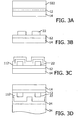
- Figures 3A to 3D illustrate manufacturing of a transparent layer stack or transparent body, which can for example be used for a touch panel display.
- the layer stack 12 is provided over the transparent substrate 14.
- the transparent substrate can be a flexible substrate or a rigid substrate, an organic substrate or an inorganic substrate, can be a glass or a foil, and can have other characteristics like being linearly or circular polarizing, a lambda quarter retarder or non-polarizing.
- the transparent substrate can have a high degree of transparency in the visible range of 380 nm to 780 nm.
- the transparent substrate 14 can include glass (flexible or rigid), plastic (flexible or rigid), which can further be already covered with thin film layers or hard coat, a linear or circular polarizer material, or lambda quarter retarder.
- glass substrates deposition processes and manufacturing methods on the glass substrate can be provided at higher temperatures as compared to plastic substrates. For example temperatures of 150°C or above or even temperatures of 200°C or above, such as 300 °C, can be utilized for manufacturing of transparent bodies for the touch panel display on glass substrates.
- the layer stack 12 is typically an index matching layer stack having at least a first and a second dielectric film, wherein the first refractive index is provided by the first electric film and the second refractive index is provided by the second dielectric film, and wherein the second refractive index is lower from the first refractive index.
- a first dielectric film, a second dielectric film and a plurality of further dielectric films can be deposited such that a continuous or quasi-continuous (e.g. step-like with small steps) change in refractive index can be generated in the transparent layer stack 12.
- the dielectric films can be manufactured by chemical vapor deposition or physical vapor deposition, for example sputtering or evaporation.
- Typical examples can be insulating materials with high and low refractive indexes, for example SiOx, MgF, TiOx, NbOx, SiNx, SiOxNy, AlOx, AlOxNy, TaOx, and combinations thereof.
- the transparent conductive layer stack has increased conductivity by providing an increased layer thickness or a decreased specific resistance of the layer material.
- TCO layer thicknesses of 40 nm and above, e.g. 50 nm to 150 nm can be utilized.
- the transparent conductive oxide layer can also be provided as a transparent conductive oxide layer stack having one or more transparent conductive oxide films.
- the transparent conductive oxide film or transparent conductive film stack can be heated during or after deposition, for example by thermal heating or by RTP flashlights.
- the transparent conductive oxide can be heated to temperatures of 80°C or above.
- the manufacturing of the transparent conductive oxide films can be provided by chemical vapor deposition or physical vapor deposition, e.g. sputtering or evaporation. In order to provide a high yield of manufacturing, for example DC sputtering of a transparent conductive oxide layer from a rotatable target can be provided.
- Typical examples of the transparent conductive oxide or the transparent conductive oxide layer stack can be ITO, doped ITO, , impurity-doped ZnO, In 2 O 3 , SnO 2 and CdO, ITO (In2O3:Sn), AZO (ZnO:Al), IZO (ZnO: In), GZO (ZnO:Ga), multi-component oxides including or consisting of combinations of ZnO, In 2 O 3 and SnO 2 , a layer stack from at least an ITO layer and a metal layer, e.g. an ITO/metal/ITO-stack or a metal/ITO/metal-stack.
- the transparent conductive oxide layer 322 (see figure 3A ) is structured to provide a structured transparent conductive oxide layer 22.
- the structured TCO layer can be provided by depositing a TCO layer and patterning the TCO layer in order to provide a structured TCO layer. Further, a mask and/or a photoresist can be provided to deposit the structured TCO layer.
- Figure 3C illustrates deposition of a second transparent layer stack 112 over the TCO structured TCO layer 22.
- the layer stack 112 is typically an index matching layer stack having at least a first dielectric film of the second transparent stack and a second dielectric film of the second transparent stack, wherein the first refractive index is provided by the first electric film and the second refractive index is provided by the second dielectric film, and wherein the second refractive index is lower from the first refractive index.
- a first dielectric film, a second dielectric film and a plurality of further dielectric films can be deposited in the second transparent layer stack such that a continuous or quasi-continuous (e.g. step-like with small steps) change in refractive index can be generated in the second transparent layer stack 112.
- the dielectric films can be manufactured by chemical vapor deposition or physical vapor deposition, for example sputtering or evaporation. Typical examples can be insulating materials with high and low refractive indexes, for example SiOx, TiOx, NbOx, SiNx, SiOxNy, AlOx, TaOx, and combinations thereof.
- Figure 3D illustrates a transparent adhesive 24, such as an optically clear adhesive in order to bond the transparent body to the display 34.
- the transparent adhesive can be an optical clear adhesive laminate or liquid optical clear adhesive with a refractive index close to a second substrate or polarizer, i.e. the substrate or polarizer of the display 34.
- the refractive index can be close to the refractive index of glass (1.48) or of PMMA (1.6), for example, in the range between 1.48 and 1.6.
- the transparent adhesive can have a visual transmittance of 95% or above, 97% or above , or even 99% or above.
- a structure TCO layer e.g. an ITO layer, two index matching layers and a transparent adhesive configured for bonding to a display, a color filter, an electro-optical device, or the like, is provided such that the two index matching layer on both sides of the TCO layer provide essentially invisibility of the structures of the TCO.
- the layer stack for example a touch panel layer stack or transparent body, can be bonded to or integrated in a display device with improved visual and electrical characteristics.
- layer stack or transparent body it is referred to layer stack or transparent body. It will be appreciated that these terms are used synonymously here, e.g. a transparent body is also provided by a stack of layers or films, i.e. a transparent body is also a layer stack.
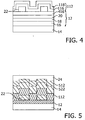
- Figure 4 illustrates yet further embodiments, which can be combined with other embodiments described herein.
- the substrate of the transparent body which can for example be used in a touch panel, is provided.
- the substrate can be, for example, the cover lens after the transparent touch body is bonded to an electro-optical device, such as a display or the like.
- the embodiments described with respect to figure 4 include four dielectric layers 16, 18, 20 and 416, which form a transparent layer stack.
- the structured transparent conductive film 22 is provided on top of the transparent layer stack.
- the transparent conductive oxide film can be TCO layer, which is deposited by DC sputtering from a rotatable target. However, other position techniques might be applied as well. Sputtering from a rotatable target is, for example useful for manufacturing of large area devices.
- large area substrates or respective carriers wherein the carriers have a plurality of substrates, may have a size of at least 0.174 m 2 .
- the size can be about 0.67m 2 (0.73x0.92m - Gen 4.5) to about 8 m 2 , more typically about 2 m 2 to about 9 m 2 or even up to 12 m 2 .
- the substrates or carriers, for which the structures, apparatuses, such as cathode assemblies, and methods according to embodiments described herein are provided are large area substrates as described herein.
- a large area substrate or carrier can be GEN 4.5, which corresponds to about 0.67 m2 substrates (0.73x0.92m), GEN 5, which corresponds to about 1.4 m 2 substrates (1.1 m x 1.3 m), GEN 7.5, which corresponds to about 4.29 m 2 substrates (1.95 m x 2.2 m), GEN 8.5, which corresponds to about 5.7m 2 substrates (2.2 m x 2.5 m), or even GEN 10, which corresponds to about 8.7 m 2 substrates (2.85 m x 3.05 m). Even larger generations such as GEN 11 and GEN 12 and corresponding substrate areas can similarly be implemented.
- the index matching layer stack 12 as shown in figure 4 , together with the second transparent layer stack having dielectric layers 116 and 118 results in improved optical characteristics.
- the structures of the TCO layer are essentially invisible to the user of such a device due to the two transparent layer stacks. According to embodiments described herein, this can be provided for the transparent conductive films having a sheet resistance of 100 Ohm/square or below, for example transparent conductive oxide layers of 20 nm or above, or even 100 nm or above. According to different embodiments, which can be combined with other embodiments described herein, two or more dielectric layers can be provided in the transparent layer stack 12
- the two or more layers can be a plurality of dielectric layers or films, for example, such that a gradient in the refractive index in the layer stack is provided.
- a first dielectric film can be provided with a first refractive index and the refractive index can be changed during further deposition of the transparent layer stack. The change can be continuous or step-like.
- further dielectric films (16-20; 416) can be provided, wherein a refractive index can be obtained in the transparent layer stack.
- the combination of the transparent layer stack 12 and the transparent conductive film can be repeated twice, three times or even four times.
- Figure 5 shows a transparent layer stack 12 deposited over the substrate 14.
- the structured transparent conductive film 22 is provided on the transparent layer stack 12.
- a second transparent layer stack 112 and a further transparent conductive film 522 are deposited.
- different refractive indices are provided for adjacent films.
- the second transparent conductive film 522 is provided over the second transparent layer stack 112.
- the cross-section illustrated in figure 5 does not show a structuring of the second transparent conductive film 522. However, the structuring can be applied in the direction different as compared to the paper plane.
- the transparent adhesive 24 is provided on the further transparent layer stack 512 and is configured for bonding the transparent body to the electro-optical device, such a display or the like.
- the first transparent layer stack, the transparent conductive film, and the second transparent layer stack 112 are deposited in a manner such that the a* and b* value for the manufactured transparent body is below 1.5 or, in particular 1, or more specifically, 0.7, or, even more specifically, 0.2.
- the a* and b* value for the structure formed solely by the first transparent layer stack, the transparent conductive film, and the transparent adhesive, and placed above a substantially transparent substrate may adopt these values.
- FIG. 6 shows a deposition apparatus 600.
- one vacuum chamber 602 for deposition of layers therein is shown.
- further chambers can be provided adjacent to the chamber 602.
- the vacuum chamber 602 can be separated from adjacent chambers by a valve having a valve housing 604 and the valve unit 605.
- the valve unit 605 can be closed.
- the atmosphere in the vacuum chambers can be individually controlled by generating a technical vacuum, for example with vacuum pumps connected to the chamber 602, and/or by inserting process gases in the deposition region in the chamber.
- process gases can include inert gases such as argon and/or reactive gases such as oxygen, nitrogen, hydrogen and ammonia (NH3), Ozone (03), or activated gases or the like.
- inert gases such as argon and/or reactive gases such as oxygen, nitrogen, hydrogen and ammonia (NH3), Ozone (03), or activated gases or the like.
- reactive gases such as oxygen, nitrogen, hydrogen and ammonia (NH3), Ozone (03), or activated gases or the like.
- the groups of deposition sources 622 and 624 are illustrated in FIG. 6 .
- the groups of deposition sources can typically be provided in different chambers in the event different deposition processes are provided by the groups of deposition sources.
- the deposition sources can for example be rotatable cathodes having targets of the material to be deposited on the substrate.
- the cathodes can be rotatable cathodes with a magnetron therein. Thereby, magnetron sputtering can be conducted for depositing of the layers.
- Cathodes 622 are connected to an AC power supply 623 such that the cathodes can be biased in an alternating manner.
- magnet sputtering refers to sputtering performed using a magnet assembly, that is, a unit capable of a generating a magnetic field.
- a magnet assembly consists of a permanent magnet.
- This permanent magnet is typically arranged within a rotatable target or coupled to a planar target in a manner such that the free electrons are trapped within the generated magnetic field generated below the rotatable target surface.
- Such a magnet assembly may also be arranged coupled to a planar cathode.
- magnetron sputtering can be realized by a double magnetron cathode, i.e. cathodes 622, such as, but not limited to, a TwinMagTM cathode assembly.
- cathodes 622 such as, but not limited to, a TwinMagTM cathode assembly.
- target assemblies including double cathodes can be applied.
- the cathodes in a deposition chamber may be interchangeable. Accordingly, the targets are changed after the silicon has been consumed.
- that dielectric layers can be deposited by sputtering, for example magnetron sputtering, of rotatable cathodes having an AC power supply.
- MF sputtering can be applied for depositing the dielectric layers.
- sputtering from a silicon target e.g. a sprayed silicon target
- MF sputtering that is middle frequency sputtering.
- middle frequency is a frequency in the range 5 kHz to 100 kHz, for example, 10 kHz to 50 kHz.
- Sputtering from a target for a transparent conductive oxide film is typically conducted as DC sputtering.
- the cathodes 624 are connected to the DC power supply 626 together with anodes 625 collecting electrons during sputtering.
- the transparent conductive oxide layers for example the ITO layers, can be sputtered by DC sputtering, i.e. an assembly having cathodes 624.
- the cathodes 622 and 624 are illustrated to be provided in one vacuum chamber 602.
- the cathodes for depositing different layers are provided in different vacuum chamber, for example the chamber 602 and the vacuum chambers adjacent to the vacuum chamber 602, as illustrated by the lower cathodes 622 in FIG. 6 .
- the dielectric layers, as described herein, which can be oxide-layers, nitrite-layers, or oxinitride-layers can be deposited by a reactive deposition process where the target material reacts with oxygen and/or nitrogen after the material has been released from the target.
- an atmosphere with an appropriate processing gas and/or the appropriate degree of technical vacuum can be provided in each deposition area.
- two or more groups of cathodes 622 can be provided in the deposition apparatus 600.
- deposition is performed by sputtering of one or more rotatable targets. More specifically, according to embodiments herein, at least one of the films referred to above is deposited by sputtering of a rotatable target, so that formation of a stable transparent body and with a high quality is facilitated.
- a film may be deposited having a higher uniformity, and with a low density of defects and contamination particles. Thereby, it is facilitated manufacturing of a high-quality transparent body that not only yields a proper transmission of light but also yields a stable performance over time.
- a manufacturing process including sputtering of one or more rotatable targets may further facilitate a higher manufacturing rate and the production of a lower number of contaminant particles as compared to other deposition methods.
- Figure 7 shows a flowchart 700 illustrating a process for manufacturing a transparent body as described herein.
- the first transparent layer stack e.g. layers stack 12
- the layer stack includes at least two dielectric films, wherein the refractive indices of the dielectric films are different from each other and films with a higher refractive index and films with the lower refractive index can be deposited in an alternating manner.
- the structured transparent conductive film for example structured ITO layer, is deposited over the transparent layer stack 12.
- the structured transparent conductive film can be also a stack of conductive films.
- a TCO/metal/TCO-stack can be provided in step 704.
- structuring procedures can be selected from the group consisting of: (1) laser scribing, (2) photo lithography, (3) printing adsorption barrier pattern (e.g. oil) followed by TCO deposition, (4) a lift-off process (formation of photo-resist pattern on substrate followed by TCO deposition and lift-off with photo-resist solvent), (5) film deposition using a shadow mask, or combinations thereof.
- adsorption barrier pattern e.g. oil
- lift-off process formation of photo-resist pattern on substrate followed by TCO deposition and lift-off with photo-resist solvent
- film deposition using a shadow mask or combinations thereof.
- one or some of the chambers may be configured for performing sputtering without a magnetron assembly.
- One or some chambers, for example additional chamber, may be configured for performing deposition by other methods, such as, but not limited to, chemical vapor deposition or pulsed laser deposition.
- the deposition apparatuses as described herein can further include a measurement system 638 configured for measuring during deposition optical properties of at least one of the films forming part of at least one of the first layer stack or the transparent conductive film.
- the dielectric films can be typically reactively sputtered.
- the first deposition assembly (622) can be configured for depositing the dielectric films by reactive sputtering.
- Si-containing layers or A1 containing layers can be sputtered reactively, and/or Nb-containing layers, Ti-containing layers or ITO-containing layers can be sputtered from a ceramic target.
- exemplary process 700 may further include a heating treatment of the substrate for degassing of the substrate prior to deposition.
- the substrate may be heated at a temperature between 60 and 360 °C depending on the substrate speed.
- exemplary process 700 may include performing a DC and/or medium frequency (MF) pre-treatment of the substrate with a power between 1 and 3 kW.
- exemplary process 700 may include performing a pre-treatment of the substrate at an argon and/or oxygen atmosphere such as, for example, an oxygen rich pre-treatment.
- medium frequency is a frequency in the range of 5 kHz to 100 kHz, for example, 30 kHz to 50 kHz.
- the sputter coating sources in the exemplary deposition apparatuses or in an apparatus according to embodiments herein may be a DC-cathode with planar or rotatable targets (such as, but not limited to, ceramic ITO), and planar or rotatable targets (such as a doped silicon target, in particular sprayed Si targets for depositing SiO 2 , or Si3N4, SiOxNy) or targets including a material to deposit one of the other dielectric layers disclosed herein.
- planar or rotatable targets such as, but not limited to, ceramic ITO
- planar or rotatable targets such as a doped silicon target, in particular sprayed Si targets for depositing SiO 2 , or Si3N4, SiOxNy
- the transparent conductive film has a sheet resistance of 100 Ohm/square or below.
- This can be provided by providing a comparably thick transparent conductive layer and/or utilizing a TCO material with a low specific resistivity. This results in a more complex index-matching situation for reaching the required high optical performance such as pattern invisibility, color neutrality and high transmittance levels.
- a second transparent layer stack e.g., layers stack 12
- the layer stack includes at least two dielectric films, wherein the refractive indices of the dielectric films are different from each other and films with a higher refractive index and films with the lower refractive index can be deposited in an alternating manner.
- a transparent adhesive for example an optically clear adhesive, is provided in order to bond the transparent body to an electro-optical device, such as a display, a display of a mobile phone, a display of the touch panel TV, a display of the touch panel computer, or the like.
- the transparent body i.e. the thin film stacks
- the transparent body are produced involving magnetron sputtering from rotary targets.
- invisible ITO solutions have extremely high demands on the optical uniformity of optical properties (color values in transmission and reflection), which corresponds technically to the deposition of very uniform films with respect to film thickness and optical dispersion properties. Accordingly, longer targets than the targeted sputtering height can be utilized.
- planar targets have-deposition zones, which are responsible for enhanced particle generation, and hence need to be much longer than rotary targets to provide for particle-free and uniform films.
Landscapes
- Engineering & Computer Science (AREA)
- Chemical & Material Sciences (AREA)
- Physics & Mathematics (AREA)
- Plasma & Fusion (AREA)
- Analytical Chemistry (AREA)
- General Engineering & Computer Science (AREA)
- Theoretical Computer Science (AREA)
- General Physics & Mathematics (AREA)
- Chemical Kinetics & Catalysis (AREA)
- Materials Engineering (AREA)
- Mechanical Engineering (AREA)
- Metallurgy (AREA)
- Organic Chemistry (AREA)
- Human Computer Interaction (AREA)
- Optics & Photonics (AREA)
- Inorganic Chemistry (AREA)
- Laminated Bodies (AREA)
- Physical Vapour Deposition (AREA)
- Position Input By Displaying (AREA)
Claims (16)
- Procédé pour la fabrication d'un corps transparent (10) destiné à être utilisé dans un écran d'affichage tactile, le procédé comprenant :le dépôt d'une première pile de couches transparentes (12) sur un substrat transparent (14), ladite première pile de couches transparentes (12) comprenant au moins un premier film diélectrique (16) avec un premier indice de réfraction, et un deuxième film diélectrique (18) avec un deuxième indice de réfraction différent du premier indice de réfraction ;la mise à disposition d'un film conducteur transparent structuré (22) de telle façon que la première pile de couches transparentes (12) et le film conducteur transparent (22) sont disposés sur le substrat transparent (14) dans cet ordre, le film conducteur transparent structuré correspondant à une résistance de feuille de 100 Ohms/carré ou moins ; etle dépôt d'une deuxième pile de couches transparentes sur le film conducteur transparent, la deuxième pile de couches transparentes étant sélectionnée parmi le groupe comprenant :une pile de couches, la pile de couches comprenant un troisième film diélectrique avec un gradient d'indice de réfraction d'un troisième indice de réfraction à un quatrième indice de réfraction différent du troisième indice de réfraction, etune pile de couches, la pile de couches comprenantau moins un troisième film diélectrique avec un troisième indice de réfraction, etun quatrième film diélectrique ou un adhésif transparent, respectivement avec un quatrième indice de réfraction différent du troisième indice de réfraction,dans lequel le film conducteur transparent structuré et la deuxième pile de couches transparentes sont disposés dans cet ordre.
- Procédé selon la revendication 1, dans lequel au moins l'un parmi le premier film diélectrique (16), le deuxième film diélectrique (18) ou le film conducteur transparent (22) est déposé par pulvérisation d'une cible, en particulier d'une cible rotative.
- Procédé selon l'une quelconque des revendications 1 à 2, dans lequel la mise à disposition du film conducteur transparent structuré comprend la texturation d'un film conducteur transparent déposé non structuré.
- Procédé selon l'une quelconque des revendications 1 à 3, dans lequel le premier film diélectrique présente un indice de réfraction d'au moins 1,8 et le deuxième film diélectrique présente un indice de réfraction de 1,5 ou moins ; et/ou dans lequel le troisième film diélectrique présente un indice de réfraction d'au moins 1,8 et le quatrième film diélectrique présente un indice de réfraction de 1,5 ou moins.
- Procédé selon l'une quelconque des revendications 1 à 4, dans lequel les films diélectriques sont pulvérisés par pulvérisation MF, typiquement à partir d'une cible rotative, et les films conducteurs transparents sont pulvérisés par pulvérisation DC, typiquement à partir d'une cible rotative.
- Procédé selon l'une quelconque des revendications 1 à 5, dans lequel le film conducteur transparent structuré est disposé directement entre un film diélectrique à indice de réfraction faible et un film diélectrique à indice de réfraction élevé.
- Corps transparent adapté pour être utilisé dans un écran d'affichage tactile, comprenant :un substrat transparent ;une première pile de couches transparentes déposé sur le substrat transparent, ladite première pile de couches transparentes (12) comprenant au moins un premier film diélectrique (16) avec un premier indice de réfraction, et un deuxième film diélectrique (18) avec un deuxième indice de réfraction différent du premier indice de réfraction ; un film conducteur transparent déposé sur la première pile de couches transparentes, le film conducteur transparent structuré correspondant à une résistance de feuille de 100 Ohms/carré ou moins ; etune deuxième pile de couches transparentes sur le film conducteur transparent, ladite deuxième pile de couches transparentes étant sélectionnée parmi le groupe comprenant :une pile de couches, la pile de couches comprenant un troisième film diélectrique avec un gradient d'indice de réfraction d'un troisième indice de réfraction à un quatrième indice de réfraction différent du troisième indice de réfraction, etune pile de couches, la pile de couches comprenantau moins un troisième film diélectrique avec un troisième indice de réfraction, etun quatrième film diélectrique ou un adhésif transparent, respectivement avec un quatrième indice de réfraction différent du troisième indice de réfraction.
- Corps transparent selon la revendication 7, dans lequel le premier film diélectrique présente un indice de réfraction d'au moins 1,8 et le deuxième film diélectrique présente un indice de réfraction de 1,5 ou moins ; et/ou dans lequel le troisième film diélectrique présente un indice de réfraction d'au moins 1,8 et le quatrième film diélectrique présente un indice de réfraction de 1,5 ou moins.
- Corps transparent selon l'une quelconque des revendications 7 à 8, dans lequel le substrat transparent est sélectionné parmi le groupe comprenant : un substrat rigide, un substrat souple, un substrat organique, un substrat inorganique, un verre, une feuille de plastique, un substrat à base de matériau polarisant, et un substrat à base de retardateur lambda/4.
- Corps transparent selon l'une quelconque des revendications 7 à 9, dans lequel la première pile de couches transparentes et la deuxième pile de couches transparentes sont des piles de couches d'adaptation d'indice et/ou sont sélectionnées parmi le groupe comprenant : SiOx, SiNx, SiOxNy, AlOx, AlOxNy, TiOx, TaOx, MgFx et NbOx.
- Corps transparent selon l'une quelconque des revendications 7 à 10, dans lequel le film conducteur transparent présente une épaisseur de 20 nm ou plus, en particulier de 50 nm à 150 nm.
- Corps transparent selon l'une quelconque des revendications 7 à 11, dans lequel le film conducteur transparent contient de l'oxyde d'indium-étain.
- Corps transparent selon l'une quelconque des revendications 7 à 12, dans lequel le film conducteur transparent est disposé sur un film diélectrique avec un indice de réfraction de 1,5 ou moins et un film diélectrique avec un indice de réfraction de 1,8 ou plus est disposé sur le film conducteur transparent.
- Corps transparent selon l'une quelconque des revendications 7 à 13, dans lequel un adhésif transparent est disposé pour relier la pile de couches à l'écran d'affichage tactile.
- Appareil de dépôt (600) pour la fabrication d'un corps transparent (10) destiné à être utilisé dans un écran d'affichage tactile, ledit appareil comprenant :un premier ensemble de dépôt (622) configuré pour déposer une première pile de couches transparentes (12) sur un substrat (14), ladite première pile de couches transparentes (12) comprenant au moins un premier film diélectrique (16) avec un premier indice de réfraction, et un deuxième film diélectrique (18) avec un deuxième indice de réfraction différent du premier indice de réfraction ;un deuxième ensemble de dépôt (624) configuré pour déposer un film conducteur transparent (22) ; etun troisième ensemble de dépôt (622) configuré pour déposer une deuxième pile de couches transparentes (112) sur le film conducteur transparent (14), ladite deuxième pile de couches transparentes (12) comprenant au moins un troisième film diélectrique (16) avec un troisième indice de réfraction ;dans lequel ledit premier ensemble de dépôt (622), ledit deuxième ensemble de dépôt (624) et le troisième ensemble de dépôt sont arrangés de telle façon que la première pile de couches transparentes (12), le film conducteur transparent (22) et la deuxième pile de couches transparentes sont disposés sur le substrat (14) dans cet ordre, et dans lequel au moins l'un parmi le premier ensemble de dépôt (622) ou le deuxième ensemble de dépôt ou le troisième ensemble de dépôt comprend un système de pulvérisation fonctionnellement accouplé à une cible, ledit système de pulvérisation étant configuré pour déposer au moins l'un parmi le premier film diélectrique (16), le deuxième film diélectrique (18), le troisième film diélectrique ou le film conducteur transparent (22) par pulvérisation de la cible.
- Appareil selon la revendication 15, dans lequel le premier ensemble de dépôt (6222), le deuxième ensemble de dépôt (624) ou le troisième ensemble de dépôt sont configurés pur déposer la première pile transparente (12), la deuxième pile transparente (112) et le film conducteur transparent (22) par pulvérisation au magnétron, typiquement par pulvérisation au magnétron à partir d'une cible rotative.
Applications Claiming Priority (1)
| Application Number | Priority Date | Filing Date | Title |
|---|---|---|---|
| PCT/EP2012/055869 WO2013143615A1 (fr) | 2012-03-30 | 2012-03-30 | Corps transparent destiné à être utilisé dans un panneau tactile et son procédé de fabrication et appareil |
Publications (2)
| Publication Number | Publication Date |
|---|---|
| EP2831708A1 EP2831708A1 (fr) | 2015-02-04 |
| EP2831708B1 true EP2831708B1 (fr) | 2017-10-18 |
Family
ID=45922692
Family Applications (1)
| Application Number | Title | Priority Date | Filing Date |
|---|---|---|---|
| EP12711408.0A Active EP2831708B1 (fr) | 2012-03-30 | 2012-03-30 | Corps transparent destiné à être utilisé dans un panneau tactile et son procédé de fabrication et appareil |
Country Status (7)
| Country | Link |
|---|---|
| US (1) | US10281616B2 (fr) |
| EP (1) | EP2831708B1 (fr) |
| JP (1) | JP6307062B2 (fr) |
| KR (1) | KR101890781B1 (fr) |
| CN (1) | CN104246667B (fr) |
| TW (1) | TWI606373B (fr) |
| WO (1) | WO2013143615A1 (fr) |
Families Citing this family (24)
| Publication number | Priority date | Publication date | Assignee | Title |
|---|---|---|---|---|
| EP2753960B1 (fr) * | 2011-09-07 | 2016-12-07 | Applied Materials, Inc. | Procédé et système de fabrication d'un corps transparent pour utilisation dans un écran tactile |
| WO2014007157A1 (fr) * | 2012-07-02 | 2014-01-09 | シャープ株式会社 | Panneau tactile et appareil d'affichage pourvu d'un panneau tactile |
| CN103425325B (zh) * | 2013-03-30 | 2016-12-28 | 南昌欧菲光显示技术有限公司 | 偏光片模块及其制备方法和触摸显示屏 |
| US9110230B2 (en) | 2013-05-07 | 2015-08-18 | Corning Incorporated | Scratch-resistant articles with retained optical properties |
| US9366784B2 (en) | 2013-05-07 | 2016-06-14 | Corning Incorporated | Low-color scratch-resistant articles with a multilayer optical film |
| EP2863291A1 (fr) * | 2013-10-18 | 2015-04-22 | Applied Materials, Inc. | Corps transparent pour procédé de fabrication de panneau tactile et système de fabrication d'un corps transparent pour un tel panneau |
| US11267973B2 (en) * | 2014-05-12 | 2022-03-08 | Corning Incorporated | Durable anti-reflective articles |
| US9790593B2 (en) | 2014-08-01 | 2017-10-17 | Corning Incorporated | Scratch-resistant materials and articles including the same |
| CN104777930B (zh) * | 2015-02-09 | 2017-12-08 | 合肥鑫晟光电科技有限公司 | Ogs触摸屏及其制造方法、ogs触摸装置 |
| CN107250965A (zh) * | 2015-02-12 | 2017-10-13 | 应用材料公司 | 适于用于光电装置中的层堆叠、光电装置、以及适于用于光电装置中的层堆叠的制造方法 |
| CN104571721B (zh) * | 2015-02-17 | 2018-11-23 | 合肥鑫晟光电科技有限公司 | 一种透明导电氧化物图案消隐结构、触控面板及显示装置 |
| JP6639098B2 (ja) * | 2015-03-20 | 2020-02-05 | 富士フイルム株式会社 | タッチパネル部材、タッチパネル及びタッチパネル表示装置 |
| EP3296277B1 (fr) * | 2015-05-11 | 2021-01-13 | AGC Inc. | Vitrage thermo-isolant pour véhicule et son procédé de fabrication |
| WO2016181739A1 (fr) * | 2015-05-11 | 2016-11-17 | 旭硝子株式会社 | Unité de verre isolant contre la chaleur pour véhicule |
| JP6688033B2 (ja) * | 2015-05-27 | 2020-04-28 | 日東電工株式会社 | 透明導電性フィルム |
| CN106325577B (zh) * | 2015-06-28 | 2023-07-25 | 宸鸿科技(厦门)有限公司 | 触控装置及其制造方法 |
| WO2017048700A1 (fr) | 2015-09-14 | 2017-03-23 | Corning Incorporated | Articles anti-réfléchissants de transmission de lumière élevée et résistants aux rayures |
| KR102415044B1 (ko) * | 2015-12-11 | 2022-07-01 | 삼성디스플레이 주식회사 | 터치 스크린 패널, 이의 제조 방법 및 터치 스크린 패널을 포함하는 터치 표시 장치 |
| MX2019000869A (es) | 2018-01-30 | 2019-12-19 | Viavi Solutions Inc | Dispositivo óptico que tiene partes ópticas y mecánicas. |
| US11187836B2 (en) | 2018-03-06 | 2021-11-30 | Applied Materials, Inc. | Method of building a 3D functional optical material layer stacking structure |
| KR102591065B1 (ko) | 2018-08-17 | 2023-10-19 | 코닝 인코포레이티드 | 얇고, 내구성 있는 반사-방지 구조를 갖는 무기산화물 물품 |
| CN111399701B (zh) * | 2020-05-09 | 2024-04-02 | 上海天马微电子有限公司 | 触控模组、触控显示面板和触控显示装置 |
| CN113672107B (zh) * | 2020-05-14 | 2024-06-21 | 瀚宇彩晶股份有限公司 | 触控显示设备 |
| CN115505884A (zh) * | 2021-06-23 | 2022-12-23 | 江西华派光电科技有限公司 | 一种高透光蓝宝石面板及其制作方法 |
Family Cites Families (27)
| Publication number | Priority date | Publication date | Assignee | Title |
|---|---|---|---|---|
| CN1188869C (zh) * | 1999-08-31 | 2005-02-09 | 帝人株式会社 | 透明导电叠层板和使用这种板的触摸屏 |
| CN100376907C (zh) | 2002-12-20 | 2008-03-26 | 帝人株式会社 | 透明导电性层压体、触摸屏和带有触摸屏的液晶显示装置 |
| JP2006023904A (ja) | 2004-07-07 | 2006-01-26 | Sony Corp | 薄型静電容量式タッチパネル及び液晶表示装置 |
| JP4532316B2 (ja) * | 2005-03-22 | 2010-08-25 | 日本板硝子株式会社 | タッチパネル |
| KR101192391B1 (ko) | 2005-05-26 | 2012-10-17 | 군제 가부시키가이샤 | 투명 평면체 및 투명 터치스위치 |
| JP4883383B2 (ja) * | 2005-06-02 | 2012-02-22 | 旭硝子株式会社 | 中空状SiO2を含有する分散液、塗料組成物及び反射防止塗膜付き基材 |
| JP4883772B2 (ja) * | 2006-07-13 | 2012-02-22 | キヤノン株式会社 | 画像処理装置及び方法 |
| JP4314623B2 (ja) * | 2006-12-07 | 2009-08-19 | 日東電工株式会社 | 透明導電性積層体及びタッチパネル |
| CN101200349A (zh) * | 2006-12-14 | 2008-06-18 | 财团法人工业技术研究院 | 硬质抗反射透明沸石层及其制造方法和产生沸石层的溶液 |
| CN101359267A (zh) * | 2007-07-30 | 2009-02-04 | 比亚迪股份有限公司 | 一种电容式触摸屏及其制作方法 |
| CN101498972B (zh) * | 2008-02-01 | 2012-07-18 | 台达电子工业股份有限公司 | 触控面板 |
| TW200936706A (en) * | 2008-02-19 | 2009-09-01 | Univ Nat Central | Coating composition for low-refractive index anti-reflection film |
| CN101581800A (zh) | 2008-05-15 | 2009-11-18 | 甘国工 | 复合导电膜及使用该膜的触摸屏 |
| JP4966924B2 (ja) * | 2008-07-16 | 2012-07-04 | 日東電工株式会社 | 透明導電性フィルム、透明導電性積層体及びタッチパネル、並びに透明導電性フィルムの製造方法 |
| JP5160325B2 (ja) * | 2008-07-16 | 2013-03-13 | 日東電工株式会社 | 透明導電性フィルム及びタッチパネル |
| JP5788129B2 (ja) * | 2008-07-18 | 2015-09-30 | 日東電工株式会社 | 透明導電性フィルム及びタッチパネル |
| JP2010086684A (ja) * | 2008-09-30 | 2010-04-15 | Kuramoto Seisakusho Co Ltd | 透明導電配線膜付き光学薄膜 |
| CN101713834B (zh) * | 2008-10-07 | 2011-12-14 | 甘国工 | 高透光导电膜系 |
| CN101504496A (zh) * | 2009-03-04 | 2009-08-12 | 信利半导体有限公司 | 一种触摸屏和平板显示模块一体化组合模块及其制作方法 |
| JP4958020B2 (ja) * | 2009-03-31 | 2012-06-20 | 大日本印刷株式会社 | タッチパネルセンサ、タッチパネルセンサを作製するための積層体、および、タッチパネルセンサの製造方法 |
| CN102043495B (zh) * | 2009-10-21 | 2012-11-21 | 比亚迪股份有限公司 | 一种导电元件及其制备方法、一种触摸屏面板 |
| CN102194539A (zh) * | 2010-03-11 | 2011-09-21 | 联享光电股份有限公司 | 透明导电叠层体及其制造方法 |
| EP2402481A1 (fr) * | 2010-06-29 | 2012-01-04 | Applied Materials, Inc. | Procédé et système pour fabriquer un corps transparent pour une utilisation dans un panneau tactile |
| JP2012058956A (ja) * | 2010-09-08 | 2012-03-22 | Sony Corp | 電極フィルム及び座標検出装置 |
| JP5739742B2 (ja) * | 2010-11-04 | 2015-06-24 | 日東電工株式会社 | 透明導電性フィルムおよびタッチパネル |
| EP2753960B1 (fr) * | 2011-09-07 | 2016-12-07 | Applied Materials, Inc. | Procédé et système de fabrication d'un corps transparent pour utilisation dans un écran tactile |
| EP2863291A1 (fr) * | 2013-10-18 | 2015-04-22 | Applied Materials, Inc. | Corps transparent pour procédé de fabrication de panneau tactile et système de fabrication d'un corps transparent pour un tel panneau |
-
2012
- 2012-03-30 WO PCT/EP2012/055869 patent/WO2013143615A1/fr active Application Filing
- 2012-03-30 JP JP2015502112A patent/JP6307062B2/ja active Active
- 2012-03-30 KR KR1020147030596A patent/KR101890781B1/ko active IP Right Grant
- 2012-03-30 EP EP12711408.0A patent/EP2831708B1/fr active Active
- 2012-03-30 CN CN201280071777.6A patent/CN104246667B/zh active Active
- 2012-03-30 US US14/384,820 patent/US10281616B2/en active Active
-
2013
- 2013-03-29 TW TW102111490A patent/TWI606373B/zh active
Non-Patent Citations (1)
| Title |
|---|
| None * |
Also Published As
| Publication number | Publication date |
|---|---|
| CN104246667B (zh) | 2018-04-10 |
| JP2015518518A (ja) | 2015-07-02 |
| TW201403415A (zh) | 2014-01-16 |
| EP2831708A1 (fr) | 2015-02-04 |
| CN104246667A (zh) | 2014-12-24 |
| US20150062710A1 (en) | 2015-03-05 |
| TWI606373B (zh) | 2017-11-21 |
| KR20140141706A (ko) | 2014-12-10 |
| US10281616B2 (en) | 2019-05-07 |
| WO2013143615A1 (fr) | 2013-10-03 |
| JP6307062B2 (ja) | 2018-04-04 |
| KR101890781B1 (ko) | 2018-08-22 |
Similar Documents
| Publication | Publication Date | Title |
|---|---|---|
| EP2831708B1 (fr) | Corps transparent destiné à être utilisé dans un panneau tactile et son procédé de fabrication et appareil | |
| EP2831707B1 (fr) | Corps transparent destiné à être utilisé dans un procédé de fabrication de panneau d'écran tactile et système | |
| US10175829B2 (en) | Transparent body with single substrate and anti-reflection and/or anti-fingerprint coating at an opposite side of the substrate from a structured transparent conductive film, and method of manufacturing thereof | |
| US9920421B2 (en) | Transparent body for a touch panel manufacturing method and system for manufacturing a transparent body for a touch screen panel | |
| JP2015518596A5 (fr) | ||
| US20110318553A1 (en) | Method and system for manufacturing a transparent body for use in a touch panel | |
| CN105144045A (zh) | 导电结构及其制造方法 | |
| CN104516586A (zh) | 触控面板及其制造方法 | |
| WO2016128054A1 (fr) | Empilement de couches conçu pour être utilisé dans un dispositif électro-optique, son procédé de fabrication et dispositif électro-optique | |
| KR101955005B1 (ko) | 터치 스크린 패널에서 사용하기 위한 층 시스템, 터치 스크린 패널에서 사용하기 위한 층 시스템을 제조하기 위한 방법, 및 터치 스크린 패널 | |
| Switzer III | Characterization of physical vapor deposited and patterned thin films for roll-to-roll flexible passive and active electronic devices |
Legal Events
| Date | Code | Title | Description |
|---|---|---|---|
| PUAI | Public reference made under article 153(3) epc to a published international application that has entered the european phase |
Free format text: ORIGINAL CODE: 0009012 |
|
| 17P | Request for examination filed |
Effective date: 20141014 |
|
| AK | Designated contracting states |
Kind code of ref document: A1 Designated state(s): AL AT BE BG CH CY CZ DE DK EE ES FI FR GB GR HR HU IE IS IT LI LT LU LV MC MK MT NL NO PL PT RO RS SE SI SK SM TR |
|
| AX | Request for extension of the european patent |
Extension state: BA ME |
|
| RIN1 | Information on inventor provided before grant (corrected) |
Inventor name: ZILBAUER, THOMAS WERNER Inventor name: GRILLMAYER, JUERGEN |
|
| DAX | Request for extension of the european patent (deleted) | ||
| GRAP | Despatch of communication of intention to grant a patent |
Free format text: ORIGINAL CODE: EPIDOSNIGR1 |
|
| INTG | Intention to grant announced |
Effective date: 20170515 |
|
| RIN1 | Information on inventor provided before grant (corrected) |
Inventor name: GRILLMAYER, JUERGEN Inventor name: ZILBAUER, THOMAS WERNER |
|
| GRAS | Grant fee paid |
Free format text: ORIGINAL CODE: EPIDOSNIGR3 |
|
| GRAA | (expected) grant |
Free format text: ORIGINAL CODE: 0009210 |
|
| AK | Designated contracting states |
Kind code of ref document: B1 Designated state(s): AL AT BE BG CH CY CZ DE DK EE ES FI FR GB GR HR HU IE IS IT LI LT LU LV MC MK MT NL NO PL PT RO RS SE SI SK SM TR |
|
| REG | Reference to a national code |
Ref country code: GB Ref legal event code: FG4D |
|
| REG | Reference to a national code |
Ref country code: CH Ref legal event code: EP |
|
| REG | Reference to a national code |
Ref country code: AT Ref legal event code: REF Ref document number: 938503 Country of ref document: AT Kind code of ref document: T Effective date: 20171115 Ref country code: IE Ref legal event code: FG4D |
|
| REG | Reference to a national code |
Ref country code: DE Ref legal event code: R096 Ref document number: 602012038631 Country of ref document: DE |
|
| REG | Reference to a national code |
Ref country code: CH Ref legal event code: NV Representative=s name: MICHELI AND CIE SA, CH |
|
| REG | Reference to a national code |
Ref country code: NL Ref legal event code: MP Effective date: 20171018 |
|
| REG | Reference to a national code |
Ref country code: LT Ref legal event code: MG4D |
|
| REG | Reference to a national code |
Ref country code: AT Ref legal event code: MK05 Ref document number: 938503 Country of ref document: AT Kind code of ref document: T Effective date: 20171018 |
|
| PG25 | Lapsed in a contracting state [announced via postgrant information from national office to epo] |
Ref country code: NL Free format text: LAPSE BECAUSE OF FAILURE TO SUBMIT A TRANSLATION OF THE DESCRIPTION OR TO PAY THE FEE WITHIN THE PRESCRIBED TIME-LIMIT Effective date: 20171018 |
|
| PG25 | Lapsed in a contracting state [announced via postgrant information from national office to epo] |
Ref country code: ES Free format text: LAPSE BECAUSE OF FAILURE TO SUBMIT A TRANSLATION OF THE DESCRIPTION OR TO PAY THE FEE WITHIN THE PRESCRIBED TIME-LIMIT Effective date: 20171018 Ref country code: FI Free format text: LAPSE BECAUSE OF FAILURE TO SUBMIT A TRANSLATION OF THE DESCRIPTION OR TO PAY THE FEE WITHIN THE PRESCRIBED TIME-LIMIT Effective date: 20171018 Ref country code: NO Free format text: LAPSE BECAUSE OF FAILURE TO SUBMIT A TRANSLATION OF THE DESCRIPTION OR TO PAY THE FEE WITHIN THE PRESCRIBED TIME-LIMIT Effective date: 20180118 Ref country code: LT Free format text: LAPSE BECAUSE OF FAILURE TO SUBMIT A TRANSLATION OF THE DESCRIPTION OR TO PAY THE FEE WITHIN THE PRESCRIBED TIME-LIMIT Effective date: 20171018 Ref country code: SE Free format text: LAPSE BECAUSE OF FAILURE TO SUBMIT A TRANSLATION OF THE DESCRIPTION OR TO PAY THE FEE WITHIN THE PRESCRIBED TIME-LIMIT Effective date: 20171018 |
|
| PG25 | Lapsed in a contracting state [announced via postgrant information from national office to epo] |
Ref country code: BG Free format text: LAPSE BECAUSE OF FAILURE TO SUBMIT A TRANSLATION OF THE DESCRIPTION OR TO PAY THE FEE WITHIN THE PRESCRIBED TIME-LIMIT Effective date: 20180118 Ref country code: RS Free format text: LAPSE BECAUSE OF FAILURE TO SUBMIT A TRANSLATION OF THE DESCRIPTION OR TO PAY THE FEE WITHIN THE PRESCRIBED TIME-LIMIT Effective date: 20171018 Ref country code: LV Free format text: LAPSE BECAUSE OF FAILURE TO SUBMIT A TRANSLATION OF THE DESCRIPTION OR TO PAY THE FEE WITHIN THE PRESCRIBED TIME-LIMIT Effective date: 20171018 Ref country code: HR Free format text: LAPSE BECAUSE OF FAILURE TO SUBMIT A TRANSLATION OF THE DESCRIPTION OR TO PAY THE FEE WITHIN THE PRESCRIBED TIME-LIMIT Effective date: 20171018 Ref country code: GR Free format text: LAPSE BECAUSE OF FAILURE TO SUBMIT A TRANSLATION OF THE DESCRIPTION OR TO PAY THE FEE WITHIN THE PRESCRIBED TIME-LIMIT Effective date: 20180119 Ref country code: IS Free format text: LAPSE BECAUSE OF FAILURE TO SUBMIT A TRANSLATION OF THE DESCRIPTION OR TO PAY THE FEE WITHIN THE PRESCRIBED TIME-LIMIT Effective date: 20180218 Ref country code: AT Free format text: LAPSE BECAUSE OF FAILURE TO SUBMIT A TRANSLATION OF THE DESCRIPTION OR TO PAY THE FEE WITHIN THE PRESCRIBED TIME-LIMIT Effective date: 20171018 |
|
| REG | Reference to a national code |
Ref country code: DE Ref legal event code: R097 Ref document number: 602012038631 Country of ref document: DE |
|
| PG25 | Lapsed in a contracting state [announced via postgrant information from national office to epo] |
Ref country code: EE Free format text: LAPSE BECAUSE OF FAILURE TO SUBMIT A TRANSLATION OF THE DESCRIPTION OR TO PAY THE FEE WITHIN THE PRESCRIBED TIME-LIMIT Effective date: 20171018 Ref country code: DK Free format text: LAPSE BECAUSE OF FAILURE TO SUBMIT A TRANSLATION OF THE DESCRIPTION OR TO PAY THE FEE WITHIN THE PRESCRIBED TIME-LIMIT Effective date: 20171018 Ref country code: SK Free format text: LAPSE BECAUSE OF FAILURE TO SUBMIT A TRANSLATION OF THE DESCRIPTION OR TO PAY THE FEE WITHIN THE PRESCRIBED TIME-LIMIT Effective date: 20171018 Ref country code: CZ Free format text: LAPSE BECAUSE OF FAILURE TO SUBMIT A TRANSLATION OF THE DESCRIPTION OR TO PAY THE FEE WITHIN THE PRESCRIBED TIME-LIMIT Effective date: 20171018 |
|
| PLBE | No opposition filed within time limit |
Free format text: ORIGINAL CODE: 0009261 |
|
| STAA | Information on the status of an ep patent application or granted ep patent |
Free format text: STATUS: NO OPPOSITION FILED WITHIN TIME LIMIT |
|
| PG25 | Lapsed in a contracting state [announced via postgrant information from national office to epo] |
Ref country code: PL Free format text: LAPSE BECAUSE OF FAILURE TO SUBMIT A TRANSLATION OF THE DESCRIPTION OR TO PAY THE FEE WITHIN THE PRESCRIBED TIME-LIMIT Effective date: 20171018 Ref country code: RO Free format text: LAPSE BECAUSE OF FAILURE TO SUBMIT A TRANSLATION OF THE DESCRIPTION OR TO PAY THE FEE WITHIN THE PRESCRIBED TIME-LIMIT Effective date: 20171018 Ref country code: IT Free format text: LAPSE BECAUSE OF FAILURE TO SUBMIT A TRANSLATION OF THE DESCRIPTION OR TO PAY THE FEE WITHIN THE PRESCRIBED TIME-LIMIT Effective date: 20171018 Ref country code: SM Free format text: LAPSE BECAUSE OF FAILURE TO SUBMIT A TRANSLATION OF THE DESCRIPTION OR TO PAY THE FEE WITHIN THE PRESCRIBED TIME-LIMIT Effective date: 20171018 |
|
| 26N | No opposition filed |
Effective date: 20180719 |
|
| PG25 | Lapsed in a contracting state [announced via postgrant information from national office to epo] |
Ref country code: SI Free format text: LAPSE BECAUSE OF FAILURE TO SUBMIT A TRANSLATION OF THE DESCRIPTION OR TO PAY THE FEE WITHIN THE PRESCRIBED TIME-LIMIT Effective date: 20171018 Ref country code: MC Free format text: LAPSE BECAUSE OF FAILURE TO SUBMIT A TRANSLATION OF THE DESCRIPTION OR TO PAY THE FEE WITHIN THE PRESCRIBED TIME-LIMIT Effective date: 20171018 |
|
| REG | Reference to a national code |
Ref country code: BE Ref legal event code: MM Effective date: 20180331 |
|
| REG | Reference to a national code |
Ref country code: IE Ref legal event code: MM4A |
|
| PG25 | Lapsed in a contracting state [announced via postgrant information from national office to epo] |
Ref country code: LU Free format text: LAPSE BECAUSE OF NON-PAYMENT OF DUE FEES Effective date: 20180330 |
|
| PG25 | Lapsed in a contracting state [announced via postgrant information from national office to epo] |
Ref country code: IE Free format text: LAPSE BECAUSE OF NON-PAYMENT OF DUE FEES Effective date: 20180330 |
|
| PG25 | Lapsed in a contracting state [announced via postgrant information from national office to epo] |
Ref country code: BE Free format text: LAPSE BECAUSE OF NON-PAYMENT OF DUE FEES Effective date: 20180331 |
|
| PG25 | Lapsed in a contracting state [announced via postgrant information from national office to epo] |
Ref country code: FR Free format text: LAPSE BECAUSE OF NON-PAYMENT OF DUE FEES Effective date: 20180331 |
|
| PG25 | Lapsed in a contracting state [announced via postgrant information from national office to epo] |
Ref country code: MT Free format text: LAPSE BECAUSE OF NON-PAYMENT OF DUE FEES Effective date: 20180330 |
|
| PG25 | Lapsed in a contracting state [announced via postgrant information from national office to epo] |
Ref country code: TR Free format text: LAPSE BECAUSE OF FAILURE TO SUBMIT A TRANSLATION OF THE DESCRIPTION OR TO PAY THE FEE WITHIN THE PRESCRIBED TIME-LIMIT Effective date: 20171018 |
|
| PG25 | Lapsed in a contracting state [announced via postgrant information from national office to epo] |
Ref country code: PT Free format text: LAPSE BECAUSE OF FAILURE TO SUBMIT A TRANSLATION OF THE DESCRIPTION OR TO PAY THE FEE WITHIN THE PRESCRIBED TIME-LIMIT Effective date: 20171018 |
|
| PG25 | Lapsed in a contracting state [announced via postgrant information from national office to epo] |
Ref country code: MK Free format text: LAPSE BECAUSE OF NON-PAYMENT OF DUE FEES Effective date: 20171018 Ref country code: CY Free format text: LAPSE BECAUSE OF FAILURE TO SUBMIT A TRANSLATION OF THE DESCRIPTION OR TO PAY THE FEE WITHIN THE PRESCRIBED TIME-LIMIT Effective date: 20171018 Ref country code: HU Free format text: LAPSE BECAUSE OF FAILURE TO SUBMIT A TRANSLATION OF THE DESCRIPTION OR TO PAY THE FEE WITHIN THE PRESCRIBED TIME-LIMIT; INVALID AB INITIO Effective date: 20120330 |
|
| PG25 | Lapsed in a contracting state [announced via postgrant information from national office to epo] |
Ref country code: AL Free format text: LAPSE BECAUSE OF FAILURE TO SUBMIT A TRANSLATION OF THE DESCRIPTION OR TO PAY THE FEE WITHIN THE PRESCRIBED TIME-LIMIT Effective date: 20171018 |
|
| PGFP | Annual fee paid to national office [announced via postgrant information from national office to epo] |
Ref country code: DE Payment date: 20240320 Year of fee payment: 13 Ref country code: GB Payment date: 20240320 Year of fee payment: 13 |
|
| PGFP | Annual fee paid to national office [announced via postgrant information from national office to epo] |
Ref country code: CH Payment date: 20240401 Year of fee payment: 13 |