EP2831708B1 - Transparent body for use in a touch panel and its manufacturing method and apparatus - Google Patents
Transparent body for use in a touch panel and its manufacturing method and apparatus Download PDFInfo
- Publication number
- EP2831708B1 EP2831708B1 EP12711408.0A EP12711408A EP2831708B1 EP 2831708 B1 EP2831708 B1 EP 2831708B1 EP 12711408 A EP12711408 A EP 12711408A EP 2831708 B1 EP2831708 B1 EP 2831708B1
- Authority
- EP
- European Patent Office
- Prior art keywords
- transparent
- refractive index
- layer stack
- dielectric film
- transparent conductive
- Prior art date
- Legal status (The legal status is an assumption and is not a legal conclusion. Google has not performed a legal analysis and makes no representation as to the accuracy of the status listed.)
- Active
Links
Images


Classifications
-
- G—PHYSICS
- G02—OPTICS
- G02B—OPTICAL ELEMENTS, SYSTEMS OR APPARATUS
- G02B1/00—Optical elements characterised by the material of which they are made; Optical coatings for optical elements
- G02B1/10—Optical coatings produced by application to, or surface treatment of, optical elements
- G02B1/11—Anti-reflection coatings
- G02B1/113—Anti-reflection coatings using inorganic layer materials only
- G02B1/115—Multilayers
- G02B1/116—Multilayers including electrically conducting layers
-
- G—PHYSICS
- G06—COMPUTING; CALCULATING OR COUNTING
- G06F—ELECTRIC DIGITAL DATA PROCESSING
- G06F3/00—Input arrangements for transferring data to be processed into a form capable of being handled by the computer; Output arrangements for transferring data from processing unit to output unit, e.g. interface arrangements
- G06F3/01—Input arrangements or combined input and output arrangements for interaction between user and computer
- G06F3/03—Arrangements for converting the position or the displacement of a member into a coded form
- G06F3/041—Digitisers, e.g. for touch screens or touch pads, characterised by the transducing means
-
- C—CHEMISTRY; METALLURGY
- C23—COATING METALLIC MATERIAL; COATING MATERIAL WITH METALLIC MATERIAL; CHEMICAL SURFACE TREATMENT; DIFFUSION TREATMENT OF METALLIC MATERIAL; COATING BY VACUUM EVAPORATION, BY SPUTTERING, BY ION IMPLANTATION OR BY CHEMICAL VAPOUR DEPOSITION, IN GENERAL; INHIBITING CORROSION OF METALLIC MATERIAL OR INCRUSTATION IN GENERAL
- C23C—COATING METALLIC MATERIAL; COATING MATERIAL WITH METALLIC MATERIAL; SURFACE TREATMENT OF METALLIC MATERIAL BY DIFFUSION INTO THE SURFACE, BY CHEMICAL CONVERSION OR SUBSTITUTION; COATING BY VACUUM EVAPORATION, BY SPUTTERING, BY ION IMPLANTATION OR BY CHEMICAL VAPOUR DEPOSITION, IN GENERAL
- C23C14/00—Coating by vacuum evaporation, by sputtering or by ion implantation of the coating forming material
- C23C14/22—Coating by vacuum evaporation, by sputtering or by ion implantation of the coating forming material characterised by the process of coating
- C23C14/34—Sputtering
- C23C14/35—Sputtering by application of a magnetic field, e.g. magnetron sputtering
- C23C14/352—Sputtering by application of a magnetic field, e.g. magnetron sputtering using more than one target
-
- G—PHYSICS
- G02—OPTICS
- G02B—OPTICAL ELEMENTS, SYSTEMS OR APPARATUS
- G02B1/00—Optical elements characterised by the material of which they are made; Optical coatings for optical elements
- G02B1/10—Optical coatings produced by application to, or surface treatment of, optical elements
- G02B1/14—Protective coatings, e.g. hard coatings
-
- H—ELECTRICITY
- H01—ELECTRIC ELEMENTS
- H01J—ELECTRIC DISCHARGE TUBES OR DISCHARGE LAMPS
- H01J37/00—Discharge tubes with provision for introducing objects or material to be exposed to the discharge, e.g. for the purpose of examination or processing thereof
- H01J37/32—Gas-filled discharge tubes
- H01J37/34—Gas-filled discharge tubes operating with cathodic sputtering
- H01J37/3402—Gas-filled discharge tubes operating with cathodic sputtering using supplementary magnetic fields
- H01J37/3405—Magnetron sputtering
-
- H—ELECTRICITY
- H01—ELECTRIC ELEMENTS
- H01J—ELECTRIC DISCHARGE TUBES OR DISCHARGE LAMPS
- H01J37/00—Discharge tubes with provision for introducing objects or material to be exposed to the discharge, e.g. for the purpose of examination or processing thereof
- H01J37/32—Gas-filled discharge tubes
- H01J37/34—Gas-filled discharge tubes operating with cathodic sputtering
- H01J37/3411—Constructional aspects of the reactor
- H01J37/3414—Targets
- H01J37/3426—Material
- H01J37/3429—Plural materials
-
- G—PHYSICS
- G02—OPTICS
- G02B—OPTICAL ELEMENTS, SYSTEMS OR APPARATUS
- G02B1/00—Optical elements characterised by the material of which they are made; Optical coatings for optical elements
- G02B1/10—Optical coatings produced by application to, or surface treatment of, optical elements
- G02B1/11—Anti-reflection coatings
- G02B1/113—Anti-reflection coatings using inorganic layer materials only
- G02B1/115—Multilayers
-
- G—PHYSICS
- G02—OPTICS
- G02B—OPTICAL ELEMENTS, SYSTEMS OR APPARATUS
- G02B5/00—Optical elements other than lenses
- G02B5/20—Filters
- G02B5/28—Interference filters
- G02B5/285—Interference filters comprising deposited thin solid films
-
- G—PHYSICS
- G06—COMPUTING; CALCULATING OR COUNTING
- G06F—ELECTRIC DIGITAL DATA PROCESSING
- G06F2203/00—Indexing scheme relating to G06F3/00 - G06F3/048
- G06F2203/041—Indexing scheme relating to G06F3/041 - G06F3/045
- G06F2203/04103—Manufacturing, i.e. details related to manufacturing processes specially suited for touch sensitive devices
-
- H—ELECTRICITY
- H01—ELECTRIC ELEMENTS
- H01J—ELECTRIC DISCHARGE TUBES OR DISCHARGE LAMPS
- H01J2237/00—Discharge tubes exposing object to beam, e.g. for analysis treatment, etching, imaging
- H01J2237/32—Processing objects by plasma generation
- H01J2237/33—Processing objects by plasma generation characterised by the type of processing
- H01J2237/332—Coating
Definitions
- Embodiments of the present disclosure relate to processes and systems for manufacturing a transparent body for use in a touch panel and a transparent body fabricated according to these processes.
- Touch panels are a particular class of electronic visual displays, which are able to detect and locate a touch within a display area.
- touch panels include a transparent body disposed over a screen and configured to sense a touch. Such a body is substantially transparent, so that light in the visible spectrum emitted by the screen can be transmitted therethrough.
- At least some known touch panels include a transparent body constituted by a barrier and a transparent conductor formed, in this order, over a substrate.
- a touch on the display area of such a panel generally results in a measurable change of capacitance in a region of the transparent body. The change in capacitance may be measured using different technologies, so that the position of the touch can be determined.
- a transparent body for use with a touch panel is subject to some particular requirements.
- one key requirement is that the transparent body is stable enough for withstanding multiple contacts on the screen and harsh conditions, so that reliability of the touch screen is not compromised over time.
- at least some known transparent bodies included in touch screens, which are considered robust interfere with a proper transmission of light therethrough due to, for example, thickness, composition, and structure of the layers forming the transparent body.
- fabricating such a stable transparent body with high quality, for example with a uniform and defect-free barrier is challenging.
- transparent bodies for touch panels there are different types of transparent bodies for touch panels. Particular consideration of the optical characteristics, e.g. the appearance to a user, has to be taken into account for transparent bodies, wherein the conductive layer for measuring the change in capacitance is a structured conductive layer.
- a further aspect to be considered is the steadily increasing size of displays, wherein beyond the optical characteristics described above, also electrically characteristics are of increasing interest.
- a design of thin film based flat panel displays and touch screen technologies which provides an invisible object, which is patterned with respect to conductivity (like a touch sensor structure) and which exhibits enhanced optical and electrical performance compared to conventional structures, is desired.
- EP2402481A1 and EP1574882A1 describe methods of manufacturing touch screen panels.
- the invention provides a process according to independent claim 1, a transparent body according to independent claim 7, and an apparatus according to independent claim 15. Further aspects, advantages, and features of the present invention are apparent from the dependent claims, the description, and the accompanying drawings.
- a process for manufacturing a transparent body for use in a touch panel includes optionally depositing a first transparent layer stack over a transparent substrate, wherein said first transparent layer stack includes at least a first dielectric film with a first refractive index, and a second dielectric film with a second refractive index different from the first refractive index.
- the process includes; depositing a structured transparent conductive film over the first transparent layer stack, wherein the structured transparent conductive film corresponding to a sheet resistance of 100 Ohm/square or below; depositing a second transparent layer stack over the transparent conductive film, wherein said second transparent layer stack includes at least a third dielectric film with a third refractive index, and a fourth dielectric film with a fourth refractive index different from the third refractive index, wherein the first transparent layer stack if provided, the structured transparent conductive film and the second transparent layer stack are provided in this order.
- a transparent adhesive having a fourth refractive index different from the third refractive index can be provided instead of the fourth dielectric film.
- a transparent body adapted for use in a touch panel includes a transparent substrate, and optionally a first transparent layer stack deposited over the transparent substrate, wherein said transparent layer stack includes at least a first dielectric film with a first refractive index, and a second dielectric film with a second refractive index different from the first refractive index.
- the layer stack includes a transparent conductive film deposited over the first transparent layer stack, wherein the structured transparent conductive film has a sheet resistance of 100 Ohm/square or below, and a second transparent layer stack deposited over the transparent conductive film, wherein said second transparent layer stack includes at least a third dielectric film with a third refractive index, and a fourth dielectric film with a fourth refractive index different from the third refractive index.
- a transparent adhesive having a fourth refractive index different from the third refractive index can be provided instead of the fourth dielectric film.
- a deposition apparatus for manufacturing a transparent body for use in a touch panel.
- the apparatus includes a first deposition assembly configured to deposit a first transparent layer stack over a substrate, said first transparent layer stack including at least first dielectric film with a first refractive index, and a second dielectric film with a second refractive index different from the first refractive index, a second deposition assembly configured to deposit a transparent conductive film, and a third deposition assembly configured to deposit a second transparent layer stack over the transparent conductive film, said second transparent layer stack including at least third dielectric film with a third refractive index, and a fourth dielectric film with a fourth refractive index different from the third refractive index, wherein said first deposition assembly, said second deposition assembly, and the third deposition assembly are arranged such that the first transparent layer stack, the transparent conductive film and the second transparent layer stack are disposed over the substrate in this order, and wherein at least one of the first deposition assembly or the second deposition assembly or the third deposition assembly in
- the combination of dielectric films deposited according to embodiments of the present disclosure having additional dielectric films in comparison to at least some known transparent bodies for use in a touch panel, with a characteristic combination of refractive indexes in combination with second transparent layer stack of dielectric films, and in which at least one of the films is deposited by sputtering of a target facilitates manufacturing of a high-quality transparent body that not only yields proper transmission of light but also yields stable performance over time.
- the resistance can be reduced, which is, for example, useful for large area touch panels.
- Embodiments are also directed to apparatuses for carrying out the disclosed processes and including apparatus parts for performing described process steps. Furthermore, embodiments are also directed to methods by which the described apparatus operates or by which the described apparatus is manufactured. The methods may include method steps for carrying out functions of the apparatus or manufacturing parts of the apparatus. The method steps may be performed by way of hardware components, firmware, software, a computer programmed by appropriate software, by any combination thereof or in any other manner.
- a first transparent layer stack 12 is deposited over a substrate 14.
- substrate as used herein shall embrace both inflexible substrates, e.g., a wafer, slices of transparent crystal such as sapphire or the like, or a glass plate, and flexible substrates such as a web or a foil.
- transparent as used herein shall particularly include the capability of a structure to transmit light with relatively low scattering, so that, for example, light transmitted therethrough can be seen in a substantially clearly manner.
- substrate 14 has a hard coat 15 formed thereon.
- a layer stack is constituted by a number of films formed (e.g., by deposition) one atop of another.
- embodiments herein include depositing a first transparent layer stack which may be constituted by a plurality of dielectric films, that is, films that, substantially, do not conduct electricity.
- first transparent layer stack 12 may include a first dielectric film 16, and a second dielectric film 18, as exemplarily depicted in FIG. 1A .
- the first transparent layer stack may constitute a barrier for use in a touch panel.
- a structured transparent conductive oxide (TCO) film 22 is provided over the transparent layer stack.
- the structured TCO layer can be provided by depositing a TCO layer and patterning the TCO layer in order to provide a structured TCO layer.
- a mask and/or a photoresist can be provided to deposit the structured TCO layer.
- the transparent conductive oxide layer can be an indium tin oxide (ITO) layer, a doped ITO layer, impurity-doped ZnO, In 2 O 3 , SnO 2 and CdO, ITO (In2O3:Sn), AZO (ZnO:Al), IZO (ZnO: In), GZO (ZnO:Ga), multi-component oxides including or consisting of combinations of ZnO, In 2 O 3 and SnO 2 , a layer stack from at least an ITO layer and a metal layer, e.g. an TTO/metal/ITO-stack or a metal/ITO/metal-stack.
- ITO indium tin oxide
- a doped ITO layer impurity-doped ZnO, In 2 O 3 , SnO 2 and CdO
- ITO In2O3:Sn
- AZO ZnO:Al
- IZO ZnO: In
- Conventional layer stacks or transparent bodies for touch panels can result in a functional screen (like a touch screen).
- a functional screen like a touch screen.
- an inferior sunlight readability, a colored appearance (reflectance) of the screen and a color change with respect to the produced picture from the underlying display, and a more or less visible pattern from the structured core layer of the functional screen (e.g. a patterned transparent conductive oxide, TCO) is often obtained.
- the conductivity might not be sufficient for large area touch panels, e.g. touch panels with a size of diagonal 7 inch or above, specifically for touch screens with a diagonal of more than 20 inch.
- a transparent layer stack Due to the structure of the transparent layer stack, it is facilitated that the conductive film does not prejudice an optimal transmission of light through the body.
- a transparent layer stack according to embodiments herein facilitates that a conductive film, even a structured conductive film, does not affect the neutrality of the reflectance color, as further discussed below.
- the sheet resistance of the structured TCO layer is 100 Ohm/sq and below, e.g. 10 to 50 Ohm/sq.
- the sheet resistance is the physical quantity referred to in this context, even though this value refers to the resistance of a layer with a sufficiently large area, i.e. without too small patterns.
- the structured TCO pattern e.g. lines corresponds to a line resistance in Ohm.
- the sheet resistance is the relevant parameter and can be determined by deposition of test areas or can be determined or calculated based upon the resistance of patterned structures and the structure geometry. Accordingly, even though the sheet resistance of the structure layer can not be directly determined (yet indirectly) and rather refers to the resistance of a unstructured layer, a person skilled in the art would relate to a sheet resistance corresponding to a value for the structured layer.
- the TCO films e.g. ITO
- the TCO films can be deposited at relatively high temperatures or alternatively at lower temperatures, wherein in the latter case an annealing step after deposition can be provided in order to achieve desired layer characteristics such as the sheet resistance.
- TCO layer thicknesses of 20 nm or above, e.g. 50 nm to 150 nm can be utilized.
- transparent conductive oxides with a with a specific resistance lower than the typical resistivity range of ITO produced with various process schemes, which is 130-450 ⁇ cm for bulk ITO i.e. superior electrical characteristics, but with inferior optical characteristics could be used.
- the reduced sheet resistance and/or the increased TCO layer thickness results in the desire for further improvement of the layer stack, as the, e.g. thicker, structured TCO layer tends to be more easily visible.
- an enhanced structure and method of manufacturing such an invisible object are provided to surpass limitations to the patterned TCO thickness and its conductivity.
- Layer stacks or transparent bodies, as described herein, which are provided on a display, or the like are considered invisible when placed in an atmosphere of air (refractive index 1) with very little difference in the optical appearance between areas with and without the TCO layer, such as ITO ("invisible" ITO).
- ITO invisible
- different stacks and mounting scheme for an invisible object e.g.
- the invisible stack can support a sheet resistance of 20 Ohm/sq or below, which is an improvement by a factor of 10 compared to the previous concepts without compromising on optical performance.
- a second transparent layer stack 112 is provided over the TCO layer 22.
- a second layer stack is constituted by a number of films formed (e.g., by deposition) one atop of another.
- embodiments herein include depositing a second transparent layer stack, which may be constituted by a plurality of dielectric films, that is, films that, substantially, do not conduct electricity.
- second transparent layer stack 112 may include a third dielectric film 116, and a fourth dielectric film 118, as exemplarily depicted in FIG. 1A .
- an improved index matching can be provided.
- a passivation of the below TCO layer can be provided.
- an overall transmittance can be provided as compared to an uncoated substrate.
- the first dielectric film 16 of the first transparent layer stack 12, i.e. the first transparent dielectric film over the substrate is a high refractive index film, e.g. with a refractive index of 1.8 or above.
- the transparent conductive oxide layer is provided between, e.g. directly between, a low refractive index (1.5 or below) dielectric film and a high refractive index (1.8 or above) dielectric film.
- the last dielectric film over the substrate can be a low refractive index dielectric film.
- the last dielectric film is referred to as the last dielectric film of the touch panel transparent body, i.e. before a transparent adhesive or air gap is provided at a bonding interface to a color filter, a second substrate or an opto-electronic device.
- embodiments described herein provide a layer stack or transparent body having at least a first index matching layer stack, e.g. one or more dielectric films, a TCO layer over the index matching layer stack, wherein the TCO layer has a sheet resistance of 100 Ohm/sq or below, and a second index matching layer stack.
- a transparent adhesive can be provided onto transparent body, i.e. in contact with the transparent body according to embodiments described herein.
- an air gap might be used for mounting the herein described embodiments of a transparent body to an opto-electronic device, also an optical clear adhesive can be used.
- the embodiments thereby provide an "invisible" touch panel structure, which also provides for a low resistance.
- the second transparent layer stack for sandwiching the TCO between two transparent layer stacks and for obtaining a solution to low-resistance "invisible" TCO patterns refer to a structure having a TCO layer on top before this structure is bonded, e.g. optically bonded, onto the adjacent components of a touch screen display with a transparent adhesive.
- a final pattern "invisibility" of the TCO pattern can be achieved.
- a first transparent layer stack 12 is deposited over a substrate 14.
- substrate 14 has a hard coat 15 formed thereon.
- the layer stack 12 and the structured transparent conductive film 22 can be provided similar to the embodiments described with respect to FIG. 1A .
- a second transparent layer stack 112 is provided over the TCO layer 22.
- a second layer stack is constituted by a number of films or layers formed (e.g., by deposition) one atop of another.
- second transparent layer stack 112 may include a third dielectric film 116, and a transparent adhesive 24, with a refractive index different from the third dielectric film such that an index matching is provided.
- the first dielectric film 16 of the first transparent layer stack 12, i.e. the first transparent dielectric film over the substrate is a high refractive index film, e.g. with a refractive index of 1.8 or above.
- the transparent conductive oxide layer is provided between, e.g. directly between, a low refractive index (1.5 or below) dielectric film and a high refractive index (1.8 or above) dielectric film.
- embodiments described herein provide a layer stack having at least a first index matching layer stack, e.g. one or more dielectric films, a TCO layer over the index matching layer stack, wherein the TCO layer has a sheet resistance of 100 Ohm/sq or below, and a second index matching layer stack.
- a transparent adhesive can be provided onto transparent body, i.e. in contact with the transparent body according to embodiments described herein. As illustrated with respect to FIGS. 1A and 1B , the transparent adhesive can be part of the second index matching layer stack or can be provided mainly for bonding purposes, e.g. by having a fourth dielectric film.
- an air gap might be used for mounting the herein described embodiments of a transparent body to an opto-electronic device, also an optical clear adhesive can be used.
- the embodiments thereby provide an "invisible" touch panel structure, which also provides for a low resistance.
- the second transparent layer stack for sandwiching the TCO between two transparent layer stacks and for obtaining a solution to low-resistance "invisible" TCO patterns refer to a structure having a TCO layer on top before this structure is bonded, e.g. optically bonded, onto the adjacent components of a touch screen display with a transparent adhesive.
- a transparent adhesive 24 is provided to bond the touch panel layer stack or transparent body having, e.g., a substrate 14, a layer stack 12, a structure TCO layer 22, and a second layer stack 112 to a display.
- the display is examplarily indicated by a color filter 32 and a pixel array or display 34.
- the transparent body 10 is shown inverted as compared to FIG. 1A .
- the substrate 14 can be, for example, a cover lens of a touch panel display.
- cover lens is typically used as a topmost glass of a touch panel.
- the transparent body 10 can be bonded with the transparent adhesive, for example an OCA (optical clear adhesive), to a color filter glass, to a polarizer of a display structure, or to a liquid crystal display structure itself.
- OCA optical clear adhesive
- Embodiments according to the present invention relate to a layer stack or transparent body comprising of a substrate, e.g. a cover glass, and a stack of multiple layers that is mounted on top of a display with a clear adhesive, i.e. without an air gap.
- the first and second layer stacks include transparent, insulating materials with high and low refractive indexes (such SiOx, TiOx, NbOx, SiNx, SiOxNy, AlOxNy, MgF2, TaOx) and transparent conductive materials, like transparent conductive oxides, for example ITO.
- the method of layer coating or layer deposition can be chemical or physical vapor deposition.
- a layer stack or transparent body can be manufactured as follows, wherein improved visual invisibility and color fastness within the final TSP (touch screen panel)/display product and reduced electrical resistance can be provided.
- the layers are numbered as they are subsequently deposited on a substrate, e.g. a cover lens such as a glass having a thickness of 0.1 mm or above, e.g. of 0.5 mm:
- a cover lens such as a glass having a thickness of 0.1 mm or above, e.g. of 0.5 mm:
- Layer 1 Nb 2 O 5 of 5-200 nm thickness, e.g. of 8 nm.
- Layer 2 SiO 2 of 20-150 nm thickness, e.g. of 35 nm thickness,
- Layer 3 ITO of 20-200 nm thickness, e.g.
- the ITO layer can be deposited, e.g. by sputtering from a rotatable target, at a substrate temperature of 300°C.
- Layer 4 Nb 2 O 5 of 5-200 nm thickness, e.g. of 100 nm
- Layer 5 SiO 2 of 20-150, e.g. of 87 or 90 nm.
- the ITO thickness used for a touch sensor provides for very low sheet resistance of 15 Ohm/sqr or below.
- the reflection of the coated substrate is below 5% and the reflection difference between the area with and without ITO is below 0.2%.
- the visual transmission TY is above 92%.
- the optical color difference between areas with and without ITO, dE*ab is below 0.9.
- the layer stack or transparent body including the substrate has a neutral color for areas with and without ITO in reflection and transmission, e.g.,
- are both below 1.0.
- the first dielectric film being deposited on the substrate can typical be a high refractive index layer, e.g. with a refractive index of at least 1.8
- a niobium-oxide containing film can be deposited as the first dielectric film on the substrate.
- a TCO thickness of below 145 nm e.g. of 20 nm to 130 nm, such as 75 nm, will result in even better invisibility characteristics as the above described values.
- a layer stack or transparent body can be manufactured as follows, wherein improved visual invisibility and color fastness within the final TSP (touch screen panel)/display product and reduced electrical resistance can be provided.
- the layers are numbered as they are subsequently deposited on a substrate, e.g. a cover lens such as a glass having a thickness of 0.1 mm or above, e.g. of 0.5 mm:
- a cover lens such as a glass having a thickness of 0.1 mm or above, e.g. of 0.5 mm:
- Layer 1 Nb 2 O 5 of 5-200 nm thickness, e.g. of 8 nm.
- Layer 2 SiO 2 of 20-150 nm thickness, e.g. of 31 nm thickness,
- Layer 3 ITO of 30-70 nm thickness, e.g.
- the ITO layer can be deposited, e.g. by sputtering from a rotatable target, at a substrate temperature of 300°C.
- Layer 4 Nb 2 O 5 of 5-200 nm thickness, e.g. of 98 nm
- Layer 5 SiO 2 of 20-150 nm, e.g. of 87 or 90 nm.
- the ITO thickness used for a touch sensor provides for very low sheet resistance of 50 Ohm/sqr or below.
- the reflection of the coated substrate is below 5% and the reflection difference between the area with and without ITO is below 0.4 %.
- the visual transmission TY is above 94%.
- the optical color difference between areas with and without ITO, dE*ab is below 1.3.
- the layer stack or transparent body including the substrate has a neutral color for areas with and without ITO in reflection and transmission, e.g.,
- are both below 1.0.
- a layer stack or transparent body can be manufactured as follows, wherein improved visual invisibility and color fastness within the final TSP (touch screen panel)/display product and reduced electrical resistance can be provided.
- the layers are numbered as they are subsequently deposited on a substrate, e.g. a cover lens such as a glass having a thickness of 0.1 mm or above, e.g. of 0.5 mm:
- a cover lens such as a glass having a thickness of 0.1 mm or above, e.g. of 0.5 mm:
- Layer 1 Nb 2 O 5 of 5-200 nm thickness, e.g. of 9 nm.
- Layer 2 SiO 2 of 20-150 nm thickness, e.g. of 28 nm thickness,
- Layer 3 ITO of 40-80 nm thickness, e.g.
- the ITO layer can be deposited, e.g. by sputtering from a rotatable target, at a substrate temperature of 300°C.
- Layer 4 Nb 2 O 5 of 5-200 nm thickness, e.g. of 98 nm
- Layer 5 SiO 2 of 20-150 nm, e.g. of 89 nm.
- the ITO thickness used for a touch sensor provides for very low sheet resistance of 30 Ohm/sqr or below. Similar values as described above can be provided with the yet further example.
- a layer stack or transparent body can be manufactured as follows, wherein improved visual invisibility and color fastness within the final TSP (touch screen panel)/display product and reduced electrical resistance can be provided.
- the layers are numbered as they are subsequently deposited on a substrate, e.g. a cover lens such as a glass having a thickness of 0.1 mm or above, e.g. of 0.5 mm:
- a cover lens such as a glass having a thickness of 0.1 mm or above, e.g. of 0.5 mm:
- Layer 1 Nb 2 O 5 of 5-200 nm thickness, e.g. of 7 nm.
- Layer 2 SiO 2 of 20-150 nm thickness, e.g. of 23 nm thickness,
- Layer 3 ITO of 20-80 nm thickness, e.g.
- the ITO layer can be deposited, e.g. by sputtering from a rotatable target, at a substrate temperature of 300°C.
- Layer 4 SiO 2 of 20-150 nm, e.g. of 23 nm
- Layer 5 Nb 2 O 5 of 5-50 nm thickness, e.g. of 7 nm Similar values as described above can be provided with the yet further example.
- the fourth refractive index e.g. of layer 5 above, can be higher than the third refractive index, e.g. of layer 4 above.
- the dielectric films 16, 18, 116, and 118 can be layers including oxides, nitrides or oxinitrides, wherein the respective oxide, nitride or oxinitride includes at least 70 weight-%, typically at least 90 weight-% of the respective oxide-compound, nitride-compound, or oxinitride-compound.
- the respective oxide, nitride or oxinitride includes at least 70 weight-%, typically at least 90 weight-% of the respective oxide-compound, nitride-compound, or oxinitride-compound.
- the second, optionally a fourth dielectric film or further dielectric films can be a film, e.g. consisting of SiO 2 have a lower refractive index than the first dielectric film, e.g. consisting of Nb 2 O 5 , Si 3 N 4 or the like.
- a first transparent layer stack of a transparent body e.g. a two-layer-type stack
- a second transparent layers stack e.g.
- a two-layer-type stack manufactured according to embodiments herein provides, in view of the additional dielectric films in comparison to at least some known transparent bodies for use in a touch panel and the characteristic combination of films with different refractive indexes, a barrier that facilitates a proper transmission of light through the transparent body.
- dielectric films with lower refractive index for example lower than 1.50 or, more specifically, lower than 1.47 or, even more specifically, lower than 1.45
- dielectric films with higher refractive index for example of at least 1.80 or, more specifically, at least 2.10, or, even more specifically, at least 2.40 are provided in an alternating manner.
- films having lower refractive indexes can be provided by films containing SiOx, MgF, SiOxNy, or the like.
- films having a higher refractive index can be provided by films containing NbOx, SiNx, SiOxNy, TiOx AlOx, AlOxNy, TaOx, or the like.
- transparent body 10 includes a transparent conductive film 22, such as, but not limited to, indium tin oxide (ITO), in particular, crystalline ITO or ITO with a sheet resistance of 100 Ohm/square and below.
- ITO indium tin oxide
- crystalline ITO or ITO with a sheet resistance of 100 Ohm/square and below.
- ITO indium tin oxide
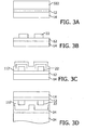
- Figures 3A to 3D illustrate manufacturing of a transparent layer stack or transparent body, which can for example be used for a touch panel display.
- the layer stack 12 is provided over the transparent substrate 14.
- the transparent substrate can be a flexible substrate or a rigid substrate, an organic substrate or an inorganic substrate, can be a glass or a foil, and can have other characteristics like being linearly or circular polarizing, a lambda quarter retarder or non-polarizing.
- the transparent substrate can have a high degree of transparency in the visible range of 380 nm to 780 nm.
- the transparent substrate 14 can include glass (flexible or rigid), plastic (flexible or rigid), which can further be already covered with thin film layers or hard coat, a linear or circular polarizer material, or lambda quarter retarder.
- glass substrates deposition processes and manufacturing methods on the glass substrate can be provided at higher temperatures as compared to plastic substrates. For example temperatures of 150°C or above or even temperatures of 200°C or above, such as 300 °C, can be utilized for manufacturing of transparent bodies for the touch panel display on glass substrates.
- the layer stack 12 is typically an index matching layer stack having at least a first and a second dielectric film, wherein the first refractive index is provided by the first electric film and the second refractive index is provided by the second dielectric film, and wherein the second refractive index is lower from the first refractive index.
- a first dielectric film, a second dielectric film and a plurality of further dielectric films can be deposited such that a continuous or quasi-continuous (e.g. step-like with small steps) change in refractive index can be generated in the transparent layer stack 12.
- the dielectric films can be manufactured by chemical vapor deposition or physical vapor deposition, for example sputtering or evaporation.
- Typical examples can be insulating materials with high and low refractive indexes, for example SiOx, MgF, TiOx, NbOx, SiNx, SiOxNy, AlOx, AlOxNy, TaOx, and combinations thereof.
- the transparent conductive layer stack has increased conductivity by providing an increased layer thickness or a decreased specific resistance of the layer material.
- TCO layer thicknesses of 40 nm and above, e.g. 50 nm to 150 nm can be utilized.
- the transparent conductive oxide layer can also be provided as a transparent conductive oxide layer stack having one or more transparent conductive oxide films.
- the transparent conductive oxide film or transparent conductive film stack can be heated during or after deposition, for example by thermal heating or by RTP flashlights.
- the transparent conductive oxide can be heated to temperatures of 80°C or above.
- the manufacturing of the transparent conductive oxide films can be provided by chemical vapor deposition or physical vapor deposition, e.g. sputtering or evaporation. In order to provide a high yield of manufacturing, for example DC sputtering of a transparent conductive oxide layer from a rotatable target can be provided.
- Typical examples of the transparent conductive oxide or the transparent conductive oxide layer stack can be ITO, doped ITO, , impurity-doped ZnO, In 2 O 3 , SnO 2 and CdO, ITO (In2O3:Sn), AZO (ZnO:Al), IZO (ZnO: In), GZO (ZnO:Ga), multi-component oxides including or consisting of combinations of ZnO, In 2 O 3 and SnO 2 , a layer stack from at least an ITO layer and a metal layer, e.g. an ITO/metal/ITO-stack or a metal/ITO/metal-stack.
- the transparent conductive oxide layer 322 (see figure 3A ) is structured to provide a structured transparent conductive oxide layer 22.
- the structured TCO layer can be provided by depositing a TCO layer and patterning the TCO layer in order to provide a structured TCO layer. Further, a mask and/or a photoresist can be provided to deposit the structured TCO layer.
- Figure 3C illustrates deposition of a second transparent layer stack 112 over the TCO structured TCO layer 22.
- the layer stack 112 is typically an index matching layer stack having at least a first dielectric film of the second transparent stack and a second dielectric film of the second transparent stack, wherein the first refractive index is provided by the first electric film and the second refractive index is provided by the second dielectric film, and wherein the second refractive index is lower from the first refractive index.
- a first dielectric film, a second dielectric film and a plurality of further dielectric films can be deposited in the second transparent layer stack such that a continuous or quasi-continuous (e.g. step-like with small steps) change in refractive index can be generated in the second transparent layer stack 112.
- the dielectric films can be manufactured by chemical vapor deposition or physical vapor deposition, for example sputtering or evaporation. Typical examples can be insulating materials with high and low refractive indexes, for example SiOx, TiOx, NbOx, SiNx, SiOxNy, AlOx, TaOx, and combinations thereof.
- Figure 3D illustrates a transparent adhesive 24, such as an optically clear adhesive in order to bond the transparent body to the display 34.
- the transparent adhesive can be an optical clear adhesive laminate or liquid optical clear adhesive with a refractive index close to a second substrate or polarizer, i.e. the substrate or polarizer of the display 34.
- the refractive index can be close to the refractive index of glass (1.48) or of PMMA (1.6), for example, in the range between 1.48 and 1.6.
- the transparent adhesive can have a visual transmittance of 95% or above, 97% or above , or even 99% or above.
- a structure TCO layer e.g. an ITO layer, two index matching layers and a transparent adhesive configured for bonding to a display, a color filter, an electro-optical device, or the like, is provided such that the two index matching layer on both sides of the TCO layer provide essentially invisibility of the structures of the TCO.
- the layer stack for example a touch panel layer stack or transparent body, can be bonded to or integrated in a display device with improved visual and electrical characteristics.
- layer stack or transparent body it is referred to layer stack or transparent body. It will be appreciated that these terms are used synonymously here, e.g. a transparent body is also provided by a stack of layers or films, i.e. a transparent body is also a layer stack.
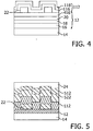
- Figure 4 illustrates yet further embodiments, which can be combined with other embodiments described herein.
- the substrate of the transparent body which can for example be used in a touch panel, is provided.
- the substrate can be, for example, the cover lens after the transparent touch body is bonded to an electro-optical device, such as a display or the like.
- the embodiments described with respect to figure 4 include four dielectric layers 16, 18, 20 and 416, which form a transparent layer stack.
- the structured transparent conductive film 22 is provided on top of the transparent layer stack.
- the transparent conductive oxide film can be TCO layer, which is deposited by DC sputtering from a rotatable target. However, other position techniques might be applied as well. Sputtering from a rotatable target is, for example useful for manufacturing of large area devices.
- large area substrates or respective carriers wherein the carriers have a plurality of substrates, may have a size of at least 0.174 m 2 .
- the size can be about 0.67m 2 (0.73x0.92m - Gen 4.5) to about 8 m 2 , more typically about 2 m 2 to about 9 m 2 or even up to 12 m 2 .
- the substrates or carriers, for which the structures, apparatuses, such as cathode assemblies, and methods according to embodiments described herein are provided are large area substrates as described herein.
- a large area substrate or carrier can be GEN 4.5, which corresponds to about 0.67 m2 substrates (0.73x0.92m), GEN 5, which corresponds to about 1.4 m 2 substrates (1.1 m x 1.3 m), GEN 7.5, which corresponds to about 4.29 m 2 substrates (1.95 m x 2.2 m), GEN 8.5, which corresponds to about 5.7m 2 substrates (2.2 m x 2.5 m), or even GEN 10, which corresponds to about 8.7 m 2 substrates (2.85 m x 3.05 m). Even larger generations such as GEN 11 and GEN 12 and corresponding substrate areas can similarly be implemented.
- the index matching layer stack 12 as shown in figure 4 , together with the second transparent layer stack having dielectric layers 116 and 118 results in improved optical characteristics.
- the structures of the TCO layer are essentially invisible to the user of such a device due to the two transparent layer stacks. According to embodiments described herein, this can be provided for the transparent conductive films having a sheet resistance of 100 Ohm/square or below, for example transparent conductive oxide layers of 20 nm or above, or even 100 nm or above. According to different embodiments, which can be combined with other embodiments described herein, two or more dielectric layers can be provided in the transparent layer stack 12
- the two or more layers can be a plurality of dielectric layers or films, for example, such that a gradient in the refractive index in the layer stack is provided.
- a first dielectric film can be provided with a first refractive index and the refractive index can be changed during further deposition of the transparent layer stack. The change can be continuous or step-like.
- further dielectric films (16-20; 416) can be provided, wherein a refractive index can be obtained in the transparent layer stack.
- the combination of the transparent layer stack 12 and the transparent conductive film can be repeated twice, three times or even four times.
- Figure 5 shows a transparent layer stack 12 deposited over the substrate 14.
- the structured transparent conductive film 22 is provided on the transparent layer stack 12.
- a second transparent layer stack 112 and a further transparent conductive film 522 are deposited.
- different refractive indices are provided for adjacent films.
- the second transparent conductive film 522 is provided over the second transparent layer stack 112.
- the cross-section illustrated in figure 5 does not show a structuring of the second transparent conductive film 522. However, the structuring can be applied in the direction different as compared to the paper plane.
- the transparent adhesive 24 is provided on the further transparent layer stack 512 and is configured for bonding the transparent body to the electro-optical device, such a display or the like.
- the first transparent layer stack, the transparent conductive film, and the second transparent layer stack 112 are deposited in a manner such that the a* and b* value for the manufactured transparent body is below 1.5 or, in particular 1, or more specifically, 0.7, or, even more specifically, 0.2.
- the a* and b* value for the structure formed solely by the first transparent layer stack, the transparent conductive film, and the transparent adhesive, and placed above a substantially transparent substrate may adopt these values.
- FIG. 6 shows a deposition apparatus 600.
- one vacuum chamber 602 for deposition of layers therein is shown.
- further chambers can be provided adjacent to the chamber 602.
- the vacuum chamber 602 can be separated from adjacent chambers by a valve having a valve housing 604 and the valve unit 605.
- the valve unit 605 can be closed.
- the atmosphere in the vacuum chambers can be individually controlled by generating a technical vacuum, for example with vacuum pumps connected to the chamber 602, and/or by inserting process gases in the deposition region in the chamber.
- process gases can include inert gases such as argon and/or reactive gases such as oxygen, nitrogen, hydrogen and ammonia (NH3), Ozone (03), or activated gases or the like.
- inert gases such as argon and/or reactive gases such as oxygen, nitrogen, hydrogen and ammonia (NH3), Ozone (03), or activated gases or the like.
- reactive gases such as oxygen, nitrogen, hydrogen and ammonia (NH3), Ozone (03), or activated gases or the like.
- the groups of deposition sources 622 and 624 are illustrated in FIG. 6 .
- the groups of deposition sources can typically be provided in different chambers in the event different deposition processes are provided by the groups of deposition sources.
- the deposition sources can for example be rotatable cathodes having targets of the material to be deposited on the substrate.
- the cathodes can be rotatable cathodes with a magnetron therein. Thereby, magnetron sputtering can be conducted for depositing of the layers.
- Cathodes 622 are connected to an AC power supply 623 such that the cathodes can be biased in an alternating manner.
- magnet sputtering refers to sputtering performed using a magnet assembly, that is, a unit capable of a generating a magnetic field.
- a magnet assembly consists of a permanent magnet.
- This permanent magnet is typically arranged within a rotatable target or coupled to a planar target in a manner such that the free electrons are trapped within the generated magnetic field generated below the rotatable target surface.
- Such a magnet assembly may also be arranged coupled to a planar cathode.
- magnetron sputtering can be realized by a double magnetron cathode, i.e. cathodes 622, such as, but not limited to, a TwinMagTM cathode assembly.
- cathodes 622 such as, but not limited to, a TwinMagTM cathode assembly.
- target assemblies including double cathodes can be applied.
- the cathodes in a deposition chamber may be interchangeable. Accordingly, the targets are changed after the silicon has been consumed.
- that dielectric layers can be deposited by sputtering, for example magnetron sputtering, of rotatable cathodes having an AC power supply.
- MF sputtering can be applied for depositing the dielectric layers.
- sputtering from a silicon target e.g. a sprayed silicon target
- MF sputtering that is middle frequency sputtering.
- middle frequency is a frequency in the range 5 kHz to 100 kHz, for example, 10 kHz to 50 kHz.
- Sputtering from a target for a transparent conductive oxide film is typically conducted as DC sputtering.
- the cathodes 624 are connected to the DC power supply 626 together with anodes 625 collecting electrons during sputtering.
- the transparent conductive oxide layers for example the ITO layers, can be sputtered by DC sputtering, i.e. an assembly having cathodes 624.
- the cathodes 622 and 624 are illustrated to be provided in one vacuum chamber 602.
- the cathodes for depositing different layers are provided in different vacuum chamber, for example the chamber 602 and the vacuum chambers adjacent to the vacuum chamber 602, as illustrated by the lower cathodes 622 in FIG. 6 .
- the dielectric layers, as described herein, which can be oxide-layers, nitrite-layers, or oxinitride-layers can be deposited by a reactive deposition process where the target material reacts with oxygen and/or nitrogen after the material has been released from the target.
- an atmosphere with an appropriate processing gas and/or the appropriate degree of technical vacuum can be provided in each deposition area.
- two or more groups of cathodes 622 can be provided in the deposition apparatus 600.
- deposition is performed by sputtering of one or more rotatable targets. More specifically, according to embodiments herein, at least one of the films referred to above is deposited by sputtering of a rotatable target, so that formation of a stable transparent body and with a high quality is facilitated.
- a film may be deposited having a higher uniformity, and with a low density of defects and contamination particles. Thereby, it is facilitated manufacturing of a high-quality transparent body that not only yields a proper transmission of light but also yields a stable performance over time.
- a manufacturing process including sputtering of one or more rotatable targets may further facilitate a higher manufacturing rate and the production of a lower number of contaminant particles as compared to other deposition methods.
- Figure 7 shows a flowchart 700 illustrating a process for manufacturing a transparent body as described herein.
- the first transparent layer stack e.g. layers stack 12
- the layer stack includes at least two dielectric films, wherein the refractive indices of the dielectric films are different from each other and films with a higher refractive index and films with the lower refractive index can be deposited in an alternating manner.
- the structured transparent conductive film for example structured ITO layer, is deposited over the transparent layer stack 12.
- the structured transparent conductive film can be also a stack of conductive films.
- a TCO/metal/TCO-stack can be provided in step 704.
- structuring procedures can be selected from the group consisting of: (1) laser scribing, (2) photo lithography, (3) printing adsorption barrier pattern (e.g. oil) followed by TCO deposition, (4) a lift-off process (formation of photo-resist pattern on substrate followed by TCO deposition and lift-off with photo-resist solvent), (5) film deposition using a shadow mask, or combinations thereof.
- adsorption barrier pattern e.g. oil
- lift-off process formation of photo-resist pattern on substrate followed by TCO deposition and lift-off with photo-resist solvent
- film deposition using a shadow mask or combinations thereof.
- one or some of the chambers may be configured for performing sputtering without a magnetron assembly.
- One or some chambers, for example additional chamber, may be configured for performing deposition by other methods, such as, but not limited to, chemical vapor deposition or pulsed laser deposition.
- the deposition apparatuses as described herein can further include a measurement system 638 configured for measuring during deposition optical properties of at least one of the films forming part of at least one of the first layer stack or the transparent conductive film.
- the dielectric films can be typically reactively sputtered.
- the first deposition assembly (622) can be configured for depositing the dielectric films by reactive sputtering.
- Si-containing layers or A1 containing layers can be sputtered reactively, and/or Nb-containing layers, Ti-containing layers or ITO-containing layers can be sputtered from a ceramic target.
- exemplary process 700 may further include a heating treatment of the substrate for degassing of the substrate prior to deposition.
- the substrate may be heated at a temperature between 60 and 360 °C depending on the substrate speed.
- exemplary process 700 may include performing a DC and/or medium frequency (MF) pre-treatment of the substrate with a power between 1 and 3 kW.
- exemplary process 700 may include performing a pre-treatment of the substrate at an argon and/or oxygen atmosphere such as, for example, an oxygen rich pre-treatment.
- medium frequency is a frequency in the range of 5 kHz to 100 kHz, for example, 30 kHz to 50 kHz.
- the sputter coating sources in the exemplary deposition apparatuses or in an apparatus according to embodiments herein may be a DC-cathode with planar or rotatable targets (such as, but not limited to, ceramic ITO), and planar or rotatable targets (such as a doped silicon target, in particular sprayed Si targets for depositing SiO 2 , or Si3N4, SiOxNy) or targets including a material to deposit one of the other dielectric layers disclosed herein.
- planar or rotatable targets such as, but not limited to, ceramic ITO
- planar or rotatable targets such as a doped silicon target, in particular sprayed Si targets for depositing SiO 2 , or Si3N4, SiOxNy
- the transparent conductive film has a sheet resistance of 100 Ohm/square or below.
- This can be provided by providing a comparably thick transparent conductive layer and/or utilizing a TCO material with a low specific resistivity. This results in a more complex index-matching situation for reaching the required high optical performance such as pattern invisibility, color neutrality and high transmittance levels.
- a second transparent layer stack e.g., layers stack 12
- the layer stack includes at least two dielectric films, wherein the refractive indices of the dielectric films are different from each other and films with a higher refractive index and films with the lower refractive index can be deposited in an alternating manner.
- a transparent adhesive for example an optically clear adhesive, is provided in order to bond the transparent body to an electro-optical device, such as a display, a display of a mobile phone, a display of the touch panel TV, a display of the touch panel computer, or the like.
- the transparent body i.e. the thin film stacks
- the transparent body are produced involving magnetron sputtering from rotary targets.
- invisible ITO solutions have extremely high demands on the optical uniformity of optical properties (color values in transmission and reflection), which corresponds technically to the deposition of very uniform films with respect to film thickness and optical dispersion properties. Accordingly, longer targets than the targeted sputtering height can be utilized.
- planar targets have-deposition zones, which are responsible for enhanced particle generation, and hence need to be much longer than rotary targets to provide for particle-free and uniform films.
Description
- Embodiments of the present disclosure relate to processes and systems for manufacturing a transparent body for use in a touch panel and a transparent body fabricated according to these processes.
- Touch panels are a particular class of electronic visual displays, which are able to detect and locate a touch within a display area. Generally, touch panels include a transparent body disposed over a screen and configured to sense a touch. Such a body is substantially transparent, so that light in the visible spectrum emitted by the screen can be transmitted therethrough. At least some known touch panels include a transparent body constituted by a barrier and a transparent conductor formed, in this order, over a substrate. A touch on the display area of such a panel generally results in a measurable change of capacitance in a region of the transparent body. The change in capacitance may be measured using different technologies, so that the position of the touch can be determined.
- A transparent body for use with a touch panel is subject to some particular requirements. In particular, one key requirement is that the transparent body is stable enough for withstanding multiple contacts on the screen and harsh conditions, so that reliability of the touch screen is not compromised over time. However, at least some known transparent bodies included in touch screens, which are considered robust interfere with a proper transmission of light therethrough due to, for example, thickness, composition, and structure of the layers forming the transparent body. Furthermore, fabricating such a stable transparent body with high quality, for example with a uniform and defect-free barrier, is challenging.
- Further, it is to be considered that there are different types of transparent bodies for touch panels. Particular consideration of the optical characteristics, e.g. the appearance to a user, has to be taken into account for transparent bodies, wherein the conductive layer for measuring the change in capacitance is a structured conductive layer.
- A further aspect to be considered is the steadily increasing size of displays, wherein beyond the optical characteristics described above, also electrically characteristics are of increasing interest. Thereby, a design of thin film based flat panel displays and touch screen technologies, which provides an invisible object, which is patterned with respect to conductivity (like a touch sensor structure) and which exhibits enhanced optical and electrical performance compared to conventional structures, is desired.
- Accordingly, it is desirable a process and an apparatus for forming a high-quality transparent body for use in a touch panel in a manner such that the body is stably formed over the substrate without compromising a proper transmission of light in the visible spectrum and improved electrical characteristics.
-
EP2402481A1 andEP1574882A1 describe methods of manufacturing touch screen panels. - In light of the above, the invention provides a process according to
independent claim 1, a transparent body according to independent claim 7, and an apparatus according toindependent claim 15. Further aspects, advantages, and features of the present invention are apparent from the dependent claims, the description, and the accompanying drawings. - According to one embodiment, a process for manufacturing a transparent body for use in a touch panel is provided. The process includes optionally depositing a first transparent layer stack over a transparent substrate, wherein said first transparent layer stack includes at least a first dielectric film with a first refractive index, and a second dielectric film with a second refractive index different from the first refractive index. The process includes; depositing a structured transparent conductive film over the first transparent layer stack, wherein the structured transparent conductive film corresponding to a sheet resistance of 100 Ohm/square or below; depositing a second transparent layer stack over the transparent conductive film, wherein said second transparent layer stack includes at least a third dielectric film with a third refractive index, and a fourth dielectric film with a fourth refractive index different from the third refractive index, wherein the first transparent layer stack if provided, the structured transparent conductive film and the second transparent layer stack are provided in this order. According to an alternative embodiment, a transparent adhesive having a fourth refractive index different from the third refractive index can be provided instead of the fourth dielectric film.
- According to another embodiment, a transparent body adapted for use in a touch panel is provided. The transparent body includes a transparent substrate, and optionally a first transparent layer stack deposited over the transparent substrate, wherein said transparent layer stack includes at least a first dielectric film with a first refractive index, and a second dielectric film with a second refractive index different from the first refractive index. The layer stack includes a transparent conductive film deposited over the first transparent layer stack, wherein the structured transparent conductive film has a sheet resistance of 100 Ohm/square or below, and a second transparent layer stack deposited over the transparent conductive film, wherein said second transparent layer stack includes at least a third dielectric film with a third refractive index, and a fourth dielectric film with a fourth refractive index different from the third refractive index. According to an alternative embodiment, a transparent adhesive having a fourth refractive index different from the third refractive index can be provided instead of the fourth dielectric film.
- According to another embodiment, a deposition apparatus for manufacturing a transparent body for use in a touch panel is provided. The apparatus includes a first deposition assembly configured to deposit a first transparent layer stack over a substrate, said first transparent layer stack including at least first dielectric film with a first refractive index, and a second dielectric film with a second refractive index different from the first refractive index, a second deposition assembly configured to deposit a transparent conductive film, and a third deposition assembly configured to deposit a second transparent layer stack over the transparent conductive film, said second transparent layer stack including at least third dielectric film with a third refractive index, and a fourth dielectric film with a fourth refractive index different from the third refractive index, wherein said first deposition assembly, said second deposition assembly, and the third deposition assembly are arranged such that the first transparent layer stack, the transparent conductive film and the second transparent layer stack are disposed over the substrate in this order, and wherein at least one of the first deposition assembly or the second deposition assembly or the third deposition assembly inlcudes a sputtering system operatively coupled to a target, said sputtering system being configured to deposit at least one of the first dielectric film, the second dielectric film, the third dielectric film, the fourth dielectric film or the transparent conductive film by sputtering of the target.
- Surprisingly, the combination of dielectric films deposited according to embodiments of the present disclosure having additional dielectric films in comparison to at least some known transparent bodies for use in a touch panel, with a characteristic combination of refractive indexes in combination with second transparent layer stack of dielectric films, and in which at least one of the films is deposited by sputtering of a target, facilitates manufacturing of a high-quality transparent body that not only yields proper transmission of light but also yields stable performance over time. Yet further, as compared to existing "invisible" layer stacks or transparent bodies for touch panels, the resistance can be reduced, which is, for example, useful for large area touch panels.
- Embodiments are also directed to apparatuses for carrying out the disclosed processes and including apparatus parts for performing described process steps. Furthermore, embodiments are also directed to methods by which the described apparatus operates or by which the described apparatus is manufactured. The methods may include method steps for carrying out functions of the apparatus or manufacturing parts of the apparatus. The method steps may be performed by way of hardware components, firmware, software, a computer programmed by appropriate software, by any combination thereof or in any other manner.
- A full and enabling disclosure, including the best mode thereof, to one of ordinary skill in the art, is set forth more particularly in the remainder of the specification, including reference to the accompanying figures, wherein:
-
Fig. 1A is a schematic representation of an exemplary transparent body for use in a touch panel in accordance with embodiments herein; -
Fig. 1B is a schematic representation of an exemplary transparent body for use in a touch panel in accordance with embodiments herein; -
Fig. 2 is a schematic representation of a further exemplary transparent body for use in a touch panel and an opto-electronic device to which the body is bonded in accordance with embodiments herein; -
Figs. 3A to 3D are schematic representation of the manufacturing of an exemplary transparent body for use in a touch panel in accordance with embodiments herein; -
Figs. 4 and 5 are schematic representations of yet further exemplary transparent bodies for use in a touch panel in accordance with embodiments herein; -
Fig. 6 is a schematic representation of a portion of an apparatus for depositing an exemplary transparent body for use in a touch panel in accordance with embodiments herein; and -
Fig. 7 is a flow chart illustrating methods of manufacturing a transparent body for use in a touch panel in accordance with embodiments herein. - Reference will now be made in detail to the various embodiments, one or more examples of which are illustrated in the figures. Each example is provided by way of explanation, and is not meant as a limitation of the invention. It is contemplated that elements of one embodiment may be advantageously utilized in other embodiments without further recitation.
- According to embodiments herein, a first
transparent layer stack 12, as depicted inFIG. 1A , is deposited over asubstrate 14. The term "substrate" as used herein shall embrace both inflexible substrates, e.g., a wafer, slices of transparent crystal such as sapphire or the like, or a glass plate, and flexible substrates such as a web or a foil. The term "transparent" as used herein shall particularly include the capability of a structure to transmit light with relatively low scattering, so that, for example, light transmitted therethrough can be seen in a substantially clearly manner. In the case of a flexible substrate, it is typical thatsubstrate 14 has ahard coat 15 formed thereon. - According to typical embodiments, a layer stack is constituted by a number of films formed (e.g., by deposition) one atop of another. In particular, embodiments herein include depositing a first transparent layer stack which may be constituted by a plurality of dielectric films, that is, films that, substantially, do not conduct electricity. In particular, first
transparent layer stack 12 may include a firstdielectric film 16, and a seconddielectric film 18, as exemplarily depicted inFIG. 1A . Thereby, the first transparent layer stack may constitute a barrier for use in a touch panel. - As shown in
FIG. 1A , a structured transparent conductive oxide (TCO)film 22 is provided over the transparent layer stack. According to typical embodiments, the structured TCO layer can be provided by depositing a TCO layer and patterning the TCO layer in order to provide a structured TCO layer. Alternatively, a mask and/or a photoresist can be provided to deposit the structured TCO layer. - According to typical embodiments, which can be combined with other embodiments described herein, the transparent conductive oxide layer can be an indium tin oxide (ITO) layer, a doped ITO layer, impurity-doped ZnO, In2O3, SnO2 and CdO, ITO (In2O3:Sn), AZO (ZnO:Al), IZO (ZnO: In), GZO (ZnO:Ga), multi-component oxides including or consisting of combinations of ZnO, In2O3 and SnO2, a layer stack from at least an ITO layer and a metal layer, e.g. an TTO/metal/ITO-stack or a metal/ITO/metal-stack.
- Conventional layer stacks or transparent bodies for touch panels can result in a functional screen (like a touch screen). However, an inferior sunlight readability, a colored appearance (reflectance) of the screen and a color change with respect to the produced picture from the underlying display, and a more or less visible pattern from the structured core layer of the functional screen (e.g. a patterned transparent conductive oxide, TCO) is often obtained. Further, the conductivity might not be sufficient for large area touch panels, e.g. touch panels with a size of diagonal 7 inch or above, specifically for touch screens with a diagonal of more than 20 inch.
- Due to the structure of the transparent layer stack, it is facilitated that the conductive film does not prejudice an optimal transmission of light through the body. In particular, a transparent layer stack according to embodiments herein facilitates that a conductive film, even a structured conductive film, does not affect the neutrality of the reflectance color, as further discussed below.
- According to typical embodiments, which can be combined with other embodiments described herein, the sheet resistance of the structured TCO layer is 100 Ohm/sq and below, e.g. 10 to 50 Ohm/sq. Typically, the sheet resistance is the physical quantity referred to in this context, even though this value refers to the resistance of a layer with a sufficiently large area, i.e. without too small patterns. The structured TCO pattern, e.g. lines corresponds to a line resistance in Ohm. However, the sheet resistance is the relevant parameter and can be determined by deposition of test areas or can be determined or calculated based upon the resistance of patterned structures and the structure geometry. Accordingly, even though the sheet resistance of the structure layer can not be directly determined (yet indirectly) and rather refers to the resistance of a unstructured layer, a person skilled in the art would relate to a sheet resistance corresponding to a value for the structured layer.
- According to different embodiments, the TCO films, e.g. ITO, can be deposited at relatively high temperatures or alternatively at lower temperatures, wherein in the latter case an annealing step after deposition can be provided in order to achieve desired layer characteristics such as the sheet resistance.
- Thereby, for example, TCO layer thicknesses of 20 nm or above, e.g. 50 nm to 150 nm can be utilized. Additionally or alternatively, transparent conductive oxides with a with a specific resistance lower than the typical resistivity range of ITO produced with various process schemes, which is 130-450 µΩcm for bulk ITO i.e. superior electrical characteristics, but with inferior optical characteristics could be used. The reduced sheet resistance and/or the increased TCO layer thickness results in the desire for further improvement of the layer stack, as the, e.g. thicker, structured TCO layer tends to be more easily visible.
- According to embodiments described herein, an enhanced structure and method of manufacturing such an invisible object, e.g. a touch sensor, are provided to surpass limitations to the patterned TCO thickness and its conductivity. Layer stacks or transparent bodies, as described herein, which are provided on a display, or the like are considered invisible when placed in an atmosphere of air (refractive index 1) with very little difference in the optical appearance between areas with and without the TCO layer, such as ITO ("invisible" ITO). According to some embodiments, which can be combined with other embodiments described herein, different stacks and mounting scheme for an invisible object, e.g. for being integrated into or mounted onto a display in such a way, that at least on one side of the object the adjacent medium has a refractive index being different than 1, e.g. 1.3 to 1.7. By this means, the invisible stack can support a sheet resistance of 20 Ohm/sq or below, which is an improvement by a factor of 10 compared to the previous concepts without compromising on optical performance.
- As shown in
FIG. 1A a secondtransparent layer stack 112 is provided over theTCO layer 22. According to typical embodiments, a second layer stack is constituted by a number of films formed (e.g., by deposition) one atop of another. In particular, embodiments herein include depositing a second transparent layer stack, which may be constituted by a plurality of dielectric films, that is, films that, substantially, do not conduct electricity. In particular, secondtransparent layer stack 112 may include a thirddielectric film 116, and afourth dielectric film 118, as exemplarily depicted inFIG. 1A . Thereby, an improved index matching can be provided. Further, a passivation of the below TCO layer can be provided. Further, an overall transmittance can be provided as compared to an uncoated substrate. - According to typical embodiments described herein, which can be combined with other embodiments described herein, the
first dielectric film 16 of the firsttransparent layer stack 12, i.e. the first transparent dielectric film over the substrate is a high refractive index film, e.g. with a refractive index of 1.8 or above. According to yet further alternative or additional modifications, the transparent conductive oxide layer is provided between, e.g. directly between, a low refractive index (1.5 or below) dielectric film and a high refractive index (1.8 or above) dielectric film. Further, additionally or alternatively, the last dielectric film over the substrate can be a low refractive index dielectric film. Thereby, the last dielectric film is referred to as the last dielectric film of the touch panel transparent body, i.e. before a transparent adhesive or air gap is provided at a bonding interface to a color filter, a second substrate or an opto-electronic device. - As compared to previous designs of touch panel displays where, particularly for layer stacks or transparent bodies with thicker TCO layers, an air gap has been provided, embodiments described herein provide a layer stack or transparent body having at least a first index matching layer stack, e.g. one or more dielectric films, a TCO layer over the index matching layer stack, wherein the TCO layer has a sheet resistance of 100 Ohm/sq or below, and a second index matching layer stack. A transparent adhesive can be provided onto transparent body, i.e. in contact with the transparent body according to embodiments described herein. Even though, an air gap might be used for mounting the herein described embodiments of a transparent body to an opto-electronic device, also an optical clear adhesive can be used. The embodiments thereby provide an "invisible" touch panel structure, which also provides for a low resistance. The second transparent layer stack for sandwiching the TCO between two transparent layer stacks and for obtaining a solution to low-resistance "invisible" TCO patterns refer to a structure having a TCO layer on top before this structure is bonded, e.g. optically bonded, onto the adjacent components of a touch screen display with a transparent adhesive. By utilizing the second transparent layer stack, a final pattern "invisibility" of the TCO pattern can be achieved.
- According to embodiments herein, a first
transparent layer stack 12, as depicted inFIG. 1B , is deposited over asubstrate 14. In the case of a flexible substrate, it is typical thatsubstrate 14 has ahard coat 15 formed thereon. - According to typical embodiments, the
layer stack 12 and the structured transparentconductive film 22 can be provided similar to the embodiments described with respect toFIG. 1A . - As shown in
FIG. 1B a secondtransparent layer stack 112 is provided over theTCO layer 22. According to typical embodiments, a second layer stack is constituted by a number of films or layers formed (e.g., by deposition) one atop of another. In particular, secondtransparent layer stack 112 may include a thirddielectric film 116, and atransparent adhesive 24, with a refractive index different from the third dielectric film such that an index matching is provided. - According to typical embodiments described herein, which can be combined with other embodiments described herein, the
first dielectric film 16 of the firsttransparent layer stack 12, i.e. the first transparent dielectric film over the substrate is a high refractive index film, e.g. with a refractive index of 1.8 or above. According to yet further alternative or additional modifications, the transparent conductive oxide layer is provided between, e.g. directly between, a low refractive index (1.5 or below) dielectric film and a high refractive index (1.8 or above) dielectric film. - As compared to previous designs of touch panel displays where, particularly for layer stacks with thicker TCO layers, an air gap has been provided, embodiments described herein provide a layer stack having at least a first index matching layer stack, e.g. one or more dielectric films, a TCO layer over the index matching layer stack, wherein the TCO layer has a sheet resistance of 100 Ohm/sq or below, and a second index matching layer stack. A transparent adhesive can be provided onto transparent body, i.e. in contact with the transparent body according to embodiments described herein. As illustrated with respect to
FIGS. 1A and 1B , the transparent adhesive can be part of the second index matching layer stack or can be provided mainly for bonding purposes, e.g. by having a fourth dielectric film. - Even though, an air gap might be used for mounting the herein described embodiments of a transparent body to an opto-electronic device, also an optical clear adhesive can be used. The embodiments thereby provide an "invisible" touch panel structure, which also provides for a low resistance. The second transparent layer stack for sandwiching the TCO between two transparent layer stacks and for obtaining a solution to low-resistance "invisible" TCO patterns refer to a structure having a TCO layer on top before this structure is bonded, e.g. optically bonded, onto the adjacent components of a touch screen display with a transparent adhesive. By utilizing the second transparent layer stack, a final pattern "invisibility" of the TCO pattern can be achieved.
- As shown in
FIG. 2 , atransparent adhesive 24 is provided to bond the touch panel layer stack or transparent body having, e.g., asubstrate 14, alayer stack 12, astructure TCO layer 22, and asecond layer stack 112 to a display. InFig. 2 , the display is examplarily indicated by acolor filter 32 and a pixel array ordisplay 34. Thereby, thetransparent body 10 is shown inverted as compared toFIG. 1A . Accordingly, thesubstrate 14 can be, for example, a cover lens of a touch panel display. The term cover lens is typically used as a topmost glass of a touch panel. According to yet further embodiments, which can be combined with other embodiments described herein, thetransparent body 10 can be bonded with the transparent adhesive, for example an OCA (optical clear adhesive), to a color filter glass, to a polarizer of a display structure, or to a liquid crystal display structure itself. - Embodiments according to the present invention relate to a layer stack or transparent body comprising of a substrate, e.g. a cover glass, and a stack of multiple layers that is mounted on top of a display with a clear adhesive, i.e. without an air gap. The first and second layer stacks include transparent, insulating materials with high and low refractive indexes (such SiOx, TiOx, NbOx, SiNx, SiOxNy, AlOxNy, MgF2, TaOx) and transparent conductive materials, like transparent conductive oxides, for example ITO. According to implementations, the method of layer coating or layer deposition can be chemical or physical vapor deposition.
- According to an example, a layer stack or transparent body can be manufactured as follows, wherein improved visual invisibility and color fastness within the final TSP (touch screen panel)/display product and reduced electrical resistance can be provided. The layers are numbered as they are subsequently deposited on a substrate, e.g. a cover lens such as a glass having a thickness of 0.1 mm or above, e.g. of 0.5 mm: Layer 1: Nb2O5 of 5-200 nm thickness, e.g. of 8 nm. Layer 2: SiO2 of 20-150 nm thickness, e.g. of 35 nm thickness, Layer 3: ITO of 20-200 nm thickness, e.g. of 150 nm thickness, wherein a patterning after deposition is conducted. Typically, the ITO layer can be deposited, e.g. by sputtering from a rotatable target, at a substrate temperature of 300°C. Layer 4: Nb2O5 of 5-200 nm thickness, e.g. of 100 nm Layer 5: SiO2 of 20-150, e.g. of 87 or 90 nm. For example, the ITO thickness used for a touch sensor provides for very low sheet resistance of 15 Ohm/sqr or below. The reflection of the coated substrate is below 5% and the reflection difference between the area with and without ITO is below 0.2%. The visual transmission TY is above 92%. The optical color difference between areas with and without ITO, dE*ab is below 0.9. The layer stack or transparent body including the substrate has a neutral color for areas with and without ITO in reflection and transmission, e.g., |a*| and |b*| are both below 1.0.
- According to typical embodiments, which can be combined with other embodiments described herein, the first dielectric film being deposited on the substrate can typical be a high refractive index layer, e.g. with a refractive index of at least 1.8 For example, a niobium-oxide containing film can be deposited as the first dielectric film on the substrate.
- According to yet further embodiments, which can be combined with other embodiments described herein, a TCO thickness of below 145 nm, e.g. of 20 nm to 130 nm, such as 75 nm, will result in even better invisibility characteristics as the above described values.
- According to a further different example, a layer stack or transparent body can be manufactured as follows, wherein improved visual invisibility and color fastness within the final TSP (touch screen panel)/display product and reduced electrical resistance can be provided. The layers are numbered as they are subsequently deposited on a substrate, e.g. a cover lens such as a glass having a thickness of 0.1 mm or above, e.g. of 0.5 mm: Layer 1: Nb2O5 of 5-200 nm thickness, e.g. of 8 nm. Layer 2: SiO2 of 20-150 nm thickness, e.g. of 31 nm thickness, Layer 3: ITO of 30-70 nm thickness, e.g. of 40 nm thickness, wherein a patterning after deposition is conducted. Typically, the ITO layer can be deposited, e.g. by sputtering from a rotatable target, at a substrate temperature of 300°C. Layer 4: Nb2O5 of 5-200 nm thickness, e.g. of 98 nm Layer 5: SiO2 of 20-150 nm, e.g. of 87 or 90 nm. For example, the ITO thickness used for a touch sensor provides for very low sheet resistance of 50 Ohm/sqr or below. The reflection of the coated substrate is below 5% and the reflection difference between the area with and without ITO is below 0.4 %. The visual transmission TY is above 94%. The optical color difference between areas with and without ITO, dE*ab is below 1.3. The layer stack or transparent body including the substrate has a neutral color for areas with and without ITO in reflection and transmission, e.g., |a*| and |b*| are both below 1.0.
- According to a yet further different example, a layer stack or transparent body can be manufactured as follows, wherein improved visual invisibility and color fastness within the final TSP (touch screen panel)/display product and reduced electrical resistance can be provided. The layers are numbered as they are subsequently deposited on a substrate, e.g. a cover lens such as a glass having a thickness of 0.1 mm or above, e.g. of 0.5 mm: Layer 1: Nb2O5 of 5-200 nm thickness, e.g. of 9 nm. Layer 2: SiO2 of 20-150 nm thickness, e.g. of 28 nm thickness, Layer 3: ITO of 40-80 nm thickness, e.g. of 60 nm thickness, wherein a patterning after deposition is conducted. Typically, the ITO layer can be deposited, e.g. by sputtering from a rotatable target, at a substrate temperature of 300°C. Layer 4: Nb2O5 of 5-200 nm thickness, e.g. of 98 nm Layer 5: SiO2 of 20-150 nm, e.g. of 89 nm. For example, the ITO thickness used for a touch sensor provides for very low sheet resistance of 30 Ohm/sqr or below. Similar values as described above can be provided with the yet further example.
- According to a yet further different example, a layer stack or transparent body can be manufactured as follows, wherein improved visual invisibility and color fastness within the final TSP (touch screen panel)/display product and reduced electrical resistance can be provided. The layers are numbered as they are subsequently deposited on a substrate, e.g. a cover lens such as a glass having a thickness of 0.1 mm or above, e.g. of 0.5 mm: Layer 1: Nb2O5 of 5-200 nm thickness, e.g. of 7 nm. Layer 2: SiO2 of 20-150 nm thickness, e.g. of 23 nm thickness, Layer 3: ITO of 20-80 nm thickness, e.g. of 45 nm thickness, wherein a patterning after deposition is conducted. Typically, the ITO layer can be deposited, e.g. by sputtering from a rotatable target, at a substrate temperature of 300°C. Layer 4: SiO2 of 20-150 nm, e.g. of 23 nm Layer 5: Nb2O5 of 5-50 nm thickness, e.g. of 7 nm Similar values as described above can be provided with the yet further example.
- Accordingly, in light of the above, according to some embodiments, which can be combined with other embodiments described herein, the fourth refractive index, e.g. of layer 5 above, can be higher than the third refractive index, e.g. of layer 4 above.
- According to yet further typical embodiments, the
dielectric films - More specifically, according to embodiments herein, the second, optionally a fourth dielectric film or further dielectric films can be a film, e.g. consisting of SiO2 have a lower refractive index than the first dielectric film, e.g. consisting of Nb2O5, Si3N4 or the like. A first transparent layer stack of a transparent body, e.g. a two-layer-type stack, and a second transparent layers stack, e.g. a two-layer-type stack, manufactured according to embodiments herein provides, in view of the additional dielectric films in comparison to at least some known transparent bodies for use in a touch panel and the characteristic combination of films with different refractive indexes, a barrier that facilitates a proper transmission of light through the transparent body. According to typical embodiments, which can be combined with other embodiments described herein, dielectric films with lower refractive index, for example lower than 1.50 or, more specifically, lower than 1.47 or, even more specifically, lower than 1.45 and dielectric films with higher refractive index, for example of at least 1.80 or, more specifically, at least 2.10, or, even more specifically, at least 2.40 are provided in an alternating manner. Thereby, films having lower refractive indexes can be provided by films containing SiOx, MgF, SiOxNy, or the like. For example, films having a higher refractive index can be provided by films containing NbOx, SiNx, SiOxNy, TiOx AlOx, AlOxNy, TaOx, or the like.
- According to embodiments described herein,
transparent body 10 includes a transparentconductive film 22, such as, but not limited to, indium tin oxide (ITO), in particular, crystalline ITO or ITO with a sheet resistance of 100 Ohm/square and below. According to different embodiments, which can be combined with other embodiments described herein, typically, ITO with composition 97% In2O3 and 3% SnO2 for crystalline ITO and/or ITO with composition 90% In2O3 and 10% SnO2 for non-crystalline ITO can be used. -
Figures 3A to 3D illustrate manufacturing of a transparent layer stack or transparent body, which can for example be used for a touch panel display. As shown infigure 3A , thelayer stack 12 is provided over thetransparent substrate 14. According to different embodiments, the transparent substrate can be a flexible substrate or a rigid substrate, an organic substrate or an inorganic substrate, can be a glass or a foil, and can have other characteristics like being linearly or circular polarizing, a lambda quarter retarder or non-polarizing. Typically, the transparent substrate can have a high degree of transparency in the visible range of 380 nm to 780 nm. - According to yet further examples, the
transparent substrate 14 can include glass (flexible or rigid), plastic (flexible or rigid), which can further be already covered with thin film layers or hard coat, a linear or circular polarizer material, or lambda quarter retarder. Particularly for glass substrates, deposition processes and manufacturing methods on the glass substrate can be provided at higher temperatures as compared to plastic substrates. For example temperatures of 150°C or above or even temperatures of 200°C or above, such as 300 °C, can be utilized for manufacturing of transparent bodies for the touch panel display on glass substrates. - According to yet further embodiments, which can be combined with other embodiments described herein, the
layer stack 12 is typically an index matching layer stack having at least a first and a second dielectric film, wherein the first refractive index is provided by the first electric film and the second refractive index is provided by the second dielectric film, and wherein the second refractive index is lower from the first refractive index. According to an exemplary implementation, which can be combined with other embodiments described herein, a first dielectric film, a second dielectric film and a plurality of further dielectric films can be deposited such that a continuous or quasi-continuous (e.g. step-like with small steps) change in refractive index can be generated in thetransparent layer stack 12. According to typical implementations, the dielectric films can be manufactured by chemical vapor deposition or physical vapor deposition, for example sputtering or evaporation. Typical examples can be insulating materials with high and low refractive indexes, for example SiOx, MgF, TiOx, NbOx, SiNx, SiOxNy, AlOx, AlOxNy, TaOx, and combinations thereof. - As shown in
figure 3A a transparentconductive oxide layer 322 is deposited over thelayer stack 12. According to embodiments described herein, the transparent conductive layer stack has increased conductivity by providing an increased layer thickness or a decreased specific resistance of the layer material. Thereby, for example, TCO layer thicknesses of 40 nm and above, e.g. 50 nm to 150 nm can be utilized. - According to yet further embodiments, which can be combined with other embodiments described herein, the transparent conductive oxide layer can also be provided as a transparent conductive oxide layer stack having one or more transparent conductive oxide films. During manufacturing, the transparent conductive oxide film or transparent conductive film stack can be heated during or after deposition, for example by thermal heating or by RTP flashlights. Typically, the transparent conductive oxide can be heated to temperatures of 80°C or above. The manufacturing of the transparent conductive oxide films can be provided by chemical vapor deposition or physical vapor deposition, e.g. sputtering or evaporation. In order to provide a high yield of manufacturing, for example DC sputtering of a transparent conductive oxide layer from a rotatable target can be provided. Typical examples of the transparent conductive oxide or the transparent conductive oxide layer stack can be ITO, doped ITO, , impurity-doped ZnO, In2O3, SnO2 and CdO, ITO (In2O3:Sn), AZO (ZnO:Al), IZO (ZnO: In), GZO (ZnO:Ga), multi-component oxides including or consisting of combinations of ZnO, In2O3 and SnO2, a layer stack from at least an ITO layer and a metal layer, e.g. an ITO/metal/ITO-stack or a metal/ITO/metal-stack.
- As shown in
figure 3B , the transparent conductive oxide layer 322 (seefigure 3A ) is structured to provide a structured transparentconductive oxide layer 22. The structured TCO layer can be provided by depositing a TCO layer and patterning the TCO layer in order to provide a structured TCO layer. Further, a mask and/or a photoresist can be provided to deposit the structured TCO layer. -
Figure 3C illustrates deposition of a secondtransparent layer stack 112 over the TCO structuredTCO layer 22. According to yet further embodiments, which can be combined with other embodiments described herein, thelayer stack 112 is typically an index matching layer stack having at least a first dielectric film of the second transparent stack and a second dielectric film of the second transparent stack, wherein the first refractive index is provided by the first electric film and the second refractive index is provided by the second dielectric film, and wherein the second refractive index is lower from the first refractive index. According to an exemplary implementation, which can be combined with other embodiments described herein, a first dielectric film, a second dielectric film and a plurality of further dielectric films can be deposited in the second transparent layer stack such that a continuous or quasi-continuous (e.g. step-like with small steps) change in refractive index can be generated in the secondtransparent layer stack 112. According to typical implementations, the dielectric films can be manufactured by chemical vapor deposition or physical vapor deposition, for example sputtering or evaporation. Typical examples can be insulating materials with high and low refractive indexes, for example SiOx, TiOx, NbOx, SiNx, SiOxNy, AlOx, TaOx, and combinations thereof. -
Figure 3D illustrates atransparent adhesive 24, such as an optically clear adhesive in order to bond the transparent body to thedisplay 34. According to different embodiments, the transparent adhesive can be an optical clear adhesive laminate or liquid optical clear adhesive with a refractive index close to a second substrate or polarizer, i.e. the substrate or polarizer of thedisplay 34. For example, the refractive index can be close to the refractive index of glass (1.48) or of PMMA (1.6), for example, in the range between 1.48 and 1.6. According to yet further embodiments, the transparent adhesive can have a visual transmittance of 95% or above, 97% or above , or even 99% or above. - According to embodiments described herein, a structure TCO layer, e.g. an ITO layer, two index matching layers and a transparent adhesive configured for bonding to a display, a color filter, an electro-optical device, or the like, is provided such that the two index matching layer on both sides of the TCO layer provide essentially invisibility of the structures of the TCO. Accordingly, the layer stack, for example a touch panel layer stack or transparent body, can be bonded to or integrated in a display device with improved visual and electrical characteristics. As described herein, it is referred to layer stack or transparent body. It will be appreciated that these terms are used synonymously here, e.g. a transparent body is also provided by a stack of layers or films, i.e. a transparent body is also a layer stack.
-
Figure 4 illustrates yet further embodiments, which can be combined with other embodiments described herein. As shown infigure 4 , the substrate of the transparent body, which can for example be used in a touch panel, is provided. The substrate can be, for example, the cover lens after the transparent touch body is bonded to an electro-optical device, such as a display or the like. The embodiments described with respect tofigure 4 include fourdielectric layers conductive film 22 is provided. According to typical embodiments, which can be combined with other embodiments described herein, the transparent conductive oxide film can be TCO layer, which is deposited by DC sputtering from a rotatable target. However, other position techniques might be applied as well. Sputtering from a rotatable target is, for example useful for manufacturing of large area devices. - According to some embodiments, large area substrates or respective carriers, wherein the carriers have a plurality of substrates, may have a size of at least 0.174 m2. Typically, the size can be about 0.67m2 (0.73x0.92m - Gen 4.5) to about 8 m2, more typically about 2 m2 to about 9 m2 or even up to 12 m2. Typically, the substrates or carriers, for which the structures, apparatuses, such as cathode assemblies, and methods according to embodiments described herein are provided, are large area substrates as described herein. For instance, a large area substrate or carrier can be GEN 4.5, which corresponds to about 0.67 m2 substrates (0.73x0.92m), GEN 5, which corresponds to about 1.4 m2 substrates (1.1 m x 1.3 m), GEN 7.5, which corresponds to about 4.29 m2 substrates (1.95 m x 2.2 m), GEN 8.5, which corresponds to about 5.7m2 substrates (2.2 m x 2.5 m), or even
GEN 10, which corresponds to about 8.7 m2 substrates (2.85 m x 3.05 m). Even larger generations such as GEN 11 andGEN 12 and corresponding substrate areas can similarly be implemented. - The index
matching layer stack 12, as shown infigure 4 , together with the second transparent layer stack havingdielectric layers transparent layer stack 12 - According to yet further embodiments, the two or more layers can be a plurality of dielectric layers or films, for example, such that a gradient in the refractive index in the layer stack is provided. For example, a first dielectric film can be provided with a first refractive index and the refractive index can be changed during further deposition of the transparent layer stack. The change can be continuous or step-like. Accordingly further dielectric films (16-20; 416) can be provided, wherein a refractive index can be obtained in the transparent layer stack. Thereby, for example SiOxNy can be deposited wherein the amount of oxygen and nitrogen is continuously or step-wise changed from y=1 to y = 0 and from x = 0 to x = 2 or vice versa.
- According to yet further embodiments, which can be combined with other embodiments described herein, the combination of the
transparent layer stack 12 and the transparent conductive film can be repeated twice, three times or even four times.Figure 5 shows atransparent layer stack 12 deposited over thesubstrate 14. The structured transparentconductive film 22 is provided on thetransparent layer stack 12. Thereafter, a secondtransparent layer stack 112 and a further transparent conductive film 522 are deposited. Therein, different refractive indices are provided for adjacent films. The second transparent conductive film 522 is provided over the secondtransparent layer stack 112. The cross-section illustrated infigure 5 does not show a structuring of the second transparent conductive film 522. However, the structuring can be applied in the direction different as compared to the paper plane. A furthertransparent layer stack 512 including, for example two yet further dielectric films, is deposited over the second TCO layer 522. Thetransparent adhesive 24 is provided on the furthertransparent layer stack 512 and is configured for bonding the transparent body to the electro-optical device, such a display or the like. - According to certain embodiments, the first transparent layer stack, the transparent conductive film, and the second
transparent layer stack 112 are deposited in a manner such that the a* and b* value for the manufactured transparent body is below 1.5 or, in particular 1, or more specifically, 0.7, or, even more specifically, 0.2. In particular, according to embodiments herein, the a* and b* value for the structure formed solely by the first transparent layer stack, the transparent conductive film, and the transparent adhesive, and placed above a substantially transparent substrate may adopt these values. -
Figure 6 shows adeposition apparatus 600. Examplarily, onevacuum chamber 602 for deposition of layers therein is shown. As indicated infigure 6 , further chambers can be provided adjacent to thechamber 602. Thevacuum chamber 602 can be separated from adjacent chambers by a valve having avalve housing 604 and thevalve unit 605. Thereby, after thecarrier 614 with thesubstrate 14 thereon is, as indicated byarrow 1, inserted in thevacuum chamber 602, thevalve unit 605 can be closed. Accordingly, the atmosphere in the vacuum chambers can be individually controlled by generating a technical vacuum, for example with vacuum pumps connected to thechamber 602, and/or by inserting process gases in the deposition region in the chamber. - According to typical embodiments, process gases can include inert gases such as argon and/or reactive gases such as oxygen, nitrogen, hydrogen and ammonia (NH3), Ozone (03), or activated gases or the like. Within the
chamber 602,rollers 610 are provided in order to transport thecarrier 614 having thesubstrate 14 thereon into and out of thechamber 602. - Within the
chamber 602, two different groups ofdeposition sources FIG. 6 . As described in more detail below, the groups of deposition sources can typically be provided in different chambers in the event different deposition processes are provided by the groups of deposition sources. - The deposition sources can for example be rotatable cathodes having targets of the material to be deposited on the substrate. Typically, the cathodes can be rotatable cathodes with a magnetron therein. Thereby, magnetron sputtering can be conducted for depositing of the layers.
Cathodes 622 are connected to anAC power supply 623 such that the cathodes can be biased in an alternating manner. - As used herein, "magnetron sputtering" refers to sputtering performed using a magnet assembly, that is, a unit capable of a generating a magnetic field. Typically, such a magnet assembly consists of a permanent magnet. This permanent magnet is typically arranged within a rotatable target or coupled to a planar target in a manner such that the free electrons are trapped within the generated magnetic field generated below the rotatable target surface. Such a magnet assembly may also be arranged coupled to a planar cathode.
- Thereby, magnetron sputtering can be realized by a double magnetron cathode, i.e.
cathodes 622, such as, but not limited to, a TwinMag™ cathode assembly. Particularly, for MF sputtering from a silicon target, target assemblies including double cathodes can be applied. According to typical embodiments, the cathodes in a deposition chamber may be interchangeable. Accordingly, the targets are changed after the silicon has been consumed. - According to typical embodiments, that dielectric layers can be deposited by sputtering, for example magnetron sputtering, of rotatable cathodes having an AC power supply. Typically, MF sputtering can be applied for depositing the dielectric layers. Thereby, according to typical embodiments, sputtering from a silicon target, e.g. a sprayed silicon target, is conducted by MF sputtering, that is middle frequency sputtering. According to embodiments herein, middle frequency is a frequency in the range 5 kHz to 100 kHz, for example, 10 kHz to 50 kHz.
- Sputtering from a target for a transparent conductive oxide film is typically conducted as DC sputtering. The
cathodes 624 are connected to theDC power supply 626 together withanodes 625 collecting electrons during sputtering. Thus, according to yet further embodiments, which can be combined with other embodiments described herein, the transparent conductive oxide layers, for example the ITO layers, can be sputtered by DC sputtering, i.e. anassembly having cathodes 624. - For simplicity, the
cathodes vacuum chamber 602. Typically, the cathodes for depositing different layers are provided in different vacuum chamber, for example thechamber 602 and the vacuum chambers adjacent to thevacuum chamber 602, as illustrated by thelower cathodes 622 inFIG. 6 . This is particularly true as the dielectric layers, as described herein, which can be oxide-layers, nitrite-layers, or oxinitride-layers can be deposited by a reactive deposition process where the target material reacts with oxygen and/or nitrogen after the material has been released from the target. By providing the groups of cathodes in different chambers, an atmosphere with an appropriate processing gas and/or the appropriate degree of technical vacuum can be provided in each deposition area. - According to yet further embodiments, depending on the number of dielectric layers deposited on the
substrate 14, two or more groups ofcathodes 622 can be provided in thedeposition apparatus 600. - According to typical embodiments, deposition is performed by sputtering of one or more rotatable targets. More specifically, according to embodiments herein, at least one of the films referred to above is deposited by sputtering of a rotatable target, so that formation of a stable transparent body and with a high quality is facilitated. For example, according to embodiments herein, a film may be deposited having a higher uniformity, and with a low density of defects and contamination particles. Thereby, it is facilitated manufacturing of a high-quality transparent body that not only yields a proper transmission of light but also yields a stable performance over time. Furthermore, a manufacturing process including sputtering of one or more rotatable targets may further facilitate a higher manufacturing rate and the production of a lower number of contaminant particles as compared to other deposition methods.
-
Figure 7 shows aflowchart 700 illustrating a process for manufacturing a transparent body as described herein. Instep 702, the first transparent layer stack (e.g. layers stack 12) is deposited over the transparent substrate. Thereby, the layer stack includes at least two dielectric films, wherein the refractive indices of the dielectric films are different from each other and films with a higher refractive index and films with the lower refractive index can be deposited in an alternating manner. Instep 704, the structured transparent conductive film, for example structured ITO layer, is deposited over thetransparent layer stack 12. According to different implementations, which can be combined with other implementations described herein, the structured transparent conductive film can be also a stack of conductive films. For example, a TCO/metal/TCO-stack can be provided instep 704. - According to typical embodiments, which can be combined with other embodiments described herein, structuring procedures can be selected from the group consisting of: (1) laser scribing, (2) photo lithography, (3) printing adsorption barrier pattern (e.g. oil) followed by TCO deposition, (4) a lift-off process (formation of photo-resist pattern on substrate followed by TCO deposition and lift-off with photo-resist solvent), (5) film deposition using a shadow mask, or combinations thereof.
- According to certain embodiments, one or some of the chambers may be configured for performing sputtering without a magnetron assembly. One or some chambers, for example additional chamber, may be configured for performing deposition by other methods, such as, but not limited to, chemical vapor deposition or pulsed laser deposition.
- Invisible ITO solutions have extremely high demands on the optical uniformity of optical properties (color values in transmission and reflection). This corresponds technically to the deposition of uniform films with respect to film thickness and optical dispersion properties. Accordingly, the deposition apparatuses as described herein can further include a
measurement system 638 configured for measuring during deposition optical properties of at least one of the films forming part of at least one of the first layer stack or the transparent conductive film. - Further, as described above, the dielectric films can be typically reactively sputtered. Accordingly, the first deposition assembly (622) can be configured for depositing the dielectric films by reactive sputtering. According to typical embodiments, Si-containing layers or A1 containing layers can be sputtered reactively, and/or Nb-containing layers, Ti-containing layers or ITO-containing layers can be sputtered from a ceramic target.
- According to certain embodiments,
exemplary process 700 may further include a heating treatment of the substrate for degassing of the substrate prior to deposition. For example, the substrate may be heated at a temperature between 60 and 360 °C depending on the substrate speed. According to certain embodiments,exemplary process 700 may include performing a DC and/or medium frequency (MF) pre-treatment of the substrate with a power between 1 and 3 kW. Moreover,exemplary process 700 may include performing a pre-treatment of the substrate at an argon and/or oxygen atmosphere such as, for example, an oxygen rich pre-treatment. According to embodiments herein, medium frequency is a frequency in the range of 5 kHz to 100 kHz, for example, 30 kHz to 50 kHz. - The sputter coating sources in the exemplary deposition apparatuses or in an apparatus according to embodiments herein may be a DC-cathode with planar or rotatable targets (such as, but not limited to, ceramic ITO), and planar or rotatable targets (such as a doped silicon target, in particular sprayed Si targets for depositing SiO2, or Si3N4, SiOxNy) or targets including a material to deposit one of the other dielectric layers disclosed herein.
- As described herein, the transparent conductive film has a sheet resistance of 100 Ohm/square or below. This can be provided by providing a comparably thick transparent conductive layer and/or utilizing a TCO material with a low specific resistivity. This results in a more complex index-matching situation for reaching the required high optical performance such as pattern invisibility, color neutrality and high transmittance levels. Accordingly, in step 706 a second transparent layer stack (e.g., layers stack 12) is deposited over the transparent substrate. Thereby, the layer stack includes at least two dielectric films, wherein the refractive indices of the dielectric films are different from each other and films with a higher refractive index and films with the lower refractive index can be deposited in an alternating manner. In a further optional step a transparent adhesive, for example an optically clear adhesive, is provided in order to bond the transparent body to an electro-optical device, such as a display, a display of a mobile phone, a display of the touch panel TV, a display of the touch panel computer, or the like.
- As described above, according to some embodiments, which can be combined with other embodiments described herein, the transparent body, i.e. the thin film stacks, are produced involving magnetron sputtering from rotary targets. Since invisible ITO solutions have extremely high demands on the optical uniformity of optical properties (color values in transmission and reflection), which corresponds technically to the deposition of very uniform films with respect to film thickness and optical dispersion properties. Accordingly, longer targets than the targeted sputtering height can be utilized. Thereby, sputtering from rotary targets offers advantages regarding yield, material utilization, machine up time and finally production costs, while planar targets have-deposition zones, which are responsible for enhanced particle generation, and hence need to be much longer than rotary targets to provide for particle-free and uniform films.
Claims (16)
- A process for manufacturing a transparent body (10) for use in a touch screen panel, the process comprising:depositing a first transparent layer stack (12) over a transparent substrate (14), wherein said first transparent layer stack (12) includes at least a first dielectric film (16) with a first refractive index, and a second dielectric film (18) with a second refractive index different from the first refractive index;providing a structured transparent conductive film (22) in a manner such that the first transparent layer stack (12) and the transparent conductive film (22) are disposed over the transparent substrate (14) in this order, and wherein the structured transparent conductive film corresponds to a sheet resistance of 100 Ohm/square or below; anddepositing a second transparent layer stack over the transparent conductive film, wherein said second transparent layer stack is selected from the group consisting of:a layer stack, wherein the layer stack includes a third dielectric film with a gradient refractive index from a third refractive index to a fourth refractive index different from the third refractive index, anda layer stack, wherein the layer stack includesat least a third dielectric film with a third refractive index, anda fourth dielectric film or a transparent adhesive, respectively, with a fourth refractive index different from the third refractive index,wherein the structured transparent conductive film and the second transparent layer stack are provided in this order.
- The process according to claim 1, wherein at least one of the first dielectric film (16), the second dielectric film (18), or the transparent conductive film (22) is deposited by sputtering of a target, particularly of a rotary target.
- The process according to any of claim 1 to 2, wherein providing the structured transparent conductive film comprises patterning an unstructured deposited transparent conductive film.
- The process according to any of claim 1 to 3, wherein the first dielectric film has a refractive index of at least 1.8 and the second dielectric film has a refractive index of 1.5 or below; and/or wherein the third dielectric film has a refractive index of at least 1.8 and the fourth dielectric film has a refractive index of 1.5 or below.
- The process according to any of claims 1 to 4, wherein the dielectric films are sputtered by MF sputtering, typically from a rotatable target, and the transparent conductive films are sputtered by DC sputtering, typically from a rotatable target.
- The process according to any of claims 1 to 5, wherein the structured transparent conductive film is provided directly between a low refractive index dielectric film and a high refractive index dielectric film.
- A transparent body adapted for use in a touch screen panel comprising:a transparent substrate;a first transparent layer stack deposited over the transparent substrate, wherein said first transparent layer stack (12) includes at least a first dielectric film (16) with a first refractive index, and a second dielectric film (18) with a second refractive index different from the first refractive index; a transparent conductive film deposited over the first transparent layer stack, wherein the structured transparent conductive film corresponds to a sheet resistance of 100 Ohm/square or below; anda second transparent layer stack over the transparent conductive film, wherein said second transparent layer stack is selected from the group consisting of:a layer stack, wherein the layer stack includes a third dielectric film with a gradient refractive index from a third refractive index to a fourth refractive index different from the third refractive index, anda layer stack, wherein the layer stack includesat least a third dielectric film with a third refractive index, anda fourth dielectric film or a transparent adhesive, respectively, with a fourth refractive index different from the third refractive index.
- The transparent body according to claim 7, wherein the first dielectric film has a refractive index of at least 1.8 and the second dielectric film has a refractive index of 1.5 or below; and/or wherein the third dielectric film has a refractive index of at least 1.8 and the fourth dielectric film has a refractive index of 1.5 or below.
- The transparent body according to any of claims 7 to 8, wherein the transparent substrate is selected from the group consisting of: a rigid substrate, a flexible substrate, an organic substrate, an inorganic substrate, a glass, a plastic foil, a polarizer material substrate, and a lambda quarter retarder substrate.
- The transparent body according to any of claims 7 to 9, wherein the first transparent layer stack and the second transparent layer stack are index matching layer stacks and/or are selected from the group consisting of: SiOx, SiNx, SiOxNy, AlOx, AlOxNy, TiOx, TaOx, MgFx and NbOx
- The transparent body according to any of claims 7 to 10, wherein the transparent conductive film has a thickness of 20 nm or above, particularly of 50 nm to 150 nm.
- The transparent body according to any of claims 7 to 11, wherein the transparent conductive film includes indium tin oxide (ITO).
- The transparent body according to any of claims 7 to 12, wherein the transparent conductive film is provided onto a dielectric film with a refractive index of 1.5 or below and a dielectric film with a refractive index of 1.8 or above is provided onto the transparent conductive film.
- The transparent body according to any of claims 7 to 13, wherein a transparent adhesive is provided for bonding the layer stack to the touch screen panel.
- A deposition apparatus (600) for manufacturing a transparent body (10) for use in a touch screen panel, said apparatus comprising:a first deposition assembly (622) configured to deposit a first transparent layer stack (12) over a substrate (14), said first transparent layer stack (12) including at least first dielectric film (16) with a first refractive index, and a second dielectric film (18) with a second refractive index different from the first refractive index;a second deposition assembly (624) configured to deposit a transparent conductive film (22); anda third deposition assembly (622) configured to deposit a second transparent layer stack (112) over the transparent conductive film (14), said second transparent layer stack (12) including at least a third dielectric film (16) with a third refractive index;wherein said first deposition assembly (622), said second deposition assembly (624), and the third deposition assembly are arranged such that the first transparent layer stack (12), the transparent conductive film (22) and the second transparent layer stack are disposed over the substrate (14) in this order, and wherein at least one of the first deposition assembly (622) or the second deposition assembly or the third deposition assembly comprises a sputtering system operatively coupled to a target, said sputtering system being configured to deposit at least one of the first dielectric film (16), the second dielectric film (18), the third dielectric film, or the transparent conductive film (22) by sputtering of the target.
- The apparatus according to claim 15, wherein the first deposition assembly (6222), the second deposition assembly (624), or the third deposition assembly are configured for depositing the first transparent stack (12), the second transparent stack (112) and the transparent conductive film (22) by magnetron sputtering, typically by magnetron sputtering from a rotatable target.
Applications Claiming Priority (1)
| Application Number | Priority Date | Filing Date | Title |
|---|---|---|---|
| PCT/EP2012/055869 WO2013143615A1 (en) | 2012-03-30 | 2012-03-30 | Transparent body for use in a touch panel and its manufacturing method and apparatus |
Publications (2)
| Publication Number | Publication Date |
|---|---|
| EP2831708A1 EP2831708A1 (en) | 2015-02-04 |
| EP2831708B1 true EP2831708B1 (en) | 2017-10-18 |
Family
ID=45922692
Family Applications (1)
| Application Number | Title | Priority Date | Filing Date |
|---|---|---|---|
| EP12711408.0A Active EP2831708B1 (en) | 2012-03-30 | 2012-03-30 | Transparent body for use in a touch panel and its manufacturing method and apparatus |
Country Status (7)
| Country | Link |
|---|---|
| US (1) | US10281616B2 (en) |
| EP (1) | EP2831708B1 (en) |
| JP (1) | JP6307062B2 (en) |
| KR (1) | KR101890781B1 (en) |
| CN (1) | CN104246667B (en) |
| TW (1) | TWI606373B (en) |
| WO (1) | WO2013143615A1 (en) |
Families Citing this family (24)
| Publication number | Priority date | Publication date | Assignee | Title |
|---|---|---|---|---|
| EP2753960B1 (en) * | 2011-09-07 | 2016-12-07 | Applied Materials, Inc. | Method and system for manufacturing a transparent body for use in a touch panel |
| US9632635B2 (en) * | 2012-07-02 | 2017-04-25 | Sharp Kabushiki Kaisha | Touch panel and touch panel-equipped display device |
| CN103425325B (en) * | 2013-03-30 | 2016-12-28 | 南昌欧菲光显示技术有限公司 | Polaroid module and preparation method thereof and touch display screen |
| US9110230B2 (en) | 2013-05-07 | 2015-08-18 | Corning Incorporated | Scratch-resistant articles with retained optical properties |
| US9366784B2 (en) | 2013-05-07 | 2016-06-14 | Corning Incorporated | Low-color scratch-resistant articles with a multilayer optical film |
| EP2863291A1 (en) | 2013-10-18 | 2015-04-22 | Applied Materials, Inc. | Transparent body for a touch panel manufacturing method and system for manufacturing a transparent body for a touch screen panel |
| US11267973B2 (en) | 2014-05-12 | 2022-03-08 | Corning Incorporated | Durable anti-reflective articles |
| US9790593B2 (en) | 2014-08-01 | 2017-10-17 | Corning Incorporated | Scratch-resistant materials and articles including the same |
| CN104777930B (en) * | 2015-02-09 | 2017-12-08 | 合肥鑫晟光电科技有限公司 | OGS touch screen and its manufacture method, OGS touching devices |
| CN107250965A (en) * | 2015-02-12 | 2017-10-13 | 应用材料公司 | The manufacture method of the layer stacking, electrooptical device and the layer stacking being suitable for use in electrooptical device that are suitable for use in electrooptical device |
| CN104571721B (en) * | 2015-02-17 | 2018-11-23 | 合肥鑫晟光电科技有限公司 | A kind of transparent conductive oxide pattern blanking structure, touch panel and display device |
| JP6639098B2 (en) * | 2015-03-20 | 2020-02-05 | 富士フイルム株式会社 | Touch panel member, touch panel, and touch panel display device |
| CN107531561A (en) * | 2015-05-11 | 2018-01-02 | 旭硝子株式会社 | For motor vehicle insulating window unit |
| JPWO2016181740A1 (en) * | 2015-05-11 | 2018-03-01 | 旭硝子株式会社 | Insulating glass unit for vehicle and method for manufacturing the same |
| JP6688033B2 (en) * | 2015-05-27 | 2020-04-28 | 日東電工株式会社 | Transparent conductive film |
| CN106325577B (en) * | 2015-06-28 | 2023-07-25 | 宸鸿科技(厦门)有限公司 | Touch device and manufacturing method thereof |
| WO2017048700A1 (en) | 2015-09-14 | 2017-03-23 | Corning Incorporated | High light transmission and scratch-resistant anti-reflective articles |
| KR102415044B1 (en) * | 2015-12-11 | 2022-07-01 | 삼성디스플레이 주식회사 | Touch screen panel, method of manufacturing the same and touch display apparatus |
| MX2023000863A (en) * | 2018-01-30 | 2023-03-01 | Viavi Solutions Inc | Optical device having optical and mechanical properties. |
| KR102585150B1 (en) | 2018-03-06 | 2023-10-06 | 어플라이드 머티어리얼스, 인코포레이티드 | How to build 3D functional optical material layered structures |
| JP7228028B2 (en) | 2018-08-17 | 2023-02-22 | コーニング インコーポレイテッド | Inorganic oxide articles with thin durable antireflective structures |
| CN111399701B (en) * | 2020-05-09 | 2024-04-02 | 上海天马微电子有限公司 | Touch module, touch display panel and touch display device |
| CN113672107A (en) * | 2020-05-14 | 2021-11-19 | 瀚宇彩晶股份有限公司 | Touch display device |
| CN115505884A (en) * | 2021-06-23 | 2022-12-23 | 江西华派光电科技有限公司 | High-light-transmission sapphire panel and manufacturing method thereof |
Family Cites Families (27)
| Publication number | Priority date | Publication date | Assignee | Title |
|---|---|---|---|---|
| KR100727796B1 (en) * | 1999-08-31 | 2007-06-14 | 데이진 가부시키가이샤 | Transparent conductive multilayer body and touch panel comprising the same |
| WO2004057381A1 (en) * | 2002-12-20 | 2004-07-08 | Teijin Limited | Transparent conductive laminate, touch panel and liquid crystal display unit with touch panel |
| JP2006023904A (en) * | 2004-07-07 | 2006-01-26 | Sony Corp | Thin electrostatic capacity type touch panel and liquid crystal display unit |
| JP4532316B2 (en) * | 2005-03-22 | 2010-08-25 | 日本板硝子株式会社 | Touch panel |
| US8603611B2 (en) | 2005-05-26 | 2013-12-10 | Gunze Limited | Transparent planar body and transparent touch switch |
| JP4883383B2 (en) * | 2005-06-02 | 2012-02-22 | 旭硝子株式会社 | Dispersion containing hollow SiO2, coating composition, and substrate with antireflection coating |
| JP4883772B2 (en) * | 2006-07-13 | 2012-02-22 | キヤノン株式会社 | Image processing apparatus and method |
| JP4314623B2 (en) * | 2006-12-07 | 2009-08-19 | 日東電工株式会社 | Transparent conductive laminate and touch panel |
| CN101200349A (en) * | 2006-12-14 | 2008-06-18 | 财团法人工业技术研究院 | Hard anti-reflection transparent zeolite bed as well as manufacturing method thereof and solution generating zeolite bed |
| CN101359267A (en) * | 2007-07-30 | 2009-02-04 | 比亚迪股份有限公司 | Capacitance touch screen and making method thereof |
| CN101498972B (en) * | 2008-02-01 | 2012-07-18 | 台达电子工业股份有限公司 | Touching control panel |
| TW200936706A (en) * | 2008-02-19 | 2009-09-01 | Univ Nat Central | Coating composition for low-refractive index anti-reflection film |
| CN101581800A (en) * | 2008-05-15 | 2009-11-18 | 甘国工 | Compound conducting film and touch screen using same |
| JP5160325B2 (en) | 2008-07-16 | 2013-03-13 | 日東電工株式会社 | Transparent conductive film and touch panel |
| JP4966924B2 (en) * | 2008-07-16 | 2012-07-04 | 日東電工株式会社 | Transparent conductive film, transparent conductive laminate and touch panel, and method for producing transparent conductive film |
| JP5788129B2 (en) * | 2008-07-18 | 2015-09-30 | 日東電工株式会社 | Transparent conductive film and touch panel |
| JP2010086684A (en) | 2008-09-30 | 2010-04-15 | Kuramoto Seisakusho Co Ltd | Optical thin film with transparent conductive wiring film |
| CN101713834B (en) * | 2008-10-07 | 2011-12-14 | 甘国工 | High-transparency conducting film system |
| CN101504496A (en) * | 2009-03-04 | 2009-08-12 | 信利半导体有限公司 | Touch screen and panel display module integrated combination module and method for producing the same |
| JP4958020B2 (en) * | 2009-03-31 | 2012-06-20 | 大日本印刷株式会社 | Touch panel sensor, laminate for manufacturing touch panel sensor, and method for manufacturing touch panel sensor |
| CN102043495B (en) * | 2009-10-21 | 2012-11-21 | 比亚迪股份有限公司 | Conductive element and preparation method thereof, and touch screen panel |
| CN102194539A (en) * | 2010-03-11 | 2011-09-21 | 联享光电股份有限公司 | Transparent electric-conducting laminate body and manufacturing method thereof |
| EP2402481A1 (en) * | 2010-06-29 | 2012-01-04 | Applied Materials, Inc. | Method and system for manufacturing a transparent body for use in a touch panel |
| JP2012058956A (en) * | 2010-09-08 | 2012-03-22 | Sony Corp | Electrode film and coordinate detector |
| JP5739742B2 (en) * | 2010-11-04 | 2015-06-24 | 日東電工株式会社 | Transparent conductive film and touch panel |
| EP2753960B1 (en) * | 2011-09-07 | 2016-12-07 | Applied Materials, Inc. | Method and system for manufacturing a transparent body for use in a touch panel |
| EP2863291A1 (en) * | 2013-10-18 | 2015-04-22 | Applied Materials, Inc. | Transparent body for a touch panel manufacturing method and system for manufacturing a transparent body for a touch screen panel |
-
2012
- 2012-03-30 CN CN201280071777.6A patent/CN104246667B/en active Active
- 2012-03-30 WO PCT/EP2012/055869 patent/WO2013143615A1/en active Application Filing
- 2012-03-30 JP JP2015502112A patent/JP6307062B2/en active Active
- 2012-03-30 KR KR1020147030596A patent/KR101890781B1/en active IP Right Grant
- 2012-03-30 EP EP12711408.0A patent/EP2831708B1/en active Active
- 2012-03-30 US US14/384,820 patent/US10281616B2/en active Active
-
2013
- 2013-03-29 TW TW102111490A patent/TWI606373B/en active
Non-Patent Citations (1)
| Title |
|---|
| None * |
Also Published As
| Publication number | Publication date |
|---|---|
| US10281616B2 (en) | 2019-05-07 |
| CN104246667B (en) | 2018-04-10 |
| WO2013143615A1 (en) | 2013-10-03 |
| TW201403415A (en) | 2014-01-16 |
| TWI606373B (en) | 2017-11-21 |
| JP6307062B2 (en) | 2018-04-04 |
| EP2831708A1 (en) | 2015-02-04 |
| KR101890781B1 (en) | 2018-08-22 |
| US20150062710A1 (en) | 2015-03-05 |
| CN104246667A (en) | 2014-12-24 |
| KR20140141706A (en) | 2014-12-10 |
| JP2015518518A (en) | 2015-07-02 |
Similar Documents
| Publication | Publication Date | Title |
|---|---|---|
| EP2831708B1 (en) | Transparent body for use in a touch panel and its manufacturing method and apparatus | |
| EP2831707B1 (en) | Transparent body for use in a touch screen panel manufacturing method and system | |
| US10175829B2 (en) | Transparent body with single substrate and anti-reflection and/or anti-fingerprint coating at an opposite side of the substrate from a structured transparent conductive film, and method of manufacturing thereof | |
| US9920421B2 (en) | Transparent body for a touch panel manufacturing method and system for manufacturing a transparent body for a touch screen panel | |
| JP2015518596A5 (en) | ||
| US20110318553A1 (en) | Method and system for manufacturing a transparent body for use in a touch panel | |
| CN105144045A (en) | Conductive structure and preparation method therefor | |
| CN104516586A (en) | Touch panel and method for manufacturing the same | |
| WO2016128054A1 (en) | Layer stack adapted for use in an electro-optical device, electro-optical device, and method for manufacturing a layer stack adapted for use in an electro-optical device. | |
| KR101955005B1 (en) | Layer system for use in a touch screen panel, method for manufacturing a layer system for use in a touch screen panel, and touch screen panel | |
| Switzer III | Characterization of physical vapor deposited and patterned thin films for roll-to-roll flexible passive and active electronic devices |
Legal Events
| Date | Code | Title | Description |
|---|---|---|---|
| PUAI | Public reference made under article 153(3) epc to a published international application that has entered the european phase |
Free format text: ORIGINAL CODE: 0009012 |
|
| 17P | Request for examination filed |
Effective date: 20141014 |
|
| AK | Designated contracting states |
Kind code of ref document: A1 Designated state(s): AL AT BE BG CH CY CZ DE DK EE ES FI FR GB GR HR HU IE IS IT LI LT LU LV MC MK MT NL NO PL PT RO RS SE SI SK SM TR |
|
| AX | Request for extension of the european patent |
Extension state: BA ME |
|
| RIN1 | Information on inventor provided before grant (corrected) |
Inventor name: ZILBAUER, THOMAS WERNER Inventor name: GRILLMAYER, JUERGEN |
|
| DAX | Request for extension of the european patent (deleted) | ||
| GRAP | Despatch of communication of intention to grant a patent |
Free format text: ORIGINAL CODE: EPIDOSNIGR1 |
|
| INTG | Intention to grant announced |
Effective date: 20170515 |
|
| RIN1 | Information on inventor provided before grant (corrected) |
Inventor name: GRILLMAYER, JUERGEN Inventor name: ZILBAUER, THOMAS WERNER |
|
| GRAS | Grant fee paid |
Free format text: ORIGINAL CODE: EPIDOSNIGR3 |
|
| GRAA | (expected) grant |
Free format text: ORIGINAL CODE: 0009210 |
|
| AK | Designated contracting states |
Kind code of ref document: B1 Designated state(s): AL AT BE BG CH CY CZ DE DK EE ES FI FR GB GR HR HU IE IS IT LI LT LU LV MC MK MT NL NO PL PT RO RS SE SI SK SM TR |
|
| REG | Reference to a national code |
Ref country code: GB Ref legal event code: FG4D |
|
| REG | Reference to a national code |
Ref country code: CH Ref legal event code: EP |
|
| REG | Reference to a national code |
Ref country code: AT Ref legal event code: REF Ref document number: 938503 Country of ref document: AT Kind code of ref document: T Effective date: 20171115 Ref country code: IE Ref legal event code: FG4D |
|
| REG | Reference to a national code |
Ref country code: DE Ref legal event code: R096 Ref document number: 602012038631 Country of ref document: DE |
|
| REG | Reference to a national code |
Ref country code: CH Ref legal event code: NV Representative=s name: MICHELI AND CIE SA, CH |
|
| REG | Reference to a national code |
Ref country code: NL Ref legal event code: MP Effective date: 20171018 |
|
| REG | Reference to a national code |
Ref country code: LT Ref legal event code: MG4D |
|
| REG | Reference to a national code |
Ref country code: AT Ref legal event code: MK05 Ref document number: 938503 Country of ref document: AT Kind code of ref document: T Effective date: 20171018 |
|
| PG25 | Lapsed in a contracting state [announced via postgrant information from national office to epo] |
Ref country code: NL Free format text: LAPSE BECAUSE OF FAILURE TO SUBMIT A TRANSLATION OF THE DESCRIPTION OR TO PAY THE FEE WITHIN THE PRESCRIBED TIME-LIMIT Effective date: 20171018 |
|
| PG25 | Lapsed in a contracting state [announced via postgrant information from national office to epo] |
Ref country code: ES Free format text: LAPSE BECAUSE OF FAILURE TO SUBMIT A TRANSLATION OF THE DESCRIPTION OR TO PAY THE FEE WITHIN THE PRESCRIBED TIME-LIMIT Effective date: 20171018 Ref country code: FI Free format text: LAPSE BECAUSE OF FAILURE TO SUBMIT A TRANSLATION OF THE DESCRIPTION OR TO PAY THE FEE WITHIN THE PRESCRIBED TIME-LIMIT Effective date: 20171018 Ref country code: NO Free format text: LAPSE BECAUSE OF FAILURE TO SUBMIT A TRANSLATION OF THE DESCRIPTION OR TO PAY THE FEE WITHIN THE PRESCRIBED TIME-LIMIT Effective date: 20180118 Ref country code: LT Free format text: LAPSE BECAUSE OF FAILURE TO SUBMIT A TRANSLATION OF THE DESCRIPTION OR TO PAY THE FEE WITHIN THE PRESCRIBED TIME-LIMIT Effective date: 20171018 Ref country code: SE Free format text: LAPSE BECAUSE OF FAILURE TO SUBMIT A TRANSLATION OF THE DESCRIPTION OR TO PAY THE FEE WITHIN THE PRESCRIBED TIME-LIMIT Effective date: 20171018 |
|
| PG25 | Lapsed in a contracting state [announced via postgrant information from national office to epo] |
Ref country code: BG Free format text: LAPSE BECAUSE OF FAILURE TO SUBMIT A TRANSLATION OF THE DESCRIPTION OR TO PAY THE FEE WITHIN THE PRESCRIBED TIME-LIMIT Effective date: 20180118 Ref country code: RS Free format text: LAPSE BECAUSE OF FAILURE TO SUBMIT A TRANSLATION OF THE DESCRIPTION OR TO PAY THE FEE WITHIN THE PRESCRIBED TIME-LIMIT Effective date: 20171018 Ref country code: LV Free format text: LAPSE BECAUSE OF FAILURE TO SUBMIT A TRANSLATION OF THE DESCRIPTION OR TO PAY THE FEE WITHIN THE PRESCRIBED TIME-LIMIT Effective date: 20171018 Ref country code: HR Free format text: LAPSE BECAUSE OF FAILURE TO SUBMIT A TRANSLATION OF THE DESCRIPTION OR TO PAY THE FEE WITHIN THE PRESCRIBED TIME-LIMIT Effective date: 20171018 Ref country code: GR Free format text: LAPSE BECAUSE OF FAILURE TO SUBMIT A TRANSLATION OF THE DESCRIPTION OR TO PAY THE FEE WITHIN THE PRESCRIBED TIME-LIMIT Effective date: 20180119 Ref country code: IS Free format text: LAPSE BECAUSE OF FAILURE TO SUBMIT A TRANSLATION OF THE DESCRIPTION OR TO PAY THE FEE WITHIN THE PRESCRIBED TIME-LIMIT Effective date: 20180218 Ref country code: AT Free format text: LAPSE BECAUSE OF FAILURE TO SUBMIT A TRANSLATION OF THE DESCRIPTION OR TO PAY THE FEE WITHIN THE PRESCRIBED TIME-LIMIT Effective date: 20171018 |
|
| REG | Reference to a national code |
Ref country code: DE Ref legal event code: R097 Ref document number: 602012038631 Country of ref document: DE |
|
| PG25 | Lapsed in a contracting state [announced via postgrant information from national office to epo] |
Ref country code: EE Free format text: LAPSE BECAUSE OF FAILURE TO SUBMIT A TRANSLATION OF THE DESCRIPTION OR TO PAY THE FEE WITHIN THE PRESCRIBED TIME-LIMIT Effective date: 20171018 Ref country code: DK Free format text: LAPSE BECAUSE OF FAILURE TO SUBMIT A TRANSLATION OF THE DESCRIPTION OR TO PAY THE FEE WITHIN THE PRESCRIBED TIME-LIMIT Effective date: 20171018 Ref country code: SK Free format text: LAPSE BECAUSE OF FAILURE TO SUBMIT A TRANSLATION OF THE DESCRIPTION OR TO PAY THE FEE WITHIN THE PRESCRIBED TIME-LIMIT Effective date: 20171018 Ref country code: CZ Free format text: LAPSE BECAUSE OF FAILURE TO SUBMIT A TRANSLATION OF THE DESCRIPTION OR TO PAY THE FEE WITHIN THE PRESCRIBED TIME-LIMIT Effective date: 20171018 |
|
| PLBE | No opposition filed within time limit |
Free format text: ORIGINAL CODE: 0009261 |
|
| STAA | Information on the status of an ep patent application or granted ep patent |
Free format text: STATUS: NO OPPOSITION FILED WITHIN TIME LIMIT |
|
| PG25 | Lapsed in a contracting state [announced via postgrant information from national office to epo] |
Ref country code: PL Free format text: LAPSE BECAUSE OF FAILURE TO SUBMIT A TRANSLATION OF THE DESCRIPTION OR TO PAY THE FEE WITHIN THE PRESCRIBED TIME-LIMIT Effective date: 20171018 Ref country code: RO Free format text: LAPSE BECAUSE OF FAILURE TO SUBMIT A TRANSLATION OF THE DESCRIPTION OR TO PAY THE FEE WITHIN THE PRESCRIBED TIME-LIMIT Effective date: 20171018 Ref country code: IT Free format text: LAPSE BECAUSE OF FAILURE TO SUBMIT A TRANSLATION OF THE DESCRIPTION OR TO PAY THE FEE WITHIN THE PRESCRIBED TIME-LIMIT Effective date: 20171018 Ref country code: SM Free format text: LAPSE BECAUSE OF FAILURE TO SUBMIT A TRANSLATION OF THE DESCRIPTION OR TO PAY THE FEE WITHIN THE PRESCRIBED TIME-LIMIT Effective date: 20171018 |
|
| 26N | No opposition filed |
Effective date: 20180719 |
|
| PG25 | Lapsed in a contracting state [announced via postgrant information from national office to epo] |
Ref country code: SI Free format text: LAPSE BECAUSE OF FAILURE TO SUBMIT A TRANSLATION OF THE DESCRIPTION OR TO PAY THE FEE WITHIN THE PRESCRIBED TIME-LIMIT Effective date: 20171018 Ref country code: MC Free format text: LAPSE BECAUSE OF FAILURE TO SUBMIT A TRANSLATION OF THE DESCRIPTION OR TO PAY THE FEE WITHIN THE PRESCRIBED TIME-LIMIT Effective date: 20171018 |
|
| REG | Reference to a national code |
Ref country code: BE Ref legal event code: MM Effective date: 20180331 |
|
| REG | Reference to a national code |
Ref country code: IE Ref legal event code: MM4A |
|
| PG25 | Lapsed in a contracting state [announced via postgrant information from national office to epo] |
Ref country code: LU Free format text: LAPSE BECAUSE OF NON-PAYMENT OF DUE FEES Effective date: 20180330 |
|
| PG25 | Lapsed in a contracting state [announced via postgrant information from national office to epo] |
Ref country code: IE Free format text: LAPSE BECAUSE OF NON-PAYMENT OF DUE FEES Effective date: 20180330 |
|
| PG25 | Lapsed in a contracting state [announced via postgrant information from national office to epo] |
Ref country code: BE Free format text: LAPSE BECAUSE OF NON-PAYMENT OF DUE FEES Effective date: 20180331 |
|
| PG25 | Lapsed in a contracting state [announced via postgrant information from national office to epo] |
Ref country code: FR Free format text: LAPSE BECAUSE OF NON-PAYMENT OF DUE FEES Effective date: 20180331 |
|
| PG25 | Lapsed in a contracting state [announced via postgrant information from national office to epo] |
Ref country code: MT Free format text: LAPSE BECAUSE OF NON-PAYMENT OF DUE FEES Effective date: 20180330 |
|
| PG25 | Lapsed in a contracting state [announced via postgrant information from national office to epo] |
Ref country code: TR Free format text: LAPSE BECAUSE OF FAILURE TO SUBMIT A TRANSLATION OF THE DESCRIPTION OR TO PAY THE FEE WITHIN THE PRESCRIBED TIME-LIMIT Effective date: 20171018 |
|
| PG25 | Lapsed in a contracting state [announced via postgrant information from national office to epo] |
Ref country code: PT Free format text: LAPSE BECAUSE OF FAILURE TO SUBMIT A TRANSLATION OF THE DESCRIPTION OR TO PAY THE FEE WITHIN THE PRESCRIBED TIME-LIMIT Effective date: 20171018 |
|
| PG25 | Lapsed in a contracting state [announced via postgrant information from national office to epo] |
Ref country code: MK Free format text: LAPSE BECAUSE OF NON-PAYMENT OF DUE FEES Effective date: 20171018 Ref country code: CY Free format text: LAPSE BECAUSE OF FAILURE TO SUBMIT A TRANSLATION OF THE DESCRIPTION OR TO PAY THE FEE WITHIN THE PRESCRIBED TIME-LIMIT Effective date: 20171018 Ref country code: HU Free format text: LAPSE BECAUSE OF FAILURE TO SUBMIT A TRANSLATION OF THE DESCRIPTION OR TO PAY THE FEE WITHIN THE PRESCRIBED TIME-LIMIT; INVALID AB INITIO Effective date: 20120330 |
|
| PG25 | Lapsed in a contracting state [announced via postgrant information from national office to epo] |
Ref country code: AL Free format text: LAPSE BECAUSE OF FAILURE TO SUBMIT A TRANSLATION OF THE DESCRIPTION OR TO PAY THE FEE WITHIN THE PRESCRIBED TIME-LIMIT Effective date: 20171018 |
|
| PGFP | Annual fee paid to national office [announced via postgrant information from national office to epo] |
Ref country code: GB Payment date: 20230322 Year of fee payment: 12 Ref country code: DE Payment date: 20230321 Year of fee payment: 12 |
|
| PGFP | Annual fee paid to national office [announced via postgrant information from national office to epo] |
Ref country code: CH Payment date: 20230402 Year of fee payment: 12 |