EP2818450B1 - Procédé de fabrication d'une tige de silicium polycristallin - Google Patents
Procédé de fabrication d'une tige de silicium polycristallin Download PDFInfo
- Publication number
- EP2818450B1 EP2818450B1 EP13751736.3A EP13751736A EP2818450B1 EP 2818450 B1 EP2818450 B1 EP 2818450B1 EP 13751736 A EP13751736 A EP 13751736A EP 2818450 B1 EP2818450 B1 EP 2818450B1
- Authority
- EP
- European Patent Office
- Prior art keywords
- polycrystalline silicon
- frequency
- current
- cores
- silicon
- Prior art date
- Legal status (The legal status is an assumption and is not a legal conclusion. Google has not performed a legal analysis and makes no representation as to the accuracy of the status listed.)
- Active
Links
- 229910021420 polycrystalline silicon Inorganic materials 0.000 title claims description 290
- 238000004519 manufacturing process Methods 0.000 title claims description 38
- XUIMIQQOPSSXEZ-UHFFFAOYSA-N Silicon Chemical group [Si] XUIMIQQOPSSXEZ-UHFFFAOYSA-N 0.000 claims description 225
- 238000000034 method Methods 0.000 claims description 62
- 230000008569 process Effects 0.000 claims description 48
- 238000000151 deposition Methods 0.000 claims description 38
- 230000008021 deposition Effects 0.000 claims description 36
- ZDHXKXAHOVTTAH-UHFFFAOYSA-N trichlorosilane Chemical compound Cl[SiH](Cl)Cl ZDHXKXAHOVTTAH-UHFFFAOYSA-N 0.000 claims description 26
- 239000005052 trichlorosilane Substances 0.000 claims description 26
- 238000010438 heat treatment Methods 0.000 claims description 15
- 238000005229 chemical vapour deposition Methods 0.000 claims description 13
- 239000007789 gas Substances 0.000 description 63
- 238000006243 chemical reaction Methods 0.000 description 27
- 239000002184 metal Substances 0.000 description 20
- 230000001965 increasing effect Effects 0.000 description 17
- 238000010586 diagram Methods 0.000 description 16
- 230000035515 penetration Effects 0.000 description 15
- 229910052710 silicon Inorganic materials 0.000 description 14
- 239000010703 silicon Substances 0.000 description 14
- 230000002500 effect on skin Effects 0.000 description 13
- IJGRMHOSHXDMSA-UHFFFAOYSA-N Atomic nitrogen Chemical compound N#N IJGRMHOSHXDMSA-UHFFFAOYSA-N 0.000 description 12
- 238000001816 cooling Methods 0.000 description 12
- 229910052799 carbon Inorganic materials 0.000 description 11
- 238000009826 distribution Methods 0.000 description 10
- UFHFLCQGNIYNRP-UHFFFAOYSA-N Hydrogen Chemical compound [H][H] UFHFLCQGNIYNRP-UHFFFAOYSA-N 0.000 description 9
- 239000002826 coolant Substances 0.000 description 9
- OKTJSMMVPCPJKN-UHFFFAOYSA-N Carbon Chemical compound [C] OKTJSMMVPCPJKN-UHFFFAOYSA-N 0.000 description 8
- 235000002017 Zea mays subsp mays Nutrition 0.000 description 5
- 241000482268 Zea mays subsp. mays Species 0.000 description 5
- 230000001939 inductive effect Effects 0.000 description 5
- 229910052757 nitrogen Inorganic materials 0.000 description 5
- 230000004044 response Effects 0.000 description 5
- 239000005046 Chlorosilane Substances 0.000 description 4
- 239000012159 carrier gas Substances 0.000 description 4
- KOPOQZFJUQMUML-UHFFFAOYSA-N chlorosilane Chemical compound Cl[SiH3] KOPOQZFJUQMUML-UHFFFAOYSA-N 0.000 description 4
- 239000013078 crystal Substances 0.000 description 4
- 238000005485 electric heating Methods 0.000 description 4
- 238000005516 engineering process Methods 0.000 description 4
- 229910052739 hydrogen Inorganic materials 0.000 description 4
- 239000002994 raw material Substances 0.000 description 4
- 150000004756 silanes Chemical class 0.000 description 4
- BLRPTPMANUNPDV-UHFFFAOYSA-N Silane Chemical compound [SiH4] BLRPTPMANUNPDV-UHFFFAOYSA-N 0.000 description 3
- 229910001873 dinitrogen Inorganic materials 0.000 description 3
- 238000002474 experimental method Methods 0.000 description 3
- 239000001257 hydrogen Substances 0.000 description 3
- 230000008901 benefit Effects 0.000 description 2
- 230000008859 change Effects 0.000 description 2
- 230000000052 comparative effect Effects 0.000 description 2
- 239000012141 concentrate Substances 0.000 description 2
- 230000007423 decrease Effects 0.000 description 2
- 230000001419 dependent effect Effects 0.000 description 2
- 239000010419 fine particle Substances 0.000 description 2
- 239000004065 semiconductor Substances 0.000 description 2
- 239000000758 substrate Substances 0.000 description 2
- 150000001721 carbon Chemical class 0.000 description 1
- -1 chlorosilanes Chemical class 0.000 description 1
- 239000004020 conductor Substances 0.000 description 1
- 238000011109 contamination Methods 0.000 description 1
- 125000004122 cyclic group Chemical group 0.000 description 1
- 238000007599 discharging Methods 0.000 description 1
- 230000000694 effects Effects 0.000 description 1
- 230000020169 heat generation Effects 0.000 description 1
- 125000004435 hydrogen atom Chemical group [H]* 0.000 description 1
- 239000012212 insulator Substances 0.000 description 1
- 238000002844 melting Methods 0.000 description 1
- 230000008018 melting Effects 0.000 description 1
- 229910021421 monocrystalline silicon Inorganic materials 0.000 description 1
- QJGQUHMNIGDVPM-UHFFFAOYSA-N nitrogen group Chemical group [N] QJGQUHMNIGDVPM-UHFFFAOYSA-N 0.000 description 1
- 230000037361 pathway Effects 0.000 description 1
- 230000035699 permeability Effects 0.000 description 1
- 229910000077 silane Inorganic materials 0.000 description 1
- 238000005979 thermal decomposition reaction Methods 0.000 description 1
- XLYOFNOQVPJJNP-UHFFFAOYSA-N water Substances O XLYOFNOQVPJJNP-UHFFFAOYSA-N 0.000 description 1
Images


Classifications
-
- C—CHEMISTRY; METALLURGY
- C23—COATING METALLIC MATERIAL; COATING MATERIAL WITH METALLIC MATERIAL; CHEMICAL SURFACE TREATMENT; DIFFUSION TREATMENT OF METALLIC MATERIAL; COATING BY VACUUM EVAPORATION, BY SPUTTERING, BY ION IMPLANTATION OR BY CHEMICAL VAPOUR DEPOSITION, IN GENERAL; INHIBITING CORROSION OF METALLIC MATERIAL OR INCRUSTATION IN GENERAL
- C23C—COATING METALLIC MATERIAL; COATING MATERIAL WITH METALLIC MATERIAL; SURFACE TREATMENT OF METALLIC MATERIAL BY DIFFUSION INTO THE SURFACE, BY CHEMICAL CONVERSION OR SUBSTITUTION; COATING BY VACUUM EVAPORATION, BY SPUTTERING, BY ION IMPLANTATION OR BY CHEMICAL VAPOUR DEPOSITION, IN GENERAL
- C23C16/00—Chemical coating by decomposition of gaseous compounds, without leaving reaction products of surface material in the coating, i.e. chemical vapour deposition [CVD] processes
- C23C16/44—Chemical coating by decomposition of gaseous compounds, without leaving reaction products of surface material in the coating, i.e. chemical vapour deposition [CVD] processes characterised by the method of coating
- C23C16/46—Chemical coating by decomposition of gaseous compounds, without leaving reaction products of surface material in the coating, i.e. chemical vapour deposition [CVD] processes characterised by the method of coating characterised by the method used for heating the substrate
-
- C—CHEMISTRY; METALLURGY
- C01—INORGANIC CHEMISTRY
- C01B—NON-METALLIC ELEMENTS; COMPOUNDS THEREOF; METALLOIDS OR COMPOUNDS THEREOF NOT COVERED BY SUBCLASS C01C
- C01B33/00—Silicon; Compounds thereof
- C01B33/02—Silicon
- C01B33/021—Preparation
- C01B33/027—Preparation by decomposition or reduction of gaseous or vaporised silicon compounds other than silica or silica-containing material
- C01B33/035—Preparation by decomposition or reduction of gaseous or vaporised silicon compounds other than silica or silica-containing material by decomposition or reduction of gaseous or vaporised silicon compounds in the presence of heated filaments of silicon, carbon or a refractory metal, e.g. tantalum or tungsten, or in the presence of heated silicon rods on which the formed silicon is deposited, a silicon rod being obtained, e.g. Siemens process
-
- C—CHEMISTRY; METALLURGY
- C23—COATING METALLIC MATERIAL; COATING MATERIAL WITH METALLIC MATERIAL; CHEMICAL SURFACE TREATMENT; DIFFUSION TREATMENT OF METALLIC MATERIAL; COATING BY VACUUM EVAPORATION, BY SPUTTERING, BY ION IMPLANTATION OR BY CHEMICAL VAPOUR DEPOSITION, IN GENERAL; INHIBITING CORROSION OF METALLIC MATERIAL OR INCRUSTATION IN GENERAL
- C23C—COATING METALLIC MATERIAL; COATING MATERIAL WITH METALLIC MATERIAL; SURFACE TREATMENT OF METALLIC MATERIAL BY DIFFUSION INTO THE SURFACE, BY CHEMICAL CONVERSION OR SUBSTITUTION; COATING BY VACUUM EVAPORATION, BY SPUTTERING, BY ION IMPLANTATION OR BY CHEMICAL VAPOUR DEPOSITION, IN GENERAL
- C23C16/00—Chemical coating by decomposition of gaseous compounds, without leaving reaction products of surface material in the coating, i.e. chemical vapour deposition [CVD] processes
- C23C16/22—Chemical coating by decomposition of gaseous compounds, without leaving reaction products of surface material in the coating, i.e. chemical vapour deposition [CVD] processes characterised by the deposition of inorganic material, other than metallic material
- C23C16/24—Deposition of silicon only
-
- C—CHEMISTRY; METALLURGY
- C23—COATING METALLIC MATERIAL; COATING MATERIAL WITH METALLIC MATERIAL; CHEMICAL SURFACE TREATMENT; DIFFUSION TREATMENT OF METALLIC MATERIAL; COATING BY VACUUM EVAPORATION, BY SPUTTERING, BY ION IMPLANTATION OR BY CHEMICAL VAPOUR DEPOSITION, IN GENERAL; INHIBITING CORROSION OF METALLIC MATERIAL OR INCRUSTATION IN GENERAL
- C23C—COATING METALLIC MATERIAL; COATING MATERIAL WITH METALLIC MATERIAL; SURFACE TREATMENT OF METALLIC MATERIAL BY DIFFUSION INTO THE SURFACE, BY CHEMICAL CONVERSION OR SUBSTITUTION; COATING BY VACUUM EVAPORATION, BY SPUTTERING, BY ION IMPLANTATION OR BY CHEMICAL VAPOUR DEPOSITION, IN GENERAL
- C23C16/00—Chemical coating by decomposition of gaseous compounds, without leaving reaction products of surface material in the coating, i.e. chemical vapour deposition [CVD] processes
- C23C16/44—Chemical coating by decomposition of gaseous compounds, without leaving reaction products of surface material in the coating, i.e. chemical vapour deposition [CVD] processes characterised by the method of coating
- C23C16/50—Chemical coating by decomposition of gaseous compounds, without leaving reaction products of surface material in the coating, i.e. chemical vapour deposition [CVD] processes characterised by the method of coating using electric discharges
Definitions
- the present invention relates to a technology for manufacturing polycrystalline silicon rods to provide highly-pure polycrystalline silicon.
- Polycrystalline silicon is a raw material of single-crystal silicon substrates for manufacturing semiconductor devices and silicon substrates for manufacturing solar batteries.
- polycrystalline silicon is manufactured using the Siemens Method wherein a source gas containing chlorosilane is brought into contact with heated silicon cores, and polycrystalline silicon is deposited on surfaces of the silicon cores by the Chemical Vapor Deposition (CVD) Method.
- CVD Chemical Vapor Deposition
- An internal space of a dome-shaped reaction container (bell jar) provided in the reacting furnace is sealed with the base plate and this sealed space is a reaction space for vapor-growing polycrystalline silicon.
- the metal electrodes for applying current through the U-shaped silicon cores have an insulator therebetween, penetrate through the base plate and are connected to a power source provided below the bell jar or to other metal electrodes for applying current through another U-shaped silicon cores arranged in the bell jar.
- the metal electrodes, the base plate and the bell jar are cooled with a cooling medium such as water. Note that the core holders are cooled through the metal electrodes.
- the surface temperature of the silicon cores has to be in the range of 900°C and 1300°C. Therefore, prior to the beginning of deposition reaction of polycrystalline silicon, the surface temperature of the silicon cores has to be raised to the range of 900°C and 1300°C, and to do so, current of 0.3 A/mm 2 to 4 A/mm 2 per cross-section area, generally, has to be applied to the silicon cores.
- the amount of energization has to be so controlled that the surface temperature of the polycrystalline silicon rods is kept in the range of 900°C and 1300°C, as described above. Then, if the energization is performed using a commercial power frequency, i.e. 50 Hz or 60 Hz, as the diameter of the polycrystalline silicon rods becomes larger, the temperature difference obviously expands between in the central portions and on the side of the surfaces of the polycrystalline silicon rods. This tendency becomes stronger particularly when the diameter of the polycrystalline silicon rods exceeds 80 mm. It is because the central portions of the polycrystalline silicon rods are not specially cooled, but the polycrystalline silicon rods on the side of the surfaces are cooled through contact with the source gas supplied into the chamber.
- a commercial power frequency i.e. 50 Hz or 60 Hz
- Silicon crystals have a property that the higher their temperature is, the lower electric resistance becomes. Accordingly, the electric resistance of the central portions of the polycrystalline silicon rods in a relatively high temperature state becomes relatively low, and the electric resistance on the side of the surfaces of the polycrystalline silicon rods in a relatively low temperature state becomes relatively high.
- the temperature difference increasingly expands between in the central portions and on the side of the surfaces of the polycrystalline silicon rods.
- the temperature difference between in the central portions and on the side of the surfaces becomes even not more than 150°C.
- the temperature on the side of the surfaces, i.e. deposition surfaces of the polycrystalline silicon rods is kept in the range of 900°C and 1300°C, then the temperature of the central portions becomes too high, and at worst, the central portions may partially melt, resulting in a trouble such as a collapse of the silicon cores.
- Patent Literature 1 proposes the method in which a relatively more amount of current is applied near surfaces of polycrystalline silicon rods by utilizing a skin effect caused by a high-frequency current.
- Patent Literature 2 National Publication of International Patent Application No. 2002-508294 (Patent Literature 2) reports the effort to reduce the temperature difference between in the central portions and on the side of the surfaces of polycrystalline silicon rods by using monosilane having a lower reaction temperature than that of chlorosilane as a source gas, setting a deposition temperature of polycrystalline silicon to about 850°C and using a high-frequency current having a frequency of 200 kHz to electrically heat, and the achievement that the polycrystalline silicon rods were able to be provided whose diameter reached 300 mm and which had stresses not more than 11 MP throughout the volume.
- Patent Literature 4 discloses processes and a reactor apparatus for rapidly producing large diameter, high-purity polycrystalline silicon rods for semiconductor applications, by thermal decomposition of a highly refined silane or halosilane gas via chemical vapor deposition (CVD) on the surfaces of heated silicon rods in a reaction vessel.
- One or more low frequency power supply and/or a high frequency power supply can be used to provide A.C. current to silicon rods, at a frequency of 60 Hz and/or in the range of about 2 kHz to 800 kHz, respectively.
- the low frequency power supply may be used to heat the desired silicon deposition surface above a temperature of 200°C, and can then be adjusted to provide a temperature in the range of 600°C to 1200°C.
- the high frequency power supply can then be used to apply a high frequency current to maintain the temperature of the deposition surfaces, and such that at least about 70% of the current is concentrated on the outside of the rods in order to grow silicon rods up to 150 mm in diameter by CVD.
- the power supply is de-energized and the rods are allowed to cool.
- Patent Literature 2 uses monosilane as a source gas even if trichlorosilane is usually used as the source gas, and in this case, deposition temperature is between 900°C and 1300°C as described above, and it is required to electrically heat polycrystalline silicon rods to a higher temperature.
- Patent Literature 2 tried an experiment in which trichlorosilane was used as a source gas, the surface temperature was raised to about 1000°C by applying current having a frequency of 200 kHz through polycrystalline silicon rods, and found that, in many cases, when the diameter of the polycrystalline silicon rods exceeded 160 mm, or from about then, polycrystalline silicon rods assembled in a U-shape began to collapse. Such a collapse of the polycrystalline silicon rods may be considered to come from the temperature difference between on the side of the surfaces and in the central portions, and we further tried an experiment wherein, to improve the skin effect, the frequency of current was further increased, and found that collapses of the polycrystalline silicon rods occurred rather more times.
- the present invention has been made in view of the problems of the traditional methods, and its object is to provide a technology by which polycrystalline silicon rods having a large diameter can be manufactured with a high efficiency while using silane compounds such as chlorosilanes, particularly trichlorosilane as a raw material, and preventing a collapse of polycrystalline silicon rods easily occurring on manufacturing the polycrystalline silicon rods.
- silane compounds such as chlorosilanes, particularly trichlorosilane as a raw material
- the present invention relating to a polycrystalline silicon rod manufacturing method includes a configuration described below.
- a polycrystalline silicon rod manufacturing method wherein m silicon cores, m being an integer of 2 or greater, are arranged in a reactor vessel, a source gas containing trichlorosilane is supplied into the reactor vessel, and polycrystalline silicon is deposited on the silicon cores electrically heated using a CVD method, to obtain polycrystalline silicon rods having a diameter not less than 160mm, the method comprising a high-frequency current applying process for heating the polycrystalline silicon rods by applying through the polycrystalline silicon rods a current having a frequency of not less than 2 kHz, wherein the high-frequency current applying process comprises supplying a high-frequency current from one high-frequency power source supplying a single high-frequency current to n polycrystalline silicon rods, n being an integer of 2 or greater and not more than m, connected to each other in series whose diameter reaches a predetermined value D 0 of not less than 80mm due to the deposition of polycrystalline silicon, and a frequency of the high-frequency current is set so
- m silicon cores (m is an integer of 2 or greater) are arranged in a reactor vessel, a source gas containing
- the silicon cores are heated by applying a low-frequency current or a high-frequency current, and after the surfaces of the silicon cores become a desired temperature, the polycrystalline silicon deposition is commenced.
- the m silicon cores are connected to each other in parallel, and the current from one low-frequency power source supplies a low-frequency current to the m silicon cores. This may begin to electrically heat the silicon cores.
- the m silicon cores are switched to be connected to each other in series in order from a first one to an m-th, and the silicon cores may begin to be electrically heated by supplying the series-connected silicon cores with current from the one high-frequency power source.
- the m silicon cores are connected to each other in parallel, and from when the polycrystalline silicon begins to be deposited until the diameter of the polycrystalline silicon rods reaches the predetermined value D 0. , the polycrystalline silicon rods may be electrically heated by supplying the parallel-connected polycrystalline silicon rods with current from one low-frequency power source supplying a low-frequency current.
- M silicon cores (M is an integer of 2 or greater) may be further arranged in the reactor vessel, and polycrystalline silicon may be deposited on the M silicon cores in a similar manner as that for depositing polycrystalline silicon on the m silicon cores, using one high-frequency power source provided separately from the one high-frequency power source and supplying a single high-frequency current having a frequency of not less than 2 kHz.
- a gas containing trichlorosilane is selected as the source gas, and the surface temperature of the polycrystalline silicon rods is controlled in the range of not less than 900°C and not more than 1250°C to deposit polycrystalline silicon.
- the present invention provides technology for manufacturing polycrystalline silicon rods having a large diameter with a high efficiency while using trichlorosilane and preventing a collapse easily arising on manufacturing polycrystalline silicon rods having a large diameter.
- Figure 1 is a schematic, cross-sectional view illustrating one example of a configuration of a reacting furnace 100 used when polycrystalline silicon rods are manufactured according to the present invention.
- the reacting furnace 100 is a device in which polycrystalline silicon is vapor-grown on the surfaces of silicon cores 12 using the Siemens Method to provide polycrystalline silicon rods 11 and which includes a base plate 5 and a bell jar (chamber) 1.
- the base plate 5 is provided with metal electrodes 10 supplying current to silicon cores 12, a source gas supply nozzle 9 supplying a process gas such as a nitrogen gas, a hydrogen gas and a trichlorosilane gas, and a reaction exhaust gas outlet 8 discharging an exhaust gas.
- a process gas such as a nitrogen gas, a hydrogen gas and a trichlorosilane gas
- the bell jar 1 is provided with a cooling medium inlet 3 and a cooling medium outlet 4 for cooling this, and an observation window 2 for visually observing the inside of the bell jar 1.
- the base plate 5 is also provided with a cooling medium inlet 6 and a cooling medium outlet 7 for cooling this.
- FIG. 1 shows a state in which two pairs of silicon cores 12 assembled in a U-shape are arranged in the bell jar 1, but the number of pairs of silicon cores 12 is not limited to this number, and more than 2 pairs of a plurality of silicon cores 12 may be arranged.
- a circuit in such an aspect, will be described below.
- a circuit 16 is arranged to connect these silicon cores to each other in series or in parallel.
- Switches S1 to S3 are provided to switch this circuit between a series configuration and a parallel configuration. In Particular, if the switch S1 is closed and the switches S2 and S3 are opened, then the two pairs of the U-shaped silicon cores 12 are connected to each other in series, and if the switch S1 is opened and the switches S2 and S3 are closed, then the two pairs of the U-shaped silicon cores 12 are connected to each other in parallel.
- the circuit 16 is supplied with current from one low-frequency power source 15L supplying a low-frequency current (for example, current having a commercial frequency, that is, 50 Hz or 60 Hz), or from one high-frequency power source 15H supplying a high-frequency current having a single frequency of not less than 2 kHz. Note that a switch S4 switches between the low-frequency power source 15L and the high-frequency power source 15H.
- a low-frequency power source 15L supplying a low-frequency current (for example, current having a commercial frequency, that is, 50 Hz or 60 Hz)
- a high-frequency power source 15H supplying a high-frequency current having a single frequency of not less than 2 kHz.
- a switch S4 switches between the low-frequency power source 15L and the high-frequency power source 15H.
- the switch S1 is closed and the switches S2 and S3 are opened, so that the two pairs of the U-shaped silicon cores 12 (or the polycrystalline silicon rods 11) are connected to each other in series, and the switch S4 is switched to the side of the high-frequency power source 15H, then the series-connected U-shaped silicon cores 12 (or the polycrystalline silicon rods 11) can be electrically heated by supplying the silicon cores with a high-frequency current having a single frequency of not less than 2 kHz.
- the parallel-connected polycrystalline silicon rods may be supplied with current from the low-frequency power source 15, and subsequently, the polycrystalline silicon rods 11 may be reconnected to each other in series and supplied with current from the high-frequency power source 15H.
- the U-shaped silicon cores 12 may be also connected to each other in series in sequence.
- Figure 1 shows a carbon heater 13 that is supplied with power from a power source 15C to radiatively heat the surfaces of the silicon cores 12 for the purpose of initially heating the silicon cores 12 prior to the beginning of deposition reaction of polycrystalline silicon.
- This carbon heater 13 is provided for the purpose of reducing resistance of the silicon cores 12 by radiative heating, thereby controlling a voltage applied to the silicon cores 12 to be lower during initial energization.
- the low-frequency power source 15L or the high-frequency power source 15H may be used instead of, or in addition to such a carbon heater 13.
- electrical heating can be carried out, such as by connecting the silicon cores 12 to each other in parallel and supplying the current from the low-frequency power source 15L, by connecting the silicon cores 12 to each other in series in sequence and supplying the silicon cores 12 with the current from the low-frequency power source 15L, or further by connecting the silicon cores 12 to each other in series in sequence and supplying the silicon cores 12 with the current from high-frequency power source 15H.
- the high-frequency power source 15H is used as a power source for supplying the high-frequency current having a single frequency of not less than 2 kHz, but it may be a variable-frequency, high-frequency power source supplying current having a frequency of not less than 2 kHz.
- the variable-frequency, high-frequency power source may be capable of continuously changing the frequency or changing between a plurality of levels.
- FIG 2 is a block diagram for illustrating an example of a configuration of such a variable-frequency, high-frequency power source 15H, and in Figure 1 , a power receiving component 151, an air circuit breaker (ACB) 152, a power source transformer 153, an output control component 154, an output component 155, an output transformer 156 and a frequency converter 157 are shown.
- a variable-frequency, high-frequency power source 15H facilitates controlling the skin depth as a function of the diameter of the polycrystalline silicon rods by changing the frequency of a high-frequency current supplied to polycrystalline silicon rods in response to variation in surface temperature of the polycrystalline silicon rods.
- the two pairs of the silicon cores 12 assembled in a U-shape are arranged in the bell jar 1, but more than two pairs of a plurality of silicon cores 12 may be arranged.
- Figures 3A and 3B are block diagrams illustrating a first example of a circuit connecting silicon cores 12A to C to each other when three pairs of silicon cores 12 are arranged.
- a circuit includes 6 switches (S1 to S6), and if the switches S1 and S2 are opened and the switches S3, S4 and S5 are closed, then the 3 pairs of the silicon cores 12A to C are connected to each other in parallel, and the switch S6 is switched to the side of the low-frequency power source 15L, so that the above parallel connection circuit is supplied with current. Also, if the switches S1 and S2 are closed and the switches S3, S4 and S5 are opened, then a series connection state is configured in which the low-frequency power source 15L supplies current.
- switches S1 and S2 are closed, switches S3, S4 and S5 are opened, accordingly the 3 pairs of the silicon cores 12A to C are connected to each other in series, and a switch S6 is switched to the side of the high-frequency power source 15H, so that the above series connection circuit is supplied with current.
- Figures 4A and 4B are block diagrams illustrating a second example of a circuit for connecting silicon cores 12A to C to each other when 3 pairs of the silicon cores 12 are arranged.
- a circuit includes 3 switches (S1 to S3), the switches S1, S2 and S3 are closed, accordingly the 3 pairs of the silicon cores 12A to C are connected to each other in parallel, and the switch S4 is switched to the side of the low-frequency power source 15L, so that the above parallel connection circuit is supplied with current. Also, from these conditions, opening the switches S1 and S2 causes the low-frequency power source 15L to supply the current in a series connection.
- switches S1 and S2 are opened, accordingly the 3 pairs of the silicon cores 12A to C are connected to each other in series, and a switch S3 is switched to the side of the high-frequency power source 15H, so that the above series connection circuit is supplied with current.
- a plurality of silicon cores (M silicon cores, M is an integer of 2 or greater) constituting another group (second group) may be provided in the same reacting furnace.
- the M silicon cores composing the second group may be further arranged in the reactor vessel, and a high-frequency power source associated with the second group supplying current of a frequency of not less than 2 kHz may be provided separately from the high-frequency power source associated with the first group above, and polycrystalline silicon may be deposited on the M silicon cores composing the second group above in a similar manner as that of the deposition of polycrystalline silicon on the silicon cores composing the first group above.
- switches S1 to S6, S1' to S6'
- a reaction system configured in a way as described above is used, more than 1 silicon cores are arranged in the reactor vessel, the source gas containing trichlorosilane is supplied into the reacting furnace, and polycrystalline silicon is deposited on the silicon cores electrically heated using the CVD method to manufacture polycrystalline silicon rods.
- a high-frequency current applying process is provided in which polycrystalline silicon rods are heated by applying through the polycrystalline silicon rods a current having a frequency of not less than 2 kHz, and the skin effect caused by a high-frequency current is suitably used to prevent the polycrystalline silicon rods from being locally, abnormally heated, thereby allowing polycrystalline silicon rods having a large diameter to be stably manufactured.
- any power source may be used which supplies a single high-frequency current, or whose frequency is variable, as described above.
- the polycrystalline silicon rod manufacturing method according to the present invention can include a configuration described below.
- a source gas containing trichlorosilane is supplied into the reacting furnace, and polycrystalline silicon is deposited on the silicon cores electrically heated using the CVD method to manufacture polycrystalline silicon rods
- a high-frequency current applying process is provided in which the polycrystalline silicon rods are heated by applying through the polycrystalline silicon rods a current having a frequency of not less than 2 kHz.
- This high-frequency current applying process includes supplying n polycrystalline silicon rods (n is an integer of 2 or greater and not more than m) connected to each other in series whose diameter reaches a predetermined value D 0 of not less than 80 mm due to the deposition of polycrystalline silicon, with a high-frequency current from one high-frequency power source supplying a single high-frequency current, and the frequency of the high-frequency current is set so that the skin depth at which the high-frequency current flows through the n series-connected polycrystalline silicon rods takes a desired value in the range of not less than 13.8 mm and not more than 80.0 mm.
- the polycrystalline silicon rod manufacturing method according to the present invention may include a configuration described below.
- a high-frequency current applying process is provided in which the polycrystalline silicon rods are heated by applying through the polycrystalline silicon rods a current having a frequency of not less than 2 kHz.
- This high-frequency current applying process includes supplying a high-frequency current to the polycrystalline silicon rods whose diameter reaches a predetermined value D 0 of not less than 80 mm due to the deposition of polycrystalline silicon connected to each other in series.
- the frequency of the high-frequency current is selected in response to variation in surface temperature of the polycrystalline silicon rods to the extent that the skin depth at which the high-frequency current flows through the polycrystalline silicon rods is in the range of not less than 13.8 mm and not more than 80.0 mm.
- the silicon cores may begin to be heated by applying the low-frequency current or the high-frequency current, and polycrystalline silicon may begin to be deposited after the surfaces of the silicon cores become a desired temperature.
- m silicon cores may be connected to each other in parallel and the silicon cores may begin to be heated by supplying the parallel-connected silicon cores with current from one low-frequency power source supplying a low-frequency current.
- m silicon cores may be connected to each other in series in order from a first one to an m-th, and the silicon cores may begin to be heated by supplying the series-connected silicon cores with current from one high-frequency power source.
- m polycrystalline silicon rods may be connected to each other in parallel, and from when the polycrystalline silicon rods begin to be deposited until the diameter of the polycrystalline silicon rods reaches the predetermined value D 0 , the polycrystalline silicon rods may be heated by supplying the parallel-connected polycrystalline silicon rods with current from one low-frequency power source supplying a low-frequency current.
- M silicon cores (M is an integer of 2 or greater) may be further arranged in the reactor vessel, and by using a high-frequency power source provided separately from the one high-frequency power source and supplying a single high-frequency current having a frequency of not less than 2 kHz, or by using one variable-frequency, high-frequency power source supplying a current of a frequency of not less than 2 kHz, polycrystalline silicon may be deposited on the M silicon cores in a similar manner as that of the deposition of polycrystalline silicon on the m silicon cores.
- a gas containing trichlorosilane is selected as the source gas, and the surface temperature of polycrystalline silicon rods is controlled in the range of not less than 900°C and not more than 1250°C to deposit polycrystalline silicon.
- the number of pairs of the electrodes 10 provided is the same as or less than the number of pairs of U-shaped silicon cores 12 arranged in the chamber 1, and preferably, these pairs of the metal electrodes 10 are arranged relative to each other so that a strong resistance is not produced from an inductive field formed by the U-shaped silicon cores 12 or the polycrystalline silicon rods 11 held in a pair of the metal electrodes adjacent to each other when a high-frequency current flows.
- adjusting the phase of a high-frequency current may control a strong resistance produced from an inductive field.
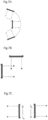
- Figures 7A to C is a view for illustrating such an arrangement relation of pairs of metal electrodes, seen from above, and the arrows shown are the directions of magnetic fields formed by energization of silicon cores.
- a rectangular plane formed by 2 pillar sections of U-shaped silicon cores 12 and a beam section linking these pillar sections to each other is arranged so as not to be even partially opposed to another rectangular plane of the U-shaped silicon cores 12 adjacently arranged.
- a rectangular plane formed by 2 pillar sections of U-shaped silicon cores 12 and a beam section linking these pillar sections to each other is arranged orthogonally to another rectangular plane of the U-shaped silicon cores 12 adjacently arranged.
- a rectangular plane formed by 2 pillar sections of U-shaped silicon cores 12 and a beam section linking these pillar sections to each other is arranged parallel to another rectangular plane of the U-shaped silicon cores 12 adjacently arranged, and to these silicon cores 12, current (i a , i b ) is applied that is phase-adjusted so that the direction of a magnetic field formed by each of the silicon cores 12 is opposite to each other.
- silicon cores are arranged on concentric circles centering at the center of the base plate.
- Figures 8A to C illustrate such an arrangement relation of pairs of metal electrodes, and dash lines shown are concentric circles centering at the center of the base plate.
- silicon cores 12 are arranged in the chamber, then, for example, 8 pairs of silicon cores 12 are preferably arranged on 2 concentric circles having different diameters, 4 pairs by 4 pairs.
- the above rectangular plane of silicon cores 12 arranged on an inner concentric circle and another rectangular plane of nearby silicon cores 12 arranged on an outer concentric circle are arranged so as not to be even partially opposed to each other.
- the above rectangular plane of silicon cores 12 arranged on an inner concentric circle and another rectangular plane of nearby silicon cores 12 arranged on an outer concentric circle are opposed to each other, but similarly as shown in Figure 7C , to these silicon cores 12, current (i a , i b ) is applied that is phase-adjusted so that the direction of a magnetic field formed by each of the silicon cores 12 is opposite to each other.
- Figure 9 is a flowchart for illustrating an example of a polycrystalline silicon rod manufacturing process according to the present invention when the reacting furnace 100 having the configuration shown in Figure 1 is used.
- a chamber 1 is mounted closely on a base plate 5, and a nitrogen gas is supplied from a source gas supply nozzle 9 into the chamber 1 to replace inside air with nitrogen (S101). Air and nitrogen inside the chamber 1 are discharged through an exhaust gas outlet 8 to the outside of the chamber 1. After replaced with nitrogen in the chamber 1, a hydrogen gas, instead of the nitrogen gas, is supplied from the source gas supply nozzle 9 to create a hydrogen environment in the chamber 1 (S102).
- silicon cores 12 are initially heated (preliminary heating) (S103).
- a carbon heater 13 is used, but a heated hydrogen gas may be supplied into the chamber 1. Due to this initial heating, the temperature of the silicon cores 12 is raised to not less than 300°C, and electric resistance of the silicon cores 12 takes such a value that energization can be efficiently performed.
- a mixed gas of a trichlorosilane gas containing silane compounds i.e. the source gas with a hydrogen gas, i.e. a carrier gas is supplied into the chamber 1 at a relatively slow flow (flow rate), and polycrystalline silicon begins to be vapor-grown on the silicon cores 12 (S105).
- the initial heating of the silicon cores may be performed in a nitrogen environment, and in this case, nitrogen has to be replaced with hydrogen before the trichlorosilane gas is supplied.
- the silicon cores 12 are thin and have not a high, mechanical strength. Accordingly, in an early period of vapor growth reaction of polycrystalline silicon, an ejection pressure at which the supply gas is supplied into the chamber 1 easily causes a trouble, such as a collapse of the silicon cores 12.
- the supply gas flow (flow rate) in the early period of vapor growth reaction is preferably set to a relatively low level (S106).
- the bulk concentration of the source gas is preferably kept between not less than 15 mol % and not more than 40 mol % till the diameter of the polycrystalline silicon rods reaches at least 15 mm (preferably 20 mm).
- the supply gas flow (flow rate) is preferably raised to near the maximum value after there is not a risk of collapse of the silicon cores 12 (polycrystalline silicon rods 11), or the like (S107).
- a setting of the supply gas flow (flow rate) may be performed, for example, at the time when the diameter of the polycrystalline silicon rods 11 reaches 20 mm, but the value of 40 mm may be used as a target.
- the gas is preferably supplied so that the pressure inside the chamber 1 is between 0.3 MPa and 0.9 MPa, and a flow rate at the exhaust outlet of the source gas supply nozzle 9 is preferably not less than 150 m/sec.
- the surface temperature of the polycrystalline silicon rods 11 is preferably kept relatively high, i.e. not less than 1000°C, and for example, the temperature is controlled in the range of 1000°C and 1250°C.
- the source gas containing silane compounds in a high concentration may cause a risk of occurrence of a large quantity of silicon fine particles, and these fine particles may adhere to the surfaces of the polycrystalline silicon rods 11 to provide a cause of contamination, or the like.
- the bulk concentration of the source gas in the supply gas is preferably lowered till the diameter of the polycrystalline silicon rods 11 reaches 130 mm at the latest (S108).
- the bulk concentration of the source gas trichlorosilane
- the bulk concentration of trichlorosilane is set between not less than 20 mol % and not more than 40 mol %.
- silicon crystal has a property that the higher its temperature is, the lower electric resistance becomes.
- the temperature in the central portions of the polycrystalline silicon rods becomes higher than that near the surfaces due to the electric heating and cooling near the surfaces when the diameter of the polycrystalline silicon rods becomes not less than a constant value.
- the electric resistance in the central portions of the polycrystalline silicon rods is lower compared to the electric resistance on the side of the surfaces, and this tendency becomes remarkable as the diameter expands.
- a high-frequency current shows a skin effect, and if a conductor is energized, a current density near the surface becomes high, as described above. This skin effect becomes more remarkable as a frequency is high, and current tends to concentrate on a surface.
- a depth at which current flows is called a "skin depth", or a "current penetration depth”.
- Figure 10A and Figure 10B are a view for illustrating a state of a current distribution in a cross-section and a view for illustrating the relation between I X and I 0 of the current distribution (I X /I 0 ) when current having a frequency of 80 kHz is applied through a polycrystalline silicon rod having a diameter of 160 mm, respectively.
- applying a high-frequency current heats a polycrystalline silicon rod, thereby allowing a region near the surface to be preferentially heated, and thus, the region near the surface can be preferentially heated even if the radius of the polycrystalline silicon rod expands. Therefore, a temperature distribution inside polycrystalline silicon can be prevented from being expanded to the extent of damaging manufacturing.
- Applying a high-frequency current in such a manner is preferably performed for a polycrystalline silicon rod whose diameter reaches a predetermined value D 0 of not less than 80 mm.
- Figure 11 is a view showing the result of the study of frequencies suitable for a high-frequency current used in the present invention. Frequencies were studied from 2 kHz to 200 kHz. According to the result shown, if the frequency is 800 kHz and the surface temperature of the polycrystalline silicon rod is 1150°C, then the penetration depth ⁇ is merely about 4 mm, and even if the temperature is 900°C, and the penetration depth ⁇ is only about 7 mm. Also, if the frequency is 200 kHz and the surface temperature of the polycrystalline silicon rod is 1150°C, then the penetration depth ⁇ is a little less than 9 mm, and even if the temperature is 900°C, it is only 13.7 mm.
- polycrystalline silicon will partially melt particularly due to concentration of the current density in a bend section of U-shaped silicon cores, and manufacturing may be damaged.
- Figure 12A and Figure 12B are views for illustrating a condition in which the crack of the polycrystalline silicon rods occurred, as described above, and an area where the crack occurred is shown by dashed lines.
- Figure 13 is a view for illustrating a current distribution in a cross-section when current having a frequency of 80 kHz and 200 kHz is applied through a polycrystalline silicon rod having a diameter of 160 mm. Note that the current distribution (I X /I 0 ) is calculated in a manner as shown in Figure 10B .
- a high-frequency current having a frequency of not less than 200 kHz is not suitable for use to electrically heat in the present invention.
- the frequency of a high-frequency current is selected so that the skin depth at which the current flows through polycrystalline silicon rods can take a desired value of not less than 13.8 mm and not more than 80.0 mm.
- the penetration depth of the high-frequency current is dependent on the temperature of polycrystalline silicon rods, and to provide the penetration depth in the range above, in the case of 1200°C, the frequency of the current is required to be between 67.2 kHz and 2.0 kHz, in the case of 1 100°C, between 93.7 kHz and 2.8 kHz, in the case of 1000°C, between 137.8 kHz and 4.1 kHz, in the case of 950°C, between 171.1 kHz and 5.1 kHz, and in the case of 900°C, between 216.3 kHz and 6.4 kHz.
- the source gas may be supplied to the surfaces of polycrystalline silicon rods, but as the diameter of the polycrystalline silicon rods increases and the surface areas become wider, the source gas supply tends to be insufficient. Accordingly, after the diameter of polycrystalline silicon rods becomes not less than 130 mm, it is preferable to lower the surface temperature by little and little (S109). For example, when the diameter reaches about 160 mm, the surface temperature is lowered to the range of not less than 950°C and less than 1030°C and if the diameter is further increased, then the surface temperature in the final stage is preferably lowered to the range of 900 and 980°C.
- Such a high-frequency current capable of providing the suitable penetration depth may also be used from the initial heating stage of silicon cores prior to the beginning of deposition reaction of polycrystalline silicon rods.
- m silicon cores (m is an integer of 2 or greater) are arranged in the reactor vessel, polycrystalline silicon is deposited on them, and n series-connected polycrystalline silicon rods (n is an integer of 2 or greater and not more than m) whose diameter reaches the predetermined value D 0 of not less than 80 mm due to the deposition of polycrystalline silicon may be supplied with a high-frequency current, and before this condition, current having a commercial frequency (low-frequency current) may be used for electric heating.
- low-frequency current commercial frequency
- a power source for applying this high-frequency current may be one high-frequency power source supplying a single high-frequency current, or one variable-frequency, high-frequency power source.
- variable-frequency may be continuously variable or variable step-by-step between a plurality of levels.
- variable-frequency, high-frequency power source may offer, for example, the following advantage.
- To control the surface temperature of polycrystalline silicon rods suitably, it is necessary to increase the amount of energization of polycrystalline silicon rods in response to radial expanding of silicon rods due to progression of the deposition reaction.
- the power source to be used has a single frequency, then using a power source having a little higher frequency becomes capable of controlling the total amount of current and provides an economical benefit, but if a power source having a little higher frequency is used, it becomes more difficult to control the penetration depth (skin depth) ⁇ more suitably by changing a frequency corresponding to the diameter of polycrystalline silicon rods.
- a plurality of frequencies of not less than 2 kHz may be made ready to be selected, and first, electric heating may be performed using current having the high-frequency f 1 , and when it becomes necessary to increase the amount of energization in order to maintain the surface temperature, the amount of energization may be increased by switching the current to current having the high-frequency f 2 of a little lower than the previous frequency f 1 .
- Increasing the amount of energization using the current having a little lower high-frequency f 2 as described above can prevent the skin effect from operating too much strongly. Note that such a control of the amount of energization may be performed using current control or voltage control.
- the current having a little lower high-frequency f 2 is applied and it is desired to increase a heating value near the surface in order to maintain the surface temperature, then the current is switched to the current having a little higher high-frequency f 1 to improve the skin effect, while the amount of energization being kept constant, thereby allowing the heating value near the surfaces to be increased without increasing the amount of energization.
- Such a variable range of frequencies is preferably between 2 kHz and 400 kHz, and generally, the larger the number of frequencies continuous or capable of being selected is, the more preferable it is.
- polycrystalline silicon rods having a diameter of about 160 mm whose surface temperature is about 980°C is heated using current having a frequency of 100 kHz and it is desired to raise the surface temperature to about 1000°C by increasing the amount of energization, then the frequency of the current is switched to 80 kHz lower than 100 kHz, the amount of energization is gradually increased by 10A to 50A per step, and it is observed how the temperature goes up.
- the frequency of the current is raised to 100 kHz while maintaining the amount of energization
- the frequency is raised to 120 kHz while maintaining the amount of energization, and so on, then it is observed how the temperature goes up. Even if the operations described above are carried out and the surface temperature begins to go down, then the frequency is lowered to 80 kHz and the amount of energization is gradually increased by 10A to 50A. Controlling the amount of energization and the current frequency alternately in a manner as described above can prevent too strong skin effect from being caused, suppress occurrence of the temperature difference between in the central portions and on the side of polycrystalline silicon rods, and further suppress power consumption efficiently.
- Figure 14 is a flowchart for illustrating a process example for enlarging a diameter of polycrystalline silicon rods while changing the frequency of a high-frequency current involving such a change in amount of energization.
- S201 diameter enlargement is promoted
- the surface temperature of silicon rods begins to go down.
- resistivity is lowered corresponding to rise in temperature and the penetration depth ⁇ becomes shallow, accordingly the surface temperature may become too high, thus first, the frequency of the high-frequency current is lowered to increase the penetration depth ⁇ (S202) and the amount of current is increased (S203).
- the penetration depth ⁇ is preliminarily increased in such a manner and the amount of energization is increased safely, thereby raising the surface temperature and enlarging the diameter (S204). If the surface temperature of the silicon rods goes down due to the diameter enlargement (S205), the frequency of the high-frequency current, this time, is increased to decrease the penetration depth ⁇ (S206), and the surface temperature is raised (S207). After this, it is intended to expand the diameter of the silicon rods while controlling the surface temperature of the polycrystalline silicon rods suitably (S201).
- the aforementioned description relates to the growth process of polycrystalline silicon rods, and also it is advantageous to use a high-frequency current in a cooling process after the growth of polycrystalline silicon rods ends.
- a frequency of the high-frequency current applied in the cooling process is preferably between not less than 2 kHz and not more than 100 kHz.
- Energization in such a cooling process may end at the stage when the surface temperature of polycrystalline silicon rods becomes, for example, not more than 500°C.
- a rough target for time duration of applying the high-frequency current in the cooling process is preferably about 4 hours, although depending on the diameter or the like.
- the method includes the high-frequency current applying process for heating polycrystalline silicon rods by applying through the polycrystalline silicon rods the current having a frequency of not less than 2 kHz
- the high-frequency current applying process includes supplying n series-connected polycrystalline silicon rods (n is an integer of 2 or greater and not more than m) whose diameter reaches the predetermined value D 0 of not less than 80 mm due to the deposition of polycrystalline silicon, with the high-frequency current from one high-frequency power source supplying a single high-frequency current or from one variable-frequency, high-frequency power source, then the frequency of the high-frequency current is set so that the skin depth at which the high-frequency current flows through the n series-connected polycrystalline silicon rods is in the range of not less than 13.8 mm and not more than 80.0 mm.
- Silicon cores 12 made from highly-pure polycrystalline silicon were arranged in a chamber 1 of a reacting furnace 100. After the silicon cores 12 were initially heated to 370°C using a carbon heater 13, a low-frequency current of 50 Hz, i.e. a commercial frequency, having an applied voltage of 2000 V began to be applied through the silicon cores 12.
- Deposition reaction of polycrystalline silicon on the silicon cores 12 began with supplying a mixed gas of trichlorosilane used as a source gas with a hydrogen gas, i.e. a carrier gas under conditions in which a voltage of 1050 V was applied to the silicon cores 12 and the surface temperature was 1160°C.
- the deposition reaction continued under the condition of energization above till the diameter of the polycrystalline silicon reached 82 mm, subsequently the current was switched to a high-frequency current having a frequency of 80 kHz and it was applied, and the reaction continued till the diameter of the polycrystalline silicon rods reached 163 mm. Note that at the end of the reaction, that is, at the time when the diameter of the polycrystalline silicon rods reached 163 mm, supply power was 363 kW.
- cooling was carried out by gradually reducing the amount of energization while continuing to apply the high-frequency current having a frequency of 80 kHz till the surface temperature of the polycrystalline silicon rods lowered to 600°C, and subsequently the energization was stopped.
- the polycrystalline silicon rods 11 were left uncontrolled in the chamber 1 before the surface temperature of the polycrystalline silicon rods 11 became 45°C, and the polycrystalline silicon rods 11 were removed out.
- Silicon cores 12 made from highly-pure polycrystalline silicon were arranged in the chamber 1 of the reacting furnace 100. After the silicon cores 12 were initially heated to 340°C using the carbon heater 13, a low-frequency current of 50 Hz, i.e. a commercial frequency, having an applied voltage of 2000 V began to be applied through the silicon cores 12.
- Deposition reaction of polycrystalline silicon on the silicon cores 12 began with supplying a mixed gas of trichlorosilane used as a source gas with a hydrogen gas, i.e. a carrier gas under conditions in which a voltage of 1050 V was applied through the silicon cores 12 and the surface temperature was 1130°C.
- cooling was carried out by gradually reducing the amount of energization while continuing to apply the low-frequency current having a frequency of 50 Hz till the surface temperature of the polycrystalline silicon rods lowered to 600°C, and subsequently the energization was stopped.
- Silicon cores 12 made from highly-pure polycrystalline silicon were arranged in the chamber 1 of the reacting furnace 100. After the silicon cores 12 were initially heated to 355°C using the carbon heater 13, a low-frequency current of 50 Hz, i.e. a commercial frequency, having an applied voltage of 2000 V began to be applied through the silicon cores 12.
- Deposition reaction of polycrystalline silicon on the silicon cores 12 began with supplying a mixed gas of trichlorosilane used as a source gas with a hydrogen gas, i.e. a carrier gas, under conditions in which a voltage of 1010 V was applied to the silicon cores 12 and the surface temperature was 1100°C.
- the deposition reaction continued under the condition of energization above till the diameter of the polycrystalline silicon reached 80 mm, also subsequently, the low-frequency current having a frequency of 50 Hz continued to be applied, thus expanding the diameter.
- the polycrystalline silicon rods reached 159 mm, they collapsed. Note that when the polycrystalline silicon rods reached 159 mm, supply power was 448 kW.
- the polycrystalline silicon rod manufacturing method according to the present invention may include a configuration described below.
- a source gas containing silane compounds is supplied into a reacting furnace, and polycrystalline silicon is deposited on the silicon cores electrically heated using the CVD method to manufacture polycrystalline silicon rods
- a high-frequency current applying process is provided in which the polycrystalline silicon rods are heated by applying through the polycrystalline silicon rods a current having a frequency of not less than 2 kHz.
- This high-frequency current applying process includes a process in which n polycrystalline silicon rods (n is an integer of 2 or greater and not more than m) whose diameter reaches a predetermined value D 0 of not less than 80 mm due to the deposition of polycrystalline silicon are connected to each other in series, and the n series-connected polycrystalline silicon rods are supplied with a high-frequency current from one high-frequency power source supplying a single high-frequency current.
- the frequency of the high-frequency current is set so that the skin depth at which the high-frequency current flows through the n series-connected polycrystalline silicon rods takes a desired value in the range of not less than 13.8 mm and not more than 80.0 mm.
- the polycrystalline silicon rod manufacturing method according to the present invention may include a configuration described below.
- the high-frequency current applying process described above includes a process in which n polycrystalline silicon rods (n is an integer of 2 or greater and not more than m) whose diameter reaches a predetermined value D 0 of not less than 80 mm due to the deposition of polycrystalline silicon are connected to each other in series, and the n series-connected polycrystalline silicon rods are supplied with a high-frequency current from one variable-frequency, high-frequency power source, and the frequency of the high-frequency current is changed in response to variation in surface temperature of the polycrystalline silicon rods to the extent that the skin depth at which the high-frequency current flows through the n series-connected polycrystalline silicon rods takes a desired value in the range of not less than 13.8 mm and not more than 80.0 mm.
- the silicon cores may begin to be heated by applying through the silicon cores the low-frequency current or the high-frequency current, and after the surfaces of the silicon cores become a desired temperature, polycrystalline silicon may begin to be deposited.
- m silicon cores may be connected to each other in parallel, and the silicon cores may begin to be heated by supplying the parallel-connected silicon cores with current from one low-frequency power source supplying a low-frequency current.
- m silicon cores may be connected to each other in series in order from a first one to an m-th, and the silicon cores may begin to be heated by supplying the series-connected silicon cores with current from one low-frequency power source or from one high-frequency power source.
- m polycrystalline silicon rods may be connected to each other in parallel, and the polycrystalline silicon rods may be heated by supplying the parallel-connected polycrystalline silicon rods with current from one low-frequency power source supplying a low-frequency current.
- M silicon cores (M is an integer of 2 or greater) may be further arranged in the reactor vessel, and polycrystalline silicon may be deposited on the M silicon cores in a similar manner as that of the deposition of polycrystalline silicon on the m silicon cores, using a high-frequency power source provided separately from the one high-frequency power source and supplying a single high-frequency current having a frequency of not less than 2 kHz, or one variable-frequency, high-frequency power source supplying current having a frequency of not less than 2 kHz.
- a gas containing trichlorosilane is selected as a source gas, and the surface temperature of polycrystalline silicon rods is controlled in the range of not less than 900°C and not more than 1250°C to deposit polycrystalline silicon.
- the present invention provides technologies for manufacturing polycrystalline silicon rods having a large diameter with a high efficiency while using trichlorosilane as a raw material and preventing a collapse that easily occurs when the polycrystalline silicon rods having a large diameter are manufactured.
Landscapes
- Chemical & Material Sciences (AREA)
- Organic Chemistry (AREA)
- Engineering & Computer Science (AREA)
- Metallurgy (AREA)
- Materials Engineering (AREA)
- Mechanical Engineering (AREA)
- Chemical Kinetics & Catalysis (AREA)
- General Chemical & Material Sciences (AREA)
- Inorganic Chemistry (AREA)
- Physics & Mathematics (AREA)
- Plasma & Fusion (AREA)
- Silicon Compounds (AREA)
- Crystals, And After-Treatments Of Crystals (AREA)
Claims (2)
- Méthode de fabrication de bâtonnets de silicium polycristallin, dans laquelle m coeurs de silicium, m étant un nombre entier valant 2 ou plus, sont disposés dans une cuve de réacteur, un gaz source contenant du trichlorosilane est amené dans la cuve de réacteur, et du silicium polycristallin est déposé sur les coeurs de silicium chauffés électriquement par une technique CVD, afin d'obtenir des bâtonnets de silicium polycristallin ayant un diamètre non inférieur à 160 mm,la méthode comprenant un procédé d'application de courant à haute fréquence pour chauffer les bâtonnets de silicium polycristallin en appliquant, à travers les bâtonnets de silicium polycristallin, un courant ayant une fréquence non inférieure à 2 kHz,dans lequel le procédé d'application de courant à haute fréquence consiste à fournir un courant à haute fréquence à partir d'une source d'énergie à haute fréquence unique fournissant un seul courant à haute fréquence à n bâtonnets de silicium polycristallin, n étant un nombre entier valant de 2 ou plus et pas plus de m, connectés les uns aux autres en série et dont le diamètre atteint une valeur prédéterminée D0 non inférieure à 80 mm en raison du dépôt de silicium polycristallin, etune fréquence du courant à haute fréquence est réglée de telle sorte qu'une profondeur de pénétration à laquelle le courant à haute fréquence circule à travers les n bâtonnets de silicium polycristallin connectés en série prenne une valeur souhaitée dans une plage non inférieure à 13,8 mm et non supérieure à 80,0 mm,où une température de surface des bâtonnets de silicium polycristallin est contrôlée dans une plage non inférieure à 900°C et non supérieure à 1250°C pour déposer du silicium polycristallin ;
la méthode comprenant en outre :un procédé pour chauffer les coeurs de silicium en appliquant un courant à travers les coeurs de silicium avant le procédé d'application de courant à haute fréquence, etun procédé pour commencer un dépôt de silicium polycristallin sur les surfaces des coeurs de silicium une fois que les surfaces des coeurs de silicium ont atteint une température souhaitée ; etoù les m coeurs de silicium sont connectés les uns aux autres en parallèle avant le procédé de chauffage des coeurs de silicium,puis le courant provenant d'une source d'énergie à basse fréquence unique fournit un courant à basse fréquence aux m coeurs de silicium, etlorsque le diamètre des m bâtonnets de silicium polycristallin atteint la valeur prédéterminée D0, les m bâtonnets de silicium polycristallin sont commutés pour être connectés les uns aux autres en série, et le procédé d'application de courant à haute fréquence est mis en oeuvre par la fourniture du courant à haute fréquence à partir de la source d'énergie à haute fréquence unique. - Méthode de fabrication de bâtonnets de silicium polycristallin selon la revendication 1, dans laquelleM coeurs de silicium, M étant un nombre entier valant 2 ou plus, sont en outre disposés dans la cuve de réacteur, etdu silicium polycristallin est déposé sur les M coeurs de silicium d'une manière similaire à celle du dépôt de silicium polycristallin sur les m coeurs de silicium, en utilisant une source d'énergie à haute fréquence fournie séparément de la source d'énergie à haute fréquence unique et en fournissant un seul courant à haute fréquence ayant une fréquence non inférieure à 2 kHz.
Applications Claiming Priority (2)
| Application Number | Priority Date | Filing Date | Title |
|---|---|---|---|
| JP2012037150A JP5792657B2 (ja) | 2012-02-23 | 2012-02-23 | 多結晶シリコン棒の製造方法 |
| PCT/JP2013/000892 WO2013125207A1 (fr) | 2012-02-23 | 2013-02-19 | Procédé de fabrication d'une tige de silicium polycristallin |
Publications (3)
| Publication Number | Publication Date |
|---|---|
| EP2818450A1 EP2818450A1 (fr) | 2014-12-31 |
| EP2818450A4 EP2818450A4 (fr) | 2015-12-02 |
| EP2818450B1 true EP2818450B1 (fr) | 2023-11-08 |
Family
ID=49005403
Family Applications (1)
| Application Number | Title | Priority Date | Filing Date |
|---|---|---|---|
| EP13751736.3A Active EP2818450B1 (fr) | 2012-02-23 | 2013-02-19 | Procédé de fabrication d'une tige de silicium polycristallin |
Country Status (7)
| Country | Link |
|---|---|
| US (1) | US20150017349A1 (fr) |
| EP (1) | EP2818450B1 (fr) |
| JP (1) | JP5792657B2 (fr) |
| KR (1) | KR20140125354A (fr) |
| CN (2) | CN106976884B (fr) |
| MY (1) | MY168538A (fr) |
| WO (1) | WO2013125207A1 (fr) |
Families Citing this family (10)
| Publication number | Priority date | Publication date | Assignee | Title |
|---|---|---|---|---|
| JP6181620B2 (ja) * | 2014-09-04 | 2017-08-16 | 信越化学工業株式会社 | 多結晶シリコン製造用反応炉、多結晶シリコン製造装置、多結晶シリコンの製造方法、及び、多結晶シリコン棒または多結晶シリコン塊 |
| CN106115712B (zh) * | 2016-06-28 | 2019-04-05 | 重庆大全泰来电气有限公司 | 一种多晶硅还原炉电源系统 |
| JP2018123033A (ja) * | 2017-02-02 | 2018-08-09 | 信越化学工業株式会社 | 多結晶シリコン棒の製造方法および多結晶シリコン棒 |
| JP6969917B2 (ja) * | 2017-07-12 | 2021-11-24 | 信越化学工業株式会社 | 多結晶シリコン棒および多結晶シリコン棒の製造方法 |
| CN110182813B (zh) * | 2019-06-12 | 2021-01-12 | 厦门佰事兴新材料科技有限公司 | 还原炉电极的维护方法 |
| JP7191780B2 (ja) | 2019-06-17 | 2022-12-19 | 信越化学工業株式会社 | 多結晶シリコンロッドの製造方法 |
| JP6805398B1 (ja) * | 2019-07-12 | 2020-12-23 | 株式会社トクヤマ | 多結晶シリコンの製造方法 |
| CN110683547B (zh) * | 2019-11-18 | 2023-12-26 | 新疆东方希望新能源有限公司 | 一种72对棒还原炉高压击穿系统及其方法 |
| CN114545865B (zh) * | 2020-11-25 | 2024-01-30 | 新特能源股份有限公司 | 一种多晶硅生长控制方法 |
| CN114212794B (zh) * | 2021-12-30 | 2023-03-28 | 新疆大全新能源股份有限公司 | 制备电子级方硅芯的原生多晶硅棒的生产方法 |
Family Cites Families (8)
| Publication number | Priority date | Publication date | Assignee | Title |
|---|---|---|---|---|
| DE2727305A1 (de) * | 1977-06-16 | 1979-01-04 | Siemens Ag | Verfahren zum abscheiden von feinkristallinem silicium aus der gasphase an der oberflaeche eines erhitzten traegerkoerpers |
| DE2831816A1 (de) | 1978-07-19 | 1980-01-31 | Siemens Ag | Verfahren zum abscheiden von silicium in feinkristalliner form |
| JPS6374909A (ja) | 1986-09-19 | 1988-04-05 | Shin Etsu Handotai Co Ltd | 大直径多結晶シリコン棒の製造方法 |
| JPH01305810A (ja) * | 1988-06-02 | 1989-12-11 | Osaka Titanium Co Ltd | 多結晶シリコンの通電加熱方法 |
| US6221155B1 (en) * | 1997-12-15 | 2001-04-24 | Advanced Silicon Materials, Llc | Chemical vapor deposition system for polycrystalline silicon rod production |
| JP3621311B2 (ja) * | 1999-11-15 | 2005-02-16 | 住友チタニウム株式会社 | 多結晶シリコン製造プロセスにおけるシリコン直径及び温度の推定方法並びにこれを用いた操業管理方法 |
| US7521341B2 (en) * | 2005-11-09 | 2009-04-21 | Industrial Technology Research Institute | Method of direct deposition of polycrystalline silicon |
| KR100768147B1 (ko) * | 2006-05-11 | 2007-10-18 | 한국화학연구원 | 혼합된 코어수단을 이용한 다결정 실리콘 봉의 제조방법과그 제조장치 |
-
2012
- 2012-02-23 JP JP2012037150A patent/JP5792657B2/ja active Active
-
2013
- 2013-02-19 MY MYPI2014702225A patent/MY168538A/en unknown
- 2013-02-19 EP EP13751736.3A patent/EP2818450B1/fr active Active
- 2013-02-19 US US14/380,249 patent/US20150017349A1/en not_active Abandoned
- 2013-02-19 KR KR1020147019662A patent/KR20140125354A/ko not_active Application Discontinuation
- 2013-02-19 CN CN201710051831.5A patent/CN106976884B/zh active Active
- 2013-02-19 CN CN201380006296.1A patent/CN104066679A/zh active Pending
- 2013-02-19 WO PCT/JP2013/000892 patent/WO2013125207A1/fr active Application Filing
Also Published As
| Publication number | Publication date |
|---|---|
| US20150017349A1 (en) | 2015-01-15 |
| KR20140125354A (ko) | 2014-10-28 |
| EP2818450A1 (fr) | 2014-12-31 |
| JP2013170117A (ja) | 2013-09-02 |
| EP2818450A4 (fr) | 2015-12-02 |
| CN106976884B (zh) | 2019-09-27 |
| MY168538A (en) | 2018-11-12 |
| CN106976884A (zh) | 2017-07-25 |
| JP5792657B2 (ja) | 2015-10-14 |
| CN104066679A (zh) | 2014-09-24 |
| WO2013125207A1 (fr) | 2013-08-29 |
Similar Documents
| Publication | Publication Date | Title |
|---|---|---|
| EP2818450B1 (fr) | Procédé de fabrication d'une tige de silicium polycristallin | |
| US9394606B2 (en) | Production method for polycrystalline silicon, and reactor for polycrystalline silicon production | |
| CA2986250C (fr) | Synthese de nanotubes de nitrure de bore par induction directe | |
| EP2818449B1 (fr) | Procédé de fabrication d'une tige de silicium polycristallin | |
| US10870581B2 (en) | Reaction furnace for producing polycrystalline silicon, apparatus for producing polycrystalline silicon, method for producing polycrystalline silicon, and polycrystalline silicon rod or polycrystalline silicon ingot | |
| CN103510156A (zh) | 多晶硅棒 | |
| JP5539292B2 (ja) | 多結晶シリコンの製造方法 | |
| JP5917359B2 (ja) | 多結晶シリコン製造用原料ガスの供給方法および多結晶シリコン | |
| JP2013071856A (ja) | 多結晶シリコン製造装置および多結晶シリコンの製造方法 | |
| JP2020203808A (ja) | 多結晶シリコンロッドの製造方法 |
Legal Events
| Date | Code | Title | Description |
|---|---|---|---|
| PUAI | Public reference made under article 153(3) epc to a published international application that has entered the european phase |
Free format text: ORIGINAL CODE: 0009012 |
|
| STAA | Information on the status of an ep patent application or granted ep patent |
Free format text: STATUS: REQUEST FOR EXAMINATION WAS MADE |
|
| 17P | Request for examination filed |
Effective date: 20140815 |
|
| AK | Designated contracting states |
Kind code of ref document: A1 Designated state(s): AL AT BE BG CH CY CZ DE DK EE ES FI FR GB GR HR HU IE IS IT LI LT LU LV MC MK MT NL NO PL PT RO RS SE SI SK SM TR |
|
| AX | Request for extension of the european patent |
Extension state: BA ME |
|
| DAX | Request for extension of the european patent (deleted) | ||
| RA4 | Supplementary search report drawn up and despatched (corrected) |
Effective date: 20151030 |
|
| RIC1 | Information provided on ipc code assigned before grant |
Ipc: C23C 16/24 20060101ALI20151026BHEP Ipc: C01B 33/035 20060101AFI20151026BHEP Ipc: C23C 16/46 20060101ALI20151026BHEP |
|
| STAA | Information on the status of an ep patent application or granted ep patent |
Free format text: STATUS: EXAMINATION IS IN PROGRESS |
|
| 17Q | First examination report despatched |
Effective date: 20210507 |
|
| STAA | Information on the status of an ep patent application or granted ep patent |
Free format text: STATUS: EXAMINATION IS IN PROGRESS |
|
| GRAP | Despatch of communication of intention to grant a patent |
Free format text: ORIGINAL CODE: EPIDOSNIGR1 |
|
| STAA | Information on the status of an ep patent application or granted ep patent |
Free format text: STATUS: GRANT OF PATENT IS INTENDED |
|
| INTG | Intention to grant announced |
Effective date: 20230605 |
|
| GRAS | Grant fee paid |
Free format text: ORIGINAL CODE: EPIDOSNIGR3 |
|
| GRAA | (expected) grant |
Free format text: ORIGINAL CODE: 0009210 |
|
| STAA | Information on the status of an ep patent application or granted ep patent |
Free format text: STATUS: THE PATENT HAS BEEN GRANTED |
|
| AK | Designated contracting states |
Kind code of ref document: B1 Designated state(s): AL AT BE BG CH CY CZ DE DK EE ES FI FR GB GR HR HU IE IS IT LI LT LU LV MC MK MT NL NO PL PT RO RS SE SI SK SM TR |
|
| REG | Reference to a national code |
Ref country code: GB Ref legal event code: FG4D |
|
| REG | Reference to a national code |
Ref country code: CH Ref legal event code: EP |
|
| REG | Reference to a national code |
Ref country code: DE Ref legal event code: R096 Ref document number: 602013084899 Country of ref document: DE |
|
| REG | Reference to a national code |
Ref country code: IE Ref legal event code: FG4D |
|
| REG | Reference to a national code |
Ref country code: LT Ref legal event code: MG9D |
|
| REG | Reference to a national code |
Ref country code: NL Ref legal event code: MP Effective date: 20231108 |
|
| PG25 | Lapsed in a contracting state [announced via postgrant information from national office to epo] |
Ref country code: GR Free format text: LAPSE BECAUSE OF FAILURE TO SUBMIT A TRANSLATION OF THE DESCRIPTION OR TO PAY THE FEE WITHIN THE PRESCRIBED TIME-LIMIT Effective date: 20240209 |
|
| PG25 | Lapsed in a contracting state [announced via postgrant information from national office to epo] |
Ref country code: IS Free format text: LAPSE BECAUSE OF FAILURE TO SUBMIT A TRANSLATION OF THE DESCRIPTION OR TO PAY THE FEE WITHIN THE PRESCRIBED TIME-LIMIT Effective date: 20240308 |
|
| PG25 | Lapsed in a contracting state [announced via postgrant information from national office to epo] |
Ref country code: LT Free format text: LAPSE BECAUSE OF FAILURE TO SUBMIT A TRANSLATION OF THE DESCRIPTION OR TO PAY THE FEE WITHIN THE PRESCRIBED TIME-LIMIT Effective date: 20231108 |
|
| REG | Reference to a national code |
Ref country code: AT Ref legal event code: MK05 Ref document number: 1629481 Country of ref document: AT Kind code of ref document: T Effective date: 20231108 |
|
| PG25 | Lapsed in a contracting state [announced via postgrant information from national office to epo] |
Ref country code: NL Free format text: LAPSE BECAUSE OF FAILURE TO SUBMIT A TRANSLATION OF THE DESCRIPTION OR TO PAY THE FEE WITHIN THE PRESCRIBED TIME-LIMIT Effective date: 20231108 |
|
| PG25 | Lapsed in a contracting state [announced via postgrant information from national office to epo] |
Ref country code: AT Free format text: LAPSE BECAUSE OF FAILURE TO SUBMIT A TRANSLATION OF THE DESCRIPTION OR TO PAY THE FEE WITHIN THE PRESCRIBED TIME-LIMIT Effective date: 20231108 |
|
| PG25 | Lapsed in a contracting state [announced via postgrant information from national office to epo] |
Ref country code: ES Free format text: LAPSE BECAUSE OF FAILURE TO SUBMIT A TRANSLATION OF THE DESCRIPTION OR TO PAY THE FEE WITHIN THE PRESCRIBED TIME-LIMIT Effective date: 20231108 |
|
| PG25 | Lapsed in a contracting state [announced via postgrant information from national office to epo] |
Ref country code: NL Free format text: LAPSE BECAUSE OF FAILURE TO SUBMIT A TRANSLATION OF THE DESCRIPTION OR TO PAY THE FEE WITHIN THE PRESCRIBED TIME-LIMIT Effective date: 20231108 Ref country code: LT Free format text: LAPSE BECAUSE OF FAILURE TO SUBMIT A TRANSLATION OF THE DESCRIPTION OR TO PAY THE FEE WITHIN THE PRESCRIBED TIME-LIMIT Effective date: 20231108 Ref country code: IS Free format text: LAPSE BECAUSE OF FAILURE TO SUBMIT A TRANSLATION OF THE DESCRIPTION OR TO PAY THE FEE WITHIN THE PRESCRIBED TIME-LIMIT Effective date: 20240308 Ref country code: GR Free format text: LAPSE BECAUSE OF FAILURE TO SUBMIT A TRANSLATION OF THE DESCRIPTION OR TO PAY THE FEE WITHIN THE PRESCRIBED TIME-LIMIT Effective date: 20240209 Ref country code: ES Free format text: LAPSE BECAUSE OF FAILURE TO SUBMIT A TRANSLATION OF THE DESCRIPTION OR TO PAY THE FEE WITHIN THE PRESCRIBED TIME-LIMIT Effective date: 20231108 Ref country code: BG Free format text: LAPSE BECAUSE OF FAILURE TO SUBMIT A TRANSLATION OF THE DESCRIPTION OR TO PAY THE FEE WITHIN THE PRESCRIBED TIME-LIMIT Effective date: 20240208 Ref country code: AT Free format text: LAPSE BECAUSE OF FAILURE TO SUBMIT A TRANSLATION OF THE DESCRIPTION OR TO PAY THE FEE WITHIN THE PRESCRIBED TIME-LIMIT Effective date: 20231108 Ref country code: PT Free format text: LAPSE BECAUSE OF FAILURE TO SUBMIT A TRANSLATION OF THE DESCRIPTION OR TO PAY THE FEE WITHIN THE PRESCRIBED TIME-LIMIT Effective date: 20240308 |
|
| PGFP | Annual fee paid to national office [announced via postgrant information from national office to epo] |
Ref country code: DE Payment date: 20240116 Year of fee payment: 12 |
|
| PG25 | Lapsed in a contracting state [announced via postgrant information from national office to epo] |
Ref country code: SE Free format text: LAPSE BECAUSE OF FAILURE TO SUBMIT A TRANSLATION OF THE DESCRIPTION OR TO PAY THE FEE WITHIN THE PRESCRIBED TIME-LIMIT Effective date: 20231108 Ref country code: RS Free format text: LAPSE BECAUSE OF FAILURE TO SUBMIT A TRANSLATION OF THE DESCRIPTION OR TO PAY THE FEE WITHIN THE PRESCRIBED TIME-LIMIT Effective date: 20231108 Ref country code: PL Free format text: LAPSE BECAUSE OF FAILURE TO SUBMIT A TRANSLATION OF THE DESCRIPTION OR TO PAY THE FEE WITHIN THE PRESCRIBED TIME-LIMIT Effective date: 20231108 Ref country code: NO Free format text: LAPSE BECAUSE OF FAILURE TO SUBMIT A TRANSLATION OF THE DESCRIPTION OR TO PAY THE FEE WITHIN THE PRESCRIBED TIME-LIMIT Effective date: 20240208 Ref country code: LV Free format text: LAPSE BECAUSE OF FAILURE TO SUBMIT A TRANSLATION OF THE DESCRIPTION OR TO PAY THE FEE WITHIN THE PRESCRIBED TIME-LIMIT Effective date: 20231108 Ref country code: HR Free format text: LAPSE BECAUSE OF FAILURE TO SUBMIT A TRANSLATION OF THE DESCRIPTION OR TO PAY THE FEE WITHIN THE PRESCRIBED TIME-LIMIT Effective date: 20231108 |
|
| PG25 | Lapsed in a contracting state [announced via postgrant information from national office to epo] |
Ref country code: DK Free format text: LAPSE BECAUSE OF FAILURE TO SUBMIT A TRANSLATION OF THE DESCRIPTION OR TO PAY THE FEE WITHIN THE PRESCRIBED TIME-LIMIT Effective date: 20231108 |
|
| PG25 | Lapsed in a contracting state [announced via postgrant information from national office to epo] |
Ref country code: CZ Free format text: LAPSE BECAUSE OF FAILURE TO SUBMIT A TRANSLATION OF THE DESCRIPTION OR TO PAY THE FEE WITHIN THE PRESCRIBED TIME-LIMIT Effective date: 20231108 |
|
| PG25 | Lapsed in a contracting state [announced via postgrant information from national office to epo] |
Ref country code: SK Free format text: LAPSE BECAUSE OF FAILURE TO SUBMIT A TRANSLATION OF THE DESCRIPTION OR TO PAY THE FEE WITHIN THE PRESCRIBED TIME-LIMIT Effective date: 20231108 |
|
| PG25 | Lapsed in a contracting state [announced via postgrant information from national office to epo] |
Ref country code: SM Free format text: LAPSE BECAUSE OF FAILURE TO SUBMIT A TRANSLATION OF THE DESCRIPTION OR TO PAY THE FEE WITHIN THE PRESCRIBED TIME-LIMIT Effective date: 20231108 Ref country code: SK Free format text: LAPSE BECAUSE OF FAILURE TO SUBMIT A TRANSLATION OF THE DESCRIPTION OR TO PAY THE FEE WITHIN THE PRESCRIBED TIME-LIMIT Effective date: 20231108 Ref country code: RO Free format text: LAPSE BECAUSE OF FAILURE TO SUBMIT A TRANSLATION OF THE DESCRIPTION OR TO PAY THE FEE WITHIN THE PRESCRIBED TIME-LIMIT Effective date: 20231108 Ref country code: IT Free format text: LAPSE BECAUSE OF FAILURE TO SUBMIT A TRANSLATION OF THE DESCRIPTION OR TO PAY THE FEE WITHIN THE PRESCRIBED TIME-LIMIT Effective date: 20231108 Ref country code: EE Free format text: LAPSE BECAUSE OF FAILURE TO SUBMIT A TRANSLATION OF THE DESCRIPTION OR TO PAY THE FEE WITHIN THE PRESCRIBED TIME-LIMIT Effective date: 20231108 Ref country code: DK Free format text: LAPSE BECAUSE OF FAILURE TO SUBMIT A TRANSLATION OF THE DESCRIPTION OR TO PAY THE FEE WITHIN THE PRESCRIBED TIME-LIMIT Effective date: 20231108 Ref country code: CZ Free format text: LAPSE BECAUSE OF FAILURE TO SUBMIT A TRANSLATION OF THE DESCRIPTION OR TO PAY THE FEE WITHIN THE PRESCRIBED TIME-LIMIT Effective date: 20231108 |
|
| REG | Reference to a national code |
Ref country code: DE Ref legal event code: R097 Ref document number: 602013084899 Country of ref document: DE |
|
| PLBE | No opposition filed within time limit |
Free format text: ORIGINAL CODE: 0009261 |
|
| STAA | Information on the status of an ep patent application or granted ep patent |
Free format text: STATUS: NO OPPOSITION FILED WITHIN TIME LIMIT |
|
| PG25 | Lapsed in a contracting state [announced via postgrant information from national office to epo] |
Ref country code: MC Free format text: LAPSE BECAUSE OF FAILURE TO SUBMIT A TRANSLATION OF THE DESCRIPTION OR TO PAY THE FEE WITHIN THE PRESCRIBED TIME-LIMIT Effective date: 20231108 |
|
| REG | Reference to a national code |
Ref country code: CH Ref legal event code: PL |
|
| PG25 | Lapsed in a contracting state [announced via postgrant information from national office to epo] |
Ref country code: LU Free format text: LAPSE BECAUSE OF NON-PAYMENT OF DUE FEES Effective date: 20240219 |
|
| 26N | No opposition filed |
Effective date: 20240809 |