EP2815429B1 - Multi-chip module comprising a compressible structure and method for maintaining alignment in a multi-chip module using a compressible structure - Google Patents
Multi-chip module comprising a compressible structure and method for maintaining alignment in a multi-chip module using a compressible structure Download PDFInfo
- Publication number
- EP2815429B1 EP2815429B1 EP13749252.6A EP13749252A EP2815429B1 EP 2815429 B1 EP2815429 B1 EP 2815429B1 EP 13749252 A EP13749252 A EP 13749252A EP 2815429 B1 EP2815429 B1 EP 2815429B1
- Authority
- EP
- European Patent Office
- Prior art keywords
- mcm
- chip
- compressible structure
- bridge chip
- island
- Prior art date
- Legal status (The legal status is an assumption and is not a legal conclusion. Google has not performed a legal analysis and makes no representation as to the accuracy of the status listed.)
- Active
Links
Images


Classifications
-
- H—ELECTRICITY
- H01—ELECTRIC ELEMENTS
- H01L—SEMICONDUCTOR DEVICES NOT COVERED BY CLASS H10
- H01L25/00—Assemblies consisting of a plurality of semiconductor or other solid state devices
- H01L25/03—Assemblies consisting of a plurality of semiconductor or other solid state devices all the devices being of a type provided for in a single subclass of subclasses H10B, H10D, H10F, H10H, H10K or H10N, e.g. assemblies of rectifier diodes
- H01L25/04—Assemblies consisting of a plurality of semiconductor or other solid state devices all the devices being of a type provided for in a single subclass of subclasses H10B, H10D, H10F, H10H, H10K or H10N, e.g. assemblies of rectifier diodes the devices not having separate containers
- H01L25/065—Assemblies consisting of a plurality of semiconductor or other solid state devices all the devices being of a type provided for in a single subclass of subclasses H10B, H10D, H10F, H10H, H10K or H10N, e.g. assemblies of rectifier diodes the devices not having separate containers the devices being of a type provided for in group H10D89/00
- H01L25/0652—Assemblies consisting of a plurality of semiconductor or other solid state devices all the devices being of a type provided for in a single subclass of subclasses H10B, H10D, H10F, H10H, H10K or H10N, e.g. assemblies of rectifier diodes the devices not having separate containers the devices being of a type provided for in group H10D89/00 the devices being arranged next and on each other, i.e. mixed assemblies
-
- H—ELECTRICITY
- H01—ELECTRIC ELEMENTS
- H01L—SEMICONDUCTOR DEVICES NOT COVERED BY CLASS H10
- H01L23/00—Details of semiconductor or other solid state devices
- H01L23/48—Arrangements for conducting electric current to or from the solid state body in operation, e.g. leads, terminal arrangements ; Selection of materials therefor
-
- H—ELECTRICITY
- H01—ELECTRIC ELEMENTS
- H01L—SEMICONDUCTOR DEVICES NOT COVERED BY CLASS H10
- H01L24/00—Arrangements for connecting or disconnecting semiconductor or solid-state bodies; Methods or apparatus related thereto
- H01L24/71—Means for bonding not being attached to, or not being formed on, the surface to be connected
- H01L24/72—Detachable connecting means consisting of mechanical auxiliary parts connecting the device, e.g. pressure contacts using springs or clips
-
- H—ELECTRICITY
- H01—ELECTRIC ELEMENTS
- H01L—SEMICONDUCTOR DEVICES NOT COVERED BY CLASS H10
- H01L24/00—Arrangements for connecting or disconnecting semiconductor or solid-state bodies; Methods or apparatus related thereto
- H01L24/73—Means for bonding being of different types provided for in two or more of groups H01L24/10, H01L24/18, H01L24/26, H01L24/34, H01L24/42, H01L24/50, H01L24/63, H01L24/71
-
- H—ELECTRICITY
- H01—ELECTRIC ELEMENTS
- H01L—SEMICONDUCTOR DEVICES NOT COVERED BY CLASS H10
- H01L24/00—Arrangements for connecting or disconnecting semiconductor or solid-state bodies; Methods or apparatus related thereto
- H01L24/90—Methods for connecting semiconductor or solid state bodies using means for bonding not being attached to, or not being formed on, the body surface to be connected, e.g. pressure contacts using springs or clips
-
- H—ELECTRICITY
- H01—ELECTRIC ELEMENTS
- H01L—SEMICONDUCTOR DEVICES NOT COVERED BY CLASS H10
- H01L24/00—Arrangements for connecting or disconnecting semiconductor or solid-state bodies; Methods or apparatus related thereto
- H01L24/91—Methods for connecting semiconductor or solid state bodies including different methods provided for in two or more of groups H01L24/80 - H01L24/90
-
- H—ELECTRICITY
- H01—ELECTRIC ELEMENTS
- H01L—SEMICONDUCTOR DEVICES NOT COVERED BY CLASS H10
- H01L25/00—Assemblies consisting of a plurality of semiconductor or other solid state devices
- H01L25/50—Multistep manufacturing processes of assemblies consisting of devices, the devices being individual devices of subclass H10D or integrated devices of class H10
-
- H—ELECTRICITY
- H01—ELECTRIC ELEMENTS
- H01L—SEMICONDUCTOR DEVICES NOT COVERED BY CLASS H10
- H01L2224/00—Indexing scheme for arrangements for connecting or disconnecting semiconductor or solid-state bodies and methods related thereto as covered by H01L24/00
- H01L2224/01—Means for bonding being attached to, or being formed on, the surface to be connected, e.g. chip-to-package, die-attach, "first-level" interconnects; Manufacturing methods related thereto
- H01L2224/10—Bump connectors; Manufacturing methods related thereto
- H01L2224/12—Structure, shape, material or disposition of the bump connectors prior to the connecting process
- H01L2224/13—Structure, shape, material or disposition of the bump connectors prior to the connecting process of an individual bump connector
- H01L2224/13001—Core members of the bump connector
- H01L2224/13099—Material
- H01L2224/131—Material with a principal constituent of the material being a metal or a metalloid, e.g. boron [B], silicon [Si], germanium [Ge], arsenic [As], antimony [Sb], tellurium [Te] and polonium [Po], and alloys thereof
-
- H—ELECTRICITY
- H01—ELECTRIC ELEMENTS
- H01L—SEMICONDUCTOR DEVICES NOT COVERED BY CLASS H10
- H01L2224/00—Indexing scheme for arrangements for connecting or disconnecting semiconductor or solid-state bodies and methods related thereto as covered by H01L24/00
- H01L2224/01—Means for bonding being attached to, or being formed on, the surface to be connected, e.g. chip-to-package, die-attach, "first-level" interconnects; Manufacturing methods related thereto
- H01L2224/10—Bump connectors; Manufacturing methods related thereto
- H01L2224/15—Structure, shape, material or disposition of the bump connectors after the connecting process
- H01L2224/16—Structure, shape, material or disposition of the bump connectors after the connecting process of an individual bump connector
- H01L2224/161—Disposition
- H01L2224/16151—Disposition the bump connector connecting between a semiconductor or solid-state body and an item not being a semiconductor or solid-state body, e.g. chip-to-substrate, chip-to-passive
- H01L2224/16221—Disposition the bump connector connecting between a semiconductor or solid-state body and an item not being a semiconductor or solid-state body, e.g. chip-to-substrate, chip-to-passive the body and the item being stacked
- H01L2224/16225—Disposition the bump connector connecting between a semiconductor or solid-state body and an item not being a semiconductor or solid-state body, e.g. chip-to-substrate, chip-to-passive the body and the item being stacked the item being non-metallic, e.g. insulating substrate with or without metallisation
- H01L2224/16227—Disposition the bump connector connecting between a semiconductor or solid-state body and an item not being a semiconductor or solid-state body, e.g. chip-to-substrate, chip-to-passive the body and the item being stacked the item being non-metallic, e.g. insulating substrate with or without metallisation the bump connector connecting to a bond pad of the item
-
- H—ELECTRICITY
- H01—ELECTRIC ELEMENTS
- H01L—SEMICONDUCTOR DEVICES NOT COVERED BY CLASS H10
- H01L2224/00—Indexing scheme for arrangements for connecting or disconnecting semiconductor or solid-state bodies and methods related thereto as covered by H01L24/00
- H01L2224/73—Means for bonding being of different types provided for in two or more of groups H01L2224/10, H01L2224/18, H01L2224/26, H01L2224/34, H01L2224/42, H01L2224/50, H01L2224/63, H01L2224/71
- H01L2224/732—Location after the connecting process
- H01L2224/73201—Location after the connecting process on the same surface
-
- H—ELECTRICITY
- H01—ELECTRIC ELEMENTS
- H01L—SEMICONDUCTOR DEVICES NOT COVERED BY CLASS H10
- H01L2224/00—Indexing scheme for arrangements for connecting or disconnecting semiconductor or solid-state bodies and methods related thereto as covered by H01L24/00
- H01L2224/73—Means for bonding being of different types provided for in two or more of groups H01L2224/10, H01L2224/18, H01L2224/26, H01L2224/34, H01L2224/42, H01L2224/50, H01L2224/63, H01L2224/71
- H01L2224/732—Location after the connecting process
- H01L2224/73251—Location after the connecting process on different surfaces
-
- H—ELECTRICITY
- H01—ELECTRIC ELEMENTS
- H01L—SEMICONDUCTOR DEVICES NOT COVERED BY CLASS H10
- H01L2224/00—Indexing scheme for arrangements for connecting or disconnecting semiconductor or solid-state bodies and methods related thereto as covered by H01L24/00
- H01L2224/80—Methods for connecting semiconductor or other solid state bodies using means for bonding being attached to, or being formed on, the surface to be connected
- H01L2224/81—Methods for connecting semiconductor or other solid state bodies using means for bonding being attached to, or being formed on, the surface to be connected using a bump connector
- H01L2224/8112—Aligning
- H01L2224/81136—Aligning involving guiding structures, e.g. spacers or supporting members
- H01L2224/81138—Aligning involving guiding structures, e.g. spacers or supporting members the guiding structures being at least partially left in the finished device
-
- H—ELECTRICITY
- H01—ELECTRIC ELEMENTS
- H01L—SEMICONDUCTOR DEVICES NOT COVERED BY CLASS H10
- H01L2224/00—Indexing scheme for arrangements for connecting or disconnecting semiconductor or solid-state bodies and methods related thereto as covered by H01L24/00
- H01L2224/80—Methods for connecting semiconductor or other solid state bodies using means for bonding being attached to, or being formed on, the surface to be connected
- H01L2224/81—Methods for connecting semiconductor or other solid state bodies using means for bonding being attached to, or being formed on, the surface to be connected using a bump connector
- H01L2224/818—Bonding techniques
- H01L2224/81801—Soldering or alloying
- H01L2224/81815—Reflow soldering
-
- H—ELECTRICITY
- H01—ELECTRIC ELEMENTS
- H01L—SEMICONDUCTOR DEVICES NOT COVERED BY CLASS H10
- H01L2224/00—Indexing scheme for arrangements for connecting or disconnecting semiconductor or solid-state bodies and methods related thereto as covered by H01L24/00
- H01L2224/91—Methods for connecting semiconductor or solid state bodies including different methods provided for in two or more of groups H01L2224/80 - H01L2224/90
- H01L2224/92—Specific sequence of method steps
- H01L2224/921—Connecting a surface with connectors of different types
- H01L2224/9211—Parallel connecting processes
-
- H—ELECTRICITY
- H01—ELECTRIC ELEMENTS
- H01L—SEMICONDUCTOR DEVICES NOT COVERED BY CLASS H10
- H01L2225/00—Details relating to assemblies covered by the group H01L25/00 but not provided for in its subgroups
- H01L2225/03—All the devices being of a type provided for in the same main group of the same subclass of class H10, e.g. assemblies of rectifier diodes
- H01L2225/04—All the devices being of a type provided for in the same main group of the same subclass of class H10, e.g. assemblies of rectifier diodes the devices not having separate containers
- H01L2225/065—All the devices being of a type provided for in the same main group of the same subclass of class H10
- H01L2225/06503—Stacked arrangements of devices
- H01L2225/06517—Bump or bump-like direct electrical connections from device to substrate
-
- H—ELECTRICITY
- H01—ELECTRIC ELEMENTS
- H01L—SEMICONDUCTOR DEVICES NOT COVERED BY CLASS H10
- H01L2225/00—Details relating to assemblies covered by the group H01L25/00 but not provided for in its subgroups
- H01L2225/03—All the devices being of a type provided for in the same main group of the same subclass of class H10, e.g. assemblies of rectifier diodes
- H01L2225/04—All the devices being of a type provided for in the same main group of the same subclass of class H10, e.g. assemblies of rectifier diodes the devices not having separate containers
- H01L2225/065—All the devices being of a type provided for in the same main group of the same subclass of class H10
- H01L2225/06503—Stacked arrangements of devices
- H01L2225/06527—Special adaptation of electrical connections, e.g. rewiring, engineering changes, pressure contacts, layout
- H01L2225/06531—Non-galvanic coupling, e.g. capacitive coupling
-
- H—ELECTRICITY
- H01—ELECTRIC ELEMENTS
- H01L—SEMICONDUCTOR DEVICES NOT COVERED BY CLASS H10
- H01L2225/00—Details relating to assemblies covered by the group H01L25/00 but not provided for in its subgroups
- H01L2225/03—All the devices being of a type provided for in the same main group of the same subclass of class H10, e.g. assemblies of rectifier diodes
- H01L2225/04—All the devices being of a type provided for in the same main group of the same subclass of class H10, e.g. assemblies of rectifier diodes the devices not having separate containers
- H01L2225/065—All the devices being of a type provided for in the same main group of the same subclass of class H10
- H01L2225/06503—Stacked arrangements of devices
- H01L2225/06555—Geometry of the stack, e.g. form of the devices, geometry to facilitate stacking
- H01L2225/06562—Geometry of the stack, e.g. form of the devices, geometry to facilitate stacking at least one device in the stack being rotated or offset
-
- H—ELECTRICITY
- H01—ELECTRIC ELEMENTS
- H01L—SEMICONDUCTOR DEVICES NOT COVERED BY CLASS H10
- H01L2225/00—Details relating to assemblies covered by the group H01L25/00 but not provided for in its subgroups
- H01L2225/03—All the devices being of a type provided for in the same main group of the same subclass of class H10, e.g. assemblies of rectifier diodes
- H01L2225/04—All the devices being of a type provided for in the same main group of the same subclass of class H10, e.g. assemblies of rectifier diodes the devices not having separate containers
- H01L2225/065—All the devices being of a type provided for in the same main group of the same subclass of class H10
- H01L2225/06503—Stacked arrangements of devices
- H01L2225/06593—Mounting aids permanently on device; arrangements for alignment
-
- H—ELECTRICITY
- H01—ELECTRIC ELEMENTS
- H01L—SEMICONDUCTOR DEVICES NOT COVERED BY CLASS H10
- H01L24/00—Arrangements for connecting or disconnecting semiconductor or solid-state bodies; Methods or apparatus related thereto
- H01L24/01—Means for bonding being attached to, or being formed on, the surface to be connected, e.g. chip-to-package, die-attach, "first-level" interconnects; Manufacturing methods related thereto
- H01L24/10—Bump connectors ; Manufacturing methods related thereto
- H01L24/15—Structure, shape, material or disposition of the bump connectors after the connecting process
- H01L24/16—Structure, shape, material or disposition of the bump connectors after the connecting process of an individual bump connector
-
- H—ELECTRICITY
- H01—ELECTRIC ELEMENTS
- H01L—SEMICONDUCTOR DEVICES NOT COVERED BY CLASS H10
- H01L2924/00—Indexing scheme for arrangements or methods for connecting or disconnecting semiconductor or solid-state bodies as covered by H01L24/00
- H01L2924/15—Details of package parts other than the semiconductor or other solid state devices to be connected
- H01L2924/151—Die mounting substrate
- H01L2924/1515—Shape
- H01L2924/15153—Shape the die mounting substrate comprising a recess for hosting the device
-
- H—ELECTRICITY
- H01—ELECTRIC ELEMENTS
- H01L—SEMICONDUCTOR DEVICES NOT COVERED BY CLASS H10
- H01L2924/00—Indexing scheme for arrangements or methods for connecting or disconnecting semiconductor or solid-state bodies as covered by H01L24/00
- H01L2924/15—Details of package parts other than the semiconductor or other solid state devices to be connected
- H01L2924/151—Die mounting substrate
- H01L2924/156—Material
- H01L2924/157—Material with a principal constituent of the material being a metal or a metalloid, e.g. boron [B], silicon [Si], germanium [Ge], arsenic [As], antimony [Sb], tellurium [Te] and polonium [Po], and alloys thereof
-
- H—ELECTRICITY
- H01—ELECTRIC ELEMENTS
- H01L—SEMICONDUCTOR DEVICES NOT COVERED BY CLASS H10
- H01L2924/00—Indexing scheme for arrangements or methods for connecting or disconnecting semiconductor or solid-state bodies as covered by H01L24/00
- H01L2924/15—Details of package parts other than the semiconductor or other solid state devices to be connected
- H01L2924/151—Die mounting substrate
- H01L2924/156—Material
- H01L2924/15786—Material with a principal constituent of the material being a non metallic, non metalloid inorganic material
- H01L2924/15787—Ceramics, e.g. crystalline carbides, nitrides or oxides
-
- H—ELECTRICITY
- H01—ELECTRIC ELEMENTS
- H01L—SEMICONDUCTOR DEVICES NOT COVERED BY CLASS H10
- H01L2924/00—Indexing scheme for arrangements or methods for connecting or disconnecting semiconductor or solid-state bodies as covered by H01L24/00
- H01L2924/15—Details of package parts other than the semiconductor or other solid state devices to be connected
- H01L2924/151—Die mounting substrate
- H01L2924/156—Material
- H01L2924/15786—Material with a principal constituent of the material being a non metallic, non metalloid inorganic material
- H01L2924/15788—Glasses, e.g. amorphous oxides, nitrides or fluorides
-
- H—ELECTRICITY
- H01—ELECTRIC ELEMENTS
- H01L—SEMICONDUCTOR DEVICES NOT COVERED BY CLASS H10
- H01L2924/00—Indexing scheme for arrangements or methods for connecting or disconnecting semiconductor or solid-state bodies as covered by H01L24/00
- H01L2924/15—Details of package parts other than the semiconductor or other solid state devices to be connected
- H01L2924/151—Die mounting substrate
- H01L2924/156—Material
- H01L2924/1579—Material with a principal constituent of the material being a polymer, e.g. polyester, phenolic based polymer, epoxy
-
- H—ELECTRICITY
- H01—ELECTRIC ELEMENTS
- H01L—SEMICONDUCTOR DEVICES NOT COVERED BY CLASS H10
- H01L2924/00—Indexing scheme for arrangements or methods for connecting or disconnecting semiconductor or solid-state bodies as covered by H01L24/00
- H01L2924/30—Technical effects
- H01L2924/35—Mechanical effects
- H01L2924/351—Thermal stress
- H01L2924/3511—Warping
-
- H—ELECTRICITY
- H01—ELECTRIC ELEMENTS
- H01L—SEMICONDUCTOR DEVICES NOT COVERED BY CLASS H10
- H01L2924/00—Indexing scheme for arrangements or methods for connecting or disconnecting semiconductor or solid-state bodies as covered by H01L24/00
- H01L2924/30—Technical effects
- H01L2924/37—Effects of the manufacturing process
- H01L2924/37001—Yield
Definitions
- the present disclosure generally relates to a multi-chip module ( MCM ) which accommodates semiconductor chips. More specifically, the present disclosure relates to an MCM that includes a compressible structure that maintains alignment between components in the MCM.
- MCM multi-chip module
- IC integrated-circuit
- MCM multi-chip modules
- MCMs include multiple chips, it is all the more important to solve the so-called 'known-good die' problem.
- manufacturing yields can be improved (and cost can be reduced) by ensuring that only good semiconductor dies or chips are included in an MCM. This can be achieved by increasing the amount of testing at the die level. Because of cost and test-time limitations, this additional testing typically needs to be performed at the speed of the IC s at the wafer-level, which can be technically challenging.
- the manufacturing yield can be improved if the MCM is assembled in a remateable fashion, so that bad chips can be swapped out with good ones either during assembly and final testing, or even in the field.
- US 2010/327424 discloses a multi-chip package and method of providing die-to-die interconnects in the same.
- US 7525199 discloses packaging of integrated circuits which communicate via proximity communication. A bridge chip is accommodated in a cavity of a substrate and microsprings in the cavity maintain a face-to-face alignment between an island chip on the substrate and the bridge chip.
- US 2011/223778 discloses a multi-chip module with multi-level interposer.
- US 2009/0244874 discloses a microelectronic package containing silicon patches for high density interconnects.
- the substrate has a first surface and a cavity defined by an edge in the first surface, where a bottom of the cavity is vertically offset from the first surface.
- the island chip has a second surface that is mechanically coupled to the first surface
- the bridge chip has a third surface that faces the second surface, where the bridge chip is positioned in the cavity and is mechanically coupled to the island chip.
- the compressible structure is positioned between the bottom of the cavity and a fourth surface of the bridge chip which is on an opposite side of the bridge chip from the third surface.
- This compressible structure includes a compliant material with shape and volume compression, and the compressible structure provides a force on the bridge chip so that the second surface and the third surface are approximately coplanar without bending the bridge chip.
- the bridge chip may be electrically coupled to the island chip by proximity-communication connectors.
- the proximity-communication connectors may include: capacitive proximity-communication connectors, inductive proximity-communication connectors, conductive proximity-communication connectors, and/or optical proximity-communication connectors.
- the proximity-communication connectors can include micro-spring connectors.
- the island chip may be electrically coupled to the first surface by solder.
- the bridge chip is mechanically coupled to the island chip by pairs of negative features on the second surface and the third surface and positive features that mate with the corresponding pairs of negative features.
- the negative features may include pits and the positive features may include spherical balls.
- the pairs of negative features may be proximate to corners of the bridge chip and the island chip.
- the compressible structure may include: a cylindrically shaped feature, an elliptically shaped bump, and/or a follicle-shaped feature. More generally, the compressible structure may be other than a spring. According to the claimed invention, the compressible structure includes a compliant material which includes an elastomer.
- This system may include a processor and a memory.
- Another example provides an electronic device that includes the MCM.
- Another example provides a method for maintaining alignment of an island chip and a bridge chip in the MCM.
- the compressible structure is positioned in the cavity, defined by the edge, in the first surface of the substrate in the MCM, where the compressible structure includes the compliant material with shape and volume compression, and where the bottom of the cavity is vertically offset from the first surface.
- the bridge chip which has a third surface and a fourth surface on the opposite side of the bridge chip from the third surface, is positioned in the cavity on top of the compressible structure, where the fourth surface is mechanically coupled to the compressible structure.
- the island chip, having the second surface is mechanically coupled to the first surface and the third surface, where the compressible structure provides the force on the bridge chip so that the second surface and the third surface are approximately coplanar without bending the bridge chip.
- Embodiments of a multi-chip module include a two-dimensional array of facing chips, including island chips and bridge chips that communicate with each other using overlapping connectors.
- compressible structures are in cavities in a substrate, which house the bridge chips, provide a compressive force on back surfaces of the bridge chips.
- These compressible structures include a compliant material with shape and volume compression. In this way, the MCM may ensure that facing surfaces of the island chips and the bridge chips, as well as connectors on these surfaces, are approximately coplanar without bending the bridge chips.
- This assembly technique may increase the yield and manufacturing throughput of the MCM.
- the MCM in conjunction with passive alignment (such as ball-and-pit structures) and/or remateable input/output ( I / O ) interconnects (such as micro-spring connectors), the MCM may facilitate simultaneous alignment and assembly of multiple chips (such as the bridge chips and the island chips) in the MCM. Consequently, the MCM may facilitate lower-cost integration of multiple chips in the MCM, with commensurate improvements in performance.
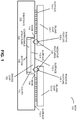
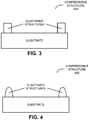
- FIG. 1 presents a block diagram illustrating a side view of an MCM 100.
- This MCM includes a substrate 110, island chips 120, a bridge chip 122 and a compressible structure 124.
- Substrate 110 has a surface 112-1 and a cavity 114 defined by an edge 116 in surface 112-1, where a bottom 118 of cavity 114 is vertically offset from surface 112-1.
- island chip 120-1 has a surface 112-2 that is mechanically and/or electrically coupled to surface 112-1 (for example, by C4 solder), and bridge chip 122 has surfaces 112-3 and 112-4, where surface 112-3 faces and partially overlaps surface 112-2.
- bridge chip 122 is positioned in cavity 114 and is mechanically and/or electrically coupled to island chips 120.
- bridge chip 122 may be electrically coupled to island chips 120 by (at least partially) overlapping proximity-communication ( P x C ) connectors on surfaces 112-2 and 112-3, such as: capacitive PxC connectors, inductive PxC connectors, conductive PxC connectors, and/or optical PxC connectors. As shown in FIG.
- the P x C connectors may include compression-compliant micro-spring connectors 210. Note that, while bridge chip 122 communicates with island chips 120 using PxC, bridge chip 122 may be powered directly by island chips 120 or independently by substrate 110 (for example, using wire bonds).
- bridge chip 122 when assembled in MCM 100, bridge chip 122 typically is pushed up against island chips 120 in order to minimize a gap between surfaces 112-2 and 112-3 (and, thus, between PxC connectors) and to make sure that 128-1 and 128-2 are engaged to provide lateral alignment.
- this force may be provided by compressible structure 124, which is positioned between bottom 118 of cavity 114 and surface 112-4 of bridge chip 122.
- this compressible structure includes a compliant material with shape and volume compression.
- compressible structure 124 When partially compressed, compressible structure 124 provides a force on bridge chip 122 so that surfaces 112-2 and 112-3 are approximately coplanar without bending bridge chip 122 ( e.g., without a vertical gap larger than 0.1-1 ⁇ m developing between island chips 120 and bridge chip 122), which may enable communication using the PxC connectors.
- compressible structure 124 may facilitate assembly and may help maintain (relative) alignment of components in MCM 100.
- compressible structure 124 can absorb stress, such as that associated with different coefficients of thermal expansion and lateral shear force, thereby increasing the reliability of MCM 100 during operation.
- compressible structure 124 is also separate from substrate 110. This allows compressible structure 124 to 'slide' laterally as positive features 128 engage and align themselves.
- MCM 100 may also include additional features that facilitate assembly and that may help maintain in-plane ( XY ) alignment of components.
- bridge chip 122 may be mechanically coupled to island chips 120 by pairs of negative features 126 on surfaces 112-2 and 112-3 and positive features 128 that mate with the corresponding pairs of negative features 126.
- negative features 126 may include pits that are recessed below surfaces 112-2 and 112-3, and positive features 128 may include spherical balls that mate with negative features 126 (such as a ball-and-etch-pit structure), thereby aligning island chips 120 and bridge chip 122.
- alignment in MCM 100 may be facilitated using positive features on surfaces 112-2 and 112-3, where these positive features protrude above these surfaces).
- the pairs of negative features 126 are proximate to corners of bridge chip 122 and island chips 120.
- mating negative features 126 and positive features 128 can provide highly accurate self-alignment in the XY plane of island chips 120 and bridge chip 122, as well as coplanarity control during assembly.
- the alignment over surfaces 112-2 and 112-3 may be within ⁇ 1 ⁇ m in the XY plane.
- components in MCM 100 are permanently attached after remateable alignment, for example, by using a post-alignment technique to permanently fix the chip-to-chip alignment.
- solder may be partially melted or reflowed at an elevated temperature to fuse components in MCM 100 to create a more permanent bond.
- components in MCM 100 are remateably coupled, thereby facilitating rework of MCM 100.
- MCM 100 includes four positive features 128 per bridge chip.
- compressible structure 124 may provide 1-2 pounds of compressive force per positive feature.
- Compressible structure 124 may have an uncompressed thickness of 100-200 ⁇ m and a compressed thickness of 50-60 ⁇ m when MCM 100 is assembled.
- cavity 114 may have a depth of 200-300 ⁇ m and bridge chip 122 may have a thickness of 150 ⁇ m. This reduced thickness of bridge chip 122 may reduce stiffness, but in conjunction with compressible structure 124, bridge chip 122 may remain 'flat' throughout assembly and operation of MCM 100.
- the compressible structure 124 may provide the necessary counter-forces in a uniform manner to a thinned bridge chip 122 preventing bowing of the bridge chip 122 or disrupting communication, such as P x C .
- changes in the vertical gap or spacing between surfaces 112-2 and 112-3 may be less than 10% of the nominal gap.
- a wide variety of features and shapes may be used to provide the force in compressible structure 124, including: a cylindrically shaped feature, an elliptically shaped bump, a hemispherically shaped bump, a truncated hemispherically shaped bump, a rectangularly shaped bump (such as a top hat), a pyramidally shaped bump, truncated pyramidally shaped bump and/or a follicle-shaped feature (for example, tilted finger-like structures). More generally, the compressible structure 124 may be other than a spring. According to the claimed invention, the compliant material in compressible structure 124 includes an elastomer.
- compliant material may be fabricated using an additive fabrication process in which material is deposited or, more generally, added. However, in other embodiments a subtractive process, in which material is removed, is used either separately or in conjunction with the additive process.
- substrate 110 may include: a semiconductor (such as silicon or a silicon-on-insulator wafer), an organic material, a ceramic, glass, and/or a plastic.
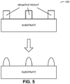
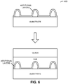
- bridge chip 122 may be placed face-up in cavity 114 (on top of substrate 110). In addition, if there are negative features 126 on surface 112-3, positive features 128 may be placed in negative features 126. Then, a mechanical fixture may push down on bridge chip 122 while island chips 120 are aligned and attached to substrate 110, for example, using a reflow-attachment process. Once the reflow cycle is complete, the external mechanical load on bridge chip 122 is released, causing bridge chip 122 to be pushed away from substrate 110 by compressible structure 124.
- This upward force may cause the ball-in-pit structure to be engaged with a predetermined amount of force (against a reference mechanical plane provided by island chips 120) that was targeted in the design of MCM 100.
- island chips 120 can be attached to substrate 110, yet can still move freely to maintain (relative) alignment of connectors on surfaces 112-2 and 112-3 over the life of MCM 100.
- bridge chip 122 includes micro-spring connectors 210 ( FIG. 2 ) to provide remateable electrical connections between island chips 120 and bridge chip 122.
- the force applied by compressible structure 124 may be larger than the force applied by micro-spring connectors 210 ( FIG. 2 ).
- the compressible structure may include an array of elastomeric structures (and, more generally, a compliant material) fabricated on a thin substrate.
- the shapes and sizes of the individual elastomeric structures may be varied to fit the needs of the MCM.
- the elastomeric structures may be cylindrical (ranging from low to high aspect ratios).
- the elastomeric structures may be hemispherical domes.
- a given compressible structure in the MCM may include single or multiple bumps at each desired location or may include an array of high-aspect ratio (hair-like) structures. These bumps may range in height from 50-500 ⁇ m and may be fabricated on a thin (50-200 ⁇ m) elastic substrate (such as tungsten foil, alumina, etc.).
- the substrate in the compressible structure may be thin, and flat to facilitate fabrication and to fit into cavities (such as cavity 114 in FIG. 1 ) without significantly increasing the form factor.
- the substrate in the compressible structure may be stiff to reduce chip warpage or bending when the mechanical fixture is disengaged during the assembly technique.
- the fabrication technique includes two principal operations: fabrication of the reusable molds; and fabrication of the compressible structures by stamping/molding.
- the shape of the compliant material such as the elastomeric bumps
- the shape of the compliant material may be determined (because the shapes created in the molds will be replicated onto the compliant material).
- bumps with different mechanical characteristics may be used depending on the MCM configuration.
- the number of bumps may be varied depending on the configuration.
- FIG. 5 presents a flow diagram 500 illustrating fabrication of a mold for a compressible structure.
- a negative photoresist for example, a 100 ⁇ m thick film of NR21
- a substrate such as silicon
- photolithography to yield positive photoresist features at the locations of the bumps.
- a positive photoresist may also be used.
- the photoresist features are reflowed using a thermal profile and transformed into hemispherical domes (such as domes having a diameter of 180 ⁇ m) with adequate adhesion to the substrate.
- FIG. 6 presents a flow diagram 600 illustrating fabrication of a mold for a compressible structure.
- a sacrificial layer process may be used to build the mold from the positive reflowed features shown in FIG. 5 .
- a titanium layer (which may have a thickness of 30 nm) and a gold layer (which may have a thickness of 300 nm) may be conformally deposited on the reflowed features.
- a negative-resist layer (which may have a thickness of 2 ⁇ m) and another set of titanium and gold layers may be deposited. As described further below, note that the negative-resist layer may make it easier to separate the components after the mold has been fabricated.
- a photoresist such as SU8
- SU8 may be poured over the positive dome structure and a glass substrate may be placed over the SU8. Then, the SU8 may be crosslinked by exposing it in UV light through the glass slide and placing the structure in an oven at 90 C for a post-exposure bake. Note that the glass substrate is not a part of the final mold. Instead, the glass substrate may act as a carrier for the SU8 mold. However, one of a variety of UV -transparent substrates can be used. In principle, this fabrication process may be performed on a large glass panel so that multiple molds can be fabricated in parallel. These molds may correspond to different designs.
- the mold can be separated by placing it on a 150 °C hot plate for few seconds. This may soften the negative-resist (sacrificial) layer and may make it easier to separate the mold from the positive features. Without this sacrificial-layer operation, the yield may be significantly reduced because the positive features may adhere to the mold. Once separated, the negative resist can also be cleaned and removed on both surfaces using appropriate solvents.
- FIG. 7 which presents a flow diagram 700 illustrating fabrication of a compressible structure
- an elastomeric material such as silicone or Sylgard® 160 (from Dow Corning Corporation, of Midland, MI)
- silicone or Sylgard® 160 from Dow Corning Corporation, of Midland, MI
- a thin substrate for example, tungsten plate with a thin SiO 2 layer
- a vertical force is exerted on the back of the compressible-structure substrate. This force may determine the thickness of the elastomer.
- the magnitude of the force should be high enough to yield a very thin base layer of elastomer.
- the sample may be placed in a vacuum chamber to degas the compliant material, and then in an oven to cure and harden.
- the compliant material Once the compliant material has cured and cooled to room temperature, it can be separated from the SU8 mold because SU8 and silicone typically have poor adhesion strength, while the silicone and the SiO 2 film on the Tungsten substrate usually have an excellent adhesion strength.
- the SiO 2 film may play an important function in this regard, because adhesion of silicone to tungsten is usually not very good.
- the negative resist can be cleaned and removed on both surfaces using one or more solvents.
- the compressible structure includes 200 ⁇ m high silicone bumps fabricated on a 100 ⁇ m thick tungsten foil.
- a large array of compressible structures may be fabricated simultaneously.
- the compressible structures may be diced to their final size using a wafer dicing technique.
- the molds may be reused to fabricate additional compressible structures.
- Embodiments of the MCM may be used in a wide variety of applications.
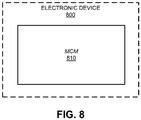
- a general application of an MCM is shown in FIG. 8 , which presents a block diagram illustrating an electronic device 800.
- This electronic device includes MCM 810, which may be MCM 100 ( FIG. 1 ) or 200 ( FIG. 2 ).
- FIG. 9 presents a block diagram illustrating a system 900 that includes one or more MCMs 908, such as MCM 100 ( FIG. 1 ) or 200 ( FIG. 2 ).
- System 900 may include: one or more processors 910, a communication interface 912 and a user interface 914, which may be coupled to other components in system 900 by one or more signal lines 922.
- the one or more processors (or processor cores) 910 may support parallel processing and/or multi-threaded operation
- the communication interface 912 may have a persistent communication connection
- the one or more signal lines 922 may constitute a communication bus.
- the user interface 914 may include: a display 916, a keyboard 918, and/or a pointer 920, such as a mouse.
- Memory 924 in system 900 may include volatile memory and/or non-volatile memory. More specifically, memory 924 may include: ROM, RAM, EPROM, EEPROM, flash, one or more smart cards, one or more magnetic disc storage devices, and/or one or more optical storage devices. Memory 924 may store an operating system 926 that includes procedures (or a set of instructions) for handling various basic system services for performing hardware-dependent tasks. Moreover, memory 924 may also store communications procedures (or a set of instructions) in a communication module 928. These communication procedures may be used for communicating with one or more computers, devices and/or servers, including computers, devices and/or servers that are remotely located with respect to the system 900.
- Memory 924 may also include one or more program modules 930 (or a set of instructions). Note that one or more of program modules 930 may constitute a computer-program mechanism. Instructions in the various modules in the memory 924 may be implemented in: a high-level procedural language, an object-oriented programming language, and/or in an assembly or machine language. The programming language may be compiled or interpreted, i.e., configurable or configured, to be executed by the one or more processors (or processor cores) 910.
- System 900 may include, but is not limited to: a server, a laptop computer, a communication device or system, a personal computer, a work station, a mainframe computer, a blade, an enterprise computer, a data center, a portable-computing device, a tablet computer, a cellular telephone, a supercomputer, a network-attached-storage (NAS) system, a storage-area-network (SAN ) system, an electronic device, and/or another electronic computing device.
- NAS network-attached-storage
- SAN storage-area-network
- embodiments of the one or more MCMs 908 may be used in a variety of applications, including: VLSI circuits, communication systems (such as in wavelength division multiplexing), storage area networks, data centers, networks (such as local area networks), and/or computer systems (such as multiple-core processor computer systems).
- the one or more MCMs 908 may be included in a backplane that is coupled to multiple processor blades, or the one or more MCMs 908 may couple different types of components (such as processors, memory, input/output devices, and/or peripheral devices).
- the one or more MCMs 908 may perform the functions of: a switch, a hub, a bridge, and/or a router.
- system 900 may be at one location or may be distributed over multiple, geographically dispersed locations. Moreover, some or all of the functionality of system 900 may be implemented in one or more application-specific integrated circuits ( ASICs ) and/or one or more digital signal processors ( DSPs ) . Furthermore, functionality in the preceding embodiments may be implemented more in hardware and less in software, or less in hardware and more in software, as is known in the art.
- ASICs application-specific integrated circuits
- DSPs digital signal processors
- the preceding embodiments may include fewer components or additional components.
- island chips 120 may be electrically coupled to substrate 110 using micro-spring connectors.
- an external clamping force may be applied to MCM 100 to hold the chips together.
- the MCM and system are illustrated as having a number of discrete items, these embodiments are intended to be functional descriptions of the various features that may be present rather than structural schematics of the embodiments described herein. Consequently, in these embodiments, two or more components may be combined into a single component and/or a position of one or more components may be changed. Furthermore, features in two or more of the preceding embodiments may be combined with one another.
- surfaces on components should be understood to include surfaces of substrates or surfaces of layers deposited on these substrates (such as a dielectric layer deposited on a substrate).
- components in the MCM may be fabricated, and the MCM may be assembled, using a wide variety of techniques, as is known to one of skill in the art.
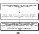
- FIG. 10 presents a flow diagram 1000 illustrating a method for maintaining alignment of an island chip and a bridge chip in an MCM, such as MCM 100 ( FIG. 1 ) or 200 ( FIG. 2 ).
- a compressible structure is positioned in a cavity, defined by an edge, in a first surface of a substrate in the MCM (operation 1010), where the compressible structure includes a compliant material with shape and volume compression, and where a bottom of the cavity is vertically offset from the first surface.
- a bridge chip which has a third surface and a fourth surface (on an opposite side of the bridge chip from the third surface), is positioned in the cavity on top of the compressible structure (operation 1012), where the fourth surface is mechanically coupled to the compressible structure.
- an island chip having a second surface, is mechanically coupled to the first surface and the third surface (operation 1014), where the compressible structure provides a force on the bridge chip so that the second surface and the third surface are approximately coplanar without bending the bridge chip.
- method 1000 includes additional or fewer operations. Moreover, the order of the operations may be changed, and/or two or more operations may be combined into a single operation..
Landscapes
- Engineering & Computer Science (AREA)
- Microelectronics & Electronic Packaging (AREA)
- Power Engineering (AREA)
- Computer Hardware Design (AREA)
- Condensed Matter Physics & Semiconductors (AREA)
- General Physics & Mathematics (AREA)
- Physics & Mathematics (AREA)
- Manufacturing & Machinery (AREA)
- Micromachines (AREA)
- Wire Bonding (AREA)
- Internal Circuitry In Semiconductor Integrated Circuit Devices (AREA)
- Coupling Device And Connection With Printed Circuit (AREA)
- Connector Housings Or Holding Contact Members (AREA)
Applications Claiming Priority (2)
| Application Number | Priority Date | Filing Date | Title |
|---|---|---|---|
| US13/397,593 US8742576B2 (en) | 2012-02-15 | 2012-02-15 | Maintaining alignment in a multi-chip module using a compressible structure |
| PCT/US2013/026223 WO2013123259A2 (en) | 2012-02-15 | 2013-02-14 | Maintaining alignment in a multi-chip module using a compressible structure |
Publications (2)
| Publication Number | Publication Date |
|---|---|
| EP2815429A2 EP2815429A2 (en) | 2014-12-24 |
| EP2815429B1 true EP2815429B1 (en) | 2021-07-07 |
Family
ID=47790523
Family Applications (1)
| Application Number | Title | Priority Date | Filing Date |
|---|---|---|---|
| EP13749252.6A Active EP2815429B1 (en) | 2012-02-15 | 2013-02-14 | Multi-chip module comprising a compressible structure and method for maintaining alignment in a multi-chip module using a compressible structure |
Country Status (6)
| Country | Link |
|---|---|
| US (1) | US8742576B2 (enExample) |
| EP (1) | EP2815429B1 (enExample) |
| JP (1) | JP6182548B2 (enExample) |
| CN (1) | CN104471709B (enExample) |
| TW (1) | TWI550821B (enExample) |
| WO (1) | WO2013123259A2 (enExample) |
Families Citing this family (51)
| Publication number | Priority date | Publication date | Assignee | Title |
|---|---|---|---|---|
| US8569652B2 (en) | 2009-11-17 | 2013-10-29 | Illinois Tool Works Inc. | Incremental hybrid welding systems and methods |
| US8482111B2 (en) | 2010-07-19 | 2013-07-09 | Tessera, Inc. | Stackable molded microelectronic packages |
| KR101128063B1 (ko) | 2011-05-03 | 2012-04-23 | 테세라, 인코포레이티드 | 캡슐화 층의 표면에 와이어 본드를 구비하는 패키지 적층형 어셈블리 |
| US8404520B1 (en) | 2011-10-17 | 2013-03-26 | Invensas Corporation | Package-on-package assembly with wire bond vias |
| US8946757B2 (en) | 2012-02-17 | 2015-02-03 | Invensas Corporation | Heat spreading substrate with embedded interconnects |
| US8835228B2 (en) | 2012-05-22 | 2014-09-16 | Invensas Corporation | Substrate-less stackable package with wire-bond interconnect |
| US9502390B2 (en) | 2012-08-03 | 2016-11-22 | Invensas Corporation | BVA interposer |
| US9167710B2 (en) | 2013-08-07 | 2015-10-20 | Invensas Corporation | Embedded packaging with preformed vias |
| US20150076714A1 (en) | 2013-09-16 | 2015-03-19 | Invensas Corporation | Microelectronic element with bond elements to encapsulation surface |
| US9583456B2 (en) | 2013-11-22 | 2017-02-28 | Invensas Corporation | Multiple bond via arrays of different wire heights on a same substrate |
| US9263394B2 (en) | 2013-11-22 | 2016-02-16 | Invensas Corporation | Multiple bond via arrays of different wire heights on a same substrate |
| US9379074B2 (en) * | 2013-11-22 | 2016-06-28 | Invensas Corporation | Die stacks with one or more bond via arrays of wire bond wires and with one or more arrays of bump interconnects |
| US9583411B2 (en) | 2014-01-17 | 2017-02-28 | Invensas Corporation | Fine pitch BVA using reconstituted wafer with area array accessible for testing |
| KR101815489B1 (ko) * | 2014-02-26 | 2018-01-05 | 인텔 코포레이션 | 스루 브리지 도전성 비아 신호 접속에 의한 임베딩된 멀티디바이스 브리지 |
| US10381326B2 (en) | 2014-05-28 | 2019-08-13 | Invensas Corporation | Structure and method for integrated circuits packaging with increased density |
| US9735084B2 (en) | 2014-12-11 | 2017-08-15 | Invensas Corporation | Bond via array for thermal conductivity |
| US9379090B1 (en) * | 2015-02-13 | 2016-06-28 | Qualcomm Incorporated | System, apparatus, and method for split die interconnection |
| US9888579B2 (en) | 2015-03-05 | 2018-02-06 | Invensas Corporation | Pressing of wire bond wire tips to provide bent-over tips |
| US9443824B1 (en) | 2015-03-30 | 2016-09-13 | Qualcomm Incorporated | Cavity bridge connection for die split architecture |
| US9653428B1 (en) * | 2015-04-14 | 2017-05-16 | Amkor Technology, Inc. | Semiconductor package and fabricating method thereof |
| US9502372B1 (en) | 2015-04-30 | 2016-11-22 | Invensas Corporation | Wafer-level packaging using wire bond wires in place of a redistribution layer |
| US9761554B2 (en) | 2015-05-07 | 2017-09-12 | Invensas Corporation | Ball bonding metal wire bond wires to metal pads |
| US9490222B1 (en) | 2015-10-12 | 2016-11-08 | Invensas Corporation | Wire bond wires for interference shielding |
| US10490528B2 (en) | 2015-10-12 | 2019-11-26 | Invensas Corporation | Embedded wire bond wires |
| US10332854B2 (en) | 2015-10-23 | 2019-06-25 | Invensas Corporation | Anchoring structure of fine pitch bva |
| US10181457B2 (en) | 2015-10-26 | 2019-01-15 | Invensas Corporation | Microelectronic package for wafer-level chip scale packaging with fan-out |
| US9911718B2 (en) | 2015-11-17 | 2018-03-06 | Invensas Corporation | ‘RDL-First’ packaged microelectronic device for a package-on-package device |
| US9984992B2 (en) | 2015-12-30 | 2018-05-29 | Invensas Corporation | Embedded wire bond wires for vertical integration with separate surface mount and wire bond mounting surfaces |
| US10312220B2 (en) | 2016-01-27 | 2019-06-04 | Amkor Technology, Inc. | Semiconductor package and fabricating method thereof |
| TWI652778B (zh) | 2016-01-27 | 2019-03-01 | Amkor Technology, Inc. | 半導體封裝以及其製造方法 |
| US10497674B2 (en) | 2016-01-27 | 2019-12-03 | Amkor Technology, Inc. | Semiconductor package and fabricating method thereof |
| US9698564B1 (en) * | 2016-02-09 | 2017-07-04 | Oracle International Corporation | Hybrid integrated MCM with waveguide-fiber connector |
| US9978686B1 (en) * | 2016-02-19 | 2018-05-22 | The United States Of America As Represented By The Administrator Of National Aeronautics And Space Administration | Interconnection of semiconductor devices in extreme environment microelectronic integrated circuit chips |
| US9935075B2 (en) | 2016-07-29 | 2018-04-03 | Invensas Corporation | Wire bonding method and apparatus for electromagnetic interference shielding |
| KR102632563B1 (ko) | 2016-08-05 | 2024-02-02 | 삼성전자주식회사 | 반도체 패키지 |
| US10299368B2 (en) | 2016-12-21 | 2019-05-21 | Invensas Corporation | Surface integrated waveguides and circuit structures therefor |
| KR20180086804A (ko) | 2017-01-23 | 2018-08-01 | 앰코 테크놀로지 인코포레이티드 | 반도체 디바이스 및 그 제조 방법 |
| US10475766B2 (en) * | 2017-03-29 | 2019-11-12 | Intel Corporation | Microelectronics package providing increased memory component density |
| US20190006331A1 (en) * | 2017-06-30 | 2019-01-03 | Intel Corporation | Electronics package devices with through-substrate-vias having pitches independent of substrate thickness |
| US10840205B2 (en) | 2017-09-24 | 2020-11-17 | Invensas Bonding Technologies, Inc. | Chemical mechanical polishing for hybrid bonding |
| US11289424B2 (en) * | 2018-11-29 | 2022-03-29 | Taiwan Semiconductor Manufacturing Company, Ltd. | Package and method of manufacturing the same |
| KR102538704B1 (ko) * | 2018-12-04 | 2023-06-01 | 에스케이하이닉스 주식회사 | 플렉시블 브리지 다이를 포함한 스택 패키지 |
| US11676941B2 (en) | 2018-12-07 | 2023-06-13 | Amkor Technology Singapore Holding Pte. Ltd. | Semiconductor package and fabricating method thereof |
| US12154858B2 (en) * | 2019-06-19 | 2024-11-26 | Invensas Llc | Connecting multiple chips using an interconnect device |
| US11569172B2 (en) | 2019-08-08 | 2023-01-31 | Taiwan Semiconductor Manufacturing Co., Ltd. | Semiconductor devices and methods of manufacture |
| KR102674087B1 (ko) * | 2019-09-06 | 2024-06-12 | 에스케이하이닉스 주식회사 | 전자기간섭 차폐층을 포함하는 반도체 패키지 |
| CN113140520B (zh) * | 2020-01-19 | 2024-11-08 | 江苏长电科技股份有限公司 | 封装结构及其成型方法 |
| JP7226358B2 (ja) * | 2020-02-05 | 2023-02-21 | 株式会社デンソー | 電子機器 |
| US11804469B2 (en) | 2020-05-07 | 2023-10-31 | Invensas Llc | Active bridging apparatus |
| US11264357B1 (en) | 2020-10-20 | 2022-03-01 | Invensas Corporation | Mixed exposure for large die |
| US20250273548A1 (en) * | 2024-02-28 | 2025-08-28 | Qualcomm Incorporated | Package comprising a bridge with spring pads |
Citations (1)
| Publication number | Priority date | Publication date | Assignee | Title |
|---|---|---|---|---|
| US20090244874A1 (en) * | 2008-03-31 | 2009-10-01 | Ravi Mahajan | Microelectronic package containing silicon patches for high density interconnects, and method of manufacturing same |
Family Cites Families (14)
| Publication number | Priority date | Publication date | Assignee | Title |
|---|---|---|---|---|
| DE4242565C1 (de) * | 1992-12-16 | 1994-03-17 | Deutsche Aerospace | Verfahren zur Justage von Halbleiterscheiben zueinander |
| JP4167443B2 (ja) * | 2002-01-30 | 2008-10-15 | 日本放送協会 | 固体撮像素子 |
| US7525199B1 (en) | 2004-05-21 | 2009-04-28 | Sun Microsystems, Inc | Packaging for proximity communication positioned integrated circuits |
| US7893531B2 (en) * | 2007-09-28 | 2011-02-22 | Oracle America, Inc. | Integrated-circuit package for proximity communication |
| US8227904B2 (en) | 2009-06-24 | 2012-07-24 | Intel Corporation | Multi-chip package and method of providing die-to-die interconnects in same |
| US8531042B2 (en) * | 2009-06-30 | 2013-09-10 | Oracle America, Inc. | Technique for fabricating microsprings on non-planar surfaces |
| US8487429B2 (en) | 2009-09-22 | 2013-07-16 | Oracle America, Inc. | Assembly of multi-chip modules using sacrificial features |
| US8188581B2 (en) * | 2009-09-28 | 2012-05-29 | Oracle America, Inc. | Mechanical coupling in a multi-chip module using magnetic components |
| US8315065B2 (en) * | 2009-09-28 | 2012-11-20 | Oracle America, Inc. | Self-locking features in a multi-chip module |
| US8212354B2 (en) | 2009-12-17 | 2012-07-03 | Oracle America, Inc. | Active plastic bridge chips |
| US8218334B2 (en) * | 2010-03-09 | 2012-07-10 | Oracle America, Inc. | Multi-chip module with multi-level interposer |
| US8698322B2 (en) * | 2010-03-24 | 2014-04-15 | Oracle International Corporation | Adhesive-bonded substrates in a multi-chip module |
| US8274149B2 (en) * | 2010-03-29 | 2012-09-25 | Advanced Semiconductor Engineering, Inc. | Semiconductor device package having a buffer structure and method of fabricating the same |
| US8648463B2 (en) * | 2010-05-17 | 2014-02-11 | Oracle International Corporation | Assembly of multi-chip modules with proximity connectors using reflowable features |
-
2012
- 2012-02-15 US US13/397,593 patent/US8742576B2/en active Active
-
2013
- 2013-02-08 TW TW102105343A patent/TWI550821B/zh active
- 2013-02-14 CN CN201380009348.0A patent/CN104471709B/zh active Active
- 2013-02-14 JP JP2014557785A patent/JP6182548B2/ja active Active
- 2013-02-14 WO PCT/US2013/026223 patent/WO2013123259A2/en not_active Ceased
- 2013-02-14 EP EP13749252.6A patent/EP2815429B1/en active Active
Patent Citations (1)
| Publication number | Priority date | Publication date | Assignee | Title |
|---|---|---|---|---|
| US20090244874A1 (en) * | 2008-03-31 | 2009-10-01 | Ravi Mahajan | Microelectronic package containing silicon patches for high density interconnects, and method of manufacturing same |
Also Published As
| Publication number | Publication date |
|---|---|
| WO2013123259A2 (en) | 2013-08-22 |
| JP6182548B2 (ja) | 2017-08-16 |
| US8742576B2 (en) | 2014-06-03 |
| JP2015524155A (ja) | 2015-08-20 |
| CN104471709B (zh) | 2018-11-16 |
| TW201401480A (zh) | 2014-01-01 |
| EP2815429A2 (en) | 2014-12-24 |
| US20130207261A1 (en) | 2013-08-15 |
| CN104471709A (zh) | 2015-03-25 |
| TWI550821B (zh) | 2016-09-21 |
| WO2013123259A3 (en) | 2014-11-13 |
| WO2013123259A9 (en) | 2015-08-13 |
Similar Documents
| Publication | Publication Date | Title |
|---|---|---|
| EP2815429B1 (en) | Multi-chip module comprising a compressible structure and method for maintaining alignment in a multi-chip module using a compressible structure | |
| US9281268B2 (en) | Method for fabricating multi-chip module with multi-level interposer | |
| US8975754B2 (en) | Chip package for high-count chip stacks | |
| US20240337799A1 (en) | Co-Packaging Assembly and Method for Attaching Photonic Dies/Modules to Multi-Chip Active/Passive Substrate | |
| EP2201602B1 (en) | Alignment features for proximity communication | |
| CN107622957B (zh) | 双面SiP的三维封装结构的制造方法 | |
| US8164917B2 (en) | Base plate for use in a multi-chip module | |
| US8531042B2 (en) | Technique for fabricating microsprings on non-planar surfaces | |
| US9111943B2 (en) | Alignment structures for integrated-circuit packaging | |
| US20190287944A1 (en) | Asics face to face self assembly | |
| US20140225284A1 (en) | Low-cost chip package for chip stacks | |
| US8698322B2 (en) | Adhesive-bonded substrates in a multi-chip module | |
| US8487429B2 (en) | Assembly of multi-chip modules using sacrificial features | |
| EP2973670B1 (en) | Method for fabricating a multi-chip module with self-populating positive features | |
| US8659161B2 (en) | Chip package with reinforced positive alignment features | |
| US20250293223A1 (en) | Electronic package and manufacturing method thereof | |
| TWI892184B (zh) | 包括虛設條的封裝以及形成所述封裝的方法 | |
| US8315065B2 (en) | Self-locking features in a multi-chip module | |
| Yang et al. | Assembly and alignment of Proximity Communication enabled multi-chip packages using elastomeric bump interposers |
Legal Events
| Date | Code | Title | Description |
|---|---|---|---|
| PUAI | Public reference made under article 153(3) epc to a published international application that has entered the european phase |
Free format text: ORIGINAL CODE: 0009012 |
|
| 17P | Request for examination filed |
Effective date: 20140815 |
|
| AK | Designated contracting states |
Kind code of ref document: A2 Designated state(s): AL AT BE BG CH CY CZ DE DK EE ES FI FR GB GR HR HU IE IS IT LI LT LU LV MC MK MT NL NO PL PT RO RS SE SI SK SM TR |
|
| AX | Request for extension of the european patent |
Extension state: BA ME |
|
| RIC1 | Information provided on ipc code assigned before grant |
Ipc: H01L 25/065 20060101AFI20150603BHEP Ipc: H01L 23/48 20060101ALI20150603BHEP |
|
| DAX | Request for extension of the european patent (deleted) | ||
| STAA | Information on the status of an ep patent application or granted ep patent |
Free format text: STATUS: EXAMINATION IS IN PROGRESS |
|
| 17Q | First examination report despatched |
Effective date: 20190121 |
|
| GRAP | Despatch of communication of intention to grant a patent |
Free format text: ORIGINAL CODE: EPIDOSNIGR1 |
|
| STAA | Information on the status of an ep patent application or granted ep patent |
Free format text: STATUS: GRANT OF PATENT IS INTENDED |
|
| INTG | Intention to grant announced |
Effective date: 20210210 |
|
| GRAS | Grant fee paid |
Free format text: ORIGINAL CODE: EPIDOSNIGR3 |
|
| GRAA | (expected) grant |
Free format text: ORIGINAL CODE: 0009210 |
|
| STAA | Information on the status of an ep patent application or granted ep patent |
Free format text: STATUS: THE PATENT HAS BEEN GRANTED |
|
| AK | Designated contracting states |
Kind code of ref document: B1 Designated state(s): AL AT BE BG CH CY CZ DE DK EE ES FI FR GB GR HR HU IE IS IT LI LT LU LV MC MK MT NL NO PL PT RO RS SE SI SK SM TR |
|
| REG | Reference to a national code |
Ref country code: GB Ref legal event code: FG4D |
|
| REG | Reference to a national code |
Ref country code: AT Ref legal event code: REF Ref document number: 1409416 Country of ref document: AT Kind code of ref document: T Effective date: 20210715 |
|
| REG | Reference to a national code |
Ref country code: DE Ref legal event code: R096 Ref document number: 602013078250 Country of ref document: DE |
|
| REG | Reference to a national code |
Ref country code: IE Ref legal event code: FG4D |
|
| REG | Reference to a national code |
Ref country code: LT Ref legal event code: MG9D |
|
| REG | Reference to a national code |
Ref country code: NL Ref legal event code: MP Effective date: 20210707 |
|
| REG | Reference to a national code |
Ref country code: AT Ref legal event code: MK05 Ref document number: 1409416 Country of ref document: AT Kind code of ref document: T Effective date: 20210707 |
|
| PG25 | Lapsed in a contracting state [announced via postgrant information from national office to epo] |
Ref country code: HR Free format text: LAPSE BECAUSE OF FAILURE TO SUBMIT A TRANSLATION OF THE DESCRIPTION OR TO PAY THE FEE WITHIN THE PRESCRIBED TIME-LIMIT Effective date: 20210707 Ref country code: SE Free format text: LAPSE BECAUSE OF FAILURE TO SUBMIT A TRANSLATION OF THE DESCRIPTION OR TO PAY THE FEE WITHIN THE PRESCRIBED TIME-LIMIT Effective date: 20210707 Ref country code: ES Free format text: LAPSE BECAUSE OF FAILURE TO SUBMIT A TRANSLATION OF THE DESCRIPTION OR TO PAY THE FEE WITHIN THE PRESCRIBED TIME-LIMIT Effective date: 20210707 Ref country code: FI Free format text: LAPSE BECAUSE OF FAILURE TO SUBMIT A TRANSLATION OF THE DESCRIPTION OR TO PAY THE FEE WITHIN THE PRESCRIBED TIME-LIMIT Effective date: 20210707 Ref country code: NO Free format text: LAPSE BECAUSE OF FAILURE TO SUBMIT A TRANSLATION OF THE DESCRIPTION OR TO PAY THE FEE WITHIN THE PRESCRIBED TIME-LIMIT Effective date: 20211007 Ref country code: NL Free format text: LAPSE BECAUSE OF FAILURE TO SUBMIT A TRANSLATION OF THE DESCRIPTION OR TO PAY THE FEE WITHIN THE PRESCRIBED TIME-LIMIT Effective date: 20210707 Ref country code: PT Free format text: LAPSE BECAUSE OF FAILURE TO SUBMIT A TRANSLATION OF THE DESCRIPTION OR TO PAY THE FEE WITHIN THE PRESCRIBED TIME-LIMIT Effective date: 20211108 Ref country code: RS Free format text: LAPSE BECAUSE OF FAILURE TO SUBMIT A TRANSLATION OF THE DESCRIPTION OR TO PAY THE FEE WITHIN THE PRESCRIBED TIME-LIMIT Effective date: 20210707 Ref country code: BG Free format text: LAPSE BECAUSE OF FAILURE TO SUBMIT A TRANSLATION OF THE DESCRIPTION OR TO PAY THE FEE WITHIN THE PRESCRIBED TIME-LIMIT Effective date: 20211007 Ref country code: AT Free format text: LAPSE BECAUSE OF FAILURE TO SUBMIT A TRANSLATION OF THE DESCRIPTION OR TO PAY THE FEE WITHIN THE PRESCRIBED TIME-LIMIT Effective date: 20210707 Ref country code: LT Free format text: LAPSE BECAUSE OF FAILURE TO SUBMIT A TRANSLATION OF THE DESCRIPTION OR TO PAY THE FEE WITHIN THE PRESCRIBED TIME-LIMIT Effective date: 20210707 |
|
| PG25 | Lapsed in a contracting state [announced via postgrant information from national office to epo] |
Ref country code: PL Free format text: LAPSE BECAUSE OF FAILURE TO SUBMIT A TRANSLATION OF THE DESCRIPTION OR TO PAY THE FEE WITHIN THE PRESCRIBED TIME-LIMIT Effective date: 20210707 Ref country code: LV Free format text: LAPSE BECAUSE OF FAILURE TO SUBMIT A TRANSLATION OF THE DESCRIPTION OR TO PAY THE FEE WITHIN THE PRESCRIBED TIME-LIMIT Effective date: 20210707 Ref country code: GR Free format text: LAPSE BECAUSE OF FAILURE TO SUBMIT A TRANSLATION OF THE DESCRIPTION OR TO PAY THE FEE WITHIN THE PRESCRIBED TIME-LIMIT Effective date: 20211008 |
|
| REG | Reference to a national code |
Ref country code: DE Ref legal event code: R097 Ref document number: 602013078250 Country of ref document: DE |
|
| PG25 | Lapsed in a contracting state [announced via postgrant information from national office to epo] |
Ref country code: DK Free format text: LAPSE BECAUSE OF FAILURE TO SUBMIT A TRANSLATION OF THE DESCRIPTION OR TO PAY THE FEE WITHIN THE PRESCRIBED TIME-LIMIT Effective date: 20210707 |
|
| PLBE | No opposition filed within time limit |
Free format text: ORIGINAL CODE: 0009261 |
|
| STAA | Information on the status of an ep patent application or granted ep patent |
Free format text: STATUS: NO OPPOSITION FILED WITHIN TIME LIMIT |
|
| PG25 | Lapsed in a contracting state [announced via postgrant information from national office to epo] |
Ref country code: SM Free format text: LAPSE BECAUSE OF FAILURE TO SUBMIT A TRANSLATION OF THE DESCRIPTION OR TO PAY THE FEE WITHIN THE PRESCRIBED TIME-LIMIT Effective date: 20210707 Ref country code: SK Free format text: LAPSE BECAUSE OF FAILURE TO SUBMIT A TRANSLATION OF THE DESCRIPTION OR TO PAY THE FEE WITHIN THE PRESCRIBED TIME-LIMIT Effective date: 20210707 Ref country code: RO Free format text: LAPSE BECAUSE OF FAILURE TO SUBMIT A TRANSLATION OF THE DESCRIPTION OR TO PAY THE FEE WITHIN THE PRESCRIBED TIME-LIMIT Effective date: 20210707 Ref country code: EE Free format text: LAPSE BECAUSE OF FAILURE TO SUBMIT A TRANSLATION OF THE DESCRIPTION OR TO PAY THE FEE WITHIN THE PRESCRIBED TIME-LIMIT Effective date: 20210707 Ref country code: CZ Free format text: LAPSE BECAUSE OF FAILURE TO SUBMIT A TRANSLATION OF THE DESCRIPTION OR TO PAY THE FEE WITHIN THE PRESCRIBED TIME-LIMIT Effective date: 20210707 Ref country code: AL Free format text: LAPSE BECAUSE OF FAILURE TO SUBMIT A TRANSLATION OF THE DESCRIPTION OR TO PAY THE FEE WITHIN THE PRESCRIBED TIME-LIMIT Effective date: 20210707 |
|
| 26N | No opposition filed |
Effective date: 20220408 |
|
| PG25 | Lapsed in a contracting state [announced via postgrant information from national office to epo] |
Ref country code: IT Free format text: LAPSE BECAUSE OF FAILURE TO SUBMIT A TRANSLATION OF THE DESCRIPTION OR TO PAY THE FEE WITHIN THE PRESCRIBED TIME-LIMIT Effective date: 20210707 |
|
| PG25 | Lapsed in a contracting state [announced via postgrant information from national office to epo] |
Ref country code: MC Free format text: LAPSE BECAUSE OF FAILURE TO SUBMIT A TRANSLATION OF THE DESCRIPTION OR TO PAY THE FEE WITHIN THE PRESCRIBED TIME-LIMIT Effective date: 20210707 |
|
| REG | Reference to a national code |
Ref country code: CH Ref legal event code: PL |
|
| REG | Reference to a national code |
Ref country code: BE Ref legal event code: MM Effective date: 20220228 |
|
| PG25 | Lapsed in a contracting state [announced via postgrant information from national office to epo] |
Ref country code: LU Free format text: LAPSE BECAUSE OF NON-PAYMENT OF DUE FEES Effective date: 20220214 |
|
| PG25 | Lapsed in a contracting state [announced via postgrant information from national office to epo] |
Ref country code: FR Free format text: LAPSE BECAUSE OF NON-PAYMENT OF DUE FEES Effective date: 20220228 |
|
| PG25 | Lapsed in a contracting state [announced via postgrant information from national office to epo] |
Ref country code: LI Free format text: LAPSE BECAUSE OF NON-PAYMENT OF DUE FEES Effective date: 20220228 Ref country code: IE Free format text: LAPSE BECAUSE OF NON-PAYMENT OF DUE FEES Effective date: 20220214 Ref country code: CH Free format text: LAPSE BECAUSE OF NON-PAYMENT OF DUE FEES Effective date: 20220228 |
|
| PG25 | Lapsed in a contracting state [announced via postgrant information from national office to epo] |
Ref country code: BE Free format text: LAPSE BECAUSE OF NON-PAYMENT OF DUE FEES Effective date: 20220228 |
|
| P01 | Opt-out of the competence of the unified patent court (upc) registered |
Effective date: 20230522 |
|
| PG25 | Lapsed in a contracting state [announced via postgrant information from national office to epo] |
Ref country code: HU Free format text: LAPSE BECAUSE OF FAILURE TO SUBMIT A TRANSLATION OF THE DESCRIPTION OR TO PAY THE FEE WITHIN THE PRESCRIBED TIME-LIMIT; INVALID AB INITIO Effective date: 20130214 |
|
| PG25 | Lapsed in a contracting state [announced via postgrant information from national office to epo] |
Ref country code: MK Free format text: LAPSE BECAUSE OF FAILURE TO SUBMIT A TRANSLATION OF THE DESCRIPTION OR TO PAY THE FEE WITHIN THE PRESCRIBED TIME-LIMIT Effective date: 20210707 Ref country code: CY Free format text: LAPSE BECAUSE OF FAILURE TO SUBMIT A TRANSLATION OF THE DESCRIPTION OR TO PAY THE FEE WITHIN THE PRESCRIBED TIME-LIMIT Effective date: 20210707 |
|
| PG25 | Lapsed in a contracting state [announced via postgrant information from national office to epo] |
Ref country code: MT Free format text: LAPSE BECAUSE OF FAILURE TO SUBMIT A TRANSLATION OF THE DESCRIPTION OR TO PAY THE FEE WITHIN THE PRESCRIBED TIME-LIMIT Effective date: 20210707 |
|
| REG | Reference to a national code |
Ref country code: DE Ref legal event code: R079 Ref document number: 602013078250 Country of ref document: DE Free format text: PREVIOUS MAIN CLASS: H01L0025065000 Ipc: H10D0080300000 |
|
| PGFP | Annual fee paid to national office [announced via postgrant information from national office to epo] |
Ref country code: DE Payment date: 20241231 Year of fee payment: 13 |
|
| PGFP | Annual fee paid to national office [announced via postgrant information from national office to epo] |
Ref country code: GB Payment date: 20250102 Year of fee payment: 13 |
|
| PG25 | Lapsed in a contracting state [announced via postgrant information from national office to epo] |
Ref country code: TR Free format text: LAPSE BECAUSE OF FAILURE TO SUBMIT A TRANSLATION OF THE DESCRIPTION OR TO PAY THE FEE WITHIN THE PRESCRIBED TIME-LIMIT Effective date: 20210707 |