EP2813868B1 - Verfahren zur Synchronisation optischer Einheiten einer Lichtschranke und Lichtvorhang - Google Patents
Verfahren zur Synchronisation optischer Einheiten einer Lichtschranke und Lichtvorhang Download PDFInfo
- Publication number
- EP2813868B1 EP2813868B1 EP13171484.2A EP13171484A EP2813868B1 EP 2813868 B1 EP2813868 B1 EP 2813868B1 EP 13171484 A EP13171484 A EP 13171484A EP 2813868 B1 EP2813868 B1 EP 2813868B1
- Authority
- EP
- European Patent Office
- Prior art keywords
- optical
- optical unit
- synchronization
- signal
- synchronization signal
- Prior art date
- Legal status (The legal status is an assumption and is not a legal conclusion. Google has not performed a legal analysis and makes no representation as to the accuracy of the status listed.)
- Active
Links
Images


Classifications
-
- G—PHYSICS
- G01—MEASURING; TESTING
- G01V—GEOPHYSICS; GRAVITATIONAL MEASUREMENTS; DETECTING MASSES OR OBJECTS; TAGS
- G01V8/00—Prospecting or detecting by optical means
- G01V8/10—Detecting, e.g. by using light barriers
- G01V8/20—Detecting, e.g. by using light barriers using multiple transmitters or receivers
-
- G—PHYSICS
- G01—MEASURING; TESTING
- G01V—GEOPHYSICS; GRAVITATIONAL MEASUREMENTS; DETECTING MASSES OR OBJECTS; TAGS
- G01V8/00—Prospecting or detecting by optical means
- G01V8/10—Detecting, e.g. by using light barriers
-
- G—PHYSICS
- G06—COMPUTING OR CALCULATING; COUNTING
- G06F—ELECTRIC DIGITAL DATA PROCESSING
- G06F3/00—Input arrangements for transferring data to be processed into a form capable of being handled by the computer; Output arrangements for transferring data from processing unit to output unit, e.g. interface arrangements
- G06F3/01—Input arrangements or combined input and output arrangements for interaction between user and computer
- G06F3/03—Arrangements for converting the position or the displacement of a member into a coded form
- G06F3/041—Digitisers, e.g. for touch screens or touch pads, characterised by the transducing means
- G06F3/042—Digitisers, e.g. for touch screens or touch pads, characterised by the transducing means by opto-electronic means
- G06F3/0421—Digitisers, e.g. for touch screens or touch pads, characterised by the transducing means by opto-electronic means by interrupting or reflecting a light beam, e.g. optical touch-screen
Definitions
- the present invention relates to light curtains and photoelectric barriers, in particular safety light curtains, for monitoring a protective field, in particular to such light curtains which comprise a plurality of optoelectronic components interconnected by a communication bus.
- the present invention relates to a method for synchronizing the optical units of a photoelectric barrier and to such a photoelectric barrier.
- photoelectric barriers also referred to as light curtains or light grids, detect the movement or intrusion of objects into guarded zones, and more particularly, provide protection for human operators who are working with machines or other industrial equipment.
- Light curtains employing infrared or visible light beams are used to provide operator safety in a variety of industrial applications.
- Light curtains typically are employed for operator protection around machinery, such as punch presses, brakes, molding machines, automatic assembly equipment, coil winding machinery, robot operation, casting operations and the like.
- Conventional light curtains typically employ light emitting diodes (LED) mounted at spaced positions along a transmitter bar at one side of the guard zone and phototransistors (PT), photodiodes or photoreceivers mounted along a receiver bar at the opposite side of the zone.
- the LEDs transmit modulated infrared light beams along separate parallel channels to the PTs at the receiver bar. If one or more beams are blocked by an opaque object, such as the operator's arm, a control circuit either shuts the machine down, prevents the machine from cycling, or otherwise safeguards the area.
- safety light curtains comprise two optical units (also called bars, sticks, edges or strips), which are formed as two different constructional units, one of the optical units having the functionality of an emitter and one of a receiver.
- This dedicated architecture of an emitter and receiver has several drawbacks.
- the fabrication costs are high, because each type of optical unit has to be fabricated differently. Further, due to the fact that the optical communication is only unidirectional, i.e. from the sender to the receiver, the optical synchronization may be difficult and a transmission of communication information is possible only in one direction.
- the light curtain has two identical transmitting/receiving strips, to which transmitting and receiving units are fixed.
- the transmitting/receiving strips are placed opposite to each other with a protective field being formed between the strips.
- the transmitting/receiving strips are identically formed in control and evaluation units.
- the control and evaluation units have safety outputs, which are formed together as a switching channel.
- An identical power supply is provided for all the strips.
- photoelectric barriers often have the function of a so-called blanking, meaning that one or two radiation beams can be disabled in order to allow larger objects to pass through the sensing field without causing an alarm signal. Effectively, this blanking changes intermediately the minimum object resolution of the light curtain in order to for instance allow for supply material to enter the protected area.
- the so-called floating blanking allows the disabling of up to two light curtain beams at any location within the sensing field.
- EP 1 835 311 A1 discloses an active infrared barrier consisting of at least two exactly identical columns arranged opposite each other.
- the active infrared barrier possesses two-way infrared cells that fulfill both the transmission and receiving functions, allowing time-division multiplexing by optical synchronization.
- each cell can emit and receive an infrared beam.
- the time-division multiplexing consists in transmitting the infrared beams of a given column one after the other.
- the optical synchronization consists in generating an infrared code which makes it possible to associate unequivocally the transmission and reception cells of the same barrier.
- an optoelectronic sensor that comprises a first and a second sensor part each being composed of a plurality of transceiving modules which exchange modulated beams for reducing the effects of optical disturbances for instance due to light reflection or incident sunlight.
- the optical communication protocol between the two sensor parts can be used for synchronizing the sensor parts to each other.
- the transmitting and receiving modules of the sensor parts situated directly opposite one another can communicate optically with one another by means of transmitted beams.
- the object underlying the present invention is therefore to overcome the above mentioned problems and to provide a light curtain and a method for synchronizing at least two optical modules with each other, which reduces the expenditure during assembly and also complies with the requirements for a design for testability and maintenance.
- the present invention is based on the idea that when synchronizing two optical units of a photoelectric barrier, more than one of the optical receivers of an opposing optical unit are expecting a synchronization signal emitted by one or more emitters located at the first optical unit.
- the method comprises the steps of transmitting radiation forming a synchronization signal from a first optical sender of the first optical unit, controlling a plurality of optical receivers of the at least one second optical unit to monitor whether the synchronization signal has been received, and to store a timing information on when the synchronization signal has been detected, if the synchronization signal is detected.
- the optical senders of the plurality of the second optical units are controlled to emit radiation forming an acknowledge signal, if the synchronization signal is detected.
- a start signal is sent back from the first optical sender and starts the monitoring operation of the normal scan procedure.
- the at least one particular pair of light emitting element and responding light receiving element that constitute a synchronization beam are not predetermined but are defined during the synchronization procedure. Any pair of light emitting element and responding light receiving element can be used for synchronization.
- at least one light emitting element is instructed to emit radiation and if it turns out to be in a position where an unobstructed radiation beam can be formed, the at least one belonging counterpart is defined as the receiving element for performing the synchronization step.
- this method of synchronizing two optical units firstly lies in the fact that it still functions even for the case that comparatively large objects interrupt the light curtain in a blanking mode. Furthermore, the complexity of the optical unit is low, because no additional synchronizing senders and receivers have to be provided. In particular for blanking options, this method of synchronization is advantageous, because the probability that at least one of the active receivers recognizes the sync signal is very high. Furthermore, also a muting can be established easily without loosing the synchronization. Also, the robustness against other light curtain systems, ambient light, EMC or other disturbances is high, because in case that the synchronization is lost, a resynchronization can be achieved within short time. Due to fact that the emitted radiation may also be sent in pulse patterns, thus forming encoded radiation beams, the system can securely distinguish between those signals which are to be decoded, and disturbing signals which are to be disregarded.
- the transmission of the synchronization signal is repeated from a second optical sender of the first optical unit. This can be repeated along the optical unit until a free zone for performing the synchronization is found. Hence, a high flexibility regarding blanking or muting functions is achieved. Furthermore, in order to comply with safety requirements, a particular timeout can be defined, and after this timeout has been reached, a warning signal can be transmitted which indicates that the synchronization has not been successfully performed.
- a time window is defined within which the synchronization signal is expected at the second optical unit.
- the position of the detected signal is stored as a time stamp. This allows a very efficient and simple way of marking the respective time frames.
- a plurality of the optoelectronic components of one optical unit simultaneously monitors whether the synchronization signal is received.
- the optoelectronic components of each optical unit may be grouped together in the form of modules, wherein each of the optoelectronic components of one module simultaneously monitors whether the synchronization signal is received.
- one or more of the synchronization signal, the acknowledge signal and the start signal is formed by a pulsed signal having a specific pulse pattern.
- this use of a coded pulse signal reduces the probability of errors.
- optical units can be synchronized with each other.
- control elements of the plurality of optoelectronic components are connected to each other and to a controller module located in each optical unit via a communication bus and the synchronization procedure is initiated by a synchronization command transmitted from the controller module.
- This controller module represents the bus master for the respective optical unit.
- one of the optical units can be defined as a principle optical unit, whereas the second optical unit can be defined as a companion or slave optical unit.
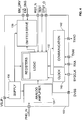
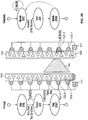
- FIG. 1 a schematic representation of a light curtain comprising two optical units is shown.
- the light curtain 100 in this embodiment consists of two identical first and second optical units 102, 104, which form between each other a plurality of light barriers for monitoring a protective field.
- the optical units 102, 104 may for instance be formed according to the principles of the European patent application EP 2511737 A1 , and may in particular use plug-in modules 106, 108 for defining their respective functionality.
- each optical unit 102, 104 comprises two identical modules 110 each having light emitting and light receiving elements. These optical modules 110 are identically built for both optical units 102, 104. Each of the optical units 102, 104 further comprises at least one second optical module 112 that also comprises a microcontroller providing the necessary intelligence to the optical unit 102, 104. Each of the modules 110, 112 may for instance have a height of about 150 mm. However, any other size or number of modules within each optical unit 102, 104 can also be used together with the present invention. Essentially, the first and second optical unit 102, 104 are identically built except for the plug-in modules 106a, 106b and 108a, 108b which are defining the particular functionality of each of the optical units.
- Each of the optical modules 110 comprises a plurality of optoelectronic components with their associated circuitry for emitting and sensing the radiation beams.
- the second optical module 112 contains the same optical functions and additionally, at least one microcontroller and optionally electronic circuitry, such as an interface with an external connector.
- the optoelectronic components do not necessarily have to be grouped in optical modules 110, 112.
- the light curtain may be formed by a linear array of radiation beams 114 which can either be infrared radiation with a wavelength between about 750 nm and 1000 nm, or visible light having a wavelength between about 620 nm and 800 nm.
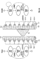
- the radiation beams 114 may for instance be activated sequentially, one beam at a time, from one peripheral end to the other peripheral end of each stick. Because each optical unit 102, 104 has transmitting and sensing photo elements, the scan through the light curtain activates every element sequentially and with an alternating direction, the beam being sent from the second optical unit 104 to the first optical unit 102 and back again. During such a scan sequence, the respective receiving stick always only sequentially detects the light from the pre-determined emitting element to the corresponding receiving element.
- each optical unit 102, 104 is formed by a plurality of optoelectronic components 116 each comprising at least one light-emitting element 118 and at least one light-receiving element 120.
- Each of the optoelectronic components 116 has a rather high degree of integrated intelligence in the form of a separate control element 122 which may for instance be formed as an integrated circuit, such as an application specific integrated circuit (ASIC).
- ASIC application specific integrated circuit
- Each of the optoelectronic components 116 provides electronic circuitry for driving the at least one light-emitting element 118 and for processing signals generated by the at least one light-receiving element 120.
- each of the optoelectronic components 116 is connected to a communication bus 124.
- a synchronization scheme is provided which is needed for accurately performing the complex emitting and detecting sequences performed by the light curtain of figures 1 and 2 .
- FIG. 3 shows in a schematic representation one optoelectronic component 116 with its interconnection terminals and the control element 122.
- the optoelectronic component 116 comprises a light emitting element, in particular a light emitting diode, LED, D2, and a light receiving element, in particular photo diode D1.
- the control element 122 is connected via a communication bus 124 to the next following optoelectronic component or, in case that it is the one next to the controller of the optical unit, to the controller.
- the bus comprises a data-out line which transports signals from the microcontroller (the master of the system) to the control element 122.
- the microcontroller the master of the system
- the communication bus 124 between the microcontroller functioning as the master and the plurality of control elements 122 is a serial/parallel bus based on three communication lines: a clock, a data-in line and a data-out line.
- the global system clock 126 is controlled by the master. This clock is recovered on each control element 122 and provides the main clock for the functioning of the control element 122.
- the data transmission line (data-out) is configured as a single bit unidirectional connection from the master to the control elements 122.
- the data-out line is a shared communication line out of the microcontroller to all of the control elements 122.
- all control elements 122 are connected in parallel and the transmission line is buffered on each module if the plurality of optoelectronic components is grouped together in optical modules 110.
- the data-in line 130 is another single bit unidirectional line for receiving data which is sent from the control elements 122 to the master.
- the data-in line 130 is a daisy chain line which is passed on from one control element 122 to the next.
- the control element receives data from the neighboring control element.
- An arrow gives the signal flow for this operation.
- the data are propagated to the next control element 122.
- every communication is initiated by the master.
- a particular control element 122 may only transmit information onto the data-in line 130 after a request originated by the master has been recognized and validated. The response onto the data-in line 130 must then follow the particular bus protocol.
- the communication line from the control elements 122 to the microcontroller is a point-to-point communication bus which is synchronous to the single global system clock. That means that each control element 122 takes information from the previous control element and forwards the merged results of that data and its internal data to the next control element, with a configurable option to register the data in a flip flop and send it on the following clock.
- Each control element 122 is connected to a single power line (V+) which may for instance be a 12 V to 15 V power line.
- the control element 122 may also comprise internal power management blocks for regulating its own power supply.
- the main functions of the optoelectronic component 116 lie in sensing and emitting pulsed radiation in a controlled manner under the supervision of a microcontroller.
- the photodiode D1 senses radiation, and in particular light, coming from the opposing optical unit and generates an analog input signal which is connected to a receiving amplifier integrated into the control element 122.
- a receiving amplifier integrated into the control element 122.
- control element 122 controls an LED drive circuit so that the LED D2 emits a radiation beam to the opposing optical unit.
- the drive circuit is controlled by the control element 122 in a way that the emitted light intensity has a specified level.
- more than one light-emitting diode D2 may be provided in the circuit according to FIG. 3 .
- the control element 122 is operable to communicate with the microcontroller over two communication lines.
- the communication line from the microcontroller to the control element 122 is a shared communication. All control elements in one module are connected in parallel with a digital buffer isolating each of the modules from the next one.
- an optical module 110 has eight optoelectronic components 116, forming a total of 16 beams, eight in each direction.
- a sensing input is provided for sensing the emitted current of the light emitting diode D2.
- FIG. 4 shows a schematic block diagram of the control element 122 according to FIG. 3 .
- the control element 122 may be formed by an integrated circuit and may in particular be realized in the form of an application specific integrated circuit, an ASIC, or a field programmable gate array design (FPGA).
- ASICs have the advantage of a full-custom capability, lower unit costs and a small form factor
- FPGAs have the advantage of a faster time to market and a simpler design cycle.
- the control element will often be called "ASIC". However, this does not restrict the control elements only to ASICs.
- the control element 112 has analog and digital sections as well as interfacing cells.
- the analog amplifier 134 is operable to detect the signals measured by the photodiode.
- the logic section 132 contains the registers which are used for storing the address of the particular control element 122.
- the clock 140 is used to synchronize all control elements with the microcontroller, run the internal logic, and sample the communication bus starter lines.
- the internal LED control 138 controls the LED current value by measuring the voltage across the external resistor R1 shown in FIG. 3 .
- the power supply block 136 generates the voltage for supplying the internal circuitry, such as the digital logic supply and the analog supply. Auxiliary voltages for the bias of the photodiode and the analog ground reference may also be generated here.
- the communication block 142 interfaces on one side with the external microcontroller serial bus 124, as shown in FIG. 3 , and on the other side with the internal logic 132.
- the communication interface 142 works with the frequency f RECCLK .
- the recovered clock signal is also input for a prescaler 146.
- This prescaler 146 is operable to generate a divided internal clock frequency having half, a quarter, or an eighth part of the recovered clock frequency.
- the prescaler 146 can also be set to leave the frequency undivided.
- the prescaler output frequency f PSCCLK is dependent on the prescaler configuration.
- the pulse pattern recognition, the timing measurements and so on are computed proportional to the divided clock frequency f PSCCLK , which according to an advantageous embodiment is half of the recovered clock frequency f RECCLK .
- the prescaler frequency would be between 0.4 and 2.4 MHz.
- other values can of course also be implemented.
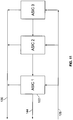
- FIG. 6 the communication between a particular optical module 110 and the controller module 112 is illustrated.
- the particular embodiment of using an ASIC as the control element 122 is considered.
- any other suitable technique for realizing a control element 122 can be employed here as well.
- each ASIC is assigned a unique identifying address which is stored in a bank of registers, and the ASICs respond to system commands via a shared serial bus. In response to the commands, the ASIC replies via a shared single-bit serial bus with an arbitration mechanism.
- the plurality of ASICs is interconnected by means of at least one serial daisy chain line which in the embodiment shown in FIG. 3 and 6 is provided by the data-in bus communication line 130.
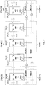
- FIG. 7 shows the case where a plurality of optical modules 110 is provided instead of the single optical module shown in FIG. 6 .
- the principles of the present invention may of course be employed for the embodiment shown in FIGs. 7 in the same way as for a case where only one module 110 is present.
- FIG. 8 essentially summarizes the bus topology used for the arrangement of FIG. 7 .
- the data-out line 128 connects to ASICs 122 in parallel, whereas the data-in line 130 which is directed towards the controller is a serial connection leading through all the ASICs 122.
- the arrangement according to FIG. 9 could be chosen, where both directions of the data transfer are leading through the ASICs 122 in series.
- the ASICs 122 can also be connected to each other in the form of a single-direction daisy chain which essentially represents a ring structured bus topology, as this is depicted in Figure 10 .
- At least one serial connection is advantageous for assigning individual addresses to each of the ASICs 122.
- the serial connection does not necessarily have to be one of the data lines 128 or 130, but may also be realized in the form of an additional enable line 144 used only for the address distribution.
- FIG. 11 shows a topology where the data-out line 128 is in parallel as well as the data-in line 130 and wherein an additional daisy chain 144 connects the ASIC 122 in series.
- emitted light pulses are expected within a particular time window.
- FIG. 12 illustrates a particular pulse pattern which may for instance be used for a scan or sensing procedure.
- the emitted radiation according to the present invention has the structure of a particular pulse pattern and there are different patterns which can be used to distinguish between normal scan pulses during the regular scan operation and a synchronization pattern that is only used for synchronizing the two optical units with respect to each other.
- different pulse patterns can for instance be used for a start signal, an acknowledge signal or the like.
- the pulse patterns emitted by the optoelectronic components can also have a specific coding depending on the particular optical units which the optoelectronic components belong to. This is an efficient way of eliminating disturbances due to other light curtains which are mounted in the direct vicinity.
- the pattern in the particular embodiment of FIG. 12 is formed by three pulses with two different time distances which are expected within a particular time window, indicated by the sensing phase.
- FIG. 12 gives the particular tolerances that have to be observed for correctly detecting these pulses.
- two further windows 148 and 150 can be defined for measuring a second and third pulse from the opposing optical unit.
- the timing information on when the pulses have been received can be determined and stored by the respective receiving control element 122.
- any other suitable pulse patterns can also be employed if needed.
- any desired number and type of signals can be encoded with a particular pulse pattern.
- t R_adjustSC can be used as a time stamp information 152 on when the pulse pattern has been sensed within the sensing window.
- the time span t HL defines a maximum allowable pulse width which is necessary for ensuring that the correct pulse pattern has been detected.
- the time stamp information 152 can be used for synchronizing further operations of the optical unit having received these signals.
- the times t R_P12SC and t R_P13SC define the distance between the first and second or third pulse respectively. They can be set individually before taking the light curtain into operation. Any other suitable beam coding may of course also be used.
- the receiving control element 122 After having received a particular pulse pattern within the sensing phase, the receiving control element 122 in general has at least two pieces of information which can be extracted from the sensing procedure: Firstly, the result of the pattern recognition as such leads to a status information. For instance, the particular pulse pattern shown in FIG. 12 may contain the information that a synchronization step is now to be performed. Secondly, the time stamp information 152 contains the information about the timing of the emitting optoelectronic component with respect to the internal timing of the particular detecting optoelectronic component.
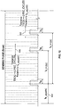
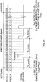
- FIG. 13 shows a timing diagram of the emitting phase for the case that a synchronization pulse pattern is to be emitted.
- FIG. 13 also shows the two clock frequencies of the recovered clock RECCLK and the prescaler clock PSCCLK which has half the frequency compared to the system clock.
- the pulse width of the emitted light pulses may for instance be defined by two rising edges of the recovered clock for a high signal. Of course, also broader pulses can be used.
- FIG. 14 shows the timing diagram for the corresponding sensing element.
- the sensing phase has a duration of t R_windowSC which typically amounts to 32 prescaler cycles.
- t R_windowSC typically amounts to 32 prescaler cycles.
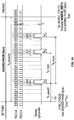
- FIG. 15 shows an example of the earliest correct light beam pattern that may be sensed.
- reference numeral 154 signifies the actual incident light pulses
- reference numeral 156 signifies an expected light pulse pattern which is generated upon detection of a light pulse at the beginning of the sensing window.
- FIG. 17 shows the latest possible arrival of the pulse pattern for detecting a complete pattern within the time frame of the receiving window.
- the time stamp information 152 is determined by the time difference between the beginning the receiving window and the detection of the first pulse.
- the time stamp information 152 can be derived from this measurement and a respective synchronization can be performed accordingly.
- FIG. 19 illustrates the case where the first pulse is missing and only the second and third pulses are detected within the sensing timeframe. In such a situation, not a simple synchronization signal is sent to the controller, but an error message can be output. The same is valid for the cases where either the second or third pulse is missing as depicted in FIGs. 20 and 21 .
- FIG 22 Another case where not a simple time adjustment is performed but where an error is registered, is shown in FIG 22 , where an additional pulse as shown in FIG. 22 , an additional fourth pulse is detected and moreover the complete pattern, and in particular the time between the first and second pulse, do not coincide with the expected values. Hence, again an error message is generated.
- a particular optoelectronic component Upon receiving a SYNC command from the controller 111, a particular optoelectronic component emits in a predefined emitting phase the pulse pattern as shown in FIG. 23 .
- the particular times are given in the parameters of the registers.
- the opposing optical unit samples the emitted synchronization pulse pattern ideally within its sensing phase window, as shown in FIG. 24 .
- the different measured timing values are used for recognizing whether a correct pattern has been received as illustrated before.
- the time stamp information 152 can be used for performing an adjustment between the timings of the first and second optical unit in order to synchronize same. As explained before, this is, of course, only done in case that the correct synchronization pattern is detected somewhere within the sensing window.
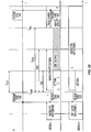
- the timing and signal flow within one optical unit for the synchronization will be explained in the following, with reference to FIG. 25 .
- the timing of the signals of the microcontroller is shown when interacting with two particular ASICs. One, for which the command is intended (ASIC# m.n) and another one for which the command is not intended (ASIC# m.n+1).
- the microcontroller sends a SYNC command on the bus which is received by all ASICs connected to the bus.
- the ASICs are all in a mode where they are waiting for a new command, as indicated by FIG. 25 . They all receive the SYNC command, but only the ASIC that is intended to send a synchronization signal to the opposing optical unit reacts to this command.
- the ASIC# m.n+1 stays in the waiting status after the settling time, whereas the active ASIC# m.n enters an emitting phase after the settling phase has passed.
- the ASIC# m.n sends an answer to the bus master ⁇ C after a further specified delay time and is then ready for a new command.
- an individual address which is unique for each ASIC is provided and leads to the distinction whether the receiving ASIC decodes the particular SYNC command and acts accordingly or just waits for a new command on the bus.
- FIG. 26 deals with the signalling on the sensing side where a SYNC command initiates the sensing phase.
- the ASIC# m.n and ASIC# m.n+1 both receive a synchronization signal 158 from the opposing optical unit.
- a synchronization pulse 158 is detected, a synchronization answer is transmitted to the microcontroller.
- This particular synchronization answer contains the information whether a correct pulse pattern has been received and what time stamp information has been measured.
- no synchronization answer is transmitted back to the microcontroller.
- the synchronization subcommand for sensing synchronization pulses can be transmitted from the microcontroller in a broadcast variant so that all ASICs can execute the command.
- the synchronization subcommand for sensing synchronization pulses can be transmitted from the microcontroller in a broadcast variant so that all ASICs can execute the command.
- a direct address method is used, only the ASIC which has a matching address will execute the command. If the address does not match, the ASIC waits for the next command.
- FIG. 26 further shows that the delay times T DELAY_COUNTER for the different ASICs are different and that in particular the ASIC with a higher priority, here the ASIC which is located further away from the microcontroller, will win the arbitration phase.
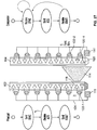
- FIGs. 27 to 30 illustrate a synchronization procedure according to the present invention between a first and a second optical unit 102 and 104.
- the optical unit 102 is defined as the principal optical unit (master) and the optical unit 104 has the function of a companion (slave).
- This step is illustrated in FIG. 28 .
- the optical radiation is not only sent towards one receiving element but to more than one receiving elements which means that in total three optoelectronic elements receive an acknowledge signal.
- the belonging ASICs 122-1, 122-2 and 122-3 send a respective message to their controller 111.
- the arbitration phase is won by the optoelectronic element which is distanced the furthest from the controller 111.
- the principal optical unit 102 repeats the sending of the synchronization signal several times in case that after a pre-determined time no acknowledge signal is received. Then the same procedure starts with the next following optoelectronic element until an acknowledge pulse is received.
- the acknowledge signal arrives at the principal optical unit 102, the time of the receipt is measured and a start pulse within a well-defined time window is emitted towards the companion optical unit 104.
- FIG. 29 This is illustrated in FIG. 29 .
- the controller 111 of the principal optical unit 102 may instruct any other ASIC 122 to transmit the start pulse, it is advantageous to use one of those optoelectronic elements which have already proven that an uninterrupted light path can be established towards a companion optical unit 104.
- the measurements have shown that between the optoelectronic element 116-3 the principal optical unit 102 and the optoelectronic element 116'-2 of the companion optical unit 104, there exists an undisturbed optical path between the two optical units which for the future operation may be used for resynchronizing the two sticks if necessary.
- the start pulse which is a pattern that is received by the companion optical unit 104 directly triggers the normal scan operation which therefore is directly synchronized with the principle optical unit 102.
- FIG. 31 summarizes this synchronization scheme in the form of a timing diagram for the two optical units 102 and 104 for the example of four involved ASICs.
- the microcontroller is the bus master in each stick.
- the bus master of the companion optical unit 104 transmits the broadcasting command to put all receiving elements into a receiving state where it is waiting for a synchronization pattern.
- ASIC # n is instructed by the bus master of the principle optical unit to emit a synchronization pattern. After having emitted the synchronization pattern, the ASIC # n informs the bus master via an answer message that the sending has been performed and the bus master subsequently instructs all ASICs to switch into a receiving mode so that an incident acknowledge signal will be detected.
- One or more of the ASICs of the companion receive within their receiving window the synchronization pulse and they all answer back to the bus master.
- the ASIC n Due to the arbitration phase only the one which is having the highest priority, here the ASIC n, is instructed to transmit an acknowledge pulse back to the principle optical unit. As here all the optoelectronic elements are enabled to receive the acknowledge pattern from the companion side, all of them send back an answer to their principle bus master. Again the ASIC with the highest priority is instructed to emit a start pulse which according to an advantageous embodiment is received only by the particular optoelectronic element which has emitted the acknowledge pattern. This leads to the most accurate results. Upon receipt of the start pattern, the ASIC n of the companion optical unit transmits an answer to its bus master which leads to a start of the normal scan operation. Further, the two optical units now know a free beam pair which can also be used to interchange data and in any case they both simultaneously know the moment when the sequential scan through the light curtain for a normal san operation has to start.
- Reference Numeral Description 100 light curtain 102 first optical unit 104 second optical unit 106 first plug-in module 108 second plug-in module 110 first optical module (without controller) 111, 111' controller 112 second optical module (with controller), controller module 114 radiation beam 116 optoelectronic component 118 light emitting element 120 light receiving element 122, 122' control element/ASIC 124 communication bus 126 system clock 128 data-out 130 data-in 132 internal logic 134 amplifier 136 supply 138 emitter drive 140 clock 141 clock restoration 142 communication 144 daisy chain 146 prescaler 148 time window for second pulse 150 time window for third pulse 152 time stamp information 154 incident pulses 156 expected pulses
Landscapes
- Physics & Mathematics (AREA)
- Life Sciences & Earth Sciences (AREA)
- General Life Sciences & Earth Sciences (AREA)
- General Physics & Mathematics (AREA)
- Geophysics (AREA)
- Optical Communication System (AREA)
Claims (16)
- Verfahren zur Synchronisierung mindestens zweier optischer Einheiten einer Lichtschranke, wobei die Schranke einen Überwachungsbereich überwacht und mindestens eine erste optische Einheit und mindestens eine zweite optische Einheit aufweist, wobei jede optische Einheit mehrere optoelektronische Komponenten mit mindestens einem optischen Sender, mindestens einem optischen Empfänger und mindestens einem Steuerelement aufweist, wobei das Verfahren die Schritte umfasst:Aussenden einer Strahlung, die ein Synchronisierungssignal bildet, aus einem ersten optischen Sender der ersten optischen Einheit derart, dass die Strahlung mindestens zwei optische Empfänger auf der gegenüberliegenden Seite erreicht,Steuern mehrerer der optischen Empfänger der mindestens einen zweiten optischen Einheit derart, dass überwacht wird, ob das Synchronisierungssignal empfangen worden ist, und Ausführen eines Synchronisierungsschritts, wenn das Synchronisierungssignal empfangen worden ist;wobei das Verfahren ferner den Schritt ausführt: Bestimmen mindestens einer der mehreren optoelektronischen Komponenten, die für den Synchronisierungsschritt zu verwenden ist.
- Verfahren nach Anspruch 1, wobei eine Zeitinformation darüber gespeichert wird, wann das Synchronisierungssignal erkannt worden ist, wenn das Synchronisierungssignal erkannt wird.
- Verfahren nach Anspruch 2, wobei das Synchronisierungssignal innerhalb eines vordefinierten Zeitfensters in der zweiten optischen Einheit erwartet wird, und wobei die Position des erkannten Signals innerhalb des Zeitfensters als ein Zeitstempel zur Bereitstellung der Zeitinformation gespeichert wird.
- Verfahren nach einem der Ansprüche 1 bis 3, wobei die optischen Sender der mehreren zweiten optischen Einheiten so gesteuert werden, dass sie Strahlung zur Bildung eines Bestätigungssignals aussenden, wenn das Synchronisierungssignal erkannt wird.
- Verfahren nach Anspruch 4, wobei ein Startsignal aus einem ersten optischen Sender der ersten optischen Einheit zum Starten eines Überwachungsvorgangs bei Empfang des Bestätigungssignals gesendet wird.
- Verfahren nach Anspruch 5, wobei das Synchronisierungssignal und/oder das Bestätigungssignal und/oder das Startsignal ein gepulstes Signal sind, das ein spezielles Pulsmuster hat.
- Verfahren nach einem der Ansprüche 4 bis 6, wobei, wenn kein Bestätigungssignal nach dem Schritt des Sendens des Synchronisierungssignals aus einem ersten optischen Sender der ersten optischen Einheit erkannt wird, das Aussenden des Synchronisierungssignals aus einem zweiten optischen Sender der ersten optischen Einheit wiederholt wird.
- Verfahren nach einem der Ansprüche 4 bis 7, wobei das Synchronisierungssignal von jeder der mehreren optoelektronischen Komponenten der Reihe nach ausgesendet wird, bis ein Bestätigungssignal erkannt wird oder ein vordefinierter Zeitüberlauf erreicht wird.
- Verfahren nach einem der vorhergehenden Ansprüche, wobei mehrere der optoelektronischen Komponenten einer optischen Einheit gleichzeitig überwachen, ob das Synchronisierungssignal empfangen wird.
- Verfahren nach einem der vorhergehenden Ansprüche, wobei mehrere optische Einheiten miteinander synchronisiert werden.
- Verfahren nach einem der vorhergehenden Ansprüche, wobei jede optoelektronische Komponente für den Synchronisierungsvorgang verwendbar ist.
- Verfahren nach einem der vorhergehenden Ansprüche, wobei jede optische Einheit ein Steuermodul aufweist, wobei die Steuerelemente der optoelektronischen Komponenten untereinander und mit dem Steuermodul über einen Kommunikationsbus verbunden sind, und wobei die Synchronisierung durch einen Synchronisierungsbefehl, der von dem Steuermodul ausgesendet wird, in Gang gesetzt wird.
- Verfahren nach Anspruch 12, wobei ein Zugriff auf den Kommunikationsbus durch ein Buszugriffsschema gesteuert wird, das sicherstellt, dass nur die optoelektronische Komponente mit der höchsten Priorität Daten über den Kommunikationsbus sendet, vorzugsweise durch ein Trägererfassungs-Mehrfach-Zugriffs/Kollisions-Vermeidungs- (CSMA/CA) Zugriffsschema.
- Lichtschranke zur Überwachung eines Überwachungsbereichs, wobei die Schranke mindestens eine erste optische Einheit (102) und mindestens eine zweite optische Einheit (104) aufweist, wobei jede optische Einheit mehrere optoelektronische Komponenten mit mindestens einem optischen Sender, mindestens einem optischen Empfänger und mindestens einem Steuerelement aufweist,
wobei die erste und die zweite optische Einheit ausgebildet sind, durch Ausführen eines Verfahrens nach einem der vorhergehenden Ansprüche synchronisiert zu werden. - Lichtschranke nach Anspruch 14, wobei die Steuerelemente (122) der optoelektronischen Komponenten über einen Kommunikationsbus (124) miteinander verbunden sind.
- Lichtschranke nach Anspruch 14 oder 15, wobei mindestens eine der optischen Einheiten ein Steuermodul (112) zur Steuerung des Betriebs der Steuerelemente aufweist, und/oder wobei mindestens eine der optischen Einheiten ein Schnittstellenelement zur elektrischen Verbindung der optischen Einheit mit einer externen elektrischen Schaltung aufweist.
Priority Applications (3)
| Application Number | Priority Date | Filing Date | Title |
|---|---|---|---|
| EP13171484.2A EP2813868B1 (de) | 2013-06-11 | 2013-06-11 | Verfahren zur Synchronisation optischer Einheiten einer Lichtschranke und Lichtvorhang |
| CN201410222318.4A CN104237962B (zh) | 2013-06-11 | 2014-05-23 | 用于使光电屏障的光学单元同步的方法以及光幕 |
| US14/301,436 US9798040B2 (en) | 2013-06-11 | 2014-06-11 | Method for synchronizing optical units of a photoelectric barrier and light curtain |
Applications Claiming Priority (1)
| Application Number | Priority Date | Filing Date | Title |
|---|---|---|---|
| EP13171484.2A EP2813868B1 (de) | 2013-06-11 | 2013-06-11 | Verfahren zur Synchronisation optischer Einheiten einer Lichtschranke und Lichtvorhang |
Publications (2)
| Publication Number | Publication Date |
|---|---|
| EP2813868A1 EP2813868A1 (de) | 2014-12-17 |
| EP2813868B1 true EP2813868B1 (de) | 2021-08-04 |
Family
ID=48626308
Family Applications (1)
| Application Number | Title | Priority Date | Filing Date |
|---|---|---|---|
| EP13171484.2A Active EP2813868B1 (de) | 2013-06-11 | 2013-06-11 | Verfahren zur Synchronisation optischer Einheiten einer Lichtschranke und Lichtvorhang |
Country Status (3)
| Country | Link |
|---|---|
| US (1) | US9798040B2 (de) |
| EP (1) | EP2813868B1 (de) |
| CN (1) | CN104237962B (de) |
Families Citing this family (10)
| Publication number | Priority date | Publication date | Assignee | Title |
|---|---|---|---|---|
| JP5874412B2 (ja) * | 2012-01-30 | 2016-03-02 | セイコーエプソン株式会社 | ロボット、進入検出方法 |
| CN105242326A (zh) * | 2015-09-02 | 2016-01-13 | 浙江工商大学 | 一种变频跟踪红外对射式人行通道通行目标检测方法 |
| EP3528014B1 (de) | 2018-02-16 | 2023-05-03 | Rockwell Automation Switzerland GmbH | Lichtvorhang und verfahren zum betrieb eines lichtvorhangs |
| CN109827609A (zh) * | 2019-02-22 | 2019-05-31 | 上海兰宝传感科技股份有限公司 | 高性能测量光幕系统 |
| DE102019118104B4 (de) * | 2019-07-04 | 2024-05-16 | Sick Ag | Optoelektronische Sensoranordnung |
| EP3822925B1 (de) * | 2019-11-13 | 2024-01-10 | Conduent Business Services, LLC | Optische detektion in zugangskontrollsystemen |
| US12050099B2 (en) * | 2020-02-21 | 2024-07-30 | The Boeing Company | Systems and methods for determining space availability in an aircraft |
| US10996051B1 (en) * | 2020-02-21 | 2021-05-04 | The Boeing Company | Systems and methods for determining space availability in an aircraft |
| WO2022080484A1 (ja) * | 2020-10-16 | 2022-04-21 | 株式会社島津製作所 | データ計測システムおよび計測データのデータ処理を実行する方法 |
| CN118529582B (zh) * | 2024-07-29 | 2024-11-22 | 伟龙意程智能科技(江苏)有限公司 | 一种电梯光幕节能控制方法及低功耗无线通信光幕 |
Family Cites Families (18)
| Publication number | Priority date | Publication date | Assignee | Title |
|---|---|---|---|---|
| SE456952B (sv) * | 1982-12-16 | 1988-11-14 | Innovationsteknik Inst Ab | Mikrodatorstyrd ljusridaa |
| US4650990A (en) * | 1984-08-16 | 1987-03-17 | Joensson Nils | Processor-controlled light screen wherein light beam carries coded signals |
| CH667340A5 (de) * | 1985-04-30 | 1988-09-30 | Cerberus Ag | Lichtschranke. |
| DE19510304C1 (de) * | 1995-03-22 | 1996-02-01 | Leuze Electronic Gmbh & Co | Lichtschrankengitter |
| FR2898716B1 (fr) | 2006-03-16 | 2008-12-26 | Rhodanienne D Electronique App | Barriere a infrarouge actif a cellules mixtes a la fois emettrices et receptrices |
| EP1870734B1 (de) | 2006-06-20 | 2009-01-14 | Sick Ag | Optoelektronisches Sicherheitslichtgitter mit wenigstens zwei Sende-Empfangsleisten |
| DE102007024210A1 (de) | 2007-05-15 | 2008-11-27 | Pilz Gmbh & Co. Kg | Optoelektronischer Sensor zum Absichern eines Gefahrenbereichs |
| DE102007059565B4 (de) * | 2007-12-11 | 2010-01-07 | Leuze Lumiflex Gmbh + Co. Kg | Lichtgitter und Verfahren zu dessen Betrieb |
| CN101655566B (zh) * | 2009-09-15 | 2013-02-20 | 江苏汉武智能科技有限公司 | 区域检测光幕及其检测方法 |
| CN201801283U (zh) * | 2009-12-31 | 2011-04-20 | 上海兰宝传感器有限公司 | 光幕传感器 |
| JP5465563B2 (ja) * | 2010-03-19 | 2014-04-09 | 株式会社キーエンス | 多光軸光電センサ |
| CN101811638B (zh) * | 2010-04-16 | 2012-10-17 | 杭州优迈科技有限公司 | 纵向式电梯光幕系统及纵向式电梯光幕探测方法 |
| DE102010037681B4 (de) * | 2010-09-21 | 2018-12-27 | Sick Ag | Lichtgitter und Verfahren zur Objektvermessung mit einem Lichtgitter |
| CN102069417B (zh) * | 2010-09-29 | 2013-06-26 | 惠州市大亚湾天马电子机械有限公司 | 线束交叉型安全光栅检测装置 |
| EP2511737B1 (de) | 2011-04-13 | 2021-09-15 | Rockwell Automation Switzerland GmbH | Modularer Lichtvorhang und Plug-in Modul dafür |
| CN102707330B (zh) * | 2012-06-11 | 2014-08-27 | 易程(苏州)电子科技股份有限公司 | 用于检票通道的监测方法 |
| ES2587227T3 (es) * | 2012-09-28 | 2016-10-21 | Sick Ag | Rejilla reticular y procedimiento para la vigilancia de una zona de vigilancia |
| CN203177889U (zh) * | 2013-03-29 | 2013-09-04 | 上海兰宝传感科技股份有限公司 | 一种区域光幕传感器 |
-
2013
- 2013-06-11 EP EP13171484.2A patent/EP2813868B1/de active Active
-
2014
- 2014-05-23 CN CN201410222318.4A patent/CN104237962B/zh active Active
- 2014-06-11 US US14/301,436 patent/US9798040B2/en active Active
Also Published As
| Publication number | Publication date |
|---|---|
| US20140361149A1 (en) | 2014-12-11 |
| EP2813868A1 (de) | 2014-12-17 |
| CN104237962A (zh) | 2014-12-24 |
| CN104237962B (zh) | 2017-07-28 |
| US9798040B2 (en) | 2017-10-24 |
Similar Documents
| Publication | Publication Date | Title |
|---|---|---|
| EP2813868B1 (de) | Verfahren zur Synchronisation optischer Einheiten einer Lichtschranke und Lichtvorhang | |
| EP2808706B1 (de) | Sender-Empfängerelement für eine optische Einheit einer Lichtschranke und fotoelektrischer Lichtvorhang | |
| US10113694B2 (en) | Time-of-flight safety photoelectric barrier and method of monitoring a protective field | |
| JPH11353986A (ja) | 複数エリアセンサ用制御器 | |
| EP2796903B1 (de) | Optische Einheit, Lichtvorhang und Verfahren zur Zuordnung einer individuellen Adresse | |
| US8058605B2 (en) | Optoelectronic sensor for safeguarding a hazardous area | |
| EP2730939B1 (de) | Sensorsystem | |
| EP2511737B1 (de) | Modularer Lichtvorhang und Plug-in Modul dafür | |
| CN100490324C (zh) | 多光轴光电传感器 | |
| US6411856B1 (en) | General operation integrated control method and its controller | |
| CN101811638A (zh) | 纵向式电梯光幕系统及纵向式电梯光幕探测方法 | |
| JP2011198595A (ja) | 多光軸光電センサ | |
| US5424532A (en) | Multi-beam light barrier with monitoring of malfunction | |
| CN105371094A (zh) | 多光轴光电传感器 | |
| JP2003057360A (ja) | 多光軸光電式安全装置 | |
| JP2013223237A (ja) | 多光軸光電センサ | |
| JP2003133933A (ja) | 多光軸光電センサ | |
| KR102237695B1 (ko) | 다광축 광전 센서 | |
| JPWO1995010789A1 (ja) | フェールセーフ多光軸光線式センサ | |
| JPH0772752B2 (ja) | 赤外線警戒装置 | |
| JP4079291B2 (ja) | 増設型多光軸光電スイッチ | |
| EP3528014B1 (de) | Lichtvorhang und verfahren zum betrieb eines lichtvorhangs | |
| JP2513335Y2 (ja) | 多光軸式光電スイッチ | |
| KR100960354B1 (ko) | 외란광 방지 빔 센서의 동작 방법 | |
| JPH07208690A (ja) | 工作機の光線式安全装置 |
Legal Events
| Date | Code | Title | Description |
|---|---|---|---|
| 17P | Request for examination filed |
Effective date: 20130611 |
|
| AK | Designated contracting states |
Kind code of ref document: A1 Designated state(s): AL AT BE BG CH CY CZ DE DK EE ES FI FR GB GR HR HU IE IS IT LI LT LU LV MC MK MT NL NO PL PT RO RS SE SI SK SM TR |
|
| AX | Request for extension of the european patent |
Extension state: BA ME |
|
| PUAI | Public reference made under article 153(3) epc to a published international application that has entered the european phase |
Free format text: ORIGINAL CODE: 0009012 |
|
| R17P | Request for examination filed (corrected) |
Effective date: 20150603 |
|
| RBV | Designated contracting states (corrected) |
Designated state(s): AL AT BE BG CH CY CZ DE DK EE ES FI FR GB GR HR HU IE IS IT LI LT LU LV MC MK MT NL NO PL PT RO RS SE SI SK SM TR |
|
| RAP1 | Party data changed (applicant data changed or rights of an application transferred) |
Owner name: ROCKWELL AUTOMATION SAFETY AG |
|
| RAP1 | Party data changed (applicant data changed or rights of an application transferred) |
Owner name: ROCKWELL AUTOMATION SWITZERLAND GMBH |
|
| GRAP | Despatch of communication of intention to grant a patent |
Free format text: ORIGINAL CODE: EPIDOSNIGR1 |
|
| STAA | Information on the status of an ep patent application or granted ep patent |
Free format text: STATUS: GRANT OF PATENT IS INTENDED |
|
| INTG | Intention to grant announced |
Effective date: 20210120 |
|
| GRAS | Grant fee paid |
Free format text: ORIGINAL CODE: EPIDOSNIGR3 |
|
| GRAA | (expected) grant |
Free format text: ORIGINAL CODE: 0009210 |
|
| STAA | Information on the status of an ep patent application or granted ep patent |
Free format text: STATUS: THE PATENT HAS BEEN GRANTED |
|
| AK | Designated contracting states |
Kind code of ref document: B1 Designated state(s): AL AT BE BG CH CY CZ DE DK EE ES FI FR GB GR HR HU IE IS IT LI LT LU LV MC MK MT NL NO PL PT RO RS SE SI SK SM TR |
|
| REG | Reference to a national code |
Ref country code: GB Ref legal event code: FG4D |
|
| REG | Reference to a national code |
Ref country code: AT Ref legal event code: REF Ref document number: 1417536 Country of ref document: AT Kind code of ref document: T Effective date: 20210815 |
|
| REG | Reference to a national code |
Ref country code: CH Ref legal event code: EP |
|
| REG | Reference to a national code |
Ref country code: DE Ref legal event code: R096 Ref document number: 602013078609 Country of ref document: DE |
|
| REG | Reference to a national code |
Ref country code: IE Ref legal event code: FG4D |
|
| REG | Reference to a national code |
Ref country code: LT Ref legal event code: MG9D |
|
| REG | Reference to a national code |
Ref country code: NL Ref legal event code: MP Effective date: 20210804 |
|
| REG | Reference to a national code |
Ref country code: AT Ref legal event code: MK05 Ref document number: 1417536 Country of ref document: AT Kind code of ref document: T Effective date: 20210804 |
|
| PG25 | Lapsed in a contracting state [announced via postgrant information from national office to epo] |
Ref country code: SE Free format text: LAPSE BECAUSE OF FAILURE TO SUBMIT A TRANSLATION OF THE DESCRIPTION OR TO PAY THE FEE WITHIN THE PRESCRIBED TIME-LIMIT Effective date: 20210804 Ref country code: HR Free format text: LAPSE BECAUSE OF FAILURE TO SUBMIT A TRANSLATION OF THE DESCRIPTION OR TO PAY THE FEE WITHIN THE PRESCRIBED TIME-LIMIT Effective date: 20210804 Ref country code: RS Free format text: LAPSE BECAUSE OF FAILURE TO SUBMIT A TRANSLATION OF THE DESCRIPTION OR TO PAY THE FEE WITHIN THE PRESCRIBED TIME-LIMIT Effective date: 20210804 Ref country code: NO Free format text: LAPSE BECAUSE OF FAILURE TO SUBMIT A TRANSLATION OF THE DESCRIPTION OR TO PAY THE FEE WITHIN THE PRESCRIBED TIME-LIMIT Effective date: 20211104 Ref country code: PT Free format text: LAPSE BECAUSE OF FAILURE TO SUBMIT A TRANSLATION OF THE DESCRIPTION OR TO PAY THE FEE WITHIN THE PRESCRIBED TIME-LIMIT Effective date: 20211206 Ref country code: ES Free format text: LAPSE BECAUSE OF FAILURE TO SUBMIT A TRANSLATION OF THE DESCRIPTION OR TO PAY THE FEE WITHIN THE PRESCRIBED TIME-LIMIT Effective date: 20210804 Ref country code: FI Free format text: LAPSE BECAUSE OF FAILURE TO SUBMIT A TRANSLATION OF THE DESCRIPTION OR TO PAY THE FEE WITHIN THE PRESCRIBED TIME-LIMIT Effective date: 20210804 Ref country code: BG Free format text: LAPSE BECAUSE OF FAILURE TO SUBMIT A TRANSLATION OF THE DESCRIPTION OR TO PAY THE FEE WITHIN THE PRESCRIBED TIME-LIMIT Effective date: 20211104 Ref country code: AT Free format text: LAPSE BECAUSE OF FAILURE TO SUBMIT A TRANSLATION OF THE DESCRIPTION OR TO PAY THE FEE WITHIN THE PRESCRIBED TIME-LIMIT Effective date: 20210804 Ref country code: LT Free format text: LAPSE BECAUSE OF FAILURE TO SUBMIT A TRANSLATION OF THE DESCRIPTION OR TO PAY THE FEE WITHIN THE PRESCRIBED TIME-LIMIT Effective date: 20210804 |
|
| PG25 | Lapsed in a contracting state [announced via postgrant information from national office to epo] |
Ref country code: PL Free format text: LAPSE BECAUSE OF FAILURE TO SUBMIT A TRANSLATION OF THE DESCRIPTION OR TO PAY THE FEE WITHIN THE PRESCRIBED TIME-LIMIT Effective date: 20210804 Ref country code: LV Free format text: LAPSE BECAUSE OF FAILURE TO SUBMIT A TRANSLATION OF THE DESCRIPTION OR TO PAY THE FEE WITHIN THE PRESCRIBED TIME-LIMIT Effective date: 20210804 Ref country code: GR Free format text: LAPSE BECAUSE OF FAILURE TO SUBMIT A TRANSLATION OF THE DESCRIPTION OR TO PAY THE FEE WITHIN THE PRESCRIBED TIME-LIMIT Effective date: 20211105 |
|
| PG25 | Lapsed in a contracting state [announced via postgrant information from national office to epo] |
Ref country code: NL Free format text: LAPSE BECAUSE OF FAILURE TO SUBMIT A TRANSLATION OF THE DESCRIPTION OR TO PAY THE FEE WITHIN THE PRESCRIBED TIME-LIMIT Effective date: 20210804 |
|
| PG25 | Lapsed in a contracting state [announced via postgrant information from national office to epo] |
Ref country code: DK Free format text: LAPSE BECAUSE OF FAILURE TO SUBMIT A TRANSLATION OF THE DESCRIPTION OR TO PAY THE FEE WITHIN THE PRESCRIBED TIME-LIMIT Effective date: 20210804 |
|
| REG | Reference to a national code |
Ref country code: DE Ref legal event code: R097 Ref document number: 602013078609 Country of ref document: DE |
|
| PG25 | Lapsed in a contracting state [announced via postgrant information from national office to epo] |
Ref country code: SM Free format text: LAPSE BECAUSE OF FAILURE TO SUBMIT A TRANSLATION OF THE DESCRIPTION OR TO PAY THE FEE WITHIN THE PRESCRIBED TIME-LIMIT Effective date: 20210804 Ref country code: SK Free format text: LAPSE BECAUSE OF FAILURE TO SUBMIT A TRANSLATION OF THE DESCRIPTION OR TO PAY THE FEE WITHIN THE PRESCRIBED TIME-LIMIT Effective date: 20210804 Ref country code: RO Free format text: LAPSE BECAUSE OF FAILURE TO SUBMIT A TRANSLATION OF THE DESCRIPTION OR TO PAY THE FEE WITHIN THE PRESCRIBED TIME-LIMIT Effective date: 20210804 Ref country code: EE Free format text: LAPSE BECAUSE OF FAILURE TO SUBMIT A TRANSLATION OF THE DESCRIPTION OR TO PAY THE FEE WITHIN THE PRESCRIBED TIME-LIMIT Effective date: 20210804 Ref country code: CZ Free format text: LAPSE BECAUSE OF FAILURE TO SUBMIT A TRANSLATION OF THE DESCRIPTION OR TO PAY THE FEE WITHIN THE PRESCRIBED TIME-LIMIT Effective date: 20210804 Ref country code: AL Free format text: LAPSE BECAUSE OF FAILURE TO SUBMIT A TRANSLATION OF THE DESCRIPTION OR TO PAY THE FEE WITHIN THE PRESCRIBED TIME-LIMIT Effective date: 20210804 |
|
| PLBE | No opposition filed within time limit |
Free format text: ORIGINAL CODE: 0009261 |
|
| STAA | Information on the status of an ep patent application or granted ep patent |
Free format text: STATUS: NO OPPOSITION FILED WITHIN TIME LIMIT |
|
| 26N | No opposition filed |
Effective date: 20220506 |
|
| PG25 | Lapsed in a contracting state [announced via postgrant information from national office to epo] |
Ref country code: IT Free format text: LAPSE BECAUSE OF FAILURE TO SUBMIT A TRANSLATION OF THE DESCRIPTION OR TO PAY THE FEE WITHIN THE PRESCRIBED TIME-LIMIT Effective date: 20210804 |
|
| PG25 | Lapsed in a contracting state [announced via postgrant information from national office to epo] |
Ref country code: SI Free format text: LAPSE BECAUSE OF FAILURE TO SUBMIT A TRANSLATION OF THE DESCRIPTION OR TO PAY THE FEE WITHIN THE PRESCRIBED TIME-LIMIT Effective date: 20210804 |
|
| PG25 | Lapsed in a contracting state [announced via postgrant information from national office to epo] |
Ref country code: MC Free format text: LAPSE BECAUSE OF FAILURE TO SUBMIT A TRANSLATION OF THE DESCRIPTION OR TO PAY THE FEE WITHIN THE PRESCRIBED TIME-LIMIT Effective date: 20210804 |
|
| REG | Reference to a national code |
Ref country code: CH Ref legal event code: PL |
|
| REG | Reference to a national code |
Ref country code: BE Ref legal event code: MM Effective date: 20220630 |
|
| PG25 | Lapsed in a contracting state [announced via postgrant information from national office to epo] |
Ref country code: LU Free format text: LAPSE BECAUSE OF NON-PAYMENT OF DUE FEES Effective date: 20220611 Ref country code: LI Free format text: LAPSE BECAUSE OF NON-PAYMENT OF DUE FEES Effective date: 20220630 Ref country code: IE Free format text: LAPSE BECAUSE OF NON-PAYMENT OF DUE FEES Effective date: 20220611 Ref country code: CH Free format text: LAPSE BECAUSE OF NON-PAYMENT OF DUE FEES Effective date: 20220630 |
|
| PG25 | Lapsed in a contracting state [announced via postgrant information from national office to epo] |
Ref country code: BE Free format text: LAPSE BECAUSE OF NON-PAYMENT OF DUE FEES Effective date: 20220630 |
|
| P01 | Opt-out of the competence of the unified patent court (upc) registered |
Effective date: 20230404 |
|
| PG25 | Lapsed in a contracting state [announced via postgrant information from national office to epo] |
Ref country code: HU Free format text: LAPSE BECAUSE OF FAILURE TO SUBMIT A TRANSLATION OF THE DESCRIPTION OR TO PAY THE FEE WITHIN THE PRESCRIBED TIME-LIMIT; INVALID AB INITIO Effective date: 20130611 |
|
| PG25 | Lapsed in a contracting state [announced via postgrant information from national office to epo] |
Ref country code: MK Free format text: LAPSE BECAUSE OF FAILURE TO SUBMIT A TRANSLATION OF THE DESCRIPTION OR TO PAY THE FEE WITHIN THE PRESCRIBED TIME-LIMIT Effective date: 20210804 Ref country code: CY Free format text: LAPSE BECAUSE OF FAILURE TO SUBMIT A TRANSLATION OF THE DESCRIPTION OR TO PAY THE FEE WITHIN THE PRESCRIBED TIME-LIMIT Effective date: 20210804 |
|
| PG25 | Lapsed in a contracting state [announced via postgrant information from national office to epo] |
Ref country code: MT Free format text: LAPSE BECAUSE OF FAILURE TO SUBMIT A TRANSLATION OF THE DESCRIPTION OR TO PAY THE FEE WITHIN THE PRESCRIBED TIME-LIMIT Effective date: 20210804 |
|
| PGFP | Annual fee paid to national office [announced via postgrant information from national office to epo] |
Ref country code: DE Payment date: 20250520 Year of fee payment: 13 |
|
| PGFP | Annual fee paid to national office [announced via postgrant information from national office to epo] |
Ref country code: GB Payment date: 20250520 Year of fee payment: 13 |
|
| PGFP | Annual fee paid to national office [announced via postgrant information from national office to epo] |
Ref country code: FR Payment date: 20250520 Year of fee payment: 13 |