EP2797231B1 - Unterschiedliche Differenzschaltung - Google Patents
Unterschiedliche Differenzschaltung Download PDFInfo
- Publication number
- EP2797231B1 EP2797231B1 EP14165501.9A EP14165501A EP2797231B1 EP 2797231 B1 EP2797231 B1 EP 2797231B1 EP 14165501 A EP14165501 A EP 14165501A EP 2797231 B1 EP2797231 B1 EP 2797231B1
- Authority
- EP
- European Patent Office
- Prior art keywords
- transistor
- differential
- bulk
- coupled
- offset voltage
- Prior art date
- Legal status (The legal status is an assumption and is not a legal conclusion. Google has not performed a legal analysis and makes no representation as to the accuracy of the status listed.)
- Active
Links
Images





Classifications
-
- H—ELECTRICITY
- H03—ELECTRONIC CIRCUITRY
- H03F—AMPLIFIERS
- H03F3/00—Amplifiers with only discharge tubes or only semiconductor devices as amplifying elements
- H03F3/45—Differential amplifiers
- H03F3/45071—Differential amplifiers with semiconductor devices only
- H03F3/45076—Differential amplifiers with semiconductor devices only characterised by the way of implementation of the active amplifying circuit in the differential amplifier
- H03F3/45179—Differential amplifiers with semiconductor devices only characterised by the way of implementation of the active amplifying circuit in the differential amplifier using MOSFET transistors as the active amplifying circuit
-
- H—ELECTRICITY
- H03—ELECTRONIC CIRCUITRY
- H03F—AMPLIFIERS
- H03F3/00—Amplifiers with only discharge tubes or only semiconductor devices as amplifying elements
- H03F3/45—Differential amplifiers
- H03F3/45071—Differential amplifiers with semiconductor devices only
- H03F3/45076—Differential amplifiers with semiconductor devices only characterised by the way of implementation of the active amplifying circuit in the differential amplifier
- H03F3/45179—Differential amplifiers with semiconductor devices only characterised by the way of implementation of the active amplifying circuit in the differential amplifier using MOSFET transistors as the active amplifying circuit
- H03F3/45183—Long tailed pairs
-
- H—ELECTRICITY
- H03—ELECTRONIC CIRCUITRY
- H03K—PULSE TECHNIQUE
- H03K5/00—Manipulating of pulses not covered by one of the other main groups of this subclass
- H03K5/01—Shaping pulses
- H03K5/08—Shaping pulses by limiting; by thresholding; by slicing, i.e. combined limiting and thresholding
- H03K5/082—Shaping pulses by limiting; by thresholding; by slicing, i.e. combined limiting and thresholding with an adaptive threshold
-
- H—ELECTRICITY
- H04—ELECTRIC COMMUNICATION TECHNIQUE
- H04L—TRANSMISSION OF DIGITAL INFORMATION, e.g. TELEGRAPHIC COMMUNICATION
- H04L25/00—Baseband systems
- H04L25/38—Synchronous or start-stop systems, e.g. for Baudot code
- H04L25/40—Transmitting circuits; Receiving circuits
- H04L25/49—Transmitting circuits; Receiving circuits using code conversion at the transmitter; using predistortion; using insertion of idle bits for obtaining a desired frequency spectrum; using three or more amplitude levels ; Baseband coding techniques specific to data transmission systems
- H04L25/4917—Transmitting circuits; Receiving circuits using code conversion at the transmitter; using predistortion; using insertion of idle bits for obtaining a desired frequency spectrum; using three or more amplitude levels ; Baseband coding techniques specific to data transmission systems using multilevel codes
Definitions
- aspects of the present invention relate to a mismatched differential circuit and a comparator including a mismatched differential circuit.
- a comparator is a device that compares two input signals and outputs a signal based on this comparison. In one configuration, a comparator receives two input signals and outputs a signal indicating which of the received signals is larger. In another configuration, a comparator receives two signals (e.g., two complementary signals) and outputs a signal indicating whether or not the difference between the two received signals is greater than a threshold level.
- a comparator implemented to perform the above-described threshold detection has numerous applications, including multilevel serial/parallel links, analog-to-digital converters, and peak detection. Mismatched differential circuits may be used in a comparator to set the threshold levels. Enabling a wide range of threshold levels is desirable to extend the usable range of a comparator circuit (e.g., to increase the detection range).
- US 2002/000883 A1 and US 5 726597 A each disclose a differential amplifier comprising a first amplifier leg and second amplifier leg.
- Mismatched differential circuits are directed toward providing a mismatched differential circuit that enables a wide range of threshold levels. Mismatched differential circuits according to embodiments of the present invention may be used in comparators, as an example.
- the range of threshold levels of a comparator is extendable by controlling the bulk potential of devices in the differential circuit of a comparator.
- a triple-mismatched differential pair which includes devices having mismatched bulk potentials, sizes, and currents, is provided to enable a wide-range of threshold levels for the comparator.
- a mismatched differential circuit having devices with mismatched bulk potentials is provided as part of a digital communication link for a display.
- a differential amplifier as claimed in claim 1.
- a multilevel signal receiver as set out in claims 10 and 11.
- aspects of the present invention relate to a mismatched differential circuit that enables a wide range of threshold levels.
- Mismatched differential circuits may be included in comparators.
- a mismatched differential circuit may be used to adjust a comparator's threshold level.
- a mismatched differential circuit may be implemented as a differential amplifier pair (commonly referred to as a "differential pair"), where the two amplifying stages (or legs) with common (emitter, source, cathode, etc.) degeneration have different (or mismatched) properties. This property mismatch creates an inherent offset in the amplifying stages. Accordingly, by changing the property mismatch, the offset changes; thus, the comparator's threshold level may be adjusted.
- the range of threshold levels of a comparator is extendable by controlling the bulk potential of devices in a differential circuit of a comparator. Controlling the bulk potential of devices in the differential circuit provides a cost effective and powerful way of creating a property mismatch in the differential circuit.
- a device's bulk potential may be controlled in a static or dynamic fashion to control an offset voltage, and thus, extend the achievable range of a comparator's threshold level.
- the method of adjusting the threshold voltage by controlling devices' bulk-potentials is combined with other methods, such as device size or bias current mismatch, to further extend the achievable range of a comparator's threshold level.
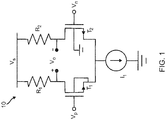
- FIG. 1 illustrates a mismatched differential circuit according to an embodiment of the present invention.
- the mismatched differential circuit 10 of the present embodiment includes a first transistor T 1 and a second transistor T 2 , which have their sources commonly coupled to a current sink I 1 and their drains coupled to a voltage source V s through respective resistors R 1 and R 2 .
- the first and second transistors T 1 and T 2 , the first and second resistors R 1 and R 2 , the voltage source V s , and the current sink I 1 form at least a part of a differential pair amplifier (commonly referred to as a "differential pair"), which has a first amplifying stage and a second amplifying stage that are complementary to each other.
- a differential pair amplifier commonly referred to as a "differential pair”
- the side of the differential pair including the first transistor T 1 corresponds to the first amplifying stage and the side of the differential pair including the second transistor T 2 corresponds to the second amplifying stage.
- the first and second amplifying stages of the differential pair are mismatched. That is, the first amplifying stage has different properties than the second amplifying stage.
- an input offset (or offset voltage) for the differential pair is created, which in turn, may be used to set a threshold level of a comparator.
- the comparator's threshold level may be a function of the particular mismatch in properties of the differential pair at an input stage of a comparator.
- mismatches may arise, for example, from differences is sizing or threshold voltages of the components of the differential pair.
- the mismatches may arise from differences in device sizing or threshold voltages of the first and second transistors T 1 and T 2 .
- V os is the voltage for which the output voltage of the differential pair is zero (i.e., the offset voltage)
- I D is the drain current of the transistors
- g m is the transconductance of the transistors
- W is the width of the transistors
- L is the length of the transistors.
- controlling the input offset via transistor threshold voltage V th is particularly attractive as it directly appears at the input as an offset and may be implemented efficiently with minimal additional circuit complexity.
- controlling the bulk potential of the transistors of the differential pair in a static or dynamic fashion sets (or partially sets) the offset voltage of the differential pair, and thus, extends the achievable range of the threshold level of a comparator.
- the bulk potential of a transistor may be controlled in a static fashion by, for example, hardwiring the bulk of the transistor to a particular node of the transistor (e.g., source), to ground, or to a static voltage source (e.g., a bias voltage).
- a particular node of the transistor e.g., source
- a static voltage source e.g., a bias voltage
- the first and second transistors T 1 and T 2 of the differential circuit 10 of FIG. 1 illustrate example embodiments of static controlled bulk potentials.
- the first transistor T 1 of the present embodiments illustrates a bulk-to-source implementation
- the second transistor T 2 illustrates a bulk-to-ground implementation.
- V th difference in the differential circuit
- this property mismatch sets the offset voltage V os of the differential pair, and thus, controls the threshold level of the comparator.
- the bulk potential may be controlled dynamically by, for example, coupling at least one of the transistor's bulk to an adjustable voltage source.
- an adjustable voltage source By adjusting a transistor's bulk potential with an adjustable voltage source, the difference between the threshold voltages V th of the transistors may be controlled; thus, the offset voltage V os of the differential pair may be dynamically adjusted.
- the difference between the threshold voltages V th may be dynamically controlled by adjusting the effective size (e.g., the effective length or width) of a transistor.
- the width or length of a transistor may be dynamically changed by electronically controlling a series of switches that may be variously connected to adjust the effective width or length of the transistor.
- FIG. 2 is a graph illustrating a relationship between a transistor's bulk-to-source voltage versus its threshold voltage according to an embodiment of the present invention.
- the transistor's threshold voltage V th may be set.
- the threshold voltage V th may be about 470mV, or when the bulk-to-source voltage V BS is set to about -500mV, the threshold voltage V th may be about 575mV.
- the differential circuit further includes two input nodes to receive a complementary pair of input signals V p and V n , respectively, and two output nodes to output the complementary pair of output signals V o+ and V o- , respectively.
- the two input nodes are at the gates of the first and second transistors T 1 and T 2
- the output nodes are at the drains of the first and second transistors T 1 and T 2 .
- the complementary pair of input signals V p and V n (together, the differential input signal) are differentially amplified (i.e., subtracted and multiplied) by the differential pair to generate the complementary pair of output signals V o+ and V o- (together, the differential output signal).
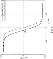
- FIG. 3 is a graph illustrating the I-V characteristics of differential circuits according to embodiments of the present invention.
- FIG. 3 illustrates two example I-V characteristics, one for a balanced differential circuit (indicated by the dashed line) and another for a mismatched differential circuit (indicated by the solid line).
- the x-axis represents a differential input voltage
- the y-axis represents a differential output current for differential circuits.
- a balanced differential circuit e.g., a differential amplifier pair with matching amplifier stages
- the differential output signal is 0V. This is illustrated in FIG. 3 by the zero-crossing of the balanced differential circuit I-V characteristic being at 0V.
- the differential input signal is positive, a negative differential output signal is generated, and when the differential input signal is negative, a positive differential output signal is generated.
- the balanced differential circuit may be used in a comparator circuit having a 0V threshold level. That is, it may be used to detect whether a received differential input signal is less than or greater than 0V.
- a mismatched differential circuit e.g., a differential amplifier with mismatched amplifier stages
- the differential output signal is 0V. This is illustrated in FIG. 3 by the zero-crossing of the mismatched differential circuit I-V characteristic being at the offset voltage V os .
- the differential input signal is greater than the offset voltage V os
- a negative differential output signal is generated
- the differential input signal is less than the offset voltage V os
- a positive differential output signal is generated.
- the mismatched differential circuit may be used in a comparator circuit having a threshold level at (or based on) the offset voltage V os . That is, it may be used to detect whether a received differential input signal is less than or greater than the offset voltage V os .
- the offset voltage V os may be set by adjusting the bulk potential of transistors in the differential circuit.
- embodiments of the present invention are not limited thereto; for example, other methods of adjusting the offset voltage of a differential circuit may be used in conjunction with adjusting the bulk potential.
- the range of achievable comparator threshold levels may be extended by adjusting the size as well as the bulk potential of a device in a differential circuit.
- the device size includes the width and/or length of a channel of a transistor.
- transistors in a differential pair may have mismatched bulk potentials (e.g., one transistor having a bulk-to-source connection and another having a bulk-to-ground connection) and widths (e.g., one transistor having a 15 ⁇ m width and another having a 5 ⁇ m width).
- FIG. 4 is a graph illustrating the I-V characteristics of differential circuits according to other embodiments of the present invention.
- FIG. 4 illustrates four example I-V characteristics, one for a balanced differential circuit (indicated by a line having a dash, two dots, and a dash, repeating, i.e., - ⁇ - ), a second for a bulk mismatched differential circuit (indicated by a line having a dash, one dot, and a dash, repeating, i.e., - ⁇ -), a third for a width mismatched differential circuit (indicated by a dashed line, i.e., - - -), and a fourth for a width and bulk mismatched differential circuit (indicated by a solid line).
- the x-axis represents a differential input voltage
- the y-axis represents a differential output current for differential circuits.
- a balanced differential circuit e.g., a differential amplifier with matching amplifier stages
- the differential output signal is 0V. This is illustrated in FIG. 4 by the zero-crossing of the balanced differential circuit I-V characteristic being at 0V.
- the differential input signal is positive, a negative differential output signal is generated, and when the differential input signal is negative, a positive differential output signal is generated.
- the balanced differential circuit may be used in a comparator circuit having a 0V threshold level. That is, it may be used to detect whether a received differential input signal is less than or greater than 0V.
- a bulk mismatched differential circuit e.g., a differential amplifier with amplifier stages having mismatched bulk potentials
- the differential output signal is 0V. This is illustrated in FIG. 4 by the zero-crossing of the bulk mismatched differential circuit I-V characteristic being at the first offset voltage V os1 .
- the differential input signal is greater than the first offset voltage V os1
- a negative differential output signal is generated
- the differential input signal is less than the first offset voltage V os1
- a positive differential output signal is generated.
- the bulk mismatched differential circuit may be used in a comparator circuit having a threshold level at the first offset voltage V os1 . That is, it may be used to detect whether a received differential input signal is less than or greater than the first offset voltage V os1 .
- a width mismatched differential circuit e.g., a differential amplifier with amplifier stages having mismatched device widths
- the differential output signal is 0V.
- FIG. 4 illustrates in FIG. 4 by the zero-crossing of the width mismatched differential circuit I-V characteristic being at the second offset voltage V os2 .
- the differential input signal is greater than the second offset voltage V os2
- a negative differential output signal is generated
- the differential input signal is less than the second offset voltage V os2
- a positive differential output signal is generated.
- the width mismatched differential circuit may be used in a comparator circuit having a threshold level at the second offset voltage V os2 . That is, it may be used to detect whether a received differential input signal is less than or greater than the second offset voltage V os2 .
- a width and bulk mismatched differential circuit e.g., a differential amplifier with amplifier stages having mismatched device widths and bulk potentials
- the differential output signal is 0V.
- FIG. 4 illustrates in FIG. 4 by the zero-crossing of the width and bulk mismatched differential circuit I-V characteristic being at the third offset voltage V os3 .
- the differential input signal is greater than the third offset voltage V os3
- a negative differential output signal is generated
- the differential input signal is less than the third offset voltage V os3
- a positive differential output signal is generated.
- the bulk and width mismatched differential circuit may be used in a comparator circuit having a threshold level at the third offset voltage V os3 . That is, it may be used to detect whether a received differential input signal is less than or greater than the third offset voltage V os3 .
- offset voltage shifting methods are not limited to adjusting device characteristics.
- offset voltages may be adjusted by controlling current mismatches in a differential circuit.
- FIG. 5 illustrates a mismatched differential circuit for a comparator according to another embodiment of the present invention.
- the mismatched differential circuit 10' of FIG. 5 illustrates an embodiment of the present invention that provides a triple-mismatched differential pair. That is, the mismatched differential circuit 10' illustrates a differential amplifier circuit that may have property mismatches in device bulk potential, device width, and bias current.
- the mismatched differential circuit 10' includes two differential amplifier pairs, each configured substantially similar to the differential amplifier pair described in connection with FIG. 3 .
- the mismatched differential circuit 10' of FIG. 5 includes first through fourth transistors T 1 through T 4 , where each transistor corresponds to one amplifier stage of one of the two amplifier pairs.
- the first transistor T 1 and the second transistor T 2 have their sources commonly coupled to a first current sink I 1 and are coupled to a voltage source V s through respective resistors R 1 and R 2 .
- the first and second transistors T 1 and T 2 correspond to the first differential amplifier pair.
- the third transistor T 3 and the fourth transistor T 4 similarly have their sources commonly coupled to a second current sink I 2 and are coupled to the voltage source V s through respective resistors R 1 and R 2 .
- the third and fourth transistors T 3 and T 4 correspond to the second differential amplifier pair.
- the first and second differential amplifier pairs are coupled together to effectively operate as a single differential amplifier pair. That is, the first and second differential pairs collective receive the same differential input signal and operate together to produce a single differential output signal.
- a feature of using the two coupled differential amplifier pairs is that the different current sinks may be mismatched so as to provide additional offset voltage range.
- the value of the current of the first current sink I 1 may be set to be larger than the value of the current of the second current sink I 2 , which creates an asymmetric amplifying leg resulting in the sought after control of the offset voltage.
- Another feature of using the two coupled differential amplifier pairs is that there are more device parameters available to adjust, which adds further offset voltage flexibility.
- the bulk potentials and/or widths W 1 through W 4 of the transistors may be adjusted so as to enable further flexibility in the available offset voltage.
- the mismatched differential circuits according to embodiments of the present invention may be formed of complementary metal oxide semiconductor (CMOS) devices.
- CMOS complementary metal oxide semiconductor
- the mismatched differential circuits may be formed of N-MOS field effect transistors (FETs).
- FETs field effect transistors
- P-MOS FETs P-MOS field effect transistors
- the bulks of the P-MOS FETs may be coupled to a bias voltage source where, if using N-MOS FETs, the bulks would have been coupled to a ground.
- Multilevel data systems quantize data into more than two levels, thereby using less channel bandwidth than the same capacity binary data system.
- One such multilevel data system is a PAM-4 (pulse amplitude modulation - 4) data system.
- a PAM-4 data system may include a transmitter, a transmission link, and a receiver.
- the PAM-4 transmitter encodes a pair of bits into a four-level signal, for example, V 1 , V 2 , V 3 , and V 4 (e.g., -0.66V, -0.33V, 0.33V, and 0.66V) and sends the encoded multilevel signal over the transmission link to the PAM-4 receiver.
- the PAM-4 receiver reconstructs the transmitted multilevel signal by comparing the received signal to three different threshold voltages, V R1 , V R2 , and V R3 .
- the threshold voltages are determined according to the following logic: V 1 ⁇ V R1 ⁇ V 2 ⁇ V R2 ⁇ V 3 ⁇ V R3 ⁇ V 4 .
- the threshold voltages may be -0.5V, 0V, and 0.5V (e.g., a differential configuration).
- the threshold voltages may be 0.25V, 0.5V, and 0.75V (e.g., a single ended configuration).
- the receiver determines that the multilevel signal is transmitting the logic level associated with V 1 (e.g., 00). If the received multilevel signal is greater than V R1 , but less than V R2 , then the receiver determines that the multilevel signal is transmitting the logic level associated with V 2 (e.g., 01). If the received multilevel signal is greater than V R2 , but less than V R3 , then the receiver determines that the multilevel signal is transmitting the logic level associated with V 3 (e.g., 10). And, if the received multilevel signal is greater than V R2 , then the receiver determines that the multilevel signal is transmitting the logic level associated with V 4 (e.g., 11).
- the multilevel signal is reconstructed by using three comparators, each having a different threshold level, and a decoder.
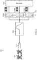
- FIG. 6 illustrates a PAM-4 receiver according to an embodiment of the present invention.
- a pulse amplitude modulation (PAM) receiver 100 includes a transmission link 110 for receiving the multilevel data signal S m (which encodes more than one bit of data), a data slicer 120 that includes a plurality of comparators 130, and a decoder 140.
- the PAM receiver may also include a pre-amplifier 150 to provide gain and equalization to the multilevel data signal S m before it reaches the data slicer 120.
- the multilevel data signal S m is a differential signal.
- a data slicer 120 includes a first comparator 130A that establishes a first threshold voltage V R1 , a second comparator 130B that establishes a second threshold voltage V R2 , and a third comparator 130C that establishes a third threshold voltage V R3 .
- the second threshold voltage V R2 may be greater than the first threshold voltage V R1 and less than the third threshold voltage V R3 .
- the comparators 130A, 130B, and 130C establish these three threshold levels to provide four distinct outputs depending on the relationship of the multilevel data signal S m to the three thresholds. Accordingly, the inputs of the comparators 130A, 130B, and 130C are coupled together to form a common differential input terminal to receive the multilevel data signal S m .
- each of the comparators 130A, 130B, and 130C has a differential output terminal coupled to the decoder 140.
- the decoder 140 receives each of the comparators' 130A, 130B, and 130C differential output signal (e.g., a threshold determination signal) from their respective differential output terminal, and decodes the data transmitted via the multilevel data signal S m based on the received differential output signals.
- a threshold determination signal e.g., a threshold determination signal
- the comparators 130A, 130B, and 130C collectively provide four distinct outputs to the decoder. Each of these outputs corresponds to a particular one of the four signal levels of generated by a PAM-4 transmitter, which encodes two bits of data. Accordingly, the decoder can decode the two bits of data transmitted by the PAM-4 multilevel data signal S m .
- the threshold levels of the comparators 130A, 130B, and 130C are controlled using mismatched differential circuits.
- the first comparator 130A may include a first mismatched differential circuit that has a first offset voltage V os1 to enable the first threshold level voltage V R1
- the second comparator 130B may include a second mismatched differential circuit that has a second offset voltage V os2 to enable the second threshold level voltage V R2
- the third comparator 130C may include a third mismatched differential circuit that has a third offset voltage V os3 to enable the third threshold level voltage V R3 .
- each of the comparators 130A, 130B, and 130C includes a circuit corresponding to the mismatched differential circuit 10 described above in connection with FIGS. 1 through 4 .
- each of the mismatched differential circuits 10 included with the respective comparator 130A, 130B, or 130C has a different offset voltage V os from the other ones in order to provide the three different threshold levels.
- the first comparator 130A may include a width mismatched differential circuit to provide the first threshold level voltage V R1
- the second comparator 130B may include a bulk mismatched differential circuit to provide the second threshold level voltage V R2
- the third comparator may include a width and bulk mismatched differential circuit to provide the third threshold level voltage V R3 .
- each of the mismatched differential circuits is implemented with a circuit corresponding to the mismatched differential circuit 10' described above in connection with FIG. 5 .
- each of the mismatched differential circuits 10' included with the respective comparator 130A, 130B, or 130C has a different offset voltage V os from the other ones in order to provide the three different threshold levels.
- At least one of the mismatched differential circuits 10' may be configured as a triple-mismatched differential pair. That is, at least one of the mismatched differential circuits may have three different mismatched parameters; for example, bulk-potential, device width, and bias current. This enables a wide range of offset voltages V os , and thus, enables a wide range of threshold levels for the comparators.
- FIG. 7 shows graphs illustrating the I-V characteristics of differential circuits according to embodiments of the present invention.
- FIG. 7 illustrates I-V characteristic ranges for three differential circuits. These three I-V characteristic graphs may correspond to the three differential circuits for comparators 130A, 130B, and 130C described above in connection with FIG. 6 . As illustrated in these graphs, the three mismatched differential circuits are configurable to provide a lower, middle, and upper set of offset voltage ranges to correspond to the lower, middle, and upper threshold levels of comparators used in a multilevel receiver.
- the lower and upper mismatched differential circuits are triple-mismatched differential circuits, which are configurable to have bulk potential, device width, and bias current mismatches.
- the lower and upper mismatched differential circuits may be mirrors of each other. That is, amplifier legs in the lower mismatched differential circuit may have a particular mismatch of circuit properties and the amplifier legs in the upper mismatched differential circuit may have a corresponding, but reversed, mismatch of circuit properties (e.g., reversed as to which leg has which circuit properties).
- the lower mismatched differential circuit may be configured such that the first and fourth transistors T 1 and T 4 have a bulk-to-source connection, the second and third T 2 and T 3 transistors have a bulk-to-ground connection, and the first and third transistors' widths W 1 and W 3 are the same size and greater than the second and fourth transistors' widths W 2 and W 4 (which are the same size).
- This configuration results in a first offset voltage V os1 .
- the first offset voltage V os1 may be about -203mV.
- the upper mismatched differential circuit may have a third offset voltage V os3 that is the same magnitude but opposite in polarity as the first offset voltage V os1 .
- the upper mismatched differential circuit may be configured such that the first and fourth transistors T 1 and T 4 have a bulk-to-ground connection, the second and third T 2 and T 3 transistors have a bulk-to-source connection, and the first and third transistors' widths W 1 and W 3 are the same size and less than the second and fourth transistors' widths W 2 and W 4 (which are the same size).
- the third offset voltage V os3 may be about +203mV.
- the lower and upper mismatched differential circuits may have offset voltages of the same magnitude, but with different polarity.
- the middle differential circuit may be configured such that its device properties are matched (i.e., that it is balanced) so that its offset voltage V os2 is at 0V.
- these differential circuits are configurable to have a triple-mismatch by adjusting a bias current.
- the current sinks I 1 and I 2 may be mismatched to further extend the offset voltage range. This may be implemented dynamically or statically.
- the I-V graphs of FIG. 7 illustrate an embodiment of this scenario.
- the x-axis represents a differential input voltage and the y-axis represents a differential output current for the differential circuits.
- the solid line represents a configuration where the bias current is wholly supplied by the first current sink I 1 and the dashed line represents a configuration where the bias current is wholly supplied by the second current sink I 2 .
- the area between these two lines are within the operable range of the mismatched differential circuits, and are achieved by adjusting the mismatch of the first and second current sinks I 1 and I 2 .
- the offset voltage ranges are centered on the offset voltage for the configuration where the bias current is balanced between the first and second current sinks I 1 and I 2 .
- the center of the offset voltage ranges correspond the above-description of the first and third offset voltages V os1 and V os3 respectively corresponding to the mirrored lower and upper mismatched differential circuits and the second offset voltage V os2 corresponding to the balanced middle differential circuit.
- the bias current is about 400 ⁇ A. Therefore, the value of the currents of the first and second current sinks I 1 and I 2 add up to 400 ⁇ A.
- the magnitude of the offset voltage range may be about 600mV.
- an embodiment of the lower mismatched differential circuit may have an offset voltage centered at about -203mV and a range of about -409mV to about 206mV
- an embodiment of the middle mismatched differential circuit may have an offset voltage centered at about 0V and a range of about -306mV to about 306mV
- an embodiment of the upper mismatched differential circuit may have an offset voltage centered at about 203mV and a range of about -206mV to about 409mV.
- comparators having mismatched differential circuits according to embodiments of the present invention when configuring comparators having mismatched differential circuits according to embodiments of the present invention for use in a multilevel signal receiver, a wide range of threshold levels are available.
- FIG. 8 illustrates an exemplary application of a receiver in a digital communication link for a display according to an embodiment of the present invention.
- a display data source 1010 transmits a display data signal over a transmission link 1110 to a display 1020.
- the display data signal may include information for displaying an image on the display.
- the display may be, for example, an organic light emitting diode display, a liquid crystal display, or a plasma display.
- the display 1020 includes a receiver 1100.
- the receiver 1100 may be implemented with the receiver circuit 100 described above in connection with FIGS. 6 and 7 . That is, the receiver 1100 may be implemented using comparators having mismatched differential circuits according to embodiments of the present invention to receive the display data signal transmitted as a multilevel signal.
- embodiments of the present invention were described in connection with a PAM-4 multilevel data system, embodiments of the present invention are not limited thereto. That is, the aspects and features of the present invention may be variously applied, such as in other pulse amplitude modulation systems (e.g., PAM-5, -6, -7, etc.), in digital-to-analog converters, peak-detectors, or any other application that mismatched differential circuits may be used.
Landscapes
- Engineering & Computer Science (AREA)
- Power Engineering (AREA)
- Physics & Mathematics (AREA)
- Nonlinear Science (AREA)
- Spectroscopy & Molecular Physics (AREA)
- Computer Networks & Wireless Communication (AREA)
- Signal Processing (AREA)
- Amplifiers (AREA)
- Manipulation Of Pulses (AREA)
Claims (11)
- Differenzverstärker, umfassend:einen ersten Verstärkerzweig, der einen ersten Transistor (T1) umfasst; undeinen zweiten Verstärkerzweig, der einen zweiten Transistor (T2) umfasst;wobei der erste Transistor (T1) dazu konfiguriert ist, ein Bulkpotenzial aufzuweisen, das sich von einem Bulkpotenzial des zweiten Transistors (T2) unterscheidet;dadurch gekennzeichnet, dass der Differenzverstärker dazu konfiguriert ist, eine Komparatoreingangsstufe zu sein;wobei der erste Verstärkerzweig und der zweite Verstärkerzweig zusammen dazu konfiguriert sind, ein empfangenes Differenzeingangssignal differentiell zu verstärken;wobei der Differenzverstärker dazu konfiguriert ist, eine Eingangsoffsetspannung aufzuweisen;wobei die Eingangsoffsetspannung der Differenz zwischen dem Bulkpotenzial des ersten Transistors und dem Bulkpotenzial des zweiten Transistors entspricht;wobei das Bulkpotenzial zumindest des ersten und/oder des zweiten Transistors so gesteuert wird, dass ein Bereich von Schwellenwertpegeln des Komparators erweiterbar ist;wobei der erste Transistor (T1) eine erste Vorrichtungsgröße aufweist und der zweite Transistor (T2) eine zweite Vorrichtungsgröße, die sich von der ersten Vorrichtungsgröße unterscheidet, aufweist undwobei die Eingangsoffsetspannung ferner der Differenz zwischen der ersten Vorrichtungsgröße und der zweiten Vorrichtungsgröße entspricht.
- Differenzverstärker nach Anspruch 1, wobei die erste Vorrichtungsgröße einer Kanalbreite oder -länge des ersten Transistors (T1) entspricht und die zweite Vorrichtungsgröße einer Kanalbreite oder -länge des zweiten Transistors (T2) entspricht.
- Differenzverstärker nach jeglichem vorangehenden Anspruch, ferner umfassend:eine erste Stromsenke (I1), die dazu konfiguriert ist, einen ersten Strom aufzunehmen;eine zweite Stromsenke (I2), die dazu konfiguriert ist, einen zweiten Strom aufzunehmen;einen dritten Transistor; (T3) undeinen vierten Transistor (T4),wobei sowohl der erste Transistor (T1) als auch der zweite Transistor (T2), der dritte Transistor (T3) und der vierte Transistor (T4) einen ersten Anschluss, einen zweiten Anschluss und ein Gate umfassen,wobei der erste Anschluss des ersten Transistors (T1) mit dem ersten Anschluss des vierten Transistors (T4) gekoppelt ist,wobei der erste Anschluss des zweiten Transistors (T2) mit dem ersten Anschluss des dritten Transistors (T3) gekoppelt ist,wobei das Gate des ersten Transistors (T1) mit dem Gate des vierten Transistors (T4) gekoppelt ist,wobei das Gate des zweiten Transistors (T2) mit dem Gate des dritten Transistors (T3) gekoppelt ist,wobei der zweite Anschluss des ersten Transistors (T1) und der zweite Anschluss des zweiten Transistors (T2) miteinander gekoppelt sind und mit der ersten Stromsenke (I1) gekoppelt sind,wobei der zweite Anschluss des dritten Transistors (T3) und der zweite Anschluss des vierten Transistors (T4) miteinander gekoppelt sind und mit der zweiten Stromsenke (I2) gekoppelt sind undwobei die Eingangsoffsetspannung ferner der Differenz zwischen dem ersten Strom und dem zweiten Strom entspricht.
- Differenzverstärker nach Anspruch 3, wobei die Offsetspannung durch Anpassen zumindest des ersten Stroms, des zweiten Stroms, des Bulkpotenzials des ersten Transistors (T1), des Bulkpotenzials des zweiten Transistors (T2), einer effektiven Breite oder Länge des ersten Transistors (T1) und/oder einer effektiven Breite oder Länge des zweiten Transistors (T2) dynamisch konfigurierbar ist.
- Differenzverstärker nach Anspruch 3 oder 4,
wobei der erste Transistor (T1) und der dritte Transistor (T3) eine erste Vorrichtungsgröße aufweisen,
wobei sowohl der zweite Transistor (T2) als auch der vierte Transistor (T4) eine zweite Vorrichtungsgröße, die sich von der ersten Vorrichtungsgröße unterscheidet, aufweisen und
wobei die Eingangsoffsetspannung ferner der Differenz zwischen der ersten Vorrichtungsgröße und der zweiten Vorrichtungsgröße entspricht. - Differenzverstärker nach Anspruch 1,
wobei sowohl der erste Transistor (T1) als auch der zweite Transistor (T2) ein Feldeffekttransistor sind und ein Bulk, ein Gate, eine Drain und eine Source umfassen,
wobei das Bulk des ersten Transistors (T1) mit der Source des ersten Transistors (T1), einer Masse oder einer Vorspannungsquelle gekoppelt ist,
wobei das Bulk des zweiten Transistors (T2) mit der Source des zweiten Transistors (T2), der Masse oder der Vorspannungsquelle gekoppelt ist und
wobei das Bulk des ersten Transistors (T1) anders als das Bulk des zweiten Transistors (T2) gekoppelt ist, um zu bewirken, dass sich das Bulkpotenzial des ersten Transistors (T1) vom Bulkpotenzial des zweiten Transistors (T2) unterscheidet. - Differenzverstärker nach Anspruch 6,
wobei sowohl der erste Transistor (T1) als auch der zweite Transistor (T2) ein P-MOS-Feldeffekttransistor sind,
wobei das Bulk des ersten Transistors (T1) mit der Source des ersten Transistors (T1) gekoppelt ist und
wobei das Bulk des zweiten Transistors (T2) mit der Vorspannungsquelle gekoppelt ist. - Differenzverstärker nach Anspruch 6,
wobei sowohl der erste Transistor (T1) als auch der zweite Transistor (T2) ein N-MOS-Feldeffekttransistor sind,
wobei das Bulk des ersten Transistors (T1) mit der Source des ersten Transistors (T1) gekoppelt ist und
wobei das Bulk des zweiten Transistors (T2) mit der Masse gekoppelt ist. - Differenzverstärker nach Anspruch 6,
wobei das Bulk des ersten Transistors (T1) mit der Vorspannungsquelle gekoppelt ist,
wobei das Bulk des zweiten Transistors (T2) mit der Masse gekoppelt ist und
wobei die Vorspannungsquelle steuerbar ist, um die Differenz zwischen dem Bulkpotenzial des ersten Transistors (T1) und dem Bulkpotenzial des zweiten Transistors dynamisch zu ändern. - Mehrstufensignalempfänger, umfassend:einen Eingangsanschluss zum Empfangen eines Mehrstufendifferenzsignals;einen Datenschneider, der mit dem Eingangsanschluss gekoppelt und dazu konfiguriert ist, Spannungspegel des Mehrstufendifferenzsignals zu bestimmen, wobei der Datenschneider eine Mehrzahl von Komparatoren umfasst; undeinen Decodierer, der mit einem Ausgang des Datenschneiders gekoppelt und dazu konfiguriert ist, Bits des Mehrstufendifferenzsignals zu decodieren,wobei jeder der Komparatoren einen Differenzverstärker umfasst, wobei zumindest einer der Differenzverstärker einer gemäß einem der vorangehenden Ansprüche ist;wobei jeder der Komparatoren dazu konfiguriert ist, einen Schwellenwertpegel aufzuweisen, der sich vom Schwellenwertpegel anderer der Komparatoren unterscheidet,wobei jeder der Komparatoren dazu konfiguriert ist, sein Schwellenwertbestimmungssignal an den Decodierer auszugeben, um anzuzeigen, ob das Mehrstufensignal größer als sein Schwellenwertpegel ist oder nicht, undwobei beim jedem der Komparatoren der Schwellenwertpegel der Eingangsoffsetspannung des Differenzverstärkers entspricht.
- Mehrstufensignalempfänger nach Anspruch 10,
wobei die Mehrzahl von Komparatoren einen ersten Komparator, dessen Schwellenwertpegel auf einen ersten Pegel eingestellt ist, einen zweiten Komparator, dessen Schwellenwertpegel auf einen zweiten Pegel eingestellt ist, und einen dritten Komparator, dessen Schwellenwertpegel auf einen dritten Pegel eingestellt ist, umfasst,
wobei das Mehrstufensignal dazu konfiguriert ist, zwei Bits unter Verwendung von vier Signalpegeln zu codieren und wobei der erste Pegel, der zweite Pegel und der dritte Pegel jeweils zum Erfassen der vier Signalpegel eingestellt sind.
Applications Claiming Priority (2)
| Application Number | Priority Date | Filing Date | Title |
|---|---|---|---|
| US201361814756P | 2013-04-22 | 2013-04-22 | |
| US14/061,637 US9680430B2 (en) | 2013-04-22 | 2013-10-23 | Mismatched differential circuit |
Publications (2)
| Publication Number | Publication Date |
|---|---|
| EP2797231A1 EP2797231A1 (de) | 2014-10-29 |
| EP2797231B1 true EP2797231B1 (de) | 2018-10-10 |
Family
ID=50543471
Family Applications (1)
| Application Number | Title | Priority Date | Filing Date |
|---|---|---|---|
| EP14165501.9A Active EP2797231B1 (de) | 2013-04-22 | 2014-04-22 | Unterschiedliche Differenzschaltung |
Country Status (7)
| Country | Link |
|---|---|
| US (1) | US9680430B2 (de) |
| EP (1) | EP2797231B1 (de) |
| JP (1) | JP6498386B2 (de) |
| KR (1) | KR102240295B1 (de) |
| CN (1) | CN104113310B (de) |
| AU (1) | AU2014202097B2 (de) |
| TW (1) | TWI634739B (de) |
Families Citing this family (6)
| Publication number | Priority date | Publication date | Assignee | Title |
|---|---|---|---|---|
| CN104734677B (zh) * | 2015-04-14 | 2017-05-24 | 无锡中感微电子股份有限公司 | 单级比较器 |
| CN110637415B (zh) * | 2017-05-31 | 2024-10-01 | 株式会社半导体能源研究所 | 比较电路、半导体装置、电子构件以及电子设备 |
| KR102409877B1 (ko) * | 2017-12-21 | 2022-06-20 | 에스케이하이닉스 주식회사 | 수신 회로 및 이를 이용하는 집적 회로 시스템 |
| CN111969963B (zh) * | 2020-09-10 | 2021-04-09 | 苏州纳芯微电子股份有限公司 | 前置放大器 |
| CN116846371B (zh) | 2022-03-23 | 2025-05-30 | 长鑫存储技术有限公司 | 比较器电路、失配校正方法和存储器 |
| CN116938159A (zh) * | 2023-09-19 | 2023-10-24 | 微龛(广州)半导体有限公司 | 差分输入的电路、差分对失配噪声补偿电路及方法 |
Family Cites Families (27)
| Publication number | Priority date | Publication date | Assignee | Title |
|---|---|---|---|---|
| JPH02234504A (ja) * | 1989-03-07 | 1990-09-17 | Nec Corp | 差動増幅器 |
| US5726597A (en) * | 1996-08-30 | 1998-03-10 | Motorola, Inc. | Method and circuit for reducing offset voltages for a differential input stage |
| AU9014298A (en) | 1997-08-01 | 1999-02-22 | Lsi Logic Corporation | Offset adjustment of cmos matched pairs with body voltage |
| US6262625B1 (en) | 1999-10-29 | 2001-07-17 | Hewlett-Packard Co | Operational amplifier with digital offset calibration |
| WO1999059543A1 (en) | 1998-05-20 | 1999-11-25 | Highchem Company., Ltd. | A pharmaceutical formulation for nasal administration |
| US6222395B1 (en) | 1999-01-04 | 2001-04-24 | International Business Machines Corporation | Single-ended semiconductor receiver with built in threshold voltage difference |
| KR100366616B1 (ko) * | 1999-05-19 | 2003-01-09 | 삼성전자 주식회사 | 저전압 인터페이스용 고속 입력버퍼 회로 |
| US6362687B2 (en) | 1999-05-24 | 2002-03-26 | Science & Technology Corporation | Apparatus for and method of controlling amplifier output offset using body biasing in MOS transistors |
| JP2003273711A (ja) * | 2002-03-12 | 2003-09-26 | Seiko Instruments Inc | 電圧比較器 |
| JP2003318670A (ja) * | 2002-04-26 | 2003-11-07 | Sony Corp | 比較回路および光通信受信装置 |
| KR100496315B1 (ko) * | 2003-03-26 | 2005-06-17 | (주)엠씨에스로직 | 고슬루율 에러 증폭회로 |
| US7283596B2 (en) | 2003-07-08 | 2007-10-16 | Avago Technologies General Ip (Singapore) Pte Ltd | PAM-4 data slicer having symmetrical offset |
| US7091783B2 (en) | 2004-01-14 | 2006-08-15 | Agere Systems Inc. | Rejection circuitry for variable-gain amplifiers and continuous-time filters |
| US7193467B2 (en) * | 2004-03-30 | 2007-03-20 | Rambus Inc. | Differential amplifiers and methods of using same |
| US6927714B1 (en) | 2004-03-31 | 2005-08-09 | Maxim Integrated Products, Inc. | Current steering digital-to-analog (DAC) converter with improved dynamic performance |
| KR100674912B1 (ko) * | 2004-09-24 | 2007-01-26 | 삼성전자주식회사 | 슬루 레이트(slew rate)를 개선시킨 차동 증폭회로 |
| JP4920219B2 (ja) | 2005-08-30 | 2012-04-18 | 株式会社東芝 | 演算増幅器 |
| KR100804650B1 (ko) * | 2006-01-20 | 2008-02-20 | 삼성전자주식회사 | 래치를 가지는 차동-단일 컨버터 및 이를 구비한 위상동기루프 회로 |
| US7629848B2 (en) | 2006-07-07 | 2009-12-08 | Broadcom Corporation | Operational amplifier with extended common-mode input range |
| US7792185B2 (en) | 2007-02-07 | 2010-09-07 | International Business Machines Corporation | Methods and apparatus for calibrating output voltage levels associated with current-integrating summing amplifier |
| KR101330751B1 (ko) * | 2007-02-08 | 2013-11-18 | 삼성전자주식회사 | 클래스 ab 출력 스테이지를 갖는 투-스테이지 연산증폭기 |
| US7843264B2 (en) * | 2008-01-29 | 2010-11-30 | Qualcomm, Incorporated | Differential amplifier with accurate input offset voltage |
| US7920027B2 (en) | 2008-04-07 | 2011-04-05 | Qualcomm Incorporated | Amplifier design with biasing and power control aspects |
| JP4936198B2 (ja) * | 2008-12-12 | 2012-05-23 | ソーバス株式会社 | ラッチ型コンパレータ及びこれを用いた多値論理復調回路 |
| US8222954B1 (en) | 2009-01-29 | 2012-07-17 | Xilinx, Inc. | Method and apparatus for a process, voltage, and temperature variation tolerant semiconductor device |
| US8350622B2 (en) | 2009-11-19 | 2013-01-08 | Stmicroelectronics International N.V. | Output common mode voltage stabilizer over large common mode input range in a high speed differential amplifier |
| TWI479800B (zh) * | 2010-09-27 | 2015-04-01 | Novatek Microelectronics Corp | 差動放大器電路 |
-
2013
- 2013-10-23 US US14/061,637 patent/US9680430B2/en active Active
-
2014
- 2014-04-15 JP JP2014083242A patent/JP6498386B2/ja active Active
- 2014-04-15 AU AU2014202097A patent/AU2014202097B2/en active Active
- 2014-04-22 KR KR1020140048285A patent/KR102240295B1/ko active Active
- 2014-04-22 TW TW103114455A patent/TWI634739B/zh active
- 2014-04-22 EP EP14165501.9A patent/EP2797231B1/de active Active
- 2014-04-22 CN CN201410163658.4A patent/CN104113310B/zh active Active
Non-Patent Citations (1)
| Title |
|---|
| None * |
Also Published As
| Publication number | Publication date |
|---|---|
| TWI634739B (zh) | 2018-09-01 |
| EP2797231A1 (de) | 2014-10-29 |
| CN104113310A (zh) | 2014-10-22 |
| US9680430B2 (en) | 2017-06-13 |
| CN104113310B (zh) | 2018-05-29 |
| AU2014202097B2 (en) | 2017-09-28 |
| KR20140126268A (ko) | 2014-10-30 |
| US20140314171A1 (en) | 2014-10-23 |
| JP2014217056A (ja) | 2014-11-17 |
| AU2014202097A1 (en) | 2014-11-06 |
| KR102240295B1 (ko) | 2021-04-14 |
| TW201501463A (zh) | 2015-01-01 |
| JP6498386B2 (ja) | 2019-04-10 |
Similar Documents
| Publication | Publication Date | Title |
|---|---|---|
| EP2797231B1 (de) | Unterschiedliche Differenzschaltung | |
| US9746864B1 (en) | Fast transient low drop-out voltage regulator for a voltage-mode driver | |
| US9344305B2 (en) | PVT tolerant differential circuit | |
| US10270630B2 (en) | Demodulation of on-off-key modulated signals in signal isolator systems | |
| US10536309B2 (en) | Demodulation of on-off-key modulated signals in signal isolator systems | |
| US9716480B2 (en) | Trans-impedance amplifier with replica gain control | |
| KR20070115759A (ko) | 출력 회로를 구비하는 반도체 집적 회로 | |
| US7339421B2 (en) | Differential circuit and receiver with same | |
| JP2017511061A (ja) | コモンレベルシフティングためのシステム及び方法 | |
| JP2018527787A (ja) | トランスミッタにおいて変調信号を生成するための回路および方法 | |
| US20160241235A1 (en) | Transmission circuit and semiconductor integrated circuit | |
| US8130034B2 (en) | Rail-to-rail amplifier | |
| US9559697B2 (en) | Transmitter circuit and semiconductor integrated circuit | |
| US20180145650A1 (en) | Split cascode circuits and related communication receiver architectures | |
| US20090091357A1 (en) | Low voltage differential signalling driver | |
| CN104283518B (zh) | 工艺、电压和温度耐受差分电路 | |
| KR20010080431A (ko) | 데이터 종속 전압 바이어스 레벨을 위한 회로 | |
| EP2830214B1 (de) | PVT-tolerante Differenzialschaltung | |
| US8008972B2 (en) | Differential signal generator circuit | |
| US9843297B2 (en) | Balanced differential transimpedance amplifier with single ended input and balancing method | |
| US10404228B2 (en) | Transconductance amplifier and phase shifter | |
| TW201810937A (zh) | 適於寬輸入範圍應用的跨導運算放大器 | |
| JP2015216476A (ja) | ドライバ回路 | |
| WO2007020709A1 (ja) | 半導体装置 |
Legal Events
| Date | Code | Title | Description |
|---|---|---|---|
| PUAI | Public reference made under article 153(3) epc to a published international application that has entered the european phase |
Free format text: ORIGINAL CODE: 0009012 |
|
| 17P | Request for examination filed |
Effective date: 20140422 |
|
| AK | Designated contracting states |
Kind code of ref document: A1 Designated state(s): AL AT BE BG CH CY CZ DE DK EE ES FI FR GB GR HR HU IE IS IT LI LT LU LV MC MK MT NL NO PL PT RO RS SE SI SK SM TR |
|
| AX | Request for extension of the european patent |
Extension state: BA ME |
|
| R17P | Request for examination filed (corrected) |
Effective date: 20150428 |
|
| RBV | Designated contracting states (corrected) |
Designated state(s): AL AT BE BG CH CY CZ DE DK EE ES FI FR GB GR HR HU IE IS IT LI LT LU LV MC MK MT NL NO PL PT RO RS SE SI SK SM TR |
|
| RAP1 | Party data changed (applicant data changed or rights of an application transferred) |
Owner name: SAMSUNG DISPLAY CO., LTD. |
|
| 17Q | First examination report despatched |
Effective date: 20160211 |
|
| STAA | Information on the status of an ep patent application or granted ep patent |
Free format text: STATUS: EXAMINATION IS IN PROGRESS |
|
| GRAP | Despatch of communication of intention to grant a patent |
Free format text: ORIGINAL CODE: EPIDOSNIGR1 |
|
| STAA | Information on the status of an ep patent application or granted ep patent |
Free format text: STATUS: GRANT OF PATENT IS INTENDED |
|
| INTG | Intention to grant announced |
Effective date: 20180423 |
|
| GRAS | Grant fee paid |
Free format text: ORIGINAL CODE: EPIDOSNIGR3 |
|
| GRAJ | Information related to disapproval of communication of intention to grant by the applicant or resumption of examination proceedings by the epo deleted |
Free format text: ORIGINAL CODE: EPIDOSDIGR1 |
|
| GRAL | Information related to payment of fee for publishing/printing deleted |
Free format text: ORIGINAL CODE: EPIDOSDIGR3 |
|
| STAA | Information on the status of an ep patent application or granted ep patent |
Free format text: STATUS: EXAMINATION IS IN PROGRESS |
|
| GRAR | Information related to intention to grant a patent recorded |
Free format text: ORIGINAL CODE: EPIDOSNIGR71 |
|
| STAA | Information on the status of an ep patent application or granted ep patent |
Free format text: STATUS: GRANT OF PATENT IS INTENDED |
|
| GRAA | (expected) grant |
Free format text: ORIGINAL CODE: 0009210 |
|
| STAA | Information on the status of an ep patent application or granted ep patent |
Free format text: STATUS: THE PATENT HAS BEEN GRANTED |
|
| INTC | Intention to grant announced (deleted) | ||
| AK | Designated contracting states |
Kind code of ref document: B1 Designated state(s): AL AT BE BG CH CY CZ DE DK EE ES FI FR GB GR HR HU IE IS IT LI LT LU LV MC MK MT NL NO PL PT RO RS SE SI SK SM TR |
|
| INTG | Intention to grant announced |
Effective date: 20180903 |
|
| REG | Reference to a national code |
Ref country code: GB Ref legal event code: FG4D |
|
| REG | Reference to a national code |
Ref country code: CH Ref legal event code: EP Ref country code: AT Ref legal event code: REF Ref document number: 1052429 Country of ref document: AT Kind code of ref document: T Effective date: 20181015 |
|
| REG | Reference to a national code |
Ref country code: IE Ref legal event code: FG4D |
|
| REG | Reference to a national code |
Ref country code: DE Ref legal event code: R096 Ref document number: 602014033655 Country of ref document: DE |
|
| REG | Reference to a national code |
Ref country code: NL Ref legal event code: MP Effective date: 20181010 |
|
| REG | Reference to a national code |
Ref country code: LT Ref legal event code: MG4D |
|
| REG | Reference to a national code |
Ref country code: AT Ref legal event code: MK05 Ref document number: 1052429 Country of ref document: AT Kind code of ref document: T Effective date: 20181010 |
|
| PG25 | Lapsed in a contracting state [announced via postgrant information from national office to epo] |
Ref country code: NL Free format text: LAPSE BECAUSE OF FAILURE TO SUBMIT A TRANSLATION OF THE DESCRIPTION OR TO PAY THE FEE WITHIN THE PRESCRIBED TIME-LIMIT Effective date: 20181010 |
|
| PG25 | Lapsed in a contracting state [announced via postgrant information from national office to epo] |
Ref country code: FI Free format text: LAPSE BECAUSE OF FAILURE TO SUBMIT A TRANSLATION OF THE DESCRIPTION OR TO PAY THE FEE WITHIN THE PRESCRIBED TIME-LIMIT Effective date: 20181010 Ref country code: BG Free format text: LAPSE BECAUSE OF FAILURE TO SUBMIT A TRANSLATION OF THE DESCRIPTION OR TO PAY THE FEE WITHIN THE PRESCRIBED TIME-LIMIT Effective date: 20190110 Ref country code: PL Free format text: LAPSE BECAUSE OF FAILURE TO SUBMIT A TRANSLATION OF THE DESCRIPTION OR TO PAY THE FEE WITHIN THE PRESCRIBED TIME-LIMIT Effective date: 20181010 Ref country code: HR Free format text: LAPSE BECAUSE OF FAILURE TO SUBMIT A TRANSLATION OF THE DESCRIPTION OR TO PAY THE FEE WITHIN THE PRESCRIBED TIME-LIMIT Effective date: 20181010 Ref country code: LV Free format text: LAPSE BECAUSE OF FAILURE TO SUBMIT A TRANSLATION OF THE DESCRIPTION OR TO PAY THE FEE WITHIN THE PRESCRIBED TIME-LIMIT Effective date: 20181010 Ref country code: AT Free format text: LAPSE BECAUSE OF FAILURE TO SUBMIT A TRANSLATION OF THE DESCRIPTION OR TO PAY THE FEE WITHIN THE PRESCRIBED TIME-LIMIT Effective date: 20181010 Ref country code: ES Free format text: LAPSE BECAUSE OF FAILURE TO SUBMIT A TRANSLATION OF THE DESCRIPTION OR TO PAY THE FEE WITHIN THE PRESCRIBED TIME-LIMIT Effective date: 20181010 Ref country code: LT Free format text: LAPSE BECAUSE OF FAILURE TO SUBMIT A TRANSLATION OF THE DESCRIPTION OR TO PAY THE FEE WITHIN THE PRESCRIBED TIME-LIMIT Effective date: 20181010 Ref country code: IS Free format text: LAPSE BECAUSE OF FAILURE TO SUBMIT A TRANSLATION OF THE DESCRIPTION OR TO PAY THE FEE WITHIN THE PRESCRIBED TIME-LIMIT Effective date: 20190210 Ref country code: NO Free format text: LAPSE BECAUSE OF FAILURE TO SUBMIT A TRANSLATION OF THE DESCRIPTION OR TO PAY THE FEE WITHIN THE PRESCRIBED TIME-LIMIT Effective date: 20190110 |
|
| PG25 | Lapsed in a contracting state [announced via postgrant information from national office to epo] |
Ref country code: PT Free format text: LAPSE BECAUSE OF FAILURE TO SUBMIT A TRANSLATION OF THE DESCRIPTION OR TO PAY THE FEE WITHIN THE PRESCRIBED TIME-LIMIT Effective date: 20190210 Ref country code: AL Free format text: LAPSE BECAUSE OF FAILURE TO SUBMIT A TRANSLATION OF THE DESCRIPTION OR TO PAY THE FEE WITHIN THE PRESCRIBED TIME-LIMIT Effective date: 20181010 Ref country code: GR Free format text: LAPSE BECAUSE OF FAILURE TO SUBMIT A TRANSLATION OF THE DESCRIPTION OR TO PAY THE FEE WITHIN THE PRESCRIBED TIME-LIMIT Effective date: 20190111 Ref country code: RS Free format text: LAPSE BECAUSE OF FAILURE TO SUBMIT A TRANSLATION OF THE DESCRIPTION OR TO PAY THE FEE WITHIN THE PRESCRIBED TIME-LIMIT Effective date: 20181010 Ref country code: SE Free format text: LAPSE BECAUSE OF FAILURE TO SUBMIT A TRANSLATION OF THE DESCRIPTION OR TO PAY THE FEE WITHIN THE PRESCRIBED TIME-LIMIT Effective date: 20181010 |
|
| REG | Reference to a national code |
Ref country code: DE Ref legal event code: R097 Ref document number: 602014033655 Country of ref document: DE |
|
| PG25 | Lapsed in a contracting state [announced via postgrant information from national office to epo] |
Ref country code: IT Free format text: LAPSE BECAUSE OF FAILURE TO SUBMIT A TRANSLATION OF THE DESCRIPTION OR TO PAY THE FEE WITHIN THE PRESCRIBED TIME-LIMIT Effective date: 20181010 Ref country code: CZ Free format text: LAPSE BECAUSE OF FAILURE TO SUBMIT A TRANSLATION OF THE DESCRIPTION OR TO PAY THE FEE WITHIN THE PRESCRIBED TIME-LIMIT Effective date: 20181010 Ref country code: DK Free format text: LAPSE BECAUSE OF FAILURE TO SUBMIT A TRANSLATION OF THE DESCRIPTION OR TO PAY THE FEE WITHIN THE PRESCRIBED TIME-LIMIT Effective date: 20181010 |
|
| PLBE | No opposition filed within time limit |
Free format text: ORIGINAL CODE: 0009261 |
|
| STAA | Information on the status of an ep patent application or granted ep patent |
Free format text: STATUS: NO OPPOSITION FILED WITHIN TIME LIMIT |
|
| PG25 | Lapsed in a contracting state [announced via postgrant information from national office to epo] |
Ref country code: EE Free format text: LAPSE BECAUSE OF FAILURE TO SUBMIT A TRANSLATION OF THE DESCRIPTION OR TO PAY THE FEE WITHIN THE PRESCRIBED TIME-LIMIT Effective date: 20181010 Ref country code: SM Free format text: LAPSE BECAUSE OF FAILURE TO SUBMIT A TRANSLATION OF THE DESCRIPTION OR TO PAY THE FEE WITHIN THE PRESCRIBED TIME-LIMIT Effective date: 20181010 Ref country code: SK Free format text: LAPSE BECAUSE OF FAILURE TO SUBMIT A TRANSLATION OF THE DESCRIPTION OR TO PAY THE FEE WITHIN THE PRESCRIBED TIME-LIMIT Effective date: 20181010 Ref country code: RO Free format text: LAPSE BECAUSE OF FAILURE TO SUBMIT A TRANSLATION OF THE DESCRIPTION OR TO PAY THE FEE WITHIN THE PRESCRIBED TIME-LIMIT Effective date: 20181010 |
|
| 26N | No opposition filed |
Effective date: 20190711 |
|
| PG25 | Lapsed in a contracting state [announced via postgrant information from national office to epo] |
Ref country code: SI Free format text: LAPSE BECAUSE OF FAILURE TO SUBMIT A TRANSLATION OF THE DESCRIPTION OR TO PAY THE FEE WITHIN THE PRESCRIBED TIME-LIMIT Effective date: 20181010 |
|
| REG | Reference to a national code |
Ref country code: CH Ref legal event code: PL |
|
| REG | Reference to a national code |
Ref country code: BE Ref legal event code: MM Effective date: 20190430 |
|
| PG25 | Lapsed in a contracting state [announced via postgrant information from national office to epo] |
Ref country code: MC Free format text: LAPSE BECAUSE OF FAILURE TO SUBMIT A TRANSLATION OF THE DESCRIPTION OR TO PAY THE FEE WITHIN THE PRESCRIBED TIME-LIMIT Effective date: 20181010 Ref country code: LU Free format text: LAPSE BECAUSE OF NON-PAYMENT OF DUE FEES Effective date: 20190422 |
|
| PG25 | Lapsed in a contracting state [announced via postgrant information from national office to epo] |
Ref country code: LI Free format text: LAPSE BECAUSE OF NON-PAYMENT OF DUE FEES Effective date: 20190430 Ref country code: CH Free format text: LAPSE BECAUSE OF NON-PAYMENT OF DUE FEES Effective date: 20190430 |
|
| PG25 | Lapsed in a contracting state [announced via postgrant information from national office to epo] |
Ref country code: BE Free format text: LAPSE BECAUSE OF NON-PAYMENT OF DUE FEES Effective date: 20190430 |
|
| PG25 | Lapsed in a contracting state [announced via postgrant information from national office to epo] |
Ref country code: TR Free format text: LAPSE BECAUSE OF FAILURE TO SUBMIT A TRANSLATION OF THE DESCRIPTION OR TO PAY THE FEE WITHIN THE PRESCRIBED TIME-LIMIT Effective date: 20181010 |
|
| PG25 | Lapsed in a contracting state [announced via postgrant information from national office to epo] |
Ref country code: IE Free format text: LAPSE BECAUSE OF NON-PAYMENT OF DUE FEES Effective date: 20190422 |
|
| PG25 | Lapsed in a contracting state [announced via postgrant information from national office to epo] |
Ref country code: CY Free format text: LAPSE BECAUSE OF FAILURE TO SUBMIT A TRANSLATION OF THE DESCRIPTION OR TO PAY THE FEE WITHIN THE PRESCRIBED TIME-LIMIT Effective date: 20181010 |
|
| PG25 | Lapsed in a contracting state [announced via postgrant information from national office to epo] |
Ref country code: HU Free format text: LAPSE BECAUSE OF FAILURE TO SUBMIT A TRANSLATION OF THE DESCRIPTION OR TO PAY THE FEE WITHIN THE PRESCRIBED TIME-LIMIT; INVALID AB INITIO Effective date: 20140422 Ref country code: MT Free format text: LAPSE BECAUSE OF FAILURE TO SUBMIT A TRANSLATION OF THE DESCRIPTION OR TO PAY THE FEE WITHIN THE PRESCRIBED TIME-LIMIT Effective date: 20181010 |
|
| PG25 | Lapsed in a contracting state [announced via postgrant information from national office to epo] |
Ref country code: MK Free format text: LAPSE BECAUSE OF FAILURE TO SUBMIT A TRANSLATION OF THE DESCRIPTION OR TO PAY THE FEE WITHIN THE PRESCRIBED TIME-LIMIT Effective date: 20181010 |
|
| P01 | Opt-out of the competence of the unified patent court (upc) registered |
Effective date: 20230516 |
|
| PGFP | Annual fee paid to national office [announced via postgrant information from national office to epo] |
Ref country code: DE Payment date: 20250320 Year of fee payment: 12 |
|
| PGFP | Annual fee paid to national office [announced via postgrant information from national office to epo] |
Ref country code: GB Payment date: 20260324 Year of fee payment: 13 |
|
| PGFP | Annual fee paid to national office [announced via postgrant information from national office to epo] |
Ref country code: FR Payment date: 20260323 Year of fee payment: 13 |