EP2797124B1 - Verfahren zur Herstellung einer Solarzelle - Google Patents
Verfahren zur Herstellung einer Solarzelle Download PDFInfo
- Publication number
- EP2797124B1 EP2797124B1 EP14001446.5A EP14001446A EP2797124B1 EP 2797124 B1 EP2797124 B1 EP 2797124B1 EP 14001446 A EP14001446 A EP 14001446A EP 2797124 B1 EP2797124 B1 EP 2797124B1
- Authority
- EP
- European Patent Office
- Prior art keywords
- conductive type
- layer
- area
- doping
- forming
- Prior art date
- Legal status (The legal status is an assumption and is not a legal conclusion. Google has not performed a legal analysis and makes no representation as to the accuracy of the status listed.)
- Active
Links
Images


Classifications
-
- H—ELECTRICITY
- H10—SEMICONDUCTOR DEVICES; ELECTRIC SOLID-STATE DEVICES NOT OTHERWISE PROVIDED FOR
- H10F—INORGANIC SEMICONDUCTOR DEVICES SENSITIVE TO INFRARED RADIATION, LIGHT, ELECTROMAGNETIC RADIATION OF SHORTER WAVELENGTH OR CORPUSCULAR RADIATION
- H10F10/00—Individual photovoltaic cells, e.g. solar cells
- H10F10/10—Individual photovoltaic cells, e.g. solar cells having potential barriers
-
- H—ELECTRICITY
- H10—SEMICONDUCTOR DEVICES; ELECTRIC SOLID-STATE DEVICES NOT OTHERWISE PROVIDED FOR
- H10F—INORGANIC SEMICONDUCTOR DEVICES SENSITIVE TO INFRARED RADIATION, LIGHT, ELECTROMAGNETIC RADIATION OF SHORTER WAVELENGTH OR CORPUSCULAR RADIATION
- H10F77/00—Constructional details of devices covered by this subclass
- H10F77/30—Coatings
- H10F77/306—Coatings for devices having potential barriers
- H10F77/311—Coatings for devices having potential barriers for photovoltaic cells
-
- H—ELECTRICITY
- H10—SEMICONDUCTOR DEVICES; ELECTRIC SOLID-STATE DEVICES NOT OTHERWISE PROVIDED FOR
- H10F—INORGANIC SEMICONDUCTOR DEVICES SENSITIVE TO INFRARED RADIATION, LIGHT, ELECTROMAGNETIC RADIATION OF SHORTER WAVELENGTH OR CORPUSCULAR RADIATION
- H10F10/00—Individual photovoltaic cells, e.g. solar cells
- H10F10/10—Individual photovoltaic cells, e.g. solar cells having potential barriers
- H10F10/16—Photovoltaic cells having only PN heterojunction potential barriers
- H10F10/164—Photovoltaic cells having only PN heterojunction potential barriers comprising heterojunctions with Group IV materials, e.g. ITO/Si or GaAs/SiGe photovoltaic cells
- H10F10/165—Photovoltaic cells having only PN heterojunction potential barriers comprising heterojunctions with Group IV materials, e.g. ITO/Si or GaAs/SiGe photovoltaic cells the heterojunctions being Group IV-IV heterojunctions, e.g. Si/Ge, SiGe/Si or Si/SiC photovoltaic cells
- H10F10/166—Photovoltaic cells having only PN heterojunction potential barriers comprising heterojunctions with Group IV materials, e.g. ITO/Si or GaAs/SiGe photovoltaic cells the heterojunctions being Group IV-IV heterojunctions, e.g. Si/Ge, SiGe/Si or Si/SiC photovoltaic cells the Group IV-IV heterojunctions being heterojunctions of crystalline and amorphous materials, e.g. silicon heterojunction [SHJ] photovoltaic cells
-
- H—ELECTRICITY
- H10—SEMICONDUCTOR DEVICES; ELECTRIC SOLID-STATE DEVICES NOT OTHERWISE PROVIDED FOR
- H10F—INORGANIC SEMICONDUCTOR DEVICES SENSITIVE TO INFRARED RADIATION, LIGHT, ELECTROMAGNETIC RADIATION OF SHORTER WAVELENGTH OR CORPUSCULAR RADIATION
- H10F19/00—Integrated devices, or assemblies of multiple devices, comprising at least one photovoltaic cell covered by group H10F10/00, e.g. photovoltaic modules
-
- H—ELECTRICITY
- H10—SEMICONDUCTOR DEVICES; ELECTRIC SOLID-STATE DEVICES NOT OTHERWISE PROVIDED FOR
- H10F—INORGANIC SEMICONDUCTOR DEVICES SENSITIVE TO INFRARED RADIATION, LIGHT, ELECTROMAGNETIC RADIATION OF SHORTER WAVELENGTH OR CORPUSCULAR RADIATION
- H10F71/00—Manufacture or treatment of devices covered by this subclass
- H10F71/121—The active layers comprising only Group IV materials
-
- H—ELECTRICITY
- H10—SEMICONDUCTOR DEVICES; ELECTRIC SOLID-STATE DEVICES NOT OTHERWISE PROVIDED FOR
- H10F—INORGANIC SEMICONDUCTOR DEVICES SENSITIVE TO INFRARED RADIATION, LIGHT, ELECTROMAGNETIC RADIATION OF SHORTER WAVELENGTH OR CORPUSCULAR RADIATION
- H10F77/00—Constructional details of devices covered by this subclass
- H10F77/20—Electrodes
- H10F77/206—Electrodes for devices having potential barriers
- H10F77/211—Electrodes for devices having potential barriers for photovoltaic cells
- H10F77/219—Arrangements for electrodes of back-contact photovoltaic cells
-
- Y—GENERAL TAGGING OF NEW TECHNOLOGICAL DEVELOPMENTS; GENERAL TAGGING OF CROSS-SECTIONAL TECHNOLOGIES SPANNING OVER SEVERAL SECTIONS OF THE IPC; TECHNICAL SUBJECTS COVERED BY FORMER USPC CROSS-REFERENCE ART COLLECTIONS [XRACs] AND DIGESTS
- Y02—TECHNOLOGIES OR APPLICATIONS FOR MITIGATION OR ADAPTATION AGAINST CLIMATE CHANGE
- Y02E—REDUCTION OF GREENHOUSE GAS [GHG] EMISSIONS, RELATED TO ENERGY GENERATION, TRANSMISSION OR DISTRIBUTION
- Y02E10/00—Energy generation through renewable energy sources
- Y02E10/50—Photovoltaic [PV] energy
- Y02E10/547—Monocrystalline silicon PV cells
-
- Y—GENERAL TAGGING OF NEW TECHNOLOGICAL DEVELOPMENTS; GENERAL TAGGING OF CROSS-SECTIONAL TECHNOLOGIES SPANNING OVER SEVERAL SECTIONS OF THE IPC; TECHNICAL SUBJECTS COVERED BY FORMER USPC CROSS-REFERENCE ART COLLECTIONS [XRACs] AND DIGESTS
- Y02—TECHNOLOGIES OR APPLICATIONS FOR MITIGATION OR ADAPTATION AGAINST CLIMATE CHANGE
- Y02P—CLIMATE CHANGE MITIGATION TECHNOLOGIES IN THE PRODUCTION OR PROCESSING OF GOODS
- Y02P70/00—Climate change mitigation technologies in the production process for final industrial or consumer products
- Y02P70/50—Manufacturing or production processes characterised by the final manufactured product
Definitions
- the present disclosure relates to a method for manufacturing a solar cell and, more particularly, to a method for manufacturing a solar cell having an improved structure.
- Such a solar cell may be manufactured by forming various layers and electrodes according to design. Solar cell efficiency may be determined according to design of various layers and electrodes. Low efficiency should be overcome in order to commercialize solar cells. Various layers and electrodes should be designed so that efficiency of solar cells can be maximized.
- US 2012/0138135 A1 discloses a solar cell comprising a semiconductor substrate, a tunneling layer, a first conductive area on the tunneling layer, a second conductive type area on the tunneling layer, a trench between the first and second conductive type areas and a dielectric layer filling the trench.
- US 2012/0322199 A1 discloses a method wherein a barrier area between first and second conductive type implanted regions is obtained thanks to two masks that are designed to be non-overlapping and to guarantee a gap between said implanted regions.
- a mask and an etch step are used to form a trench between a first conductive type area and a second conductive type area.
- An insulating region is thereafter deposited in the trench.
- a trench and a dielectric layer filling the trench are also provided between the first and second conductive type areas.
- WO 2012/163517 A2 discloses a rear contacted heterojunction intrinsic thin layer solar cell comprising a silicon substrate, a passivating layer, a thin intrinsic amorphous silicon layer, an emitter layer, a base layer and a separation layer, wherein the adjacent regions of the emitter layer and the separating layer and adjacent regions of the baser layer and the separating layer are partially laterally overlapping in such a way that, in an overlapping area, at least a portion of the separating layer is located closer to the substrate than an overlapping portion of the respective one of the emitter layer and the base layer.
- US 2012/0199183 A1 discloses a back contact type solar cell where an insulation pattern for insulating conductive regions of opposite conductive types from each other is formed before forming the conductive regions by using an inkjet printing method.
- a method for manufacturing a solar cell according to the present invention is defined in the claims.
- One object is to provide a method for manufacturing a solar cell which is capable of improving reliability and maximizing efficiency.
- the method for manufacturing a solar cell includes forming a tunneling layer on one surface of a semiconductor substrate, forming a semiconductor layer on the tunneling layer, and doping the semiconductor layer with a first conductive type dopant and a second conductive type dopant to form a first conductive type area and a second conductive type area separated from each other via a barrier area.
- the solar cell obtained according to the method of the present invention includes the barrier area interposed between the first conductive type area and the second conductive type area disposed on one surface (for example, back surface) of the semiconductor substrate.
- the barrier area prevents connection between the first and second conductive type areas to undesired impurity layers, when alignment of the first and second electrodes connected to the first and second conductive type areas, respectively, is not reasonable.
- opening voltage and fill factor of the solar cell are improved and efficiency and power of the solar cell can be thus increased.
- the method for manufacturing a solar cell according to the present embodiment enables formation of the solar cell having a structure in a simple method.
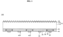
- FIG. 1 is a sectional view of a solar cell according to an example useful for understanding the present invention.
- the solar cell 100 according to the example includes a semiconductor substrate 10, a tunneling layer 20 formed on one surface (for example, back surface) of the semiconductor substrate 10, and a first conductive type area 32, a second conductive type area 34 and a barrier area 36 formed on the tunneling layer 20.
- the first conductive type area 32 and the second conductive type area 34 are spaced from each other via the barrier area 36.
- the solar cell 100 further includes first and second electrodes 42 and 44 which are connected to first and second conductive type areas 32 and 34, respectively, and collect carriers.
- an anti-reflective film 50 may be further formed on another surface of the semiconductor substrate 10. This configuration will be described in detail.
- the semiconductor substrate 10 may include a base area 110 containing a low doping concentration of first conductive type dopant.
- the semiconductor substrate 10 may, for example, include a crystalline semiconductor (for example, crystalline silicon) containing a first conductive-type dopant.
- the crystalline semiconductor may be monocrystalline silicon, and the first conductive-type dopant may be, for example, an n-type or p-type dopant. That is, the first conductive-type dopant may be an n-type impurity such as a Group V element including phosphorous (P), arsenic (As), bismuth (Bi), antimony (Sb) or the like. Alternatively, the first conductive-type dopant may be a p-type impurity such as a Group III element including boron (B), aluminum (Al), gallium (Ga), indium (In) or the like.
- the base area 110 may have an n-type impurity as the first conductive-type dopant.
- the second conductive type area 34 forming a tunnel junction through the tunneling layer 20 with the base area 110 may be a p-type.
- the first conductive type area 32 serving as an emitter causing photoelectric transformation through junction with the base area 110 may be widely formed and, as a result, holes having movement speed lower than electrons can be efficiently collected. Electrons created by photoelectric effect are collected by a first electrode 42 when light is emitted to the tunnel junction, and holes are moved toward the front surface of the semiconductor substrate 10 and are then collected by a second electrode 44. As a result, electric energy is generated, but the present invention is not limited thereto, and the base area 110 and the first conductive type area 32 may be a p-type while the second conductive type area 34 may be an n-type.
- the front surface of the semiconductor substrate 10 is textured to have irregularities having a shape such as a pyramidal shape.
- surface roughness is increased due to irregularities formed on the front surface of the semiconductor substrate 10 through such texturing, reflection of light incident through the front surface of the semiconductor substrate 10 can be reduced. Accordingly, an amount of light which reaches the tunnel junction formed by the semiconductor substrate 10 and the second conductive type area 34 is increased and light loss can thus be minimized.
- the back surface of the semiconductor substrate 10 may be a smooth and even surface having a surface roughness lower than the front surface, obtained through mirror polishing or the like.
- the back surface of the semiconductor substrate 10 may be a smooth and even surface having a surface roughness lower than the front surface, obtained through mirror polishing or the like.
- the front surface field layer 120 is an area where the first conductive-type dopant is doped at a concentration higher than the semiconductor substrate 10 and performs similar functions to a back surface field (BSF) layer. That is, the front surface field layer 120 prevents electrons and holes 'separated by incident light from being recombined and then decay on the front surface of the semiconductor substrate 10.
- the front surface field layer 120 may be omitted. This example will be described in more detail with reference to FIG. 5 .
- an anti-reflective film 50 may be formed on the front surface field layer 120.
- the anti-reflective film 50 may be entirely formed over the front surface of the semiconductor substrate 10.
- the anti-reflective film 50 decreases reflectivity of light incident upon the front surface of the semiconductor substrate 10 and passivates defects present on the surface or in the bulk of the front surface field layer 120.
- the decrease in reflectivity of light incident upon the front surface of the semiconductor substrate 10 causes an increase in amount of light reaching the tunnel junction. Accordingly, short current (Isc) of the solar cell 100 can be increased.
- the anti-reflective film 50 passivates defects, removes recombination sites of minority carriers and thus increases open-circuit voltage (Voc) of the solar cell 100. As such, the anti-reflective film 50 increases open-circuit voltage and short current of the solar cell 100, thus improving conversion efficiency of the solar cell 100.
- the anti-reflective film 50 may be formed of a variety of materials.
- the anti-reflective film 50 may be a single film selected from the group consisting of a silicon nitride film, a silicon nitride film containing hydrogen, a silicon oxide film, a silicon oxide nitride film, MgF 2 , ZnS, TiO 2 and CeO 2 , or a multilayer film including a combination of two or more thereof, but the present disclosure is not limited thereto and the anti-reflective film 50 may include a variety of materials.
- a tunneling layer 20 is formed on the back surface of the semiconductor substrate 10.
- the tunneling layer 20 improves interface properties of the back surface of the semiconductor substrate 10 and enables produced carriers to be efficiently transferred through tunneling effect.
- the tunneling layer 20 may include a variety of materials enabling tunneling of carriers and examples of the materials include oxides, nitrides and conductive polymers.
- the tunneling layer 20 may be entirely formed on the back surface of the semiconductor substrate 10. Accordingly, the tunneling layer 20 entirely passivates the back surface of the semiconductor substrate 10 and can be easily formed without additional patterning.
- a thickness of the tunneling layer 20 may be 5.0 nm or less so that the tunneling layer 20 sufficiently exhibits a tunneling effect, or may be 0.5 nm to 5 nm (for example, 1.0 nm to 4 nm). When the thickness of the tunneling layer 20 exceeds 5 nm, tunneling is not efficiently performed and the solar cell 100 may not operate, and when the thickness of the tunneling layer 20 is less than 0.5 nm, there may be difficulty in formation of the tunneling layer 20 with desired qualities. In order to further improve the tunneling effect, the thickness of the tunneling layer 20 may be 1.0 nm to 4.0 nm, but the present invention is not limited thereto and the thickness of the tunneling layer 20 may be changed.
- first conductive type area 32 having a first conductive type dopant a first conductive type dopant
- second conductive type area 34 having a second conductive type dopant a barrier area 36 formed between the first conductive type area 32 and the second conductive type area 34 are formed on the tunneling layer 20.
- the first conductive type area 32 may include a semiconductor (for example, silicon) having the same conductive type as the semiconductor substrate 10.
- the first conductive type area 32 may have a crystalline structure different from the base area 110 so that it is easily formed by a variety of methods such as deposition.
- the first conductive type area 32 may be easily formed by doping amorphous silicon, microcrystalline silicon, polycrystalline silicon or the like with a first conductive type dopant.
- the first conductive type dopant may be any dopant having the same conductive type as the semiconductor substrate 10.
- the first conductive type dopant when the first conductive type dopant is an n-type dopant, a Group V element such as phosphorus (P), arsenic (As), bismuth (Bi) or antimony (Sb) may be used.
- a Group III element such as boron (B), aluminum (Al), gallium (Ga) or indium (In) may be used.
- the first conductive type area 32 forms a back surface field structure and thereby functions to prevent carrier loss through recombination on the surface of the semiconductor substrate 10. In addition, the first conductive type area 32 also functions to reduce contact resistance in a portion thereof contacting the first electrode 42.
- the second conductive type area 34 may include a semiconductor (for example, silicon) having a conductive type opposite to the semiconductor substrate 10.
- the second conductive type area 34 may have a crystalline structure different from the base area 110 so that it is easily formed by a variety of methods such as deposition.
- the second conductive type area 34 may be easily formed by doping amorphous silicon, microcrystalline silicon, polycrystalline silicon or the like with a second conductive type dopant by a variety of methods such as deposition or printing.
- the second conductive type dopant may be any impurity having a conductive type opposite to the semiconductor substrate 10.
- the second conductive type dopant when the second conductive type dopant is a p-type dopant, a Group III element such as boron (B), aluminum (Al), gallium (Ga) or indium (In) may be used.
- a Group V element such as phosphorus (P), arsenic (As), bismuth (Bi) or antimony (Sb) may be used.
- the second conductive type area 34 forms a tunnel junction with the semiconductor substrate 10 through the tunneling layer 20, thus substantially contributing to photoelectric transformation.
- the barrier area 36 is disposed between the first conductive type area 32 and the second conductive type area 34 and separates the first conductive type area 32 from the second conductive type area 34.
- the barrier area 36 is interposed between the first conductive type dopant 32 and the second conductive type area 34, thereby preventing unnecessary shunt.
- the barrier area 36 may include a variety of materials for substantially insulating the first conductive type area 32 from the second conductive type area 34 and may be between the first and second conductive type areas 32 and 34.
- the barrier area 36 may include an intrinsic semiconductor.
- the first and second conductive type areas 32 and 34, and the barrier area 36 are flush with one another and may include an identical semiconductor material (for example, amorphous silicon, microcrystalline silicon or polycrystalline silicon).
- a semiconductor layer represented by reference number "30" in FIG.
- a portion of the semiconductor layer 30 is doped with a first conductive type dopant to form a first conductive type area 32
- another portion of the semiconductor layer 30 is doped with a second conductive type dopant to form a second conductive type area 34
- a portion of the semiconductor layer 30 in which the first and second conductive type areas 32 and 34 are not formed constitutes the barrier area 36, thereby manufacturing the solar cell. That is, the formation methods of the first and second conductive type areas 32 and 34 and the barrier area 36 are simplified. This will be described in more detail in description associated with the manufacturing method later.
- the barrier area 36 and the first and second conductive type areas 32 and 34 are formed simultaneously and have a substantially identical thickness.
- an area of the second conductive type area 34 having a conductive type different from the base area 110 may be greater than an area of the first conductive type area 32 having the same conductive type as the base area 110.
- a tunnel junction formed through the tunneling layer 20 between the semiconductor substrate 110 and the second conductive type area 34 can be widely formed.
- holes having a low movement speed can be efficiently collected. Plane shapes of the first and second conductive type areas 32 and 34 and the barrier area 36 will be described in more detail with reference to FIG. 2 later.
- An insulating layer 40 may be formed on the first and second conductive type areas 32 and 34 and the barrier area 36.
- the insulating layer 40 prevents undesired connection between the first and second conductive type areas 32 and 34 and an improper electrode connection (that is, the second electrode 44 in case of the first conductive type area 32, and the first electrode 42 in case of the second conductive type area 34) and passivates the first and second conductive type areas 32 and 34.
- the insulating layer 40 includes a first opening 402 exposing the first conductive type area 32 and a second opening 404 exposing the second conductive type area 34.
- the insulating layer 40 may have a thickness greater than the tunneling layer 20. As a result, insulating and passivation properties can be improved.
- the insulating layer 40 may be composed of a variety of insulating materials (for example, oxide or nitride).
- the insulating layer 40 may have a structure of a single film selected from the group consisting of a silicon nitride film, a silicon nitride film containing hydrogen, a silicon oxide film, a silicon oxide nitride film, Al 2 O 3 , MgF 2 , ZnS, TiO 2 and CeO 2 , or a structure of a multilayer film including a combination of two or more thereof, but the present disclosure is not limited thereto and the insulating layer 40 may include a variety of materials.
- the first electrode 42 passes through the first opening 402 of the insulating layer 40 and is connected to the first conductive type area 32
- the second electrode 44 passes through the second opening 404 of the insulating layer 40 and is connected to the second conductive type area 34.
- the first and second electrodes 42 and 44 may include a variety of metal materials.
- the first and second electrodes 42 and 44 may have a variety of plane shapes which are not electrically connected to each other and are connected to the first conductive type area 32 and the second conductive type area 34, respectively, to collect produced carriers and transport the same to the outside. That is, the present disclosure is not limited to the plane shapes of the first and second electrodes 42 and 44.
- FIG. 2 is a partial back plan view illustrating the solar cell 100 according to an example useful for understanding the present invention.
- the shapes of the first and second electrodes 42 and 44 shown in FIG. 2 is provided only as an example and the present disclosure is not limited thereto. That is, as shown in FIG. 2 , a plurality of first and second electrodes 42 and 44 are alternately disposed such that the first and second electrodes 42 and 44 are spaced from each other by a predetermined distance.
- the first electrodes 42 shown in FIG. 2 correspond to branch portions 42a of the first electrode 42 shown in FIG. 4 .
- first and second electrodes 42 and 44 may further include stem portions 42b and 44b connecting the branch portions 42a and 44a, respectively, at a side.
- stem portions 42b and 44b connecting the branch portions 42a and 44a, respectively, at a side.
- present disclosure is not limited thereto and shape, connection configuration or the like of the first and second electrodes 42 and 44 may be varied.
- the first conductive type area 32 is formed to have an area smaller than the second conductive type area 34.
- a plurality of first conductive type areas 32 have an island shape and are spaced from one another. An area of the first conductive type areas 32 are minimized and the first conductive type areas 32 are entirely disposed over the semiconductor substrate 10.
- the first conductive type area 32 efficiently prevents surface recombination and maximizes an area of the second conductive type area 34, but the present invention is not limited thereto and the first conductive type area 32 may have a variety of shapes capable of minimizing the area of the first conductive type area 32.
- the first conductive type area 32 having a circular shape is exemplarily shown in the drawing, but the present disclosure is not limited thereto. Accordingly, the first conductive type area 32 may have a plane shape including an oval or a polygon, for example, a triangle, rectangle or hexagon.
- a ratio of a total area of the first conductive type area 32 to a total area of the solar cell 100 may be 0.5% to 49% (more preferably 20% to 40%).
- the ratio of the total area of the first conductive type area 32 is less than 0.5%, contact between the first conductive type area 32 and the first electrode 42 is not accurately formed and contact resistance between the first conductive type area 32 and the first electrode 42 may thus be increased.
- the area ratio exceeds 49%, the area of the second conductive type area 34 is decreased and efficiency of the solar cell 100 is thus deteriorated, as described above.
- the area ratio is preferably 20% to 40% in consideration of efficiency of the solar cell.
- the first conductive type area 32 may be respectively surrounded by the barrier area 36.
- the barrier area 36 may have a loop or ring shape. That is, the barrier area 36 surrounds the first conductive type area 32 to separate the first conductive type area 32 from the second conductive type area 34 and thereby prevents generation of undesired shunt.
- the drawing illustrates a case in which the barrier area 36 entirely surrounds the first conductive type area 32 and fundamentally prevents generation of shunt.
- the present disclosure is not limited thereto and the barrier area 36 may surround only a portion of a periphery of the first conductive type area 32.
- the barrier area 36 is interposed between the first conductive type area 32 and the second conductive type area 34 and functions to separate the first conductive type area 32 from the second conductive type area 34.
- the barrier area 36 has a minimal width, enabling separation between the first and second conductive type areas 32 and 34. That is, a width T1 of the barrier area 36 may be smaller than a width T2 of the first conductive type area 32 having a smaller area.
- the width T2 of the first conductive type area 32 may be varied according to the shape of the first conductive type area 32.
- the width T2 of the first conductive type area 32 is defined by a diameter and when the first conductive type area 32 has a polygonal shape, the width T2 of the first conductive type area 32 is defined by a long width.
- the width T1 of the barrier area 36 may be 0.5 ⁇ m to 100 ⁇ m.
- the width T1 of the barrier area 36 is less than 0.5 ⁇ m, the effect of electrically insulating the first and second conductive type areas 32 and 34 may be insufficient and when the width T1 of the barrier area 36 exceeds 100 ⁇ m, a ratio of a region (that is, a region corresponding to the barrier area 36) not greatly contributing to photoelectric transformation is increased and efficiency of the solar cell 100 is thus deteriorated.
- the width T1 of the barrier area 36 may be 1 ⁇ m to 30 ⁇ m.
- a ratio of a total area of the barrier area 36 to a total area of the solar cell 100 may be 0.5% to 5%.
- the ratio is less than 0.5%, it may be difficult to form the barrier area 36.
- the ratio exceeds 5%, a ratio of a region (that is, a region corresponding to the barrier area 36) not greatly contributing to photoelectric transformation is increased and a ratio of the first and second conductive areas 32 and 34 is decreased. And thus, efficiency of the solar cell 100 may be deteriorated.
- the width T2 of the first conductive type area 32 may be 50 ⁇ m to 1,000 ⁇ m.
- the width T2 of the first conductive type area 32 When the width T2 of the first conductive type area 32 is less than 50 ⁇ m, electrical connection between the first conductive type area 32 and the first electrode 42 may be not efficiently formed and when the width T2 exceeds 1,000 ⁇ m, an area of the second conductive type area 34 is decreased or a distance between the first conductive type areas 32 is increased. In consideration of connection to the first electrode 42, area ratio or the like, the width T2 of the first conductive type area 32 may be 100 ⁇ m to 500 ⁇ m.
- the first and second openings 402 and 404 formed in the insulating layer 40 may be formed to have different shapes in consideration of shapes of the first and second conductive type areas 32 and 34. That is, a plurality of first openings 402 may be spaced from one another while being formed in regions corresponding to the first conductive type areas 32 and the second opening 404 may extend lengthwise. This is based on the configuration that the first electrode 42 is disposed on both the first conductive type area 32 and the second conductive type area 34, while the second electrode 44 is disposed only on the second conductive type area 34. That is, the first opening 402 is formed in a portion of the insulating layer 40 on the first conductive type area 32 and the first opening 402 connects the first electrode 42 to the first conductive type area 32.
- the first opening 402 is not formed in a portion of the insulating layer 40 on the second conductive type area 34 to maintain insulation between the first electrode 42 and the second conductive type area 34. Because the second electrode 44 is formed only on the second conductive type area 34, the second opening 404 is formed to have a shape the same as or similar to the second electrode 44 such that the second electrode 44 entirely contacts the second conductive type area 34.
- the solar cell 100 includes the barrier area 36 interposed between the first conductive type area 32 and the second conductive type area 34 disposed on one surface (for example, back surface) of the semiconductor substrate 10.
- the barrier area 36 prevents connection between the first and second conductive type areas 32 and 34 and undesired impurity layers, when alignment of the first and second electrodes 42 and 44 connected to the first and second conductive type areas 32 and 34, respectively, is not reasonable.
- opening voltage and fill factor of the solar cell 100 are improved, and efficiency and power of the solar cell 100 can be thus increased.
- FIGS. 3A to 3K are sectional views illustrating a method for manufacturing the solar cell according to an embodiment of the present invention.
- a semiconductor substrate 10 including a base area 110 having a first conductive- type dopant is prepared during preparation of the substrate.
- the semiconductor substrate 10 may include silicon having an n-type impurity.
- n-type impurity examples include Group V elements such as phosphorous (P), arsenic (As), bismuth (Bi) and antimony (Sb).
- P phosphorous
- As arsenic
- Bi bismuth
- Sb antimony
- the front surface of the semiconductor substrate 10 is textured so that the front surface has irregularities and the back surface of the semiconductor substrate 10 is subjected to treatment such as mirror polishing so that the back surface of the semiconductor substrate 10 has a lower surface roughness than the front surface thereof.
- Wet or dry texturing may be used as the texturing of the front surface of the semiconductor substrate 10.
- Wet texturing may be carried out by dipping the semiconductor substrate 10 in a texturing solution and has an advantage of short process time.
- Dry texturing is a process of cutting the surface of the semiconductor substrate 10 using a diamond drill, laser or the like and enables formation of uniform irregularities, but disadvantageously has long process time and may cause damage to the semiconductor substrate 10.
- the semiconductor substrate 10 may be textured by reactive ion etching (RIE) or the like.
- RIE reactive ion etching
- the semiconductor substrate 10 may be textured by a variety of methods.
- the back surface of the semiconductor substrate 10 may be treated by a known mirror surface polishing method.
- a tunneling layer 20 is formed on the back surface of the semiconductor substrate 10.
- the tunneling layer 20 may be formed by a method such as thermal growth or deposition (for example, plasma-enhanced chemical vapor deposition chemical (PECVD), atomic layer deposition (ALD)) or the like, but the present invention is not limited thereto and the tunneling layer 20 may be formed by a variety of methods.
- PECVD plasma-enhanced chemical vapor deposition chemical
- ALD atomic layer deposition
- the semiconductor layer 30 includes a microcrystalline, amorphous or polycrystalline semiconductor.
- the semiconductor layer 30 may be formed by a method, for example, thermal growth, deposition (for example, plasma-enhanced chemical vapor deposition chemical (PECVD)) or the like, but the present invention is not limited thereto and the semiconductor layer 30 may be formed by a variety of methods.
- PECVD plasma-enhanced chemical vapor deposition chemical
- a plurality of first conductive type areas 32, a plurality of second conductive type areas 34 and a plurality of barrier areas 36 are formed on the semiconductor layer 30. This will be described in more detail.
- a first doping layer 322 is formed in regions corresponding to the first conductive type areas 32.
- the first doping layer 322 may include various layers including a first conductive type dopant and may be phosphorous silicate glass (PSG).
- the first doping layer 322 can be easily formed using phosphorous silicate glass (PSG).
- the first doping layer 322 may include a plurality of doping portions corresponding to the first conductive type areas 32. The doping portions may have island shapes corresponding to the second conductive type areas 32.
- the first doping layer 322 may be formed to have a shape corresponding to the first conductive type area 32 on the semiconductor layer 30 using a mask. Alternatively, the first doping layer 322 may be formed to have a shape corresponding to the first conductive type area 32 on the semiconductor layer 30 by a method such as ink-jetting or screen printing. Alternatively, the first doping layer 322 may be formed by entirely forming a material for forming the first doping layer 322 on the semiconductor layer 30, and removing regions where the first conductive type areas 32 are not formed using an etching solution, an etching paste or the like.
- an undoped layer 362 is formed such that the undoped layer 362 covers the first doping layer 322 and a portion of the semiconductor layer 30 adjacent thereto.
- the undoped layer 362 includes a material not including the first and second conductive type areas.
- the undoped layer 362 may include silicate or an insulating film.
- the undoped layer 362 may include a plurality of portions respectively corresponding to the doping portions of the first doping layer 322 and covering areas greater than the doping portions of the first doping layer 322.
- the undoped layer 362 may be formed to have a desired shape using a mask on the semiconductor layer 30.
- the undoped layer 362 may be formed on the semiconductor layer 30 by a method such as ink-jetting or screen printing.
- the undoped layer 362 may be formed by entirely forming a material for forming the undoped layer 362 over the first doping layer 322 and the semiconductor layer 30, and removing undesired regions using an etching solution, an etching paste or the like.
- a second doping layer 342 are formed on the undoped layer 362 and the semiconductor layer 30.
- the second doping layer 342 may include a variety of layers including a second conductive type dopant and may be boron silicate glass (BSG).
- BSG boron silicate glass
- the second doping layer 342 can be easily formed using boron silicate glass.
- the second doping layer 342 may be entirely formed to cover the undoped layer 362 and the semiconductor layer 30.
- the first conductive type dopant in the first doping layer 322 is diffused into the semiconductor layer 30 by thermal treatment to form a plurality of first conductive type areas 32
- the second conductive type dopant in the second doping layer 342 is diffused into the semiconductor layer 30 to form a plurality of second conductive type areas 34.
- Portions adjacent to the undoped layer 362 and interposed between the first conductive type area 32 and the second conductive type area 34 are not doped and the semiconductor layer 30 remains unremoved to constitute a plurality of barrier areas 36.
- each barrier area 36 is interposed between the first conductive type area 32 and the second conductive type area 34, while separating the first conductive type area 32 from the second conductive type area 34.
- the first doping layer 322, the undoped layer 362 and the second doping layer 342 are removed.
- the removal may be carried out using well-known various methods.
- the first doping layer 322, the undoped layer 362 and the second doping layer 342 are removed by immersing in diluted HF and then cleaning with water, but the present invention is not limited thereto.
- an insulating layer 40 is formed on the first and second conductive type areas 32 and 34 and the barrier area 36.
- the insulating layer 40 may be formed by a variety of methods such as vacuum deposition, chemical vapor deposition, spin coating, screen printing or spray coating, but the present invention is not limited thereto and various methods may be used.
- a front surface field layer 120 and an anti-reflective film 50 are formed on the front surface of the semiconductor substrate 10.
- the front surface field layer 120 may be formed by doping a first conductive type dopant.
- the front surface field layer 120 may be formed by doping the semiconductor substrate 10 with a first conductive type dopant by a variety of methods such as ion implantation or thermal diffusion.
- the anti-reflective film 50 may be formed by a variety of methods such as vacuum deposition, chemical vapor deposition, spin coating, screen printing or spray coating.
- openings 402 and 404 exposing the first and second conductive type areas 32 and 34 are formed and as shown in FIG. 3K , first and second electrodes 42 and 44 electrically connected to the first and second conductive type areas 32 and 34, respectively, are formed.
- the first and second electrodes 42 and 44 may be formed in the opening by a variety of methods such as coating or deposition.
- the first and second electrodes 42 and 44 may be formed by applying a paste for forming the first electrode onto the insulating layer 40 by screen printing or the like and then performing fire through, laser firing contact or the like thereon.
- a process process of FIG. 3J ) of separately forming openings 402 and 404 is not required.
- the first and second conductive type areas 32 and 34 and the barrier area 36 are simultaneously formed by a simple process including forming the semiconductor layer 30 and then doping a portion thereof with an impurity, thereby simplifying manufacturing method of the solar cell 100 and improving production efficiency.
- the first doping layer 322 and the undoped layer 362, each including a plurality of portions, are formed and the second doping layer 342 is then formed over the entire surface including the resulting structure, thereby minimizing the number of patterning operations and simultaneously forming the first and second conductive type areas 32 and 34 and the barrier area 36. Accordingly, production efficiency can be greatly improved.
- the semiconductor substrate is damaged and properties of solar cell are deteriorated.
- an additional passivation layer should be formed in a portion of the semiconductor substrate exposed to the outside. As a result, qualities and production efficiency of solar cells are deteriorated.
- tunneling layer 20 the first and second conductive type areas 32 and 34, the barrier area 36 and the insulating layer 40 are formed, the front surface field layer 120 and anti-reflective film 50 are formed, and the first and second electrodes 42 and 44 are formed is given in the embodiment described above, but the present invention is not limited thereto. Accordingly, a formation order of the tunneling layer 20, the first and second conductive type areas 32 and 34, the barrier area 34, the insulating layer 40, the front surface field layer 120, the anti-reflective film 50, and the first and second electrodes 42 and 44 may be varied.
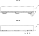
- FIG. 4 is a back surface plan view illustrating a solar cell according to an example useful for understanding the present invention.
- the insulating layer 40 is not shown in FIG. 4 .
- the first conductive type area 32 may include a first stem portion 32a formed along a first edge (upper edge in the drawing) of the semiconductor substrate 10 and a plurality of first branch portions 32b which extend from the first stem portion 32a toward a second edge (lower edge in the drawing) opposite to the first edge.
- the plurality of first branch portions 32b are aligned to be parallel to each other to have a shape of a stripe pattern.
- the second conductive type area 34 may include a second stem portion 34a formed along the second edge of the semiconductor substrate 110 and a plurality of second branch portions 32b which extend between the first branch portions 32b toward the first edge from the second stem portion 34a.
- the plurality of second branch portions 34b are aligned to be parallel to each other to have a shape of a stripe pattern.
- the first branch portions 32b of the first conductive type area 32 and the second branch portions 34b of the second conductive type area 34 may be alternately disposed. Though this configuration, a junction area can be increased and carriers can be entirely collected.
- the barrier area 36 may be formed between the first conductive type area 32 and the second conductive type area 34.
- an area of the first conductive type area 32 may be smaller than an area of the second conductive type area 34.
- the area of the first and second conductive type areas 32 and 34 can be controlled by changing the first and second stem portions 32a and 34a and/or the first and second branch portions 32b and 34b of the first and second conductive type areas 32 and 34.
- the first electrode 42 includes a stem portion 42a formed in a region corresponding to the first stem portion 32a of the first conductive type area 32, and a branch portion 42b formed in a region corresponding to the branch portion 32b of the first conductive type area 32.
- the second electrode 44 may include a stem portion 44a in a region corresponding to the second stem portion 34a of the second conductive type area 34, and a branch portion 44b formed in a region corresponding to the branch portion 34b of the second conductive type area 34, but the present disclosure is not limited thereto and the first electrode 42 and the second electrode 44 may have a variety of plane shapes.
- the first conductive type area has the first stem portion 32a
- the second conductive type area has the second stem portion 34a
- the first electrode 42 has the stem portion 42a
- the second electrode 44 has the stem portion 44a.
- the present disclosure is not limited thereto, and the first and second stem portions 32a and 34a, and the stem portions 42a and 44a are not necessary. Therefore, the first and/or second stem portions 32a and 34a, and/or the stem portions 42a and 44a may be not formed or may be not included.
- each of the first and second conductive type areas 32 and 34 consisting of the first and second branch portions 32b and 34b has a stripe pattern
- the barrier area 36 has a shape of a stripe pattern between the branch portion 32b of the first conductive type area 32 and the branch portion 32b of the second conductive type area 34.
- a ratio of a total area of the first conductive type area 32 to a total area of the solar cell 100 may be 0.5% to 49% (more preferably 20% to 40%).
- the ratio of the total area of the first conductive type area 32 is less than 0.5%, contact between the first conductive type area 32 and the first electrode 42 is not accurately formed and contact resistance between the first conductive type area 32 and the first electrode 42 may thus be increased.
- the area ratio exceeds 49%, the area of the first conductive type area 32 is decreased and efficiency of the solar cell 100 is thus deteriorated, as described above.
- the area ratio is preferably 20% to 40% in consideration of efficiency of the solar cell.
- the width of each of the first branch portions 32b having the stripe pattern may be 50 ⁇ m to 1,000 ⁇ m.
- the width of the first branch portions 32b is less than 50 ⁇ m, electrical connection between the first conductive type area 32 and the first electrode 42 may be not efficiently formed.
- the width exceeds 1,000 ⁇ m an area of the second conductive type area 34 is decreased or a distance between the first conductive type areas 32 is increased.
- the width of each of the first branch portions 32b 32 may be 100 ⁇ m to 500 ⁇ m.
- FIG. 5 is a sectional view illustrating a solar cell according to, another example useful for understanding the present invention.
- the semiconductor substrate 10 includes only the base area 110 and does not include an additional front surface field layer (represented by reference numeral "120" in FIG. 1 , the same will be applied below). Instead, a field effect-forming layer 52 which contacts the base area 110 of the semiconductor substrate 10 and has a fixed charge is formed. Similar to the front surface field layer 112, the field effect-forming layer 52 generates a certain field effect and thereby prevents surface recombination.
- the field effect-forming layer 52 may be composed of aluminum oxide having a negative charge, or silicon oxide or silicon nitride having a positive charge or the like.
- an additional anti-reflective film represented by reference numeral "50" in FIG. 1 ) may be further formed on the field effect-forming layer 52.
- the semiconductor substrate 10 does not include an additional doping area and includes only a base area 110.
- a process of forming the additional doping area is eliminated and the overall process is thus simplified.
- deterioration in properties of the solar cell 100 caused by damage to the semiconductor substrate 10 can be prevented.
- an amount of fixed charges of the field effect-forming layer 52 is for example 1 X 10 12 /cm 2 to 9 X 10 13 /cm 2 .
- the amount of the fixed charges is a level enabling generation of the field effect in the semiconductor substrate 10 not including the doping area. More specifically, in consideration of the field effect, the amount of fixed charges may be 1 X 10 12 /cm 2 to 1 X 10 13 /cm 2 , but the present invention is not limited thereto and the amount of fixed charges may be varied.
- the base area 110 not including the doping area may have a specific resistance of 0.5 ohm ⁇ cm to 20 ohm ⁇ cm (for example, 1 ohm ⁇ cm to 15 ohm ⁇ cm) .
- the semiconductor substrate 10 may have a specific resistance of 0.5 ohm ⁇ cm to 20 ohm ⁇ cm (for example, 1 ohm ⁇ cm to 15 ohm ⁇ cm) .
- this specific resistance range is given as an example of a case when the semiconductor substrate 10 includes an n-type base area 110 using phosphorous (P) as an impurity and may be changed according to conductive type, impurity type or the like.
Landscapes
- Photovoltaic Devices (AREA)
- Engineering & Computer Science (AREA)
- Life Sciences & Earth Sciences (AREA)
- Sustainable Energy (AREA)
- Sustainable Development (AREA)
- Manufacturing & Machinery (AREA)
Claims (13)
- Verfahren zum Herstellen einer Solarzelle (100), umfassend:- Ausbilden einer Tunnelschicht (20) auf einer Oberfläche eines Halbleitersubstrats (110);- Ausbilden einer Halbleiterschicht (30) auf der Tunnelschicht (20); und- Dotieren der Halbleiterschicht (30) mit einem Dotierstoff einer ersten Leitfähigkeitsart und einem Dotierstoff einer zweiten Leitfähigkeitsart, um einen Bereich (32) der ersten Leitfähigkeitsart und einen Bereich (34) der zweiten Leitfähigkeitsart auszubilden, die über einen Barrierebereich (36) voneinander getrennt sind, wobei das Dotieren der Halbleiterschicht (30) umfasst:- Ausbilden einer ersten Dotierungsschicht (322), die den Dotierstoff der ersten Leitfähigkeitsart einschließt, auf der Halbleiterschicht in einem Bereich, der dem Bereich (32) der ersten Leitfähigkeitsart entspricht;- Ausbilden einer undotierten Schicht (362) auf der ersten Dotierungsschicht (322) und auf einem Abschnitt der Halbleiterschicht, der an die erste Dotierungsschicht angrenzt;- Ausbilden einer zweiten Dotierungsschicht (342), die den Dotierstoff der zweiten Leitfähigkeitsart einschließt, auf der undotierten Schicht (362) und der Halbleiterschicht (30), um die undotierte Schicht (362) und die Halbleiterschicht (30) vollständig zu bedecken; und- Diffundieren des Dotierstoffs der ersten Leitfähigkeitsart und des Dotierstoffs der zweiten Leitfähigkeitsart in die Halbleiterschicht, um gleichzeitig den Bereich (32) der ersten Leitfähigkeitsart, den Bereich (34) der zweiten Leitfähigkeitsart und den Barrierebereich (36) auszubilden,- wobei, bei der Diffusion, ein Abschnitt der Halbleiterschicht (30), in den der Dotierstoff der ersten Leitfähigkeitsart diffundiert wird, den Bereich (32) der ersten Leitfähigkeitsart ausbildet, ein Abschnitt der Halbleiterschicht, in den der Dotierstoff der zweiten Leitfähigkeitsart diffundiert wird, den Bereich (34) der zweiten Leitfähigkeitsart ausbildet und ein undotierter Abschnitt zwischen dem Bereich der ersten Leitfähigkeitsart und dem Bereich der zweiten Leitfähigkeitsart den Barrierebereich (36) ausbildet.
- Verfahren nach Anspruch 1,- wobei eine der ersten und der zweiten Dotierungsschicht Borsilikatglas umfasst und die andere Phosphorsilikatglas umfasst.
- Verfahren nach Anspruch 1 oder 2, umfassend:- Texturieren einer vorderen Oberfläche des Halbleitersubstrats (110) vor dem Ausbilden der Tunnelschicht (20).
- Verfahren nach Anspruch 3,- wobei das Texturieren ein Nass- oder Trockentexturieren ist.
- Verfahren nach einem der vorstehenden Ansprüche,- wobei die Tunnelschicht (20) und/oder die Halbleiterschicht (30) durch thermisches Wachstum oder Abscheidung ausgebildet werden.
- Verfahren nach einem der vorstehenden Ansprüche,- wobei die erste Dotierungsschicht (322) eine Vielzahl von Dotierungsabschnitten einschließt, die einer Vielzahl von Bereichen (32) der ersten Leitfähigkeitsart entsprechen.
- Verfahren nach einem der vorstehenden Ansprüche,- wobei die erste Dotierschicht (322) durch Verwenden einer Maske oder durch ein Tintenstrahlverfahren oder durch einen Siebdruck oder durch ein vollständiges Ausbilden eines Materials auf der Halbleiterschicht (30) und Entfernen von Regionen, in denen die Bereiche (32) der ersten Leitfähigkeitsart nicht ausgebildet sind, unter Verwendung einer Ätzlösung oder einer Ätzpaste ausgebildet wird.
- Verfahren nach einem der vorstehenden Ansprüche,- wobei die undotierte Schicht (362) durch Verwenden einer Maske auf der Halbleiterschicht (30) oder durch das Tintenstrahlverfahren oder durch den Siebdruck oder durch das vollständige Ausbilden eines Materials zum Ausbilden der undotierten Schicht (362) über der ersten Dotierschicht (322) und der Halbleiterschicht (30) und Entfernen unerwünschter Regionen unter Verwendung einer Ätzlösung oder einer Ätzpaste ausgebildet wird.
- Verfahren nach einem der vorstehenden Ansprüche,- wobei die Diffusion durch eine thermische Behandlung durchgeführt wird.
- Verfahren nach einem der vorstehenden Ansprüche,umfassend:- Entfernen der ersten Dotierschicht (322), der undotierten Schicht (362) und der zweiten Dotierschicht (342) nach der Diffusion.
- Verfahren nach Anspruch 10, umfassend:- Ausbilden einer Isolierschicht (40) auf den Bereichen (32, 34) der ersten und der zweiten Leitfähigkeitsart und dem Barrierebereich (36) nach dem Entfernen der ersten Dotierungsschicht (322), der undotierten Schicht (362) und der zweiten Dotierungsschicht (342).
- Verfahren nach Anspruch 11, umfassend:- Ausbilden einer Feldschicht (120) der vorderen Oberfläche und eines Antireflexionsfilms (50) auf der vorderen Oberfläche des Halbleitersubstrats (10).
- Verfahren nach Anspruch 12, umfassend:- Ausbilden von Öffnungen (402, 404) durch Freilegen der Bereiche (32, 34) der ersten und der zweiten Leitfähigkeitsart, und- elektrisches Verbinden der ersten und der zweiten Elektroden (42, 44) mit den Bereichen (32, 34) der ersten beziehungsweise der zweiten Leitfähigkeitsart.
Priority Applications (1)
| Application Number | Priority Date | Filing Date | Title |
|---|---|---|---|
| EP24188663.9A EP4421886A3 (de) | 2013-04-23 | 2014-04-22 | Verfahren zur herstellung einer solarzelle |
Applications Claiming Priority (1)
| Application Number | Priority Date | Filing Date | Title |
|---|---|---|---|
| KR1020130044982A KR101613843B1 (ko) | 2013-04-23 | 2013-04-23 | 태양 전지 및 이의 제조 방법 |
Related Child Applications (2)
| Application Number | Title | Priority Date | Filing Date |
|---|---|---|---|
| EP24188663.9A Division EP4421886A3 (de) | 2013-04-23 | 2014-04-22 | Verfahren zur herstellung einer solarzelle |
| EP24188663.9A Division-Into EP4421886A3 (de) | 2013-04-23 | 2014-04-22 | Verfahren zur herstellung einer solarzelle |
Publications (3)
| Publication Number | Publication Date |
|---|---|
| EP2797124A1 EP2797124A1 (de) | 2014-10-29 |
| EP2797124B1 true EP2797124B1 (de) | 2024-09-25 |
| EP2797124C0 EP2797124C0 (de) | 2024-09-25 |
Family
ID=50542775
Family Applications (2)
| Application Number | Title | Priority Date | Filing Date |
|---|---|---|---|
| EP14001446.5A Active EP2797124B1 (de) | 2013-04-23 | 2014-04-22 | Verfahren zur Herstellung einer Solarzelle |
| EP24188663.9A Pending EP4421886A3 (de) | 2013-04-23 | 2014-04-22 | Verfahren zur herstellung einer solarzelle |
Family Applications After (1)
| Application Number | Title | Priority Date | Filing Date |
|---|---|---|---|
| EP24188663.9A Pending EP4421886A3 (de) | 2013-04-23 | 2014-04-22 | Verfahren zur herstellung einer solarzelle |
Country Status (5)
| Country | Link |
|---|---|
| US (1) | US10854764B2 (de) |
| EP (2) | EP2797124B1 (de) |
| KR (1) | KR101613843B1 (de) |
| CN (1) | CN104124302B (de) |
| ES (1) | ES3002457T3 (de) |
Families Citing this family (25)
| Publication number | Priority date | Publication date | Assignee | Title |
|---|---|---|---|---|
| NL2013722B1 (en) * | 2014-10-31 | 2016-10-04 | Univ Delft Tech | Back side contacted wafer-based solar cells with in-situ doped crystallized thin-film silicon and/or silicon oxide regions. |
| KR20160052270A (ko) * | 2014-11-04 | 2016-05-12 | 엘지전자 주식회사 | 태양 전지 |
| KR102286289B1 (ko) * | 2014-11-26 | 2021-08-04 | 엘지전자 주식회사 | 태양 전지 |
| JP6219913B2 (ja) | 2014-11-28 | 2017-10-25 | エルジー エレクトロニクス インコーポレイティド | 太陽電池及びその製造方法 |
| KR20160064692A (ko) * | 2014-11-28 | 2016-06-08 | 엘지전자 주식회사 | 태양 전지 및 그 제조 방법 |
| KR20160084261A (ko) * | 2015-01-05 | 2016-07-13 | 엘지전자 주식회사 | 태양 전지 및 이의 제조 방법 |
| US10566483B2 (en) * | 2015-03-17 | 2020-02-18 | Lg Electronics Inc. | Solar cell |
| EP3093889B8 (de) * | 2015-05-13 | 2024-05-22 | Trina Solar Co., Ltd | Solarzelle und verfahren zur herstellung davon |
| DE102015107842B3 (de) * | 2015-05-19 | 2016-10-27 | Institut Für Solarenergieforschung Gmbh | Verfahren zum Herstellen einer Solarzelle mit oxidierten Zwischenbereichen zwischen Poly-Silizium-Kontakten |
| WO2016208219A1 (ja) * | 2015-06-25 | 2016-12-29 | シャープ株式会社 | 光電変換装置 |
| NL2015533B1 (en) * | 2015-09-30 | 2017-04-20 | Tempress Ip B V | Method of manufacturing of a solar cell and solar cell thus obtained. |
| EP3151289A1 (de) * | 2015-10-01 | 2017-04-05 | LG Electronics Inc. | Solarzelle |
| KR102547806B1 (ko) * | 2016-04-15 | 2023-06-28 | 오씨아이 주식회사 | 후면접합 실리콘 태양전지 제조방법 |
| KR101870222B1 (ko) * | 2016-09-30 | 2018-07-20 | 엘지전자 주식회사 | 태양 전지 및 그의 제조 방법 |
| US11201253B2 (en) * | 2016-11-15 | 2021-12-14 | Shin-Etsu Chemical Co., Ltd. | High photovoltaic-conversion efficiency solar cell, method for manufacturing the same, solar cell module, and photovoltaic power generation system |
| KR102005439B1 (ko) * | 2016-11-23 | 2019-07-30 | 엘지전자 주식회사 | 태양 전지 제조 방법 |
| NL2017872B1 (en) * | 2016-11-25 | 2018-06-08 | Stichting Energieonderzoek Centrum Nederland | Photovoltaic cell with passivating contact |
| NL2019634B1 (en) | 2017-09-27 | 2019-04-03 | Univ Delft Tech | Solar cells with transparent contacts based on poly-silicon-oxide |
| CN107731957A (zh) * | 2017-09-29 | 2018-02-23 | 浙江晶科能源有限公司 | 一种太阳能电池的制备方法 |
| CN108963005B (zh) * | 2018-07-05 | 2021-01-26 | 深圳市拉普拉斯能源技术有限公司 | 一种新型复合结构全背面异质结太阳电池及制备方法 |
| WO2020071083A1 (ja) * | 2018-10-02 | 2020-04-09 | 株式会社カネカ | 太陽電池デバイスおよび太陽電池モジュール |
| CN112466961B (zh) | 2020-11-19 | 2024-05-10 | 晶科绿能(上海)管理有限公司 | 太阳能电池及其制造方法 |
| CN115985981B (zh) * | 2023-02-22 | 2023-06-20 | 浙江晶科能源有限公司 | 太阳能电池及其制备方法、光伏组件 |
| CN116314361B (zh) | 2023-03-31 | 2025-06-13 | 天合光能股份有限公司 | 太阳电池及太阳电池的制备方法 |
| CN117352567A (zh) * | 2023-09-28 | 2024-01-05 | 浙江晶科能源有限公司 | 太阳能电池及光伏组件 |
Citations (1)
| Publication number | Priority date | Publication date | Assignee | Title |
|---|---|---|---|---|
| US20120199183A1 (en) * | 2011-02-08 | 2012-08-09 | Min Seok Oh | Solar cell and method of manufacturing the same |
Family Cites Families (32)
| Publication number | Priority date | Publication date | Assignee | Title |
|---|---|---|---|---|
| US4315097A (en) * | 1980-10-27 | 1982-02-09 | Mcdonnell Douglas Corporation | Back contacted MIS photovoltaic cell |
| US5057439A (en) * | 1990-02-12 | 1991-10-15 | Electric Power Research Institute | Method of fabricating polysilicon emitters for solar cells |
| US20060130891A1 (en) * | 2004-10-29 | 2006-06-22 | Carlson David E | Back-contact photovoltaic cells |
| US7468485B1 (en) * | 2005-08-11 | 2008-12-23 | Sunpower Corporation | Back side contact solar cell with doped polysilicon regions |
| US8008575B2 (en) * | 2006-07-24 | 2011-08-30 | Sunpower Corporation | Solar cell with reduced base diffusion area |
| WO2008115814A2 (en) * | 2007-03-16 | 2008-09-25 | Bp Corporation North America Inc. | Solar cells |
| WO2009025147A1 (ja) * | 2007-08-23 | 2009-02-26 | Sharp Kabushiki Kaisha | 裏面接合型太陽電池、配線基板付き裏面接合型太陽電池、太陽電池ストリングおよび太陽電池モジュール |
| US7727866B2 (en) * | 2008-03-05 | 2010-06-01 | Varian Semiconductor Equipment Associates, Inc. | Use of chained implants in solar cells |
| JP2011517120A (ja) * | 2008-04-09 | 2011-05-26 | アプライド マテリアルズ インコーポレイテッド | ポリシリコンエミッタ太陽電池用簡易裏面接触 |
| US20090293948A1 (en) * | 2008-05-28 | 2009-12-03 | Stichting Energieonderzoek Centrum Nederland | Method of manufacturing an amorphous/crystalline silicon heterojunction solar cell |
| US7851698B2 (en) | 2008-06-12 | 2010-12-14 | Sunpower Corporation | Trench process and structure for backside contact solar cells with polysilicon doped regions |
| TWI390756B (zh) * | 2008-07-16 | 2013-03-21 | Applied Materials Inc | 使用摻質層遮罩之混合異接面太陽能電池製造 |
| CN102132422A (zh) * | 2008-08-27 | 2011-07-20 | 应用材料股份有限公司 | 利用印刷介电阻障的背接触太阳能电池 |
| US7951696B2 (en) * | 2008-09-30 | 2011-05-31 | Honeywell International Inc. | Methods for simultaneously forming N-type and P-type doped regions using non-contact printing processes |
| US8242354B2 (en) * | 2008-12-04 | 2012-08-14 | Sunpower Corporation | Backside contact solar cell with formed polysilicon doped regions |
| KR101142861B1 (ko) * | 2009-02-04 | 2012-05-08 | 엘지전자 주식회사 | 태양 전지 및 그 제조 방법 |
| KR101135591B1 (ko) * | 2009-03-11 | 2012-04-19 | 엘지전자 주식회사 | 태양 전지 및 태양 전지 모듈 |
| US20100229928A1 (en) * | 2009-03-12 | 2010-09-16 | Twin Creeks Technologies, Inc. | Back-contact photovoltaic cell comprising a thin lamina having a superstrate receiver element |
| US20110027463A1 (en) * | 2009-06-16 | 2011-02-03 | Varian Semiconductor Equipment Associates, Inc. | Workpiece handling system |
| CN102074599B (zh) * | 2009-09-07 | 2014-10-29 | Lg电子株式会社 | 太阳能电池及其制造方法 |
| US20110073175A1 (en) * | 2009-09-29 | 2011-03-31 | Twin Creeks Technologies, Inc. | Photovoltaic cell comprising a thin lamina having emitter formed at light-facing and back surfaces |
| US8324015B2 (en) * | 2009-12-01 | 2012-12-04 | Sunpower Corporation | Solar cell contact formation using laser ablation |
| US8492253B2 (en) * | 2010-12-02 | 2013-07-23 | Sunpower Corporation | Method of forming contacts for a back-contact solar cell |
| US8450051B2 (en) * | 2010-12-20 | 2013-05-28 | Varian Semiconductor Equipment Associates, Inc. | Use of patterned UV source for photolithography |
| US20120167978A1 (en) * | 2011-01-03 | 2012-07-05 | Lg Electronics Inc. | Solar cell and method for manufacturing the same |
| US8242005B1 (en) * | 2011-01-24 | 2012-08-14 | Varian Semiconductor Equipment Associates, Inc. | Using multiple masks to form independent features on a workpiece |
| US8486746B2 (en) | 2011-03-29 | 2013-07-16 | Sunpower Corporation | Thin silicon solar cell and method of manufacture |
| GB2491209B (en) * | 2011-05-27 | 2013-08-21 | Renewable Energy Corp Asa | Solar cell and method for producing same |
| US8658458B2 (en) * | 2011-06-15 | 2014-02-25 | Varian Semiconductor Equipment Associates, Inc. | Patterned doping for polysilicon emitter solar cells |
| US8697559B2 (en) * | 2011-07-07 | 2014-04-15 | Varian Semiconductor Equipment Associates, Inc. | Use of ion beam tails to manufacture a workpiece |
| US8785233B2 (en) * | 2012-12-19 | 2014-07-22 | Sunpower Corporation | Solar cell emitter region fabrication using silicon nano-particles |
| EP2782144B1 (de) * | 2013-03-19 | 2019-05-15 | IMEC vzw | Verfahren zur Herstellung ineinandergreifender Ruhekontakt-Photovoltaikzellen mit Heteroübergang |
-
2013
- 2013-04-23 KR KR1020130044982A patent/KR101613843B1/ko active Active
-
2014
- 2014-04-22 US US14/258,638 patent/US10854764B2/en active Active
- 2014-04-22 EP EP14001446.5A patent/EP2797124B1/de active Active
- 2014-04-22 ES ES14001446T patent/ES3002457T3/es active Active
- 2014-04-22 EP EP24188663.9A patent/EP4421886A3/de active Pending
- 2014-04-23 CN CN201410165536.9A patent/CN104124302B/zh active Active
Patent Citations (1)
| Publication number | Priority date | Publication date | Assignee | Title |
|---|---|---|---|---|
| US20120199183A1 (en) * | 2011-02-08 | 2012-08-09 | Min Seok Oh | Solar cell and method of manufacturing the same |
Also Published As
| Publication number | Publication date |
|---|---|
| ES3002457T3 (en) | 2025-03-07 |
| KR101613843B1 (ko) | 2016-04-20 |
| CN104124302B (zh) | 2017-04-12 |
| EP4421886A3 (de) | 2024-11-27 |
| US20140311567A1 (en) | 2014-10-23 |
| CN104124302A (zh) | 2014-10-29 |
| EP2797124A1 (de) | 2014-10-29 |
| EP4421886A2 (de) | 2024-08-28 |
| EP2797124C0 (de) | 2024-09-25 |
| KR20140126872A (ko) | 2014-11-03 |
| US10854764B2 (en) | 2020-12-01 |
Similar Documents
| Publication | Publication Date | Title |
|---|---|---|
| EP2797124B1 (de) | Verfahren zur Herstellung einer Solarzelle | |
| US20230023777A1 (en) | Solar cell | |
| EP2804219B1 (de) | Solarzelle und verfahren zu ihrer herstellung | |
| EP2822041B1 (de) | Solarzelle und Verfahren zu ihrer Herstellung | |
| CN106159008B (zh) | 太阳能电池及其制造方法 | |
| KR20150049211A (ko) | 태양 전지 및 이의 제조 방법 | |
| KR101755624B1 (ko) | 태양 전지의 제조 방법 | |
| KR102132741B1 (ko) | 태양 전지 및 이의 제조 방법 | |
| KR20160034062A (ko) | 태양 전지 및 이의 제조 방법 | |
| KR20160063010A (ko) | 태양 전지 및 이의 제조 방법 | |
| KR101199649B1 (ko) | 국부화 에미터 태양전지 및 그 제조 방법 | |
| KR102082880B1 (ko) | 태양 전지의 제조 방법 | |
| KR20160111624A (ko) | 태양 전지 및 이의 제조 방법 | |
| KR20120021860A (ko) | 태양전지 제조 방법 |
Legal Events
| Date | Code | Title | Description |
|---|---|---|---|
| PUAI | Public reference made under article 153(3) epc to a published international application that has entered the european phase |
Free format text: ORIGINAL CODE: 0009012 |
|
| 17P | Request for examination filed |
Effective date: 20140422 |
|
| AK | Designated contracting states |
Kind code of ref document: A1 Designated state(s): AL AT BE BG CH CY CZ DE DK EE ES FI FR GB GR HR HU IE IS IT LI LT LU LV MC MK MT NL NO PL PT RO RS SE SI SK SM TR |
|
| AX | Request for extension of the european patent |
Extension state: BA ME |
|
| STAA | Information on the status of an ep patent application or granted ep patent |
Free format text: STATUS: EXAMINATION IS IN PROGRESS |
|
| 17Q | First examination report despatched |
Effective date: 20190513 |
|
| RAP1 | Party data changed (applicant data changed or rights of an application transferred) |
Owner name: SHANGRAO JINKO SOLAR TECHNOLOGY DEVELOPMENT CO., LTD |
|
| RAP3 | Party data changed (applicant data changed or rights of an application transferred) |
Owner name: SHANGRAO XINYUAN YUEDONG TECHNOLOGY DEVELOPMENT CO. LTD |
|
| GRAP | Despatch of communication of intention to grant a patent |
Free format text: ORIGINAL CODE: EPIDOSNIGR1 |
|
| STAA | Information on the status of an ep patent application or granted ep patent |
Free format text: STATUS: GRANT OF PATENT IS INTENDED |
|
| RAP1 | Party data changed (applicant data changed or rights of an application transferred) |
Owner name: TRINA SOLAR CO., LTD |
|
| INTG | Intention to grant announced |
Effective date: 20240418 |
|
| GRAS | Grant fee paid |
Free format text: ORIGINAL CODE: EPIDOSNIGR3 |
|
| GRAA | (expected) grant |
Free format text: ORIGINAL CODE: 0009210 |
|
| STAA | Information on the status of an ep patent application or granted ep patent |
Free format text: STATUS: THE PATENT HAS BEEN GRANTED |
|
| AK | Designated contracting states |
Kind code of ref document: B1 Designated state(s): AL AT BE BG CH CY CZ DE DK EE ES FI FR GB GR HR HU IE IS IT LI LT LU LV MC MK MT NL NO PL PT RO RS SE SI SK SM TR |
|
| REG | Reference to a national code |
Ref country code: GB Ref legal event code: FG4D |
|
| REG | Reference to a national code |
Ref country code: CH Ref legal event code: EP |
|
| REG | Reference to a national code |
Ref country code: DE Ref legal event code: R096 Ref document number: 602014090904 Country of ref document: DE |
|
| REG | Reference to a national code |
Ref country code: IE Ref legal event code: FG4D |
|
| U01 | Request for unitary effect filed |
Effective date: 20241003 |
|
| U07 | Unitary effect registered |
Designated state(s): AT BE BG DE DK EE FI FR IT LT LU LV MT NL PT RO SE SI Effective date: 20241016 |
|
| PG25 | Lapsed in a contracting state [announced via postgrant information from national office to epo] |
Ref country code: NO Free format text: LAPSE BECAUSE OF FAILURE TO SUBMIT A TRANSLATION OF THE DESCRIPTION OR TO PAY THE FEE WITHIN THE PRESCRIBED TIME-LIMIT Effective date: 20241225 |
|
| PG25 | Lapsed in a contracting state [announced via postgrant information from national office to epo] |
Ref country code: GR Free format text: LAPSE BECAUSE OF FAILURE TO SUBMIT A TRANSLATION OF THE DESCRIPTION OR TO PAY THE FEE WITHIN THE PRESCRIBED TIME-LIMIT Effective date: 20241226 |
|
| PG25 | Lapsed in a contracting state [announced via postgrant information from national office to epo] |
Ref country code: RS Free format text: LAPSE BECAUSE OF FAILURE TO SUBMIT A TRANSLATION OF THE DESCRIPTION OR TO PAY THE FEE WITHIN THE PRESCRIBED TIME-LIMIT Effective date: 20241225 |
|
| PG25 | Lapsed in a contracting state [announced via postgrant information from national office to epo] |
Ref country code: RS Free format text: LAPSE BECAUSE OF FAILURE TO SUBMIT A TRANSLATION OF THE DESCRIPTION OR TO PAY THE FEE WITHIN THE PRESCRIBED TIME-LIMIT Effective date: 20241225 Ref country code: NO Free format text: LAPSE BECAUSE OF FAILURE TO SUBMIT A TRANSLATION OF THE DESCRIPTION OR TO PAY THE FEE WITHIN THE PRESCRIBED TIME-LIMIT Effective date: 20241225 Ref country code: GR Free format text: LAPSE BECAUSE OF FAILURE TO SUBMIT A TRANSLATION OF THE DESCRIPTION OR TO PAY THE FEE WITHIN THE PRESCRIBED TIME-LIMIT Effective date: 20241226 |
|
| REG | Reference to a national code |
Ref country code: ES Ref legal event code: FG2A Ref document number: 3002457 Country of ref document: ES Kind code of ref document: T3 Effective date: 20250307 |
|
| U20 | Renewal fee for the european patent with unitary effect paid |
Year of fee payment: 12 Effective date: 20250205 |
|
| PG25 | Lapsed in a contracting state [announced via postgrant information from national office to epo] |
Ref country code: IS Free format text: LAPSE BECAUSE OF FAILURE TO SUBMIT A TRANSLATION OF THE DESCRIPTION OR TO PAY THE FEE WITHIN THE PRESCRIBED TIME-LIMIT Effective date: 20250125 |
|
| PG25 | Lapsed in a contracting state [announced via postgrant information from national office to epo] |
Ref country code: SM Free format text: LAPSE BECAUSE OF FAILURE TO SUBMIT A TRANSLATION OF THE DESCRIPTION OR TO PAY THE FEE WITHIN THE PRESCRIBED TIME-LIMIT Effective date: 20240925 |
|
| PG25 | Lapsed in a contracting state [announced via postgrant information from national office to epo] |
Ref country code: PL Free format text: LAPSE BECAUSE OF FAILURE TO SUBMIT A TRANSLATION OF THE DESCRIPTION OR TO PAY THE FEE WITHIN THE PRESCRIBED TIME-LIMIT Effective date: 20240925 Ref country code: CZ Free format text: LAPSE BECAUSE OF FAILURE TO SUBMIT A TRANSLATION OF THE DESCRIPTION OR TO PAY THE FEE WITHIN THE PRESCRIBED TIME-LIMIT Effective date: 20240925 |
|
| PG25 | Lapsed in a contracting state [announced via postgrant information from national office to epo] |
Ref country code: SK Free format text: LAPSE BECAUSE OF FAILURE TO SUBMIT A TRANSLATION OF THE DESCRIPTION OR TO PAY THE FEE WITHIN THE PRESCRIBED TIME-LIMIT Effective date: 20240925 |
|
| PGFP | Annual fee paid to national office [announced via postgrant information from national office to epo] |
Ref country code: GB Payment date: 20250224 Year of fee payment: 12 |
|
| PGFP | Annual fee paid to national office [announced via postgrant information from national office to epo] |
Ref country code: ES Payment date: 20250519 Year of fee payment: 12 |
|
| PLBE | No opposition filed within time limit |
Free format text: ORIGINAL CODE: 0009261 |
|
| STAA | Information on the status of an ep patent application or granted ep patent |
Free format text: STATUS: NO OPPOSITION FILED WITHIN TIME LIMIT |
|
| 26N | No opposition filed |
Effective date: 20250626 |
|
| REG | Reference to a national code |
Ref country code: CH Ref legal event code: H13 Free format text: ST27 STATUS EVENT CODE: U-0-0-H10-H13 (AS PROVIDED BY THE NATIONAL OFFICE) Effective date: 20251125 |