EP2782150A2 - Light emitting device package and backlight including same - Google Patents
Light emitting device package and backlight including same Download PDFInfo
- Publication number
- EP2782150A2 EP2782150A2 EP12850417.2A EP12850417A EP2782150A2 EP 2782150 A2 EP2782150 A2 EP 2782150A2 EP 12850417 A EP12850417 A EP 12850417A EP 2782150 A2 EP2782150 A2 EP 2782150A2
- Authority
- EP
- European Patent Office
- Prior art keywords
- light emitting
- emitting element
- molded material
- reflection structure
- opening
- Prior art date
- Legal status (The legal status is an assumption and is not a legal conclusion. Google has not performed a legal analysis and makes no representation as to the accuracy of the status listed.)
- Granted
Links
Images





Classifications
-
- H—ELECTRICITY
- H10—SEMICONDUCTOR DEVICES; ELECTRIC SOLID-STATE DEVICES NOT OTHERWISE PROVIDED FOR
- H10H—INORGANIC LIGHT-EMITTING SEMICONDUCTOR DEVICES HAVING POTENTIAL BARRIERS
- H10H20/00—Individual inorganic light-emitting semiconductor devices having potential barriers, e.g. light-emitting diodes [LED]
- H10H20/80—Constructional details
- H10H20/85—Packages
- H10H20/857—Interconnections, e.g. lead-frames, bond wires or solder balls
-
- H—ELECTRICITY
- H10—SEMICONDUCTOR DEVICES; ELECTRIC SOLID-STATE DEVICES NOT OTHERWISE PROVIDED FOR
- H10H—INORGANIC LIGHT-EMITTING SEMICONDUCTOR DEVICES HAVING POTENTIAL BARRIERS
- H10H20/00—Individual inorganic light-emitting semiconductor devices having potential barriers, e.g. light-emitting diodes [LED]
- H10H20/80—Constructional details
- H10H20/85—Packages
- H10H20/8506—Containers
-
- H—ELECTRICITY
- H10—SEMICONDUCTOR DEVICES; ELECTRIC SOLID-STATE DEVICES NOT OTHERWISE PROVIDED FOR
- H10H—INORGANIC LIGHT-EMITTING SEMICONDUCTOR DEVICES HAVING POTENTIAL BARRIERS
- H10H20/00—Individual inorganic light-emitting semiconductor devices having potential barriers, e.g. light-emitting diodes [LED]
- H10H20/80—Constructional details
- H10H20/85—Packages
- H10H20/852—Encapsulations
- H10H20/853—Encapsulations characterised by their shape
-
- H—ELECTRICITY
- H10—SEMICONDUCTOR DEVICES; ELECTRIC SOLID-STATE DEVICES NOT OTHERWISE PROVIDED FOR
- H10H—INORGANIC LIGHT-EMITTING SEMICONDUCTOR DEVICES HAVING POTENTIAL BARRIERS
- H10H20/00—Individual inorganic light-emitting semiconductor devices having potential barriers, e.g. light-emitting diodes [LED]
- H10H20/80—Constructional details
- H10H20/85—Packages
- H10H20/855—Optical field-shaping means, e.g. lenses
- H10H20/856—Reflecting means
-
- G—PHYSICS
- G02—OPTICS
- G02B—OPTICAL ELEMENTS, SYSTEMS OR APPARATUS
- G02B6/00—Light guides; Structural details of arrangements comprising light guides and other optical elements, e.g. couplings
- G02B6/0001—Light guides; Structural details of arrangements comprising light guides and other optical elements, e.g. couplings specially adapted for lighting devices or systems
- G02B6/0011—Light guides; Structural details of arrangements comprising light guides and other optical elements, e.g. couplings specially adapted for lighting devices or systems the light guides being planar or of plate-like form
- G02B6/0013—Means for improving the coupling-in of light from the light source into the light guide
- G02B6/0023—Means for improving the coupling-in of light from the light source into the light guide provided by one optical element, or plurality thereof, placed between the light guide and the light source, or around the light source
- G02B6/0031—Reflecting element, sheet or layer
-
- G—PHYSICS
- G02—OPTICS
- G02B—OPTICAL ELEMENTS, SYSTEMS OR APPARATUS
- G02B6/00—Light guides; Structural details of arrangements comprising light guides and other optical elements, e.g. couplings
- G02B6/0001—Light guides; Structural details of arrangements comprising light guides and other optical elements, e.g. couplings specially adapted for lighting devices or systems
- G02B6/0011—Light guides; Structural details of arrangements comprising light guides and other optical elements, e.g. couplings specially adapted for lighting devices or systems the light guides being planar or of plate-like form
- G02B6/0066—Light guides; Structural details of arrangements comprising light guides and other optical elements, e.g. couplings specially adapted for lighting devices or systems the light guides being planar or of plate-like form characterised by the light source being coupled to the light guide
- G02B6/0073—Light emitting diode [LED]
-
- G—PHYSICS
- G02—OPTICS
- G02B—OPTICAL ELEMENTS, SYSTEMS OR APPARATUS
- G02B6/00—Light guides; Structural details of arrangements comprising light guides and other optical elements, e.g. couplings
- G02B6/0001—Light guides; Structural details of arrangements comprising light guides and other optical elements, e.g. couplings specially adapted for lighting devices or systems
- G02B6/0011—Light guides; Structural details of arrangements comprising light guides and other optical elements, e.g. couplings specially adapted for lighting devices or systems the light guides being planar or of plate-like form
- G02B6/0081—Mechanical or electrical aspects of the light guide and light source in the lighting device peculiar to the adaptation to planar light guides, e.g. concerning packaging
- G02B6/0085—Means for removing heat created by the light source from the package
-
- G—PHYSICS
- G02—OPTICS
- G02F—OPTICAL DEVICES OR ARRANGEMENTS FOR THE CONTROL OF LIGHT BY MODIFICATION OF THE OPTICAL PROPERTIES OF THE MEDIA OF THE ELEMENTS INVOLVED THEREIN; NON-LINEAR OPTICS; FREQUENCY-CHANGING OF LIGHT; OPTICAL LOGIC ELEMENTS; OPTICAL ANALOGUE/DIGITAL CONVERTERS
- G02F1/00—Devices or arrangements for the control of the intensity, colour, phase, polarisation or direction of light arriving from an independent light source, e.g. switching, gating or modulating; Non-linear optics
- G02F1/01—Devices or arrangements for the control of the intensity, colour, phase, polarisation or direction of light arriving from an independent light source, e.g. switching, gating or modulating; Non-linear optics for the control of the intensity, phase, polarisation or colour
- G02F1/13—Devices or arrangements for the control of the intensity, colour, phase, polarisation or direction of light arriving from an independent light source, e.g. switching, gating or modulating; Non-linear optics for the control of the intensity, phase, polarisation or colour based on liquid crystals, e.g. single liquid crystal display cells
- G02F1/133—Constructional arrangements; Operation of liquid crystal cells; Circuit arrangements
- G02F1/1333—Constructional arrangements; Manufacturing methods
- G02F1/1335—Structural association of cells with optical devices, e.g. polarisers or reflectors
- G02F1/1336—Illuminating devices
- G02F1/133614—Illuminating devices using photoluminescence, e.g. phosphors illuminated by UV or blue light
-
- G—PHYSICS
- G02—OPTICS
- G02F—OPTICAL DEVICES OR ARRANGEMENTS FOR THE CONTROL OF LIGHT BY MODIFICATION OF THE OPTICAL PROPERTIES OF THE MEDIA OF THE ELEMENTS INVOLVED THEREIN; NON-LINEAR OPTICS; FREQUENCY-CHANGING OF LIGHT; OPTICAL LOGIC ELEMENTS; OPTICAL ANALOGUE/DIGITAL CONVERTERS
- G02F1/00—Devices or arrangements for the control of the intensity, colour, phase, polarisation or direction of light arriving from an independent light source, e.g. switching, gating or modulating; Non-linear optics
- G02F1/01—Devices or arrangements for the control of the intensity, colour, phase, polarisation or direction of light arriving from an independent light source, e.g. switching, gating or modulating; Non-linear optics for the control of the intensity, phase, polarisation or colour
- G02F1/13—Devices or arrangements for the control of the intensity, colour, phase, polarisation or direction of light arriving from an independent light source, e.g. switching, gating or modulating; Non-linear optics for the control of the intensity, phase, polarisation or colour based on liquid crystals, e.g. single liquid crystal display cells
- G02F1/133—Constructional arrangements; Operation of liquid crystal cells; Circuit arrangements
- G02F1/1333—Constructional arrangements; Manufacturing methods
- G02F1/1335—Structural association of cells with optical devices, e.g. polarisers or reflectors
- G02F1/1336—Illuminating devices
- G02F1/133615—Edge-illuminating devices, i.e. illuminating from the side
-
- H—ELECTRICITY
- H10—SEMICONDUCTOR DEVICES; ELECTRIC SOLID-STATE DEVICES NOT OTHERWISE PROVIDED FOR
- H10W—GENERIC PACKAGES, INTERCONNECTIONS, CONNECTORS OR OTHER CONSTRUCTIONAL DETAILS OF DEVICES COVERED BY CLASS H10
- H10W74/00—Encapsulations, e.g. protective coatings
-
- H—ELECTRICITY
- H10—SEMICONDUCTOR DEVICES; ELECTRIC SOLID-STATE DEVICES NOT OTHERWISE PROVIDED FOR
- H10W—GENERIC PACKAGES, INTERCONNECTIONS, CONNECTORS OR OTHER CONSTRUCTIONAL DETAILS OF DEVICES COVERED BY CLASS H10
- H10W90/00—Package configurations
- H10W90/701—Package configurations characterised by the relative positions of pads or connectors relative to package parts
- H10W90/751—Package configurations characterised by the relative positions of pads or connectors relative to package parts of bond wires
- H10W90/756—Package configurations characterised by the relative positions of pads or connectors relative to package parts of bond wires between a chip and a stacked lead frame, conducting package substrate or heat sink
Definitions
- the present invention relates to a light emitting element package and a backlight unit including the same. More particularly, the present invention relates to a light emitting element package having excellent heat radiation performance and high luminance, and a backlight unit including the same.
- a light emitting element is used as a light source of a backlight unit in an electronic device, e.g., display device.
- a light emitting element may be packaged in various ways before being connected to a backlight module and a backlight unit includes a packaged light emitting element.
- the light emitting element of the light emitting element package generates not only light but also a considerable amount of heat.
- the present invention has been made in an effort to solve various problems including the above problem, and provides a light emitting element package having excellent heat radiation performance and high luminance, and a backlight unit including the same.
- the scope of the present invention is not limited thereto.
- a light emitting element package including a lead frame, a light emitting element on the lead frame, a molded material combined with the lead frame and having an opening for emitting light generated by the light emitting element, and a reflection structure having an opening that corresponds to the opening of the molded material, and contacting the molded material.
- the reflection structure may include a supporting portion contacting the molded material and provided continuously or discretely along a circumference of the opening of the molded material, and a radial portion contacting the supporting portion and extending radially from the molded material relative to a direction along which light generated by the light emitting element emits.
- the molded material may include a supporting portion provided continuously or discretely along a circumference of the opening of the molded material, and the reflection structure may include a radial portion contacting the supporting portion and having a radial shape extending radially from the molded material relative to a direction along which light generated by the light emitting element emits.
- the molded material may include a supporting portion provided continuously or discretely along a circumference of the opening of the molded material, and the reflection structure may have a shape that corresponds to the supporting portion of the molded material and contact the molded material.
- Recesses or concave and convex portions may be provided on the molded material, and the reflection structure may be fitted into the recesses or concave and convex portions.
- the light emitting element package may further include an adhesive layer provided in at least part of a region between the molded material and the reflection structure to fix the reflection structure onto the molded material.
- the adhesive layer may have a first thickness in an area adjacent to the light emitting element and a second thickness in an area away from the light emitting element, and the first thickness may be greater than the second thickness.
- the thickness of the adhesive layer may be gradually reduced away from the light emitting element.
- the reflection structure may include a radial surface formed in a radial shape extending radially from the molded material relative to a direction along which light generated by the light emitting element emits.
- the radial surface of the reflection structure may form a predetermined angle with a main emission direction of light generated by the light emitting element emits.
- the predetermined angle may be equal to or greater than 10° and equal to or less than 20°.
- the radial surface of the reflection structure may form a first angle with to a main emission direction of light generated by the light emitting element, from a point where the radial surface contacts the molded material to a first point away from the molded material, and form a second angle with the main emission direction from the first point to a second point further away from the molded material compared to the first point, and the second angle may be greater than the first angle.
- the light emitting element package may further include a first resin layer that includes a fluorescent material and be provided in the opening of the molded material to cover the light emitting element.
- the light emitting element package may further include a light-transmitting second resin layer that covers the first resin layer and contacts the radial surface.
- the light emitting element package may further include a light-transmitting second resin layer provided in the opening of the molded material to cover the light emitting element, and a first resin layer that includes a fluorescent material, covers the second resin layer, and contacts the radial surface.
- the reflection structure may comprise metal.
- a surface of the supporting portion facing the opening of the molded material may have a radial shape extending radially relative to a direction along which light generated by the light emitting element emits.
- Part of the reflection structure may be inserted into the opening of the molded material, and the other part of the reflection structure, protruding from the opening of the molded material may have a radial shape extending radially from the molded material relative to a direction along which light generated by the light emitting element emits.
- a light emitting element package including a lead frame, a light emitting element on the lead frame, a molded material combined with the lead frame and having an opening for emitting light generated by the light emitting element, a reflection structure having an opening that corresponds to the opening of the molded material, and contacting the molded material, a supporting portion provided discretely or continuously on the molded material to fix the reflection structure onto the molded material, and an adhesive layer provided in at least part of a region between the molded material and the reflection structure, and having a first thickness in an area adjacent to the light emitting element and a second thickness in an area away from the light emitting element, wherein the first thickness is greater than the second thickness.
- a backlight unit including a reflective sheet, a light guide plate on or above the reflective sheet, and a light emitting element package configured to illuminate the light guide plate.
- a light emitting element package having excellent heat radiation performance and high luminance, and a backlight unit including the same may beprovided.
- the scope of the present invention is not limited thereto.
- x, y, and z axes are not limited to three axes on a Cartesian coordinate system, and may be construed in a broad sense to include those axes.
- the x, y, and z axes may be perpendicular to each other but may also refer to different non-perpendicular directions.
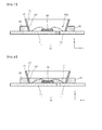
- FIG. 1 is a schematic cross-sectional view of a light emitting element package according to an embodiment of the present invention
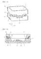
- FIG. 2 is a partial schematic perspective view of the light emitting element package of FIG. 1 .
- the cross-sectional view of FIG. 1 may be understood to be one taken along line I-I of FIG. 2 .
- the light emitting element package according to this embodiment includes a package and a reflection structure 40 as illustrated in FIGS. 1 and 2 .
- the package includes a lead frame 10, a light emitting element 20, and a molded material 30, and the reflection structure 40 includes a supporting portion 41 and a radial portion 42.
- the lead frame 10 includes a first lead 11 and a second lead 12.
- the lead frame 10 may further include another lead(s).
- the lead frame 10 may include a die pad for mounting the light emitting element 20 to be described below, and first and second leads spaced apart from the die pad.
- the light emitting element 20 is provided on the lead frame 10, for example, on the first lead 11 as illustrated in FIGS. 1 and 2 .
- the light emitting element 20 is an element for emitting light by receiving an electrical signal and may be used as a light source for various electronic devices.
- the light emitting element include a diode of a compound semiconductor, and may be referred to as a light emitting diode (LED).
- the LED may emit light of various colors depending on materials of the compound semiconductor.
- the light emitting element 20 may be electrically connected to the first lead 11 and/or the second lead 12, either by an electrically conductive adhesive member or through wiring. Referring to FIG. 1 , the light emitting element 20 is illustrated to be electrically connected to each of the first and second leads 11 and 12 through wiring. Wiring is not illustrated in FIG. 2 .
- the molded material 30 may be connected to the lead frame 10 to form an external shape of the whole light emitting element package.
- the molded material 30 has an opening 30a through which light generated by the light emitting element 20 passes.
- the molded material 30 is illustrated to have the opening 30a capable of allowing light generated by the light emitting element 20 to proceed in the positive z direction.
- the molded material 30 may be formed of a resin by, for example, transfer molding. Various modifications are possible and thus the molded material 30 may be formed by injection molding other than transfer molding.
- the resin for the molded material 30 may include, for example, epoxy.
- a first resin layer 51 may be provided within the opening 30a of the molded material 30 such that the light emitting element 20 is covered and protected against, for example, external moisture.
- a fluorescent material may be mixed into the first resin layer 51 and the opening 30a of the molded material 30 may be completely or partially filled with the first resin layer 51.
- the opening may be partially filled with the first resin layer 51 mixed with the fluorescent material, and a (transparent) filler having no fluorescent material may be additionally provided to fill the remaining area.
- the opening 30a of the molded material 30 is filled with the first resin layer 51, the opening will be filled as high as the top edge of the opening 30a of the molded material 30, that is, the bottom edge of the supporting portion 41 of the reflection structure 40, which will be described below.
- the first resin layer 51 is not illustrated in FIG. 2 .
- the reflection structure 40 has an opening that corresponds to the opening 30a of the molded material 30, and contacts the molded material 30.
- the reflection structure 40 may be formed of a metallic material having excellent thermal conductivity.
- the reflection structure 40 may include the supporting portion 41 and the radial portion 42.
- the supporting portion 41 contacts the molded material 30 and may be continuously provided along the circumference of the opening 30a of the molded material 30.
- the supporting portion 41 is illustrated to continuously surround the opening 30a of the molded material 30 in FIGS. 1 and 2 .
- the radial portion 42 is provided to contact the supporting portion 41.
- the radial portion 42 is illustrated to contact the supporting portion 41 and also contact a top surface of the molded material 30 in a light emitting direction (the positive z direction) in FIGS. 1 and 2 , but the present invention is not limited thereto. That is, the radial portion 42 may not contact the molded material 30 but contact the supporting portion 41 only.
- the radial portion 42 and the supporting portion 41 may be provided as one body.
- the radial portion 42 has a radial shape.
- the radial portion 42 may be formed in a radial shape extending radially from the molded material relative to a direction along which light generated by the light emitting element emits (the positive z direction).
- the radial shape of the radial portion 42 may be formed with respect to an axis that passes through the centers of the light emitting element 20 and the opening 30a of the molded material 30 (z axis).
- a second resin layer 52 may be further provided.
- the second resin layer 52 covers the first resin layer 51 and contacts the radial portion 42.
- the second resin layer 52 contacting the radial portion 42 may be understood to be the second resin layer 52 contacting an internal radial surface of the radial portion 42.
- the second resin layer 52 may be formed of a light-transmitting material, e.g., an epoxy or silicone resin.
- the second resin layer 52 contacts the first resin layer 51 and the radial portion 42 (radiation surface) and thus may prevent the reflection structure 40 from being separated from, for example, the molded material 30.
- the second resin layer 52 may fill the reflection structure 40 as high as the top edge of the supporting portion 41 as illustrated in FIG. 1 .
- the second resin layer 52 is not illustrated in FIG. 2 .
- the first resin layer 51 into which a fluorescent material is mixed, is provided in the opening 30a of the molded material 30 to cover the light emitting element 20, and the second resin layer 52 is provided to cover the first resin layer 51 and contact the radial portion 42 (radiation surface) in the above description
- the relative positions of the first and second resin layers 51 and 52 may be switched.
- a light-transmitting second resin layer may be provided in the opening 30a of the molded material 30 to cover the light emitting element 20, and a first resin layer, into which a fluorescent material is mixed, may be provided to cover the second resin layer and contact the radial portion 42 (radiation surface).
- the distance between the light emitting element 20 and the first resin layer into which the fluorescent material is mixed may be controlled using the second resin layer. If the distance between the light emitting element 20 and the first resin layer into which the fluorescent material is mixed decreases, the color temperature of light ultimately emitted to the outside is lowered. Consequently, the color temperature of light ultimately emitted to the outside may be controlled by adjusting the thickness of the second resin layer.
- the light emitting element 20 generates not only light but also a considerable amount of heat.
- heat generated by a light emitting element may not be easily discharged to the outside.
- a molded material may inflate or the life span of the light emitting element shortened.
- the light emitting element package according to the this embodiment includes the reflection structure 40, provided near the light emitting element 20 and contacting the molded material 30, and thus heat generated by the light emitting element 20 may be effectively discharged to the outside through the reflection structure 40.
- the radial portion 42 of the reflection structure 40 has a radial-shaped structure that is open to the outside of the molded material 30, and thus the heat generated by the light emitting element 20 and absorbed by the reflection structure 40 may be effectively discharged to the outside.
- Some of the light generated by the light emitting element 20 proceeds along a direction between the positive z direction and the positive x direction, as well as along the positive z direction.
- the luminance in a forward direction of the light emitting element package may be greatly increased by having the above described light reflected on the internal surface 42' of the radial portion 42 of the reflection structure and then proceed approximately along the positive z direction. That is, the internal surface 42' of the radial portion 42 of the reflection structure 40 may function as a reflective surface together with a tilted side surface 30' of the opening 30a of the molded material 30.
- a reflective portion may be formed only of the internal side surface 30' of the opening 30a of the molded material 30, but there may exist light that proceeds along a direction between the positive z direction and the positive x direction without reaching the internal side surface 30' of the opening 30a of the molded material 30.
- the above described light may also be reflected on the internal surface 42' of the radial portion 42 provided outside the molded material 30 and then proceed approximately along the positive z direction.
- the internal surface 42' of the radial portion 42 of the reflection structure 40 may be coated with a reflective material such as silver to improve reflectivity.
- a reflective material such as silver to improve reflectivity.
- parts other than the internal surface 42' may also be coated.
- FIGS. 3 and 4 are schematic cross-sectional views showing a manufacturing method of a light emitting element package, according to another embodiment of the present invention.
- the package that includes the lead frame 10, the light emitting element 20, and the molded material 30, and the reflection structure 40 that includes the supporting portion 41 and the radial portion 42 are prepared.
- the package includes the first resin layer 51 that fills the opening 30a of the molded material 30 to cover the light emitting element 20.
- the package and the reflection structure 40 are aligned to contact each other as illustrated in FIG. 4 , and then the second resin layer 52 is formed on the first resin layer 51, thereby manufacturing the light emitting element package illustrated in FIG. 1 .
- the second resin layer 52 may prevent the reflection structure 40 from being separated from the molded material 30.
- One package and one reflection structure 40 are aligned and combined in FIG. 3 and 4 , but the present invention is not limited thereto.
- a plurality of lead frames 10 of packages may be aligned and connected to each other, a plurality of reflection structures 40 may be aligned and connected to each other, and then the packages and the reflection structures 40 may be combined and cut, thereby simultaneously manufacturing a plurality of light emitting element packages each of which having a reflection structure.
- This also applies to the following embodiments and modifications thereof.
- the package that includes the first resin layer 51 filling the opening 30a of the molded material 30 to cover the light emitting element 20 is prepared as illustrated in FIG. 3 , the package and the reflection structure 40 are aligned to contact each other as illustrated in FIG. 4 , and then the second resin layer 52 is formed on the first resin layer 51, thereby manufacturing the light emitting element package illustrated in FIG. 1 .
- the present invention is not limited thereto.
- a package that includes a light-transmitting second resin layer filling the opening 30a of the molded material 30 to cover the light emitting element 20 may be prepared, the package and the reflection structure 40 may be aligned to contact each other, and then a first resin layer into which a fluorescent material is mixed may be formed on the second resin layer, thereby manufacturing a light emitting element package.
- the distance between the light emitting element 20 and the first resin layer into which the fluorescent material is mixed may be controlled using the second resin layer. If the distance between the light emitting element 20 and the first resin layer into which the fluorescent material is mixed decreases, the color temperature of light ultimately emitted to the outside is lowered. Consequently, the color temperature of light ultimately emitted to the outside may be controlled by adjusting the thickness of the second resin layer.
- FIGS. 5 and 6 are schematic cross-sectional views showing a manufacturing method of a light emitting element package, according to yet another embodiment of the present invention.
- the package that includes the lead frame 10, the light emitting element 20, and the molded material 30, and the reflection structure 40 that includes the supporting portion 41 and the radial portion 42 are prepared.
- the package does not include the first resin layer 51.
- the package and the reflection structure 40 are aligned to contact each other as illustrated in FIG. 6 , the first resin layer 51 that fills the opening 30a of the molded material 30 to cover the light emitting element 20 is formed, and then the second resin layer 52 is formed on the first resin layer 51, thereby manufacturing the light emitting element package illustrated in FIG. 1 .
- the second resin layer 52 may prevent the reflection structure 40 from being separated from the molded material 30.
- the first resin layer 51 into which a fluorescent material is mixed, may not only fill the opening 30a of the molded material 30 to cover the light emitting element 20 but also contact the reflection structure 40, without a second resin layer being formed.
- the first resin layer 51 may contact part of the radial portion 42, or may completely fill the opening of the radial portion 42 lest the internal surface 42' of the radial portion 42 is exposed.
- a second resin layer may fill the opening 30a of the molded material 30 to cover the light emitting element 20, and then a first resin layer into which a fluorescent material is mixed may be formed on the second resin layer.
- the second resin layer may not contact the reflection structure 40 and the first resin layer may contact the reflection structure 40, or the second resin layer may contact the reflection structure 40 and the first resin layer thereon may also contact the reflection structure 40.
- the reflection structure has been illustrated to include a supporting portion and a radial portion, but the present invention is not limited thereto. That is, the supporting portion may be part of a molded material and the reflection structure may include the radial portion only. For example, the supporting portion continuously or discretely disposed along the circumference of an opening of the molded material may be one of the components of the molded material. Furthermore, the reflection structure may include the radial portion contacting the supporting portion of the molded material and formed in a radial shape extending radially from the molded material relative to a direction along which light generated by the light emitting element emits.
- FIGS. 7 and 8 are schematic cross-sectional views showing a manufacturing method of a light emitting element package, according to yet another embodiment of the present invention.
- a structure wherein the package and the reflection structure 40 are combined is firstly prepared as illustrated in FIG. 7 .
- the reflection structure 40 has a shape different from that of the reflection structure according to the preceding embodiments.
- part of the reflection structure 40 may be inserted into the opening 30a of the molded material 30, and the other part of the reflection structure 40, protruding from the opening 30a of the molded material 30, may be formed in a radial shape extending radially from the molded material relative to a direction along which light generated by the light emitting element 20 emits. That is, unlike the preceding embodiments, the supporting portion 41 may not be provided.
- the part of the reflection structure 40 which is inserted into the opening 30a of the molded material 30, may contact an internal surface 30' of the opening 30a of the molded material 30, and may extend to a bottom surface of the opening 30a of the molded material 30 to contact the bottom surface (the first lead 11 or the second lead 12) as illustrated in FIGS. 7 and 8 .
- the reflection structure 40 may not extend to the bottom surface of the opening 30a of the molded material 30 and may cover only part of the internal surface 30' of the opening 30a. Including the above, various modifications of this embodiment are possible.
- the first resin layer 51 is formed to cover the light emitting element 20 as illustrated in FIG. 8 .
- a fluorescent material may be mixed into the first resin layer 51.
- the first resin layer 51 may be cured and prevent the reflection structure 40 from being separated from the molded material 30.
- a light-transmitting second resin layer may be provided on the first resin layer 51, if necessary.
- the first resin layer 51 into which the fluorescent material is mixed may not only fill the opening of the molded material 30 to cover the light emitting element 20 but also be formed such that a top surface of the first resin layer 51 is higher than that of the molded material 30, without a second resin layer being formed.
- a second resin layer may fill the opening 30a of the molded material 30 to cover the light emitting element 20, and then a first resin layer into which a fluorescent material is mixed may be formed on the second resin layer.
- the light emitting element package illustrated in FIG. 8 may be understood to be a light emitting element package according to yet another embodiment of the present invention.
- the reflection structure 40 since the reflection structure 40 contacts the first and second leads 11 and 12, the first and second leads 11 and 12 need to be insulated from each other. Accordingly, the reflection structure 40 may have a radial shape and be divided into at least two parts spaced apart from each other. A first part of the reflection structure 40, which contacts the first lead 11, and a second part of the reflection structure 40, which contacts the second lead 12, may be spaced apart from each other, and have an insulating material filled therebetween.
- FIG. 9 is a partial schematic perspective view of a light emitting element package according to yet another embodiment of the present invention.
- the reflection structure 40 includes the supporting portion 41 and a radial portion (not shown).
- the supporting portion 41 contacts the molded material 30 but is provided not continuously but discretely along the circumference of the opening 30a of the molded material 30. That is, the supporting portion 41 has discontinuous parts 41 a. Two discontinuous parts 41 a are illustrated in FIG. 9 , but the number of the discontinuous parts 41 a may vary and the width of the discontinuous parts 41 a may be greater than that illustrated in FIG. 9 .
- the supporting portion 41 serves to support the radial portion (not shown), even when the supporting portion 41 has the discontinuous parts 41a, manufacturing costs may be reduced, without deteriorating heat radiation function and forward direction luminance.
- a supporting portion may not be part of the reflection structure 40. That is, the supporting portion may be part of the molded material 30, and the reflection structure 40 may have the radial portion only. Even here, the supporting portion, which is part of the molded material 30, may be provided not continuously but discretely along the circumference of the opening 30a of the molded material 30.
- FIG. 10 is a schematic perspective view of a light emitting element package according to yet another embodiment of the present invention
- FIG. 11 is an exploded perspective view of the light emitting element package of FIG. 10
- FIG. 12 is a schematic cross-sectional view taken along line XII-XII of FIG. 10 .
- the light emitting element package according to this embodiment may include a lead frame, a light emitting element 20, a molded material 30, and a reflection structure 40, as illustrated in FIGS. 10 to 12 .
- the molded material 30 may include a supporting portion 33 provided continuously or discretely along the circumference of the opening 30a.
- the supporting portion 33 may be provided adjacent to the exterior part of the opening 30a along the circumference of the opening 30a.
- the supporting portion 33 is illustrated to discretely surround the opening 30a of the molded material 30 in FIGS. 10 to 12 .
- the supporting portion 33 is not limited thereto and may continuously surround the opening 30a of the molded material 30 as described in the preceding embodiments. If the supporting portion 33 discretely surrounds the opening 30a of the molded material 30 as illustrated in FIGS. 10 to 12 , this may be understood to be that recesses or concave and convex portions are formed in the molded material 30.
- the opening 30a may be formed in the center of a top surface of the molded material 30, and the light emitting element 20 may be mounted at the central part of the opening 30a.
- the supporting portion 33 may extend along the circumference of the opening 30a of the molded material 30 and protrude from corners of the molded material 30 along the positive z direction.
- a surface of the supporting portion 33,facing the opening 30a of the molded material 30 may be formed in a radial shape extending radially relative to a direction along which light generated by the light emitting element 20 emits (e.g., the positive z direction).
- the supporting portion 33 may have an internal surface that has a downward inclination with respect to the opening 30a of the molded material 30. This allows the supporting portion 33 to more stably support the reflection structure 40 that will be described below. This also allows the supporting portion 33 to more accurately guide or define a location wherein the reflection structure 40 is combined.
- a resin layer 60 may be provided on the light emitting element 20 in the opening 30a of the molded material 30 to cover the light emitting element 20 so as to protect the light emitting element 20 from, for example, external moisture.
- a fluorescent material may be mixed into the resin layer 60 and the opening 30a of the molded material 30 may be completely or partially filled with the resin layer 60.
- the opening may be partially filled with the resin layer 60 into which the fluorescent material is mixed, and a (transparent) filler having no fluorescent material may be additionally provided to fill the remaining area.
- the resin layer 60 or the filler may be fill not only the opening 30a of the molded material 30 but also fill the reflection structure 40 to a bottom end or a top end, which will be described below.
- the reflection structure 40 has an opening that corresponds to the opening 30a of the molded material 30 and may contact the molded material 30. As described above, if the supporting portion 33 discretely surrounds the opening 30a of the molded material 30, that is, if it is understood that recesses or concave and convex portions are formed in the molded material 30, the reflection structure 40 may be fitted into the recesses or concave and convex portions.
- the reflection structure 40 may include a metal having excellent thermal conductivity.
- the reflection structure 40 may also include a radial surface 45 formed in a radial shape extending radially from the molded material relative to a direction along which light generated by the light emitting element 20 emits.
- the reflection structure 40 may be configured to reflect light emitted by the light emitting element 20 such that the light proceeds approximately along the positive z direction. Particularly, since some of the light generated by the light emitting element 20 proceeds between the positive z direction and the positive y direction, as well as along the positive z direction The luminance in a forward direction of the light emitting element package may be greatly increased and a beam angle of the light emitted by the light emitting element package may be narrowed by having the above described light reflected on the radial surface 45 of the reflection structure 40 and then proceed approximately along the positive z direction. That is, the radial surface 45 of the reflection structure 40 together with a inclined internal side surface of the opening 30a of the molded material 30 may function as a reflective surface.
- a reflective portion may be formed only of the internal side surface of the opening 30a of the molded material 30, but there may exist light that proceeds along a direction between the positive z direction and the positive y direction without reaching the internal side surface of the opening 30a of the molded material 30.
- the above described light may also be reflected on the radial surface 45 provided outside the molded material 30 and then proceed approximately along the positive z direction.
- the cross-section of the radial surface 45 of the reflection structure 40 may be flat or bent.
- the cross-section of the radial surface 45 of the reflection structure 40 may be flat. That is, the radial surface 45 of the reflection structure 40 may form a predetermined angle a with a main emission direction along which light generated by the light emitting element 20 emits.
- the main emission direction refers to the positive z direction.
- the predetermined angle a may be equal to or greater than 10° and equal to or less than 20°.
- FIG. 13 is a schematic cross-sectional view of a light emitting element package according to yet another embodiment of the present invention.
- FIG. 13 is a cross-sectional view of the light emitting element package according to the present invention, taken along a line located similar to the line XII-XII of FIG. 10 .
- the radial surface 45 of the reflection structure 40 may form a first angle a1 with the positive z direction from a point where the radial surface contacts the molded material 30 to a first point 43 away from the molded material 30, and form a second angle a2 from the first point 43 to a second point 44 further away from the molded material 30 compared to the first point 43.
- the second angle a2 may be greater than the first angle a1.
- the first angle a1 may be about 10° and the second angle a2 may be about 20°.
- the second point 44 may be, for example, an end portion of the reflection structure 40. That is, the first point 43 may be a certain point between two end portions of an internal surface of the reflection structure 40, located along the positive z direction, i.e., between an end portion along a direction toward the molded material 30 (the negative z direction) and an end portion along an emission direction of light (the positive z direction).
- each of the first and second points 43 and 44 may be continuously provided along the circumference of the opening 30a of the molded material 30 to form an encircling line.
- the radial surface 45 is inclined by the predetermined angle a as described above, light emitted from the light emitting element 20 may be radiated onto the radial surface 45. Accordingly, a beam angle of light emitted from the light emitting element package may be narrowed.
- the radial surface 45 of the reflection structure 40 may be coated with a reflective material such as silver to improve reflectivity. For convenience, portions other than the radial surface 45 may also be coated.
- the reflection structure 40 may have a shape that corresponds to the supporting portion 33, thereby contacting the molded material 30.
- the reflection structure 40 may also have a continuous shape that corresponds to the shape of the supporting portion 33.
- the reflection structure 40 may also have a discrete shape to be inserted between the supporting portions 33.
- FIG. 14 is a schematic cross-sectional view showing paths of light emitted from the light emitting element package according to embodiments of the present invention. Although FIG. 14 schematically illustrates paths of light emitted from the light emitting element package illustrated in FIG. 12 , the paths of light may be equally or similarly applied to the light emitting element package illustrated in FIG. 13 .
- light emitted from the light emitting element 20 may directly reach area A of a illuminated surface 70 along a first path 21, reach area B of the illuminated surface 70 after being reflected on the molded material 30 along a second path 22, and reach area C of the illuminated surface 70 after being reflected on the reflection structure 40 along a third path 23.
- the luminance of area A may be the highest, the luminance of area B may be the second highest, and the luminance of area C may be the lowest. That is, the luminance is lowered away from an optical axis. In particular, the luminance may be greatly lowered from area B to area C.
- the reflection structure 40 may have a higher reflectivity than that of the molded material 30.
- the reflection structure 40 may include a metal and thus have a higher reflectivity than that of the molded material 30 that is formed of a resin material. Accordingly, the luminance of light projected onto area C along the third path 23 may increase compared to a conventional way due to the high reflectivity of the reflection structure 40. Therefore, the luminance may not be rapidly reduced but gradually reduced from area A to area C and, particularly, the change in the luminance may be gradual or almost no change may occur from area B to area C. As such, light having an almost uniform luminance may be effectively projected onto the whole illuminated surface 70.
- FIG. 15 is a schematic graph showing a beam angle of light emitted from the light emitting element package according to embodiments of the present invention.
- a conventional light emitting element package has a peak of optical power in an optical axis direction, and emits light in such a manner that the optical power is not rapidly but gradually reduced as an angle with the optical axis is increased. Furthermore, due to a large beam angle, the conventional light emitting element package has a small amount of reduction in optical power even considerably far away from an optical axis, and thus is used for lighting by having an overall luminance of light emitted from a light emitting element package be gradually reduced over a wide range.
- light emitted from the light emitting element 20 may be reflected by the reflection structure 40 and thus the optical power near an optical axis may be almost uniform even away from the optical axis. Furthermore, the luminance of an illuminated area may be increased by narrowing a beam angle. Thus, light emitted from the light emitting element package may have a uniform and high luminance near the optical axis even away from the optical axis. As such, when the light emitting element package is used as a flash for a mobile phone, a camera, etc., light having a high and uniform luminance may be effectively projected onto a whole area to be photographed. That is, the above-described optical lenses are for a flash and may be combined with the light emitting element package to effectively project light having a uniform intensity onto an illuminated area.
- FIG. 16 is a partial schematic perspective view of a light emitting element according to yet another embodiment of the present invention.
- an adhesive layer 60 will be described with reference to FIGS. 12 , 13 , and 16 .
- the adhesive layer 60 may be provided at least part of a region between the molded material 30 and the reflection structure 40 to fix the reflection structure 40 onto the molded material 30.
- the adhesive layer 60 may be provided between the supporting portion 33 of the molded material 30 and the reflection structure 40 as illustrated in FIG. 12 . That is, it would be preferable that an exposed portion of the adhesive layer 60 is minimized and, due to a low reflectivity of light, the adhesive layer 60 may not be exposed between the radiation surface 45 of the reflection structure 40 and the opening 30a of the molded material 30. Accordingly, as illustrated in FIGS. 12 and 13 , the adhesive layer 60 may be provided between the supporting portion 33 and the reflection structure 40, and may not be provided between the reflection structure 40 and part of the molded material 30 that is adjacent to the opening 30a.
- the thickness of the adhesive layer 60 may vary according to locations, to maximize adhesive force while minimizing the amount of the adhesive layer. Particularly, a first thickness 51 in an area adjacent to the light emitting element 20 may be greater than a second thickness 52 in an area away from the light emitting element 20. Here, the thickness of the adhesive layer 60 may be gradually reduced away from the light emitting element 20.
- the adhesive layer 60 may have a sufficiently large thickness in areas adjacent to the light emitting element 20, thereby ensuring a strong adhesion between the molded material 30 and the reflection structure 40, and have a reduced thickness in areas away from the light emitting element 20, thereby reducing the amount of material used to manufacture the light emitting element package and manufacturing costs.
- a light emitting element package may include a lead frame, a light emitting element 20, a molded material 30, a reflection structure 40, and an adhesive layer 60.
- the light emitting element package according to this embodiment is the same as or similar to the light emitting element package according to the preceding embodiments. Thus, repeated description thereof will be omitted.
- the molded material 30 may be combined with the lead frame and have the opening 30a for emitting light generated by the light emitting element 20. That is, unlike the molded material 30 according to the preceding embodiments, the molded material 30 according to this embodiment may not include the supporting portion 33.
- the reflection structure 40 may have an opening that corresponds to the opening 30a of the molded material 30, and contact the molded material 30.
- the reflection structure 40 according to this embodiment is the same as or similar to the reflection structure 40 according to the preceding embodiments, but may optionally have a shape that corresponds to the supporting portion 33.
- the adhesive layer 60 may be provided at least partly between the molded material 30 and the reflection structure 40 to fix the reflection structure 40 onto the molded material 30.
- the first thickness 51 of the adhesive layer 60 in areas adjacent to the light emitting element 20 may be greater than the second thickness 52 of the adhesive layer 60 in areas away from the light emitting element 20.
- the adhesive layer 60 according to this embodiment is the same as or similar to the adhesive layer 60 according to the preceding embodiments, and thus a detailed description thereof will be omitted.
- the adhesive layer 60 is used to maintain adhesive force.
- FIG. 17 is a schematic side elevation view of a backlight unit according to an embodiment of the present invention.
- the backlight unit includes a frame 110, a reflective sheet 115 on part of the frame 110, a light guide plate 120 on the reflective sheet 115, and a light emitting element package 100 on other part of the frame 110 and configured to illuminate the light guide plate 120.
- the light emitting element package 100 may be any one of the light emitting element packages according to the preceding embodiments and modifications thereof.
- the light emitting element package 100 may be connected to a printed circuit board 112.
- the whole backlight unit may have improved heat radiation function and improved luminance of emitted light.
- the present invention is not limited thereto and but applicable to a direct-type backlight unit in which a light guide plate is provided on or above a reflective sheet and a light emitting element package is provided under or below the light guide plate.
- the present invention may be used to manufacture a light emitting element package having excellent heat radiation performance and high luminance, and a backlight unit including the same.
Landscapes
- Led Device Packages (AREA)
- Planar Illumination Modules (AREA)
- Physics & Mathematics (AREA)
- Engineering & Computer Science (AREA)
- Microelectronics & Electronic Packaging (AREA)
- General Physics & Mathematics (AREA)
- Optics & Photonics (AREA)
Abstract
Description
- The present invention relates to a light emitting element package and a backlight unit including the same. More particularly, the present invention relates to a light emitting element package having excellent heat radiation performance and high luminance, and a backlight unit including the same.
- In general, a light emitting element is used as a light source of a backlight unit in an electronic device, e.g., display device. A light emitting element may be packaged in various ways before being connected to a backlight module and a backlight unit includes a packaged light emitting element.
- The light emitting element of the light emitting element package generates not only light but also a considerable amount of heat.
- However, in the above-described conventional light emitting element package, heat generated by the light emitting element may not be easily discharged to the outside. As a result, a molded material may inflate or the life span of the light emitting element may be shortened.
- The present invention has been made in an effort to solve various problems including the above problem, and provides a light emitting element package having excellent heat radiation performance and high luminance, and a backlight unit including the same. However, the scope of the present invention is not limited thereto.
- According to an aspect of the present invention, there is provided a light emitting element package including a lead frame, a light emitting element on the lead frame, a molded material combined with the lead frame and having an opening for emitting light generated by the light emitting element, and a reflection structure having an opening that corresponds to the opening of the molded material, and contacting the molded material.
- The reflection structure may include a supporting portion contacting the molded material and provided continuously or discretely along a circumference of the opening of the molded material, and a radial portion contacting the supporting portion and extending radially from the molded material relative to a direction along which light generated by the light emitting element emits.
- The molded material may include a supporting portion provided continuously or discretely along a circumference of the opening of the molded material, and the reflection structure may include a radial portion contacting the supporting portion and having a radial shape extending radially from the molded material relative to a direction along which light generated by the light emitting element emits.
- The molded material may include a supporting portion provided continuously or discretely along a circumference of the opening of the molded material, and the reflection structure may have a shape that corresponds to the supporting portion of the molded material and contact the molded material.
- Recesses or concave and convex portions may be provided on the molded material, and the reflection structure may be fitted into the recesses or concave and convex portions.
- The light emitting element package may further include an adhesive layer provided in at least part of a region between the molded material and the reflection structure to fix the reflection structure onto the molded material.
- The adhesive layer may have a first thickness in an area adjacent to the light emitting element and a second thickness in an area away from the light emitting element, and the first thickness may be greater than the second thickness.
- The thickness of the adhesive layer may be gradually reduced away from the light emitting element.
- The reflection structure may include a radial surface formed in a radial shape extending radially from the molded material relative to a direction along which light generated by the light emitting element emits.
- The radial surface of the reflection structure may form a predetermined angle with a main emission direction of light generated by the light emitting element emits.
- The predetermined angle may be equal to or greater than 10° and equal to or less than 20°.
- The radial surface of the reflection structure may form a first angle with to a main emission direction of light generated by the light emitting element, from a point where the radial surface contacts the molded material to a first point away from the molded material, and form a second angle with the main emission direction from the first point to a second point further away from the molded material compared to the first point, and the second angle may be greater than the first angle.
- The light emitting element package may further include a first resin layer that includes a fluorescent material and be provided in the opening of the molded material to cover the light emitting element.
- The light emitting element package may further include a light-transmitting second resin layer that covers the first resin layer and contacts the radial surface.
- The light emitting element package may further include a light-transmitting second resin layer provided in the opening of the molded material to cover the light emitting element, and a first resin layer that includes a fluorescent material, covers the second resin layer, and contacts the radial surface.
- The reflection structure may comprise metal.
- A surface of the supporting portion facing the opening of the molded material may have a radial shape extending radially relative to a direction along which light generated by the light emitting element emits.
- Part of the reflection structure may be inserted into the opening of the molded material, and the other part of the reflection structure, protruding from the opening of the molded material may have a radial shape extending radially from the molded material relative to a direction along which light generated by the light emitting element emits.
- According to another aspect of the present invention, there is provided a light emitting element package including a lead frame, a light emitting element on the lead frame, a molded material combined with the lead frame and having an opening for emitting light generated by the light emitting element, a reflection structure having an opening that corresponds to the opening of the molded material, and contacting the molded material, a supporting portion provided discretely or continuously on the molded material to fix the reflection structure onto the molded material, and an adhesive layer provided in at least part of a region between the molded material and the reflection structure, and having a first thickness in an area adjacent to the light emitting element and a second thickness in an area away from the light emitting element, wherein the first thickness is greater than the second thickness.
- According to yet another aspect of the present invention, there is provided a backlight unit including a reflective sheet, a light guide plate on or above the reflective sheet, and a light emitting element package configured to illuminate the light guide plate.
- According to an embodiment of the present invention, a light emitting element package having excellent heat radiation performance and high luminance, and a backlight unit including the same may beprovided. However, the scope of the present invention is not limited thereto.
-
-
FIG. 1 is a schematic cross-sectional view of a light emitting element package according to an embodiment of the present invention; -
FIG. 2 is a partial schematic perspective view of the light emitting element package ofFIG. 1 ; -
FIGS. 3 and 4 are schematic cross-sectional views showing a manufacturing method of a light emitting element package, according to another embodiment of the present invention; -
FIGS. 5 and 6 are schematic cross-sectional views showing a manufacturing method of a light emitting element package, according to yet another embodiment of the present invention; -
FIGS. 7 and 8 are schematic cross-sectional views showing a manufacturing method of a light emitting element package, according to yet another embodiment of the present invention; -
FIG. 9 is a partial schematic perspective view of a light emitting element package according to yet another embodiment of the present invention; -
FIG. 10 is a schematic perspective view of a light emitting element package according to yet another embodiment of the present invention; -
FIG. 11 is an exploded perspective view of the light emitting element package ofFIG. 10 ; -
FIG. 12 is a schematic cross-sectional view taken along line XII-XII ofFIG. 10 ; -
FIG. 13 is a schematic cross-sectional view of a light emitting element package according to yet another embodiment of the present invention; -
FIG. 14 is a schematic cross-sectional view showing paths of as well as surfaces illuminated by light emitted from the light emitting element package according to embodiments of the present invention; -
FIG. 15 is a schematic graph showing a beam angle of light emitted from the light emitting element package according to embodiments of the present invention; -
FIG. 16 is a partial schematic perspective view of a light emitting element according to yet another embodiment of the present invention; and -
FIG. 17 is a schematic side elevation view of a backlight unit according to an embodiment of the present invention. - Hereinafter, embodiments of the present invention will be described in detail with reference to the attached drawings. The present invention may, however, be embodied in many different forms and should not be construed as being limited to the embodiments set forth herein; rather, these embodiments are provided so that this disclosure will be thorough and complete, and will fully convey the concept of the invention to a person having ordinary skill in the art. In the drawings, the sizes of elements may be exaggerated or reduced for convenience of explanation.
- In the following description, x, y, and z axes are not limited to three axes on a Cartesian coordinate system, and may be construed in a broad sense to include those axes. For example, the x, y, and z axes may be perpendicular to each other but may also refer to different non-perpendicular directions.
-
FIG. 1 is a schematic cross-sectional view of a light emitting element package according to an embodiment of the present invention, andFIG. 2 is a partial schematic perspective view of the light emitting element package ofFIG. 1 . The cross-sectional view ofFIG. 1 may be understood to be one taken along line I-I ofFIG. 2 . The light emitting element package according to this embodiment includes a package and areflection structure 40 as illustrated inFIGS. 1 and 2 . The package includes alead frame 10, alight emitting element 20, and a moldedmaterial 30, and thereflection structure 40 includes a supportingportion 41 and aradial portion 42. - The
lead frame 10 includes afirst lead 11 and asecond lead 12. Thelead frame 10 may further include another lead(s). For example, thelead frame 10 may include a die pad for mounting thelight emitting element 20 to be described below, and first and second leads spaced apart from the die pad. - The
light emitting element 20 is provided on thelead frame 10, for example, on thefirst lead 11 as illustrated inFIGS. 1 and 2 . Thelight emitting element 20 is an element for emitting light by receiving an electrical signal and may be used as a light source for various electronic devices. For example, the light emitting element include a diode of a compound semiconductor, and may be referred to as a light emitting diode (LED). The LED may emit light of various colors depending on materials of the compound semiconductor. - The
light emitting element 20 may be electrically connected to thefirst lead 11 and/or thesecond lead 12, either by an electrically conductive adhesive member or through wiring. Referring toFIG. 1 , thelight emitting element 20 is illustrated to be electrically connected to each of the first and second leads 11 and 12 through wiring. Wiring is not illustrated inFIG. 2 . - The molded
material 30 may be connected to thelead frame 10 to form an external shape of the whole light emitting element package. The moldedmaterial 30 has anopening 30a through which light generated by thelight emitting element 20 passes. InFIGS. 1 and 2 , the moldedmaterial 30 is illustrated to have theopening 30a capable of allowing light generated by thelight emitting element 20 to proceed in the positive z direction. - The molded
material 30 may be formed of a resin by, for example, transfer molding. Various modifications are possible and thus the moldedmaterial 30 may be formed by injection molding other than transfer molding. The resin for the moldedmaterial 30 may include, for example, epoxy. - A
first resin layer 51 may be provided within theopening 30a of the moldedmaterial 30 such that thelight emitting element 20 is covered and protected against, for example, external moisture. A fluorescent material may be mixed into thefirst resin layer 51 and theopening 30a of the moldedmaterial 30 may be completely or partially filled with thefirst resin layer 51. The opening may be partially filled with thefirst resin layer 51 mixed with the fluorescent material, and a (transparent) filler having no fluorescent material may be additionally provided to fill the remaining area. When theopening 30a of the moldedmaterial 30 is filled with thefirst resin layer 51, the opening will be filled as high as the top edge of theopening 30a of the moldedmaterial 30, that is, the bottom edge of the supportingportion 41 of thereflection structure 40, which will be described below. Thefirst resin layer 51 is not illustrated inFIG. 2 . - The
reflection structure 40 has an opening that corresponds to theopening 30a of the moldedmaterial 30, and contacts the moldedmaterial 30. Thereflection structure 40 may be formed of a metallic material having excellent thermal conductivity. Particularly, thereflection structure 40 may include the supportingportion 41 and theradial portion 42. - The supporting
portion 41 contacts the moldedmaterial 30 and may be continuously provided along the circumference of theopening 30a of the moldedmaterial 30. The supportingportion 41 is illustrated to continuously surround theopening 30a of the moldedmaterial 30 inFIGS. 1 and 2 . - The
radial portion 42 is provided to contact the supportingportion 41. Theradial portion 42 is illustrated to contact the supportingportion 41 and also contact a top surface of the moldedmaterial 30 in a light emitting direction (the positive z direction) inFIGS. 1 and 2 , but the present invention is not limited thereto. That is, theradial portion 42 may not contact the moldedmaterial 30 but contact the supportingportion 41 only. Theradial portion 42 and the supportingportion 41 may be provided as one body. - The
radial portion 42 has a radial shape. Particularly, theradial portion 42 may be formed in a radial shape extending radially from the molded material relative to a direction along which light generated by the light emitting element emits (the positive z direction). The radial shape of theradial portion 42 may be formed with respect to an axis that passes through the centers of thelight emitting element 20 and theopening 30a of the molded material 30 (z axis). - A
second resin layer 52 may be further provided. Here, thesecond resin layer 52 covers thefirst resin layer 51 and contacts theradial portion 42. Thesecond resin layer 52 contacting theradial portion 42 may be understood to be thesecond resin layer 52 contacting an internal radial surface of theradial portion 42. - The
second resin layer 52 may be formed of a light-transmitting material, e.g., an epoxy or silicone resin. Thesecond resin layer 52 contacts thefirst resin layer 51 and the radial portion 42 (radiation surface) and thus may prevent thereflection structure 40 from being separated from, for example, the moldedmaterial 30. Thesecond resin layer 52 may fill thereflection structure 40 as high as the top edge of the supportingportion 41 as illustrated inFIG. 1 . Thesecond resin layer 52 is not illustrated inFIG. 2 . - Although the
first resin layer 51, into which a fluorescent material is mixed, is provided in theopening 30a of the moldedmaterial 30 to cover thelight emitting element 20, and thesecond resin layer 52 is provided to cover thefirst resin layer 51 and contact the radial portion 42 (radiation surface) in the above description, the relative positions of the first and second resin layers 51 and 52 may be switched. For example, a light-transmitting second resin layer may be provided in theopening 30a of the moldedmaterial 30 to cover thelight emitting element 20, and a first resin layer, into which a fluorescent material is mixed, may be provided to cover the second resin layer and contact the radial portion 42 (radiation surface). - Here, since the second resin layer is provided between the light emitting
element 20 and the first resin layer into which the fluorescent material is mixed, the distance between the light emittingelement 20 and the first resin layer into which the fluorescent material is mixed may be controlled using the second resin layer. If the distance between the light emittingelement 20 and the first resin layer into which the fluorescent material is mixed decreases, the color temperature of light ultimately emitted to the outside is lowered. Consequently, the color temperature of light ultimately emitted to the outside may be controlled by adjusting the thickness of the second resin layer. - As described above, the
light emitting element 20 generates not only light but also a considerable amount of heat. In a conventional light emitting element package, heat generated by a light emitting element may not be easily discharged to the outside. As a result, a molded material may inflate or the life span of the light emitting element shortened. - The light emitting element package according to the this embodiment includes the
reflection structure 40, provided near thelight emitting element 20 and contacting the moldedmaterial 30, and thus heat generated by thelight emitting element 20 may be effectively discharged to the outside through thereflection structure 40. In particular, theradial portion 42 of thereflection structure 40 has a radial-shaped structure that is open to the outside of the moldedmaterial 30, and thus the heat generated by thelight emitting element 20 and absorbed by thereflection structure 40 may be effectively discharged to the outside. - Some of the light generated by the
light emitting element 20 proceeds along a direction between the positive z direction and the positive x direction, as well as along the positive z direction. The luminance in a forward direction of the light emitting element package may be greatly increased by having the above described light reflected on the internal surface 42' of theradial portion 42 of the reflection structure and then proceed approximately along the positive z direction. That is, the internal surface 42' of theradial portion 42 of thereflection structure 40 may function as a reflective surface together with a tilted side surface 30' of theopening 30a of the moldedmaterial 30. - A reflective portion may be formed only of the internal side surface 30' of the
opening 30a of the moldedmaterial 30, but there may exist light that proceeds along a direction between the positive z direction and the positive x direction without reaching the internal side surface 30' of theopening 30a of the moldedmaterial 30. In the light emitting element package according to the current embodiment, the above described light may also be reflected on the internal surface 42' of theradial portion 42 provided outside the moldedmaterial 30 and then proceed approximately along the positive z direction. - The internal surface 42' of the
radial portion 42 of thereflection structure 40 may be coated with a reflective material such as silver to improve reflectivity. For convenience, parts other than the internal surface 42' may also be coated. -
FIGS. 3 and 4 are schematic cross-sectional views showing a manufacturing method of a light emitting element package, according to another embodiment of the present invention. Referring toFIG. 3 , the package that includes thelead frame 10, thelight emitting element 20, and the moldedmaterial 30, and thereflection structure 40 that includes the supportingportion 41 and theradial portion 42 are prepared. The package includes thefirst resin layer 51 that fills theopening 30a of the moldedmaterial 30 to cover thelight emitting element 20. - After that, the package and the
reflection structure 40 are aligned to contact each other as illustrated inFIG. 4 , and then thesecond resin layer 52 is formed on thefirst resin layer 51, thereby manufacturing the light emitting element package illustrated inFIG. 1 . Thesecond resin layer 52 may prevent thereflection structure 40 from being separated from the moldedmaterial 30. - One package and one
reflection structure 40 are aligned and combined inFIG. 3 and 4 , but the present invention is not limited thereto. For example, a plurality of lead frames 10 of packages may be aligned and connected to each other, a plurality ofreflection structures 40 may be aligned and connected to each other, and then the packages and thereflection structures 40 may be combined and cut, thereby simultaneously manufacturing a plurality of light emitting element packages each of which having a reflection structure. This also applies to the following embodiments and modifications thereof. - Meanwhile, as described above, the package that includes the
first resin layer 51 filling theopening 30a of the moldedmaterial 30 to cover thelight emitting element 20 is prepared as illustrated inFIG. 3 , the package and thereflection structure 40 are aligned to contact each other as illustrated inFIG. 4 , and then thesecond resin layer 52 is formed on thefirst resin layer 51, thereby manufacturing the light emitting element package illustrated inFIG. 1 . However, the present invention is not limited thereto. For example, a package that includes a light-transmitting second resin layer filling theopening 30a of the moldedmaterial 30 to cover thelight emitting element 20 may be prepared, the package and thereflection structure 40 may be aligned to contact each other, and then a first resin layer into which a fluorescent material is mixed may be formed on the second resin layer, thereby manufacturing a light emitting element package. - Here, since the second resin layer is provided between the light emitting
element 20 and the first resin layer into which the fluorescent material is mixed, the distance between the light emittingelement 20 and the first resin layer into which the fluorescent material is mixed may be controlled using the second resin layer. If the distance between the light emittingelement 20 and the first resin layer into which the fluorescent material is mixed decreases, the color temperature of light ultimately emitted to the outside is lowered. Consequently, the color temperature of light ultimately emitted to the outside may be controlled by adjusting the thickness of the second resin layer. -
FIGS. 5 and 6 are schematic cross-sectional views showing a manufacturing method of a light emitting element package, according to yet another embodiment of the present invention. Referring toFIG. 5 , the package that includes thelead frame 10, thelight emitting element 20, and the moldedmaterial 30, and thereflection structure 40 that includes the supportingportion 41 and theradial portion 42 are prepared. The package does not include thefirst resin layer 51. - After that, the package and the
reflection structure 40 are aligned to contact each other as illustrated inFIG. 6 , thefirst resin layer 51 that fills theopening 30a of the moldedmaterial 30 to cover thelight emitting element 20 is formed, and then thesecond resin layer 52 is formed on thefirst resin layer 51, thereby manufacturing the light emitting element package illustrated inFIG. 1 . Thesecond resin layer 52 may prevent thereflection structure 40 from being separated from the moldedmaterial 30. - However, unlike this, after the package and the
reflection structure 40 are aligned to contact each other as illustrated inFIG. 6 , thefirst resin layer 51, into which a fluorescent material is mixed, may not only fill theopening 30a of the moldedmaterial 30 to cover thelight emitting element 20 but also contact thereflection structure 40, without a second resin layer being formed. Here, thefirst resin layer 51 may contact part of theradial portion 42, or may completely fill the opening of theradial portion 42 lest the internal surface 42' of theradial portion 42 is exposed. - Alternatively, after the package and the
reflection structure 40 are aligned to contact each other as illustrated inFIG. 6 , a second resin layer may fill theopening 30a of the moldedmaterial 30 to cover thelight emitting element 20, and then a first resin layer into which a fluorescent material is mixed may be formed on the second resin layer. Here, the second resin layer may not contact thereflection structure 40 and the first resin layer may contact thereflection structure 40, or the second resin layer may contact thereflection structure 40 and the first resin layer thereon may also contact thereflection structure 40. - Heretofore, the reflection structure has been illustrated to include a supporting portion and a radial portion, but the present invention is not limited thereto. That is, the supporting portion may be part of a molded material and the reflection structure may include the radial portion only. For example, the supporting portion continuously or discretely disposed along the circumference of an opening of the molded material may be one of the components of the molded material. Furthermore, the reflection structure may include the radial portion contacting the supporting portion of the molded material and formed in a radial shape extending radially from the molded material relative to a direction along which light generated by the light emitting element emits.
-
FIGS. 7 and 8 are schematic cross-sectional views showing a manufacturing method of a light emitting element package, according to yet another embodiment of the present invention. In this embodiment, a structure wherein the package and thereflection structure 40 are combined is firstly prepared as illustrated inFIG. 7 . - Here, the
reflection structure 40 has a shape different from that of the reflection structure according to the preceding embodiments. In the manufacturing process according to this embodiment, part of thereflection structure 40 may be inserted into theopening 30a of the moldedmaterial 30, and the other part of thereflection structure 40, protruding from theopening 30a of the moldedmaterial 30, may be formed in a radial shape extending radially from the molded material relative to a direction along which light generated by thelight emitting element 20 emits. That is, unlike the preceding embodiments, the supportingportion 41 may not be provided. - Particularly, the part of the
reflection structure 40, which is inserted into theopening 30a of the moldedmaterial 30, may contact an internal surface 30' of theopening 30a of the moldedmaterial 30, and may extend to a bottom surface of theopening 30a of the moldedmaterial 30 to contact the bottom surface (thefirst lead 11 or the second lead 12) as illustrated inFIGS. 7 and 8 . Alternatively, thereflection structure 40 may not extend to the bottom surface of theopening 30a of the moldedmaterial 30 and may cover only part of the internal surface 30' of theopening 30a. Including the above, various modifications of this embodiment are possible. - After the structure wherein the package and the
reflection structure 40 are combined is prepared as described above, thefirst resin layer 51 is formed to cover thelight emitting element 20 as illustrated inFIG. 8 . A fluorescent material may be mixed into thefirst resin layer 51. Thefirst resin layer 51 may be cured and prevent thereflection structure 40 from being separated from the moldedmaterial 30. A light-transmitting second resin layer may be provided on thefirst resin layer 51, if necessary. - Unlike the above, after the structure wherein the package and the
reflection structure 40 are combined is prepared as illustrated inFIG. 7 , thefirst resin layer 51 into which the fluorescent material is mixed may not only fill the opening of the moldedmaterial 30 to cover thelight emitting element 20 but also be formed such that a top surface of thefirst resin layer 51 is higher than that of the moldedmaterial 30, without a second resin layer being formed. - Alternatively, after the structure wherein the package and the
reflection structure 40 are combined is prepared as illustrated inFIG. 7 , a second resin layer may fill theopening 30a of the moldedmaterial 30 to cover thelight emitting element 20, and then a first resin layer into which a fluorescent material is mixed may be formed on the second resin layer. - The light emitting element package illustrated in
FIG. 8 may be understood to be a light emitting element package according to yet another embodiment of the present invention. - Meanwhile, in the light emitting element package illustrated in
FIG. 8 , since thereflection structure 40 contacts the first and second leads 11 and 12, the first and second leads 11 and 12 need to be insulated from each other. Accordingly, thereflection structure 40 may have a radial shape and be divided into at least two parts spaced apart from each other. A first part of thereflection structure 40, which contacts thefirst lead 11, and a second part of thereflection structure 40, which contacts thesecond lead 12, may be spaced apart from each other, and have an insulating material filled therebetween. -
FIG. 9 is a partial schematic perspective view of a light emitting element package according to yet another embodiment of the present invention. Like the light emitting element package described above with reference toFIG. 1 , etc.,, in the light emitting element package according to this embodiment, thereflection structure 40 includes the supportingportion 41 and a radial portion (not shown). - The difference is that the supporting
portion 41 contacts the moldedmaterial 30 but is provided not continuously but discretely along the circumference of theopening 30a of the moldedmaterial 30. That is, the supportingportion 41 hasdiscontinuous parts 41 a. Twodiscontinuous parts 41 a are illustrated inFIG. 9 , but the number of thediscontinuous parts 41 a may vary and the width of thediscontinuous parts 41 a may be greater than that illustrated inFIG. 9 . - Since the supporting
portion 41 serves to support the radial portion (not shown), even when the supportingportion 41 has thediscontinuous parts 41a, manufacturing costs may be reduced, without deteriorating heat radiation function and forward direction luminance. - Alternatively, a supporting portion may not be part of the
reflection structure 40. That is, the supporting portion may be part of the moldedmaterial 30, and thereflection structure 40 may have the radial portion only. Even here, the supporting portion, which is part of the moldedmaterial 30, may be provided not continuously but discretely along the circumference of theopening 30a of the moldedmaterial 30. -
FIG. 10 is a schematic perspective view of a light emitting element package according to yet another embodiment of the present invention, andFIG. 11 is an exploded perspective view of the light emitting element package ofFIG. 10 .FIG. 12 is a schematic cross-sectional view taken along line XII-XII ofFIG. 10 . - The light emitting element package according to this embodiment may include a lead frame, a
light emitting element 20, a moldedmaterial 30, and areflection structure 40, as illustrated inFIGS. 10 to 12 . - The molded
material 30 may include a supportingportion 33 provided continuously or discretely along the circumference of theopening 30a. Particularly, the supportingportion 33 may be provided adjacent to the exterior part of theopening 30a along the circumference of theopening 30a. The supportingportion 33 is illustrated to discretely surround theopening 30a of the moldedmaterial 30 inFIGS. 10 to 12 . However, the supportingportion 33 is not limited thereto and may continuously surround theopening 30a of the moldedmaterial 30 as described in the preceding embodiments. If the supportingportion 33 discretely surrounds theopening 30a of the moldedmaterial 30 as illustrated inFIGS. 10 to 12 , this may be understood to be that recesses or concave and convex portions are formed in the moldedmaterial 30. - For example, if the molded
material 30 has an almost rectangular parallelepiped shape, theopening 30a may be formed in the center of a top surface of the moldedmaterial 30, and thelight emitting element 20 may be mounted at the central part of theopening 30a. As illustrated inFIGS. 10 to 12 , the supportingportion 33 may extend along the circumference of theopening 30a of the moldedmaterial 30 and protrude from corners of the moldedmaterial 30 along the positive z direction. - Here, a surface of the supporting
portion 33,facing theopening 30a of the moldedmaterial 30 may be formed in a radial shape extending radially relative to a direction along which light generated by thelight emitting element 20 emits (e.g., the positive z direction). Particulalry, the supportingportion 33 may have an internal surface that has a downward inclination with respect to theopening 30a of the moldedmaterial 30. This allows the supportingportion 33 to more stably support thereflection structure 40 that will be described below. This also allows the supportingportion 33 to more accurately guide or define a location wherein thereflection structure 40 is combined. - A
resin layer 60 may be provided on thelight emitting element 20 in theopening 30a of the moldedmaterial 30 to cover thelight emitting element 20 so as to protect thelight emitting element 20 from, for example, external moisture. A fluorescent material may be mixed into theresin layer 60 and theopening 30a of the moldedmaterial 30 may be completely or partially filled with theresin layer 60. The opening may be partially filled with theresin layer 60 into which the fluorescent material is mixed, and a (transparent) filler having no fluorescent material may be additionally provided to fill the remaining area. Theresin layer 60 or the filler may be fill not only theopening 30a of the moldedmaterial 30 but also fill thereflection structure 40 to a bottom end or a top end, which will be described below. - The
reflection structure 40 has an opening that corresponds to theopening 30a of the moldedmaterial 30 and may contact the moldedmaterial 30. As described above, if the supportingportion 33 discretely surrounds theopening 30a of the moldedmaterial 30, that is, if it is understood that recesses or concave and convex portions are formed in the moldedmaterial 30, thereflection structure 40 may be fitted into the recesses or concave and convex portions. Thereflection structure 40 may include a metal having excellent thermal conductivity. Thereflection structure 40 may also include aradial surface 45 formed in a radial shape extending radially from the molded material relative to a direction along which light generated by thelight emitting element 20 emits. - When it comes to the role of the
reflection structure 40, thereflection structure 40 may be configured to reflect light emitted by thelight emitting element 20 such that the light proceeds approximately along the positive z direction. Particularly, since some of the light generated by thelight emitting element 20 proceeds between the positive z direction and the positive y direction, as well as along the positive z direction The luminance in a forward direction of the light emitting element package may be greatly increased and a beam angle of the light emitted by the light emitting element package may be narrowed by having the above described light reflected on theradial surface 45 of thereflection structure 40 and then proceed approximately along the positive z direction. That is, theradial surface 45 of thereflection structure 40 together with a inclined internal side surface of theopening 30a of the moldedmaterial 30 may function as a reflective surface. - A reflective portion may be formed only of the internal side surface of the
opening 30a of the moldedmaterial 30, but there may exist light that proceeds along a direction between the positive z direction and the positive y direction without reaching the internal side surface of theopening 30a of the moldedmaterial 30. In the light emitting element package according to this embodiment, the above described light may also be reflected on theradial surface 45 provided outside the moldedmaterial 30 and then proceed approximately along the positive z direction. - The cross-section of the
radial surface 45 of thereflection structure 40 may be flat or bent. For example, referring toFIG. 12 , the cross-section of theradial surface 45 of thereflection structure 40 may be flat. That is, theradial surface 45 of thereflection structure 40 may form a predetermined angle a with a main emission direction along which light generated by thelight emitting element 20 emits. Here, the main emission direction refers to the positive z direction. Here, the predetermined angle a may be equal to or greater than 10° and equal to or less than 20°. - Meanwhile,
FIG. 13 is a schematic cross-sectional view of a light emitting element package according to yet another embodiment of the present invention.FIG. 13 is a cross-sectional view of the light emitting element package according to the present invention, taken along a line located similar to the line XII-XII ofFIG. 10 . - Referring to
FIG. 13 , theradial surface 45 of thereflection structure 40 may form a first angle a1 with the positive z direction from a point where the radial surface contacts the moldedmaterial 30 to afirst point 43 away from the moldedmaterial 30, and form a second angle a2 from thefirst point 43 to asecond point 44 further away from the moldedmaterial 30 compared to thefirst point 43. Here, the second angle a2 may be greater than the first angle a1. Particularly, the first angle a1 may be about 10° and the second angle a2 may be about 20°. - Here, the
second point 44 may be, for example, an end portion of thereflection structure 40. That is, thefirst point 43 may be a certain point between two end portions of an internal surface of thereflection structure 40, located along the positive z direction, i.e., between an end portion along a direction toward the molded material 30 (the negative z direction) and an end portion along an emission direction of light (the positive z direction). In addition, each of the first andsecond points opening 30a of the moldedmaterial 30 to form an encircling line. - Since the
radial surface 45 is inclined by the predetermined angle a as described above, light emitted from thelight emitting element 20 may be radiated onto theradial surface 45. Accordingly, a beam angle of light emitted from the light emitting element package may be narrowed. Theradial surface 45 of thereflection structure 40 may be coated with a reflective material such as silver to improve reflectivity. For convenience, portions other than theradial surface 45 may also be coated. - The
reflection structure 40 may have a shape that corresponds to the supportingportion 33, thereby contacting the moldedmaterial 30. For example, if the supportingportion 33 is continuously provided, thereflection structure 40 may also have a continuous shape that corresponds to the shape of the supportingportion 33. Another example would be that if the supportingportion 33 is discretely provided as illustrated inFIGS. 10 and11 , thereflection structure 40 may also have a discrete shape to be inserted between the supportingportions 33. -
FIG. 14 is a schematic cross-sectional view showing paths of light emitted from the light emitting element package according to embodiments of the present invention. AlthoughFIG. 14 schematically illustrates paths of light emitted from the light emitting element package illustrated inFIG. 12 , the paths of light may be equally or similarly applied to the light emitting element package illustrated inFIG. 13 . - Referring to
FIG. 14 , light emitted from thelight emitting element 20 may directly reach area A of ailluminated surface 70 along afirst path 21, reach area B of the illuminatedsurface 70 after being reflected on the moldedmaterial 30 along asecond path 22, and reach area C of the illuminatedsurface 70 after being reflected on thereflection structure 40 along athird path 23. - Here, if the
reflection structure 40 and the moldedmaterial 30 have the same reflectivity, the luminance of area A may be the highest, the luminance of area B may be the second highest, and the luminance of area C may be the lowest. That is, the luminance is lowered away from an optical axis. In particular, the luminance may be greatly lowered from area B to area C. - However, according to the embodiments of the present invention, the
reflection structure 40 may have a higher reflectivity than that of the moldedmaterial 30. For example, as described above, thereflection structure 40 may include a metal and thus have a higher reflectivity than that of the moldedmaterial 30 that is formed of a resin material. Accordingly, the luminance of light projected onto area C along thethird path 23 may increase compared to a conventional way due to the high reflectivity of thereflection structure 40. Therefore, the luminance may not be rapidly reduced but gradually reduced from area A to area C and, particularly, the change in the luminance may be gradual or almost no change may occur from area B to area C. As such, light having an almost uniform luminance may be effectively projected onto the wholeilluminated surface 70. -
FIG. 15 is a schematic graph showing a beam angle of light emitted from the light emitting element package according to embodiments of the present invention. - A conventional light emitting element package has a peak of optical power in an optical axis direction, and emits light in such a manner that the optical power is not rapidly but gradually reduced as an angle with the optical axis is increased. Furthermore, due to a large beam angle, the conventional light emitting element package has a small amount of reduction in optical power even considerably far away from an optical axis, and thus is used for lighting by having an overall luminance of light emitted from a light emitting element package be gradually reduced over a wide range.
- According to embodiments of the present invention, however, as shown in
FIG. 15 , light emitted from thelight emitting element 20 may be reflected by thereflection structure 40 and thus the optical power near an optical axis may be almost uniform even away from the optical axis. Furthermore, the luminance of an illuminated area may be increased by narrowing a beam angle. Thus, light emitted from the light emitting element package may have a uniform and high luminance near the optical axis even away from the optical axis. As such, when the light emitting element package is used as a flash for a mobile phone, a camera, etc., light having a high and uniform luminance may be effectively projected onto a whole area to be photographed. That is, the above-described optical lenses are for a flash and may be combined with the light emitting element package to effectively project light having a uniform intensity onto an illuminated area. -
FIG. 16 is a partial schematic perspective view of a light emitting element according to yet another embodiment of the present invention. Hereinafter, anadhesive layer 60 will be described with reference toFIGS. 12 ,13 , and16 . Theadhesive layer 60 may be provided at least part of a region between the moldedmaterial 30 and thereflection structure 40 to fix thereflection structure 40 onto the moldedmaterial 30. - The
adhesive layer 60 may be provided between the supportingportion 33 of the moldedmaterial 30 and thereflection structure 40 as illustrated inFIG. 12 . That is, it would be preferable that an exposed portion of theadhesive layer 60 is minimized and, due to a low reflectivity of light, theadhesive layer 60 may not be exposed between theradiation surface 45 of thereflection structure 40 and theopening 30a of the moldedmaterial 30. Accordingly, as illustrated inFIGS. 12 and13 , theadhesive layer 60 may be provided between the supportingportion 33 and thereflection structure 40, and may not be provided between thereflection structure 40 and part of the moldedmaterial 30 that is adjacent to theopening 30a. - Referring to
FIG. 12 , the thickness of theadhesive layer 60 may vary according to locations, to maximize adhesive force while minimizing the amount of the adhesive layer. Particularly, afirst thickness 51 in an area adjacent to thelight emitting element 20 may be greater than asecond thickness 52 in an area away from thelight emitting element 20. Here, the thickness of theadhesive layer 60 may be gradually reduced away from thelight emitting element 20. - Generally, heat is generated from the
light emitting element 20 in the light emitting element package and areas adjacent to thelight emitting element 20 is greatly influenced by heat generated from thelight emitting element 20. Accordingly, theadhesive layer 60 may have a sufficiently large thickness in areas adjacent to thelight emitting element 20, thereby ensuring a strong adhesion between the moldedmaterial 30 and thereflection structure 40, and have a reduced thickness in areas away from thelight emitting element 20, thereby reducing the amount of material used to manufacture the light emitting element package and manufacturing costs. - Meanwhile, according to another embodiment of the present invention, a light emitting element package may include a lead frame, a
light emitting element 20, a moldedmaterial 30, areflection structure 40, and anadhesive layer 60. The light emitting element package according to this embodiment is the same as or similar to the light emitting element package according to the preceding embodiments. Thus, repeated description thereof will be omitted. - The molded
material 30 may be combined with the lead frame and have theopening 30a for emitting light generated by thelight emitting element 20. That is, unlike the moldedmaterial 30 according to the preceding embodiments, the moldedmaterial 30 according to this embodiment may not include the supportingportion 33. - The
reflection structure 40 may have an opening that corresponds to theopening 30a of the moldedmaterial 30, and contact the moldedmaterial 30. Thereflection structure 40 according to this embodiment is the same as or similar to thereflection structure 40 according to the preceding embodiments, but may optionally have a shape that corresponds to the supportingportion 33. - The
adhesive layer 60 may be provided at least partly between the moldedmaterial 30 and thereflection structure 40 to fix thereflection structure 40 onto the moldedmaterial 30. Thefirst thickness 51 of theadhesive layer 60 in areas adjacent to thelight emitting element 20 may be greater than thesecond thickness 52 of theadhesive layer 60 in areas away from thelight emitting element 20. Theadhesive layer 60 according to this embodiment is the same as or similar to theadhesive layer 60 according to the preceding embodiments, and thus a detailed description thereof will be omitted. Theadhesive layer 60 is used to maintain adhesive force. -
FIG. 17 is a schematic side elevation view of a backlight unit according to an embodiment of the present invention. - As illustrated in
FIG. 17 , the backlight unit according to this embodiment includes aframe 110, areflective sheet 115 on part of theframe 110, alight guide plate 120 on thereflective sheet 115, and a light emittingelement package 100 on other part of theframe 110 and configured to illuminate thelight guide plate 120. The light emittingelement package 100 may be any one of the light emitting element packages according to the preceding embodiments and modifications thereof. The light emittingelement package 100 may be connected to a printedcircuit board 112. - According to his embodiment, since the light emitting
element package 100 included in the backlight unit has improved heat radiation function and forward direction luminance, the whole backlight unit may have improved heat radiation function and improved luminance of emitted light. - Although the light emitting
element package 100 is illustrated to be provided on a side surface of thelight guide plate 120 inFIG. 17 , the present invention is not limited thereto and but applicable to a direct-type backlight unit in which a light guide plate is provided on or above a reflective sheet and a light emitting element package is provided under or below the light guide plate. - While the present invention has been described with reference to embodiments illustrated in the drawings, it will be understood by those of ordinary skill in the art that various changes in form and details may be made without departing from the spirit and scope of the present invention as as set forth in the following claims.
- The present invention may be used to manufacture a light emitting element package having excellent heat radiation performance and high luminance, and a backlight unit including the same.
Claims (20)
- A light emitting element package, comprising:a lead frame;a light emitting element on the lead frame;a molded material combined with the lead frame and having an opening for emitting light generated by the light emitting element; anda reflection structure having an opening that corresponds to the opening of the molded material and contacting the molded material.
- The light emitting element package according to claim 1, wherein the reflection structure comprises:a supporting portion contacting the molded material and provided continuously or discretely along a circumference of the opening of the molded material; anda radial portion contacting the supporting portion and extending radially from the molded material relative to a direction along which light generated by the light emitting element emits.
- The light emitting element package according to claim 1, wherein the molded material comprises a supporting portion provided continuously or discretely along a circumference of the opening of the molded material, and
wherein the reflection structure comprises a radial portion contacting the supporting portion and having a radial shape extending radially from the molded material relative to a direction along which light generated by the light emitting element emits. - The light emitting element package according to claim 1, wherein the molded material comprises a supporting portion provided continuously or discretely along a circumference of the opening of the molded material, and
wherein the reflection structure has a shape that corresponds to the supporting portion of the molded material, and contacts the molded material. - The light emitting element package according to claim 1, wherein recesses or concave and convex portions are provided on the molded material, and
wherein the reflection structure is fitted into the recesses or concave and convex portions. - The light emitting element package according to claim 1, further comprising an adhesive layer provided in at least part of a region between the molded material and the reflection structure to fix the reflection structure onto the molded material.
- The light emitting element package according to claim 6, wherein the adhesive layer has a first thickness in an area adjacent to the light emitting element and a second thickness in an area away from the light emitting element, and wherein the first thickness is greater than the second thickness.
- The light emitting element package according to claim 7, wherein the thickness of the adhesive layer is gradually reduced away from the light emitting element.
- The light emitting element package according to any one of claims 1 to 8, wherein the reflection structure comprises a radial surface formed in a radial shape extending radially from the molded material relative to a direction along which light generated by the light emitting element emits.
- The light emitting element package according to claim 9, wherein the radial surface of the reflection structure forms a predetermined angle with a main emission direction of light generated by the light emitting element emits.
- The light emitting element package according to claim 10, wherein the predetermined angle is equal to or greater than 10° and equal to or less than 20°.
- The light emitting element package according to claim 9, wherein the radial surface of the reflection structure forms a first angle with a main emission direction of light generated by the light emitting element, from a point where the radial surface contacts the molded material to a first point away from the molded material, and forms a second angle with the main emission direction from the first point to a second point further away from the molded material compared to the first point, wherein the second angle is greater than the first angle.
- The light emitting element package according to claim 9, further comprising a first resin layer that includes a fluorescent material and is provided in the opening of the molded material to cover the light emitting element.
- The light emitting element package according to claim 13, further comprising a light-transmitting second resin layer that covers the first resin layer and contacts the radial surface.
- The light emitting element package according to claim 9, further comprising:a light-transmitting second resin layer provided in the opening of the molded material to cover the light emitting element; anda first resin layer that includes a fluorescent material, covers the second resin layer, and contacts the radial surface.
- The light emitting element package according to claim 1, wherein the reflection structure comprises metal.
- The light emitting element package according to claim 1, wherein a surface of the supporting portion facing the opening of the molded material has a radial shape extending radially relative to a direction along which light generated by the light emitting element emits.
- The light emitting element package according to claim 1, wherein part of the reflection structure is inserted into the opening of the molded material, and
wherein the other part of the reflection structure, protruding from the opening of the molded material has a radial shape extending radially from the molded material relative to a direction along which light generated by the light emitting element emits. - A light emitting element package, comprising:a lead frame;a light emitting element on the lead frame;a molded material combined with the lead frame and having an opening for emitting light generated by the light emitting element;a reflection structure having an opening that corresponds to the opening of the molded material, and contacting the molded material;a supporting portion provided discretely or continuously on the molded material to fix the reflection structure onto the molded material; andan adhesive layer provided in at least part of a region between the molded material and the reflection structure, and having a first thickness in an area adjacent to the light emitting element and a second thickness in an area away from the light emitting element, wherein the first thickness is greater than the second thickness.
- A backlight unit, comprising:a reflective sheet;a light guide plate on or above the reflective sheet; anda light emitting element package according to any one of claims 1 to 8 and claims 16 to 19, configured to illuminate the light guide plate.
Priority Applications (1)
| Application Number | Priority Date | Filing Date | Title |
|---|---|---|---|
| EP18174472.3A EP3410498A1 (en) | 2011-11-17 | 2012-11-16 | Light emitting element package |
Applications Claiming Priority (3)
| Application Number | Priority Date | Filing Date | Title |
|---|---|---|---|
| KR1020110120496A KR101260855B1 (en) | 2011-11-17 | 2011-11-17 | Light emitting device package and backlight unit comprising the same |
| KR1020120097844A KR101348097B1 (en) | 2012-09-04 | 2012-09-04 | Light emitting device package |
| PCT/KR2012/009752 WO2013073897A2 (en) | 2011-11-17 | 2012-11-16 | Light emitting device package and backlight including same |
Related Child Applications (2)
| Application Number | Title | Priority Date | Filing Date |
|---|---|---|---|
| EP18174472.3A Division-Into EP3410498A1 (en) | 2011-11-17 | 2012-11-16 | Light emitting element package |
| EP18174472.3A Division EP3410498A1 (en) | 2011-11-17 | 2012-11-16 | Light emitting element package |
Publications (3)
| Publication Number | Publication Date |
|---|---|
| EP2782150A2 true EP2782150A2 (en) | 2014-09-24 |
| EP2782150A4 EP2782150A4 (en) | 2015-08-19 |
| EP2782150B1 EP2782150B1 (en) | 2018-08-15 |
Family
ID=48430309
Family Applications (2)
| Application Number | Title | Priority Date | Filing Date |
|---|---|---|---|
| EP18174472.3A Withdrawn EP3410498A1 (en) | 2011-11-17 | 2012-11-16 | Light emitting element package |
| EP12850417.2A Active EP2782150B1 (en) | 2011-11-17 | 2012-11-16 | Light emitting device package and backlight including same |
Family Applications Before (1)
| Application Number | Title | Priority Date | Filing Date |
|---|---|---|---|
| EP18174472.3A Withdrawn EP3410498A1 (en) | 2011-11-17 | 2012-11-16 | Light emitting element package |
Country Status (6)
| Country | Link |
|---|---|
| US (3) | US9142747B2 (en) |
| EP (2) | EP3410498A1 (en) |
| JP (2) | JP5902823B2 (en) |
| CN (2) | CN108565329A (en) |
| ES (1) | ES2693677T3 (en) |
| WO (1) | WO2013073897A2 (en) |
Cited By (3)
| Publication number | Priority date | Publication date | Assignee | Title |
|---|---|---|---|---|
| EP3067927A1 (en) * | 2015-03-11 | 2016-09-14 | LG Innotek Co., Ltd. | Light emitting device based on light-emitting diodes |
| EP3226312A1 (en) * | 2016-03-31 | 2017-10-04 | Nichia Corporation | Light emitting device |
| EP3547379A1 (en) * | 2014-03-14 | 2019-10-02 | Citizen Electronics Co., Ltd. | Light emitting apparatus |
Families Citing this family (14)
| Publication number | Priority date | Publication date | Assignee | Title |
|---|---|---|---|---|
| KR101413596B1 (en) * | 2012-12-07 | 2014-07-02 | 주식회사 루멘스 | Light emitting device and backlight unit comprising the same |
| JP6476567B2 (en) | 2013-03-29 | 2019-03-06 | 日亜化学工業株式会社 | Light emitting device |
| TWI506828B (en) * | 2013-11-20 | 2015-11-01 | 隆達電子股份有限公司 | Illuminating device |
| DE102013114345A1 (en) * | 2013-12-18 | 2015-06-18 | Osram Opto Semiconductors Gmbh | Optoelectronic semiconductor component and method for producing an optoelectronic semiconductor component |
| JP6459354B2 (en) | 2014-09-30 | 2019-01-30 | 日亜化学工業株式会社 | Translucent member and method for manufacturing the same, light emitting device and method for manufacturing the same |
| CN107004751B (en) * | 2014-11-28 | 2019-05-03 | 夏普株式会社 | Light-emitting devices and lighting fixtures |
| JP6168096B2 (en) * | 2015-04-28 | 2017-07-26 | 日亜化学工業株式会社 | LIGHT EMITTING DEVICE, PACKAGE AND METHOD FOR MANUFACTURING THE SAME |
| JP6590579B2 (en) * | 2015-08-03 | 2019-10-16 | シチズン電子株式会社 | LED light emitting device |
| DE102015116263A1 (en) | 2015-09-25 | 2017-03-30 | Osram Opto Semiconductors Gmbh | Production of an electronic component |
| JP2017130588A (en) * | 2016-01-21 | 2017-07-27 | 旭化成株式会社 | Ultraviolet light-emitting device |
| US10658558B2 (en) | 2017-10-10 | 2020-05-19 | Lumileds Llc | LED package including converter confinement |
| WO2020045604A1 (en) * | 2018-08-31 | 2020-03-05 | パナソニックIpマネジメント株式会社 | Semiconductor element-mounting package and semiconductor device |
| JP7399678B2 (en) * | 2019-10-28 | 2023-12-18 | 株式会社ダイセル | Resin molding for optical semiconductor devices and optical semiconductor devices |
| CN121358090B (en) * | 2025-12-17 | 2026-04-17 | 深圳循光科技有限公司 | Semiconductor integrated light source and lighting device |
Family Cites Families (88)
| Publication number | Priority date | Publication date | Assignee | Title |
|---|---|---|---|---|
| JP2000156528A (en) | 1998-11-19 | 2000-06-06 | Sharp Corp | Light emitting element |
| JP3798195B2 (en) * | 1999-08-12 | 2006-07-19 | ローム株式会社 | Chip type light emitting device |
| JP4125848B2 (en) * | 1999-12-17 | 2008-07-30 | ローム株式会社 | Chip type light emitting device with case |
| EP1146572A3 (en) * | 2000-03-14 | 2005-03-23 | Toyoda Gosei Co., Ltd. | Light source device |
| DE10020465A1 (en) * | 2000-04-26 | 2001-11-08 | Osram Opto Semiconductors Gmbh | Radiation-emitting semiconductor component with luminescence conversion element |
| US20020085390A1 (en) * | 2000-07-14 | 2002-07-04 | Hironobu Kiyomoto | Optical device and apparatus employing the same |
| US6949771B2 (en) * | 2001-04-25 | 2005-09-27 | Agilent Technologies, Inc. | Light source |
| JP3891400B2 (en) * | 2001-07-25 | 2007-03-14 | シチズン電子株式会社 | Light emitting diode |
| JP3948650B2 (en) * | 2001-10-09 | 2007-07-25 | アバゴ・テクノロジーズ・イーシービーユー・アイピー(シンガポール)プライベート・リミテッド | Light emitting diode and manufacturing method thereof |
| EP1437776B1 (en) * | 2001-10-12 | 2011-09-21 | Nichia Corporation | Light emitting device and method for manufacture thereof |
| US6791116B2 (en) * | 2002-04-30 | 2004-09-14 | Toyoda Gosei Co., Ltd. | Light emitting diode |
| WO2004001862A1 (en) * | 2002-06-19 | 2003-12-31 | Sanken Electric Co., Ltd. | Semiconductor light emitting device, method for producing the same and reflector for semiconductor light emitting device |
| JP3910517B2 (en) | 2002-10-07 | 2007-04-25 | シャープ株式会社 | LED device |
| JP4143732B2 (en) * | 2002-10-16 | 2008-09-03 | スタンレー電気株式会社 | In-vehicle wavelength converter |
| KR101045507B1 (en) * | 2003-03-18 | 2011-06-30 | 스미토모 덴키 고교 가부시키가이샤 | Light emitting element mounting member and semiconductor device using same |
| JP4072084B2 (en) * | 2003-03-24 | 2008-04-02 | 京セラ株式会社 | Light emitting element storage package and light emitting device |
| CN102290409B (en) * | 2003-04-01 | 2014-01-15 | 夏普株式会社 | Light-emitting apparatus |
| JP4070208B2 (en) * | 2003-04-21 | 2008-04-02 | 京セラ株式会社 | Light emitting element storage package and light emitting device |
| KR20040092512A (en) * | 2003-04-24 | 2004-11-04 | (주)그래픽테크노재팬 | A semiconductor light emitting device with reflectors having a cooling function |
| US20050133808A1 (en) * | 2003-09-11 | 2005-06-23 | Kyocera Corporation | Package for housing light-emitting element, light-emitting apparatus and illumination apparatus |
| JP2005183531A (en) * | 2003-12-17 | 2005-07-07 | Sharp Corp | Semiconductor light emitting device |
| JP2005353816A (en) | 2004-06-10 | 2005-12-22 | Olympus Corp | LIGHT EMITTING DEVICE, LIGHT EMITTING DEVICE MANUFACTURING METHOD, LIGHTING DEVICE USING LIGHT EMITTING DEVICE, AND PROJECTOR |
| JP4888626B2 (en) | 2004-08-13 | 2012-02-29 | 株式会社フジクラ | Light emitting diode lamp |
| EP1794808B1 (en) * | 2004-09-10 | 2017-08-09 | Seoul Semiconductor Co., Ltd. | Light emitting diode package having multiple molding resins |
| JP4756841B2 (en) * | 2004-09-29 | 2011-08-24 | スタンレー電気株式会社 | Manufacturing method of semiconductor light emitting device |
| JP4659421B2 (en) * | 2004-09-30 | 2011-03-30 | 株式会社トクヤマ | Manufacturing method of light emitting element storage package |
| JP2006128511A (en) * | 2004-10-29 | 2006-05-18 | Ngk Spark Plug Co Ltd | Ceramic substrate for light emitting device |
| JP2006186297A (en) * | 2004-12-03 | 2006-07-13 | Toshiba Corp | Semiconductor light emitting device and manufacturing method thereof |
| US8288942B2 (en) * | 2004-12-28 | 2012-10-16 | Cree, Inc. | High efficacy white LED |
| TWI266079B (en) * | 2005-01-10 | 2006-11-11 | Shiu-Hua Huang | Steering lens and light emitting system using the same |
| JP2006237049A (en) * | 2005-02-22 | 2006-09-07 | Ngk Spark Plug Co Ltd | Light-emitting element mounting wiring board |
| DE112006000694B4 (en) | 2005-03-24 | 2013-10-17 | Kyocera Corp. | Housing for light emitting device, light emitting device and lighting device |
| KR100649679B1 (en) * | 2005-07-19 | 2006-11-27 | 삼성전기주식회사 | Side-emitting LED package and backlight unit using same |
| US8231251B2 (en) * | 2005-10-28 | 2012-07-31 | Philips Lumileds Lighting Company Llc | Multiple piece reflective angle transformer |
| US20100002455A1 (en) * | 2005-11-24 | 2010-01-07 | Yoichi Matsuoka | Electronic Component Mounting Board and Method for Manufacturing Such Board |
| KR100769718B1 (en) * | 2005-11-29 | 2007-10-24 | 삼성전기주식회사 | Reflective member for light emitting device and light emitting diode package using same |
| KR100730076B1 (en) * | 2005-11-29 | 2007-06-20 | 삼성전기주식회사 | Light emitting diode package |
| CN101846247B (en) * | 2005-12-22 | 2013-04-17 | 松下电器产业株式会社 | Lighting apparatus with LED |
| JP2007201420A (en) * | 2005-12-27 | 2007-08-09 | Sharp Corp | Semiconductor light emitting device, semiconductor light emitting element, and method for manufacturing semiconductor light emitting device |
| US8044412B2 (en) * | 2006-01-20 | 2011-10-25 | Taiwan Semiconductor Manufacturing Company, Ltd | Package for a light emitting element |
| JP2007227480A (en) * | 2006-02-21 | 2007-09-06 | Toshiba Corp | Semiconductor light emitting device |
| JP2007305785A (en) * | 2006-05-11 | 2007-11-22 | Nichia Chem Ind Ltd | Light emitting device |
| US7906794B2 (en) * | 2006-07-05 | 2011-03-15 | Koninklijke Philips Electronics N.V. | Light emitting device package with frame and optically transmissive element |
| JP5205724B2 (en) * | 2006-08-04 | 2013-06-05 | 日亜化学工業株式会社 | Light emitting device |
| US8182117B2 (en) * | 2006-08-24 | 2012-05-22 | Sharp Kabushiki Kaisha | Light emitting element, light emitting element array, backlight unit, and liquid crystal display device |
| JP4846498B2 (en) * | 2006-09-22 | 2011-12-28 | 株式会社東芝 | Optical semiconductor device and method for manufacturing optical semiconductor device |
| US8053799B2 (en) * | 2006-09-29 | 2011-11-08 | Seoul Semiconductor Co., Ltd. | LED package |
| JP2008144127A (en) * | 2006-11-15 | 2008-06-26 | Hitachi Chem Co Ltd | Thermosetting light-reflective resin composition, optical semiconductor element mounting substrate using the same, optical semiconductor device, and methods for producing them |
| JP5168152B2 (en) * | 2006-12-28 | 2013-03-21 | 日亜化学工業株式会社 | Light emitting device |
| JP2008186946A (en) | 2007-01-29 | 2008-08-14 | Toshiba Corp | Optical semiconductor device and manufacturing method thereof |
| JP4205135B2 (en) * | 2007-03-13 | 2009-01-07 | シャープ株式会社 | Semiconductor light emitting device, multiple lead frame for semiconductor light emitting device |
| JP2008300544A (en) * | 2007-05-30 | 2008-12-11 | Sharp Corp | Light emitting device and manufacturing method thereof |
| KR101374898B1 (en) * | 2007-09-28 | 2014-03-18 | 서울반도체 주식회사 | Led package with its interfacial delamination reduced |
| JP5405731B2 (en) * | 2007-10-23 | 2014-02-05 | 日立コンシューマエレクトロニクス株式会社 | Light source module |
| KR101104034B1 (en) * | 2007-12-06 | 2012-01-09 | 엘지이노텍 주식회사 | Light emitting diode, light emitting device and manufacturing method thereof |
| EP2631256B1 (en) * | 2008-01-09 | 2020-03-11 | Hitachi Chemical Co., Ltd. | Thermosetting resin composition, epoxy resin molding material, and polyvalent carboxylic acid condensate |
| US7923746B2 (en) * | 2008-03-12 | 2011-04-12 | Industrial Technology Research Institute | Light emitting diode package structure and method for fabricating the same |
| US8324723B2 (en) * | 2008-03-25 | 2012-12-04 | Bridge Semiconductor Corporation | Semiconductor chip assembly with bump/base heat spreader and dual-angle cavity in bump |
| KR20090104518A (en) * | 2008-03-31 | 2009-10-06 | 서울반도체 주식회사 | LED Packages for Projection Systems |
| JP5320560B2 (en) * | 2008-05-20 | 2013-10-23 | 東芝ライテック株式会社 | Light source unit and lighting device |
| JP5196551B2 (en) * | 2008-06-09 | 2013-05-15 | Necライティング株式会社 | Light emitting device |
| KR101007131B1 (en) | 2008-11-25 | 2011-01-10 | 엘지이노텍 주식회사 | Light emitting device package |
| US8288785B2 (en) * | 2008-12-03 | 2012-10-16 | Seoul Semiconductor Co., Ltd. | Lead frame having light-reflecting layer, light emitting diode having the lead frame, and backlight unit having the light emitting diode |
| TWI426206B (en) * | 2008-12-25 | 2014-02-11 | 友達光電股份有限公司 | Light-emitting diode device |
| JP5428358B2 (en) * | 2009-01-30 | 2014-02-26 | ソニー株式会社 | Method for manufacturing optical element package |
| US8033693B2 (en) * | 2009-04-30 | 2011-10-11 | Avago Technologies Ecbu Ip (Singapore) Pte. Ltd. | Lighting structure with multiple reflective surfaces |
| KR20110007633A (en) | 2009-07-09 | 2011-01-25 | (주) 아모엘이디 | LED package |
| DE102009033287A1 (en) | 2009-07-15 | 2011-01-20 | Osram Opto Semiconductors Gmbh | Light-emitting diode and method for producing a light-emitting diode |
| JP5139519B2 (en) * | 2009-09-01 | 2013-02-06 | 株式会社東芝 | Semiconductor light emitting device and semiconductor light emitting device |
| EP2495774B1 (en) * | 2009-10-29 | 2018-07-18 | Kyocera Corporation | Light emitting device |
| CN106449937B (en) * | 2009-10-29 | 2020-11-03 | 日亚化学工业株式会社 | Light emitting device and method for manufacturing the same |
| KR101064090B1 (en) * | 2009-11-17 | 2011-09-08 | 엘지이노텍 주식회사 | The light- |
| DE102009058421A1 (en) * | 2009-12-16 | 2011-06-22 | OSRAM Opto Semiconductors GmbH, 93055 | Method for producing a housing for an optoelectronic semiconductor component, housing and optoelectronic semiconductor component |
| TW201145597A (en) * | 2010-01-28 | 2011-12-16 | Lg Innotek Co Ltd | Light emitting device package |
| JP2011171365A (en) * | 2010-02-16 | 2011-09-01 | Panasonic Corp | Semiconductor light emitting module, light source device and liquid crystal display device |
| KR101637581B1 (en) * | 2010-03-09 | 2016-07-07 | 엘지이노텍 주식회사 | Light emitting device package and fabricating method thereof |
| JP5370232B2 (en) * | 2010-03-25 | 2013-12-18 | 豊田合成株式会社 | LED package manufacturing method |
| KR101090991B1 (en) * | 2010-04-07 | 2011-12-08 | (주) 아모엘이디 | LED package and method of manufacturing the LED package |
| US8354745B2 (en) * | 2010-04-20 | 2013-01-15 | Intellectual Discovery Co., Ltd. | Electronic assembly |
| JP2012513128A (en) * | 2010-04-30 | 2012-06-07 | ウエイブニクス インク. | Terminal integrated metal base package module and terminal integrated package method for metal base package module |
| KR20110128693A (en) * | 2010-05-24 | 2011-11-30 | 엘지이노텍 주식회사 | Light emitting device package and light unit having same |
| JP5940775B2 (en) * | 2010-08-27 | 2016-06-29 | ローム株式会社 | LED light source device for liquid crystal display backlight and liquid crystal display device |
| WO2012029695A1 (en) * | 2010-08-31 | 2012-03-08 | 日亜化学工業株式会社 | Light emitting device and method for manufacturing same |
| JPWO2012049854A1 (en) * | 2010-10-14 | 2014-02-24 | パナソニック株式会社 | Light emitting device and surface light source device using the same |
| CN102544303A (en) * | 2010-12-21 | 2012-07-04 | 展晶科技(深圳)有限公司 | Light-emitting diode packaging structure |
| US8569778B2 (en) * | 2011-02-11 | 2013-10-29 | Intellectual Discovery Co., Ltd. | Narrow viewing angle plastic leaded chip carrier |
| KR101850431B1 (en) * | 2011-07-07 | 2018-05-31 | 엘지이노텍 주식회사 | Light emitting module, and illumination system |
| US9793456B2 (en) * | 2011-09-30 | 2017-10-17 | Kaneka Corporation | Molded resin body for surface-mounted light-emitting device, manufacturing method thereof, and surface-mounted light-emitting device |
-
2012
- 2012-11-16 CN CN201810540296.4A patent/CN108565329A/en active Pending
- 2012-11-16 ES ES12850417.2T patent/ES2693677T3/en active Active
- 2012-11-16 US US14/358,994 patent/US9142747B2/en not_active Ceased
- 2012-11-16 EP EP18174472.3A patent/EP3410498A1/en not_active Withdrawn
- 2012-11-16 US US16/168,198 patent/USRE48474E1/en active Active
- 2012-11-16 WO PCT/KR2012/009752 patent/WO2013073897A2/en not_active Ceased
- 2012-11-16 CN CN201280067097.7A patent/CN104054189B/en active Active
- 2012-11-16 JP JP2014542249A patent/JP5902823B2/en active Active
- 2012-11-16 EP EP12850417.2A patent/EP2782150B1/en active Active
- 2012-11-16 US US15/147,351 patent/USRE47444E1/en active Active
-
2016
- 2016-03-10 JP JP2016047503A patent/JP6167196B2/en active Active
Cited By (6)
| Publication number | Priority date | Publication date | Assignee | Title |
|---|---|---|---|---|
| EP3547379A1 (en) * | 2014-03-14 | 2019-10-02 | Citizen Electronics Co., Ltd. | Light emitting apparatus |
| EP3067927A1 (en) * | 2015-03-11 | 2016-09-14 | LG Innotek Co., Ltd. | Light emitting device based on light-emitting diodes |
| KR20160109427A (en) * | 2015-03-11 | 2016-09-21 | 엘지이노텍 주식회사 | Light emitting device and light unit having thereof |
| US9793249B2 (en) | 2015-03-11 | 2017-10-17 | Lg Innotek Co., Ltd. | Light emitting device and light unit having the same |
| EP3226312A1 (en) * | 2016-03-31 | 2017-10-04 | Nichia Corporation | Light emitting device |
| US10593847B2 (en) | 2016-03-31 | 2020-03-17 | Nichia Corporation | Light emitting device |
Also Published As
| Publication number | Publication date |
|---|---|
| EP2782150B1 (en) | 2018-08-15 |
| USRE47444E1 (en) | 2019-06-18 |
| CN104054189A (en) | 2014-09-17 |
| US20140328083A1 (en) | 2014-11-06 |
| JP5902823B2 (en) | 2016-04-13 |
| JP2014533889A (en) | 2014-12-15 |
| JP6167196B2 (en) | 2017-07-19 |
| CN108565329A (en) | 2018-09-21 |
| CN104054189B (en) | 2018-06-26 |
| JP2016106431A (en) | 2016-06-16 |
| ES2693677T3 (en) | 2018-12-13 |
| WO2013073897A3 (en) | 2013-07-11 |
| EP3410498A1 (en) | 2018-12-05 |
| US9142747B2 (en) | 2015-09-22 |
| WO2013073897A2 (en) | 2013-05-23 |
| EP2782150A4 (en) | 2015-08-19 |
| USRE48474E1 (en) | 2021-03-16 |
Similar Documents
| Publication | Publication Date | Title |
|---|---|---|
| EP2782150B1 (en) | Light emitting device package and backlight including same | |
| KR102302523B1 (en) | Thin led flash for camera | |
| US6835960B2 (en) | Light emitting diode package structure | |
| US7932525B2 (en) | Semiconductor light-emitting device | |
| US7360923B2 (en) | Light-emitting diode carrier | |
| US20070194336A1 (en) | Light emitting device package and method of manufacturing the same | |
| KR100454777B1 (en) | Chip type light emitting diode and method of manufacture thereof | |
| KR100969144B1 (en) | Light emitting diode package | |
| KR100928635B1 (en) | Side Light Emitting Diode Package | |
| JP2012043750A (en) | Light source unit of semiconductor type light source of lamp fitting for vehicle, and lamp fitting for vehicle | |
| US10312285B2 (en) | LED illuminator and method of making the same | |
| KR101504282B1 (en) | Light emitting device package | |
| JP2000277812A (en) | Line light source device and method of manufacturing the same | |
| KR20090047306A (en) | LED Package | |
| KR101348097B1 (en) | Light emitting device package | |
| KR101260855B1 (en) | Light emitting device package and backlight unit comprising the same | |
| KR200373699Y1 (en) | High Brightness LED With Large Angle of Radiation using Both Side Luminescence Method | |
| KR101337601B1 (en) | Led package with downwardly relfective surface | |
| JP2006331969A (en) | Backlight device and liquid crystal display device using the same | |
| US20170317249A1 (en) | Backlight unit and side view light-emitting diode package | |
| HK1120334A (en) | Semiconductor light-emitting device |
Legal Events
| Date | Code | Title | Description |
|---|---|---|---|
| PUAI | Public reference made under article 153(3) epc to a published international application that has entered the european phase |
Free format text: ORIGINAL CODE: 0009012 |
|
| 17P | Request for examination filed |
Effective date: 20140617 |
|
| AK | Designated contracting states |
Kind code of ref document: A2 Designated state(s): AL AT BE BG CH CY CZ DE DK EE ES FI FR GB GR HR HU IE IS IT LI LT LU LV MC MK MT NL NO PL PT RO RS SE SI SK SM TR |
|
| RAP1 | Party data changed (applicant data changed or rights of an application transferred) |
Owner name: LUMENS CO., LTD. |
|
| DAX | Request for extension of the european patent (deleted) | ||
| A4 | Supplementary search report drawn up and despatched |
Effective date: 20150716 |
|
| RIC1 | Information provided on ipc code assigned before grant |
Ipc: H01L 33/48 20100101AFI20150710BHEP Ipc: H01L 33/60 20100101ALI20150710BHEP Ipc: G02F 1/1335 20060101ALN20150710BHEP Ipc: F21V 8/00 20060101ALI20150710BHEP |
|
| 17Q | First examination report despatched |
Effective date: 20160929 |
|
| GRAP | Despatch of communication of intention to grant a patent |
Free format text: ORIGINAL CODE: EPIDOSNIGR1 |
|
| RIC1 | Information provided on ipc code assigned before grant |
Ipc: H01L 33/60 20100101ALI20180315BHEP Ipc: G02F 1/1335 20060101ALN20180315BHEP Ipc: F21V 8/00 20060101ALI20180315BHEP Ipc: H01L 33/48 20100101AFI20180315BHEP |
|
| INTG | Intention to grant announced |
Effective date: 20180329 |
|
| GRAS | Grant fee paid |
Free format text: ORIGINAL CODE: EPIDOSNIGR3 |
|
| GRAA | (expected) grant |
Free format text: ORIGINAL CODE: 0009210 |
|
| AK | Designated contracting states |
Kind code of ref document: B1 Designated state(s): AL AT BE BG CH CY CZ DE DK EE ES FI FR GB GR HR HU IE IS IT LI LT LU LV MC MK MT NL NO PL PT RO RS SE SI SK SM TR |
|
| REG | Reference to a national code |
Ref country code: CH Ref legal event code: EP Ref country code: GB Ref legal event code: FG4D Ref country code: AT Ref legal event code: REF Ref document number: 1030772 Country of ref document: AT Kind code of ref document: T Effective date: 20180815 |
|
| REG | Reference to a national code |
Ref country code: IE Ref legal event code: FG4D |
|
| REG | Reference to a national code |
Ref country code: DE Ref legal event code: R096 Ref document number: 602012049922 Country of ref document: DE |
|
| REG | Reference to a national code |
Ref country code: ES Ref legal event code: FG2A Ref document number: 2693677 Country of ref document: ES Kind code of ref document: T3 Effective date: 20181213 |
|
| REG | Reference to a national code |
Ref country code: NL Ref legal event code: MP Effective date: 20180815 |
|
| REG | Reference to a national code |
Ref country code: LT Ref legal event code: MG4D |
|
| REG | Reference to a national code |
Ref country code: AT Ref legal event code: MK05 Ref document number: 1030772 Country of ref document: AT Kind code of ref document: T Effective date: 20180815 |
|
| PG25 | Lapsed in a contracting state [announced via postgrant information from national office to epo] |
Ref country code: FI Free format text: LAPSE BECAUSE OF FAILURE TO SUBMIT A TRANSLATION OF THE DESCRIPTION OR TO PAY THE FEE WITHIN THE PRESCRIBED TIME-LIMIT Effective date: 20180815 Ref country code: NL Free format text: LAPSE BECAUSE OF FAILURE TO SUBMIT A TRANSLATION OF THE DESCRIPTION OR TO PAY THE FEE WITHIN THE PRESCRIBED TIME-LIMIT Effective date: 20180815 Ref country code: LT Free format text: LAPSE BECAUSE OF FAILURE TO SUBMIT A TRANSLATION OF THE DESCRIPTION OR TO PAY THE FEE WITHIN THE PRESCRIBED TIME-LIMIT Effective date: 20180815 Ref country code: SE Free format text: LAPSE BECAUSE OF FAILURE TO SUBMIT A TRANSLATION OF THE DESCRIPTION OR TO PAY THE FEE WITHIN THE PRESCRIBED TIME-LIMIT Effective date: 20180815 Ref country code: BG Free format text: LAPSE BECAUSE OF FAILURE TO SUBMIT A TRANSLATION OF THE DESCRIPTION OR TO PAY THE FEE WITHIN THE PRESCRIBED TIME-LIMIT Effective date: 20181115 Ref country code: RS Free format text: LAPSE BECAUSE OF FAILURE TO SUBMIT A TRANSLATION OF THE DESCRIPTION OR TO PAY THE FEE WITHIN THE PRESCRIBED TIME-LIMIT Effective date: 20180815 Ref country code: IS Free format text: LAPSE BECAUSE OF FAILURE TO SUBMIT A TRANSLATION OF THE DESCRIPTION OR TO PAY THE FEE WITHIN THE PRESCRIBED TIME-LIMIT Effective date: 20181215 Ref country code: AT Free format text: LAPSE BECAUSE OF FAILURE TO SUBMIT A TRANSLATION OF THE DESCRIPTION OR TO PAY THE FEE WITHIN THE PRESCRIBED TIME-LIMIT Effective date: 20180815 Ref country code: GR Free format text: LAPSE BECAUSE OF FAILURE TO SUBMIT A TRANSLATION OF THE DESCRIPTION OR TO PAY THE FEE WITHIN THE PRESCRIBED TIME-LIMIT Effective date: 20181116 Ref country code: NO Free format text: LAPSE BECAUSE OF FAILURE TO SUBMIT A TRANSLATION OF THE DESCRIPTION OR TO PAY THE FEE WITHIN THE PRESCRIBED TIME-LIMIT Effective date: 20181115 |
|
| PG25 | Lapsed in a contracting state [announced via postgrant information from national office to epo] |
Ref country code: HR Free format text: LAPSE BECAUSE OF FAILURE TO SUBMIT A TRANSLATION OF THE DESCRIPTION OR TO PAY THE FEE WITHIN THE PRESCRIBED TIME-LIMIT Effective date: 20180815 Ref country code: AL Free format text: LAPSE BECAUSE OF FAILURE TO SUBMIT A TRANSLATION OF THE DESCRIPTION OR TO PAY THE FEE WITHIN THE PRESCRIBED TIME-LIMIT Effective date: 20180815 Ref country code: LV Free format text: LAPSE BECAUSE OF FAILURE TO SUBMIT A TRANSLATION OF THE DESCRIPTION OR TO PAY THE FEE WITHIN THE PRESCRIBED TIME-LIMIT Effective date: 20180815 |
|
| PG25 | Lapsed in a contracting state [announced via postgrant information from national office to epo] |
Ref country code: CZ Free format text: LAPSE BECAUSE OF FAILURE TO SUBMIT A TRANSLATION OF THE DESCRIPTION OR TO PAY THE FEE WITHIN THE PRESCRIBED TIME-LIMIT Effective date: 20180815 Ref country code: IT Free format text: LAPSE BECAUSE OF FAILURE TO SUBMIT A TRANSLATION OF THE DESCRIPTION OR TO PAY THE FEE WITHIN THE PRESCRIBED TIME-LIMIT Effective date: 20180815 Ref country code: RO Free format text: LAPSE BECAUSE OF FAILURE TO SUBMIT A TRANSLATION OF THE DESCRIPTION OR TO PAY THE FEE WITHIN THE PRESCRIBED TIME-LIMIT Effective date: 20180815 Ref country code: EE Free format text: LAPSE BECAUSE OF FAILURE TO SUBMIT A TRANSLATION OF THE DESCRIPTION OR TO PAY THE FEE WITHIN THE PRESCRIBED TIME-LIMIT Effective date: 20180815 Ref country code: PL Free format text: LAPSE BECAUSE OF FAILURE TO SUBMIT A TRANSLATION OF THE DESCRIPTION OR TO PAY THE FEE WITHIN THE PRESCRIBED TIME-LIMIT Effective date: 20180815 |
|
| REG | Reference to a national code |
Ref country code: DE Ref legal event code: R097 Ref document number: 602012049922 Country of ref document: DE |
|
| PG25 | Lapsed in a contracting state [announced via postgrant information from national office to epo] |
Ref country code: SK Free format text: LAPSE BECAUSE OF FAILURE TO SUBMIT A TRANSLATION OF THE DESCRIPTION OR TO PAY THE FEE WITHIN THE PRESCRIBED TIME-LIMIT Effective date: 20180815 Ref country code: DK Free format text: LAPSE BECAUSE OF FAILURE TO SUBMIT A TRANSLATION OF THE DESCRIPTION OR TO PAY THE FEE WITHIN THE PRESCRIBED TIME-LIMIT Effective date: 20180815 Ref country code: SM Free format text: LAPSE BECAUSE OF FAILURE TO SUBMIT A TRANSLATION OF THE DESCRIPTION OR TO PAY THE FEE WITHIN THE PRESCRIBED TIME-LIMIT Effective date: 20180815 |
|
| PLBE | No opposition filed within time limit |
Free format text: ORIGINAL CODE: 0009261 |
|
| STAA | Information on the status of an ep patent application or granted ep patent |
Free format text: STATUS: NO OPPOSITION FILED WITHIN TIME LIMIT |
|
| REG | Reference to a national code |
Ref country code: CH Ref legal event code: PL |
|
| 26N | No opposition filed |
Effective date: 20190516 |
|
| PG25 | Lapsed in a contracting state [announced via postgrant information from national office to epo] |
Ref country code: MC Free format text: LAPSE BECAUSE OF FAILURE TO SUBMIT A TRANSLATION OF THE DESCRIPTION OR TO PAY THE FEE WITHIN THE PRESCRIBED TIME-LIMIT Effective date: 20180815 Ref country code: LU Free format text: LAPSE BECAUSE OF NON-PAYMENT OF DUE FEES Effective date: 20181116 |
|
| REG | Reference to a national code |
Ref country code: BE Ref legal event code: MM Effective date: 20181130 |
|
| REG | Reference to a national code |
Ref country code: IE Ref legal event code: MM4A |
|
| PG25 | Lapsed in a contracting state [announced via postgrant information from national office to epo] |
Ref country code: CH Free format text: LAPSE BECAUSE OF NON-PAYMENT OF DUE FEES Effective date: 20181130 Ref country code: LI Free format text: LAPSE BECAUSE OF NON-PAYMENT OF DUE FEES Effective date: 20181130 Ref country code: SI Free format text: LAPSE BECAUSE OF FAILURE TO SUBMIT A TRANSLATION OF THE DESCRIPTION OR TO PAY THE FEE WITHIN THE PRESCRIBED TIME-LIMIT Effective date: 20180815 |
|
| PG25 | Lapsed in a contracting state [announced via postgrant information from national office to epo] |
Ref country code: IE Free format text: LAPSE BECAUSE OF NON-PAYMENT OF DUE FEES Effective date: 20181116 |
|
| PG25 | Lapsed in a contracting state [announced via postgrant information from national office to epo] |
Ref country code: BE Free format text: LAPSE BECAUSE OF NON-PAYMENT OF DUE FEES Effective date: 20181130 |
|
| PG25 | Lapsed in a contracting state [announced via postgrant information from national office to epo] |
Ref country code: MT Free format text: LAPSE BECAUSE OF NON-PAYMENT OF DUE FEES Effective date: 20181116 |
|
| PG25 | Lapsed in a contracting state [announced via postgrant information from national office to epo] |
Ref country code: TR Free format text: LAPSE BECAUSE OF FAILURE TO SUBMIT A TRANSLATION OF THE DESCRIPTION OR TO PAY THE FEE WITHIN THE PRESCRIBED TIME-LIMIT Effective date: 20180815 |
|
| PGFP | Annual fee paid to national office [announced via postgrant information from national office to epo] |
Ref country code: GB Payment date: 20191115 Year of fee payment: 8 |
|
| PG25 | Lapsed in a contracting state [announced via postgrant information from national office to epo] |
Ref country code: PT Free format text: LAPSE BECAUSE OF FAILURE TO SUBMIT A TRANSLATION OF THE DESCRIPTION OR TO PAY THE FEE WITHIN THE PRESCRIBED TIME-LIMIT Effective date: 20180815 |
|
| PG25 | Lapsed in a contracting state [announced via postgrant information from national office to epo] |
Ref country code: HU Free format text: LAPSE BECAUSE OF FAILURE TO SUBMIT A TRANSLATION OF THE DESCRIPTION OR TO PAY THE FEE WITHIN THE PRESCRIBED TIME-LIMIT; INVALID AB INITIO Effective date: 20121116 Ref country code: MK Free format text: LAPSE BECAUSE OF NON-PAYMENT OF DUE FEES Effective date: 20180815 Ref country code: CY Free format text: LAPSE BECAUSE OF FAILURE TO SUBMIT A TRANSLATION OF THE DESCRIPTION OR TO PAY THE FEE WITHIN THE PRESCRIBED TIME-LIMIT Effective date: 20180815 |
|
| GBPC | Gb: european patent ceased through non-payment of renewal fee |
Effective date: 20201116 |
|
| PG25 | Lapsed in a contracting state [announced via postgrant information from national office to epo] |
Ref country code: GB Free format text: LAPSE BECAUSE OF NON-PAYMENT OF DUE FEES Effective date: 20201116 |
|
| REG | Reference to a national code |
Ref country code: DE Ref legal event code: R079 Ref document number: 602012049922 Country of ref document: DE Free format text: PREVIOUS MAIN CLASS: H01L0033480000 Ipc: H10H0020850000 |
|
| PGFP | Annual fee paid to national office [announced via postgrant information from national office to epo] |
Ref country code: DE Payment date: 20251104 Year of fee payment: 14 |
|
| PGFP | Annual fee paid to national office [announced via postgrant information from national office to epo] |
Ref country code: FR Payment date: 20251110 Year of fee payment: 14 |
|
| PGFP | Annual fee paid to national office [announced via postgrant information from national office to epo] |
Ref country code: ES Payment date: 20251212 Year of fee payment: 14 |