JP3910517B2 - LED device - Google Patents
LED device Download PDFInfo
- Publication number
- JP3910517B2 JP3910517B2 JP2002293693A JP2002293693A JP3910517B2 JP 3910517 B2 JP3910517 B2 JP 3910517B2 JP 2002293693 A JP2002293693 A JP 2002293693A JP 2002293693 A JP2002293693 A JP 2002293693A JP 3910517 B2 JP3910517 B2 JP 3910517B2
- Authority
- JP
- Japan
- Prior art keywords
- led device
- light
- phosphor
- layer
- led
- Prior art date
- Legal status (The legal status is an assumption and is not a legal conclusion. Google has not performed a legal analysis and makes no representation as to the accuracy of the status listed.)
- Expired - Fee Related
Links
- 239000010410 layer Substances 0.000 claims description 84
- OAICVXFJPJFONN-UHFFFAOYSA-N Phosphorus Chemical compound [P] OAICVXFJPJFONN-UHFFFAOYSA-N 0.000 claims description 78
- 239000011347 resin Substances 0.000 claims description 50
- 229920005989 resin Polymers 0.000 claims description 50
- 239000002184 metal Substances 0.000 claims description 20
- 229910052751 metal Inorganic materials 0.000 claims description 20
- 239000000463 material Substances 0.000 claims description 19
- 238000007747 plating Methods 0.000 claims description 16
- 239000002245 particle Substances 0.000 claims description 11
- 238000006243 chemical reaction Methods 0.000 claims description 10
- 238000000034 method Methods 0.000 claims description 8
- 239000011521 glass Substances 0.000 claims description 7
- 239000002344 surface layer Substances 0.000 claims description 6
- 239000007769 metal material Substances 0.000 claims description 5
- 238000000576 coating method Methods 0.000 claims description 3
- 238000009966 trimming Methods 0.000 claims description 3
- 238000007738 vacuum evaporation Methods 0.000 claims 1
- 230000004048 modification Effects 0.000 description 14
- 238000012986 modification Methods 0.000 description 14
- 239000004956 Amodel Substances 0.000 description 5
- 230000000694 effects Effects 0.000 description 5
- 230000005284 excitation Effects 0.000 description 5
- 239000000758 substrate Substances 0.000 description 5
- 235000005811 Viola adunca Nutrition 0.000 description 3
- 240000009038 Viola odorata Species 0.000 description 3
- 235000013487 Viola odorata Nutrition 0.000 description 3
- 235000002254 Viola papilionacea Nutrition 0.000 description 3
- 230000007423 decrease Effects 0.000 description 3
- 238000000465 moulding Methods 0.000 description 3
- 239000000049 pigment Substances 0.000 description 3
- 230000009467 reduction Effects 0.000 description 3
- 238000002834 transmittance Methods 0.000 description 3
- 239000004593 Epoxy Substances 0.000 description 2
- PXHVJJICTQNCMI-UHFFFAOYSA-N Nickel Chemical compound [Ni] PXHVJJICTQNCMI-UHFFFAOYSA-N 0.000 description 2
- XUIMIQQOPSSXEZ-UHFFFAOYSA-N Silicon Chemical compound [Si] XUIMIQQOPSSXEZ-UHFFFAOYSA-N 0.000 description 2
- 239000000853 adhesive Substances 0.000 description 2
- 230000001070 adhesive effect Effects 0.000 description 2
- 239000003086 colorant Substances 0.000 description 2
- 239000002131 composite material Substances 0.000 description 2
- 239000000975 dye Substances 0.000 description 2
- 239000003822 epoxy resin Substances 0.000 description 2
- 230000005484 gravity Effects 0.000 description 2
- 239000003094 microcapsule Substances 0.000 description 2
- 239000012466 permeate Substances 0.000 description 2
- 229920000647 polyepoxide Polymers 0.000 description 2
- 229910052710 silicon Inorganic materials 0.000 description 2
- 239000010703 silicon Substances 0.000 description 2
- 238000001771 vacuum deposition Methods 0.000 description 2
- 239000004925 Acrylic resin Substances 0.000 description 1
- 229920000178 Acrylic resin Polymers 0.000 description 1
- RYGMFSIKBFXOCR-UHFFFAOYSA-N Copper Chemical compound [Cu] RYGMFSIKBFXOCR-UHFFFAOYSA-N 0.000 description 1
- GWEVSGVZZGPLCZ-UHFFFAOYSA-N Titan oxide Chemical compound O=[Ti]=O GWEVSGVZZGPLCZ-UHFFFAOYSA-N 0.000 description 1
- 244000172533 Viola sororia Species 0.000 description 1
- 238000010521 absorption reaction Methods 0.000 description 1
- 230000009471 action Effects 0.000 description 1
- 230000005540 biological transmission Effects 0.000 description 1
- 229910010293 ceramic material Inorganic materials 0.000 description 1
- 239000011248 coating agent Substances 0.000 description 1
- 230000000295 complement effect Effects 0.000 description 1
- 238000010276 construction Methods 0.000 description 1
- 229910052802 copper Inorganic materials 0.000 description 1
- 239000010949 copper Substances 0.000 description 1
- 238000005520 cutting process Methods 0.000 description 1
- 238000004070 electrodeposition Methods 0.000 description 1
- 230000017525 heat dissipation Effects 0.000 description 1
- 230000031700 light absorption Effects 0.000 description 1
- 239000004973 liquid crystal related substance Substances 0.000 description 1
- 238000004519 manufacturing process Methods 0.000 description 1
- 239000000203 mixture Substances 0.000 description 1
- 239000004570 mortar (masonry) Substances 0.000 description 1
- 229910052759 nickel Inorganic materials 0.000 description 1
- 230000035699 permeability Effects 0.000 description 1
- 239000000047 product Substances 0.000 description 1
- 238000009877 rendering Methods 0.000 description 1
- 239000000126 substance Substances 0.000 description 1
- OGIDPMRJRNCKJF-UHFFFAOYSA-N titanium oxide Inorganic materials [Ti]=O OGIDPMRJRNCKJF-UHFFFAOYSA-N 0.000 description 1
Images


Classifications
-
- H—ELECTRICITY
- H05—ELECTRIC TECHNIQUES NOT OTHERWISE PROVIDED FOR
- H05B—ELECTRIC HEATING; ELECTRIC LIGHT SOURCES NOT OTHERWISE PROVIDED FOR; CIRCUIT ARRANGEMENTS FOR ELECTRIC LIGHT SOURCES, IN GENERAL
- H05B33/00—Electroluminescent light sources
- H05B33/12—Light sources with substantially two-dimensional radiating surfaces
- H05B33/14—Light sources with substantially two-dimensional radiating surfaces characterised by the chemical or physical composition or the arrangement of the electroluminescent material, or by the simultaneous addition of the electroluminescent material in or onto the light source
- H05B33/145—Arrangements of the electroluminescent material
-
- H—ELECTRICITY
- H01—ELECTRIC ELEMENTS
- H01L—SEMICONDUCTOR DEVICES NOT COVERED BY CLASS H10
- H01L33/00—Semiconductor devices with at least one potential-jump barrier or surface barrier specially adapted for light emission; Processes or apparatus specially adapted for the manufacture or treatment thereof or of parts thereof; Details thereof
- H01L33/48—Semiconductor devices with at least one potential-jump barrier or surface barrier specially adapted for light emission; Processes or apparatus specially adapted for the manufacture or treatment thereof or of parts thereof; Details thereof characterised by the semiconductor body packages
- H01L33/50—Wavelength conversion elements
- H01L33/501—Wavelength conversion elements characterised by the materials, e.g. binder
- H01L33/502—Wavelength conversion materials
- H01L33/504—Elements with two or more wavelength conversion materials
-
- H—ELECTRICITY
- H01—ELECTRIC ELEMENTS
- H01L—SEMICONDUCTOR DEVICES NOT COVERED BY CLASS H10
- H01L33/00—Semiconductor devices with at least one potential-jump barrier or surface barrier specially adapted for light emission; Processes or apparatus specially adapted for the manufacture or treatment thereof or of parts thereof; Details thereof
- H01L33/48—Semiconductor devices with at least one potential-jump barrier or surface barrier specially adapted for light emission; Processes or apparatus specially adapted for the manufacture or treatment thereof or of parts thereof; Details thereof characterised by the semiconductor body packages
- H01L33/58—Optical field-shaping elements
- H01L33/60—Reflective elements
-
- H—ELECTRICITY
- H01—ELECTRIC ELEMENTS
- H01L—SEMICONDUCTOR DEVICES NOT COVERED BY CLASS H10
- H01L2224/00—Indexing scheme for arrangements for connecting or disconnecting semiconductor or solid-state bodies and methods related thereto as covered by H01L24/00
- H01L2224/01—Means for bonding being attached to, or being formed on, the surface to be connected, e.g. chip-to-package, die-attach, "first-level" interconnects; Manufacturing methods related thereto
- H01L2224/42—Wire connectors; Manufacturing methods related thereto
- H01L2224/44—Structure, shape, material or disposition of the wire connectors prior to the connecting process
- H01L2224/45—Structure, shape, material or disposition of the wire connectors prior to the connecting process of an individual wire connector
- H01L2224/45001—Core members of the connector
- H01L2224/45099—Material
- H01L2224/451—Material with a principal constituent of the material being a metal or a metalloid, e.g. boron (B), silicon (Si), germanium (Ge), arsenic (As), antimony (Sb), tellurium (Te) and polonium (Po), and alloys thereof
- H01L2224/45138—Material with a principal constituent of the material being a metal or a metalloid, e.g. boron (B), silicon (Si), germanium (Ge), arsenic (As), antimony (Sb), tellurium (Te) and polonium (Po), and alloys thereof the principal constituent melting at a temperature of greater than or equal to 950°C and less than 1550°C
- H01L2224/45144—Gold (Au) as principal constituent
-
- H—ELECTRICITY
- H01—ELECTRIC ELEMENTS
- H01L—SEMICONDUCTOR DEVICES NOT COVERED BY CLASS H10
- H01L2224/00—Indexing scheme for arrangements for connecting or disconnecting semiconductor or solid-state bodies and methods related thereto as covered by H01L24/00
- H01L2224/01—Means for bonding being attached to, or being formed on, the surface to be connected, e.g. chip-to-package, die-attach, "first-level" interconnects; Manufacturing methods related thereto
- H01L2224/42—Wire connectors; Manufacturing methods related thereto
- H01L2224/47—Structure, shape, material or disposition of the wire connectors after the connecting process
- H01L2224/48—Structure, shape, material or disposition of the wire connectors after the connecting process of an individual wire connector
- H01L2224/4805—Shape
- H01L2224/4809—Loop shape
- H01L2224/48091—Arched
-
- H—ELECTRICITY
- H01—ELECTRIC ELEMENTS
- H01L—SEMICONDUCTOR DEVICES NOT COVERED BY CLASS H10
- H01L2224/00—Indexing scheme for arrangements for connecting or disconnecting semiconductor or solid-state bodies and methods related thereto as covered by H01L24/00
- H01L2224/73—Means for bonding being of different types provided for in two or more of groups H01L2224/10, H01L2224/18, H01L2224/26, H01L2224/34, H01L2224/42, H01L2224/50, H01L2224/63, H01L2224/71
- H01L2224/732—Location after the connecting process
- H01L2224/73251—Location after the connecting process on different surfaces
- H01L2224/73265—Layer and wire connectors
-
- H—ELECTRICITY
- H01—ELECTRIC ELEMENTS
- H01L—SEMICONDUCTOR DEVICES NOT COVERED BY CLASS H10
- H01L33/00—Semiconductor devices with at least one potential-jump barrier or surface barrier specially adapted for light emission; Processes or apparatus specially adapted for the manufacture or treatment thereof or of parts thereof; Details thereof
- H01L33/48—Semiconductor devices with at least one potential-jump barrier or surface barrier specially adapted for light emission; Processes or apparatus specially adapted for the manufacture or treatment thereof or of parts thereof; Details thereof characterised by the semiconductor body packages
- H01L33/483—Containers
- H01L33/486—Containers adapted for surface mounting
-
- H—ELECTRICITY
- H01—ELECTRIC ELEMENTS
- H01L—SEMICONDUCTOR DEVICES NOT COVERED BY CLASS H10
- H01L33/00—Semiconductor devices with at least one potential-jump barrier or surface barrier specially adapted for light emission; Processes or apparatus specially adapted for the manufacture or treatment thereof or of parts thereof; Details thereof
- H01L33/48—Semiconductor devices with at least one potential-jump barrier or surface barrier specially adapted for light emission; Processes or apparatus specially adapted for the manufacture or treatment thereof or of parts thereof; Details thereof characterised by the semiconductor body packages
- H01L33/50—Wavelength conversion elements
- H01L33/501—Wavelength conversion elements characterised by the materials, e.g. binder
- H01L33/502—Wavelength conversion materials
Landscapes
- Engineering & Computer Science (AREA)
- Microelectronics & Electronic Packaging (AREA)
- Manufacturing & Machinery (AREA)
- Computer Hardware Design (AREA)
- Power Engineering (AREA)
- Led Device Packages (AREA)
Description
【0001】
【発明の属する技術分野】
本発明は、主に携帯情報端末等の液晶ディスプレイのバックライト及び各種インジケータ等に用いられるLEDデバイスに関する。特に、LEDから放出される光により、その発光波長と異なる波長の光を励起する蛍光体を備え、白色もしくは中間色発光のLED光源として使用されるものである。
【0002】
【従来の技術】
本発明に関連する先行技術文献としては次のものがある。
【0003】
【特許文献1】
特開2000−223750号公報(図2)
【0004】
近年、携帯電話機器等の需要拡大によりカラーLCDのバックライト光源として白色LEDデバイスが使用されている。図14に示す白色LEDデバイス100は、例えば、アモデル、ベクトラ材等の白色反射樹脂からなる枠体101と金属フレーム102を備える。枠体101のすり鉢状の内側底部かつ金属フレーム102上には、LEDチップ103(発光ダイオード)が実装されている。このLEDチップ103は、460nm近辺の波長の光を発光する青色LEDである。LEDチップ103の導通は、Auワイヤ104と導電性接着剤105を介して行われる。また、LEDチップ103の構造に応じてフェイスダウン工法によるAu−Au接続により導通を達成したり、2本のAuワイヤを介し導通接続する場合もある。また、LEDチップ103は、枠体101のすり鉢状の内側に封止された、例えば、エポキシ系樹脂やシリコン系樹脂などの透過型の樹脂106により固定されている。
【0005】
この樹脂106は、所定の色調、色度座標を得る為に、LEDチップ103の発光波長に応じて異なる波長の光を励起する、すなわちLEDチップ103からの発光の一部を吸収し、波長変換して発光するYAG系の蛍光体107を含む。このように、一般に使用される白色LEDデバイス100では、青色LEDチップ103とYAG系蛍光体107の組み合わせにより擬似的な白色発光を行っている。すなわち、この白色発光は、青色LEDチップ103が発光する青色の光とYAG系蛍光体107が励起することにより発光される黄色の光との補色または組み合わせによる混色発光により擬似的に達成されている(例えば、特許文献1を参照)。
【0006】
しかしながら、この擬似的な白色は、一般的な色の3原色である赤、緑、青の混色で得られるものでないので、特に赤色の色再現性に劣るという欠点がある。このため、青色LED103に赤、青、緑の光を励起する蛍光体を組み合わせた色品位のよい白色LEDデバイス(不図示)が考えられる。しかし、この赤、青、緑の光を励起する蛍光体は励起効率または波長変換効率が低いので、白色LEDデバイスの輝度が低く、実用に耐えないという問題があった。
【0007】
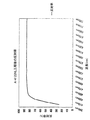
この問題を解決するために、460nmの青色域の波長を有する光を発光する青色LED103の代わりに430nm以下の青紫域の短波長を有する光を発光するLEDを用いることにより、蛍光体の励起効率を改善することが考えられる。しかしながら、発光波長が430nm以下の青紫から紫外領域になると、可視光領域のLEDデバイス100の枠体101として使用される前記高効率光反射樹脂(アモデル、ベクトラ材等)でも短波長域での光の反射率が急激に低下することにより、枠体101での反射(枠体101のすり鉢状の内壁面での反射)が得られず、LEDデバイス100の輝度低下の原因となる。図15に、枠体101に用いられるアモデルA−4122N材の反射率を示す。
【0008】
【発明が解決しようとする課題】
そこで、本発明では、色再現性がよく、高輝度な光源としてのLEDデバイスを提供することを課題とする。
【0009】
【課題を解決するための手段】
本発明は、前記課題を解決するための手段として、
上面開口のすり鉢状の凹部を有し、該凹部の内壁面を反射面とした枠体と、前記凹部の内底面に配置されたLEDチップと、該LEDチップからの発光の一部を吸収し、波長変換して発光する蛍光体を含み、前記凹部内に充填された樹脂とを備えるLEDデバイスにおいて、
前記反射面に前記蛍光体を含む蛍光体層を形成し、
前記蛍光体層は、前記LEDチップからの光により異なる波長の光を発光する複数の蛍光体層からなり、
前記複数の蛍光体層は、内側から外側に向かうほど短波長の光に励起変換する蛍光体層を配置したものである。
【0010】
前記発明によれば、LEDチップからの出射光が蛍光体層に到達すると、この蛍光体層に含まれる蛍光体がLEDチップからの光を波長変換して発光するので、出射光を効果的に励起変換することが可能となり、反射効率および輝度が向上する。
【0011】
前記LEDチップの発光波長は、430nm以下であることが好ましい。このように、青紫色領域の発光源を用いることにより、青色領域の波長の光では変換効率の低い赤、緑、青の3原色発光蛍光体を効率的に励起することが可能となる。
【0012】
前記蛍光体層は、励起発光波長の異なる複数の蛍光体層からなるが、本実施形態においては、前記蛍光体層は、3つの層からなり、それぞれの蛍光体層は、LEDチップからの光を赤、緑、青色の光に励起する。これにより、LEDデバイスの光度を飛躍的に向上し、赤、緑、青成分を含む演色性の高いLEDデバイスを提供できる。
【0013】
このとき、前記複数の蛍光体層は、内側から外側に向かうほど短波長の光に励起変換する蛍光体層が配置され、本実施形態においては、前記蛍光体層は、内側から外側に向かって順番にLEDチップからの光を赤、緑、青の光に励起するように配置されている。これにより、蛍光体への入射光が増加し、光度の向上が図れる。
【0014】
前記蛍光体層が、真空蒸着、印刷、インクジェット塗布法により形成されることが好ましい。
【0015】
前記蛍光体は、Siを主成分とするマイクロカプセルで覆われていることが好ましい。これにより、LEDチップからの出射光の透過を防止し、出射光を励起して反射する効率を向上できる。
【0016】
前記枠体は、ガラス材または金属材料からなることが好ましい。枠体をガラス材により構成すると、凹部の内壁面(反射面)に到達した光が内壁面を透過することを低減し、一方、枠体を金属材料から構成すると、凹部の内壁面(反射面)において光の波長毎による反射率の低減を改善できる。
【0017】
前記蛍光体層は、前記反射面に施された金属めっきの上に重ねて形成されることが好ましい。
【0018】
さらに、前記金属めっきは、前記金属めっきのめっき液に前記蛍光体を分散させながら電着させるコンポジットめっき法により施されることがより好ましい。
【0020】
前記凹部内に充填された樹脂の表層部には、表面積の10%以下の割合で分散する表面が鏡面である鏡面粒子が含まれているので、LEDチップから樹脂の表層部に到達した光が、この鏡面粒子で反射され再びデバイス内部に戻り、樹脂内部の蛍光体を励起することによりLEDチップからの光の波長変換効率が向上する。
【0021】
また、前記LEDデバイスは、前記樹脂と別体で、前記凹部の開口部に設けられたまたは貼着された表面が鏡面である鏡面粒子を含む反射樹脂層またはシート状の反射樹脂層を備えてもよい。これにより、LEDチップから反射樹脂層またはシート状の反射樹脂層に到達した光が、鏡面粒子で反射され再びデバイス内部に戻り、樹脂内部の蛍光体を励起することにより光の波長変換効率が向上する。
【0022】
前記樹脂に任意の色素を混合してもよい。これにより、長時間のLEDデバイスを使用するとLEDチップの劣化が生じた場合でも、色素の色抜けが起きることで樹脂の透過率が向上し、結果的に、見かけ上のLEDデバイスの輝度低下を防止することができる。
【0023】
前記LEDデバイスは、前記凹部の開口部に波長が400nm以下の紫外線をカットする紫外線カットフィルタもしくは紫外線反射材を備えることにより、紫外線によるユーザへの影響を軽減できる。
【0024】
前記LEDデバイスは、前記凹部の開口部に、前記蛍光体を含み、表面をレーザトリミング法によりトリミングした蛍光体薄層が設けられていることが好ましい。これにより、LEDデバイスにおいて所望の波長が得られ、LEDデバイスが発光する色調のバラツキを抑えることができる。
【0025】
前記枠体内部にヒートパイプを備えることが好ましい。
【0026】
前記枠体の下部中央部を下方に突出させることが好ましい。
【0027】
【発明の実施の形態】
以下、本発明の実施の形態を添付図面に従って説明する。
【0028】
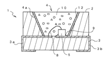
図1は、本発明に係るLEDデバイス1の斜視図であり、図2は、その断面図である。このLEDデバイス1は、矩形状の枠体2および電気的接続するための金属フレーム3を備えている。この枠体2は、例えば、アモデル材やベクトラ材などの可視光の反射効率の高い樹脂材料からなり、枠体2の中央部には、上面開口のすり鉢状の凹部4が形成されている。該凹部4の内底面かつ前記金属フレーム3上には、LEDチップ5(発光ダイオード)が配置されている。また、前記すり鉢状の凹部4の内壁面(反射面)4aは、前記LEDチップ5から放出された出射光を反射し、枠体2が出射光を吸収することを防止するようになっている。前記金属フレーム3は、前記枠体2をインサート成型する際に前記枠体2の内部に配置され、端子電極3a,3bを構成している。
【0029】
前記凹部4の内壁面4aには、蛍光体層6が形成されている。この蛍光体層6は、図3に示すように、異なる波長の光を励起する複数の蛍光体層6からなり、具体的には、内側から外側に向かって第1層6a、第2層6bおよび第3層6cの3層構造からなっている。前記第1層6a、第2層6bおよび第3層6cは、前記LEDチップ5の発光波長を赤、緑、青に励起変換する(LEDチップ5からの発光の一部を吸収し、波長変換して発光する)蛍光体7a,b,cをそれぞれ含む。前記蛍光体層6の形成方法として、第3層6c、第2層6b、第1層6aの順番で真空蒸着を行ったり、インクジェット塗布法により印刷塗布したり、第3層6c、第2層6b、第1層6aの順番に印刷埋め込みし、不要部分を除去すればよい。または、すり鉢状の凹部4の内壁面4aに嵌合するようにあらかじめ成型した蛍光体層6を、凹部4の内壁面4aに接着してもよい。本実施形態においては、各蛍光体7a,b,cをそれぞれ含む3種類の蛍光体層6a,b,cを設けたが、いずれか1つの蛍光体層6のみを設け、すり鉢状の凹部4の内壁面4aにおけるLEDチップ5の出射光の吸収を防止するようにしてもよい。
【0030】
前記LEDチップ5は、前記金属フレーム3の端子電極3aとAuワイヤ線8でボンディングされ、端子電極3bと導電性接着剤9を介して、電気的接続が達成されている。このLEDチップ5は、通電されると発光波長が430nm以下の青紫から紫外領域の光を出射するものである。
【0031】
また、前記凹部4内部かつ前記LEDチップ5の周囲には、透光性の樹脂10、例えば、エポキシ系樹脂、シリコン系樹脂、アクリル系樹脂などの樹脂が充填(封止)されており、LEDチップ5の固定および保護が図られている。この透光性樹脂10には、前記蛍光体7a,b,cが混練されている。
【0032】
次に、前記構成からなるLEDデバイス1の作用について説明する。
【0033】
端子電極3a,3b間に通電されてLEDチップ5が発光すると、LEDチップ5から出射された出射光は、透光性樹脂10内を通過し、LEDデバイス1の発光面すなわち凹部4の開口部から天面方向に出射される。また、LEDチップ5から出射された出射光の一部は、透光性樹脂10に混練された蛍光体7a,b,cによりLED出射光の波長より長波長側、具体的には、赤色波長、緑色波長、青色波長に波長変換され、透光性樹脂10内で所望の色度座標にミキシングされLEDデバイス1の発光面から出射される。このとき、LEDチップ5から出射された出射光の波長は430nm以下であるので、青色域の波長、例えば、460nmの波長を有する光により蛍光体7a,b,cを励起する場合に比べて励起効率が向上し、LEDデバイス1の発光面から出射される輝度および光度が向上する。また、色の3原色である赤、緑、青の混色が得られるので色品位のよい白色LEDが得られる。
【0034】
また、LEDチップ5から出射された出射光の一部は、透光性樹脂10内を通過し、内壁面4aに塗布された蛍光体層6に到達する。このとき、LEDチップ5からの出射光は、蛍光体層6の蛍光体7a,b,cによりLED出射光の波長より長波長側に波長変換される。具体的には、まず、LED出射光は、蛍光体層6の第1層6aに含まれる蛍光体7aで赤色波長側に波長変換される。第1層6aを透過した残りの出射光は、次に蛍光体層6の第2層6bに含まれる蛍光体7bで緑色波長側に波長変換される。さらに、第2層6bを透過した残りの出射光は、蛍光体層6の第3層6cに含まれる蛍光体7cで青色波長側に波長変換される。このように、出射光は、蛍光体層6の第1層6a、第2層6bおよび第3層6cに順次到達し、それぞれの場所で赤、緑、青色波長を有する光に励起される。このとき、蛍光体層6は、内側から外側に向かうほど短波長の光に励起されるように配置されているので、出射光を屈折率の違いにより効果的に励起変換することが可能となり、反射効率が向上できる。また、蛍光体層6の各層への入射光が増加し、輝度および光度の向上が図れる。
【0035】
そして、前記蛍光体層6で励起変換され、最終的に凹部4の反射面である内壁面4aに到達した(可視光域の)光は、枠体2を構成する樹脂の反射特性により効率良く反射され、透光性樹脂10内、もしくはデバイス1の発光面に到達することになる。これにより、内壁面4aを透過する光を大幅に低減できる。以上のようにして、最終的にデバイス1の発光面に到達する光量が向上し、光度および輝度が向上する。
【0036】
前記実施形態の変形例として、図4に示すように、3種類の蛍光体7a,b,cを含む蛍光体層6’を形成してもよい。この蛍光体層6’には、上下方向において蛍光体7a,b,cが順番に配置されている。このような蛍光体層6’でも前述した作用と同様に、出射光を効果的に励起することが可能となり、反射効率が向上できる。
【0037】
また、図5に示すように、透光性の樹脂10と一緒に封止する蛍光体7a,b,cをSiを主成分とするマイクロカプセル11で覆うことにより、LEDチップ5からの出射光の透過を防止し、反射の効率を向上させてもよい。
【0038】
また、前記実施形態の他の変形例として、枠体2を樹脂材料で構成するのでなく、ガラス材から構成してもよい。ガラス材は、最終的に凹部4の内壁面4aに到達した光が内壁面4aを透過することを低減する。また、枠体2を金属材料から構成してもよい。このとき、凹部4の内壁面4a(反射面)において光の波長毎による反射率の低減を改善できる。
【0039】
また、他の変形例として、凹部4の内壁面4a(反射面)にニッケルめっき、銅めっき等の金属めっきを施してもよい。この金属めっきにより、前述した場合と同様に、反射面において光の波長毎による反射率の低減を改善できる。このとき、反射面に金属めっきを施した後で前記蛍光体層6を重ねて設けることが好ましい。また、金属めっきのめっき液に蛍光体7a,b,cを分散させながら電着させるコンポジットめっき法により金属めっきを施してもよい。このように金属めっきすることにより、蛍光体励起による波長変換と金属面による反射効果を同時に得ることが可能となり、製造工程が簡略化する。
【0040】
また、図6に示すように、反射面に蛍光体層6を塗布する代わりに、凹部4の内壁面4aでの光の吸収を防止する酸化チタン等の紫外線反射材12を塗布してもよい。
【0041】
また、すり鉢状の凹部4内にモールドする透光性の樹脂10に、この樹脂10の比重より小さい比重を有し、かつ表面が鏡面である鏡面粒子13を透光性の樹脂10の1%以下の比率で混合してもよい。このとき、図7に示すように、樹脂10が硬化した後、鏡面粒子13は、LEDデバイス1の発光面すなわち凹部4内に充填された樹脂10の表層部に表面積の10%以下の割合で分散する。これにより、LEDチップ5から樹脂10の表層部に到達した光が、鏡面粒子13で反射され再びデバイス1内部に戻り、透光性の樹脂10内の蛍光体7a,b,cで励起変換される。その結果、蛍光体7a,b,cへの入射効率が高くなり、波長変換率が向上することによりLEDデバイス1の光度および発光効率が改善される。
【0042】
また、前記鏡面粒子13を透光性樹脂10に混合させたものを凹部4内にモールドするのではなく、図8に示すように、透光性樹脂10と鏡面粒子13を混合させた反射樹脂層14を凹部4の開口部に別体に設け、2重モールド構造を形成してもよい。または、シート状の反射樹脂層14をLEDデバイス1の発光面すなわち凹部4の表層部に貼着してもよい。
【0043】
更に、前記実施形態の変形例として、前記透光性の樹脂10に任意の色素を混合して、初期状態での見かけ上の輝度を抑制するようにしてもよい。このLEDデバイス1を長時間使用すると、LEDチップ5が劣化してLEDチップ5の出力が低下するが、同時に色素の色抜けが生じて透光性の樹脂10の透過率が向上する。その結果、長時間使用した場合でも見かけ上のLEDデバイス1の輝度低下を防止し、長寿命デバイスを提供することができる。
【0044】
また、図9に示すように、LEDデバイス1の発光面すなわち凹部4開口部に、波長が400nm以下の紫外線をカットする紫外線カットフィルタもしくは紫外線反射材15を設けることにより、LEDチップ5から出射される430nm以下の短波長の光すなわち紫外線波長域の光のユーザへの影響を軽減し、アイセイフティーを図ることができる。
【0045】
また、LEDデバイス1の発光面に、赤、緑、青の蛍光体7a,b,cのうち任意の蛍光体7a,b,cを含む蛍光体薄層(不図示)を設け、LEDデバイス1の発光波長をモニタし、所望の波長を得るように発光面に設けた前記蛍光体薄層の表面をレーザトリミング法によりトリミングしてもよい。このようにLEDデバイス1の発光波長を所望の波長に補正することにより、全てのLEDデバイス1に対し単一の色調を得ることができ、LEDデバイス1が発光する色調のバラツキを抑えることができる。
【0046】
前記実施形態の変形例では、枠体2を金属材料から構成したが、このとき、枠体2内部にヒートパイプ(不図示)を配置してもよい。これにより、LEDデバイス1の熱抵抗を低減でき、LEDチップ5を大電流で駆動することが可能となりLEDデバイス1の輝度が高くなる。
【0047】
さらに、図10に示すように、前記枠体2の下部中央部を下方に突出させ、この突出部分2aをLEDデバイス1を実装する実装基板16(Al基板等の放熱用基板)に嵌合させてもよい。これにより、LEDチップ5での発熱を枠体2の突出部分2aを介して実装基板16(外部)に放出することで、熱抵抗を下げ、LEDチップ駆動電流を上げることが可能で、結果的にLEDデバイス1の光度が明るくなる。なお、前記枠体2の突出部分2aは、金属フレーム3の低部17よりも低い位置に位置するように設計されている。
【0048】
なお、前記実施形態におけるLEDチップ5の端子電極3a,3bとの電気的接続方法は、これに限定されるものではない。例えば、図11に示すように、金属フレーム3の端子電極3a,3bとLEDチップ5をAuワイヤ線8a,bでボンディングすることにより電気的接続を達成してもよい。また、図12に示すように、フェイスダウン工法により端子電極3a,3bとLEDチップ5とをバンプ接続することにより電気的接続を達成してもよい。
【0049】
また、前記実施形態では、LEDチップ5の実装部を成型樹脂によるインサート成形品(枠体2)と金属フレーム3とで構成したものを用いたが、図13に示すように、金属フレーム3の代わりに、例えば、ガラスエポキシ材、セラミック材等で形成した基板18を設け、その上に枠体2を一体に成型してもよい。また、枠体2は、ガラスエポキシ材等からなる板を貼り合わせることにより形成してもよい。
【0050】
【発明の効果】
以上の説明から明らかなように、本発明は、上面開口のすり鉢状の凹部を有し、凹部の内壁面を反射面とした枠体と、凹部の内底面に配置されたLEDチップと、LEDチップからの発光の一部を吸収し、波長変換して発光する蛍光体を含み、凹部内に充填された樹脂とを備えるLEDデバイスにおいて、記反射面に前記蛍光体を含む蛍光体層を形成し、蛍光体層は、LEDチップからの光により異なる波長の光を発光する複数の蛍光体層からなるので、蛍光体層に含まれる蛍光体がLEDチップからの光を効果的に励起変換し、反射効率および輝度が向上するという効果を奏する。
【0051】
また、LEDチップの発光波長が430nm以下であっても、反射面での透過率が増加すること、および光反射効率が低下することを防止できるという効果をも奏する。
【図面の簡単な説明】
【図1】 本発明のLEDデバイスの斜視図である。
【図2】 図1のLEDデバイスの断面図である。
【図3】 図2のLEDデバイスの一部拡大図である。
【図4】 図1のLEDデバイスの変形例を示す一部拡大図である。
【図5】 図1のLEDデバイスの変形例を示す断面図である。
【図6】 図1のLEDデバイスの変形例を示す断面図である。
【図7】 図1のLEDデバイスの変形例を示す断面図である。
【図8】 図1のLEDデバイスの変形例を示す断面図である。
【図9】 図1のLEDデバイスの変形例を示す断面図である。
【図10】 図1のLEDデバイスの変形例を示す断面図である。
【図11】 図1のLEDデバイスの変形例を示す断面図である。
【図12】 図1のLEDデバイスの変形例を示す断面図である。
【図13】 図1のLEDデバイスの変形例を示す斜視図である。
【図14】 従来のLEDデバイスを示す断面図である。
【図15】 枠体に用いられるアモデルA−4122N材の反射率を示すグラフである。
【符号の説明】
1…LEDデバイス
2…枠体
4…凹部
4a…凹部の内壁面、反射面
5…LEDチップ
6a,b,c…蛍光体層
7a,b,c…蛍光体
10…透光性の樹脂[0001]
BACKGROUND OF THE INVENTION
The present invention relates to an LED device mainly used for a backlight of a liquid crystal display such as a portable information terminal and various indicators. In particular, it is equipped with a phosphor that excites light of a wavelength different from the emission wavelength by light emitted from the LED, and is used as an LED light source for white or intermediate color emission.
[0002]
[Prior art]
Prior art documents related to the present invention include the following.
[0003]
[Patent Document 1]
JP 2000-223750 A (FIG. 2)
[0004]
In recent years, white LED devices have been used as backlight light sources for color LCDs due to an increase in demand for mobile phone devices and the like. A
[0005]
This
[0006]
However, since this pseudo white color is not obtained by mixing the three primary colors of red, green, and blue, there is a disadvantage that the red color reproducibility is particularly poor. For this reason, a white LED device (not shown) with good color quality in which the
[0007]
In order to solve this problem, the excitation efficiency of the phosphor is obtained by using an LED that emits light having a short wavelength in the blue-violet region of 430 nm or less instead of the
[0008]
[Problems to be solved by the invention]
Therefore, an object of the present invention is to provide an LED device as a light source with high color reproducibility and high brightness.
[0009]
[Means for Solving the Problems]
As a means for solving the above problems, the present invention provides:
It has a mortar-shaped recess having an opening on the top surface, a frame body having the inner wall surface of the recess as a reflection surface, an LED chip disposed on the inner bottom surface of the recess, and part of the light emitted from the LED chip. In an LED device comprising a phosphor that emits light after wavelength conversion, and a resin filled in the recess,
Forming a phosphor layer containing the phosphor on the reflective surface;
The phosphor layer is Ri Do a plurality of phosphor layers that emit light of different wavelengths by light from the LED chip,
The plurality of phosphor layers are arranged with phosphor layers that excite and convert light having a shorter wavelength from the inside toward the outside .
[0010]
According to the invention, when the emitted light from the LED chip reaches the phosphor layer, the phosphor contained in the phosphor layer emits light by converting the wavelength of the light from the LED chip. Excitation conversion is possible, and reflection efficiency and luminance are improved.
[0011]
The emission wavelength of the LED chip is preferably 430 nm or less. As described above, by using a light emission source in the blue-violet region, it is possible to efficiently excite the three primary color light-emitting phosphors of red, green, and blue, which have low conversion efficiency with light having a wavelength in the blue region.
[0012]
The phosphor layer is composed of a plurality of phosphor layers having different excitation emission wavelengths, but in the present embodiment, the phosphor layer is composed of three layers, and each phosphor layer is light from an LED chip. Are excited by red, green and blue light. Thereby, the luminous intensity of the LED device can be dramatically improved, and an LED device having high color rendering properties including red, green, and blue components can be provided.
[0013]
At this time, the plurality of phosphor layers are arranged such that a phosphor layer that is excited and converted into light having a shorter wavelength as it goes from the inside toward the outside, and in this embodiment, the phosphor layer is from the inside toward the outside. In order, the light from the LED chip is arranged to excite red, green and blue light. Thereby, the incident light to the phosphor increases, and the luminous intensity can be improved.
[0014]
The phosphor layer is preferably formed by vacuum deposition, printing, or inkjet coating.
[0015]
The phosphor is preferably covered with microcapsules containing Si as a main component. Thereby, the transmission of the emitted light from the LED chip can be prevented, and the efficiency of exciting and reflecting the emitted light can be improved.
[0016]
The frame body is preferably made of a glass material or a metal material. If the frame is made of a glass material, light reaching the inner wall surface (reflective surface) of the recess is reduced from being transmitted through the inner wall surface. On the other hand, if the frame is made of a metal material, the inner wall surface (reflective surface) of the recess is formed. ), It is possible to improve the reduction in reflectance due to the wavelength of light.
[0017]
It is preferable that the phosphor layer is formed so as to overlap the metal plating applied to the reflection surface.
[0018]
Furthermore, the metal plating is more preferably performed by a composite plating method in which electrodeposition is performed while dispersing the phosphor in the plating solution of the metal plating.
[0020]
Since the surface layer portion of the resin filled in the concave portion contains mirror surface particles whose surface is a mirror surface dispersed at a ratio of 10% or less of the surface area, the light that has reached the surface layer portion of the resin from the LED chip The wavelength conversion efficiency of light from the LED chip is improved by being reflected by the mirror particles and returning to the inside of the device again to excite the phosphor inside the resin.
[0021]
In addition, the LED device includes a reflective resin layer or a sheet-like reflective resin layer that is separate from the resin and includes specular particles whose surface provided or adhered to the opening of the concave portion is a mirror surface. Also good. As a result, the light reaching the reflective resin layer or the sheet-like reflective resin layer from the LED chip is reflected by the mirror particles and returns to the inside of the device again, and the wavelength conversion efficiency of the light is improved by exciting the phosphor inside the resin. To do.
[0022]
Arbitrary pigment | dyes may be mixed with the said resin. As a result, even when the LED chip is deteriorated when the LED device is used for a long time, the loss of color of the dye is improved, so that the resin transmittance is improved. As a result, the apparent brightness of the LED device is lowered. Can be prevented.
[0023]
The LED device can reduce the influence of the ultraviolet rays on the user by providing an ultraviolet cut filter or an ultraviolet reflecting material that cuts ultraviolet rays having a wavelength of 400 nm or less at the opening of the concave portion.
[0024]
In the LED device, it is preferable that a thin phosphor layer including the phosphor and having a surface trimmed by a laser trimming method is provided in the opening of the concave portion. Thereby, a desired wavelength is obtained in the LED device, and variation in color tone emitted from the LED device can be suppressed.
[0025]
It is preferable that a heat pipe is provided inside the frame.
[0026]
It is preferable to project the lower center portion of the frame body downward.
[0027]
DETAILED DESCRIPTION OF THE INVENTION
Hereinafter, embodiments of the present invention will be described with reference to the accompanying drawings.
[0028]
FIG. 1 is a perspective view of an
[0029]
A
[0030]
The
[0031]
Further, the inside of the
[0032]
Next, the operation of the
[0033]
When the
[0034]
Further, part of the emitted light emitted from the
[0035]
Then, the light that is excited and converted by the
[0036]
As a modification of the embodiment, as shown in FIG. 4, a
[0037]
Further, as shown in FIG. 5, the phosphors 7a, b, and c sealed together with the
[0038]
As another modification of the embodiment, the
[0039]
As another modification, the inner wall surface 4a (reflective surface) of the
[0040]
Further, as shown in FIG. 6, instead of applying the
[0041]
Further, the light-transmitting
[0042]
In addition, instead of molding the
[0043]
Furthermore, as a modification of the above embodiment, an arbitrary pigment may be mixed in the
[0044]
Further, as shown in FIG. 9, the
[0045]
Further, a phosphor thin layer (not shown) including any of phosphors 7a, b, and c of red, green, and blue phosphors 7a, b, and c is provided on the light emitting surface of the
[0046]
In the modification of the embodiment, the
[0047]
Further, as shown in FIG. 10, the lower central portion of the
[0048]
In addition, the electrical connection method with the terminal electrodes 3a and 3b of the
[0049]
Moreover, in the said embodiment, what comprised the mounting part of
[0050]
【The invention's effect】
As is clear from the above description, the present invention has a mortar-shaped recess having an opening on the top surface, a frame having the inner wall surface of the recess as a reflecting surface, an LED chip disposed on the inner bottom surface of the recess, and an LED. In a LED device including a phosphor that absorbs a part of light emitted from a chip and emits light by wavelength conversion, and a resin filled in a recess, a phosphor layer including the phosphor is formed on a reflective surface The phosphor layer is composed of a plurality of phosphor layers that emit light of different wavelengths depending on the light from the LED chip, so that the phosphor contained in the phosphor layer effectively excites and converts the light from the LED chip. There is an effect that the reflection efficiency and the luminance are improved.
[0051]
Moreover, even if the light emission wavelength of an LED chip is 430 nm or less, the effect that the transmittance | permeability in a reflective surface increases and the light reflection efficiency falls can also be show | played.
[Brief description of the drawings]
FIG. 1 is a perspective view of an LED device of the present invention.
FIG. 2 is a cross-sectional view of the LED device of FIG.
FIG. 3 is a partially enlarged view of the LED device of FIG. 2;
FIG. 4 is a partially enlarged view showing a modification of the LED device of FIG.
FIG. 5 is a cross-sectional view showing a modification of the LED device of FIG.
FIG. 6 is a cross-sectional view showing a modification of the LED device of FIG.
7 is a cross-sectional view showing a modification of the LED device of FIG. 1. FIG.
FIG. 8 is a cross-sectional view illustrating a modification of the LED device of FIG.
FIG. 9 is a cross-sectional view showing a modified example of the LED device of FIG.
10 is a cross-sectional view showing a modification of the LED device of FIG. 1. FIG.
11 is a cross-sectional view showing a modification of the LED device of FIG. 1. FIG.
12 is a cross-sectional view showing a modification of the LED device of FIG. 1. FIG.
13 is a perspective view showing a modification of the LED device of FIG. 1. FIG.
FIG. 14 is a cross-sectional view showing a conventional LED device.
FIG. 15 is a graph showing the reflectance of Amodel A-4122N material used for the frame.
[Explanation of symbols]
DESCRIPTION OF
Claims (10)
前記反射面に前記蛍光体を含む蛍光体層を形成し、
前記蛍光体層は、前記LEDチップからの光により異なる波長の光を発光する複数の蛍光体層からなり、
前記複数の蛍光体層は、内側から外側に向かうほど短波長の光に励起変換する蛍光体層を配置したことを特徴とするLEDデバイス。It has a mortar-shaped recess having an opening on the top surface, a frame body having the inner wall surface of the recess as a reflection surface, an LED chip disposed on the inner bottom surface of the recess, and part of the light emitted from the LED chip. In an LED device comprising a phosphor that emits light after wavelength conversion, and a resin filled in the recess,
Forming a phosphor layer containing the phosphor on the reflective surface;
The phosphor layer is Ri Do a plurality of phosphor layers that emit light of different wavelengths by light from the LED chip,
The LED device, wherein the plurality of phosphor layers are arranged with phosphor layers that excite and convert light having a shorter wavelength from the inside toward the outside .
Priority Applications (3)
| Application Number | Priority Date | Filing Date | Title |
|---|---|---|---|
| JP2002293693A JP3910517B2 (en) | 2002-10-07 | 2002-10-07 | LED device |
| US10/667,669 US6982522B2 (en) | 2002-10-07 | 2003-09-23 | LED device including phosphor layers on the reflecting surface |
| CNB031434908A CN1237631C (en) | 2002-10-07 | 2003-09-30 | LED device |
Applications Claiming Priority (1)
| Application Number | Priority Date | Filing Date | Title |
|---|---|---|---|
| JP2002293693A JP3910517B2 (en) | 2002-10-07 | 2002-10-07 | LED device |
Publications (3)
| Publication Number | Publication Date |
|---|---|
| JP2004128393A JP2004128393A (en) | 2004-04-22 |
| JP2004128393A5 JP2004128393A5 (en) | 2006-11-02 |
| JP3910517B2 true JP3910517B2 (en) | 2007-04-25 |
Family
ID=32040727
Family Applications (1)
| Application Number | Title | Priority Date | Filing Date |
|---|---|---|---|
| JP2002293693A Expired - Fee Related JP3910517B2 (en) | 2002-10-07 | 2002-10-07 | LED device |
Country Status (3)
| Country | Link |
|---|---|
| US (1) | US6982522B2 (en) |
| JP (1) | JP3910517B2 (en) |
| CN (1) | CN1237631C (en) |
Families Citing this family (92)
| Publication number | Priority date | Publication date | Assignee | Title |
|---|---|---|---|---|
| CN100420047C (en) * | 2003-12-26 | 2008-09-17 | 三洋电机株式会社 | Package for light emitting element and process for fabricating same |
| JP4547569B2 (en) * | 2004-08-31 | 2010-09-22 | スタンレー電気株式会社 | Surface mount type LED |
| JP4880887B2 (en) * | 2004-09-02 | 2012-02-22 | 株式会社東芝 | Semiconductor light emitting device |
| DE102004045950A1 (en) | 2004-09-22 | 2006-03-30 | Osram Opto Semiconductors Gmbh | Housing for an optoelectronic component, optoelectronic component and method for producing an optoelectronic component |
| CN101023535B (en) * | 2004-09-22 | 2010-06-02 | 株式会社东芝 | Light emitting device, and back light and liquid crystal display employing it |
| JP2006114854A (en) * | 2004-10-18 | 2006-04-27 | Sharp Corp | Semiconductor light emitting device, and backlight device for liquid crystal display |
| US20060082297A1 (en) * | 2004-10-19 | 2006-04-20 | Eastman Kodak Company | Method of preparing a lens-less LED |
| WO2006067885A1 (en) * | 2004-12-24 | 2006-06-29 | Kyocera Corporation | Light-emitting device and illuminating device |
| JP4748411B2 (en) * | 2005-01-06 | 2011-08-17 | 株式会社フジクラ | Light emitting device, method for adjusting chromaticity of light emitting device, and lighting apparatus |
| EP1694047B1 (en) * | 2005-02-16 | 2020-03-18 | X-Rite Switzerland GmbH | Lighting system for a colour measuring device |
| JP2006261292A (en) * | 2005-03-16 | 2006-09-28 | Sumitomo Metal Electronics Devices Inc | Light emitting element storage package |
| JP5238123B2 (en) * | 2005-03-18 | 2013-07-17 | 京セラ株式会社 | Fiber light source, fiber light source device, and endoscope using the same |
| US20080296589A1 (en) * | 2005-03-24 | 2008-12-04 | Ingo Speier | Solid-State Lighting Device Package |
| CN100373646C (en) * | 2005-03-25 | 2008-03-05 | 李洲科技股份有限公司 | Multi-wavelength LED structure and making process thereof |
| JP2006278980A (en) * | 2005-03-30 | 2006-10-12 | Sanyo Electric Co Ltd | Semiconductor light-emitting device |
| JP4574417B2 (en) * | 2005-03-31 | 2010-11-04 | シャープ株式会社 | Light source module, backlight unit, liquid crystal display device |
| CA2614803C (en) * | 2005-04-05 | 2015-08-25 | Tir Technology Lp | Electronic device package with an integrated evaporator |
| US8215815B2 (en) * | 2005-06-07 | 2012-07-10 | Oree, Inc. | Illumination apparatus and methods of forming the same |
| US8272758B2 (en) | 2005-06-07 | 2012-09-25 | Oree, Inc. | Illumination apparatus and methods of forming the same |
| US8128272B2 (en) | 2005-06-07 | 2012-03-06 | Oree, Inc. | Illumination apparatus |
| JP5020480B2 (en) * | 2005-06-14 | 2012-09-05 | 電気化学工業株式会社 | Phosphor composition and use thereof |
| JP2007088261A (en) * | 2005-09-22 | 2007-04-05 | Sanyo Electric Co Ltd | Light emitting apparatus |
| JP5074201B2 (en) * | 2005-11-24 | 2012-11-14 | 洋一 松岡 | Electronic component mounting board |
| US8395725B2 (en) | 2006-01-19 | 2013-03-12 | Kabushiki Kaisha Toshiba | Light emitting module, backlight using the same, and liquid crystal display device |
| JP4838005B2 (en) * | 2006-02-20 | 2011-12-14 | 京セラ株式会社 | Light emitting device |
| WO2007122543A2 (en) * | 2006-04-26 | 2007-11-01 | Philips Intellectual Property & Standards Gmbh | Light delivery device with improved conversion element |
| US7906794B2 (en) | 2006-07-05 | 2011-03-15 | Koninklijke Philips Electronics N.V. | Light emitting device package with frame and optically transmissive element |
| JP4937845B2 (en) * | 2006-08-03 | 2012-05-23 | 日立マクセル株式会社 | Illumination device and display device |
| JP4846498B2 (en) * | 2006-09-22 | 2011-12-28 | 株式会社東芝 | Optical semiconductor device and method for manufacturing optical semiconductor device |
| BRPI0718086A2 (en) * | 2006-10-31 | 2013-11-05 | Tir Technology Lp | LIGHTING DEVICE PACKAGING |
| RU2451366C2 (en) * | 2006-12-05 | 2012-05-20 | Конинклейке Филипс Электроникс Н.В. | Illumination device, particularly with luminescent ceramic |
| JP2010512662A (en) | 2006-12-11 | 2010-04-22 | ザ リージェンツ オブ ザ ユニバーシティ オブ カリフォルニア | Transparent light emitting diode |
| JP2008205170A (en) * | 2007-02-20 | 2008-09-04 | Nec Lighting Ltd | Light-emitting semiconductor device |
| TWI326923B (en) * | 2007-03-07 | 2010-07-01 | Lite On Technology Corp | White light emitting diode |
| EP2158429A2 (en) * | 2007-05-29 | 2010-03-03 | Oree, Advanced Illumination Solutions INC. | Method and device for providing circumferential illumination |
| KR101337602B1 (en) | 2007-06-01 | 2013-12-06 | 서울반도체 주식회사 | Light emitting device |
| US20090008662A1 (en) * | 2007-07-05 | 2009-01-08 | Ian Ashdown | Lighting device package |
| CN101419962B (en) * | 2007-10-24 | 2011-11-02 | 张守仁 | LED, production method therefore and illuminator manufactured by the LED |
| US8946987B2 (en) * | 2007-11-07 | 2015-02-03 | Industrial Technology Research Institute | Light emitting device and fabricating method thereof |
| US7929816B2 (en) * | 2007-12-19 | 2011-04-19 | Oree, Inc. | Waveguide sheet containing in-coupling, propagation, and out-coupling regions |
| US20090159915A1 (en) * | 2007-12-19 | 2009-06-25 | Shaul Branchevsky | Led insert module and multi-layer lens |
| US8172447B2 (en) * | 2007-12-19 | 2012-05-08 | Oree, Inc. | Discrete lighting elements and planar assembly thereof |
| JP5193586B2 (en) * | 2007-12-25 | 2013-05-08 | 株式会社東芝 | Semiconductor light emitting device |
| EP2260341A2 (en) | 2008-03-05 | 2010-12-15 | Oree, Advanced Illumination Solutions INC. | Illumination apparatus and methods of forming the same |
| JP4617367B2 (en) * | 2008-03-13 | 2011-01-26 | シャープ株式会社 | Headlamp and vehicle infrared night vision apparatus using the same as a light source |
| TW200941758A (en) | 2008-03-25 | 2009-10-01 | Bright Led Electronics Corp | LED-based surface light-source device |
| CN101545615B (en) * | 2008-03-27 | 2011-05-25 | 佰鸿工业股份有限公司 | Light emitting diode surface light source device |
| US8297786B2 (en) | 2008-07-10 | 2012-10-30 | Oree, Inc. | Slim waveguide coupling apparatus and method |
| US8301002B2 (en) * | 2008-07-10 | 2012-10-30 | Oree, Inc. | Slim waveguide coupling apparatus and method |
| JP2010027974A (en) * | 2008-07-23 | 2010-02-04 | Sharp Corp | Method of manufacturing light-emitting device |
| US20100098377A1 (en) * | 2008-10-16 | 2010-04-22 | Noam Meir | Light confinement using diffusers |
| US20100127289A1 (en) * | 2008-11-26 | 2010-05-27 | Bridgelux, Inc. | Method and Apparatus for Providing LED Package with Controlled Color Temperature |
| JP4808244B2 (en) * | 2008-12-09 | 2011-11-02 | スタンレー電気株式会社 | Semiconductor light emitting device and manufacturing method thereof |
| US20100208470A1 (en) * | 2009-02-10 | 2010-08-19 | Yosi Shani | Overlapping illumination surfaces with reduced linear artifacts |
| JP5689223B2 (en) * | 2009-03-05 | 2015-03-25 | 日亜化学工業株式会社 | Light emitting device |
| US8624527B1 (en) | 2009-03-27 | 2014-01-07 | Oree, Inc. | Independently controllable illumination device |
| US8328406B2 (en) * | 2009-05-13 | 2012-12-11 | Oree, Inc. | Low-profile illumination device |
| US8727597B2 (en) | 2009-06-24 | 2014-05-20 | Oree, Inc. | Illumination apparatus with high conversion efficiency and methods of forming the same |
| US8933644B2 (en) | 2009-09-18 | 2015-01-13 | Soraa, Inc. | LED lamps with improved quality of light |
| US9293667B2 (en) | 2010-08-19 | 2016-03-22 | Soraa, Inc. | System and method for selected pump LEDs with multiple phosphors |
| US20110186887A1 (en) * | 2009-09-21 | 2011-08-04 | Soraa, Inc. | Reflection Mode Wavelength Conversion Material for Optical Devices Using Non-Polar or Semipolar Gallium Containing Materials |
| KR101112463B1 (en) | 2009-11-30 | 2012-02-22 | 마이크로 인스펙션 주식회사 | Method for manufacturing led chip |
| US20110215348A1 (en) * | 2010-02-03 | 2011-09-08 | Soraa, Inc. | Reflection Mode Package for Optical Devices Using Gallium and Nitrogen Containing Materials |
| US8740413B1 (en) | 2010-02-03 | 2014-06-03 | Soraa, Inc. | System and method for providing color light sources in proximity to predetermined wavelength conversion structures |
| US8905588B2 (en) | 2010-02-03 | 2014-12-09 | Sorra, Inc. | System and method for providing color light sources in proximity to predetermined wavelength conversion structures |
| US10147850B1 (en) | 2010-02-03 | 2018-12-04 | Soraa, Inc. | System and method for providing color light sources in proximity to predetermined wavelength conversion structures |
| JP5678629B2 (en) * | 2010-02-09 | 2015-03-04 | ソニー株式会社 | Method for manufacturing light emitting device |
| JP2013168326A (en) * | 2012-02-16 | 2013-08-29 | Toshiba Lighting & Technology Corp | Lighting apparatus |
| WO2011125885A1 (en) * | 2010-03-31 | 2011-10-13 | インテックス株式会社 | Light-source device |
| US8889443B2 (en) | 2010-07-22 | 2014-11-18 | Nichia Corporation | Method of forming light converting layer, method of manufacturing light converting member, and method of manufacturing light emitting device |
| JP2012064728A (en) * | 2010-09-15 | 2012-03-29 | Stanley Electric Co Ltd | Light source device |
| CN102479906A (en) * | 2010-11-24 | 2012-05-30 | 展晶科技(深圳)有限公司 | Light-emitting diode capsulation structure |
| US20120235188A1 (en) * | 2011-03-15 | 2012-09-20 | Avago Technologies Ecbu Ip (Singapore) Pte. Ltd. | Method and Apparatus for a Flat Top Light Source |
| US8492746B2 (en) * | 2011-09-12 | 2013-07-23 | SemiLEDs Optoelectronics Co., Ltd. | Light emitting diode (LED) dice having wavelength conversion layers |
| JP2013062393A (en) * | 2011-09-14 | 2013-04-04 | Sharp Corp | Light emitting device |
| US8591072B2 (en) | 2011-11-16 | 2013-11-26 | Oree, Inc. | Illumination apparatus confining light by total internal reflection and methods of forming the same |
| CN104054189B (en) * | 2011-11-17 | 2018-06-26 | 株式会社流明斯 | Light-emitting element package body and the back light unit for including the light-emitting element package body |
| CN103311399B (en) * | 2012-03-15 | 2015-10-07 | 展晶科技(深圳)有限公司 | LED light emission device |
| WO2013147195A1 (en) * | 2012-03-30 | 2013-10-03 | 三菱化学株式会社 | Semiconductor light-emitting device, and illumination device |
| US9857519B2 (en) | 2012-07-03 | 2018-01-02 | Oree Advanced Illumination Solutions Ltd. | Planar remote phosphor illumination apparatus |
| JP6025144B2 (en) * | 2013-03-27 | 2016-11-16 | シチズン時計株式会社 | Light emitting device |
| JP6191453B2 (en) * | 2013-12-27 | 2017-09-06 | 日亜化学工業株式会社 | Light emitting device |
| US10024936B2 (en) | 2014-12-09 | 2018-07-17 | Synaptive Medical (Barbados) Inc. | System and method for electromagnet coil construction |
| CN104820815B (en) * | 2015-04-08 | 2017-11-24 | 王飞鸿 | A kind of LED reads pen |
| CN104964181B (en) * | 2015-06-19 | 2017-06-16 | 深圳联品激光技术有限公司 | A kind of fluorescent lamp |
| JP6590579B2 (en) * | 2015-08-03 | 2019-10-16 | シチズン電子株式会社 | LED light emitting device |
| US9865779B2 (en) | 2015-09-30 | 2018-01-09 | Nichia Corporation | Methods of manufacturing the package and light-emitting device |
| KR101813866B1 (en) * | 2015-12-15 | 2018-01-02 | (주)종로의료기 | The test device for Body fluid analysis using natural light |
| KR101977261B1 (en) * | 2017-11-03 | 2019-05-13 | 엘지전자 주식회사 | Phosphor module |
| CN109841164A (en) * | 2017-11-29 | 2019-06-04 | 利亚德光电股份有限公司 | Small spacing LED display module and preparation method thereof |
| US11592166B2 (en) | 2020-05-12 | 2023-02-28 | Feit Electric Company, Inc. | Light emitting device having improved illumination and manufacturing flexibility |
| US11876042B2 (en) | 2020-08-03 | 2024-01-16 | Feit Electric Company, Inc. | Omnidirectional flexible light emitting device |
Family Cites Families (8)
| Publication number | Priority date | Publication date | Assignee | Title |
|---|---|---|---|---|
| US5593782A (en) * | 1992-07-13 | 1997-01-14 | Minnesota Mining And Manufacturing Company | Encapsulated electroluminescent phosphor and method for making same |
| US5813753A (en) * | 1997-05-27 | 1998-09-29 | Philips Electronics North America Corporation | UV/blue led-phosphor device with efficient conversion of UV/blues light to visible light |
| JP3282176B2 (en) | 1997-07-14 | 2002-05-13 | 日亜化学工業株式会社 | Method of forming light emitting diode |
| JP3617587B2 (en) | 1997-07-17 | 2005-02-09 | 日亜化学工業株式会社 | Light emitting diode and method for forming the same |
| JP3407608B2 (en) | 1997-07-28 | 2003-05-19 | 日亜化学工業株式会社 | Light emitting diode and method for forming the same |
| JP3367096B2 (en) | 1999-02-02 | 2003-01-14 | 日亜化学工業株式会社 | Method of forming light emitting diode |
| DE60137995D1 (en) * | 2000-08-09 | 2009-04-30 | Avago Technologies General Ip | Light-emitting devices |
| JP4172196B2 (en) * | 2002-04-05 | 2008-10-29 | 豊田合成株式会社 | Light emitting diode |
-
2002
- 2002-10-07 JP JP2002293693A patent/JP3910517B2/en not_active Expired - Fee Related
-
2003
- 2003-09-23 US US10/667,669 patent/US6982522B2/en not_active Expired - Lifetime
- 2003-09-30 CN CNB031434908A patent/CN1237631C/en not_active Expired - Fee Related
Also Published As
| Publication number | Publication date |
|---|---|
| US20040066140A1 (en) | 2004-04-08 |
| US6982522B2 (en) | 2006-01-03 |
| CN1497742A (en) | 2004-05-19 |
| JP2004128393A (en) | 2004-04-22 |
| CN1237631C (en) | 2006-01-18 |
Similar Documents
| Publication | Publication Date | Title |
|---|---|---|
| JP3910517B2 (en) | LED device | |
| JP4254266B2 (en) | LIGHT EMITTING DEVICE AND LIGHT EMITTING DEVICE MANUFACTURING METHOD | |
| JP3717480B2 (en) | Semiconductor light emitting device | |
| JP4172196B2 (en) | Light emitting diode | |
| JP4077170B2 (en) | Semiconductor light emitting device | |
| JP4122739B2 (en) | Light emitting device and manufacturing method thereof | |
| WO2011132716A1 (en) | Semiconductor light emitting device and production method for semiconductor light emitting device | |
| JP2003017751A (en) | Light emitting diode | |
| TW201013982A (en) | White light led, and backlight and liquid crystal display device using the same | |
| WO2010029872A1 (en) | Light emitting unit, light emitting module, and display device | |
| JP2003051622A (en) | White light emitting semiconductor device | |
| JP2011222641A (en) | Light-emitting device | |
| JP2010087324A (en) | Light emitting device | |
| JP4771800B2 (en) | Semiconductor light emitting device and manufacturing method thereof | |
| WO2011129429A1 (en) | Led light-emitting device | |
| JP2019029386A (en) | Light-emitting device and manufacturing method thereof | |
| JP5082427B2 (en) | Light emitting device | |
| JP4747704B2 (en) | Method for manufacturing light emitting device with phosphor layer | |
| JP2007173408A (en) | Light-emitting device | |
| JP2003243724A (en) | Light emitting apparatus | |
| JP2005332963A (en) | Light emitting device | |
| JP5786278B2 (en) | Light emitting device | |
| JP2004288760A (en) | Multilayered led | |
| JP5678462B2 (en) | Light emitting device | |
| JP2002064220A (en) | Light emitting diode lamp and phosphor used therein |
Legal Events
| Date | Code | Title | Description |
|---|---|---|---|
| A621 | Written request for application examination |
Free format text: JAPANESE INTERMEDIATE CODE: A621 Effective date: 20050525 |
|
| A521 | Request for written amendment filed |
Free format text: JAPANESE INTERMEDIATE CODE: A523 Effective date: 20060920 |
|
| A871 | Explanation of circumstances concerning accelerated examination |
Free format text: JAPANESE INTERMEDIATE CODE: A871 Effective date: 20060920 |
|
| A131 | Notification of reasons for refusal |
Free format text: JAPANESE INTERMEDIATE CODE: A131 Effective date: 20061024 |
|
| A975 | Report on accelerated examination |
Free format text: JAPANESE INTERMEDIATE CODE: A971005 Effective date: 20061213 |
|
| A521 | Request for written amendment filed |
Free format text: JAPANESE INTERMEDIATE CODE: A523 Effective date: 20061219 |
|
| TRDD | Decision of grant or rejection written | ||
| A01 | Written decision to grant a patent or to grant a registration (utility model) |
Free format text: JAPANESE INTERMEDIATE CODE: A01 Effective date: 20070116 |
|
| A61 | First payment of annual fees (during grant procedure) |
Free format text: JAPANESE INTERMEDIATE CODE: A61 Effective date: 20070124 |
|
| R150 | Certificate of patent or registration of utility model |
Ref document number: 3910517 Country of ref document: JP Free format text: JAPANESE INTERMEDIATE CODE: R150 Free format text: JAPANESE INTERMEDIATE CODE: R150 |
|
| FPAY | Renewal fee payment (event date is renewal date of database) |
Free format text: PAYMENT UNTIL: 20100202 Year of fee payment: 3 |
|
| FPAY | Renewal fee payment (event date is renewal date of database) |
Free format text: PAYMENT UNTIL: 20110202 Year of fee payment: 4 |
|
| FPAY | Renewal fee payment (event date is renewal date of database) |
Free format text: PAYMENT UNTIL: 20120202 Year of fee payment: 5 |
|
| FPAY | Renewal fee payment (event date is renewal date of database) |
Free format text: PAYMENT UNTIL: 20130202 Year of fee payment: 6 |
|
| FPAY | Renewal fee payment (event date is renewal date of database) |
Free format text: PAYMENT UNTIL: 20130202 Year of fee payment: 6 |
|
| FPAY | Renewal fee payment (event date is renewal date of database) |
Free format text: PAYMENT UNTIL: 20140202 Year of fee payment: 7 |
|
| LAPS | Cancellation because of no payment of annual fees |